WO2013172065A1 - 記憶回路 - Google Patents
記憶回路 Download PDFInfo
- Publication number
- WO2013172065A1 WO2013172065A1 PCT/JP2013/054051 JP2013054051W WO2013172065A1 WO 2013172065 A1 WO2013172065 A1 WO 2013172065A1 JP 2013054051 W JP2013054051 W JP 2013054051W WO 2013172065 A1 WO2013172065 A1 WO 2013172065A1
- Authority
- WO
- WIPO (PCT)
- Prior art keywords
- data
- circuit
- nonvolatile
- bistable circuit
- bistable
- Prior art date
Links
Images


Classifications
-
- G—PHYSICS
- G11—INFORMATION STORAGE
- G11C—STATIC STORES
- G11C11/00—Digital stores characterised by the use of particular electric or magnetic storage elements; Storage elements therefor
- G11C11/02—Digital stores characterised by the use of particular electric or magnetic storage elements; Storage elements therefor using magnetic elements
- G11C11/14—Digital stores characterised by the use of particular electric or magnetic storage elements; Storage elements therefor using magnetic elements using thin-film elements
- G11C11/15—Digital stores characterised by the use of particular electric or magnetic storage elements; Storage elements therefor using magnetic elements using thin-film elements using multiple magnetic layers
-
- G—PHYSICS
- G11—INFORMATION STORAGE
- G11C—STATIC STORES
- G11C11/00—Digital stores characterised by the use of particular electric or magnetic storage elements; Storage elements therefor
- G11C11/02—Digital stores characterised by the use of particular electric or magnetic storage elements; Storage elements therefor using magnetic elements
- G11C11/16—Digital stores characterised by the use of particular electric or magnetic storage elements; Storage elements therefor using magnetic elements using elements in which the storage effect is based on magnetic spin effect
- G11C11/165—Auxiliary circuits
- G11C11/1673—Reading or sensing circuits or methods
-
- G—PHYSICS
- G11—INFORMATION STORAGE
- G11C—STATIC STORES
- G11C11/00—Digital stores characterised by the use of particular electric or magnetic storage elements; Storage elements therefor
- G11C11/02—Digital stores characterised by the use of particular electric or magnetic storage elements; Storage elements therefor using magnetic elements
- G11C11/16—Digital stores characterised by the use of particular electric or magnetic storage elements; Storage elements therefor using magnetic elements using elements in which the storage effect is based on magnetic spin effect
- G11C11/165—Auxiliary circuits
- G11C11/1675—Writing or programming circuits or methods
-
- G—PHYSICS
- G11—INFORMATION STORAGE
- G11C—STATIC STORES
- G11C11/00—Digital stores characterised by the use of particular electric or magnetic storage elements; Storage elements therefor
- G11C11/02—Digital stores characterised by the use of particular electric or magnetic storage elements; Storage elements therefor using magnetic elements
- G11C11/16—Digital stores characterised by the use of particular electric or magnetic storage elements; Storage elements therefor using magnetic elements using elements in which the storage effect is based on magnetic spin effect
- G11C11/165—Auxiliary circuits
- G11C11/1677—Verifying circuits or methods
-
- G—PHYSICS
- G11—INFORMATION STORAGE
- G11C—STATIC STORES
- G11C11/00—Digital stores characterised by the use of particular electric or magnetic storage elements; Storage elements therefor
- G11C11/21—Digital stores characterised by the use of particular electric or magnetic storage elements; Storage elements therefor using electric elements
- G11C11/34—Digital stores characterised by the use of particular electric or magnetic storage elements; Storage elements therefor using electric elements using semiconductor devices
- G11C11/40—Digital stores characterised by the use of particular electric or magnetic storage elements; Storage elements therefor using electric elements using semiconductor devices using transistors
- G11C11/41—Digital stores characterised by the use of particular electric or magnetic storage elements; Storage elements therefor using electric elements using semiconductor devices using transistors forming static cells with positive feedback, i.e. cells not needing refreshing or charge regeneration, e.g. bistable multivibrator or Schmitt trigger
- G11C11/413—Auxiliary circuits, e.g. for addressing, decoding, driving, writing, sensing, timing or power reduction
-
- G—PHYSICS
- G11—INFORMATION STORAGE
- G11C—STATIC STORES
- G11C13/00—Digital stores characterised by the use of storage elements not covered by groups G11C11/00, G11C23/00, or G11C25/00
- G11C13/0002—Digital stores characterised by the use of storage elements not covered by groups G11C11/00, G11C23/00, or G11C25/00 using resistive RAM [RRAM] elements
- G11C13/0021—Auxiliary circuits
- G11C13/0069—Writing or programming circuits or methods
-
- G—PHYSICS
- G11—INFORMATION STORAGE
- G11C—STATIC STORES
- G11C14/00—Digital stores characterised by arrangements of cells having volatile and non-volatile storage properties for back-up when the power is down
- G11C14/0054—Digital stores characterised by arrangements of cells having volatile and non-volatile storage properties for back-up when the power is down in which the volatile element is a SRAM cell
- G11C14/0081—Digital stores characterised by arrangements of cells having volatile and non-volatile storage properties for back-up when the power is down in which the volatile element is a SRAM cell and the nonvolatile element is a magnetic RAM [MRAM] element or ferromagnetic cell
-
- G—PHYSICS
- G11—INFORMATION STORAGE
- G11C—STATIC STORES
- G11C13/00—Digital stores characterised by the use of storage elements not covered by groups G11C11/00, G11C23/00, or G11C25/00
- G11C13/0002—Digital stores characterised by the use of storage elements not covered by groups G11C11/00, G11C23/00, or G11C25/00 using resistive RAM [RRAM] elements
- G11C13/0021—Auxiliary circuits
- G11C13/0069—Writing or programming circuits or methods
- G11C2013/0076—Write operation performed depending on read result
-
- G—PHYSICS
- G11—INFORMATION STORAGE
- G11C—STATIC STORES
- G11C2207/00—Indexing scheme relating to arrangements for writing information into, or reading information out from, a digital store
- G11C2207/22—Control and timing of internal memory operations
- G11C2207/2263—Write conditionally, e.g. only if new data and old data differ
Definitions
- the power source of the bistable circuit can be shut off. Thereby, the power consumption at the time of standby can be significantly suppressed. However, during the period when the power is turned on, the power consumption is larger than that of a normal SRAM.
- the present invention has been made in view of the above problems, and aims to reduce power consumption.
- the nonvolatile element can store data of the bistable circuit by changing a resistance value.
- one end of the nonvolatile element is connected to a node in the bistable circuit, and the other end is connected to a control line, and the control unit is configured to control the control line when data is stored in the bistable circuit. Based on this voltage, it can be configured to determine whether or not the data of the bistable circuit and the nonvolatile element match.
- the bistable circuit includes a first node and a second node that are complementary, and the nonvolatile element has a first nonvolatile element having one end connected to the first node and the other end connected to the control line.
- An element and a second nonvolatile element having one end connected to the second node and the other end connected to the control line may be included.
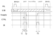
- FIG. 5A and FIG. 5B are block diagrams illustrating the memory circuit and the memory cell according to the first embodiment.
- the storage circuit 103 includes a memory area 77, a column decoder 71, a column driver 72, a row decoder 73, a row driver 74, and a control unit 85.
- a plurality of storage cells 100 are arranged in a matrix.
- Column decoder 71 and row decoder 73 select a column and a row from the address signal.
- the column driver 72 applies a voltage or the like to the input / output lines D and DB and the control line CTRL of the selected column.
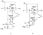
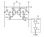
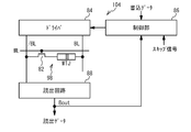
- the determination circuit 58 includes MOSFETs m10 to m15, sense amplifiers 65 and 66, inverters 63, 64 and 67, and an XOR circuit 68.
- MOSFETs m10 to m13 and inverter 63 electrically connect control line CTRL1 or CTRL2 connected to high-level node Q or QB to sense amplifier 65 via connection line CTRL (H) based on output Bout of buffer 62. To do.
- the control line CTRL1 or CTRL2 connected to the node Q or QB on the low level side is electrically connected to the sense amplifier 66 via the connection line CTRL (L).
- the sense amplifier 65 compares the voltage of the connection line CTRL (H) whose node is at a high level with the reference voltage VrefH.
- the output of the sense amplifier 65 is output as a match signal via the inverter 67.
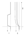
- connection line CTRL (L) When the corresponding ferromagnetic tunnel junction element has a high resistance (when the data does not match), the broken line appears.
- VrefL the reference voltage
- the control unit 85 determines that the data of the bistable circuit 30 and the ferromagnetic tunnel junction element are based on the output Bout of the readout circuit 56 and the voltage of the control line. It can be determined whether or not they match. For example, as shown in FIGS. 4A and 4B, one ferromagnetic tunnel junction element is provided between one node Q or QB in the bistable circuit 30 and the control line CTRL. Even in this case, it is possible to determine whether the data matches.
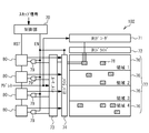
- FIG. 13 is a block diagram illustrating a memory circuit according to the fourth embodiment.
- the storage circuit 102 includes a memory area 77, a column decoder 71, a column driver 72, a row decoder 73, a row driver 74, a determination circuit 75, and a control unit 70.
- the memory area 77 a plurality of storage cells are arranged in a matrix.
- the memory cell is, for example, the memory cell shown in FIG. 2, FIG. 4 (a) or FIG. 4 (b).
- the memory area 77 is divided into a plurality of areas 76.
- Column decoder 71 and row decoder 73 select a column and a row from the address signal.
- the column driver 72 applies a voltage or the like to the input / output line and the control line of the selected column.
- the row driver 74 applies a voltage or the like to the word line, switch line, and control line of the selected row.
- the determination circuit 75 determines whether data has been volatilely rewritten in the memory cell in the corresponding region 76 during a predetermined period. For example, data is rewritten volatilely in the memory cell 78 of FIG.
- FIG. 14 is a flowchart showing processing of the control unit at the time of storing.
- the controller 70 volatilely rewrites data of a plurality of bistable circuits after the data is restored to the bistable circuit 30 last time for the first area 76. It is determined whether it has been (step S10). In the case of Yes, the control unit 70 stores the data of the bistable circuit 30 in a nonvolatile element (for example, a ferromagnetic tunnel junction element) in a nonvolatile manner in each memory cell in the region 76 (step S12). In the case of No, storing is not performed in the area 76. The control unit 70 determines whether it is the last region 76 (step S13). If yes, end. If No, the process returns to step S10.
- a nonvolatile element for example, a ferromagnetic tunnel junction element
- step S12 it may be determined whether the data of the bistable circuit 30 is stored in the nonvolatile element for each memory cell.
- the plurality of memory cells are divided into a plurality of regions 76, and the control unit 70 can determine whether to store the data of the bistable circuit 30 in the nonvolatile element for each of the plurality of regions. .
- FIG. 15 is a block diagram illustrating a memory circuit according to a modification of the fourth embodiment.
- AND circuit 79 and SRFF (SR flip-flop) 80 are provided corresponding to each region 76 in place of determination circuit 75 in FIG. 13.
- the AND circuit 79 performs an AND process between the rewrite activation signal EN and a signal indicating whether the memory cell to be volatilely rewritten is in the region 76. For example, it can be determined from the address signal whether the memory cell to be rewritten is within a specific area 76.
- the AND circuit 79 outputs a high level when the memory cell in the corresponding area 76 is to be rewritten, and outputs a low level when the memory cell in the corresponding area 76 is not to be rewritten.
- the storage unit stores, for each of the plurality of regions 76, whether or not at least one data of the bistable circuit 30 has been rewritten. Thereby, the control part 70 can determine easily whether at least 1 data of the bistable circuit 30 was rewritten.
- the ferromagnetic tunnel junction element has been described as an example of the nonvolatile element, but other nonvolatile elements may be used.
- the non-volatile element may be a resistance change element using a CER (Colossal Electro-Resistance) effect used for ReRAM (Resistance Random Access Memory) or the like. Further, it may be a phase change element or a ferroelectric element.
- FIG. 16 is a block diagram of a memory circuit in accordance with the fifth embodiment.
- the memory circuit 104 includes a MOSFET 82 and a ferromagnetic tunnel junction element MTJ as the memory cell 98.
- One of the source and drain of the MOSFET 82 is connected to the bit line / BL.
- the other of the source and drain of the MOSFET 82 is connected to the bit line BL via the ferromagnetic tunnel junction element MTJ.
- the gate of the MOSFET 82 is connected to the word line WL.
- a plurality of memory cells 98 are provided in a matrix.
- the driver 84 is connected to the bit lines / BL and BL.
- the driver 84 writes data to the storage cell 98 in a nonvolatile manner.
- the driver 84 sets one of the bit lines / BL and BL to the high level and the other to the low level.
- the word line WL is set to the high level to make the MOSFET 82 conductive.
- a current flows through the ferromagnetic tunnel junction device MTJ.
- the ferromagnetic tunnel junction element MTJ can have a low resistance or a high resistance, as described with reference to FIGS. Thereby, data can be written in the ferromagnetic tunnel junction device MTJ in a nonvolatile manner.
- the driver 84 does not write the write data to the memory cell 98 when the output of the XNOR circuit 92 is at a high level. For example, the driver 84 sets the bit lines / BL and BL to the same potential. Or let it float. As a result, no data is written to the ferromagnetic tunnel junction device MTJ even if the word line WL is at a high level. When the output of the XNOR circuit 92 is at a low level, write data is written into the memory cell 98.
- the voltage sense amplifier has been described, but a current sense amplifier can also be used.
- the memory circuit according to the first to fifth embodiments can be used for, for example, a cache memory, a register file, a register, or the like.
- a non-volatile memory such as a flash memory
- the writing operation to the cell may be repeated while checking (verifying) whether or not writing has been possible in order to prevent erroneous writing.
- the memory circuits of the first to fifth embodiments are different from such a verify operation, and confirm (match) the match between data that has already been normally written and the data to be overwritten.
- the verification for preventing erroneous writing is not used for a high-speed memory such as a cache memory because the verification is performed many times.
- the data match verification may be performed once for one write operation. Therefore, high-speed detection is possible, and it can be applied to a high-speed memory such as a cache memory.
Landscapes
- Engineering & Computer Science (AREA)
- Computer Hardware Design (AREA)
- Microelectronics & Electronic Packaging (AREA)
- Hall/Mr Elements (AREA)
- Mram Or Spin Memory Techniques (AREA)
- Static Random-Access Memory (AREA)
- Semiconductor Memories (AREA)
Abstract
Description
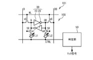
30 双安定回路
70、85、86 制御部
MTJ1、MTJ2 強磁性トンネル接合素子
Claims (17)
- データを記憶する双安定回路と、
前記双安定回路に記憶されたデータを不揮発的にストアし、不揮発的にストアされたデータを前記双安定回路にリストアする不揮発性素子と、
前記双安定回路と前記不揮発性素子とのデータが一致する場合は、前記双安定回路のデータを前記不揮発性素子にストアせず、前記双安定回路と前記不揮発性素子とのデータが一致しない場合は、前記双安定回路のデータを前記不揮発性素子にストアする制御部と、
を具備することを特徴とする記憶回路。 - 前記不揮発性素子は、抵抗値が変更されることにより前記双安定回路のデータをストアすることを特徴とする請求項1記載の記憶回路。
- 前記制御部は、前記双安定回路と前記不揮発性素子とのデータが一致するか否かを判定し、一致したと判定した場合、前記双安定回路のデータを前記不揮発性素子にストアせず、一致しないと判定した場合、前記双安定回路のデータを前記不揮発性素子にストアすることを特徴とする請求項1または2記載の記憶回路。
- 前記不揮発性素子は、一端が前記双安定回路内のノードに他端が制御線に接続され、
前記制御部は、前記双安定回路にデータが記憶されているときの前記制御線の電圧に基づき、前記双安定回路と前記不揮発性素子とのデータが一致するか否かを判定することを特徴とする請求項3記載の記憶回路。 - 前記双安定回路は、相補的な第1ノードおよび第2ノードを含み、
前記不揮発性素子は、一端が前記第1ノードに他端が前記制御線に接続された第1不揮発性素子と、一端が前記第2ノードに他端が前記制御線との間に接続された第2不揮発性素子と、を含むことを特徴とする請求項4記載の記憶回路。 - 前記双安定回路のデータを読み出す読出回路を具備し、
前記制御部は、前記読出回路の出力と、前記制御線の電圧と、に基づき、前記双安定回路と前記不揮発性素子とのデータが一致するか否かを判定することを特徴とする請求項4記載の記憶回路。 - 前記双安定回路は、相補的な第1ノードおよび第2ノードを含み、
前記制御線は、第1制御線と第2制御線とを含み、
前記不揮発性素子は、一端が前記第1ノードに他端が第1制御線に接続された第1不揮発性素子と、一端が前記第2ノードに他端が第2制御線との間に接続された第2不揮発性素子と、を含み、
前記制御部は、前記読出回路の出力と、前記第1制御線および前記第2制御線の電圧と、に基づき、前記第1不揮発性素子と前記第2不揮発性素子とのデータが矛盾するか否かを判定することを特徴とする請求項6記載の記憶回路。 - 前記制御部は、スキップ信号を受信した場合、前記双安定回路と前記不揮発性素子とのデータが一致するか否かの判定を行なわないことを特徴とする請求項3から7のいずれか一項記載の記憶回路。
- それぞれが、データを記憶する双安定回路と、前記双安定回路に記憶されたデータを不揮発的にストアし、不揮発的にストアされたデータを前記双安定回路にリストアする複数の不揮発性素子と、を有する複数のセルと、
前回に前記双安定回路にデータがリストアされた以降に、前記複数の双安定回路のデータが揮発的に書き換えられていない場合、前記複数のセルにおいて前記双安定回路のデータを前記不揮発性素子にストアせず、前記複数の双安定回路の少なくとも1つのデータが書き換えられた場合、前記複数のセルの少なくとも一部において前記双安定回路のデータを前記不揮発性素子にストアする制御部と、
を具備することを特徴とする記憶回路。 - 前記制御部は、前回に前記双安定回路にデータがリストアされた以降に、前記複数の双安定回路のデータが揮発的に書き換えられているか否かを判定し、書き換えられていないと判定した場合、前記複数のセルにおいて前記双安定回路のデータを前記不揮発性素子にストアせず、書き換えられたと判定した場合、前記複数のセルの少なくとも一部において前記双安定回路のデータを前記不揮発性素子にストアすることを特徴とする請求項9記載の記憶回路。
- 前記複数のセルは複数の領域に分割されており、
前記制御部は、前記複数の領域毎に、前記双安定回路のデータを前記不揮発性素子にストアするか否かを判断することを特徴とする請求項9または10記載の記憶回路。 - 前記複数の領域毎に、前記双安定回路の少なくとも1つのデータが書き換えられたか否かを記憶する記憶部を具備することを特徴とする請求項11記載の記憶回路。
- 前記制御部は、スキップ信号を受信した場合、前回に前記双安定回路にデータがリストアされた以降に、前記複数の双安定回路のデータが揮発的に書き換えられているか否かの判定を行なわないことを特徴とする請求項10記載の記憶回路。
- 前記不揮発性素子は強磁性トンネル接合素子であることを特徴とする請求項1から13のいずれか一項記載の記憶回路。
- 強磁性トンネル接合素子と、
前記強磁性トンネル接合素子に不揮発的に書き込まれたデータを読み出す読出回路と、
前記読出回路の出力と、前記強磁性トンネル接合素子に不揮発的に書き込むデータと、が一致した場合、前記強磁性トンネル接合素子に前記不揮発的に書き込むデータを書き込まず、
前記読出回路の出力と、前記不揮発的に書き込むデータと、が一致しない場合、前記強磁性トンネル接合素子に前記不揮発的に書き込むデータを書き込む制御部と、
を具備することを特徴とする記憶回路。 - 前記制御部は、前記読出回路の出力と、前記強磁性トンネル接合素子に不揮発的に書き込むデータと、が一致するか否かを判定し、一致したと判定した場合、前記強磁性トンネル接合素子に前記不揮発的に書き込むデータを書き込まず、一致しないと判定した場合、前記強磁性トンネル接合素子に前記不揮発的に書き込むデータを書き込むことを特徴とする請求項15記載の記憶回路。
- 前記制御部は、スキップ信号を受信した場合、前記読出回路の出力と、前記強磁性トンネル接合素子に不揮発的に書き込むデータと、が一致しているか否かの判定を行なわないことを特徴とする請求項16記載の記憶回路。
Priority Applications (7)
| Application Number | Priority Date | Filing Date | Title |
|---|---|---|---|
| EP16181451.2A EP3107105B1 (en) | 2012-05-18 | 2013-02-19 | Memory circuit |
| KR1020147032134A KR101666537B1 (ko) | 2012-05-18 | 2013-02-19 | 기억 회로 |
| CN201380025692.9A CN104303234B (zh) | 2012-05-18 | 2013-02-19 | 存储电路 |
| JP2013540169A JP5479656B1 (ja) | 2012-05-18 | 2013-02-19 | 記憶回路 |
| EP16180034.7A EP3109863B1 (en) | 2012-05-18 | 2013-02-19 | Memory circuit |
| EP13791432.1A EP2840575B1 (en) | 2012-05-18 | 2013-02-19 | Memory circuit |
| US14/546,668 US9496037B2 (en) | 2012-05-18 | 2014-11-18 | Memory circuit |
Applications Claiming Priority (2)
| Application Number | Priority Date | Filing Date | Title |
|---|---|---|---|
| JP2012-114988 | 2012-05-18 | ||
| JP2012114988 | 2012-05-18 |
Related Child Applications (1)
| Application Number | Title | Priority Date | Filing Date |
|---|---|---|---|
| US14/546,668 Continuation US9496037B2 (en) | 2012-05-18 | 2014-11-18 | Memory circuit |
Publications (1)
| Publication Number | Publication Date |
|---|---|
| WO2013172065A1 true WO2013172065A1 (ja) | 2013-11-21 |
Family
ID=49583490
Family Applications (1)
| Application Number | Title | Priority Date | Filing Date |
|---|---|---|---|
| PCT/JP2013/054051 WO2013172065A1 (ja) | 2012-05-18 | 2013-02-19 | 記憶回路 |
Country Status (7)
| Country | Link |
|---|---|
| US (1) | US9496037B2 (ja) |
| EP (3) | EP3107105B1 (ja) |
| JP (1) | JP5479656B1 (ja) |
| KR (1) | KR101666537B1 (ja) |
| CN (1) | CN104303234B (ja) |
| TW (1) | TWI582764B (ja) |
| WO (1) | WO2013172065A1 (ja) |
Cited By (6)
| Publication number | Priority date | Publication date | Assignee | Title |
|---|---|---|---|---|
| JP2016018573A (ja) * | 2014-07-07 | 2016-02-01 | 株式会社ソシオネクスト | データ保持回路および保持データ復元方法 |
| WO2016024527A1 (ja) * | 2014-08-12 | 2016-02-18 | 国立研究開発法人科学技術振興機構 | 記憶回路 |
| WO2016208407A1 (ja) * | 2015-06-24 | 2016-12-29 | ソニー株式会社 | 半導体装置 |
| WO2017150028A1 (ja) * | 2016-02-29 | 2017-09-08 | ソニー株式会社 | 半導体回路、半導体回路の駆動方法、および電子機器 |
| JP2018101456A (ja) * | 2016-12-16 | 2018-06-28 | 学校法人 芝浦工業大学 | 半導体装置 |
| WO2020241000A1 (ja) | 2019-05-30 | 2020-12-03 | 国立研究開発法人科学技術振興機構 | 電子回路および双安定回路 |
Families Citing this family (3)
| Publication number | Priority date | Publication date | Assignee | Title |
|---|---|---|---|---|
| US9805795B2 (en) * | 2016-01-08 | 2017-10-31 | Samsung Electronics Co., Ltd. | Zero leakage, high noise margin coupled giant spin hall based retention latch |
| US10476456B2 (en) | 2016-10-04 | 2019-11-12 | Mediatek Inc. | Comparator having a high-speed amplifier and a low-noise amplifier |
| JP6734904B2 (ja) * | 2018-11-01 | 2020-08-05 | ウィンボンド エレクトロニクス コーポレーション | 記憶回路 |
Citations (4)
| Publication number | Priority date | Publication date | Assignee | Title |
|---|---|---|---|---|
| JPH0281398A (ja) * | 1988-09-19 | 1990-03-22 | Hitachi Ltd | 半導体記憶装置 |
| JP2004063004A (ja) * | 2002-07-29 | 2004-02-26 | Sony Corp | 複合記憶回路構造及び同複合記憶回路構造を有する半導体装置 |
| WO2009028298A1 (ja) | 2007-08-31 | 2009-03-05 | Tokyo Institute Of Technology | スピン注入磁化反転mtjを用いた不揮発性sram/ラッチ回路 |
| US20100202191A1 (en) * | 2009-02-12 | 2010-08-12 | Seagate Technology Llc | nvSRAM HAVING VARIABLE MAGNETIC RESISTORS |
Family Cites Families (13)
| Publication number | Priority date | Publication date | Assignee | Title |
|---|---|---|---|---|
| JPH01154398A (ja) * | 1987-12-10 | 1989-06-16 | Fujitsu Ltd | 半導体記憶装置 |
| TW548653B (en) | 1999-01-26 | 2003-08-21 | Nec Electronics Corp | Semiconductor memory device having redundancy memory circuit |
| JP3701886B2 (ja) * | 2001-04-27 | 2005-10-05 | インターナショナル・ビジネス・マシーンズ・コーポレーション | 記憶回路ブロック及びアクセス方法 |
| JP4802415B2 (ja) | 2001-08-13 | 2011-10-26 | 日本テキサス・インスツルメンツ株式会社 | 強誘電体メモリ |
| JP4052829B2 (ja) * | 2001-12-12 | 2008-02-27 | 株式会社ルネサステクノロジ | 薄膜磁性体記憶装置 |
| US7869275B2 (en) * | 2006-10-07 | 2011-01-11 | Active-Semi, Inc. | Memory structure capable of bit-wise write or overwrite |
| JP2010033620A (ja) * | 2006-10-30 | 2010-02-12 | Renesas Technology Corp | 磁性体メモリ |
| JP4344011B2 (ja) * | 2007-08-01 | 2009-10-14 | パナソニック株式会社 | 不揮発性記憶装置 |
| JP5191834B2 (ja) * | 2008-08-12 | 2013-05-08 | セイコーインスツル株式会社 | 半導体不揮発性記憶装置 |
| JP5234547B2 (ja) | 2009-03-27 | 2013-07-10 | 国立大学法人東京工業大学 | 電子回路 |
| KR20110074285A (ko) * | 2009-12-24 | 2011-06-30 | 삼성전자주식회사 | 부분 셀프 리프레쉬를 수행하는 반도체 메모리 장치 및 이를 구비하는 반도체 메모리 시스템 |
| US8488363B2 (en) * | 2010-05-11 | 2013-07-16 | Qualcomm Incorporated | Write energy conservation in memory |
| JP2012133829A (ja) * | 2010-12-20 | 2012-07-12 | Sony Corp | 記憶装置、書込制御方法 |
-
2013
- 2013-02-19 WO PCT/JP2013/054051 patent/WO2013172065A1/ja active Application Filing
- 2013-02-19 CN CN201380025692.9A patent/CN104303234B/zh active Active
- 2013-02-19 JP JP2013540169A patent/JP5479656B1/ja active Active
- 2013-02-19 EP EP16181451.2A patent/EP3107105B1/en active Active
- 2013-02-19 EP EP16180034.7A patent/EP3109863B1/en active Active
- 2013-02-19 EP EP13791432.1A patent/EP2840575B1/en active Active
- 2013-02-19 KR KR1020147032134A patent/KR101666537B1/ko active IP Right Grant
- 2013-05-16 TW TW102117351A patent/TWI582764B/zh active
-
2014
- 2014-11-18 US US14/546,668 patent/US9496037B2/en active Active
Patent Citations (4)
| Publication number | Priority date | Publication date | Assignee | Title |
|---|---|---|---|---|
| JPH0281398A (ja) * | 1988-09-19 | 1990-03-22 | Hitachi Ltd | 半導体記憶装置 |
| JP2004063004A (ja) * | 2002-07-29 | 2004-02-26 | Sony Corp | 複合記憶回路構造及び同複合記憶回路構造を有する半導体装置 |
| WO2009028298A1 (ja) | 2007-08-31 | 2009-03-05 | Tokyo Institute Of Technology | スピン注入磁化反転mtjを用いた不揮発性sram/ラッチ回路 |
| US20100202191A1 (en) * | 2009-02-12 | 2010-08-12 | Seagate Technology Llc | nvSRAM HAVING VARIABLE MAGNETIC RESISTORS |
Non-Patent Citations (2)
| Title |
|---|
| See also references of EP2840575A4 |
| YUSUKE SHUTO ET AL.: "Evaluation and Control of Break-Even Time of Nonvolatile Static Random Access Memory Based on Spin-Transistor Architecture with Spin-Transfer-Torque Magnetic Tunnel Junctions", JAPANESE JOURNAL OF APPLIED PHYSICS, vol. 51, 30 March 2012 (2012-03-30), pages 040212, XP055167553 * |
Cited By (13)
| Publication number | Priority date | Publication date | Assignee | Title |
|---|---|---|---|---|
| JP2016018573A (ja) * | 2014-07-07 | 2016-02-01 | 株式会社ソシオネクスト | データ保持回路および保持データ復元方法 |
| WO2016024527A1 (ja) * | 2014-08-12 | 2016-02-18 | 国立研究開発法人科学技術振興機構 | 記憶回路 |
| KR20170023131A (ko) | 2014-08-12 | 2017-03-02 | 고쿠리츠켄큐카이하츠호진 카가쿠기쥬츠신코키코 | 기억 회로 |
| JPWO2016024527A1 (ja) * | 2014-08-12 | 2017-08-31 | 国立研究開発法人科学技術振興機構 | 記憶回路 |
| EP3828889A1 (en) | 2014-08-12 | 2021-06-02 | Japan Science and Technology Agency | Memory circuit |
| US10049740B2 (en) | 2014-08-12 | 2018-08-14 | Japan Science And Technology Agency | Memory circuit with a bistable circuit and a non-volatile element |
| US10373677B2 (en) | 2015-06-24 | 2019-08-06 | Sony Corporation | Semiconductor device to reduce energy consumed to write data |
| WO2016208407A1 (ja) * | 2015-06-24 | 2016-12-29 | ソニー株式会社 | 半導体装置 |
| US10460805B2 (en) | 2016-02-29 | 2019-10-29 | Sony Corporation | Semiconductor circuit, method of driving semiconductor circuit, and electronic apparatus |
| WO2017150028A1 (ja) * | 2016-02-29 | 2017-09-08 | ソニー株式会社 | 半導体回路、半導体回路の駆動方法、および電子機器 |
| JP2018101456A (ja) * | 2016-12-16 | 2018-06-28 | 学校法人 芝浦工業大学 | 半導体装置 |
| JP7007173B2 (ja) | 2016-12-16 | 2022-01-24 | ソニーセミコンダクタソリューションズ株式会社 | 半導体装置 |
| WO2020241000A1 (ja) | 2019-05-30 | 2020-12-03 | 国立研究開発法人科学技術振興機構 | 電子回路および双安定回路 |
Also Published As
| Publication number | Publication date |
|---|---|
| TW201411618A (zh) | 2014-03-16 |
| JP5479656B1 (ja) | 2014-04-23 |
| EP3109863A1 (en) | 2016-12-28 |
| EP3107105B1 (en) | 2021-06-16 |
| US9496037B2 (en) | 2016-11-15 |
| EP2840575B1 (en) | 2016-09-28 |
| CN104303234B (zh) | 2017-12-12 |
| US20150070975A1 (en) | 2015-03-12 |
| KR101666537B1 (ko) | 2016-10-14 |
| KR20150002835A (ko) | 2015-01-07 |
| TWI582764B (zh) | 2017-05-11 |
| CN104303234A (zh) | 2015-01-21 |
| EP2840575A1 (en) | 2015-02-25 |
| JPWO2013172065A1 (ja) | 2016-01-12 |
| EP3109863B1 (en) | 2023-07-26 |
| EP3107105A1 (en) | 2016-12-21 |
| EP2840575A4 (en) | 2015-07-08 |
Similar Documents
| Publication | Publication Date | Title |
|---|---|---|
| JP5479656B1 (ja) | 記憶回路 | |
| US20150036415A1 (en) | Non-volatile memory cell | |
| US8315090B2 (en) | Pseudo page mode memory architecture and method | |
| JP6230204B2 (ja) | 記憶回路 | |
| US20160078916A1 (en) | Fast programming of magnetic random access memory (mram) | |
| TWI508063B (zh) | Memory circuits with bistable circuits and nonvolatile components | |
| US20160276029A1 (en) | Non-volatile memory using bi-directional resistive elements | |
| JP2004103174A (ja) | 半導体記憶装置 | |
| US9824736B1 (en) | Memory device | |
| US10741233B2 (en) | Semiconductor memory device | |
| US9368208B1 (en) | Non-volatile latch using magneto-electric and ferro-electric tunnel junctions | |
| JP2003346473A (ja) | 薄膜磁性体記憶装置 | |
| CN110782923A (zh) | 存储器设备和驱动写入电流的方法 | |
| US9443585B2 (en) | Resistance change memory | |
| JP2016167333A (ja) | 疑似ページモードのメモリアーキテクチャおよび方法 | |
| US20230147686A1 (en) | Nonvolatile sram | |
| US11501811B2 (en) | Semiconductor storage device and controlling method thereof | |
| JP5312715B1 (ja) | 双安定回路と不揮発性素子とを備える記憶回路 | |
| JP5712681B2 (ja) | 半導体記憶装置 |
Legal Events
| Date | Code | Title | Description |
|---|---|---|---|
| ENP | Entry into the national phase |
Ref document number: 2013540169 Country of ref document: JP Kind code of ref document: A |
|
| 121 | Ep: the epo has been informed by wipo that ep was designated in this application |
Ref document number: 13791432 Country of ref document: EP Kind code of ref document: A1 |
|
| ENP | Entry into the national phase |
Ref document number: 20147032134 Country of ref document: KR Kind code of ref document: A |
|
| NENP | Non-entry into the national phase |
Ref country code: DE |
|
| REEP | Request for entry into the european phase |
Ref document number: 2013791432 Country of ref document: EP |
|
| WWE | Wipo information: entry into national phase |
Ref document number: 2013791432 Country of ref document: EP |