EP3107105B1 - Memory circuit - Google Patents
Memory circuit Download PDFInfo
- Publication number
- EP3107105B1 EP3107105B1 EP16181451.2A EP16181451A EP3107105B1 EP 3107105 B1 EP3107105 B1 EP 3107105B1 EP 16181451 A EP16181451 A EP 16181451A EP 3107105 B1 EP3107105 B1 EP 3107105B1
- Authority
- EP
- European Patent Office
- Prior art keywords
- data
- mtj2
- mtj1
- circuit
- nonvolatile element
- Prior art date
- Legal status (The legal status is an assumption and is not a legal conclusion. Google has not performed a legal analysis and makes no representation as to the accuracy of the status listed.)
- Active
Links
- 230000015654 memory Effects 0.000 title claims description 113
- 230000005294 ferromagnetic effect Effects 0.000 claims description 124
- 102100035420 DnaJ homolog subfamily C member 1 Human genes 0.000 claims description 48
- 101000804122 Homo sapiens DnaJ homolog subfamily C member 1 Proteins 0.000 claims description 48
- 230000000295 complement effect Effects 0.000 claims description 4
- 239000011159 matrix material Substances 0.000 claims description 4
- 210000004027 cell Anatomy 0.000 description 58
- 238000010586 diagram Methods 0.000 description 26
- 230000005415 magnetization Effects 0.000 description 23
- 238000000034 method Methods 0.000 description 11
- 230000004048 modification Effects 0.000 description 6
- 238000012986 modification Methods 0.000 description 6
- 238000012545 processing Methods 0.000 description 6
- 238000002347 injection Methods 0.000 description 5
- 239000007924 injection Substances 0.000 description 5
- 230000005291 magnetic effect Effects 0.000 description 4
- 230000008569 process Effects 0.000 description 4
- 239000004065 semiconductor Substances 0.000 description 4
- 230000009467 reduction Effects 0.000 description 3
- 239000002131 composite material Substances 0.000 description 2
- 230000008094 contradictory effect Effects 0.000 description 2
- 230000000694 effects Effects 0.000 description 2
- 229910044991 metal oxide Inorganic materials 0.000 description 2
- 150000004706 metal oxides Chemical class 0.000 description 2
- 238000013459 approach Methods 0.000 description 1
- 230000008859 change Effects 0.000 description 1
- 230000001419 dependent effect Effects 0.000 description 1
- 238000001514 detection method Methods 0.000 description 1
- 230000005669 field effect Effects 0.000 description 1
- 230000006870 function Effects 0.000 description 1
- 239000012212 insulator Substances 0.000 description 1
- 230000010354 integration Effects 0.000 description 1
- 239000002184 metal Substances 0.000 description 1
- 230000003068 static effect Effects 0.000 description 1
- 210000000352 storage cell Anatomy 0.000 description 1
- 238000012795 verification Methods 0.000 description 1
Images


Classifications
-
- G—PHYSICS
- G11—INFORMATION STORAGE
- G11C—STATIC STORES
- G11C11/00—Digital stores characterised by the use of particular electric or magnetic storage elements; Storage elements therefor
- G11C11/02—Digital stores characterised by the use of particular electric or magnetic storage elements; Storage elements therefor using magnetic elements
- G11C11/14—Digital stores characterised by the use of particular electric or magnetic storage elements; Storage elements therefor using magnetic elements using thin-film elements
- G11C11/15—Digital stores characterised by the use of particular electric or magnetic storage elements; Storage elements therefor using magnetic elements using thin-film elements using multiple magnetic layers
-
- G—PHYSICS
- G11—INFORMATION STORAGE
- G11C—STATIC STORES
- G11C14/00—Digital stores characterised by arrangements of cells having volatile and non-volatile storage properties for back-up when the power is down
- G11C14/0054—Digital stores characterised by arrangements of cells having volatile and non-volatile storage properties for back-up when the power is down in which the volatile element is a SRAM cell
- G11C14/0081—Digital stores characterised by arrangements of cells having volatile and non-volatile storage properties for back-up when the power is down in which the volatile element is a SRAM cell and the nonvolatile element is a magnetic RAM [MRAM] element or ferromagnetic cell
-
- G—PHYSICS
- G11—INFORMATION STORAGE
- G11C—STATIC STORES
- G11C11/00—Digital stores characterised by the use of particular electric or magnetic storage elements; Storage elements therefor
- G11C11/02—Digital stores characterised by the use of particular electric or magnetic storage elements; Storage elements therefor using magnetic elements
- G11C11/16—Digital stores characterised by the use of particular electric or magnetic storage elements; Storage elements therefor using magnetic elements using elements in which the storage effect is based on magnetic spin effect
- G11C11/165—Auxiliary circuits
- G11C11/1673—Reading or sensing circuits or methods
-
- G—PHYSICS
- G11—INFORMATION STORAGE
- G11C—STATIC STORES
- G11C11/00—Digital stores characterised by the use of particular electric or magnetic storage elements; Storage elements therefor
- G11C11/02—Digital stores characterised by the use of particular electric or magnetic storage elements; Storage elements therefor using magnetic elements
- G11C11/16—Digital stores characterised by the use of particular electric or magnetic storage elements; Storage elements therefor using magnetic elements using elements in which the storage effect is based on magnetic spin effect
- G11C11/165—Auxiliary circuits
- G11C11/1675—Writing or programming circuits or methods
-
- G—PHYSICS
- G11—INFORMATION STORAGE
- G11C—STATIC STORES
- G11C11/00—Digital stores characterised by the use of particular electric or magnetic storage elements; Storage elements therefor
- G11C11/02—Digital stores characterised by the use of particular electric or magnetic storage elements; Storage elements therefor using magnetic elements
- G11C11/16—Digital stores characterised by the use of particular electric or magnetic storage elements; Storage elements therefor using magnetic elements using elements in which the storage effect is based on magnetic spin effect
- G11C11/165—Auxiliary circuits
- G11C11/1677—Verifying circuits or methods
-
- G—PHYSICS
- G11—INFORMATION STORAGE
- G11C—STATIC STORES
- G11C11/00—Digital stores characterised by the use of particular electric or magnetic storage elements; Storage elements therefor
- G11C11/21—Digital stores characterised by the use of particular electric or magnetic storage elements; Storage elements therefor using electric elements
- G11C11/34—Digital stores characterised by the use of particular electric or magnetic storage elements; Storage elements therefor using electric elements using semiconductor devices
- G11C11/40—Digital stores characterised by the use of particular electric or magnetic storage elements; Storage elements therefor using electric elements using semiconductor devices using transistors
- G11C11/41—Digital stores characterised by the use of particular electric or magnetic storage elements; Storage elements therefor using electric elements using semiconductor devices using transistors forming static cells with positive feedback, i.e. cells not needing refreshing or charge regeneration, e.g. bistable multivibrator or Schmitt trigger
- G11C11/413—Auxiliary circuits, e.g. for addressing, decoding, driving, writing, sensing, timing or power reduction
-
- G—PHYSICS
- G11—INFORMATION STORAGE
- G11C—STATIC STORES
- G11C13/00—Digital stores characterised by the use of storage elements not covered by groups G11C11/00, G11C23/00, or G11C25/00
- G11C13/0002—Digital stores characterised by the use of storage elements not covered by groups G11C11/00, G11C23/00, or G11C25/00 using resistive RAM [RRAM] elements
- G11C13/0021—Auxiliary circuits
- G11C13/0069—Writing or programming circuits or methods
-
- G—PHYSICS
- G11—INFORMATION STORAGE
- G11C—STATIC STORES
- G11C14/00—Digital stores characterised by arrangements of cells having volatile and non-volatile storage properties for back-up when the power is down
- G11C14/0054—Digital stores characterised by arrangements of cells having volatile and non-volatile storage properties for back-up when the power is down in which the volatile element is a SRAM cell
-
- G—PHYSICS
- G11—INFORMATION STORAGE
- G11C—STATIC STORES
- G11C13/00—Digital stores characterised by the use of storage elements not covered by groups G11C11/00, G11C23/00, or G11C25/00
- G11C13/0002—Digital stores characterised by the use of storage elements not covered by groups G11C11/00, G11C23/00, or G11C25/00 using resistive RAM [RRAM] elements
- G11C13/0021—Auxiliary circuits
- G11C13/0069—Writing or programming circuits or methods
- G11C2013/0076—Write operation performed depending on read result
-
- G—PHYSICS
- G11—INFORMATION STORAGE
- G11C—STATIC STORES
- G11C2207/00—Indexing scheme relating to arrangements for writing information into, or reading information out from, a digital store
- G11C2207/22—Control and timing of internal memory operations
- G11C2207/2263—Write conditionally, e.g. only if new data and old data differ
Definitions
- the present invention relates to memory circuits, and more particularly, to a memory circuit that includes bistable circuits and nonvolatile elements, for example.
- a bistable circuit of an SRAM Static Random Access Memory
- MTJ ferromagnetic tunnel junction device
- the bistable circuit is turned on, the data is restored into the bistable circuit from the MTJ (see Patent Document 1, for example).
- Power consumption can be reduced by using this memory device in a microprocessor, a system-on-chip, a microcontroller, an FPGA (Field Programmable Gate Array), a CMOS (Complementary Metal Oxide Semiconductor) logic, or the like.
- the present invention has been made in view of the above problem, and aims to reduce power consumption.
- the present invention is defined by a memory circuit according to independent claim 1. Preferred aspects are defined in the dependent claims 2-7.
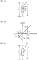
- FIG. 1A is a diagram showing an example of a ferromagnetic tunnel junction device.
- the ferromagnetic tunnel junction device 40 includes a ferromagnetic electrode free layer 42, a ferromagnetic electrode pinned layer 46, and a tunnel insulator 44 interposed between the ferromagnetic electrode free layer 42 and the ferromagnetic electrode pinned layer 46.
- the ferromagnetic electrode free layer 42 and the ferromagnetic electrode pinned layer 46 are made of a ferromagnetic metal, a half-metallic ferromagnet, or a ferromagnetic semiconductor.
- the ferromagnetic electrode free layer 42 has a variable magnetization direction.
- the ferromagnetic electrode pinned layer 46 has a pinned magnetization direction.
- a state where the magnetization directions of the ferromagnetic electrode free layer 42 and the ferromagnetic electrode pinned layer 46 are parallel to each other is referred to as a parallel magnetization, and a state where the magnetization directions are antiparallel to each other is referred to as an antiparallel magnetization.
- FIG. 1B is a diagram showing the current-voltage characteristics of the ferromagnetic tunnel junction device 40.
- a voltage that is applied to the ferromagnetic electrode free layer 42 with respect to the ferromagnetic electrode pinned layer 46 is defined as a voltage V
- a current flowing from the ferromagnetic electrode free layer 42 to the ferromagnetic electrode pinned layer 46 is defined as a current I.
- Symbols in the ferromagnetic tunnel junction device 40 at this point are defined as shown in FIG. 1C . As shown in FIG.
- the resistance Rp of the ferromagnetic tunnel junction device 40 in a parallel magnetization state is lower than the resistance Rap of the ferromagnetic tunnel junction device 40 in an antiparallel magnetization state.
- Rp and Rap are functions of voltages applied to ferromagnetic tunnel junctions, but will be hereinafter regarded as resistances that have approximately constant resistance values. The following discussion applies even to cases where Rp and Rap are not constant resistances.
- the method of reversing the magnetization direction of the ferromagnetic electrode free layer 42 by changing the magnetization direction through spin-polarized charge injection is called a spin-injection magnetization switching method.
- the spin-injection magnetization switching method has a higher possibility of reducing the power consumption required to change a magnetization direction than a method of changing a magnetization direction by generating a magnetic field. Also, unlike the method of changing a magnetization direction by generating a magnetic field, the spin-injection magnetization switching method does not have the problem of leakage magnetic fields. Accordingly, the spin-injection magnetization switching method is hardly affected by disturbances that cause inadvertent writing or erasing in cells other than selected cells, and is suitable for large-scale integration.
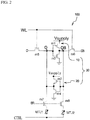
- Fig. 2 is a circuit diagram of the memory cell.
- the memory cell 100 includes a first inverter circuit 10, a second inverter circuit 20, and ferromagnetic tunnel junction devices MTJ1 and MTJ2.
- the first inverter circuit 10 and the second inverter circuit 20 are connected in a ring-like manner, to form a bistable circuit 30.
- the first inverter circuit 10 includes an n-MOSFET (Metal Oxide Semiconductor Field Effect Transistor) m2 and a p-MOSFET m1.
- the second inverter circuit 20 includes an n-MOSFET m4 and a p-MOSFET m3.
- the nodes to which the first inverter circuit 10 and the second inverter circuit 20 are connected are nodes Q and QB.
- the node Q and the node QB are complementary to each other, and the bistable circuit 30 is put into a stable state when the node Q and the node QB are at a high level and a low level, respectively, or when the node Q and the node QB are at a low level and a high level, respectively.
- the bistable circuit 30 is capable of storing data when in a stable state.
- the nodes Q and QB are connected to input/output lines D and DB via MOSFETs m5 and m6, respectively.
- the gates of the MOSFETs m5 and m6 are connected to a word line WL.
- the MOSFETs m1 through m6 form a 6-MOSFET SRAM.
- An FET m7 and the ferromagnetic tunnel junction device MTJ1 are connected between the node Q and a control line CTRL, and an FET m8 and the ferromagnetic tunnel junction device MTJ2 are connected between the node QB and the control line CTRL.
- One of the source and the drain of each of the FETs m7 and m8 is connected to the node Q/QB, and the other one of the source and the drain is connected to the ferromagnetic tunnel junction device MTJ1/MTJ2.
- the gates of the FETs m7 and m8 are connected to a switch line SR.
- Each of the FETs m7 and m8 may be connected between the ferromagnetic tunnel junction device MTJ1/MTJ2 and the control line CTRL. That is, the source and the drain of each of the FETs m7 and m8 are connected in series to the ferromagnetic tunnel junction device MTJ1/MTJ2 between the nodes Q/QB and the control line CTRL. Alternatively, the FETs m7 and m8 may not be provided.
- Data is written into and read from the bistable circuit 30 in the same manner as with a conventional SRAM.
- the word line WL is set at a high level to put the FETs m5 and m6 into a conduction state
- data in the input/output lines D and DB is written into the bistable circuit 30.
- the input/output lines D and DB are put into an equipotential floating state
- the word line WL is set at a high level to put the FETs m5 and m6 into a conduction state. In this manner, data in the bistable circuit 30 can be read out to the input/output lines D and DB.
- Data is held in the bistable circuit 30 by putting the FETs m5 and m6 into a cut-off state.
- the current flowing between the nodes Q and QB and the control line CTRL can be reduced, and power consumption can be lowered.
- FIG. 3 is a timing chart illustrating control of the memory cell.
- the shaded portion indicates a portion in which it is not clear whether the level is high or low.
- a supply voltage Vsupply is supplied, and the control line CTRL and the switch line SR are at a low level in initial condition.
- Data is written into the bistable circuit 30 by setting the word line WL at a high level and setting the input/output lines D and DB at a high and low level, respectively, or at a low and high level, respectively.
- Data is stored from the bistable circuit 30 into the ferromagnetic tunnel junction devices MTJ1 and MTJ2 by setting the switch line SR and the control line CTRL at a high level during a time period T1, and setting the switch line SR and the control line CTRL at a high level and low level, respectively during a time period T2.
- the ferromagnetic tunnel junction devices MTJ1 and MTJ2 When the nodes Q and QB are at a high level and a low level, respectively, the ferromagnetic tunnel junction devices MTJ1 and MTJ2 have a high resistance and a low resistance, respectively, at the end of T2. When the nodes Q and QB are at a low level and a high level, respectively, the ferromagnetic tunnel junction devices MTJ1 and MTJ2 have a low resistance and a high resistance, respectively, at the end of T2. In this manner, data in the bistable circuit 30 is stored into the ferromagnetic tunnel junction devices MTJ1 and MTJ2.
- the supply voltage Vsupply is set at 0 V, to put the memory cell into a shut-down state. As any current does not flow in the memory cell at this point, power consumption can be lowered.
- Data is restored into the bistable circuit 30 from the ferromagnetic tunnel junction devices MTJ1 and MTJ2 by raising the supply voltage Vsupply from 0 V while maintaining the control line CTRL at a low level and the switch line SR at a high level during a time period T3.
- the nodes Q and QB are at a high level and a low level, respectively, at the end of T3.
- the nodes Q and QB are at a low level and a high level, respectively, at the end of T3. In this manner, data stored in the ferromagnetic tunnel junction devices MTJ1 and MTJ2 in a nonvolatile manner is restored into the bistable circuit.
- Data is read from the bistable circuit 30 by setting the word line WL at a high level.
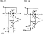
- FIGs. 4A and 4B are circuit diagrams showing other examples of memory cells.
- a resistor R1 can be used in place of the ferromagnetic tunnel junction device MTJ2.
- the node QB and the control line CTRL are not connected to each other.
- the ferromagnetic tunnel junction device may be connected only between one of the nodes Q and QB and the control line CTRL.
- the FET m7 may be connected between the ferromagnetic tunnel junction device MTJ1 and the control line CTRL in each case. Alternatively, the FET m7 may not be provided.
- FIGs. 5A and 5B are block diagrams showing a memory circuit and a memory cell according to a first embodiment.
- a memory circuit 103 includes a memory area 77, a column decoder 71, a column driver 72, a row decoder 73, a row driver 74, and a control unit 85.
- memory cells 100 are arranged in a matrix fashion.
- the column decoder 71 and the row decoder 73 select a column and a row in accordance with an address signal.
- the column driver 72 applies a voltage or the like to the input/output lines D and DB of the selected column and the control line CTRL.
- the row driver 74 applies a voltage or the like to the word line WL of the selected row, the switch line SR, and the control line CTRL.
- the control unit 85 applies a voltage or the like to the input/output lines D and DB, the word line WL, the switch line SR, and the control line CTRL of a memory cell 100, via the column decoder 71, the column driver 72, the row decoder 73, and the row driver 74.
- the memory cells 100 are the same as the memory cell 100 shown in FIG. 2 , for example.
- control line CTRL When the row driver 74 applies a voltage to a control line CTRL, the control line CTRL is connected to each of the memory cells 100 arranged in one row.
- the control line CTRL When the column driver 72 applies a voltage to a control line CTRL, the control line CTRL is collectively connected to the memory cells 100 arranged in a column, for example.
- FIG. 6 is a block diagram of a memory cell and a determining unit according to the first embodiment.
- a memory circuit 101 includes the memory cell 100 shown in Fig. 2 and a determining unit 50.
- the structure of the memory cell 100 is the same as the structure shown in FIG. 5B , and therefore, explanation thereof is not repeated herein.
- the determining unit 50 determines whether the data in the bistable circuit 30 is the same as the data in the ferromagnetic tunnel junction devices MTJ1 and MTJ2 in each memory cell 100.
- the data in the bistable circuit 30 is the same as the data in the ferromagnetic tunnel junction devices MTJ1 and MTJ2.
- the data in the bistable circuit 30 is not the same as the data in the ferromagnetic tunnel junction devices MTJ1 and MTJ2.
- the determining unit 50 outputs a match signal indicating whether the data is the same to the control unit 85.
- the control unit 85 receives a match signal for each memory cell 100 that stores data in a nonvolatile manner among the memory cells 100.
- the match signal indicates that the data is the same, nonvolatile storing is not performed in the memory cell 100.
- the match signal indicates that the data is not the same, nonvolatile storing is performed in the memory cell 100.
- FIGs. 7A and 7B are timing charts of the power supply, the switch line, and the control line.
- the control unit 85 sets the voltage of the switch line SR at a high level (VDD) during a time period in which storing is performed in a memory cell 100 in which the data in the bistable circuit 30 is not the same as the data in the ferromagnetic tunnel junction devices MTJ1 and MTJ2.
- the control unit 85 sets the voltage of the control line CTRL at a low level (0 V) and a high level (VDD). In this manner, the data in the bistable circuit 30 is stored into the ferromagnetic tunnel junction devices MTJ1 and MTJ2. After that, the control unit 85 sets the supply voltage Vsupply at 0 V during a later shut-down period.
- the control unit 85 sets the voltage of the control line CTRL at a low level (0 V) during a time period in which storing is performed in a memory cell 100 in which the data in the bistable circuit 30 is the same as the data in the ferromagnetic tunnel junction devices MTJ1 and MTJ2. As a result, the data in the bistable circuit 30 is not stored into the ferromagnetic tunnel junction devices MTJ1 and MTJ2. After that, the control unit 85 sets the supply voltage Vsupply at 0 V during a shut-down period.
- the control unit 85 when the data in the bistable circuit 30 is the same as the data in the ferromagnetic tunnel junction devices, the control unit 85 does not store the data in the bistable circuit 30 into the ferromagnetic tunnel junction devices.
- the data in the bistable circuit 30 is not the same as the data in the ferromagnetic tunnel junction devices, the data in the bistable circuit 30 is stored into the ferromagnetic tunnel junction devices. As a result, the power consumed by the storing can be reduced.
- a check can be made to determine whether the data in the bistable circuit 30 is to be stored into the ferromagnetic tunnel junction devices.
- the ferromagnetic tunnel junction devices MTJ1 and MTJ2 are connected between the bistable circuit 30 and the control line CTRL.
- some other circuit structure may be used, as long as data can be stored into a nonvolatile element such as a ferromagnetic tunnel junction device in a nonvolatile manner.
- control unit 85 may receive a skip signal from an external circuit.
- the control unit 85 does not determine whether the data in the bistable circuit 30 is the same as the data in the ferromagnetic tunnel junction devices. Accordingly, processing can be performed at a higher speed.
- the external circuit can select a higher processing speed or a reduction in power consumption through the skip signal.
- the control unit 85 can determine whether the data in the bistable circuit 30 is the same as the data in the ferromagnetic tunnel junction device based on the voltage of the control line CTRL when data is written in the bistable circuit 30. As shown in FIGs. 4A and 4B , only one ferromagnetic tunnel junction device may be provided between one of the nodes Q and QB in the bistable circuit 30 and the control line CTRL.
- FIG. 8 is a block diagram of a memory circuit according to the second embodiment.
- the determining unit 50 includes a comparator 52 and an inverter 54.
- the comparator 52 compares the voltage of the control line CTRL with a reference voltage Vref.
- the inverter 53 inverts the output of the comparator 52, and outputs the result as a match signal.
- FIG. 9 is a timing chart of the switch line and the control line.
- the control unit 85 puts the control line CTRL into a floating state, and sets the switch line SR at a high level at time t1.
- the node Q is at a high level
- the ferromagnetic tunnel junction device MTJ1 has a high resistance
- the node QB is at a low level
- the ferromagnetic tunnel junction device MTJ2 has a low resistance, for example.
- the control line CTRL approaches the level of the node QB connected to the low-resistance ferromagnetic tunnel junction device MTJ2. As a result, the control line CTRL enters a relatively low-voltage state, as indicated by the solid line for the control line CTRL in FIG. 9 .
- the control line CTRL enters a relatively high-voltage state, as indicated by the dashed line in FIG. 9 .
- the reference voltage Vref is appropriately selected, so that a check can be made to determine whether the data in the bistable circuit 30 is the same as the data in the ferromagnetic tunnel junction devices based on the voltage of the control line CTRL. In this manner, the control unit 85 can verify the data stored in each storage cell.
- the reference voltage Vref may be Vsupply/2, for example.
- the data in the bistable circuit 30 is stored by changing the resistance values of nonvolatile elements such as ferromagnetic tunnel junction devices.
- the first nonvolatile element (MTJ1) has one end connected to the node Q and the other end connected to the control line CTRL
- the second nonvolatile element (MTJ2) has one end connected to the node QB and the other end connected to the control line CTRL.
- the control unit 85 can determine whether the data in the bistable circuit 30 is the same as the data in the nonvolatile elements based on the voltage of the control line CTRL when data is written in the bistable circuit 30.
- a check can also be made to determine whether the data in the bistable circuit 30 is the same as the data in the nonvolatile element based on the voltage of the control line CTRL.
- FIG. 10 is a block diagram of a memory cell and a determining unit according to the third embodiment.
- the determining unit 50 includes a readout circuit 56 and a determination circuit 58.
- An output Bout of the readout circuit 56 is input to the determination circuit 58.
- the determination circuit 58 outputs a match signal and an error signal to the control unit 85.
- the error signal is a signal indicating whether the data stored in the ferromagnetic tunnel junction devices contradict each other.
- the other aspects of the structure are the same as those shown in FIG. 6 , and therefore, explanation of them is not repeated herein.
- FIG. 11 is a circuit diagram of a memory circuit according to the third embodiment.
- the readout circuit 56 includes a sense amplifier 61 and a buffer 62.
- the sense amplifier 61 reads out data from the bistable circuit 30.
- the buffer 62 holds the data read out by the sense amplifier 61.
- the determination circuit 58 includes MOSFETs m10 through m15, sense amplifiers 65 and 66, inverters 63, 64, and 67, and an XOR circuit 68.
- the MOSFETs m10 through m13 and the inverter 63 electrically connect a control line CTRL1 or CTRL2 connected to the node Q or QB on the high-level side, to the sense amplifier 65 via a connection line CTRL(H).
- the MOSFETs m10 through m13 and the inverter 63 electrically connect the control line CTRL1 or CTRL2 connected to the node Q or QB on the low-level side, to the sense amplifier 66 via a connection line CTRL(L).
- the sense amplifier 65 compares the voltage of the connection line CTRL(H) connected to the high-level node with a reference voltage VrefH. An output of the sense amplifier 65 is output as a match signal via the inverter 67.
- the sense amplifier 66 compares the voltage of the connection line CTRL(L) connected to the low-level node with a reference voltage VrefL. Outputs of the sense amplifiers 65 and 66 are input to the XOR circuit 68. The XOR circuit 68 outputs an error signal.
- the error signal is a signal indicating whether contradictory data are stored in the two ferromagnetic tunnel junction devices. For example, when the ferromagnetic tunnel junction devices MTJ1 and MTJ2 both have a low resistance or both have a high resistance, contradictory data are stored in the two ferromagnetic tunnel junction devices.
- the MOSFETs m14 and m15 and the inverter 64 precharge the connection lines CTRL(H) and CTRL(L).
- FIG. 12 is a timing chart of the respective signals.
- the readout circuit 56 reads out data from the bistable circuit 30.
- the switch line SR and the precharge PC are at a low level.
- the output Bout of the buffer 62 and the connection lines CTRL(H) and CTRL(L) are at a low level or a high level.
- the period from time t2 to time t3 is a precharge period.
- the precharge PC becomes high.
- the connection CTRL(H) and CTRL(L) are precharged at a low level and at a high level, respectively.
- the switch line SR switches to a high level, and the precharge PC switches to a low level.
- the voltage of the connection line CTRL(H) varies as indicated by the solid line when the corresponding ferromagnetic tunnel junction device has a high resistance (when the data is the same).
- the voltage of the connection line CTRL(H) varies as indicated by the dashed line when the corresponding ferromagnetic tunnel junction device has a low resistance (when the data is not the same).
- the voltage of the connection line CTRL(H) is compared with the reference voltage VrefH, so that a check can be made to determine whether the data is the same as the data in the ferromagnetic tunnel junction device corresponding to the high-level node.
- connection line CTRL(L) varies as indicated by the solid line when the corresponding ferromagnetic tunnel junction device has a low resistance (when the data is the same).
- the voltage of the connection line CTRL(L) varies as indicated by the dashed line when the corresponding ferromagnetic tunnel junction device has a high resistance (when the data is not the same).
- the voltage of the connection line CTRL(L) is compared with the reference voltage VrefL, so that a check can be made to determine whether the data is the same as the data in the ferromagnetic tunnel junction device corresponding to the low-level node.
- the control unit 85 can determine whether the data in the bistable circuit 30 is the same as the data in the ferromagnetic tunnel junction devices based on the output Bout of the readout circuit 56 and the voltages of the control lines, as shown in FIG. 10 . For example, a check can be made to determine whether the data is the same, even in a case where only one ferromagnetic tunnel junction device is provided between the node Q or QB in the bistable circuit 30 and the control line CTRL as in FIGs. 4A and 4B .
- the control unit 85 can determine whether the data in the ferromagnetic tunnel junction device MTJ1 and the data in the ferromagnetic tunnel junction device MTJ2 contradict each other based on the output Bout of the readout circuit and the voltages of the control line CTRL1 (the first control line) and the control line CTRL2 (the second control line).
- FIG. 13 is a block diagram showing a memory circuit according to a fourth embodiment.
- the memory circuit 102 includes a memory area 77, a column decoder 71, a column driver 72, a row decoder 73, a row driver 74, determination circuits 75, and a control unit 70.
- memory cells are arranged in a matrix fashion. The memory cells are the same as the memory cell shown in FIG. 2 , FIG. 4A, or FIG. 4B , for example.
- the memory area 77 is divided into regions 76.
- the column decoder 71 and the row decoder 73 select a column and a row in accordance with an address signal.
- the column driver 72 applies a voltage or the like to the input/output lines of the selected column and the control line.
- the row driver 74 applies a voltage or the like to the word line WL of the selected row, the switch line, and the control line.
- Each determination circuit 75 determines whether data in a memory cell in the corresponding region 76 has been rewritten in a volatile manner in a predetermined period of time. For example, data in a memory cell 78 in FIG. 13 has been rewritten in a volatile manner.
- FIG. 14 is a flowchart showing a process to be performed by the control unit at the time of storing.
- the control unit 70 determines whether data in bistable circuits have been rewritten in a volatile manner after data was last restored into a bistable circuit 30 (step S10). If the determination result indicates "Yes”, the control unit 70 stores the data in the bistable circuit 30 into nonvolatile elements (such as ferromagnetic tunnel junction devices) in a nonvolatile manner in each of the memory cells in the region 76 (step S12). If the determination result indicates "No", storing is not performed in the region 76. The control unit 70 determines whether the current region 76 is the last region 76 (step S13). If the determination result indicates "Yes”, the process comes to an end. If the determination result indicates "No”, the process returns to step S10.
- nonvolatile elements such as ferromagnetic tunnel junction devices
- step S12 a check may be made to determine whether to store the data in the bistable circuit 30 into the nonvolatile elements in each memory cell, as in the first through third embodiments.
- the control unit 70 does not store the data in the bistable circuits 30 into the nonvolatile elements, if the data in bistable circuits 30 have not been rewritten in a volatile manner after data was last restored into a bistable circuit 30. If data in at least one of the bistable circuits 30 has been rewritten, on the other hand, the data in the bistable circuit 30 in at least one of the memory cells is stored into the nonvolatile elements. As described above, the data in the bistable circuits 30 are not stored into the nonvolatile elements, if the data in the bistable circuits 30 have not been rewritten in a volatile manner. Accordingly, the power consumed by storing can be reduced.
- the memory cells are divided into the regions 76, and the control unit 70 can determine whether to store the data in the bistable circuits 30 into the nonvolatile elements in each of the regions.
- FIG. 15 is a block diagram showing a memory circuit according to a modification of the fourth embodiment.
- an AND circuit 79 and an SRFF (an SR flip-flop) 80 are provided in place of each of the determination circuits 75 shown in FIG. 13 .
- Each AND circuit 79 performs an AND operation on a rewrite enabling signal EN and a signal indicating whether the memory cell to be rewritten in a volatile manner is located in the corresponding region 76. For example, a check can be made to determine whether the memory cell to be rewritten is located in a specific region 76 in accordance with an address signal.
- the AND circuit 79 outputs a high-level signal when a memory cell in the corresponding region 76 is to be rewritten, and outputs a low-level signal when any of the memory cells in the corresponding region 76 is not to be rewritten.
- Each SRFF 80 stores a high level when a high level is input thereto once. Based on the output of the SRFF 80, the control unit 70 can determine whether a memory cell in the region 76 has been rewritten in a volatile manner in a predetermined period of time. The control unit 70 can reset the output of the SRFF 80 to a low level by using a reset signal RST. For example, when restoring is performed, the determining unit 50 resets the SRFF 80.
- the storage units (the SRFFs 80) store information as to whether the data in at least one of the bistable circuits 30 has been rewritten in each of the regions 76. Accordingly, the control unit 70 can readily determine whether the data in at least one of the bistable circuits 30 has been rewritten.
- the control unit 70 may receive a skip signal from an external circuit.
- the control unit 70 does not determine whether the data in the bistable circuits 30 have been rewritten in a volatile manner after data was last restored into a bistable circuit 30. Accordingly, processing can be performed at a higher speed.
- the external circuit can select a higher processing speed or a reduction in power consumption through the skip signal.
- ferromagnetic tunnel junction devices are used as nonvolatile elements, but some other nonvolatile elements may be used.
- the nonvolatile elements may be variable resistance devices that use CER (Colossal Electro - Resistance) effects used in a ReRAM (Resistive Random Access Memory) or the like.
- the nonvolatile elements may be variable phase devices or ferroelectric devices, for example.
- FIG. 16 is a block diagram of a memory circuit according to the fifth embodiment.
- the memory circuit 104 includes MOSFETs 82 and ferromagnetic tunnel junction devices MTJ that form memory cells 98.
- One of the source and the drain of each MOSFET 82 is connected to a bit line /BL.
- the other one of the source and the drain of each MOSFET 82 is connected to a bit line BL via the corresponding ferromagnetic tunnel junction device MTJ.
- the gate of each MOSFET 82 is connected to a word line WL.
- the memory cells 98 are arranged in a matrix fashion.
- the bit lines /BL and BL are connected to a driver 84.
- the driver 84 writes data into a memory cell 98 in a nonvolatile manner. For example, the driver 84 sets one of the bit lines /BL and BL at a high level, and sets the other one of the bit lines /BL and BL at a low level.
- the word line WL is set at a high level, to put the MOSFET 82 into a conduction state. As a result, a current flows in the ferromagnetic tunnel junction device MTJ.
- the ferromagnetic tunnel junction device MTJ can have a low resistance or a high resistance, as described above with reference to FIGs. 1A through 1C . In this manner, data can be written into the ferromagnetic tunnel junction device in a nonvolatile manner.
- Each bit line /BL is connected to a readout circuit 88.
- the readout circuit 88 reads out data written into a ferromagnetic tunnel junction device MTJ in a nonvolatile manner.
- the bit line BL is set at a high level, and the bit line /BL is put into a floating state.
- the word line WL is set at a high level, to put the MOSFET 82 into a conduction state.
- As the readout circuit 88 detects the potential of the bit line /BL a check can be made to determine whether the ferromagnetic tunnel junction device MTJ has a low resistance or a high resistance. In this manner, data written into the ferromagnetic tunnel junction device MTJ can be read out.
- the read data is output as read data Bout.
- Write data and read data are input to a control unit 86.
- the control unit 86 determines whether the write data and the read data are the same. When the write data and the read data are not the same, the control unit 86 writes the write data into the ferromagnetic tunnel junction device MTJ of the memory cell 98. When the write data and the read data are the same, the control unit 86 does not write the write data into the ferromagnetic tunnel junction device MTJ of the memory cell 98.
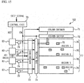
- FIG. 17 is a more specific block diagram of the memory circuit according to the fifth embodiment.
- the readout circuit 88 includes a sense amplifier 94 and a buffer 96.
- the sense amplifier 94 reads out data from a memory cell 98, depending on whether the potential of the corresponding bit line /BL is lower than a reference potential Ref.
- the read data is held in the buffer 96.
- the control unit 86 includes a buffer 90 and an XNOR circuit 92.
- Write data is held in the buffer 90.
- the write data held in the buffer 90 and the read data held in the buffer 96 are input to the XNOR circuit 92.
- the XNOR circuit outputs a high level when the write data and the read data are the same, and outputs a low level when the write data and the read data are not the same.
- the driver 84 When the output of the XNOR circuit 92 is a high level, the driver 84 does not write the write data into the memory cell 98. For example, the driver 84 sets the bit lines /BL and BL at the same potential, or puts the bit lines /BL and BL into a floating state. As a result, any data is not written into the ferromagnetic tunnel junction device MTJ even when the word line WL switches to a high level. When the output of the XNOR circuit 92 is a low level, the write data is written into the memory cell 98.
- the control unit 86 when an output of the readout circuit 88 is the same as the data to be written into a ferromagnetic tunnel junction device MTJ in a nonvolatile manner, the control unit 86 does not write the write data.
- the control unit 86 writes the write data into the ferromagnetic tunnel junction device.
- the power consumed when data is written into a ferromagnetic tunnel junction device MTJ is much larger than the power consumed when data is read out from a ferromagnetic tunnel junction device MTJ. Therefore, when the data written in a ferromagnetic tunnel junction device MTJ is the same as the data to be written into the ferromagnetic tunnel junction device MTJ, the writing is not performed. In this manner, power consumption can be reduced.
- the control unit 86 may receive a skip signal from an external circuit. When receiving a skip signal, the control unit 86 does not determine whether an output of the readout circuit 88 is the same as the data to be written into a ferromagnetic tunnel junction device in a nonvolatile manner. Accordingly, processing can be performed at a higher speed.
- the external circuit can select a higher processing speed or a reduction in power consumption through the skip signal.
- the memory circuits according to the first through fifth embodiments can be used in cache memories, register files, or registers, for example.
- a write operation might be repeated on cells while a check is made to determine (verify) whether writing has been properly performed, so as to avoid wrong writing.
- a check is made to determine (verify) whether data that has already been properly written is the same as the data to be written thereon, which differs from the above mentioned verifying operation. Since the above mentioned verification to avoid wrong writing is normally repeated many times, such a verifying operation is not used in a high-speed memory such as a cache memory.
- the verifying operation to determine whether the data is the same is performed only once for a writing operation. Accordingly, high-speed detection can be performed, and the first through fifth embodiments can be applied to high-speed memories such as a cache memory.
Description
- The present invention relates to memory circuits, and more particularly, to a memory circuit that includes bistable circuits and nonvolatile elements, for example.
- Data written in a bistable circuit of an SRAM (Static Random Access Memory) is stored into a ferromagnetic tunnel junction device (MTJ) in a nonvolatile manner, to cut off the power supply to the bistable circuit. After that, when the bistable circuit is turned on, the data is restored into the bistable circuit from the MTJ (see
Patent Document 1, for example). Power consumption can be reduced by using this memory device in a microprocessor, a system-on-chip, a microcontroller, an FPGA (Field Programmable Gate Array), a CMOS (Complementary Metal Oxide Semiconductor) logic, or the like. -
- Patent Document 1: International Publication Pamphlet
WO 2009/028298 A . - Patent Document 2:
U.S. patent application publication No. 2005/226033 A1 discusses a composite storage circuit and semiconductor device having the same composite storage circuit. - Patent Document 3:
U.S. patent application publication No. 2008/084743 A1 discusses a memory structure capable of bit-wise write or overwrite. - Patent Document 4: Japan patent application publication No.
JP 2010 033620 A - In the memory circuit disclosed in
Patent Document 1, data in a bistable circuit can be stored into an MTJ in a nonvolatile manner, and accordingly, the power supply to the bistable circuit can be cut off. As a result, standby power consumption can be dramatically reduced. While power is being supplied, however, power consumption is larger than that with a conventional SRAM. - The present invention has been made in view of the above problem, and aims to reduce power consumption.
- The present invention is defined by a memory circuit according to
independent claim 1. Preferred aspects are defined in the dependent claims 2-7. - According to the present invention, power consumption can be reduced.
-
-
FIGs. 1A and 1C are diagrams showing an example of a ferromagnetic tunnel junction device, andFIG. 1B is a diagram showing the current-voltage characteristics of the ferromagnetic tunnel junction device; -
FIG. 2 is a circuit diagram of a memory cell; -
FIG. 3 is a timing chart illustrating control of the memory cell; -
FIGs. 4A and 4B are circuit diagrams showing other examples of memory cells; -
FIGs. 5A and 5B are block diagrams showing a memory circuit and a memory cell according to a first embodiment; -
FIG. 6 is a block diagram of a memory cell and a determining unit according to the first embodiment; -
FIGs. 7A and 7B are timing charts of a power supply, a switch line, and a control line; -
FIG. 8 is a block diagram of a memory circuit according to a second embodiment; -
FIG. 9 is a timing chart of a switch line and a control line; -
FIG. 10 is a block diagram of a memory cell and a determining unit according to a third embodiment; -
FIG. 11 is a circuit diagram of a memory circuit according to the third embodiment; -
FIG. 12 is a timing chart of respective signals; -
FIG. 13 is a block diagram of a memory circuit according to a fourth embodiment; -
FIG. 14 is a flowchart showing the process to be performed by the control unit at the time of storing; -
FIG. 15 is a block diagram of a memory circuit according to a modification of the fourth embodiment; -
FIG. 16 is a block diagram of a memory circuit according to a fifth embodiment; and -
FIG. 17 is a more specific block diagram of the memory circuit according to the fifth embodiment. - First, a ferromagnetic tunnel junction device is described as a nonvolatile element.
FIG. 1A is a diagram showing an example of a ferromagnetic tunnel junction device. The ferromagnetictunnel junction device 40 includes a ferromagnetic electrodefree layer 42, a ferromagnetic electrode pinned layer 46, and atunnel insulator 44 interposed between the ferromagnetic electrodefree layer 42 and the ferromagnetic electrode pinned layer 46. The ferromagnetic electrodefree layer 42 and the ferromagnetic electrode pinned layer 46 are made of a ferromagnetic metal, a half-metallic ferromagnet, or a ferromagnetic semiconductor. The ferromagnetic electrodefree layer 42 has a variable magnetization direction. On the other hand, the ferromagnetic electrode pinned layer 46 has a pinned magnetization direction. A state where the magnetization directions of the ferromagnetic electrodefree layer 42 and the ferromagnetic electrode pinned layer 46 are parallel to each other is referred to as a parallel magnetization, and a state where the magnetization directions are antiparallel to each other is referred to as an antiparallel magnetization. -
FIG. 1B is a diagram showing the current-voltage characteristics of the ferromagnetictunnel junction device 40. As shown inFIG. 1A , a voltage that is applied to the ferromagnetic electrodefree layer 42 with respect to the ferromagnetic electrode pinned layer 46 is defined as a voltage V, and a current flowing from the ferromagnetic electrodefree layer 42 to the ferromagnetic electrode pinned layer 46 is defined as a current I. Symbols in the ferromagnetictunnel junction device 40 at this point are defined as shown inFIG. 1C . As shown inFIG. 1B , the resistance Rp of the ferromagnetictunnel junction device 40 in a parallel magnetization state is lower than the resistance Rap of the ferromagnetictunnel junction device 40 in an antiparallel magnetization state. In general, Rp and Rap are functions of voltages applied to ferromagnetic tunnel junctions, but will be hereinafter regarded as resistances that have approximately constant resistance values. The following discussion applies even to cases where Rp and Rap are not constant resistances. - In an antiparallel magnetization state, when the voltage V to be applied to the ferromagnetic
tunnel junction device 40 becomes higher, the current I increases at the rate equivalent to the reciprocal of the resistance Rap (A inFIG. 1B ). When the current I exceeds a threshold current ITF, the magnetization direction of the ferromagnetic electrodefree layer 42 is reversed due to the majority-spin electrons of the ferromagnetic electrode pinned layer 46 injected from the ferromagnetic electrode pinned layer 46 into the ferromagnetic electrodefree layer 42, and a parallel magnetization state appears (B inFIG. 1B ). As a result, the resistance of the ferromagnetictunnel junction device 40 becomes Rp. In a parallel magnetization state, on the other hand, when the negative current I flows (C inFIG. 1B ) and exceeds a threshold current ITR in the negative direction, the minority-spin electrons of the ferromagnetic electrodefree layer 42 among the electrons to be injected from the ferromagnetic electrodefree layer 42 into the ferromagnetic electrode pinned layer 46 are reflected by the ferromagnetic electrode pinned layer 46. As a result, the magnetization direction of the ferromagnetic electrodefree layer 42 is reversed, and an antiparallel magnetization state appears (D inFIG. 1B ). - The method of reversing the magnetization direction of the ferromagnetic electrode
free layer 42 by changing the magnetization direction through spin-polarized charge injection is called a spin-injection magnetization switching method. The spin-injection magnetization switching method has a higher possibility of reducing the power consumption required to change a magnetization direction than a method of changing a magnetization direction by generating a magnetic field. Also, unlike the method of changing a magnetization direction by generating a magnetic field, the spin-injection magnetization switching method does not have the problem of leakage magnetic fields. Accordingly, the spin-injection magnetization switching method is hardly affected by disturbances that cause inadvertent writing or erasing in cells other than selected cells, and is suitable for large-scale integration. - Next, an example of a memory cell that includes a bistable circuit and ferromagnetic tunnel junction devices is described.
Fig. 2 is a circuit diagram of the memory cell. As shown inFig. 2 , thememory cell 100 includes afirst inverter circuit 10, asecond inverter circuit 20, and ferromagnetic tunnel junction devices MTJ1 and MTJ2. Thefirst inverter circuit 10 and thesecond inverter circuit 20 are connected in a ring-like manner, to form abistable circuit 30. Thefirst inverter circuit 10 includes an n-MOSFET (Metal Oxide Semiconductor Field Effect Transistor) m2 and a p-MOSFET m1. Thesecond inverter circuit 20 includes an n-MOSFET m4 and a p-MOSFET m3. - The nodes to which the
first inverter circuit 10 and thesecond inverter circuit 20 are connected are nodes Q and QB. The node Q and the node QB are complementary to each other, and thebistable circuit 30 is put into a stable state when the node Q and the node QB are at a high level and a low level, respectively, or when the node Q and the node QB are at a low level and a high level, respectively. Thebistable circuit 30 is capable of storing data when in a stable state. - The nodes Q and QB are connected to input/output lines D and DB via MOSFETs m5 and m6, respectively. The gates of the MOSFETs m5 and m6 are connected to a word line WL. The MOSFETs m1 through m6 form a 6-MOSFET SRAM.
- An FET m7 and the ferromagnetic tunnel junction device MTJ1 are connected between the node Q and a control line CTRL, and an FET m8 and the ferromagnetic tunnel junction device MTJ2 are connected between the node QB and the control line CTRL. One of the source and the drain of each of the FETs m7 and m8 is connected to the node Q/QB, and the other one of the source and the drain is connected to the ferromagnetic tunnel junction device MTJ1/MTJ2. The gates of the FETs m7 and m8 are connected to a switch line SR. Each of the FETs m7 and m8 may be connected between the ferromagnetic tunnel junction device MTJ1/MTJ2 and the control line CTRL. That is, the source and the drain of each of the FETs m7 and m8 are connected in series to the ferromagnetic tunnel junction device MTJ1/MTJ2 between the nodes Q/QB and the control line CTRL. Alternatively, the FETs m7 and m8 may not be provided.
- Data is written into and read from the
bistable circuit 30 in the same manner as with a conventional SRAM. Specifically, the word line WL is set at a high level to put the FETs m5 and m6 into a conduction state, and data in the input/output lines D and DB is written into thebistable circuit 30. The input/output lines D and DB are put into an equipotential floating state, and the word line WL is set at a high level to put the FETs m5 and m6 into a conduction state. In this manner, data in thebistable circuit 30 can be read out to the input/output lines D and DB. Data is held in thebistable circuit 30 by putting the FETs m5 and m6 into a cut-off state. When data writing, reading, or holding is performed in thebistable circuit 30, it is preferable to set the switch line SR at a low level, and put the FETs m7 and m8 into a cut-off state. As a result, the current flowing between the nodes Q and QB and the control line CTRL can be reduced, and power consumption can be lowered. -
FIG. 3 is a timing chart illustrating control of the memory cell. The shaded portion indicates a portion in which it is not clear whether the level is high or low. As shown inFIG. 3 , a supply voltage Vsupply is supplied, and the control line CTRL and the switch line SR are at a low level in initial condition. Data is written into thebistable circuit 30 by setting the word line WL at a high level and setting the input/output lines D and DB at a high and low level, respectively, or at a low and high level, respectively. Data is stored from thebistable circuit 30 into the ferromagnetic tunnel junction devices MTJ1 and MTJ2 by setting the switch line SR and the control line CTRL at a high level during a time period T1, and setting the switch line SR and the control line CTRL at a high level and low level, respectively during a time period T2. - When the nodes Q and QB are at a high level and a low level, respectively, the ferromagnetic tunnel junction devices MTJ1 and MTJ2 have a high resistance and a low resistance, respectively, at the end of T2. When the nodes Q and QB are at a low level and a high level, respectively, the ferromagnetic tunnel junction devices MTJ1 and MTJ2 have a low resistance and a high resistance, respectively, at the end of T2. In this manner, data in the
bistable circuit 30 is stored into the ferromagnetic tunnel junction devices MTJ1 and MTJ2. - After that, the supply voltage Vsupply is set at 0 V, to put the memory cell into a shut-down state. As any current does not flow in the memory cell at this point, power consumption can be lowered. Data is restored into the
bistable circuit 30 from the ferromagnetic tunnel junction devices MTJ1 and MTJ2 by raising the supply voltage Vsupply from 0 V while maintaining the control line CTRL at a low level and the switch line SR at a high level during a time period T3. - When the ferromagnetic tunnel junction devices MTJ1 and MTJ2 have a high resistance and a low resistance, respectively, the nodes Q and QB are at a high level and a low level, respectively, at the end of T3. When the ferromagnetic tunnel junction devices MTJ1 and MTJ2 have a low resistance and a high resistance, respectively, the nodes Q and QB are at a low level and a high level, respectively, at the end of T3. In this manner, data stored in the ferromagnetic tunnel junction devices MTJ1 and MTJ2 in a nonvolatile manner is restored into the bistable circuit.
- Data is read from the
bistable circuit 30 by setting the word line WL at a high level. -
FIGs. 4A and 4B are circuit diagrams showing other examples of memory cells. As shown inFIG. 4A , a resistor R1 can be used in place of the ferromagnetic tunnel junction device MTJ2. As shown inFIG. 4B , the node QB and the control line CTRL are not connected to each other. As shown inFIGs. 4A and 4B , the ferromagnetic tunnel junction device may be connected only between one of the nodes Q and QB and the control line CTRL. The FET m7 may be connected between the ferromagnetic tunnel junction device MTJ1 and the control line CTRL in each case. Alternatively, the FET m7 may not be provided. -
FIGs. 5A and 5B are block diagrams showing a memory circuit and a memory cell according to a first embodiment. As shown inFIG. 5A , amemory circuit 103 includes amemory area 77, acolumn decoder 71, acolumn driver 72, arow decoder 73, arow driver 74, and acontrol unit 85. In thememory area 77,memory cells 100 are arranged in a matrix fashion. Thecolumn decoder 71 and therow decoder 73 select a column and a row in accordance with an address signal. Thecolumn driver 72 applies a voltage or the like to the input/output lines D and DB of the selected column and the control line CTRL. Therow driver 74 applies a voltage or the like to the word line WL of the selected row, the switch line SR, and the control line CTRL. Thecontrol unit 85 applies a voltage or the like to the input/output lines D and DB, the word line WL, the switch line SR, and the control line CTRL of amemory cell 100, via thecolumn decoder 71, thecolumn driver 72, therow decoder 73, and therow driver 74. As shown inFIG. 5B , thememory cells 100 are the same as thememory cell 100 shown inFIG. 2 , for example. - When the
row driver 74 applies a voltage to a control line CTRL, the control line CTRL is connected to each of thememory cells 100 arranged in one row. When thecolumn driver 72 applies a voltage to a control line CTRL, the control line CTRL is collectively connected to thememory cells 100 arranged in a column, for example. -
FIG. 6 is a block diagram of a memory cell and a determining unit according to the first embodiment. As shown inFig. 6 , amemory circuit 101 includes thememory cell 100 shown inFig. 2 and a determiningunit 50. The structure of thememory cell 100 is the same as the structure shown inFIG. 5B , and therefore, explanation thereof is not repeated herein. When data is written intomemory cells 100 in a nonvolatile manner, the determiningunit 50 determines whether the data in thebistable circuit 30 is the same as the data in the ferromagnetic tunnel junction devices MTJ1 and MTJ2 in eachmemory cell 100. For example, when the nodes Q and QB are at a high level and a low level, respectively, and the ferromagnetic tunnel junction devices MTJ1 and MTJ2 have a high resistance and a low resistance, respectively, the data in thebistable circuit 30 is the same as the data in the ferromagnetic tunnel junction devices MTJ1 and MTJ2. When the nodes Q and QB are at a high level and a low level, respectively, and the ferromagnetic tunnel junction devices MTJ1 and MTJ2 have a low resistance and a high resistance, respectively, the data in thebistable circuit 30 is not the same as the data in the ferromagnetic tunnel junction devices MTJ1 and MTJ2. The determiningunit 50 outputs a match signal indicating whether the data is the same to thecontrol unit 85. - The
control unit 85 receives a match signal for eachmemory cell 100 that stores data in a nonvolatile manner among thememory cells 100. When the match signal indicates that the data is the same, nonvolatile storing is not performed in thememory cell 100. When the match signal indicates that the data is not the same, nonvolatile storing is performed in thememory cell 100. -
FIGs. 7A and 7B are timing charts of the power supply, the switch line, and the control line. As shown inFIG. 7A , thecontrol unit 85 sets the voltage of the switch line SR at a high level (VDD) during a time period in which storing is performed in amemory cell 100 in which the data in thebistable circuit 30 is not the same as the data in the ferromagnetic tunnel junction devices MTJ1 and MTJ2. Thecontrol unit 85 sets the voltage of the control line CTRL at a low level (0 V) and a high level (VDD). In this manner, the data in thebistable circuit 30 is stored into the ferromagnetic tunnel junction devices MTJ1 and MTJ2. After that, thecontrol unit 85 sets the supply voltage Vsupply at 0 V during a later shut-down period. - As shown in
FIG. 7B , thecontrol unit 85 sets the voltage of the control line CTRL at a low level (0 V) during a time period in which storing is performed in amemory cell 100 in which the data in thebistable circuit 30 is the same as the data in the ferromagnetic tunnel junction devices MTJ1 and MTJ2. As a result, the data in thebistable circuit 30 is not stored into the ferromagnetic tunnel junction devices MTJ1 and MTJ2. After that, thecontrol unit 85 sets the supply voltage Vsupply at 0 V during a shut-down period. - According to the first embodiment, when the data in the
bistable circuit 30 is the same as the data in the ferromagnetic tunnel junction devices, thecontrol unit 85 does not store the data in thebistable circuit 30 into the ferromagnetic tunnel junction devices. When the data in thebistable circuit 30 is not the same as the data in the ferromagnetic tunnel junction devices, the data in thebistable circuit 30 is stored into the ferromagnetic tunnel junction devices. As a result, the power consumed by the storing can be reduced. As described above, in each of thememory cells 100, a check can be made to determine whether the data in thebistable circuit 30 is to be stored into the ferromagnetic tunnel junction devices. In the first embodiment, the ferromagnetic tunnel junction devices MTJ1 and MTJ2 are connected between thebistable circuit 30 and the control line CTRL. However, some other circuit structure may be used, as long as data can be stored into a nonvolatile element such as a ferromagnetic tunnel junction device in a nonvolatile manner. - Also, the
control unit 85 may receive a skip signal from an external circuit. When receiving a skip signal, thecontrol unit 85 does not determine whether the data in thebistable circuit 30 is the same as the data in the ferromagnetic tunnel junction devices. Accordingly, processing can be performed at a higher speed. The external circuit can select a higher processing speed or a reduction in power consumption through the skip signal. - In a case where the data in the
bistable circuit 30 is stored by changing the resistance value of a nonvolatile element such as a ferromagnetic tunnel junction device, thecontrol unit 85 can determine whether the data in thebistable circuit 30 is the same as the data in the ferromagnetic tunnel junction device based on the voltage of the control line CTRL when data is written in thebistable circuit 30. As shown inFIGs. 4A and 4B , only one ferromagnetic tunnel junction device may be provided between one of the nodes Q and QB in thebistable circuit 30 and the control line CTRL. - A second embodiment is a specific example of the first embodiment.
FIG. 8 is a block diagram of a memory circuit according to the second embodiment. As shown inFIG. 8 , the determiningunit 50 includes acomparator 52 and aninverter 54. Thecomparator 52 compares the voltage of the control line CTRL with a reference voltage Vref. The inverter 53 inverts the output of thecomparator 52, and outputs the result as a match signal. -
FIG. 9 is a timing chart of the switch line and the control line. Thecontrol unit 85 puts the control line CTRL into a floating state, and sets the switch line SR at a high level at time t1. When the data in thebistable circuit 30 is the same as the data in the ferromagnetic tunnel junction devices, the node Q is at a high level, the ferromagnetic tunnel junction device MTJ1 has a high resistance, the node QB is at a low level, and the ferromagnetic tunnel junction device MTJ2 has a low resistance, for example. The control line CTRL approaches the level of the node QB connected to the low-resistance ferromagnetic tunnel junction device MTJ2. As a result, the control line CTRL enters a relatively low-voltage state, as indicated by the solid line for the control line CTRL inFIG. 9 . - When the data in the
bistable circuit 30 is not the same as the data in the ferromagnetic tunnel junction devices, on the other hand, the node connected to the low-resistance ferromagnetic tunnel junction device is at a high level. As a result, the control line CTRL enters a relatively high-voltage state, as indicated by the dashed line inFIG. 9 . In view of this, the reference voltage Vref is appropriately selected, so that a check can be made to determine whether the data in thebistable circuit 30 is the same as the data in the ferromagnetic tunnel junction devices based on the voltage of the control line CTRL. In this manner, thecontrol unit 85 can verify the data stored in each storage cell. The reference voltage Vref may be Vsupply/2, for example. - In the second embodiment, the data in the
bistable circuit 30 is stored by changing the resistance values of nonvolatile elements such as ferromagnetic tunnel junction devices. The first nonvolatile element (MTJ1) has one end connected to the node Q and the other end connected to the control line CTRL, and the second nonvolatile element (MTJ2) has one end connected to the node QB and the other end connected to the control line CTRL. In this case, thecontrol unit 85 can determine whether the data in thebistable circuit 30 is the same as the data in the nonvolatile elements based on the voltage of the control line CTRL when data is written in thebistable circuit 30. In a case where only one ferromagnetic tunnel junction device is provided between one of the nodes Q and WB and the control line CTRL as inFIGs. 4A and 4B , a check can also be made to determine whether the data in thebistable circuit 30 is the same as the data in the nonvolatile element based on the voltage of the control line CTRL. - A third embodiment is another specific example of the first embodiment.
FIG. 10 is a block diagram of a memory cell and a determining unit according to the third embodiment. As shown inFIG. 10 , the determiningunit 50 includes areadout circuit 56 and adetermination circuit 58. An output Bout of thereadout circuit 56 is input to thedetermination circuit 58. Thedetermination circuit 58 outputs a match signal and an error signal to thecontrol unit 85. The error signal is a signal indicating whether the data stored in the ferromagnetic tunnel junction devices contradict each other. The other aspects of the structure are the same as those shown inFIG. 6 , and therefore, explanation of them is not repeated herein. -
FIG. 11 is a circuit diagram of a memory circuit according to the third embodiment. As shown inFIG. 11 , thereadout circuit 56 includes asense amplifier 61 and abuffer 62. Thesense amplifier 61 reads out data from thebistable circuit 30. Thebuffer 62 holds the data read out by thesense amplifier 61. - The
determination circuit 58 includes MOSFETs m10 through m15,sense amplifiers inverters XOR circuit 68. The MOSFETs m10 through m13 and theinverter 63 electrically connect a control line CTRL1 or CTRL2 connected to the node Q or QB on the high-level side, to thesense amplifier 65 via a connection line CTRL(H). Also, the MOSFETs m10 through m13 and theinverter 63 electrically connect the control line CTRL1 or CTRL2 connected to the node Q or QB on the low-level side, to thesense amplifier 66 via a connection line CTRL(L). Thesense amplifier 65 compares the voltage of the connection line CTRL(H) connected to the high-level node with a reference voltage VrefH. An output of thesense amplifier 65 is output as a match signal via theinverter 67. - The
sense amplifier 66 compares the voltage of the connection line CTRL(L) connected to the low-level node with a reference voltage VrefL. Outputs of thesense amplifiers XOR circuit 68. TheXOR circuit 68 outputs an error signal. The error signal is a signal indicating whether contradictory data are stored in the two ferromagnetic tunnel junction devices. For example, when the ferromagnetic tunnel junction devices MTJ1 and MTJ2 both have a low resistance or both have a high resistance, contradictory data are stored in the two ferromagnetic tunnel junction devices. The MOSFETs m14 and m15 and theinverter 64 precharge the connection lines CTRL(H) and CTRL(L). -
FIG. 12 is a timing chart of the respective signals. Thereadout circuit 56 reads out data from thebistable circuit 30. At this point, the switch line SR and the precharge PC are at a low level. The output Bout of thebuffer 62 and the connection lines CTRL(H) and CTRL(L) are at a low level or a high level. The period from time t2 to time t3 is a precharge period. The precharge PC becomes high. The connection CTRL(H) and CTRL(L) are precharged at a low level and at a high level, respectively. - At time t3, the switch line SR switches to a high level, and the precharge PC switches to a low level. The voltage of the connection line CTRL(H) varies as indicated by the solid line when the corresponding ferromagnetic tunnel junction device has a high resistance (when the data is the same). The voltage of the connection line CTRL(H) varies as indicated by the dashed line when the corresponding ferromagnetic tunnel junction device has a low resistance (when the data is not the same). At time t4, the voltage of the connection line CTRL(H) is compared with the reference voltage VrefH, so that a check can be made to determine whether the data is the same as the data in the ferromagnetic tunnel junction device corresponding to the high-level node. The voltage of the connection line CTRL(L) varies as indicated by the solid line when the corresponding ferromagnetic tunnel junction device has a low resistance (when the data is the same). The voltage of the connection line CTRL(L) varies as indicated by the dashed line when the corresponding ferromagnetic tunnel junction device has a high resistance (when the data is not the same). At time t4, the voltage of the connection line CTRL(L) is compared with the reference voltage VrefL, so that a check can be made to determine whether the data is the same as the data in the ferromagnetic tunnel junction device corresponding to the low-level node.
- According to the third embodiment, the
control unit 85 can determine whether the data in thebistable circuit 30 is the same as the data in the ferromagnetic tunnel junction devices based on the output Bout of thereadout circuit 56 and the voltages of the control lines, as shown inFIG. 10 . For example, a check can be made to determine whether the data is the same, even in a case where only one ferromagnetic tunnel junction device is provided between the node Q or QB in thebistable circuit 30 and the control line CTRL as inFIGs. 4A and 4B . - Also, in a case where the two ferromagnetic tunnel junction devices MTJ1 and MTJ2 are connected between the two nodes Q and QB in the
bistable circuit 30 and the connection lines CTRL(H) and CTRL(L), respectively, thecontrol unit 85 can determine whether the data in the ferromagnetic tunnel junction device MTJ1 and the data in the ferromagnetic tunnel junction device MTJ2 contradict each other based on the output Bout of the readout circuit and the voltages of the control line CTRL1 (the first control line) and the control line CTRL2 (the second control line). -
FIG. 13 is a block diagram showing a memory circuit according to a fourth embodiment. As shown inFIG. 13 , thememory circuit 102 includes amemory area 77, acolumn decoder 71, acolumn driver 72, arow decoder 73, arow driver 74,determination circuits 75, and acontrol unit 70. In thememory area 77, memory cells are arranged in a matrix fashion. The memory cells are the same as the memory cell shown inFIG. 2 ,FIG. 4A, or FIG. 4B , for example. Thememory area 77 is divided intoregions 76. Thecolumn decoder 71 and therow decoder 73 select a column and a row in accordance with an address signal. Thecolumn driver 72 applies a voltage or the like to the input/output lines of the selected column and the control line. Therow driver 74 applies a voltage or the like to the word line WL of the selected row, the switch line, and the control line. Eachdetermination circuit 75 determines whether data in a memory cell in thecorresponding region 76 has been rewritten in a volatile manner in a predetermined period of time. For example, data in amemory cell 78 inFIG. 13 has been rewritten in a volatile manner. -
FIG. 14 is a flowchart showing a process to be performed by the control unit at the time of storing. As shown inFIG. 14 , at the time of storing, thecontrol unit 70 determines whether data in bistable circuits have been rewritten in a volatile manner after data was last restored into a bistable circuit 30 (step S10). If the determination result indicates "Yes", thecontrol unit 70 stores the data in thebistable circuit 30 into nonvolatile elements (such as ferromagnetic tunnel junction devices) in a nonvolatile manner in each of the memory cells in the region 76 (step S12). If the determination result indicates "No", storing is not performed in theregion 76. Thecontrol unit 70 determines whether thecurrent region 76 is the last region 76 (step S13). If the determination result indicates "Yes", the process comes to an end. If the determination result indicates "No", the process returns to step S10. - In step S12, a check may be made to determine whether to store the data in the
bistable circuit 30 into the nonvolatile elements in each memory cell, as in the first through third embodiments. - According to the fourth embodiment, the
control unit 70 does not store the data in thebistable circuits 30 into the nonvolatile elements, if the data inbistable circuits 30 have not been rewritten in a volatile manner after data was last restored into abistable circuit 30. If data in at least one of thebistable circuits 30 has been rewritten, on the other hand, the data in thebistable circuit 30 in at least one of the memory cells is stored into the nonvolatile elements. As described above, the data in thebistable circuits 30 are not stored into the nonvolatile elements, if the data in thebistable circuits 30 have not been rewritten in a volatile manner. Accordingly, the power consumed by storing can be reduced. - Furthermore, the memory cells are divided into the
regions 76, and thecontrol unit 70 can determine whether to store the data in thebistable circuits 30 into the nonvolatile elements in each of the regions. -
FIG. 15 is a block diagram showing a memory circuit according to a modification of the fourth embodiment. As shown inFIG. 15 , for each of theregions 76, an ANDcircuit 79 and an SRFF (an SR flip-flop) 80 are provided in place of each of thedetermination circuits 75 shown inFIG. 13 . Each ANDcircuit 79 performs an AND operation on a rewrite enabling signal EN and a signal indicating whether the memory cell to be rewritten in a volatile manner is located in thecorresponding region 76. For example, a check can be made to determine whether the memory cell to be rewritten is located in aspecific region 76 in accordance with an address signal. The ANDcircuit 79 outputs a high-level signal when a memory cell in thecorresponding region 76 is to be rewritten, and outputs a low-level signal when any of the memory cells in thecorresponding region 76 is not to be rewritten. EachSRFF 80 stores a high level when a high level is input thereto once. Based on the output of theSRFF 80, thecontrol unit 70 can determine whether a memory cell in theregion 76 has been rewritten in a volatile manner in a predetermined period of time. Thecontrol unit 70 can reset the output of theSRFF 80 to a low level by using a reset signal RST. For example, when restoring is performed, the determiningunit 50 resets theSRFF 80. - As in the modification of the fourth embodiment, the storage units (the SRFFs 80) store information as to whether the data in at least one of the
bistable circuits 30 has been rewritten in each of theregions 76. Accordingly, thecontrol unit 70 can readily determine whether the data in at least one of thebistable circuits 30 has been rewritten. - In the fourth embodiment and the modification thereof, the
control unit 70 may receive a skip signal from an external circuit. When receiving a skip signal, thecontrol unit 70 does not determine whether the data in thebistable circuits 30 have been rewritten in a volatile manner after data was last restored into abistable circuit 30. Accordingly, processing can be performed at a higher speed. The external circuit can select a higher processing speed or a reduction in power consumption through the skip signal. - In the above described first through fourth embodiments and the modifications thereof, ferromagnetic tunnel junction devices are used as nonvolatile elements, but some other nonvolatile elements may be used. For example, the nonvolatile elements may be variable resistance devices that use CER (Colossal Electro - Resistance) effects used in a ReRAM (Resistive Random Access Memory) or the like. Also, the nonvolatile elements may be variable phase devices or ferroelectric devices, for example.
- A fifth embodiment is an example of an MRAM (Magnetic Random Access Memory).
FIG. 16 is a block diagram of a memory circuit according to the fifth embodiment. Thememory circuit 104 includesMOSFETs 82 and ferromagnetic tunnel junction devices MTJ that formmemory cells 98. One of the source and the drain of eachMOSFET 82 is connected to a bit line /BL. The other one of the source and the drain of eachMOSFET 82 is connected to a bit line BL via the corresponding ferromagnetic tunnel junction device MTJ. The gate of eachMOSFET 82 is connected to a word line WL. Thememory cells 98 are arranged in a matrix fashion. - The bit lines /BL and BL are connected to a
driver 84. Thedriver 84 writes data into amemory cell 98 in a nonvolatile manner. For example, thedriver 84 sets one of the bit lines /BL and BL at a high level, and sets the other one of the bit lines /BL and BL at a low level. The word line WL is set at a high level, to put theMOSFET 82 into a conduction state. As a result, a current flows in the ferromagnetic tunnel junction device MTJ. Depending on the direction of the current flowing in the ferromagnetic tunnel junction device MTJ, the ferromagnetic tunnel junction device MTJ can have a low resistance or a high resistance, as described above with reference toFIGs. 1A through 1C . In this manner, data can be written into the ferromagnetic tunnel junction device in a nonvolatile manner. - Each bit line /BL is connected to a
readout circuit 88. Thereadout circuit 88 reads out data written into a ferromagnetic tunnel junction device MTJ in a nonvolatile manner. The bit line BL is set at a high level, and the bit line /BL is put into a floating state. The word line WL is set at a high level, to put theMOSFET 82 into a conduction state. As thereadout circuit 88 detects the potential of the bit line /BL, a check can be made to determine whether the ferromagnetic tunnel junction device MTJ has a low resistance or a high resistance. In this manner, data written into the ferromagnetic tunnel junction device MTJ can be read out. The read data is output as read data Bout. - Write data and read data are input to a
control unit 86. Thecontrol unit 86 determines whether the write data and the read data are the same. When the write data and the read data are not the same, thecontrol unit 86 writes the write data into the ferromagnetic tunnel junction device MTJ of thememory cell 98. When the write data and the read data are the same, thecontrol unit 86 does not write the write data into the ferromagnetic tunnel junction device MTJ of thememory cell 98. -
FIG. 17 is a more specific block diagram of the memory circuit according to the fifth embodiment. Thereadout circuit 88 includes asense amplifier 94 and abuffer 96. Thesense amplifier 94 reads out data from amemory cell 98, depending on whether the potential of the corresponding bit line /BL is lower than a reference potential Ref. The read data is held in thebuffer 96. Thecontrol unit 86 includes abuffer 90 and anXNOR circuit 92. Write data is held in thebuffer 90. The write data held in thebuffer 90 and the read data held in thebuffer 96 are input to theXNOR circuit 92. The XNOR circuit outputs a high level when the write data and the read data are the same, and outputs a low level when the write data and the read data are not the same. When the output of theXNOR circuit 92 is a high level, thedriver 84 does not write the write data into thememory cell 98. For example, thedriver 84 sets the bit lines /BL and BL at the same potential, or puts the bit lines /BL and BL into a floating state. As a result, any data is not written into the ferromagnetic tunnel junction device MTJ even when the word line WL switches to a high level. When the output of theXNOR circuit 92 is a low level, the write data is written into thememory cell 98. - According to the fifth embodiment, when an output of the
readout circuit 88 is the same as the data to be written into a ferromagnetic tunnel junction device MTJ in a nonvolatile manner, thecontrol unit 86 does not write the write data. When the output of thereadout circuit 88 is not the same as the data to be written in a nonvolatile manner, on the other hand, thecontrol unit 86 writes the write data into the ferromagnetic tunnel junction device. The power consumed when data is written into a ferromagnetic tunnel junction device MTJ is much larger than the power consumed when data is read out from a ferromagnetic tunnel junction device MTJ. Therefore, when the data written in a ferromagnetic tunnel junction device MTJ is the same as the data to be written into the ferromagnetic tunnel junction device MTJ, the writing is not performed. In this manner, power consumption can be reduced. - The
control unit 86 may receive a skip signal from an external circuit. When receiving a skip signal, thecontrol unit 86 does not determine whether an output of thereadout circuit 88 is the same as the data to be written into a ferromagnetic tunnel junction device in a nonvolatile manner. Accordingly, processing can be performed at a higher speed. The external circuit can select a higher processing speed or a reduction in power consumption through the skip signal. - Although a voltage sense amplifier is used in reading out data in the above described first through fifth embodiments, it is also possible to use a current sense amplifier.
- The memory circuits according to the first through fifth embodiments can be used in cache memories, register files, or registers, for example. In a case where write conditions are very strict when data is written into a nonvolatile memory such as a flash memory, a write operation might be repeated on cells while a check is made to determine (verify) whether writing has been properly performed, so as to avoid wrong writing. In the memory circuits of the first through fifth embodiments, a check is made to determine (verify) whether data that has already been properly written is the same as the data to be written thereon, which differs from the above mentioned verifying operation. Since the above mentioned verification to avoid wrong writing is normally repeated many times, such a verifying operation is not used in a high-speed memory such as a cache memory. In the memory circuits of the first through fifth embodiments, on the other hand, the verifying operation to determine whether the data is the same is performed only once for a writing operation. Accordingly, high-speed detection can be performed, and the first through fifth embodiments can be applied to high-speed memories such as a cache memory.
- Although preferred embodiments of the present invention have been described so far, the present invention is not limited to those particular embodiments, and various changes and modifications may be made to them within the scope of the appended claims 1-7.
-
- 10, 20
- inverter
- 30
- bistable circuit
- 70, 85, 86
- control unit
- MTJ1, MTJ2
- ferromagnetic tunnel junction device
Claims (7)
- A memory circuit comprising:
a memory area (77) in which a plurality of memory cells (100) are arranged in matrix fashion in a plurality of rows and columns, each of the plurality of memory cells (100) including a bistable circuit (30) configured to write data in a volatile manner, and a nonvolatile element (MTJ1, MTJ2) configured to store the data written in the bistable circuit (30) in a nonvolatile manner and restore the data stored in a nonvolatile manner into the bistable circuit (30);
characterized in that the memory circuit further comprises:a control line (CTRL) directly connected to the nonvolatile element (MTJ1, MTJ2) of each of a plurality of memory cells arranged in one of a row and a column, wherein the nonvolatile element (MTJ1, MTJ2) has one end connected to a node (Q, QB) in the bistable circuit (30) and has the other end directly connected to the control line (CTRL);a determining unit (50) configured to determine that the data in the bistable circuit (30) is the same as the data in the nonvolatile element (MTJ1, MTJ2) in each memory cell of the plurality of memory cells arranged in the one of the row and the column when a voltage of the control line (CTRL) is lower than a reference voltage, and to determine that the data in the bistable circuit (30) is not the same as the data in the nonvolatile element (MTJ1, MTJ2) in each memory cell of the plurality of memory cells arranged in the one of the row and the column when the voltage of the control line (CTRL) is higher than the reference voltage; anda control unit (85) located outside the memory area (77) configured to apply, during a time period in which storing is performed in a memory cell, a low level voltage to the control line (CTRL) when the determining unit (50) determines that the data in the bistable circuit (30) is the same as the data in the nonvolatile element (MTJ1, MTJ2), and configured to apply, during the time period in which storing is performed in the memory cell, the low level voltage during part of said time period and a high level voltage during another part of said time period to the control line (CTRL) when the determining unit determines that the data in the bistable circuit (30) is not the same as the data in the non-volatile element (MTJ1, MTJ2). - The memory circuit according to claim 1, wherein
the nonvolatile element (MTJ1, MTJ2) is configured to store the data in the bistable circuit (30) by changing the resistance value thereof. - The memory circuit according to claim 1, wherein
the bistable circuit (30) includes a first node (Q) and a second node (QB), the first node (Q) and the second node (QB) being complementary to each other, and
the nonvolatile element includes a first nonvolatile element (MTJ1) and a second nonvolatile element (MTJ2), the first nonvolatile element (MTJ1) having one end connected to the first node (Q) and the other end connected to the control line (CTRL), the second nonvolatile element (MTJ2) having one end connected to the second node (QB) and the other end connected to the control line (CTRL). - The memory circuit according to claim 1, further comprising
a readout circuit (56) configured to read out the data from the bistable circuit (30),
wherein the control unit (85) is further configured to determine whether the data in the bistable circuit (30) is the same as the data in the nonvolatile element (MTJ1, MTJ2) based on an output of the readout circuit (56) and the voltage of the control line (CTRL). - The memory circuit according to claim 4, wherein
the bistable circuit (30) includes a first node (Q) and a second node (QB), the first node (Q) and the second node (QB) being complementary to each other,
the control line includes a first control line (CTRL1) and a second control line (CTRL2),
the nonvolatile element includes a first nonvolatile element (MTJ1) and a second nonvolatile element (MTJ2), the first nonvolatile element (MTJ1) having one end connected to the first node (Q) and the other end connected to the first control line (CTRL1), the second nonvolatile element (MTJ2) having one end connected to the second node (QB) and the other end connected to the second control line (CTRL2), and
the control unit (85) is further configured to determine that data in the first nonvolatile element (MTJ1) and data in the second nonvolatile element (MTJ2) contradict when both of the first nonvolatile element (MTJ1) and the second nonvolatile element (MTJ2) have a low resistance or a high resistance. - The memory circuit according to any one of claims 1 through 5, wherein the control unit (85) is further configured to: when receiving a skip signal, controlling the determining unit (50) to not determine whether the data in the bistable circuit (30) is the same as the data in the nonvolatile element (MTJ1, MTJ2).
- The memory circuit according to any one of claims 1 through 6, wherein the nonvolatile element (MTJ1, MTJ2) is a ferromagnetic tunnel junction device (MTJ1, MTJ2).
Applications Claiming Priority (3)
| Application Number | Priority Date | Filing Date | Title |
|---|---|---|---|
| JP2012114988 | 2012-05-18 | ||
| PCT/JP2013/054051 WO2013172065A1 (en) | 2012-05-18 | 2013-02-19 | Memory circuit |
| EP13791432.1A EP2840575B1 (en) | 2012-05-18 | 2013-02-19 | Memory circuit |
Related Parent Applications (2)
| Application Number | Title | Priority Date | Filing Date |
|---|---|---|---|
| EP13791432.1A Division-Into EP2840575B1 (en) | 2012-05-18 | 2013-02-19 | Memory circuit |
| EP13791432.1A Division EP2840575B1 (en) | 2012-05-18 | 2013-02-19 | Memory circuit |
Publications (2)
| Publication Number | Publication Date |
|---|---|
| EP3107105A1 EP3107105A1 (en) | 2016-12-21 |
| EP3107105B1 true EP3107105B1 (en) | 2021-06-16 |
Family
ID=49583490
Family Applications (3)
| Application Number | Title | Priority Date | Filing Date |
|---|---|---|---|
| EP16181451.2A Active EP3107105B1 (en) | 2012-05-18 | 2013-02-19 | Memory circuit |
| EP13791432.1A Active EP2840575B1 (en) | 2012-05-18 | 2013-02-19 | Memory circuit |
| EP16180034.7A Active EP3109863B1 (en) | 2012-05-18 | 2013-02-19 | Memory circuit |
Family Applications After (2)
| Application Number | Title | Priority Date | Filing Date |
|---|---|---|---|
| EP13791432.1A Active EP2840575B1 (en) | 2012-05-18 | 2013-02-19 | Memory circuit |
| EP16180034.7A Active EP3109863B1 (en) | 2012-05-18 | 2013-02-19 | Memory circuit |
Country Status (7)
| Country | Link |
|---|---|
| US (1) | US9496037B2 (en) |
| EP (3) | EP3107105B1 (en) |
| JP (1) | JP5479656B1 (en) |
| KR (1) | KR101666537B1 (en) |
| CN (1) | CN104303234B (en) |
| TW (1) | TWI582764B (en) |
| WO (1) | WO2013172065A1 (en) |
Families Citing this family (9)
| Publication number | Priority date | Publication date | Assignee | Title |
|---|---|---|---|---|
| JP6372203B2 (en) * | 2014-07-07 | 2018-08-15 | 株式会社ソシオネクスト | Data holding circuit and held data restoring method |
| WO2016024527A1 (en) * | 2014-08-12 | 2016-02-18 | 国立研究開発法人科学技術振興機構 | Memory circuit |
| US10373677B2 (en) | 2015-06-24 | 2019-08-06 | Sony Corporation | Semiconductor device to reduce energy consumed to write data |
| US9805795B2 (en) * | 2016-01-08 | 2017-10-31 | Samsung Electronics Co., Ltd. | Zero leakage, high noise margin coupled giant spin hall based retention latch |
| DE112017001059T5 (en) | 2016-02-29 | 2018-11-29 | Sony Corporation | SEMICONDUCTOR CIRCUIT, METHOD FOR CONTROLLING THE SEMICONDUCTOR CIRCUIT AND ELECTRONIC DEVICE |
| US10476456B2 (en) * | 2016-10-04 | 2019-11-12 | Mediatek Inc. | Comparator having a high-speed amplifier and a low-noise amplifier |
| JP7007173B2 (en) * | 2016-12-16 | 2022-01-24 | ソニーセミコンダクタソリューションズ株式会社 | Semiconductor device |
| JP6734904B2 (en) * | 2018-11-01 | 2020-08-05 | ウィンボンド エレクトロニクス コーポレーション | Memory circuit |
| CN113892232A (en) | 2019-05-30 | 2022-01-04 | 国立研究开发法人科学技术振兴机构 | Electronic circuit and bistable circuit |
Family Cites Families (17)
| Publication number | Priority date | Publication date | Assignee | Title |
|---|---|---|---|---|
| JPH01154398A (en) * | 1987-12-10 | 1989-06-16 | Fujitsu Ltd | Semiconductor memory device |
| JPH0281398A (en) * | 1988-09-19 | 1990-03-22 | Hitachi Ltd | Semiconductor memory |
| TW548653B (en) * | 1999-01-26 | 2003-08-21 | Nec Electronics Corp | Semiconductor memory device having redundancy memory circuit |
| JP3701886B2 (en) * | 2001-04-27 | 2005-10-05 | インターナショナル・ビジネス・マシーンズ・コーポレーション | Memory circuit block and access method |
| JP4802415B2 (en) | 2001-08-13 | 2011-10-26 | 日本テキサス・インスツルメンツ株式会社 | Ferroelectric memory |
| JP4052829B2 (en) * | 2001-12-12 | 2008-02-27 | 株式会社ルネサステクノロジ | Thin film magnetic memory device |
| JP2004063004A (en) * | 2002-07-29 | 2004-02-26 | Sony Corp | Compound memory circuit structure and semiconductor device having the same |
| US7869275B2 (en) * | 2006-10-07 | 2011-01-11 | Active-Semi, Inc. | Memory structure capable of bit-wise write or overwrite |
| JP2010033620A (en) * | 2006-10-30 | 2010-02-12 | Renesas Technology Corp | Magnetic memory |
| WO2009016824A1 (en) * | 2007-08-01 | 2009-02-05 | Panasonic Corporation | Nonvolatile storage device |
| WO2009028298A1 (en) | 2007-08-31 | 2009-03-05 | Tokyo Institute Of Technology | Nonvolatile sram/latch circuit using spin-injection magnetization reversal mtj |
| JP5191834B2 (en) * | 2008-08-12 | 2013-05-08 | セイコーインスツル株式会社 | Semiconductor nonvolatile memory device |
| US8194438B2 (en) * | 2009-02-12 | 2012-06-05 | Seagate Technology Llc | nvSRAM having variable magnetic resistors |
| JP5234547B2 (en) | 2009-03-27 | 2013-07-10 | 国立大学法人東京工業大学 | Electronic circuit |
| KR20110074285A (en) * | 2009-12-24 | 2011-06-30 | 삼성전자주식회사 | Semiconductor memory device performing partial self refresh and semiconductor memory system comprising the same |
| US8488363B2 (en) * | 2010-05-11 | 2013-07-16 | Qualcomm Incorporated | Write energy conservation in memory |
| JP2012133829A (en) * | 2010-12-20 | 2012-07-12 | Sony Corp | Memory device, and write-in control method |
-
2013
- 2013-02-19 JP JP2013540169A patent/JP5479656B1/en active Active
- 2013-02-19 EP EP16181451.2A patent/EP3107105B1/en active Active
- 2013-02-19 CN CN201380025692.9A patent/CN104303234B/en active Active
- 2013-02-19 KR KR1020147032134A patent/KR101666537B1/en active IP Right Grant
- 2013-02-19 WO PCT/JP2013/054051 patent/WO2013172065A1/en active Application Filing
- 2013-02-19 EP EP13791432.1A patent/EP2840575B1/en active Active
- 2013-02-19 EP EP16180034.7A patent/EP3109863B1/en active Active
- 2013-05-16 TW TW102117351A patent/TWI582764B/en active
-
2014
- 2014-11-18 US US14/546,668 patent/US9496037B2/en active Active
Non-Patent Citations (1)
| Title |
|---|
| None * |
Also Published As
| Publication number | Publication date |
|---|---|
| WO2013172065A1 (en) | 2013-11-21 |
| EP2840575B1 (en) | 2016-09-28 |
| CN104303234A (en) | 2015-01-21 |
| EP3109863B1 (en) | 2023-07-26 |
| JPWO2013172065A1 (en) | 2016-01-12 |
| CN104303234B (en) | 2017-12-12 |
| EP2840575A4 (en) | 2015-07-08 |
| TW201411618A (en) | 2014-03-16 |
| US9496037B2 (en) | 2016-11-15 |
| EP3109863A1 (en) | 2016-12-28 |
| KR101666537B1 (en) | 2016-10-14 |
| EP3107105A1 (en) | 2016-12-21 |
| US20150070975A1 (en) | 2015-03-12 |
| EP2840575A1 (en) | 2015-02-25 |
| TWI582764B (en) | 2017-05-11 |
| KR20150002835A (en) | 2015-01-07 |
| JP5479656B1 (en) | 2014-04-23 |
Similar Documents
| Publication | Publication Date | Title |
|---|---|---|
| EP3107105B1 (en) | Memory circuit | |
| US10049740B2 (en) | Memory circuit with a bistable circuit and a non-volatile element | |
| US9601198B2 (en) | Memory circuit provided with bistable circuit and non-volatile element | |
| US8243498B2 (en) | Semiconductor integrated circuit | |
| US20150036415A1 (en) | Non-volatile memory cell | |
| US8315090B2 (en) | Pseudo page mode memory architecture and method | |
| US10431277B2 (en) | Memory device | |
| US20140078810A1 (en) | Loadless volatile/non-volatile memory cell | |
| US20160172024A1 (en) | Non-Volatile SRAM With Multiple Storage States | |
| US9053782B2 (en) | Memory cell with volatile and non-volatile storage | |
| US9543006B2 (en) | Non-volatile memory cell and non-volatile memory device | |
| KR101847890B1 (en) | Pseudo page mode memory architecture and method | |
| US20230147686A1 (en) | Nonvolatile sram | |
| US20170309321A1 (en) | Peak Current Bypass Protection Control Device Applicable in MRAM | |
| CN112927737A (en) | Non-volatile register with magnetic tunnel junction | |
| US9401198B1 (en) | Non-volatile dynamic random access memory (NVDRAM) |
Legal Events
| Date | Code | Title | Description |
|---|---|---|---|
| PUAI | Public reference made under article 153(3) epc to a published international application that has entered the european phase |
Free format text: ORIGINAL CODE: 0009012 |
|
| STAA | Information on the status of an ep patent application or granted ep patent |
Free format text: STATUS: REQUEST FOR EXAMINATION WAS MADE |
|
| 17P | Request for examination filed |
Effective date: 20160823 |
|
| AC | Divisional application: reference to earlier application |
Ref document number: 2840575 Country of ref document: EP Kind code of ref document: P |
|
| AK | Designated contracting states |
Kind code of ref document: A1 Designated state(s): AL AT BE BG CH CY CZ DE DK EE ES FI FR GB GR HR HU IE IS IT LI LT LU LV MC MK MT NL NO PL PT RO RS SE SI SK SM TR |
|
| RBV | Designated contracting states (corrected) |
Designated state(s): AL AT BE BG CH CY CZ DE DK EE ES FI FR GB GR HR HU IE IS IT LI LT LU LV MC MK MT NL NO PL PT RO RS SE SI SK SM TR |
|
| STAA | Information on the status of an ep patent application or granted ep patent |
Free format text: STATUS: EXAMINATION IS IN PROGRESS |
|
| 17Q | First examination report despatched |
Effective date: 20200617 |
|
| GRAP | Despatch of communication of intention to grant a patent |
Free format text: ORIGINAL CODE: EPIDOSNIGR1 |
|
| STAA | Information on the status of an ep patent application or granted ep patent |
Free format text: STATUS: GRANT OF PATENT IS INTENDED |
|
| INTG | Intention to grant announced |
Effective date: 20201113 |
|
| GRAJ | Information related to disapproval of communication of intention to grant by the applicant or resumption of examination proceedings by the epo deleted |
Free format text: ORIGINAL CODE: EPIDOSDIGR1 |
|
| STAA | Information on the status of an ep patent application or granted ep patent |
Free format text: STATUS: EXAMINATION IS IN PROGRESS |
|
| GRAS | Grant fee paid |
Free format text: ORIGINAL CODE: EPIDOSNIGR3 |
|
| STAA | Information on the status of an ep patent application or granted ep patent |
Free format text: STATUS: GRANT OF PATENT IS INTENDED |
|
| GRAP | Despatch of communication of intention to grant a patent |
Free format text: ORIGINAL CODE: EPIDOSNIGR1 |
|
| INTC | Intention to grant announced (deleted) | ||
| INTG | Intention to grant announced |
Effective date: 20210412 |
|
| GRAA | (expected) grant |
Free format text: ORIGINAL CODE: 0009210 |
|
| STAA | Information on the status of an ep patent application or granted ep patent |
Free format text: STATUS: THE PATENT HAS BEEN GRANTED |
|
| AC | Divisional application: reference to earlier application |
Ref document number: 2840575 Country of ref document: EP Kind code of ref document: P |
|
| AK | Designated contracting states |
Kind code of ref document: B1 Designated state(s): AL AT BE BG CH CY CZ DE DK EE ES FI FR GB GR HR HU IE IS IT LI LT LU LV MC MK MT NL NO PL PT RO RS SE SI SK SM TR |
|
| REG | Reference to a national code |
Ref country code: GB Ref legal event code: FG4D |
|
| REG | Reference to a national code |
Ref country code: CH Ref legal event code: EP |
|
| REG | Reference to a national code |
Ref country code: DE Ref legal event code: R096 Ref document number: 602013078007 Country of ref document: DE |
|
| REG | Reference to a national code |
Ref country code: AT Ref legal event code: REF Ref document number: 1402991 Country of ref document: AT Kind code of ref document: T Effective date: 20210715 |
|
| REG | Reference to a national code |
Ref country code: IE Ref legal event code: FG4D |
|
| REG | Reference to a national code |
Ref country code: NL Ref legal event code: FP |
|
| REG | Reference to a national code |
Ref country code: LT Ref legal event code: MG9D |
|
| PG25 | Lapsed in a contracting state [announced via postgrant information from national office to epo] |
Ref country code: FI Free format text: LAPSE BECAUSE OF FAILURE TO SUBMIT A TRANSLATION OF THE DESCRIPTION OR TO PAY THE FEE WITHIN THE PRESCRIBED TIME-LIMIT Effective date: 20210616 Ref country code: LT Free format text: LAPSE BECAUSE OF FAILURE TO SUBMIT A TRANSLATION OF THE DESCRIPTION OR TO PAY THE FEE WITHIN THE PRESCRIBED TIME-LIMIT Effective date: 20210616 Ref country code: HR Free format text: LAPSE BECAUSE OF FAILURE TO SUBMIT A TRANSLATION OF THE DESCRIPTION OR TO PAY THE FEE WITHIN THE PRESCRIBED TIME-LIMIT Effective date: 20210616 Ref country code: BG Free format text: LAPSE BECAUSE OF FAILURE TO SUBMIT A TRANSLATION OF THE DESCRIPTION OR TO PAY THE FEE WITHIN THE PRESCRIBED TIME-LIMIT Effective date: 20210916 |
|
| REG | Reference to a national code |
Ref country code: AT Ref legal event code: MK05 Ref document number: 1402991 Country of ref document: AT Kind code of ref document: T Effective date: 20210616 |
|
| PG25 | Lapsed in a contracting state [announced via postgrant information from national office to epo] |
Ref country code: NO Free format text: LAPSE BECAUSE OF FAILURE TO SUBMIT A TRANSLATION OF THE DESCRIPTION OR TO PAY THE FEE WITHIN THE PRESCRIBED TIME-LIMIT Effective date: 20210916 Ref country code: RS Free format text: LAPSE BECAUSE OF FAILURE TO SUBMIT A TRANSLATION OF THE DESCRIPTION OR TO PAY THE FEE WITHIN THE PRESCRIBED TIME-LIMIT Effective date: 20210616 Ref country code: SE Free format text: LAPSE BECAUSE OF FAILURE TO SUBMIT A TRANSLATION OF THE DESCRIPTION OR TO PAY THE FEE WITHIN THE PRESCRIBED TIME-LIMIT Effective date: 20210616 Ref country code: LV Free format text: LAPSE BECAUSE OF FAILURE TO SUBMIT A TRANSLATION OF THE DESCRIPTION OR TO PAY THE FEE WITHIN THE PRESCRIBED TIME-LIMIT Effective date: 20210616 Ref country code: GR Free format text: LAPSE BECAUSE OF FAILURE TO SUBMIT A TRANSLATION OF THE DESCRIPTION OR TO PAY THE FEE WITHIN THE PRESCRIBED TIME-LIMIT Effective date: 20210917 |
|
| PG25 | Lapsed in a contracting state [announced via postgrant information from national office to epo] |
Ref country code: AT Free format text: LAPSE BECAUSE OF FAILURE TO SUBMIT A TRANSLATION OF THE DESCRIPTION OR TO PAY THE FEE WITHIN THE PRESCRIBED TIME-LIMIT Effective date: 20210616 Ref country code: ES Free format text: LAPSE BECAUSE OF FAILURE TO SUBMIT A TRANSLATION OF THE DESCRIPTION OR TO PAY THE FEE WITHIN THE PRESCRIBED TIME-LIMIT Effective date: 20210616 Ref country code: PT Free format text: LAPSE BECAUSE OF FAILURE TO SUBMIT A TRANSLATION OF THE DESCRIPTION OR TO PAY THE FEE WITHIN THE PRESCRIBED TIME-LIMIT Effective date: 20211018 Ref country code: RO Free format text: LAPSE BECAUSE OF FAILURE TO SUBMIT A TRANSLATION OF THE DESCRIPTION OR TO PAY THE FEE WITHIN THE PRESCRIBED TIME-LIMIT Effective date: 20210616 Ref country code: EE Free format text: LAPSE BECAUSE OF FAILURE TO SUBMIT A TRANSLATION OF THE DESCRIPTION OR TO PAY THE FEE WITHIN THE PRESCRIBED TIME-LIMIT Effective date: 20210616 Ref country code: CZ Free format text: LAPSE BECAUSE OF FAILURE TO SUBMIT A TRANSLATION OF THE DESCRIPTION OR TO PAY THE FEE WITHIN THE PRESCRIBED TIME-LIMIT Effective date: 20210616 Ref country code: SK Free format text: LAPSE BECAUSE OF FAILURE TO SUBMIT A TRANSLATION OF THE DESCRIPTION OR TO PAY THE FEE WITHIN THE PRESCRIBED TIME-LIMIT Effective date: 20210616 Ref country code: SM Free format text: LAPSE BECAUSE OF FAILURE TO SUBMIT A TRANSLATION OF THE DESCRIPTION OR TO PAY THE FEE WITHIN THE PRESCRIBED TIME-LIMIT Effective date: 20210616 |
|
| PG25 | Lapsed in a contracting state [announced via postgrant information from national office to epo] |
Ref country code: PL Free format text: LAPSE BECAUSE OF FAILURE TO SUBMIT A TRANSLATION OF THE DESCRIPTION OR TO PAY THE FEE WITHIN THE PRESCRIBED TIME-LIMIT Effective date: 20210616 |
|
| REG | Reference to a national code |
Ref country code: DE Ref legal event code: R097 Ref document number: 602013078007 Country of ref document: DE |
|
| PLBE | No opposition filed within time limit |
Free format text: ORIGINAL CODE: 0009261 |
|
| STAA | Information on the status of an ep patent application or granted ep patent |
Free format text: STATUS: NO OPPOSITION FILED WITHIN TIME LIMIT |
|
| PG25 | Lapsed in a contracting state [announced via postgrant information from national office to epo] |
Ref country code: DK Free format text: LAPSE BECAUSE OF FAILURE TO SUBMIT A TRANSLATION OF THE DESCRIPTION OR TO PAY THE FEE WITHIN THE PRESCRIBED TIME-LIMIT Effective date: 20210616 |
|
| 26N | No opposition filed |
Effective date: 20220317 |
|
| PG25 | Lapsed in a contracting state [announced via postgrant information from national office to epo] |
Ref country code: AL Free format text: LAPSE BECAUSE OF FAILURE TO SUBMIT A TRANSLATION OF THE DESCRIPTION OR TO PAY THE FEE WITHIN THE PRESCRIBED TIME-LIMIT Effective date: 20210616 |
|
| PG25 | Lapsed in a contracting state [announced via postgrant information from national office to epo] |
Ref country code: IT Free format text: LAPSE BECAUSE OF FAILURE TO SUBMIT A TRANSLATION OF THE DESCRIPTION OR TO PAY THE FEE WITHIN THE PRESCRIBED TIME-LIMIT Effective date: 20210616 |
|
| PG25 | Lapsed in a contracting state [announced via postgrant information from national office to epo] |
Ref country code: MC Free format text: LAPSE BECAUSE OF FAILURE TO SUBMIT A TRANSLATION OF THE DESCRIPTION OR TO PAY THE FEE WITHIN THE PRESCRIBED TIME-LIMIT Effective date: 20210616 |
|
| REG | Reference to a national code |
Ref country code: CH Ref legal event code: PL |
|
| REG | Reference to a national code |
Ref country code: BE Ref legal event code: MM Effective date: 20220228 |
|
| PG25 | Lapsed in a contracting state [announced via postgrant information from national office to epo] |
Ref country code: LU Free format text: LAPSE BECAUSE OF NON-PAYMENT OF DUE FEES Effective date: 20220219 |
|
| PG25 | Lapsed in a contracting state [announced via postgrant information from national office to epo] |
Ref country code: LI Free format text: LAPSE BECAUSE OF NON-PAYMENT OF DUE FEES Effective date: 20220228 Ref country code: IE Free format text: LAPSE BECAUSE OF NON-PAYMENT OF DUE FEES Effective date: 20220219 Ref country code: CH Free format text: LAPSE BECAUSE OF NON-PAYMENT OF DUE FEES Effective date: 20220228 |
|
| PG25 | Lapsed in a contracting state [announced via postgrant information from national office to epo] |
Ref country code: BE Free format text: LAPSE BECAUSE OF NON-PAYMENT OF DUE FEES Effective date: 20220228 |
|
| PGFP | Annual fee paid to national office [announced via postgrant information from national office to epo] |
Ref country code: FR Payment date: 20230105 Year of fee payment: 11 |
|
| PGFP | Annual fee paid to national office [announced via postgrant information from national office to epo] |
Ref country code: GB Payment date: 20230105 Year of fee payment: 11 Ref country code: DE Payment date: 20230105 Year of fee payment: 11 |
|
| PGFP | Annual fee paid to national office [announced via postgrant information from national office to epo] |
Ref country code: NL Payment date: 20230106 Year of fee payment: 11 |
|
| PGFP | Annual fee paid to national office [announced via postgrant information from national office to epo] |
Ref country code: NL Payment date: 20240108 Year of fee payment: 12 |
|
| PG25 | Lapsed in a contracting state [announced via postgrant information from national office to epo] |
Ref country code: HU Free format text: LAPSE BECAUSE OF FAILURE TO SUBMIT A TRANSLATION OF THE DESCRIPTION OR TO PAY THE FEE WITHIN THE PRESCRIBED TIME-LIMIT; INVALID AB INITIO Effective date: 20130219 |