WO2013168366A1 - 半導体装置 - Google Patents
半導体装置 Download PDFInfo
- Publication number
- WO2013168366A1 WO2013168366A1 PCT/JP2013/002598 JP2013002598W WO2013168366A1 WO 2013168366 A1 WO2013168366 A1 WO 2013168366A1 JP 2013002598 W JP2013002598 W JP 2013002598W WO 2013168366 A1 WO2013168366 A1 WO 2013168366A1
- Authority
- WO
- WIPO (PCT)
- Prior art keywords
- layer
- buffer layer
- semiconductor device
- collector
- type
- Prior art date
- Legal status (The legal status is an assumption and is not a legal conclusion. Google has not performed a legal analysis and makes no representation as to the accuracy of the status listed.)
- Ceased
Links
Images

Classifications
-
- H—ELECTRICITY
- H10—SEMICONDUCTOR DEVICES; ELECTRIC SOLID-STATE DEVICES NOT OTHERWISE PROVIDED FOR
- H10D—INORGANIC ELECTRIC SEMICONDUCTOR DEVICES
- H10D84/00—Integrated devices formed in or on semiconductor substrates that comprise only semiconducting layers, e.g. on Si wafers or on GaAs-on-Si wafers
- H10D84/40—Integrated devices formed in or on semiconductor substrates that comprise only semiconducting layers, e.g. on Si wafers or on GaAs-on-Si wafers characterised by the integration of at least one component covered by groups H10D12/00 or H10D30/00 with at least one component covered by groups H10D10/00 or H10D18/00, e.g. integration of IGFETs with BJTs
- H10D84/401—Combinations of FETs or IGBTs with BJTs
- H10D84/403—Combinations of FETs or IGBTs with BJTs and with one or more of diodes, resistors or capacitors
- H10D84/409—Combinations of FETs or IGBTs with lateral BJTs and with one or more of diodes, resistors or capacitors
-
- H—ELECTRICITY
- H10—SEMICONDUCTOR DEVICES; ELECTRIC SOLID-STATE DEVICES NOT OTHERWISE PROVIDED FOR
- H10D—INORGANIC ELECTRIC SEMICONDUCTOR DEVICES
- H10D12/00—Bipolar devices controlled by the field effect, e.g. insulated-gate bipolar transistors [IGBT]
- H10D12/411—Insulated-gate bipolar transistors [IGBT]
- H10D12/441—Vertical IGBTs
- H10D12/461—Vertical IGBTs having non-planar surfaces, e.g. having trenches, recesses or pillars in the surfaces of the emitter, base or collector regions
- H10D12/481—Vertical IGBTs having non-planar surfaces, e.g. having trenches, recesses or pillars in the surfaces of the emitter, base or collector regions having gate structures on slanted surfaces, on vertical surfaces, or in grooves, e.g. trench gate IGBTs
-
- H—ELECTRICITY
- H10—SEMICONDUCTOR DEVICES; ELECTRIC SOLID-STATE DEVICES NOT OTHERWISE PROVIDED FOR
- H10D—INORGANIC ELECTRIC SEMICONDUCTOR DEVICES
- H10D30/00—Field-effect transistors [FET]
- H10D30/60—Insulated-gate field-effect transistors [IGFET]
- H10D30/63—Vertical IGFETs
-
- H—ELECTRICITY
- H10—SEMICONDUCTOR DEVICES; ELECTRIC SOLID-STATE DEVICES NOT OTHERWISE PROVIDED FOR
- H10D—INORGANIC ELECTRIC SEMICONDUCTOR DEVICES
- H10D62/00—Semiconductor bodies, or regions thereof, of devices having potential barriers
- H10D62/10—Shapes, relative sizes or dispositions of the regions of the semiconductor bodies; Shapes of the semiconductor bodies
- H10D62/13—Semiconductor regions connected to electrodes carrying current to be rectified, amplified or switched, e.g. source or drain regions
- H10D62/141—Anode or cathode regions of thyristors; Collector or emitter regions of gated bipolar-mode devices, e.g. of IGBTs
- H10D62/142—Anode regions of thyristors or collector regions of gated bipolar-mode devices
-
- H—ELECTRICITY
- H10—SEMICONDUCTOR DEVICES; ELECTRIC SOLID-STATE DEVICES NOT OTHERWISE PROVIDED FOR
- H10D—INORGANIC ELECTRIC SEMICONDUCTOR DEVICES
- H10D62/00—Semiconductor bodies, or regions thereof, of devices having potential barriers
- H10D62/10—Shapes, relative sizes or dispositions of the regions of the semiconductor bodies; Shapes of the semiconductor bodies
- H10D62/17—Semiconductor regions connected to electrodes not carrying current to be rectified, amplified or switched, e.g. channel regions
- H10D62/393—Body regions of DMOS transistors or IGBTs
-
- H—ELECTRICITY
- H10—SEMICONDUCTOR DEVICES; ELECTRIC SOLID-STATE DEVICES NOT OTHERWISE PROVIDED FOR
- H10D—INORGANIC ELECTRIC SEMICONDUCTOR DEVICES
- H10D64/00—Electrodes of devices having potential barriers
- H10D64/20—Electrodes characterised by their shapes, relative sizes or dispositions
- H10D64/27—Electrodes not carrying the current to be rectified, amplified, oscillated or switched, e.g. gates
- H10D64/311—Gate electrodes for field-effect devices
- H10D64/411—Gate electrodes for field-effect devices for FETs
- H10D64/511—Gate electrodes for field-effect devices for FETs for IGFETs
- H10D64/512—Disposition of the gate electrodes, e.g. buried gates
- H10D64/513—Disposition of the gate electrodes, e.g. buried gates within recesses in the substrate, e.g. trench gates, groove gates or buried gates
-
- H—ELECTRICITY
- H10—SEMICONDUCTOR DEVICES; ELECTRIC SOLID-STATE DEVICES NOT OTHERWISE PROVIDED FOR
- H10D—INORGANIC ELECTRIC SEMICONDUCTOR DEVICES
- H10D8/00—Diodes
-
- H—ELECTRICITY
- H10—SEMICONDUCTOR DEVICES; ELECTRIC SOLID-STATE DEVICES NOT OTHERWISE PROVIDED FOR
- H10D—INORGANIC ELECTRIC SEMICONDUCTOR DEVICES
- H10D84/00—Integrated devices formed in or on semiconductor substrates that comprise only semiconducting layers, e.g. on Si wafers or on GaAs-on-Si wafers
- H10D84/80—Integrated devices formed in or on semiconductor substrates that comprise only semiconducting layers, e.g. on Si wafers or on GaAs-on-Si wafers characterised by the integration of at least one component covered by groups H10D12/00 or H10D30/00, e.g. integration of IGFETs
- H10D84/811—Combinations of field-effect devices and one or more diodes, capacitors or resistors
Definitions
- the present disclosure is formed on a common semiconductor substrate so that two functions of an insulated gate bipolar transistor (hereinafter simply referred to as IGBT) and a free wheel diode (hereinafter simply referred to as FWD) function as one element.
- IGBT insulated gate bipolar transistor
- FWD free wheel diode
- the present invention relates to a semiconductor device (RC-IGBT).
- a semiconductor device for driving a load such as a motor
- a semiconductor device RC-
- IGBT semiconductor device
- an NMOS structure including a P-type base layer, an N + -type emitter layer, a gate structure, an emitter electrode, and the like is formed on the surface side of the N ⁇ -type drift layer.
- An N-type buffer layer is formed on the back side of the drift layer, and a P-type collector layer is selectively formed on the opposite side of the buffer layer from the drift layer side.
- a collector electrode electrically connected to the collector layer and the buffer layer is formed.
- the semiconductor device has the following current-voltage characteristics (IV characteristics). That is, when the collector current I C is 0 A, the voltage V CE is 0 V, and in the region where the collector current I C is small, the voltage V CE increases. When more than sufficient collector current I C to cause conductivity modulation, voltage V CE is abruptly reduced.
- Such a phenomenon is generally called a snapback phenomenon and is not preferable in practice.
- the maximum value of the voltage V CE is abruptly reduced immediately before the voltage as is increased collector current I C is called snapback voltage.
- Patent Documents 1 to 3 propose a structure for suppressing a snapback phenomenon in a semiconductor device formed on a common semiconductor substrate so that each of two functions of IGBT and FWD functions as one element. Has been.
- the resistivity of the drift layer is ⁇ 1 ( ⁇ ⁇ cm)
- the thickness of the drift layer is L1 ( ⁇ m)
- the resistivity of the buffer layer is ⁇ 2 ( ⁇ ⁇ cm)
- the buffer layer Is L2 ( ⁇ m) and 1 ⁇ 2 of the minimum width of the collector layer in the substrate plane direction is W2 ( ⁇ m)
- Equation 1 ( ⁇ 1 / ⁇ 2) ⁇ (L1 ⁇ L2 / W2 2 ) ⁇ 1.6 It has been proposed to configure a semiconductor device to satisfy the above.
- Patent Document 2 proposes a semiconductor device in which a p-type barrier layer having an opening formed immediately above the collector layer is formed on the drift layer side of the buffer layer.
- the electrons are constricted by the opening, and the electrons can be concentrated in a region between the barrier layer and the collector layer in the buffer layer.
- the voltage drop due to electrons can be increased, and the occurrence of the snapback phenomenon can be reduced. In other words, the snapback voltage can be reduced.
- Patent Document 3 includes a large number of linear gate electrodes, and the cathode layer (buffer layer) when the direction parallel to the surface direction on the surface of the buffer layer opposite to the drift layer is the XY direction. ) Has a substantially uniform XY lattice distribution, and a semiconductor device is proposed in which the lattice constant in the Y direction is longer than the lattice constant in the X direction parallel to the linear gate electrode.
- the semiconductor devices disclosed in Patent Documents 1 to 3 have the following problems. That is, in order to reduce the conduction loss when the IGBT is turned on, it is effective to reduce the thickness of the drift layer. However, when the IGBT is turned off, the depletion layer becomes a collector layer. In order to prevent this from happening, a structure that compensates for the space charge lost by increasing the impurity density of the buffer layer and thinning the drift layer is conceivable. In this case, for example, when a buffer layer is formed by doping impurities such as phosphorus, arsenic, and antimony that are general donors, the carrier density increases as the space charge density increases as the space charge density increases. The resistance value of the drift layer becomes small.
- the width of the collector layer is widened, a region in which only a voltage equal to or lower than the built-in voltage is applied in the PN junction formed between the collector layer and the buffer layer is widened. That is, the PN junction into which holes are injected becomes narrower than the entire PN junction formed between the collector layer and the buffer layer. And since the interval between adjacent PN junctions into which holes are injected becomes wide, a large distribution bias occurs in the carrier density (holes and electrons) during operation, and as a result of current concentration, the device is likely to be destroyed. A problem occurs. In addition, since the PN junction region into which holes are injected becomes narrow, the effective area that functions as the IGBT is reduced, and there is a problem that the conduction loss of the IGBT is increased.
- the impurity density of the buffer layer is simply reduced.
- the leakage current increases because the depletion layer reaches the collector layer even when the reverse voltage is low. That is, there is a problem that the blocking voltage (breakdown voltage) is lowered.
- the OFF state is a state in which neither IGBT nor FWD is turned on, and a potential lower than a predetermined threshold potential is applied to the gate electrode while applying a higher potential to the collector electrode than the emitter electrode. .
- the present disclosure simultaneously improves all items of snapback phenomenon, IGBT and FWD conduction loss, current concentration, and breakdown voltage reduction in a semiconductor device formed on a common semiconductor substrate so as to have two functions of IGBT and FWD.
- An object of the present invention is to provide a semiconductor device that can be used.
- the semiconductor device is formed in a first conductivity type drift layer, a second conductivity type base layer formed in a surface layer portion of the drift layer, and a surface layer portion of the base layer.
- a collector layer a portion of the base layer sandwiched between the drift layer and the emitter layer as a channel region, a gate insulating film in contact with the channel region, and a gate formed on the gate insulating film
- An electrode a first electrode electrically connected to the base layer and the emitter layer; and a second electrode electrically connected to the buffer layer and the collector layer.
- the buffer layer has a carrier density smaller than the space charge density.
- the buffer layer is smaller than the conventional semiconductor device.
- the resistance value can be increased. That is, it is possible to suppress the snapback phenomenon while reducing the conduction loss of the IGBT, and it is also possible to suppress the decrease in breakdown voltage.
- conduction loss and current concentration can be suppressed. That is, the trade-off relationship among all items of the snapback phenomenon, IGBT and FWD conduction loss, current concentration, and breakdown voltage reduction can be improved at the same time.
- the buffer layer may provide a level in the frozen region and a level in the extrinsic region. According to this, the temperature dependence of the resistance value of the buffer layer can be reduced.
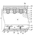
- FIG. 1 is a diagram illustrating a cross-sectional configuration of the semiconductor device according to the first embodiment of the present disclosure.
- FIG. 2 is a diagram illustrating a cross-sectional configuration of the semiconductor device according to the third embodiment of the present disclosure.
- the semiconductor device of this embodiment is formed so that one element formed on a common semiconductor substrate 1 has two functions of IGBT and FWD.
- the semiconductor substrate 1 has an N ⁇ type drift layer 2.
- a P-type base layer 3 is formed on the surface layer portion of the drift layer 2.
- a plurality of trenches 4 penetrating the base layer 3 and reaching the drift layer 2 are extended in stripes in a predetermined direction (in this embodiment, a direction perpendicular to the paper surface).
- a gate insulating film 5 made of a thermal oxide film or the like and a gate electrode 6 made of doped Poly-Si or the like are sequentially formed on the side walls of the trench 4. That is, a trench gate structure including the trench 4, the gate insulating film 5, and the gate electrode 6 is formed.
- a channel region serving as an inversion layer is formed in a portion of the base layer 3 in contact with the trench 4.
- the surface of the portion of the base layer 3 that contacts the wall surface of the trench 4 corresponds to the surface of the channel region of the present disclosure.
- an N + -type emitter layer 7 is formed on the surface layer portion of the base layer 3 so as to be in contact with the side surface of the trench 4, and a P + -type body layer 8 is formed at a position away from the side surface of the trench 4. Is formed.
- the emitter layer 7 extends in a rod shape so as to be in contact with the side surface of the trench 4 along the longitudinal direction of the trench 4, and has a structure that terminates inside the tip of the trench 4.
- the body layer 8 is sandwiched between two emitter layers 7 and extends in a rod shape along the longitudinal direction of the trench 4 (that is, the emitter layer 7), and terminates inside the tip of the trench 4.
- the emitter layer 7 and the body layer 8 have a higher impurity density than that of the base layer 3 and are structured to terminate in the base layer 3.
- the base layer 3 and the body layer 8 are configured by doping impurities such as boron, and the emitter layer 7 is configured by doping impurities such as phosphorus, arsenic, and antimony. That is, the base layer 3, the emitter layer 7 and the body layer 8 are at a level indicating 100% activation rate at the operating temperature of the semiconductor device (for example, ⁇ 40 to 150 ° C.), in other words, extrinsic. It is a level located in the region. Usually, it may not be specified to use a level indicating 100% activation rate in the semiconductor field, but this is omitted because it is common sense.
- An interlayer insulating film 9 made of BPSG or the like is formed on the base layer 3.
- a contact hole 9 a is formed in the interlayer insulating film 9, and a part of the emitter layer 7 and the body layer 8 are exposed from the interlayer insulating film 9.
- An emitter electrode 10 is formed on the interlayer insulating film 9, and the emitter electrode 10 is electrically connected to the emitter layer 7 and the body layer 8 (base layer 3) through a contact hole 9a. .
- an N-type buffer layer 11 is formed on the back side of the drift layer 2.
- the configuration of the buffer layer 11 of the present embodiment will be specifically described.
- the buffer layer 11 has a carrier density smaller than the space charge density. That is, the level activation energy in the buffer layer 11 is set larger than the thermal energy at the operating temperature at the operating temperature of the semiconductor device. In other words, the buffer layer 11 has a deep level showing an activation rate of less than 100% at the operating temperature of the semiconductor device. Furthermore, in other words, the buffer layer 11 is at a level located in the frozen region at the operating temperature of the semiconductor device.
- Such a buffer layer 11 is configured by doping at least one of impurities such as Bi, Mg, Ta, Pb, Te, Se, N, C, Ge, Sr, Cs, Ba, and S, for example. .
- the level of the buffer layer 11 in the present embodiment is a level at which a part works as a carrier. That is, the level of the buffer layer 11 is different from a so-called lifetime killer of a level located in the vicinity of MidGap formed in order to shorten the lifetime of minority carriers. It is also different from relatively deep levels such as C and Fe that compensate for majority carriers used in HFETs such as GaN.
- a P + -type collector layer 12 is selectively formed on the opposite side of the buffer layer 11 from the drift layer 2 side. That is, the side opposite to the drift layer 2 side of the buffer layer 11 is configured such that the buffer layers 11 and the collector layers 12 are alternately arranged in the cross section shown in FIG.
- a collector electrode 13 is formed on the opposite side of the buffer layer 11 to the drift layer 2 side so that the collector layer 12 and the buffer layer 11 are short-circuited.
- the N type corresponds to the first conductivity type of the present disclosure
- the P type corresponds to the second conductivity type of the present disclosure
- the emitter electrode 10 corresponds to the first electrode of the present disclosure
- the collector electrode 13 corresponds to the second electrode of the present disclosure.
- the buffer layer 11 is configured so that the carrier density is smaller than the space charge density as described above, even if the space charge density of the buffer layer 11 is increased, the carrier density of the buffer layer 11 is increased. Can be suppressed. That is, the resistance value of the buffer layer 11 can be increased. Therefore, the voltage drop when electrons flow from the buffer layer 11 to the second electrode 13 can be increased, and the IGBT can be turned on while suppressing the snapback phenomenon.
- the OFF state is a state in which neither IGBT nor FWD is ON, and a potential lower than a predetermined threshold potential is applied to the gate electrode 6 while applying a potential higher than that of the emitter electrode 10 to the collector electrode 13. Is the case.
- the operation when the FWD is turned on will be described.
- a potential lower than the threshold potential is applied to the gate electrode 6 and a potential lower than the emitter electrode 10 is applied to the collector electrode 13
- electrons are injected from the portion of the collector electrode 13 in contact with the buffer layer 11, and the emitter Holes are injected from the electrode 10 and the FWD is turned on.
- the buffer layer 11 is configured as described above and the collector layer 12 is not wide, conduction loss and current concentration can be suppressed.
- the emitter electrode 10 corresponds to the anode electrode
- the collector electrode 13 corresponds to the cathode electrode.
- the carrier density is made smaller than the space charge density of the buffer layer 11. For this reason, even if the space charge density of the buffer layer 11 is increased, the resistance value can be suppressed from decreasing. Therefore, even if the semiconductor layer having a large space charge density is used to reduce the thickness of the drift layer 2 in order to suppress the conduction loss of the IGBT and to prevent the depletion layer from reaching the collector layer 12, the buffer layer is higher than that of the conventional semiconductor device. 11 can be increased. That is, it is possible to suppress the snapback phenomenon while reducing the conduction loss of the IGBT, and it is also possible to suppress the decrease in breakdown voltage.
- the trade-off relationship among all items of the snapback phenomenon, IGBT and FWD conduction loss, current concentration, and breakdown voltage reduction can be improved at the same time.
- the semiconductor device can be manufactured only by changing the type of impurities constituting the buffer layer 11 as compared with the conventional semiconductor device in which the barrier layer is formed, and the manufacturing process is not increased. Therefore, the manufacturing cost does not increase.
- the buffer layer 11 of this embodiment is configured by two types of levels having different depths. Specifically, at the operating temperature of the semiconductor device, it is composed of a level in the freezing region and a level in the extrinsic region. The level of the extrinsic region is configured by doping with phosphorus, arsenic, antimony, or the like.
- the temperature dependence of the resistance value in the buffer layer 11 can be reduced. That is, the carrier density of the level in the frozen region varies greatly depending on the operating temperature of the semiconductor device. In other words, the resistance value of the buffer layer 11 varies greatly depending on the operating temperature of the semiconductor device. For this reason, when the buffer layer 11 is composed only of levels in the frozen region, for example, the activation rate of the lower limit temperature at the operating temperature of the semiconductor device is 1%, and the activation rate of the upper limit temperature is 10%. In such a case, the resistance value of the buffer layer 11 changes up to 10 times within the operating temperature range.
- the total activation rate is The lower limit temperature is 50.5%, and the upper limit temperature is 55%. That is, the rate of change of the resistance value of the buffer layer 11 can be reduced to 1.09 times.
- the impurity density located at the level of the frozen region is preferably changed as appropriate according to the use environment of the semiconductor device.
- FIG. 2 is a diagram illustrating a cross-sectional configuration of the semiconductor device according to the present embodiment.
- an N + -type cathode layer 14 having a carrier density larger than that of the buffer layer 11 is formed in a portion of the buffer layer 11 sandwiched between the collector layers 12.
- the collector layer 12 and the cathode layer 14 are alternately formed on the opposite side of the buffer layer 11 from the drift layer 2 side.
- the cathode layer 14 is configured by doping, for example, phosphorus, arsenic, antimony, or the like.
- the contact resistance between the buffer layer 11 (cathode layer 14) and the collector electrode 13 can be reduced. Further, since the carrier density (electrons) of the cathode layer 14 is large, it is possible to increase the electrons injected from the collector electrode 13 (cathode layer 14) during the FWD operation. Therefore, the conduction loss during the FWD operation can be further reduced.
- the first conductivity type may be P-type and the second conductivity type may be N-type.
- the buffer layer 11 is configured by being doped with at least one impurity such as Ga, In, Tl, Be, Cu, Zn, Co, and the like.
- the level of the buffer layer 11 may be formed by applying thermal or mechanical stress, or may be formed by irradiating proton beam, helium, tritium, or the like.
- the semiconductor device including the trench gate type IGBT has been described.
- a semiconductor device including the planar gate type IGBT may be used.
- the emitter layer 7 and the body layer 8 are formed on the surface layer portion of the base layer 3, and the gate insulating film is formed on the surface of the base layer 3 where the emitter layer 7 and the body layer 8 are not formed.
- a gate electrode 6 is formed via 5. Therefore, a portion of the surface of the base layer 3 where the emitter layer 7 and the body layer 8 are not formed corresponds to the surface of the base layer 3 of the present disclosure.
- the vertical semiconductor device in which a current flows in the thickness direction of the drift layer 2 has been described.
- a horizontal semiconductor device in which a current flows in the plane direction of the drift layer 2 can also be used.
- the cathode layer 14 may be formed in a region sandwiched between the collector layers 12 in the buffer layer 11 while configuring the buffer layer 11 using two different levels.
Landscapes
- Insulated Gate Type Field-Effect Transistor (AREA)
- Metal-Oxide And Bipolar Metal-Oxide Semiconductor Integrated Circuits (AREA)
- Electrodes Of Semiconductors (AREA)
Abstract
Description
/ρ2)×(L1・L2/W22)<1.6
を満たすように半導体装置を構成することが提案されている。
本開示の第1実施形態について図面を参照しつつ説明する。図1に示されるように、本実施形態の半導体装置は、共通の半導体基板1に形成された一つの素子がIGBTおよびFWDの二つの機能をもつように形成されている。
本開示の第2実施形態について説明する。本実施形態は、第1実施形態に対してバッファ層11の構成を変更したものであり、その他に関しては第1実施形態と同様であるため、ここでは説明を省略する。なお、本実施形態における半導体装置の断面構成は図1と同様である。
本開示の第3実施形態について説明する。本実施形態は、第1実施形態に対してバッファ層11にN+型のカソード層を形成したものであり、その他に関しては第1実施形態と同様であるため、ここでは説明を省略する。図2は、本実施形態における半導体装置の断面構成を示す図である。
上記各実施形態において、第1導電型をP型とし、第2導電型をN型としてもよい。この場合、バッファ層11は、例えば、Ga、In、Tl、Be、Cu、Zn、Co等の不純物の少なくとも1つがドープされて構成される。また、バッファ層11の準位は、熱的、機械的ストレスを印加することによって形成したり、陽子線、ヘリウム、トリチウム等を照射することによって形成してもよい。
Claims (6)
- 第1導電型のドリフト層(2)と、
前記ドリフト層(2)の表層部に形成された第2導電型のベース層(3)と、
前記ベース層(3)の表層部に形成された第1導電型のエミッタ層(7)と、
前記ドリフト層(2)のうち前記ベース層(3)と離間した位置に形成された第1導電型のバッファ層(11)と、
前記バッファ層(11)中に選択的に形成された第2導電型のコレクタ層(12)と、
前記ベース層(3)のうち前記ドリフト層(2)と前記エミッタ層(7)との間に挟まれた部分をチャネル領域として、当該チャネル領域に接触するゲート絶縁膜(5)と、
前記ゲート絶縁膜(5)上に形成されたゲート電極(6)と、
前記ベース層(3)および前記エミッタ層(7)と電気的に接続される第1電極(10)と、
前記バッファ層(11)および前記コレクタ層(12)と電気的に接続される第2電極(13)と、を備え、
前記バッファ層(11)は、空間電荷密度よりキャリア密度が小さくされている半導体装置。 - 前記バッファ層(11)は、凍結領域にある準位を提供する請求項1に記載の半導体装置。
- 前記バッファ層(11)は、凍結領域にある準位と、外因性領域にある準位を提供する請求項1または2に記載の半導体装置。
- 前記コレクタ層(12)は、複数のコレクタ部分(12)を含み、
前記バッファ層(11)には、前記複数のコレクタ部分(12)の間に位置する部分に、前記バッファ層(11)より浅い準位で形成され、前記バッファ層(11)よりキャリア密度が大きくされたカソード層(14)が配置されている請求項1ないし3のいずれか1つに記載の半導体装置。 - 前記第1導電型はN型であると共に前記第2導電型はP型であり、
前記バッファ層(11)は、Bi、Mg、Ta、Pb、Te、Se、N、C、Ge、Sr、Cs、Ba、Sのうちの少なくとも1つがドープされている請求項1ないし4のいずれか1つに記載の半導体装置。 - 前記第1導電型はP型であると共に前記第2導電型はN型であり、
前記バッファ層(11)は、Ga、In、Tl、Be、Cu、Zn、Coのうちの少なくとも1つがドープされている請求項1ないし4のいずれか1つに記載の半導体装置。
Priority Applications (3)
| Application Number | Priority Date | Filing Date | Title |
|---|---|---|---|
| CN201380024277.1A CN104285300A (zh) | 2012-05-07 | 2013-04-17 | 半导体装置 |
| DE201311002352 DE112013002352T5 (de) | 2012-05-07 | 2013-04-17 | Halbleitervorrichtung |
| US14/391,197 US20150115316A1 (en) | 2012-05-07 | 2013-04-17 | Semiconductor device |
Applications Claiming Priority (2)
| Application Number | Priority Date | Filing Date | Title |
|---|---|---|---|
| JP2012-106013 | 2012-05-07 | ||
| JP2012106013A JP2013235891A (ja) | 2012-05-07 | 2012-05-07 | 半導体装置 |
Publications (1)
| Publication Number | Publication Date |
|---|---|
| WO2013168366A1 true WO2013168366A1 (ja) | 2013-11-14 |
Family
ID=49550435
Family Applications (1)
| Application Number | Title | Priority Date | Filing Date |
|---|---|---|---|
| PCT/JP2013/002598 Ceased WO2013168366A1 (ja) | 2012-05-07 | 2013-04-17 | 半導体装置 |
Country Status (5)
| Country | Link |
|---|---|
| US (1) | US20150115316A1 (ja) |
| JP (1) | JP2013235891A (ja) |
| CN (1) | CN104285300A (ja) |
| DE (1) | DE112013002352T5 (ja) |
| WO (1) | WO2013168366A1 (ja) |
Cited By (2)
| Publication number | Priority date | Publication date | Assignee | Title |
|---|---|---|---|---|
| CN103594467A (zh) * | 2013-11-27 | 2014-02-19 | 杭州士兰集成电路有限公司 | 集成续流二极管的功率半导体器件及其形成方法 |
| US9391071B2 (en) | 2014-09-12 | 2016-07-12 | Kabushiki Kaisha Toshiba | Semiconductor device |
Families Citing this family (16)
| Publication number | Priority date | Publication date | Assignee | Title |
|---|---|---|---|---|
| US9419080B2 (en) | 2013-12-11 | 2016-08-16 | Infineon Technologies Ag | Semiconductor device with recombination region |
| US9543389B2 (en) * | 2013-12-11 | 2017-01-10 | Infineon Technologies Ag | Semiconductor device with recombination region |
| US9159819B2 (en) * | 2014-02-20 | 2015-10-13 | Infineon Technologies Ag | Semiconductor device and RC-IGBT with zones directly adjoining a rear side electrode |
| JP6582762B2 (ja) | 2015-09-03 | 2019-10-02 | 株式会社デンソー | 半導体装置 |
| CN105244273B (zh) * | 2015-11-04 | 2018-10-26 | 株洲南车时代电气股份有限公司 | 一种逆导igbt的制备方法 |
| JP2017208413A (ja) | 2016-05-17 | 2017-11-24 | 株式会社デンソー | 半導体装置 |
| CN106206679B (zh) * | 2016-08-31 | 2019-08-23 | 电子科技大学 | 一种逆导型igbt |
| JP6881463B2 (ja) * | 2016-09-14 | 2021-06-02 | 富士電機株式会社 | Rc−igbtおよびその製造方法 |
| JP6935731B2 (ja) | 2017-11-16 | 2021-09-15 | 株式会社デンソー | 半導体装置 |
| EP3598505B1 (en) * | 2018-07-19 | 2023-02-15 | Mitsubishi Electric R&D Centre Europe B.V. | Temperature estimation of a power semiconductor device |
| JP7010184B2 (ja) * | 2018-09-13 | 2022-01-26 | 株式会社デンソー | 半導体装置 |
| CN110676314B (zh) | 2019-10-23 | 2021-05-04 | 广东美的白色家电技术创新中心有限公司 | 一种绝缘栅双极型晶体管、功率模块及生活电器 |
| JP7352437B2 (ja) * | 2019-10-25 | 2023-09-28 | 株式会社東芝 | 半導体装置 |
| CN113809147A (zh) | 2020-06-17 | 2021-12-17 | 富士电机株式会社 | 半导体装置以及半导体装置的制造方法 |
| JP7718052B2 (ja) * | 2020-06-17 | 2025-08-05 | 富士電機株式会社 | 半導体装置および半導体装置の製造方法 |
| US12538536B2 (en) | 2020-11-06 | 2026-01-27 | Hitachi Energy Ltd | Power semiconductor device and operating method |
Citations (4)
| Publication number | Priority date | Publication date | Assignee | Title |
|---|---|---|---|---|
| JP2000101066A (ja) * | 1998-09-25 | 2000-04-07 | Toshiba Corp | 電力用半導体素子 |
| JP2003303965A (ja) * | 2002-04-09 | 2003-10-24 | Toshiba Corp | 半導体素子及びその製造方法 |
| JP2007288158A (ja) * | 2006-03-22 | 2007-11-01 | Denso Corp | 半導体装置およびその設計方法 |
| US20080054369A1 (en) * | 2006-08-31 | 2008-03-06 | Infineon Technologies | Semiconductor device with a field stop zone and process of producing the same |
Family Cites Families (8)
| Publication number | Priority date | Publication date | Assignee | Title |
|---|---|---|---|---|
| JPH03194974A (ja) * | 1989-12-22 | 1991-08-26 | Fuji Electric Co Ltd | Mos型半導体装置 |
| KR100275756B1 (ko) * | 1998-08-27 | 2000-12-15 | 김덕중 | 트렌치 절연 게이트 바이폴라 트랜지스터 |
| DE10055446B4 (de) * | 1999-11-26 | 2012-08-23 | Fuji Electric Co., Ltd. | Halbleiterbauelement und Verfahren zu seiner Herstellung |
| US6815767B2 (en) * | 2001-02-01 | 2004-11-09 | Mitsubishi Denki Kabushiki Kaisha | Insulated gate transistor |
| US8866150B2 (en) * | 2007-05-31 | 2014-10-21 | Cree, Inc. | Silicon carbide power devices including P-type epitaxial layers and direct ohmic contacts |
| JP5365009B2 (ja) * | 2008-01-23 | 2013-12-11 | 富士電機株式会社 | 半導体装置およびその製造方法 |
| JP4929304B2 (ja) * | 2009-03-13 | 2012-05-09 | 株式会社東芝 | 半導体装置 |
| JP5216801B2 (ja) * | 2010-03-24 | 2013-06-19 | 株式会社東芝 | 半導体装置 |
-
2012
- 2012-05-07 JP JP2012106013A patent/JP2013235891A/ja active Pending
-
2013
- 2013-04-17 DE DE201311002352 patent/DE112013002352T5/de not_active Withdrawn
- 2013-04-17 CN CN201380024277.1A patent/CN104285300A/zh active Pending
- 2013-04-17 WO PCT/JP2013/002598 patent/WO2013168366A1/ja not_active Ceased
- 2013-04-17 US US14/391,197 patent/US20150115316A1/en not_active Abandoned
Patent Citations (4)
| Publication number | Priority date | Publication date | Assignee | Title |
|---|---|---|---|---|
| JP2000101066A (ja) * | 1998-09-25 | 2000-04-07 | Toshiba Corp | 電力用半導体素子 |
| JP2003303965A (ja) * | 2002-04-09 | 2003-10-24 | Toshiba Corp | 半導体素子及びその製造方法 |
| JP2007288158A (ja) * | 2006-03-22 | 2007-11-01 | Denso Corp | 半導体装置およびその設計方法 |
| US20080054369A1 (en) * | 2006-08-31 | 2008-03-06 | Infineon Technologies | Semiconductor device with a field stop zone and process of producing the same |
Non-Patent Citations (1)
| Title |
|---|
| S. VOSS ET AL.: "Optimization of the temperature dependence of the anode-side current gain of IGBTs by field-stop design", PROCEEDINGS OF THE 22ND INTERNATIONAL SYMPOSIUM ON POWER SEMICONDUCTOR DEVICES & ICS, 6 June 2010 (2010-06-06), HIROSHIMA, pages 141 - 144 * |
Cited By (2)
| Publication number | Priority date | Publication date | Assignee | Title |
|---|---|---|---|---|
| CN103594467A (zh) * | 2013-11-27 | 2014-02-19 | 杭州士兰集成电路有限公司 | 集成续流二极管的功率半导体器件及其形成方法 |
| US9391071B2 (en) | 2014-09-12 | 2016-07-12 | Kabushiki Kaisha Toshiba | Semiconductor device |
Also Published As
| Publication number | Publication date |
|---|---|
| CN104285300A (zh) | 2015-01-14 |
| JP2013235891A (ja) | 2013-11-21 |
| US20150115316A1 (en) | 2015-04-30 |
| DE112013002352T5 (de) | 2015-01-22 |
Similar Documents
| Publication | Publication Date | Title |
|---|---|---|
| WO2013168366A1 (ja) | 半導体装置 | |
| CN109964317B (zh) | 半导体装置 | |
| CN104871312B (zh) | 半导体装置 | |
| JP6063915B2 (ja) | 逆導通igbt | |
| JP6053050B2 (ja) | 逆導通igbt | |
| JPWO2018220879A1 (ja) | 半導体装置 | |
| US10418470B2 (en) | Semiconductor device having IGBT portion and diode portion | |
| JP2019169597A (ja) | 半導体装置 | |
| US20130248882A1 (en) | Semiconductor device | |
| CN105706238A (zh) | 半导体装置 | |
| JP2007184486A (ja) | 半導体装置 | |
| JP2009026797A (ja) | 半導体装置 | |
| WO2013046578A1 (ja) | 半導体装置 | |
| WO2013065247A1 (ja) | 半導体装置 | |
| US20190081030A1 (en) | Semiconductor device | |
| TW201635528A (zh) | 半導體裝置 | |
| JP2017079234A (ja) | 半導体装置 | |
| WO2013168367A1 (ja) | 半導体装置 | |
| JP2012069735A (ja) | 半導体装置 | |
| WO2021182352A1 (ja) | 半導体装置 | |
| JP2008244466A (ja) | 半導体装置 | |
| US11289476B2 (en) | Semiconductor device including carrier injection layers | |
| US11004964B2 (en) | Semiconductor device | |
| US20150187919A1 (en) | Power semiconductor device | |
| JP6266480B2 (ja) | 半導体装置 |
Legal Events
| Date | Code | Title | Description |
|---|---|---|---|
| 121 | Ep: the epo has been informed by wipo that ep was designated in this application |
Ref document number: 13788085 Country of ref document: EP Kind code of ref document: A1 |
|
| WWE | Wipo information: entry into national phase |
Ref document number: 14391197 Country of ref document: US |
|
| WWE | Wipo information: entry into national phase |
Ref document number: 112013002352 Country of ref document: DE Ref document number: 1120130023520 Country of ref document: DE |
|
| 122 | Ep: pct application non-entry in european phase |
Ref document number: 13788085 Country of ref document: EP Kind code of ref document: A1 |