WO2013168237A1 - 半導体接合保護用ガラス組成物、半導体装置の製造方法及び半導体装置 - Google Patents
半導体接合保護用ガラス組成物、半導体装置の製造方法及び半導体装置 Download PDFInfo
- Publication number
- WO2013168237A1 WO2013168237A1 PCT/JP2012/061777 JP2012061777W WO2013168237A1 WO 2013168237 A1 WO2013168237 A1 WO 2013168237A1 JP 2012061777 W JP2012061777 W JP 2012061777W WO 2013168237 A1 WO2013168237 A1 WO 2013168237A1
- Authority
- WO
- WIPO (PCT)
- Prior art keywords
- mol
- junction
- semiconductor
- content
- range
- Prior art date
Links
- 239000004065 semiconductor Substances 0.000 title claims abstract description 379
- 239000011521 glass Substances 0.000 title claims abstract description 288
- 239000000203 mixture Substances 0.000 title claims abstract description 161
- 238000004519 manufacturing process Methods 0.000 title claims abstract description 95
- 238000000034 method Methods 0.000 title description 81
- XLOMVQKBTHCTTD-UHFFFAOYSA-N zinc oxide Inorganic materials [Zn]=O XLOMVQKBTHCTTD-UHFFFAOYSA-N 0.000 claims abstract description 42
- 229910000287 alkaline earth metal oxide Inorganic materials 0.000 claims abstract description 26
- 229910052785 arsenic Inorganic materials 0.000 claims abstract description 24
- 229910052787 antimony Inorganic materials 0.000 claims abstract description 20
- 229910052744 lithium Inorganic materials 0.000 claims abstract description 20
- 229910052700 potassium Inorganic materials 0.000 claims abstract description 20
- 229910052708 sodium Inorganic materials 0.000 claims abstract description 20
- 229910052745 lead Inorganic materials 0.000 claims abstract description 19
- 239000000758 substrate Substances 0.000 claims description 96
- 229910004298 SiO 2 Inorganic materials 0.000 claims description 52
- 229910018072 Al 2 O 3 Inorganic materials 0.000 claims description 40
- 229910052784 alkaline earth metal Inorganic materials 0.000 claims description 20
- 150000001342 alkaline earth metals Chemical class 0.000 claims description 20
- 229910000480 nickel oxide Inorganic materials 0.000 claims description 20
- GNRSAWUEBMWBQH-UHFFFAOYSA-N oxonickel Chemical compound [Ni]=O GNRSAWUEBMWBQH-UHFFFAOYSA-N 0.000 claims description 20
- -1 B 2 O 3 Inorganic materials 0.000 claims description 17
- AMWRITDGCCNYAT-UHFFFAOYSA-L hydroxy(oxo)manganese;manganese Chemical compound [Mn].O[Mn]=O.O[Mn]=O AMWRITDGCCNYAT-UHFFFAOYSA-L 0.000 claims description 12
- QPLDLSVMHZLSFG-UHFFFAOYSA-N Copper oxide Chemical compound [Cu]=O QPLDLSVMHZLSFG-UHFFFAOYSA-N 0.000 claims description 6
- 239000005751 Copper oxide Substances 0.000 claims description 6
- 229910000431 copper oxide Inorganic materials 0.000 claims description 6
- 229910044991 metal oxide Inorganic materials 0.000 claims description 6
- 150000004706 metal oxides Chemical class 0.000 claims description 6
- RVTZCBVAJQQJTK-UHFFFAOYSA-N oxygen(2-);zirconium(4+) Chemical compound [O-2].[O-2].[Zr+4] RVTZCBVAJQQJTK-UHFFFAOYSA-N 0.000 claims description 6
- 229910001928 zirconium oxide Inorganic materials 0.000 claims description 6
- 230000001681 protective effect Effects 0.000 claims description 4
- QVQLCTNNEUAWMS-UHFFFAOYSA-N barium oxide Inorganic materials [Ba]=O QVQLCTNNEUAWMS-UHFFFAOYSA-N 0.000 claims 1
- ODINCKMPIJJUCX-UHFFFAOYSA-N calcium oxide Inorganic materials [Ca]=O ODINCKMPIJJUCX-UHFFFAOYSA-N 0.000 claims 1
- CPLXHLVBOLITMK-UHFFFAOYSA-N magnesium oxide Inorganic materials [Mg]=O CPLXHLVBOLITMK-UHFFFAOYSA-N 0.000 claims 1
- 239000000463 material Substances 0.000 abstract description 25
- BPQQTUXANYXVAA-UHFFFAOYSA-N Orthosilicate Chemical compound [O-][Si]([O-])([O-])[O-] BPQQTUXANYXVAA-UHFFFAOYSA-N 0.000 abstract description 11
- VYPSYNLAJGMNEJ-UHFFFAOYSA-N Silicium dioxide Chemical compound O=[Si]=O VYPSYNLAJGMNEJ-UHFFFAOYSA-N 0.000 abstract description 4
- 229910011255 B2O3 Inorganic materials 0.000 abstract 1
- PNEYBMLMFCGWSK-UHFFFAOYSA-N aluminium oxide Inorganic materials [O-2].[O-2].[O-2].[Al+3].[Al+3] PNEYBMLMFCGWSK-UHFFFAOYSA-N 0.000 abstract 1
- 229910052681 coesite Inorganic materials 0.000 abstract 1
- 229910052593 corundum Inorganic materials 0.000 abstract 1
- 229910052906 cristobalite Inorganic materials 0.000 abstract 1
- 239000000377 silicon dioxide Substances 0.000 abstract 1
- 229910052682 stishovite Inorganic materials 0.000 abstract 1
- 229910052905 tridymite Inorganic materials 0.000 abstract 1
- 229910001845 yogo sapphire Inorganic materials 0.000 abstract 1
- 238000011156 evaluation Methods 0.000 description 43
- 238000009792 diffusion process Methods 0.000 description 38
- XUIMIQQOPSSXEZ-UHFFFAOYSA-N Silicon Chemical compound [Si] XUIMIQQOPSSXEZ-UHFFFAOYSA-N 0.000 description 27
- 229910052710 silicon Inorganic materials 0.000 description 27
- 239000010703 silicon Substances 0.000 description 27
- 230000015572 biosynthetic process Effects 0.000 description 25
- 238000010304 firing Methods 0.000 description 17
- 239000012535 impurity Substances 0.000 description 13
- 239000002994 raw material Substances 0.000 description 13
- 238000005520 cutting process Methods 0.000 description 12
- 238000004017 vitrification Methods 0.000 description 12
- 229920002120 photoresistant polymer Polymers 0.000 description 11
- 239000000126 substance Substances 0.000 description 11
- 230000000052 comparative effect Effects 0.000 description 10
- 238000002425 crystallisation Methods 0.000 description 10
- 230000008025 crystallization Effects 0.000 description 10
- 238000010586 diagram Methods 0.000 description 10
- 238000002161 passivation Methods 0.000 description 9
- 238000001962 electrophoresis Methods 0.000 description 8
- 238000009413 insulation Methods 0.000 description 8
- 238000007747 plating Methods 0.000 description 8
- BASFCYQUMIYNBI-UHFFFAOYSA-N platinum Chemical compound [Pt] BASFCYQUMIYNBI-UHFFFAOYSA-N 0.000 description 8
- 230000015556 catabolic process Effects 0.000 description 7
- 238000002474 experimental method Methods 0.000 description 6
- PXHVJJICTQNCMI-UHFFFAOYSA-N nickel Substances [Ni] PXHVJJICTQNCMI-UHFFFAOYSA-N 0.000 description 6
- 238000002360 preparation method Methods 0.000 description 6
- 229910052796 boron Inorganic materials 0.000 description 5
- 239000000155 melt Substances 0.000 description 5
- 230000003647 oxidation Effects 0.000 description 5
- 238000007254 oxidation reaction Methods 0.000 description 5
- 238000007796 conventional method Methods 0.000 description 4
- 238000005530 etching Methods 0.000 description 4
- 238000005304 joining Methods 0.000 description 4
- 238000005259 measurement Methods 0.000 description 4
- 150000004767 nitrides Chemical class 0.000 description 4
- 239000002245 particle Substances 0.000 description 4
- 229910052697 platinum Inorganic materials 0.000 description 4
- 238000001259 photo etching Methods 0.000 description 3
- 238000007788 roughening Methods 0.000 description 3
- MYMOFIZGZYHOMD-UHFFFAOYSA-N Dioxygen Chemical compound O=O MYMOFIZGZYHOMD-UHFFFAOYSA-N 0.000 description 2
- QZPSXPBJTPJTSZ-UHFFFAOYSA-N aqua regia Chemical compound Cl.O[N+]([O-])=O QZPSXPBJTPJTSZ-UHFFFAOYSA-N 0.000 description 2
- QVGXLLKOCUKJST-UHFFFAOYSA-N atomic oxygen Chemical compound [O] QVGXLLKOCUKJST-UHFFFAOYSA-N 0.000 description 2
- 229910001882 dioxygen Inorganic materials 0.000 description 2
- 230000000694 effects Effects 0.000 description 2
- 230000007613 environmental effect Effects 0.000 description 2
- 238000005468 ion implantation Methods 0.000 description 2
- 229910052760 oxygen Inorganic materials 0.000 description 2
- 239000001301 oxygen Substances 0.000 description 2
- 239000011347 resin Substances 0.000 description 2
- 229920005989 resin Polymers 0.000 description 2
- 229910052814 silicon oxide Inorganic materials 0.000 description 2
- 238000003756 stirring Methods 0.000 description 2
- 239000013078 crystal Substances 0.000 description 1
- 238000007572 expansion measurement Methods 0.000 description 1
- 238000005187 foaming Methods 0.000 description 1
- 230000009477 glass transition Effects 0.000 description 1
- 238000012986 modification Methods 0.000 description 1
- 230000004048 modification Effects 0.000 description 1
- 239000000075 oxide glass Substances 0.000 description 1
- 229910052698 phosphorus Inorganic materials 0.000 description 1
- 238000004528 spin coating Methods 0.000 description 1
- 238000003892 spreading Methods 0.000 description 1
- 230000000930 thermomechanical effect Effects 0.000 description 1
- 231100000331 toxic Toxicity 0.000 description 1
- 230000002588 toxic effect Effects 0.000 description 1
Images


Classifications
-
- H—ELECTRICITY
- H01—ELECTRIC ELEMENTS
- H01L—SEMICONDUCTOR DEVICES NOT COVERED BY CLASS H10
- H01L23/00—Details of semiconductor or other solid state devices
- H01L23/28—Encapsulations, e.g. encapsulating layers, coatings, e.g. for protection
- H01L23/29—Encapsulations, e.g. encapsulating layers, coatings, e.g. for protection characterised by the material, e.g. carbon
- H01L23/291—Oxides or nitrides or carbides, e.g. ceramics, glass
-
- C—CHEMISTRY; METALLURGY
- C03—GLASS; MINERAL OR SLAG WOOL
- C03C—CHEMICAL COMPOSITION OF GLASSES, GLAZES OR VITREOUS ENAMELS; SURFACE TREATMENT OF GLASS; SURFACE TREATMENT OF FIBRES OR FILAMENTS MADE FROM GLASS, MINERALS OR SLAGS; JOINING GLASS TO GLASS OR OTHER MATERIALS
- C03C3/00—Glass compositions
- C03C3/04—Glass compositions containing silica
- C03C3/076—Glass compositions containing silica with 40% to 90% silica, by weight
- C03C3/089—Glass compositions containing silica with 40% to 90% silica, by weight containing boron
- C03C3/091—Glass compositions containing silica with 40% to 90% silica, by weight containing boron containing aluminium
- C03C3/093—Glass compositions containing silica with 40% to 90% silica, by weight containing boron containing aluminium containing zinc or zirconium
-
- C—CHEMISTRY; METALLURGY
- C03—GLASS; MINERAL OR SLAG WOOL
- C03C—CHEMICAL COMPOSITION OF GLASSES, GLAZES OR VITREOUS ENAMELS; SURFACE TREATMENT OF GLASS; SURFACE TREATMENT OF FIBRES OR FILAMENTS MADE FROM GLASS, MINERALS OR SLAGS; JOINING GLASS TO GLASS OR OTHER MATERIALS
- C03C8/00—Enamels; Glazes; Fusion seal compositions being frit compositions having non-frit additions
- C03C8/02—Frit compositions, i.e. in a powdered or comminuted form
- C03C8/04—Frit compositions, i.e. in a powdered or comminuted form containing zinc
-
- C—CHEMISTRY; METALLURGY
- C03—GLASS; MINERAL OR SLAG WOOL
- C03C—CHEMICAL COMPOSITION OF GLASSES, GLAZES OR VITREOUS ENAMELS; SURFACE TREATMENT OF GLASS; SURFACE TREATMENT OF FIBRES OR FILAMENTS MADE FROM GLASS, MINERALS OR SLAGS; JOINING GLASS TO GLASS OR OTHER MATERIALS
- C03C8/00—Enamels; Glazes; Fusion seal compositions being frit compositions having non-frit additions
- C03C8/24—Fusion seal compositions being frit compositions having non-frit additions, i.e. for use as seals between dissimilar materials, e.g. glass and metal; Glass solders
-
- H—ELECTRICITY
- H01—ELECTRIC ELEMENTS
- H01L—SEMICONDUCTOR DEVICES NOT COVERED BY CLASS H10
- H01L21/00—Processes or apparatus adapted for the manufacture or treatment of semiconductor or solid state devices or of parts thereof
- H01L21/02—Manufacture or treatment of semiconductor devices or of parts thereof
- H01L21/02104—Forming layers
- H01L21/02107—Forming insulating materials on a substrate
- H01L21/02109—Forming insulating materials on a substrate characterised by the type of layer, e.g. type of material, porous/non-porous, pre-cursors, mixtures or laminates
- H01L21/02112—Forming insulating materials on a substrate characterised by the type of layer, e.g. type of material, porous/non-porous, pre-cursors, mixtures or laminates characterised by the material of the layer
- H01L21/02123—Forming insulating materials on a substrate characterised by the type of layer, e.g. type of material, porous/non-porous, pre-cursors, mixtures or laminates characterised by the material of the layer the material containing silicon
- H01L21/02164—Forming insulating materials on a substrate characterised by the type of layer, e.g. type of material, porous/non-porous, pre-cursors, mixtures or laminates characterised by the material of the layer the material containing silicon the material being a silicon oxide, e.g. SiO2
-
- H—ELECTRICITY
- H01—ELECTRIC ELEMENTS
- H01L—SEMICONDUCTOR DEVICES NOT COVERED BY CLASS H10
- H01L21/00—Processes or apparatus adapted for the manufacture or treatment of semiconductor or solid state devices or of parts thereof
- H01L21/02—Manufacture or treatment of semiconductor devices or of parts thereof
- H01L21/02104—Forming layers
- H01L21/02107—Forming insulating materials on a substrate
- H01L21/02109—Forming insulating materials on a substrate characterised by the type of layer, e.g. type of material, porous/non-porous, pre-cursors, mixtures or laminates
- H01L21/02112—Forming insulating materials on a substrate characterised by the type of layer, e.g. type of material, porous/non-porous, pre-cursors, mixtures or laminates characterised by the material of the layer
- H01L21/02172—Forming insulating materials on a substrate characterised by the type of layer, e.g. type of material, porous/non-porous, pre-cursors, mixtures or laminates characterised by the material of the layer the material containing at least one metal element, e.g. metal oxides, metal nitrides, metal oxynitrides or metal carbides
- H01L21/02175—Forming insulating materials on a substrate characterised by the type of layer, e.g. type of material, porous/non-porous, pre-cursors, mixtures or laminates characterised by the material of the layer the material containing at least one metal element, e.g. metal oxides, metal nitrides, metal oxynitrides or metal carbides characterised by the metal
- H01L21/02178—Forming insulating materials on a substrate characterised by the type of layer, e.g. type of material, porous/non-porous, pre-cursors, mixtures or laminates characterised by the material of the layer the material containing at least one metal element, e.g. metal oxides, metal nitrides, metal oxynitrides or metal carbides characterised by the metal the material containing aluminium, e.g. Al2O3
-
- H—ELECTRICITY
- H01—ELECTRIC ELEMENTS
- H01L—SEMICONDUCTOR DEVICES NOT COVERED BY CLASS H10
- H01L21/00—Processes or apparatus adapted for the manufacture or treatment of semiconductor or solid state devices or of parts thereof
- H01L21/02—Manufacture or treatment of semiconductor devices or of parts thereof
- H01L21/02104—Forming layers
- H01L21/02107—Forming insulating materials on a substrate
- H01L21/02109—Forming insulating materials on a substrate characterised by the type of layer, e.g. type of material, porous/non-porous, pre-cursors, mixtures or laminates
- H01L21/02112—Forming insulating materials on a substrate characterised by the type of layer, e.g. type of material, porous/non-porous, pre-cursors, mixtures or laminates characterised by the material of the layer
- H01L21/02172—Forming insulating materials on a substrate characterised by the type of layer, e.g. type of material, porous/non-porous, pre-cursors, mixtures or laminates characterised by the material of the layer the material containing at least one metal element, e.g. metal oxides, metal nitrides, metal oxynitrides or metal carbides
- H01L21/02175—Forming insulating materials on a substrate characterised by the type of layer, e.g. type of material, porous/non-porous, pre-cursors, mixtures or laminates characterised by the material of the layer the material containing at least one metal element, e.g. metal oxides, metal nitrides, metal oxynitrides or metal carbides characterised by the metal
- H01L21/02192—Forming insulating materials on a substrate characterised by the type of layer, e.g. type of material, porous/non-porous, pre-cursors, mixtures or laminates characterised by the material of the layer the material containing at least one metal element, e.g. metal oxides, metal nitrides, metal oxynitrides or metal carbides characterised by the metal the material containing at least one rare earth metal element, e.g. oxides of lanthanides, scandium or yttrium
-
- H—ELECTRICITY
- H01—ELECTRIC ELEMENTS
- H01L—SEMICONDUCTOR DEVICES NOT COVERED BY CLASS H10
- H01L21/00—Processes or apparatus adapted for the manufacture or treatment of semiconductor or solid state devices or of parts thereof
- H01L21/02—Manufacture or treatment of semiconductor devices or of parts thereof
- H01L21/02104—Forming layers
- H01L21/02107—Forming insulating materials on a substrate
- H01L21/02296—Forming insulating materials on a substrate characterised by the treatment performed before or after the formation of the layer
- H01L21/02318—Forming insulating materials on a substrate characterised by the treatment performed before or after the formation of the layer post-treatment
- H01L21/02345—Forming insulating materials on a substrate characterised by the treatment performed before or after the formation of the layer post-treatment treatment by exposure to radiation, e.g. visible light
-
- H—ELECTRICITY
- H01—ELECTRIC ELEMENTS
- H01L—SEMICONDUCTOR DEVICES NOT COVERED BY CLASS H10
- H01L21/00—Processes or apparatus adapted for the manufacture or treatment of semiconductor or solid state devices or of parts thereof
- H01L21/02—Manufacture or treatment of semiconductor devices or of parts thereof
- H01L21/04—Manufacture or treatment of semiconductor devices or of parts thereof the devices having potential barriers, e.g. a PN junction, depletion layer or carrier concentration layer
- H01L21/50—Assembly of semiconductor devices using processes or apparatus not provided for in a single one of the subgroups H01L21/06 - H01L21/326, e.g. sealing of a cap to a base of a container
- H01L21/56—Encapsulations, e.g. encapsulation layers, coatings
-
- H—ELECTRICITY
- H01—ELECTRIC ELEMENTS
- H01L—SEMICONDUCTOR DEVICES NOT COVERED BY CLASS H10
- H01L21/00—Processes or apparatus adapted for the manufacture or treatment of semiconductor or solid state devices or of parts thereof
- H01L21/70—Manufacture or treatment of devices consisting of a plurality of solid state components formed in or on a common substrate or of parts thereof; Manufacture of integrated circuit devices or of parts thereof
- H01L21/71—Manufacture of specific parts of devices defined in group H01L21/70
- H01L21/76—Making of isolation regions between components
- H01L21/761—PN junctions
-
- H—ELECTRICITY
- H01—ELECTRIC ELEMENTS
- H01L—SEMICONDUCTOR DEVICES NOT COVERED BY CLASS H10
- H01L21/00—Processes or apparatus adapted for the manufacture or treatment of semiconductor or solid state devices or of parts thereof
- H01L21/70—Manufacture or treatment of devices consisting of a plurality of solid state components formed in or on a common substrate or of parts thereof; Manufacture of integrated circuit devices or of parts thereof
- H01L21/71—Manufacture of specific parts of devices defined in group H01L21/70
- H01L21/76—Making of isolation regions between components
- H01L21/762—Dielectric regions, e.g. EPIC dielectric isolation, LOCOS; Trench refilling techniques, SOI technology, use of channel stoppers
- H01L21/76224—Dielectric regions, e.g. EPIC dielectric isolation, LOCOS; Trench refilling techniques, SOI technology, use of channel stoppers using trench refilling with dielectric materials
- H01L21/76232—Dielectric regions, e.g. EPIC dielectric isolation, LOCOS; Trench refilling techniques, SOI technology, use of channel stoppers using trench refilling with dielectric materials of trenches having a shape other than rectangular or V-shape, e.g. rounded corners, oblique or rounded trench walls
-
- H—ELECTRICITY
- H01—ELECTRIC ELEMENTS
- H01L—SEMICONDUCTOR DEVICES NOT COVERED BY CLASS H10
- H01L23/00—Details of semiconductor or other solid state devices
- H01L23/28—Encapsulations, e.g. encapsulating layers, coatings, e.g. for protection
- H01L23/31—Encapsulations, e.g. encapsulating layers, coatings, e.g. for protection characterised by the arrangement or shape
- H01L23/3157—Partial encapsulation or coating
- H01L23/3171—Partial encapsulation or coating the coating being directly applied to the semiconductor body, e.g. passivation layer
-
- H—ELECTRICITY
- H01—ELECTRIC ELEMENTS
- H01L—SEMICONDUCTOR DEVICES NOT COVERED BY CLASS H10
- H01L23/00—Details of semiconductor or other solid state devices
- H01L23/28—Encapsulations, e.g. encapsulating layers, coatings, e.g. for protection
- H01L23/31—Encapsulations, e.g. encapsulating layers, coatings, e.g. for protection characterised by the arrangement or shape
- H01L23/3157—Partial encapsulation or coating
- H01L23/3185—Partial encapsulation or coating the coating covering also the sidewalls of the semiconductor body
-
- H—ELECTRICITY
- H01—ELECTRIC ELEMENTS
- H01L—SEMICONDUCTOR DEVICES NOT COVERED BY CLASS H10
- H01L29/00—Semiconductor devices specially adapted for rectifying, amplifying, oscillating or switching and having potential barriers; Capacitors or resistors having potential barriers, e.g. a PN-junction depletion layer or carrier concentration layer; Details of semiconductor bodies or of electrodes thereof ; Multistep manufacturing processes therefor
- H01L29/66—Types of semiconductor device ; Multistep manufacturing processes therefor
- H01L29/66007—Multistep manufacturing processes
- H01L29/66075—Multistep manufacturing processes of devices having semiconductor bodies comprising group 14 or group 13/15 materials
- H01L29/66083—Multistep manufacturing processes of devices having semiconductor bodies comprising group 14 or group 13/15 materials the devices being controllable only by variation of the electric current supplied or the electric potential applied, to one or more of the electrodes carrying the current to be rectified, amplified, oscillated or switched, e.g. two-terminal devices
- H01L29/6609—Diodes
- H01L29/66136—PN junction diodes
-
- H—ELECTRICITY
- H01—ELECTRIC ELEMENTS
- H01L—SEMICONDUCTOR DEVICES NOT COVERED BY CLASS H10
- H01L29/00—Semiconductor devices specially adapted for rectifying, amplifying, oscillating or switching and having potential barriers; Capacitors or resistors having potential barriers, e.g. a PN-junction depletion layer or carrier concentration layer; Details of semiconductor bodies or of electrodes thereof ; Multistep manufacturing processes therefor
- H01L29/66—Types of semiconductor device ; Multistep manufacturing processes therefor
- H01L29/86—Types of semiconductor device ; Multistep manufacturing processes therefor controllable only by variation of the electric current supplied, or only the electric potential applied, to one or more of the electrodes carrying the current to be rectified, amplified, oscillated or switched
- H01L29/861—Diodes
- H01L29/8611—Planar PN junction diodes
-
- H—ELECTRICITY
- H01—ELECTRIC ELEMENTS
- H01L—SEMICONDUCTOR DEVICES NOT COVERED BY CLASS H10
- H01L29/00—Semiconductor devices specially adapted for rectifying, amplifying, oscillating or switching and having potential barriers; Capacitors or resistors having potential barriers, e.g. a PN-junction depletion layer or carrier concentration layer; Details of semiconductor bodies or of electrodes thereof ; Multistep manufacturing processes therefor
- H01L29/66—Types of semiconductor device ; Multistep manufacturing processes therefor
- H01L29/86—Types of semiconductor device ; Multistep manufacturing processes therefor controllable only by variation of the electric current supplied, or only the electric potential applied, to one or more of the electrodes carrying the current to be rectified, amplified, oscillated or switched
- H01L29/861—Diodes
- H01L29/8613—Mesa PN junction diodes
-
- C—CHEMISTRY; METALLURGY
- C03—GLASS; MINERAL OR SLAG WOOL
- C03C—CHEMICAL COMPOSITION OF GLASSES, GLAZES OR VITREOUS ENAMELS; SURFACE TREATMENT OF GLASS; SURFACE TREATMENT OF FIBRES OR FILAMENTS MADE FROM GLASS, MINERALS OR SLAGS; JOINING GLASS TO GLASS OR OTHER MATERIALS
- C03C2207/00—Compositions specially applicable for the manufacture of vitreous enamels
-
- H—ELECTRICITY
- H01—ELECTRIC ELEMENTS
- H01L—SEMICONDUCTOR DEVICES NOT COVERED BY CLASS H10
- H01L2924/00—Indexing scheme for arrangements or methods for connecting or disconnecting semiconductor or solid-state bodies as covered by H01L24/00
- H01L2924/0001—Technical content checked by a classifier
- H01L2924/0002—Not covered by any one of groups H01L24/00, H01L24/00 and H01L2224/00
Definitions
- the present invention relates to a glass composition for protecting a semiconductor junction, a method for manufacturing a semiconductor device, and a semiconductor device.
- a semiconductor device manufacturing method is known in which a passivation glass layer is formed so as to cover a pn junction exposed portion in the process of manufacturing a mesa type semiconductor device (see, for example, Patent Document 1).
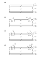
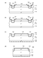
- FIGS. 14 and 15 are views for explaining such a conventional method of manufacturing a semiconductor device.
- 14 (a) to 14 (d) and FIGS. 15 (a) to 15 (d) are process diagrams.
- the conventional semiconductor device manufacturing method includes a “semiconductor substrate forming step”, “groove forming step”, “glass layer forming step”, “photoresist forming step”, and “oxide removal”. Step, “roughened region forming step”, “electrode forming step” and “semiconductor substrate cutting step” are included in this order.
- a conventional method for manufacturing a semiconductor device will be described in the order of steps.
- n + -type diffusion layer 912 is diffused from one surface of n ⁇ -type semiconductor substrate (n ⁇ -type silicon substrate) 910, and n-type impurities from the other surface are diffused.
- An n + -type diffusion layer 914 is formed by diffusion to form a semiconductor substrate in which a pn junction parallel to the main surface is formed.
- oxide films 916 and 918 are formed on the surfaces of the p + type diffusion layer 912 and the n + type diffusion layer 914 by thermal oxidation (see FIG. 14A).
- oxide film 916 is etched using the photoresist 926 as a mask to remove the oxide films 916 and 918 in the portion 930 where the Ni plating electrode film is to be formed (see FIG. 15A). ).
- the mesa type semiconductor device (pn diode) 900 is manufactured by cutting the semiconductor substrate at the center of the glass layer 924 by dicing or the like to chip the semiconductor substrate (FIG. 15 ( See d).).
- the step of forming the groove 920 exceeding the pn junction from one surface of the semiconductor substrate on which the pn junction parallel to the main surface is formed (FIG. 14A and FIG.
- a step of forming a passivation glass layer 924 so as to cover the exposed portion of the pn junction inside the groove 920 (see FIG. 14C). Therefore, according to the conventional method for manufacturing a semiconductor device, a high-breakdown-voltage mesa semiconductor device can be manufactured by forming a passivation glass layer 924 in the groove 920 and then cutting the semiconductor substrate. .
- a glass material used for the glass layer for passivation (a) it can be fired at an appropriate temperature, (b) can withstand chemicals used in the process, and (c) silicon to prevent warping of the wafer during the process.
- the linear expansion coefficient is close to the linear expansion coefficient (particularly, the average linear expansion coefficient at 50 ° C. to 550 ° C. is close to the linear expansion coefficient of silicon) and (d) it must have excellent insulation properties. Therefore, conventionally, “glass materials mainly composed of lead silicate” have been widely used.
- glass material based on lead silicate contains lead with a large environmental load, and in the near future, the use of such “glass material based on lead silicate” is prohibited. It is thought that it will go.
- An object of the present invention is to provide a glass composition for protecting a semiconductor junction, a method for manufacturing a semiconductor device, and a semiconductor device, which make it possible to manufacture the semiconductor device.
- [1] glass composition for protecting a semiconductor junction of the present invention at least SiO 2, and B 2 O 3, and Al 2 O 3, ZnO and, CaO, of MgO and at least two alkaline earth metals out of BaO
- a glass composition for protecting a semiconductor junction which contains an oxide and does not substantially contain Pb, As, Sb, Li, Na, and K, and has a temperature of 50 ° C. to 550 ° C.
- the average linear expansion coefficient in the range is in the range of 3.33 ⁇ 10 ⁇ 6 to 4.13 ⁇ 10 ⁇ 6 .
- the average linear expansion coefficient in the temperature range of 50 ° C. to 550 ° C. is in the range of 3.33 ⁇ 10 ⁇ 6 to 4.08 ⁇ 10 ⁇ 6. It is preferable.
- the glass composition for protecting a semiconductor junction comprises at least SiO 2 , B 2 O 3 , Al 2 O 3 , ZnO, and at least two alkaline earth metals among CaO, MgO and BaO.
- a glass composition for protecting a semiconductor junction which contains an oxide and does not substantially contain Pb, As, Sb, Li, Na, and K, and the content of SiO 2 is 49 In the range of 0.5 mol% to 64.3 mol%, the content of B 2 O 3 is in the range of 8.4 mol% to 17.9 mol%, and the content of Al 2 O 3 is in the range of 3.7 mol% to It is in the range of 14.8 mol%, the content of ZnO is in the range of 3.9 mol% to 14.2 mol%, and the content of the alkaline earth metal oxide is 7.4 mol% to 12.9 mol% It is preferable to be within the range.
- the total value of the content of SiO 2 and the content of B 2 O 3 is preferably in the range of 65 mol% to 75 mol%.
- the glass composition for protecting a semiconductor junction according to the present invention preferably contains all of CaO, MgO and BaO as the oxide of the alkaline earth metal.
- the CaO content is in the range of 2.0 mol% to 5.3 mol%, and the MgO content is in the range of 1.0 mol% to 2.3 mol%.
- the BaO content is preferably in the range of 2.6 mol% to 5.3 mol%.
- the glass composition for protecting a semiconductor junction of the present invention preferably contains CaO and BaO as the oxide of the alkaline earth metal.
- the CaO content is in the range of 2.0 mol% to 7.6 mol%, and the BaO content is It is preferably in the range of 3.7 mol% to 5.9 mol%.
- the glass composition for protecting a semiconductor junction according to the present invention may further contain at least one metal oxide selected from the group consisting of nickel oxide, copper oxide, manganese oxide, and zirconium oxide. preferable.
- the content of at least one metal oxide selected from the group consisting of nickel oxide, copper oxide, manganese oxide and zirconium oxide is 0.00. It is preferably in the range of 01 mol% to 2.0 mol%.
- a method of manufacturing a semiconductor device includes a first step of preparing a semiconductor element having a pn junction exposed portion where a pn junction is exposed, and a second step of forming a glass layer so as to cover the pn junction exposed portion.
- the second step at least SiO 2 , B 2 O 3 , Al 2 O 3 , ZnO, CaO, MgO, and BaO are included in this order.
- a glass composition for protecting a semiconductor junction comprising at least two oxides of an alkaline earth metal and substantially free of Pb, As, Sb, Li, Na, and K.
- the glass layer is formed using a glass composition for protecting a semiconductor junction having an average coefficient of linear expansion in a temperature range of 50 ° C. to 550 ° C. within a range of 3.33 ⁇ 10 ⁇ 6 to 4.13 ⁇ 10 ⁇ 6. It is characterized by .
- a method for manufacturing a semiconductor device includes a first step of preparing a semiconductor element having a pn junction exposed portion where a pn junction is exposed, and a second step of forming a glass layer so as to cover the pn junction exposed portion.
- the second step at least SiO 2 , B 2 O 3 , Al 2 O 3 , ZnO, CaO, MgO, and BaO are included in this order.
- a glass composition for protecting a semiconductor junction comprising at least two oxides of an alkaline earth metal and substantially free of Pb, As, Sb, Li, Na, and K.
- SiO 2 content is in the range of 49.5 mol% to 64.3 mol%
- B 2 O 3 content is in the range of 8.4 mol% to 17.9 mol%
- Al 2 O 3 Content is 3.7 mol% It is in the range of 14.8 mol%
- the content of ZnO is in the range of 3.9 mol% to 14.2 mol%
- the content of the alkaline earth metal oxide is 7.4 mol% to 12.9 mol%
- the glass layer is formed using a glass composition for protecting a semiconductor junction in the range of.
- the first step includes a step of preparing a semiconductor substrate having a pn junction parallel to the main surface, and the pn junction is exceeded from one surface of the semiconductor substrate. Forming the pn junction exposed portion in the groove by forming a groove having a depth, and the second step covers the pn junction exposed portion in the groove. It is preferable to include a step of forming a layer.
- the second step includes a step of forming the glass layer so as to directly cover the exposed pn junction in the trench.
- the second step includes a step of forming an insulating layer on the pn junction exposed portion in the trench, and the pn junction exposure through the insulating layer. And forming the glass layer so as to cover the portion.
- the first step includes a step of forming the pn junction exposed portion on the surface of the semiconductor substrate
- the second step includes the step of forming the pn junction on the surface of the semiconductor substrate. It is preferable to include a step of forming the glass layer so as to cover the pn junction exposed portion.
- the second step includes a step of forming the glass layer so as to directly cover the pn junction exposed portion on the surface of the semiconductor substrate.
- the second step includes a step of forming an insulating layer on the exposed portion of the pn junction on the surface of the semiconductor substrate, and the pn junction via the insulating layer. And a step of forming the glass layer so as to cover the exposed portion.
- a semiconductor device is a semiconductor device including a semiconductor element having a pn junction exposed portion from which a pn junction is exposed, and a glass layer formed so as to cover the pn junction exposed portion, wherein the glass layers, at least SiO 2, and B 2 O 3, contains a Al 2 O 3, and ZnO, CaO, and at least two oxides of alkaline earth metals of MgO and BaO, and a Pb,
- a glass composition for protecting a semiconductor junction which does not substantially contain As, Sb, Li, Na and K, and has an average linear expansion coefficient of 3.33 ⁇ 10 5 in a temperature range of 50 ° C. to 550 ° C. It is characterized by being formed using a glass composition for protecting a semiconductor junction in the range of ⁇ 6 to 4.13 ⁇ 10 ⁇ 6 .
- a semiconductor device is a semiconductor device including a semiconductor element having a pn junction exposed portion from which a pn junction is exposed, and a glass layer formed so as to cover the pn junction exposed portion.
- layers, at least SiO 2, and B 2 O 3 contains a Al 2 O 3, and ZnO, CaO, and at least two oxides of alkaline earth metals of MgO and BaO, and a Pb
- a glass composition for protecting a semiconductor junction that does not substantially contain As, Sb, Li, Na, and K, and the content of SiO 2 is in the range of 49.5 mol% to 64.3 mol%.
- the content of B 2 O 3 is in the range of 8.4 mol% to 17.9 mol%
- the content of Al 2 O 3 is in the range of 3.7 mol% to 14.8 mol%
- Content is 3.9 mol
- a glass material containing no lead is used, A high breakdown voltage semiconductor device can be manufactured in the same manner as in the case of using “a glass material having a main component”.
- the average linear expansion coefficient in the temperature range of 50 ° C. to 550 ° C. is 3.33 ⁇ 10 ⁇ 6 to 4.13. Since it has a linear expansion coefficient that is ⁇ 10 ⁇ 6 and is close to that of silicon, the warpage of the wafer during the process can be made extremely small. Therefore, it becomes possible to manufacture a semiconductor device excellent in forward characteristics using a thin wafer, and to manufacture a semiconductor device excellent in reverse characteristics by increasing the thickness of the glass layer. Become.
- the content of SiO 2 is in the range of 49.5 mol% to 64.3 mol%
- B 2 O 3 The content of Al is within the range of 8.4 mol% to 17.9 mol%
- the content of Al 2 O 3 is within the range of 3.7 mol% to 14.8 mol%
- the content of ZnO is 3.9 mol % To 14.2 mol%
- the alkaline earth metal oxide content is in the range of 7.4 mol% to 12.9 mol% without crystallization during the vitrification process.
- the phrase “containing at least a specific component (SiO 2 , B 2 O 3, etc.) includes not only the specific component but also the specific component. In addition, the case where it contains further the component which can be normally contained in a glass composition is included.
- substantially not containing a specific element means that the specific element is not contained as a component, and constitutes glass. It does not exclude a glass composition in which the above-mentioned specific element is mixed as an impurity in the raw material of each component. The same applies to the semiconductor device manufacturing method and the semiconductor device of the present invention.
- the glass composition for protecting a semiconductor junction is a so-called oxide glass composition as in the present invention, it does not contain a specific element (Pb, As, etc.) It means not containing a nitride or the like of the specific element.
- Pb is not substantially contained because the purpose of the present invention is to use a conventional “glass material containing lead silicate as a main component using a glass material not containing lead”. Similarly, it is possible to manufacture a semiconductor device having a high breakdown voltage.
- Li, Na, and K are not substantially contained is advantageous in terms of average linear expansion coefficient and firing temperature when these components are contained, This is because it may decrease.
- At least SiO 2 and A glass composition containing B 2 O 3 , Al 2 O 3 , ZnO, and an oxide of at least two alkaline earth metals among CaO, MgO and BaO is used as a glass composition for protecting a semiconductor junction. It turns out that it is fully usable. That is, according to the glass composition for protecting a semiconductor junction of the present invention, a high breakdown voltage semiconductor device using a glass material containing no lead as in the case of using a conventional “glass material mainly composed of lead silicate”. Can be manufactured.
- FIG. 10 is a view for explaining the method for manufacturing the semiconductor device according to the fourth embodiment.
- FIG. 10 is a view for explaining the method for manufacturing the semiconductor device according to the fourth embodiment.
- FIG. 10 is a view for explaining the method for manufacturing the semiconductor device according to the fifth embodiment.
- FIG. 10 is a view for explaining the method for manufacturing the semiconductor device according to the fifth embodiment.
- FIG. 10 is a view for explaining the method for manufacturing the semiconductor device according to the sixth embodiment.
- FIG. 10 is a view for explaining the method for manufacturing the semiconductor device according to the sixth embodiment. It is a figure shown in order to demonstrate the manufacturing method of the semiconductor device concerning Embodiment 7. It is a figure shown in order to demonstrate the manufacturing method of the semiconductor device concerning Embodiment 7.
- Embodiment 1 is an embodiment according to a glass composition for protecting a semiconductor junction.
- the glass composition for protecting a semiconductor junction according to Embodiment 1 includes at least SiO 2 , B 2 O 3 , Al 2 O 3 , ZnO, and oxides of all alkaline earth metals among CaO, MgO, and BaO. And nickel oxide, and substantially free of Pb, As, Sb, Li, Na, and K.
- containing a specific component includes not only the case where only the specific component is contained, but also the case where the glass composition further contains a component that can be normally contained in addition to the specific component. .
- substantially not containing a specific element means that the specific element is not included as a component, and a glass composition in which the specific element is mixed as an impurity in the raw material of each component constituting the glass. Is not to be excluded.
- “not containing a specific element” means not containing an oxide of the specific element, a nitride of the specific element, or the like.
- the content of SiO 2 is in the range of 49.5 mol% to 64.3 mol%
- the content of B 2 O 3 is in the range of 8.4 mol% to 17.9 mol%
- Al The content of 2 O 3 is in the range of 3.7 mol% to 14.8 mol%
- the content of ZnO is in the range of 3.9 mol% to 14.2 mol%
- the alkaline earth metal oxide The content is in the range of 7.4 mol% to 12.9 mol%
- the content of nickel oxide is in the range of 0.01 mol% to 2.0 mol%.
- the CaO content is in the range of 2.0 mol% to 5.3 mol%
- the MgO content is in the range of 1.0 mol% to 2.3 mol%
- the BaO content is in the range of 2.6 mol% to 5.3 mol%.
- the total value of the content of SiO 2 and the content of B 2 O 3 is in the range of 65 mol% to 75 mol%.
- the average linear expansion coefficient in the temperature range of 50 ° C. to 550 ° C. is in the range of 3.33 ⁇ 10 ⁇ 6 to 4.13 ⁇ 10 ⁇ 6 .
- a conventional “glass material mainly composed of lead silicate” using a glass material not containing lead can be manufactured in the same manner as in the case of using.
- the average linear expansion coefficient in the temperature range of 50 ° C. to 550 ° C. is 3.33 ⁇ 10 ⁇ 6 to 4.13 ⁇ 10 ⁇ 6 and silicon Therefore, the warpage of the wafer during the process can be made extremely small. Therefore, it becomes possible to manufacture a semiconductor device excellent in forward characteristics using a thin wafer, and to manufacture a semiconductor device excellent in reverse characteristics by increasing the thickness of the glass layer. Become.
- the content of SiO 2 is in the range of 49.5 mol% to 64.3 mol%
- the content of B 2 O 3 is 8.4 mol. %
- Al 2 O 3 content is in the range of 3.7 mol% to 14.8 mol%
- ZnO content is in the range of 3.9 mol% to 14.2 mol%.
- the content of the alkaline earth metal oxide is in the range of 7.4 mol% to 12.9 mol%, it is 50 ° C. to 550 ° C. without crystallization in the process of vitrification.
- the average linear expansion coefficient in the temperature range can be a value close to the linear expansion coefficient of silicon (for example, 3.33 ⁇ 10 ⁇ 6 to 4.13 ⁇ 10 ⁇ 6 ). For this reason, since the warpage of the wafer during the process can be extremely reduced, it becomes possible to manufacture a semiconductor device having excellent forward characteristics using a thin wafer, and the glass layer is made thicker in the reverse direction. A semiconductor device having excellent characteristics can be manufactured.
- the content of SiO 2 is set in the range of 49.5 mol% to 64.3 mol%.
- the content of SiO 2 is less than 49.5 mol%, the chemical resistance is reduced. This is because the insulating property may be lowered, and when the content of SiO 2 exceeds 64.3 mol%, the firing temperature tends to increase.
- the content of B 2 O 3 is in the range of 8.4 mol% to 17.9 mol% because the firing temperature is high when the content of B 2 O 3 is less than 8.4 mol%. This is because, when the content of B 2 O 3 exceeds 17.9 mol%, the average linear expansion coefficient tends to increase.
- the content of Al 2 O 3 is set within the range of 3.7 mol% to 14.8 mol% when the content of Al 2 O 3 is less than 3.7 mol% in the process of vitrification This is because when the content of Al 2 O 3 exceeds 14.8 mol%, the insulating property tends to decrease.
- the reason why the ZnO content is in the range of 3.9 mol% to 14.2 mol% is that the firing temperature tends to increase when the ZnO content is less than 3.9 mol%. Yes, if the ZnO content exceeds 14.2 mol%, chemical resistance may decrease or insulation may decrease, and further, crystallization tends to occur during vitrification. Because there is.
- the reason why the content of the alkaline earth metal oxide is in the range of 7.4 mol% to 12.9 mol% is that the content of the alkaline earth metal oxide is less than 7.4 mol%. Is because the firing temperature tends to be high. When the content of the alkaline earth metal oxide exceeds 12.9 mol%, the chemical resistance is lowered or the insulating property is lowered. Because there are cases.
- the CaO content is set in the range of 2.0 mol% to 5.3 mol% when the CaO content is less than 2.0 mol%. This is because the firing temperature tends to increase, and when the CaO content exceeds 5.3 mol%, chemical resistance may be lowered or insulation may be lowered.
- the reason why the MgO content is in the range of 1.0 mol% to 2.3 mol% is that the firing temperature tends to increase when the MgO content is less than 1.0 mol%. In other words, when the content of MgO exceeds 2.3 mol%, chemical resistance may be lowered or insulation may be lowered.
- the reason why the BaO content is in the range of 2.6 mol% to 5.3 mol% is that the firing temperature tends to increase when the BaO content is less than 2.6 mol%. In other words, when the content of BaO exceeds 5.3 mol%, the chemical resistance may be lowered or the insulating property may be lowered.
- the nickel oxide content was in the range of 0.01 mol% to 2.0 mol% when the nickel oxide content was less than 0.01 mol%, formed by electrophoresis. This is because it may be difficult to suppress the generation of bubbles that may be generated from the interface with the silicon substrate in the process of firing the “layer comprising the glass composition for protecting a semiconductor junction”. This is because, when the content of C exceeds 2.0 mol%, it tends to be easily crystallized in the process of vitrification.
- the total value of the content of SiO 2 and the content of B 2 O 3 was set in the range of 65 mol% to 75 mol%.
- this value is less than 65 mol%, the linear expansion coefficient is This is because it tends to be too high, and when this value exceeds 75 mol%, it tends to be easily crystallized in the process of vitrification.
- the glass composition for protecting a semiconductor junction according to Embodiment 1 can be manufactured as follows. That is, raw materials (SiO 2 , H 3 BO 3 , Al 2 O 3 , ZnO, CaCO 3 , MgO, BaCO 3 and NiO) are prepared so as to have the above-described composition ratio (molar ratio), and stirred well with a mixer. After that, the mixed raw material is put in a platinum crucible raised to a predetermined temperature (for example, 1550 ° C.) in an electric furnace and melted for a predetermined time. Thereafter, the melt is poured into a water-cooled roll to obtain flaky glass flakes. Thereafter, the glass flakes are pulverized with a ball mill or the like until a predetermined average particle diameter is obtained to obtain a powdery glass composition.
- a predetermined temperature for example, 1550 ° C.
- Embodiment 2 is an embodiment according to a glass composition for protecting a semiconductor junction.
- the glass composition for protecting a semiconductor junction according to Embodiment 2 includes at least SiO 2 , B 2 O 3 , Al 2 O 3 , ZnO, and at least two alkaline earth metal oxides (CaO and BaO).
- nickel oxide is contained, and Pb, As, Sb, Li, Na, and K are substantially not contained.
- containing a specific component includes not only the case where only the specific component is contained, but also the case where the glass composition further contains a component that can be normally contained in addition to the specific component. .
- substantially not containing a specific element means that the specific element is not included as a component, and a glass composition in which the specific element is mixed as an impurity in the raw material of each component constituting the glass. Is not to be excluded.
- “not containing a specific element” means not containing an oxide of the specific element, a nitride of the specific element, or the like.
- the average linear expansion coefficient in the temperature range of 50 ° C. to 550 ° C. is 3.33 ⁇ 10 ⁇ 6 to 4.13 ⁇ 10 ⁇ 6 as in the case of the glass composition for protecting a semiconductor junction according to Embodiment 1. Is in range.
- the CaO content is in the range of 2.0 mol% to 7.6 mol%
- the BaO content is in the range of 3.7 mol% to 5.9 mol%.
- the glass composition for protecting a semiconductor junction according to Embodiment 2 is different from the glass composition for protecting a semiconductor junction according to Embodiment 1 in that CaO and BaO are contained as oxides of an alkaline earth metal.
- a high-breakdown-voltage semiconductor device is manufactured using a glass material that does not contain lead as in the case of using a conventional “glass material mainly composed of lead silicate”. Is possible.
- the average linear expansion coefficient in the temperature range of 50 ° C. to 550 ° C. is in the range of 3.33 ⁇ 10 ⁇ 6 to 4.13 ⁇ 10 ⁇ 6 . Since it has a linear expansion coefficient close to that of silicon, the warpage of the wafer during the process can be made extremely small. Therefore, it becomes possible to manufacture a semiconductor device excellent in forward characteristics using a thin wafer, and to manufacture a semiconductor device excellent in reverse characteristics by increasing the thickness of the glass layer. Become.
- the content of SiO 2, content of B 2 O 3, content of Al 2 O 3, the content of ZnO, alkaline earth metal Since the oxide content and the nickel oxide content are the same as those of the glass composition for protecting a semiconductor junction according to the first embodiment, it is 50 ° C. to 550 ° C. without crystallization in the process of vitrification.
- the average linear expansion coefficient can be set to a linear expansion coefficient close to that of silicon (for example, 3.33 ⁇ 10 ⁇ 6 to 4.13 ⁇ 10 ⁇ 6 ).
- the warpage of the wafer during the process can be made extremely small.
- the CaO content is in the range of 2.0 mol% to 7.6 mol% when the CaO content is less than 2.0 mol%. This is because the firing temperature tends to be high, and when the CaO content exceeds 7.6 mol%, chemical resistance may be lowered or insulation may be lowered.
- the reason why the BaO content is in the range of 3.7 mol% to 5.9 mol% is that the firing temperature tends to increase when the BaO content is less than 3.7 mol%. If the BaO content exceeds 5.9 mol%, the chemical resistance may be lowered or the insulation may be lowered.
- the glass composition for protecting a semiconductor junction according to Embodiment 2 can be manufactured as follows. That is, raw material materials (SiO 2 , H 3 BO 3 , Al 2 O 3 , ZnO, CaCO 3 , BaCO 3 and NiO) were prepared so as to have the composition ratio (molar ratio) described above, and stirred well with a mixer. Then, the mixed raw material is put in a platinum crucible raised to a predetermined temperature (for example, 1550 ° C.) in an electric furnace and melted for a predetermined time. Thereafter, the melt is poured into a water-cooled roll to obtain flaky glass flakes. Thereafter, the glass flakes are pulverized with a ball mill or the like until a predetermined average particle diameter is obtained to obtain a powdery glass composition.
- a predetermined temperature for example, 1550 ° C.
- Embodiment 3 is an embodiment according to a glass composition for protecting a semiconductor junction.
- the glass composition for protecting a semiconductor junction according to the third embodiment basically includes the same components as the glass composition for protecting a semiconductor junction according to the first embodiment, but does not contain nickel oxide. This is different from the glass composition for protecting a semiconductor junction according to the present invention. That is, the glass composition for protecting a semiconductor junction according to Embodiment 3 includes at least SiO 2 , B 2 O 3 , Al 2 O 3 , ZnO, CaO, MgO, and BaO. It contains an oxide and does not substantially contain Pb, As, Sb, Li, Na, and K. In addition, in this case, containing a specific component includes not only the case where only the specific component is contained, but also the case where the glass composition further contains a component that can be normally contained in addition to the specific component. .
- substantially not containing a specific element means that the specific element is not included as a component, and a glass composition in which the specific element is mixed as an impurity in the raw material of each component constituting the glass. Is not to be excluded.
- “not containing a specific element” means not containing an oxide of the specific element, a nitride of the specific element, or the like.
- the total content and the content of SiO 2 and the content of B 2 O 3 are the same as in the case of the glass composition for protecting a semiconductor junction according to Embodiment 1.
- the average linear expansion coefficient in the temperature range of 50 ° C. to 550 ° C. is 3.33 ⁇ 10 ⁇ 6 to 4.13 ⁇ 10 ⁇ 6 as in the case of the glass composition for protecting a semiconductor junction according to Embodiment 1. Is in range.
- a conventional “lead silicate is used by using a glass material not containing lead.
- a high breakdown voltage semiconductor device can be manufactured in the same manner as in the case of using “a glass material having a main component”.
- the average linear expansion coefficient in the temperature range of 50 ° C. to 550 ° C. is 3.33 ⁇ 10 ⁇ 6 to 4.13 ⁇ 10 ⁇ 6 and silicon Therefore, the warpage of the wafer during the process can be made extremely small. Therefore, it becomes possible to manufacture a semiconductor device excellent in forward characteristics using a thin wafer, and to manufacture a semiconductor device excellent in reverse characteristics by increasing the thickness of the glass layer. Become.
- embodiments according to the embodiment glass composition for protecting a semiconductor junction according to 2 the content of SiO 2, content of B 2 O 3, content of Al 2 O 3, the content and the alkaline earth metal ZnO Since the oxide content is the same as that of the glass composition for protecting a semiconductor junction according to Embodiment 1, the average linear expansion in the temperature range of 50 ° C. to 550 ° C. without crystallization in the process of vitrification
- the rate can be a value close to the linear expansion coefficient of silicon (for example, 3.33 ⁇ 10 ⁇ 6 to 4.13 ⁇ 10 ⁇ 6 ).
- the warpage of the wafer during the process can be made extremely small.
- a semiconductor device having excellent characteristics can be manufactured.
- the sum of the content of BaO and the content of SiO 2 and the content of B 2 O 3 is within the above-described range, as in the case of the glass composition for protecting a semiconductor junction according to Embodiment 1. Depending on the reason.
- the glass composition for protecting a semiconductor junction according to Embodiment 3 can be manufactured as follows. That is, after preparing the raw materials (SiO 2 , H 3 BO 3 , Al 2 O 3 , ZnO, CaCO 3 , MgO and BaCO 3 ) so as to have the above-described composition ratio (molar ratio), and thoroughly stirring with a mixer
- the mixed raw material is put in a platinum crucible raised to a predetermined temperature (for example, 1550 ° C.) in an electric furnace and melted for a predetermined time. Thereafter, the melt is poured into a water-cooled roll to obtain flaky glass flakes. Thereafter, the glass flakes are pulverized with a ball mill or the like until a predetermined average particle diameter is obtained to obtain a powdery glass composition.
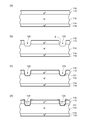
- the fourth embodiment is an embodiment according to a method for manufacturing a semiconductor device.
- the method for manufacturing a semiconductor device includes a first step of preparing a semiconductor element having a pn junction exposed portion where a pn junction is exposed, and a second step of forming a glass layer so as to cover the pn junction exposed portion. In this order. And in the said 2nd process, a glass layer is formed using the glass composition for semiconductor joining protection which concerns on Embodiment 1.
- FIG. 1 a semiconductor substrate having a pn junction parallel to the main surface is prepared, and a groove having a depth exceeding the pn junction is formed from one surface of the semiconductor substrate to expose the pn junction inside the groove.
- the second step includes a step of forming a glass layer so as to directly cover the pn junction exposed portion inside the groove.
- FIGS. 1 and 2 are views for explaining a method of manufacturing a semiconductor device according to the fourth embodiment.
- FIGS. 2A to 2D are process diagrams.
- the semiconductor device manufacturing method according to the fourth embodiment includes a “semiconductor substrate forming step”, a “groove forming step”, a “glass layer forming step”, a “photoresist forming step”, “ The “oxide film removing step”, “roughened region forming step”, “electrode forming step”, and “semiconductor substrate cutting step” are performed in this order.
- the method for manufacturing the semiconductor device according to the fourth embodiment will be described in the order of steps.
- p + -type diffusion layer 112 is diffused by diffusion of p-type impurities from one surface of n ⁇ -type semiconductor substrate (n ⁇ -type silicon substrate) 110, and n-type impurities from the other surface.
- An n + -type diffusion layer 114 is formed by diffusion to form a semiconductor substrate in which a pn junction parallel to the main surface is formed.
- oxide films 116 and 118 are formed on the surfaces of the p + type diffusion layer 112 and the n + type diffusion layer 114 by thermal oxidation (see FIG. 1A).
- (F) Roughened region forming step Next, a roughened surface for increasing the adhesion between the Ni-plated electrode and the semiconductor substrate by performing a roughening treatment on the surface of the semiconductor substrate in the portion 130 where the Ni-plated electrode film is formed.
- the formation region 132 is formed (see FIG. 2B).
- Electrode forming step Ni plating is performed on the semiconductor substrate to form the anode electrode 134 on the roughened region 132 and the cathode electrode 136 is formed on the other surface of the semiconductor substrate (FIG. 2C). )reference.).
- the high-breakdown-voltage mesa semiconductor device (semiconductor device according to the fourth embodiment) 100 can be manufactured.
- the fifth embodiment relates to a method for manufacturing a semiconductor device.
- the semiconductor device manufacturing method according to the fifth embodiment is similar to the semiconductor device manufacturing method according to the fourth embodiment.
- the first step is to prepare a semiconductor element having a pn junction exposed portion where the pn junction is exposed, and the pn junction exposure.
- a glass layer is formed using the glass composition for semiconductor joining protection which concerns on Embodiment 1.
- the first step includes a step of forming a pn junction exposed portion on the surface of the semiconductor substrate, and the second step includes a pn on the surface of the semiconductor substrate. Forming a glass layer so as to directly cover the joint exposed portion.
- FIGS. 3 and 4 are views for explaining the method for manufacturing the semiconductor device according to the fifth embodiment.
- 3A to FIG. 3C and FIG. 4A to FIG. 4C are process diagrams.
- the semiconductor device manufacturing method according to the fifth embodiment includes a “semiconductor substrate preparation step”, a “p + -type diffusion layer formation step”, an “n + -type diffusion layer formation step”, “ The “glass layer forming step”, “glass layer etching step”, “electrode forming step”, and “semiconductor substrate cutting step” are performed in this order.
- the semiconductor device manufacturing method according to the fifth embodiment will be described below in the order of steps.
- a p-type impurity for example, boron ions
- a p + type diffusion layer 214 is formed by thermal diffusion (see FIG. 3B).
- n + -type diffusion layer forming step Next, after removing the mask M1 and forming the mask M2, an n - type is formed on the surface of the n ⁇ -type epitaxial layer 212 via the mask M2 by ion implantation. Impurities (for example, arsenic ions) are introduced. Thereafter, an n + -type diffusion layer 216 is formed by thermal diffusion (see FIG. 3C).
- the high breakdown voltage planar semiconductor device (semiconductor device according to the fifth embodiment) 200 can be manufactured.
- the semiconductor device manufacturing method according to the sixth embodiment is similar to the semiconductor device manufacturing method according to the fourth embodiment.
- the first step is to prepare a semiconductor element having a pn junction exposed portion where the pn junction is exposed, and the pn junction exposure.
- a glass layer is formed using the glass composition for semiconductor joining protection which concerns on Embodiment 1.
- the second step forms an insulating layer on the exposed pn junction in the trench.
- a mesa-type pn diode is manufactured as the semiconductor device.
- FIGS. 5 and 6 are views for explaining the method for manufacturing the semiconductor device according to the sixth embodiment.
- 5 (a) to 5 (d) and FIGS. 6 (a) to 6 (d) are process diagrams.
- the method for manufacturing a semiconductor device according to the sixth embodiment includes a “semiconductor substrate forming step”, a “groove forming step”, an “insulating layer forming step”, a “glass layer forming step”, “ The “photoresist forming step”, “oxide film removing step”, “roughened region forming step”, “electrode forming step”, and “semiconductor substrate cutting step” are performed in this order.
- the semiconductor device manufacturing method according to the sixth embodiment will be described below in the order of steps.
- p + -type diffusion layer 112 is diffused by diffusion of p-type impurities from one surface of n ⁇ -type semiconductor substrate (n ⁇ -type silicon substrate) 110, and n-type impurities from the other surface.
- An n + -type diffusion layer 114 is formed by diffusion to form a semiconductor substrate in which a pn junction parallel to the main surface is formed.
- oxide films 116 and 118 are formed on the surfaces of the p + type diffusion layer 112 and the n + type diffusion layer 114 by thermal oxidation (see FIG. 5A).
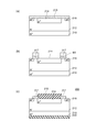
- an insulating layer 121 made of a silicon oxide film is formed on the inner surface of the groove 120 by a thermal oxidation method using dry oxygen (DryO 2 ) (see FIG. 5C).
- the thickness of the insulating layer 121 is in the range of 5 nm to 60 nm (for example, 20 nm).
- the insulating layer is formed by placing the semiconductor substrate in a diffusion furnace and then treating it at 900 ° C. for 10 minutes while flowing oxygen gas. If the thickness of the insulating layer 121 is less than 5 nm, the effect of reducing the reverse current may not be obtained. On the other hand, if the thickness of the insulating layer 121 exceeds 60 nm, a layer made of a glass composition may not be formed by electrophoresis in the next glass layer forming step.
- a layer made of the glass composition for protecting a semiconductor junction according to Embodiment 1 is formed on the inner surface of the groove 120 and the surface of the semiconductor substrate in the vicinity thereof by electrophoresis, and then the semiconductor junction A layer made of the protective glass composition is baked to form a passivation glass layer 124 (see FIG. 5D).
- a layer made of the glass composition for protecting a semiconductor junction is so formed as to cover the inner surface of the groove 120 with an insulating layer 121 interposed therebetween. Form. Therefore, the pn junction exposed portion A inside the groove 120 is covered with the glass layer 124 via the insulating layer 121.
- (F) Roughened region forming step Next, a roughened surface for increasing the adhesion between the Ni-plated electrode and the semiconductor substrate by performing a roughening treatment on the surface of the semiconductor substrate in the portion 130 where the Ni-plated electrode film is formed.
- the formation region 132 is formed (see FIG. 6B).
- a high-breakdown-voltage mesa semiconductor device semiconductor device according to Embodiment 6 102 can be manufactured.
- the semiconductor device manufacturing method according to the seventh embodiment is similar to the semiconductor device manufacturing method according to the fifth embodiment, in which a first step of preparing a semiconductor element having a pn junction exposed portion where a pn junction is exposed, and a pn junction exposure. And a second step of forming a glass layer so as to cover the part in this order. And in the said 2nd process, a glass layer is formed using the glass composition for semiconductor joining protection which concerns on Embodiment 1.
- the second step includes forming an insulating layer on the pn junction exposed portion on the surface of the semiconductor substrate. And a step of forming a glass layer so as to cover the pn junction exposed portion via the insulating layer.
- a planar pn diode is manufactured as the semiconductor device.
- FIG. 7 and 8 are views for explaining the method for manufacturing the semiconductor device according to the fifth embodiment.
- FIG. 7A to FIG. 7D and FIG. 8A to FIG. 8D are process diagrams.
- the semiconductor device manufacturing method according to the fifth embodiment includes a “semiconductor substrate preparation step”, a “p + -type diffusion layer formation step”, an “n + -type diffusion layer formation step”, “ The “insulating layer forming step”, “glass layer forming step”, “etching step”, “electrode forming step”, and “semiconductor substrate cutting step” are performed in this order.
- the semiconductor device manufacturing method according to the seventh embodiment will be described below in the order of steps.
- a p-type impurity for example, boron ions
- a p + type diffusion layer 214 is formed by thermal diffusion (see FIG. 7B).
- n + -type diffusion layer forming step Next, after removing the mask M1 and forming the mask M2, an n - type is formed on the surface of the n ⁇ -type epitaxial layer 212 via the mask M2 by ion implantation. Impurities (for example, arsenic ions) are introduced. Thereafter, an n + -type diffusion layer 216 is formed by thermal diffusion (see FIG. 7C). At this time, a pn junction exposed portion A is formed on the surface of the semiconductor substrate.
- Impurities for example, arsenic ions
- the thickness of the insulating layer 218 is less than 5 nm, the effect of reducing the reverse current may not be obtained. On the other hand, if the thickness of the insulating layer 218 exceeds 60 nm, a layer made of a glass composition may not be formed by electrophoresis in the next glass layer forming step.
- the high breakdown voltage planar semiconductor device (semiconductor device according to the seventh embodiment) 202 can be manufactured.
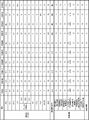
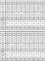
- FIG. 9 is a chart showing the conditions and results of the examples.
- the raw materials were prepared so that the composition ratios shown in Examples 1 to 8 and Comparative Examples 1 and 2 (see FIG. 9) were obtained, and after thoroughly stirring with a mixer, the mixed raw materials were heated to a predetermined temperature ( It was placed in a platinum crucible raised to 1350 ° C. to 1550 ° C. and melted for 2 hours. Thereafter, the melt was poured into a water-cooled roll to obtain flaky glass flakes. The glass flakes were pulverized with a ball mill until the average particle size became 5 ⁇ m to obtain a powdery glass composition.
- raw materials used in the examples are SiO 2, H 3 BO 3, Al 2 O 3, ZnO, CaCO 3, MgO, BaCO 3, NiO, ZrO 2 and PbO.
- Evaluation item 1 (environmental impact)
- the object of the present invention is “to make it possible to manufacture a semiconductor device having a high withstand voltage using a glass material containing no lead as in the case of using a conventional“ glass material mainly composed of lead silicate ”. Therefore, when the lead component is not included, an evaluation of “ ⁇ ” is given, and when the lead component is included, an evaluation of “x” is given.
- Evaluation item 2 (firing temperature) If the firing temperature is too high, the influence on the semiconductor device being manufactured increases. Therefore, when the firing temperature is 900 ° C. or lower, an evaluation of “O” is given, and when the firing temperature exceeds 900 ° C., Evaluation was given.
- Evaluation item 4 (average linear expansion coefficient) A flaky glass plate is prepared from the melt obtained in the above-mentioned section “1. Preparation of sample”, and the average linear expansion of the glass composition at 50 ° C. to 550 ° C. using the flaky glass plate. The rate was measured. The average linear expansion coefficient is measured using a thermomechanical analyzer TMA-60 manufactured by Shimadzu Corporation using a silicon single crystal having a length of 20 mm as a standard sample by a total expansion measurement method (temperature increase rate: 10 ° C./min). It was.
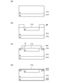
- FIG. 10 is a diagram illustrating an example of a measurement result of the average linear expansion coefficient.
- FIG. 10A is a diagram showing a measurement result in the glass composition for protecting a semiconductor junction according to Example 3
- FIG. 10B is a diagram showing a measurement result in the glass composition for protecting a semiconductor junction according to Comparative Example 1.
- FIG. When the difference between the average linear expansion coefficient of the glass composition at 50 ° C. to 550 ° C. and the linear expansion coefficient of silicon (3.73 ⁇ 10 ⁇ 6 ) is “0.4 ⁇ 10 ⁇ 6 ” or less, An evaluation was given, and an evaluation of “x” was given when the difference exceeded “0.4 ⁇ 10 ⁇ 6 ”.
- the numbers in parentheses indicate the average linear expansion coefficient of glass composition at 50 ° C. to 550 ° C. ⁇ 10 + 6 .
- Evaluation item 5 A semiconductor device (pn diode) was manufactured by the same method as the method for manufacturing a semiconductor device according to Embodiment 4 or 6, and the reverse characteristics of the manufactured semiconductor device were measured.
- a semiconductor device is manufactured by the method for manufacturing a semiconductor device according to Embodiment 4, and in Examples 1 to 6, the semiconductor device according to Embodiment 6 is manufactured.
- a semiconductor device was manufactured by the method. As a result, an evaluation of “ ⁇ ” was given when the reverse direction characteristic of the semiconductor device was in the normal range, and an evaluation of “X” was given when the reverse direction characteristic of the semiconductor device was not in the normal range.
- Evaluation item 6 Presence / absence of crystallization
- a semiconductor device (pn diode) was manufactured by the same method as the method for manufacturing a semiconductor device according to Embodiment 4 or 6.
- a semiconductor device is manufactured by the method for manufacturing a semiconductor device according to Embodiment 4, and in Examples 1 to 6, the semiconductor device according to Embodiment 6 is manufactured.
- a semiconductor device was manufactured by the method. As a result, in the process of vitrifying a layer composed of a glass composition, an evaluation of “ ⁇ ” is given if it can be vitrified without crystallization, and an evaluation of “x” if it cannot be vitrified by crystallization. Gave.
- Evaluation item 7 (whether or not bubbles are generated)
- a semiconductor device (pn diode) is manufactured by a method similar to the method for manufacturing a semiconductor device according to the fourth or sixth embodiment, and bubbles are formed inside the glass layer 124 (particularly, near the interface with the silicon substrate) during the vitrification process. Was observed (preliminary evaluation).
- a glass composition for protecting a semiconductor junction according to Examples 1 to 6 and Comparative Examples 1 and 2 is applied on a 10 mm square silicon substrate to form a layer made of the glass composition for protecting a semiconductor junction and the semiconductor junction.
- a layer made of the protective glass composition was fired to form a glass layer, and it was observed whether bubbles were generated inside the glass layer (particularly, in the vicinity of the interface with the semiconductor substrate) (this evaluation).
- a semiconductor device is manufactured by the method for manufacturing a semiconductor device according to Embodiment 4, and in Examples 1 to 6, the semiconductor device according to Embodiment 6 is manufactured.
- a semiconductor device was manufactured by the method.
- FIG. 11 is a diagram for explaining the bubbles b generated in the glass layer 124 in the preliminary evaluation.
- FIG. 11A is a cross-sectional view of the semiconductor device when the bubble b is not generated
- FIG. 11B is a cross-sectional view of the semiconductor device when the bubble b is generated.
- FIG. 12 is a photograph shown for explaining the bubbles b generated in the glass layer 124 in this evaluation.
- FIG. 12A is an enlarged view showing a boundary surface between the silicon substrate and the glass layer when the bubble b is not generated
- FIG. 12B is a diagram illustrating the silicon substrate and the glass when the bubble b is generated. It is a figure which expands and shows the interface with a layer.
- the glass compositions according to Examples 1 to 8 were evaluated as “ ⁇ ” for all the evaluation items (evaluation items 1 to 7).
- the glass compositions according to Examples 1 to 8 are all glass materials that do not contain lead, but (a) can be fired at an appropriate temperature (for example, 900 ° C. or lower), and are used in step (b).
- Resists chemicals (c) has a linear expansion coefficient close to that of silicon (especially the average linear expansion coefficient at 50 ° C to 550 ° C is close to that of silicon), and (d) excellent insulation All the conditions of having the property, and (e) not crystallizing in the process of vitrification, and (f) may occur from the interface with the silicon substrate in the process of forming the glass layer It turned out that it is a glass composition which suppresses generation
- the semiconductor device according to Examples 1 to 6 has a low reverse current regardless of the composition of the glass layer and the baking conditions, even in the case of the semiconductor device according to Examples 7 to 8.
- the semiconductor devices according to Examples 1 to 6 were more easily processed in the process of forming the glass layer by firing the layer made of the glass composition than the semiconductor devices according to Examples 7 to 8. It has also been found that bubbles are less likely to be generated from the interface between the substrate and the glass layer.
- FIG. 13 is a chart showing 18 levels of composition and results. From FIG. 13, the following items (1) to (4) were found.
- ⁇ tends to decrease as the sum of the content of SiO 2 and the content of B 2 O 3 increases. It was found that ⁇ tends to be smaller as the content of Al 2 O 3 is larger. As for ZnO, it was found that ⁇ tends to be smaller as the ZnO content is larger. This is because ⁇ is smaller due to crystallization. A smaller content is considered better.
- Ts tends to be lower when the sum of the content of SiO 2 and the content of B 2 O 3 is smaller, and the content of SiO 2 It was found that the larger the ratio of the content of B 2 O 3 to the amount, the lower the Ts, and the larger the BaO content, the lower the Ts.
- a glass composition that is basically based on the same composition as the glass composition for protecting a semiconductor junction according to Embodiment 1 but does not contain nickel oxide is used.
- this invention demonstrated the glass composition for semiconductor junction protection, this invention is not limited to this.
- a glass composition that is basically based on the same composition as the glass composition for protecting a semiconductor junction according to Embodiment 2 but does not contain nickel oxide is also included in the present invention.
- At least one metal oxide selected from the group consisting of nickel oxide, copper oxide, manganese oxide and zirconium oxide (foaming in the process of vitrification)
- nickel oxide was used as the “metal oxide having the property of suppressing generation”
- the present invention is not limited to this.
- copper oxide, manganese oxide, or zirconium oxide may be used instead of nickel oxide.
- the present invention relates to “a glass composition for protecting a semiconductor junction which substantially does not contain Pb, As, Sb, Li, Na, and K”.
- a glass composition for protecting a semiconductor junction which does not substantially contain Pb, P, As, Sb, Li, Na, and K is also included.
- the glass layer is formed using the glass composition for protecting a semiconductor junction according to Embodiment 1, but the present invention is not limited to this.
- the glass layer may be formed using the glass composition for protecting a semiconductor junction according to Embodiment 2 or 3.
- you may form a glass layer using the glass composition for another semiconductor junction protection which falls in the range of Claim 1 or 3.
- the present invention has been described by taking a diode (mesa type pn diode, planar type pn diode) as an example, but the present invention is not limited to this.
- the present invention can also be applied to all semiconductor devices (for example, thyristors, power MOSFETs, IGBTs, etc.) in which the pn junction is exposed.
Landscapes
- Engineering & Computer Science (AREA)
- Microelectronics & Electronic Packaging (AREA)
- Power Engineering (AREA)
- Condensed Matter Physics & Semiconductors (AREA)
- General Physics & Mathematics (AREA)
- Computer Hardware Design (AREA)
- Physics & Mathematics (AREA)
- Manufacturing & Machinery (AREA)
- Chemical & Material Sciences (AREA)
- Ceramic Engineering (AREA)
- Life Sciences & Earth Sciences (AREA)
- General Chemical & Material Sciences (AREA)
- Geochemistry & Mineralogy (AREA)
- Materials Engineering (AREA)
- Organic Chemistry (AREA)
- Chemical Kinetics & Catalysis (AREA)
- Glass Compositions (AREA)
- Formation Of Insulating Films (AREA)
Abstract
Description
従来の半導体装置の製造方法は、図14及び図15に示すように、「半導体基体形成工程」、「溝形成工程」、「ガラス層形成工程」、「フォトレジスト形成工程」、「酸化膜除去工程」、「粗面化領域形成工程」、「電極形成工程」及び「半導体基体切断工程」をこの順序で含む。以下、従来の半導体装置の製造方法を工程順に説明する。
まず、n-型半導体基板(n-型シリコン基板)910の一方の表面からのp型不純物の拡散によりp+型拡散層912、他方の表面からのn型不純物の拡散によりn+型拡散層914を形成して、主面に平行なpn接合が形成された半導体基体を形成する。その後、熱酸化によりp+型拡散層912及びn+型拡散層914の表面に酸化膜916,918を形成する(図14(a)参照。)。
次に、フォトエッチング法によって、酸化膜916の所定部位に所定の開口部を形成する。酸化膜のエッチング後、引き続いて半導体基体のエッチングを行い、半導体基体の一方の表面からpn接合を超える深さの溝920を形成する(図14(b)参照。)。
次に、溝920の表面に、電気泳動法により溝920の内面及びその近傍の半導体基体表面に半導体接合保護用ガラス組成物からなる層を形成するとともに、当該半導体接合保護用ガラス組成物からなる層を焼成することにより、パッシベーション用のガラス層924を形成する(図14(c)参照。)。
次に、ガラス層924の表面を覆うようにフォトレジスト926を形成する(図14(d)参照。)。
次に、フォトレジスト926をマスクとして酸化膜916のエッチングを行い、Niめっき電極膜を形成する部位930における酸化膜916,918を除去する(図15(a)参照。)。
次に、Niめっき電極膜を形成する部位930における半導体基体表面の粗面化処理を行い、Niめっき電極と半導体基体との密着性を高くするための粗面化領域932を形成する(図15(b)参照。)。
次に、半導体基体にNiめっきを行い、粗面化領域932上にアノード電極934を形成するとともに、半導体基体の他方の表面にカソード電極936を形成する(図15(c)参照。)。
次に、ダイシング等により、ガラス層924の中央部において半導体基体を切断して半導体基体をチップ化して、メサ型半導体装置(pnダイオード)900を作製する(図15(d)参照。)。
実施形態1は、半導体接合保護用ガラス組成物に係る実施形態である。
実施形態2は、半導体接合保護用ガラス組成物に係る実施形態である。
実施形態3は、半導体接合保護用ガラス組成物に係る実施形態である。
実施形態4は、半導体装置の製造方法に係る実施形態である。
実施形態4に係る半導体装置の製造方法は、図1及び図2に示すように、「半導体基体形成工程」、「溝形成工程」、「ガラス層形成工程」、「フォトレジスト形成工程」、「酸化膜除去工程」、「粗面化領域形成工程」、「電極形成工程」及び「半導体基体切断工程」をこの順序で実施する。以下、実施形態4に係る半導体装置の製造方法を工程順に説明する。
まず、n-型半導体基板(n-型シリコン基板)110の一方の表面からのp型不純物の拡散によりp+型拡散層112、他方の表面からのn型不純物の拡散によりn+型拡散層114を形成して、主面に平行なpn接合が形成された半導体基体を形成する。その後、熱酸化によりp+型拡散層112及びn+型拡散層114の表面に酸化膜116,118を形成する(図1(a)参照。)。
次に、フォトエッチング法によって、酸化膜116の所定部位に所定の開口部を形成する。酸化膜のエッチング後、引き続いて半導体基体のエッチングを行い、半導体基体の一方の表面からpn接合を超える深さの溝120を形成する(図1(b)参照。)。このとき、溝の内面にpn接合露出部Aが形成される。
次に、溝120の表面に、電気泳動法により溝120の内面及びその近傍の半導体基体表面に実施形態1に係る半導体接合保護用ガラス組成物からなる層を形成するとともに、当該半導体接合保護用ガラス組成物からなる層を焼成することにより、パッシベーション用のガラス層124を形成する(図1(c)参照。)。従って、溝120の内部におけるpn接合露出部はガラス層124により直接覆われた状態となる。
次に、ガラス層124の表面を覆うようにフォトレジスト126を形成する(図1(d)参照。)。
次に、フォトレジスト126をマスクとして酸化膜116のエッチングを行い、Niめっき電極膜を形成する部位130における酸化膜116,118を除去する(図2(a)参照。)。
次に、Niめっき電極膜を形成する部位130における半導体基体表面の粗面化処理を行い、Niめっき電極と半導体基体との密着性を高くするための粗面化領域132を形成する(図2(b)参照。)。
次に、半導体基体にNiめっきを行い、粗面化領域132上にアノード電極134を形成するとともに、半導体基体の他方の表面にカソード電極136を形成する(図2(c)参照。)。
次に、ダイシング等により、ガラス層124の中央部において半導体基体を切断して半導体基体をチップ化して、メサ型半導体装置(pnダイオード)を作製する(図2(d)参照。)。
実施形態5は、半導体装置の製造方法に係る実施形態である。
実施形態5に係る半導体装置の製造方法は、図3及び図4に示すように、「半導体基体準備工程」、「p+型拡散層形成工程」、「n+型拡散層形成工程」、「ガラス層形成工程」、「ガラス層エッチング工程」、「電極形成工程」及び「半導体基体切断工程」をこの順序で実施する。以下、実施形態5に係る半導体装置の製造方法を工程順に説明する。
まず、n+型シリコン基板210上にn-型エピタキシャル層212が積層された半導体基体を準備する(図3(a)参照。)。
次に、マスクM1を形成した後、当該マスクM1を介してn-型エピタキシャル層212の表面における所定領域にイオン注入法によりp型不純物(例えばボロンイオン)を導入する。その後、熱拡散することにより、p+型拡散層214を形成する(図3(b参照。)。
次に、マスクM1を除去するとともにマスクM2を形成した後、当該マスクM2を介してn-型エピタキシャル層212の表面における所定領域にイオン注入法によりn型不純物(例えばヒ素イオン)を導入する。その後、熱拡散することにより、n+型拡散層216を形成する(図3(c)参照。)。
次に、マスクM2を除去した後、n-型エピタキシャル層212の表面に、スピンコート法により、実施形態1に係る半導体接合保護用ガラス組成物からなる層を形成し、その後、当該半導体接合保護用ガラス組成物からなる層を焼成することにより、パッシベーション用のガラス層215を形成する(図4(a)参照。)。
次に、ガラス層215の表面にマスクM3を形成した後、ガラス層のエッチングを行う(図4(b)参照。)。これにより、n-型エピタキシャル層212の表面における所定領域にガラス層217が形成されることとなる。
次に、マスクM3を除去した後、半導体基体の表面におけるガラス層217で囲まれた領域にアノード電極218を形成するとともに、半導体基体の裏面にカソード電極220を形成する(図4(c)参照。)。
次に、ダイシング等により、半導体基体を切断して半導体基体をチップ化して、半導体装置(プレーナー型のpnダイオード)200を製造する(図示せず。)。
実施形態6に係る半導体装置の製造方法は、実施形態4に係る半導体装置の製造方法と同様に、pn接合が露出するpn接合露出部を有する半導体素子を準備する第1工程と、pn接合露出部を覆うようにガラス層を形成する第2工程とをこの順序で含む半導体装置の製造方法である。そして、当該第2工程においては、実施形態1に係る半導体接合保護用ガラス組成物を用いてガラス層を形成する。但し、実施形態6に係る半導体装置の製造方法においては、実施形態4に係る半導体装置の製造方法の場合とは異なり、第2工程が、溝の内部におけるpn接合露出部上に絶縁層を形成する工程と、当該絶縁層を介してpn接合露出部を覆うようにガラス層を形成する工程とを含む。実施形態6に係る半導体装置の製造方法においては、半導体装置としてメサ型のpnダイオードを製造する。
実施形態6に係る半導体装置の製造方法は、図5及び図6に示すように、「半導体基体形成工程」、「溝形成工程」、「絶縁層形成工程」、「ガラス層形成工程」、「フォトレジスト形成工程」、「酸化膜除去工程」、「粗面化領域形成工程」、「電極形成工程」及び「半導体基体切断工程」をこの順序で実施する。以下、実施形態6に係る半導体装置の製造方法を工程順に説明する。
まず、n-型半導体基板(n-型シリコン基板)110の一方の表面からのp型不純物の拡散によりp+型拡散層112、他方の表面からのn型不純物の拡散によりn+型拡散層114を形成して、主面に平行なpn接合が形成された半導体基体を形成する。その後、熱酸化によりp+型拡散層112及びn+型拡散層114の表面に酸化膜116,118を形成する(図5(a)参照。)。
次に、フォトエッチング法によって、酸化膜116の所定部位に所定の開口部を形成する。酸化膜のエッチング後、引き続いて半導体基体のエッチングを行い、半導体基体の一方の表面からpn接合を超える深さの溝120を形成する(図5(b)参照。)。このとき、溝の内面にpn接合露出部Aが形成される。
次に、ドライ酸素(DryO2)を用いた熱酸化法によって、溝120の内面にシリコン酸化膜からなる絶縁層121を形成する(図5(c)参照。)。絶縁層121の厚さは、5nm~60nmの範囲内(例えば20nm)とする。絶縁層の形成は、半導体基体を拡散炉に入れた後、酸素ガスを流しながら900℃の温度で10分処理することにより行う。絶縁層121の厚さが5nm未満であると逆方向電流低減の効果が得られなくなる場合がある。一方、絶縁層121の厚さが60nmを超えると次のガラス層形成工程で電気泳動法によりガラス組成物からなる層を形成することができなくなる場合がある。
次に、電気泳動法により溝120の内面及びその近傍の半導体基体表面に実施形態1に係る半導体接合保護用ガラス組成物からなる層を形成し、その後、当該半導体接合保護用ガラス組成物からなる層を焼成することにより、パッシベーション用のガラス層124を形成する(図5(d)参照。)。なお、溝120の内面に半導体接合保護用ガラス組成物からなる層を形成する際には、溝120の内面を絶縁層121を介して被覆するように半導体接合保護用ガラス組成物からなる層を形成する。従って、溝120の内部におけるpn接合露出部Aは絶縁層121を介してガラス層124により覆われた状態となる。
次に、ガラス層124の表面を覆うようにフォトレジスト126を形成した後、当該フォトレジスト126をマスクとして酸化膜116のエッチングを行い、Niめっき電極膜を形成する部位130における酸化膜116を除去する(図6(a)参照。)。
次に、Niめっき電極膜を形成する部位130における半導体基体表面の粗面化処理を行い、Niめっき電極と半導体基体との密着性を高くするための粗面化領域132を形成する(図6(b)参照。)。
次に、半導体基体にNiめっきを行い、粗面化領域132上にアノード電極134を形成するとともに、半導体基体の他方の表面にカソード電極136を形成する(図6(c)参照。)。
次に、ダイシング等により、ガラス層124の中央部において半導体基体を切断して半導体基体をチップ化して、半導体装置(メサ型のpnダイオード)102を作製する(図6(d)参照。)。
実施形態7に係る半導体装置の製造方法は、実施形態5に係る半導体装置の製造方法と同様に、pn接合が露出するpn接合露出部を有する半導体素子を準備する第1工程と、pn接合露出部を覆うようにガラス層を形成する第2工程とをこの順序で含む半導体装置の製造方法である。そして、当該第2工程においては、実施形態1に係る半導体接合保護用ガラス組成物を用いてガラス層を形成する。但し、実施形態7に係る半導体装置の製造方法においては、実施形態5に係る半導体装置の製造方法の場合とは異なり、第2工程が、半導体基体の表面におけるpn接合露出部上に絶縁層を形成する工程と、当該絶縁層を介してpn接合露出部を覆うようにガラス層を形成する工程とを含む。実施形態7に係る半導体装置の製造方法においては、半導体装置としてプレーナー型のpnダイオードを製造する。
実施形態5に係る半導体装置の製造方法は、図7及び図8に示すように、「半導体基体準備工程」、「p+型拡散層形成工程」、「n+型拡散層形成工程」、「絶縁層形成工程」、「ガラス層形成工程」、「エッチング工程」、「電極形成工程」及び「半導体基体切断工程」をこの順序で実施する。以下、実施形態7に係る半導体装置の製造方法を工程順に説明する。
まず、n+型シリコン基板210上にn-型エピタキシャル層212が積層された半導体基体を準備する(図7(a)参照。)。
次に、マスクM1を形成した後、当該マスクM1を介してn-型エピタキシャル層212の表面における所定領域にイオン注入法によりp型不純物(例えばボロンイオン)を導入する。その後、熱拡散することにより、p+型拡散層214を形成する(図7(b)参照。)。
次に、マスクM1を除去するとともにマスクM2を形成した後、当該マスクM2を介してn-型エピタキシャル層212の表面における所定領域にイオン注入法によりn型不純物(例えばヒ素イオン)を導入する。その後、熱拡散することにより、n+型拡散層216を形成する(図7(c)参照。)。このとき、半導体基体の表面にpn接合露出部Aが形成される。
次に、マスクM2を除去した後、ドライ酸素(DryO2)を用いた熱酸化法によって、n-型エピタキシャル層212の表面(及びn+型シリコン基板210の裏面)にシリコン酸化膜からなる絶縁層218を形成する(図7(d)参照。)。絶縁層218の厚さは、5nm~60nmの範囲内(例えば20nm)とする。絶縁層218の形成は、半導体基体を拡散炉に入れた後、酸素ガスを流しながら900℃の温度で10分処理することにより行う。絶縁層218の厚さが5nm未満であると逆方向電流低減の効果が得られなくなる場合がある。一方、絶縁層218の厚さが60nmを超えると次のガラス層形成工程で電気泳動法によりガラス組成物からなる層を形成することができなくなる場合がある。
次に、絶縁層218の表面に、電気泳動法により、実施形態1に係る半導体接合保護用ガラス組成物からなる層を形成し、その後、当該半導体接合保護用ガラス組成物からなる層を焼成することにより、パッシベーション用のガラス層220を形成する(図8(a)参照。)。
次に、ガラス層220の表面にマスクM3を形成した後、ガラス層220のエッチングを行い(図8(b)参照。)、引き続き、絶縁層218のエッチングを行う(図8(c)参照。)。これにより、n-型エピタキシャル層212の表面における所定領域に絶縁層218及びガラス層220が形成されることとなる。
次に、マスクM3を除去した後、半導体基体の表面におけるガラス層220で囲まれた領域にアノード電極222を形成するとともに、半導体基体の裏面にカソード電極224を形成する(図8(d)参照。)。
次に、ダイシング等により、半導体基体を切断して半導体基体をチップ化して、半導体装置(プレーナー型のpnダイオード)202を製造する(図示せず。)。
1.試料の調整
図9は、実施例の条件及び結果を示す図表である。実施例1~8及び比較例1~2に示す組成比(図9参照。)になるように原料を調合し、混合機でよく攪拌した後、その混合した原料を電気炉中で所定温度(1350℃~1550℃)まで上昇させた白金ルツボに入れ、2時間溶融させた。その後、融液を水冷ロールに流し出して薄片状のガラスフレークを得た。このガラスフレークをボールミルで平均粒径が5μmとなるまで粉砕して、粉末状のガラス組成物を得た。
上記方法により得た各ガラス組成物を用いて以下の評価項目により評価した。
本発明の目的が「鉛を含まないガラス材料を用いて、従来の『珪酸鉛を主成分としたガラス材料』を用いた場合と同様に高耐圧の半導体装置を製造することを可能とする」ことにあるため、鉛成分を含まない場合に「○」の評価を与え、鉛成分を含む場合に「×」の評価を与えた。
焼成温度が高すぎると製造中の半導体装置に与える影響が大きくなるため、焼成温度が900℃以下である場合に「○」の評価を与え、焼成温度が900℃を超える場合に「×」の評価を与えた。
ガラス組成物が王水及びめっき液の両方に対して難溶性を示す場合に「○」の評価を与え、王水及びめっき液の少なくとも一方に対して溶解性を示す場合に「×」の評価を与えた。
上記した「1.試料の調整」の欄で得られた融液から薄片状のガラス板を作製し、当該薄片状のガラス板を用いて、50℃~550℃におけるガラス組成物の平均線膨張率を測定した。平均線膨張率の測定は、島津製作所製の熱機械分析装置TMA-60を用いて、長さ20mmのシリコン単結晶を標準試料として、全膨張測定法(昇温速度10℃/分)により行った。
実施形態4又は6に係る半導体装置の製造方法と同様の方法によって半導体装置(pnダイオード)を作製し、作製した半導体装置の逆方向特性を測定した。なお、実施例7~8及び比較例1~2においては、実施形態4に係る半導体装置の製造方法によって半導体装置を作製し、実施例1~6においては、実施形態6に係る半導体装置の製造方法によって半導体装置を作製した。その結果、半導体装置の逆方向特性が正常範囲にある場合に「○」の評価を与え、半導体装置の逆方向特性が正常範囲にない場合に「×」の評価を与えた。
実施形態4又は6に係る半導体装置の製造方法と同様の方法によって半導体装置(pnダイオード)を作製した。なお、実施例7~8及び比較例1~2においては、実施形態4に係る半導体装置の製造方法によって半導体装置を作製し、実施例1~6においては、実施形態6に係る半導体装置の製造方法によって半導体装置を作製した。その結果、ガラス組成物からなる層をガラス化する過程で、結晶化することなくガラス化できた場合に「○」の評価を与え、結晶化によりガラス化できなかった場合に「×」の評価を与えた。
実施形態4又は6に係る半導体装置の製造方法と同様の方法によって半導体装置(pnダイオード)を作製し、ガラス化の過程でガラス層124の内部(特に、シリコン基板との境界面近傍)に泡が発生しているかどうかを観察した(予備評価)。また、10mm角のシリコン基板上に実施例1~6及び比較例1~2に係る半導体接合保護用ガラス組成物を塗布して半導体接合保護用ガラス組成物からなる層を形成するとともに当該半導体接合保護用ガラス組成物からなる層を焼成することによりガラス層を形成し、ガラス層の内部(特に、半導体基体との境界面近傍)に泡が発生しているかどうかを観察した(本評価)。なお、実施例7~8及び比較例1~2においては、実施形態4に係る半導体装置の製造方法によって半導体装置を作製し、実施例1~6においては、実施形態6に係る半導体装置の製造方法によって半導体装置を作製した。
上記した評価項目1~7についての各評価がすべて「○」の場合に「○」の評価を与え、各評価のうち1つでも「△」又は「×」がある場合に「×」の評価を与えた。
図9からも分かるように、比較例1~2に係るガラス組成物はいずれも、いずれかの評価項目で「×」の評価があり、「×」の総合評価が得られた。すなわち、比較例1に係るガラス組成物は、評価項目1及び4で「×」の評価が得られた。また、比較例2に係るガラス組成物は、評価項目3及び4で「×」の評価が得られた。
なお、上記の実施例1~8の組成を決定するにあたっては、18水準による予備実験を行い、この結果を参考にした。図13は、18水準の組成及び結果を示す図表である。図13から以下の(1)~(4)の事項が分かった。
Claims (20)
- 少なくともSiO2と、B2O3と、Al2O3と、ZnOと、CaO、MgO及びBaOのうち少なくとも2つのアルカリ土類金属の酸化物とを含有し、かつ、Pbと、Asと、Sbと、Liと、Naと、Kとを実質的に含有しない半導体接合保護用ガラス組成物であって、
50℃~550℃の温度範囲における平均線膨張率が3.33×10⁻⁶~4.13×10⁻⁶の範囲内にあることを特徴とする半導体接合保護用ガラス組成物。 - 50℃~550℃の温度範囲における平均線膨張率が3.38×10⁻⁶~4.08×10⁻⁶の範囲内にあることを特徴とする請求項1に記載の半導体接合保護用ガラス組成物。
- 少なくともSiO2と、B2O3と、Al2O3と、ZnOと、CaO、MgO及びBaOのうち少なくとも2つのアルカリ土類金属の酸化物とを含有し、かつ、Pbと、Asと、Sbと、Liと、Naと、Kとを実質的に含有しない半導体接合保護用ガラス組成物であって、
SiO2の含有量が49.5mol%~64.3mol%の範囲内にあり、
B2O3の含有量が8.4mol%~17.9mol%の範囲内にあり、
Al2O3の含有量が3.7mol%~14.8mol%の範囲内にあり、
ZnOの含有量が3.9mol%~14.2mol%の範囲内にあり、
アルカリ土類金属の酸化物の含有量が7.4mol%~12.9mol%の範囲内にあることを特徴とする半導体接合保護用ガラス組成物。 - SiO2の含有量とB2O3の含有量とを合計した値が、65mol%~75mol%の範囲内にあることを特徴とする請求項3に記載の半導体接合保護用ガラス組成物。
- 前記アルカリ土類金属の酸化物として、CaO、MgO及びBaOのすべてを含有することを特徴とする請求項1~4のいずれかに記載の半導体接合保護用ガラス組成物。
- CaO含有量が2.0mol%~5.3mol%の範囲内にあり、MgO含有量が1.0mol%~2.3mol%の範囲内にあり、BaO含有量が2.6mol%~5.3mol%の範囲内にあることを特徴とする請求項5に記載の半導体接合保護用ガラス組成物。
- 前記アルカリ土類金属の酸化物として、CaO及びBaOを含有することを特徴とする請求項1~4のいずれかに記載の半導体接合保護用ガラス組成物。
- 前記アルカリ土類金属の酸化物のうち、CaO含有量が2.0mol%~7.6mol%の範囲内にあり、BaO含有量が3.7mol%~5.9mol%の範囲内にあることを特徴とする請求項7に記載の半導体接合保護用ガラス組成物。
- ニッケル酸化物、銅酸化物、マンガン酸化物及びジルコニウム酸化物よりなる群から選択された少なくとも1つの金属酸化物をさらに含有することを特徴とする請求項1~8のいずれかに記載の半導体接合保護用ガラス組成物。
- ニッケル酸化物、銅酸化物、マンガン酸化物及びジルコニウム酸化物よりなる群から選択された少なくとも1つの金属酸化物の含有量が0.01mol%~2.0mol%の範囲内にあることを特徴とする請求項9に記載の半導体接合保護用ガラス組成物。
- pn接合が露出するpn接合露出部を有する半導体素子を準備する第1工程と、
前記pn接合露出部を覆うようにガラス層を形成する第2工程とをこの順序で含む半導体装置の製造方法であって、
前記第2工程においては、少なくともSiO2と、B2O3と、Al2O3と、ZnOと、CaO、MgO及びBaOのうち少なくとも2つのアルカリ土類金属の酸化物とを含有し、かつ、Pbと、Asと、Sbと、Liと、Naと、Kとを実質的に含有しない半導体接合保護用ガラス組成物であって、50℃~550℃の温度範囲における平均線膨率が3.33×10⁻⁶~4.13×10⁻⁶の範囲内にある半導体接合保護用ガラス組成物を用いて前記ガラス層を形成することを特徴とする半導体装置の製造方法。 - pn接合が露出するpn接合露出部を有する半導体素子を準備する第1工程と、
前記pn接合露出部を覆うようにガラス層を形成する第2工程とをこの順序で含む半導体装置の製造方法であって、
前記第2工程においては、少なくともSiO2と、B2O3と、Al2O3と、ZnOと、CaO、MgO及びBaOのうち少なくとも2つのアルカリ土類金属の酸化物とを含有し、かつ、Pbと、Asと、Sbと、Liと、Naと、Kとを実質的に含有しない半導体接合保護用ガラス組成物であって、SiO2の含有量が49.5mol%~64.3mol%の範囲内にあり、B2O3の含有量が8.4mol%~17.9mol%の範囲内にあり、Al2O3の含有量が3.7mol%~14.8mol%の範囲内にあり、ZnOの含有量が3.9mol%~14.2mol%の範囲内にあり、アルカリ土類金属の酸化物の含有量が7.4mol%~12.9mol%の範囲内にある半導体接合保護用ガラス組成物を用いて前記ガラス層を形成することを特徴とする半導体装置の製造方法。 - 前記第1工程は、主面に平行なpn接合を備える半導体基体を準備する工程と、前記半導体基体の一方の表面から前記pn接合を超える深さの溝を形成することにより、前記溝の内部に前記pn接合露出部を形成する工程とを含み、
前記第2工程は、前記溝の内部における前記pn接合露出部を覆うように前記ガラス層を形成する工程を含むことを特徴とする請求項11又は12に記載の半導体装置の製造方法。 - 前記第2工程は、前記溝の内部における前記pn接合露出部を直接覆うように前記ガラス層を形成する工程を含むことを特徴とする請求項13に記載の半導体装置の製造方法。
- 前記第2工程は、前記溝の内部における前記pn接合露出部上に絶縁層を形成する工程と、前記絶縁層を介して前記pn接合露出部を覆うように前記ガラス層を形成する工程とを含むことを特徴とする請求項13に記載の半導体装置の製造方法。
- 前記第1工程は、半導体基体の表面に前記pn接合露出部を形成する工程を含み、
前記第2工程は、前記半導体基体の表面における前記pn接合露出部を覆うように前記ガラス層を形成する工程を含むことを特徴とする請求項11又は12に記載の半導体装置の製造方法。 - 前記第2工程は、前記半導体基体の表面における前記pn接合露出部を直接覆うように前記ガラス層を形成する工程を含むことを特徴とする請求項16に記載の半導体装置の製造方法。
- 前記第2工程は、前記半導体基体の表面における前記pn接合露出部上に絶縁層を形成する工程と、前記絶縁層を介して前記pn接合露出部を覆うように前記ガラス層を形成する工程とを含むことを特徴とする請求項16に記載の半導体装置の製造方法。
- pn接合が露出するpn接合露出部を有する半導体素子と、
前記pn接合露出部を覆うように形成されたガラス層とを備える半導体装置であって、
前記ガラス層は、少なくともSiO2と、B2O3と、Al2O3と、ZnOと、CaO、MgO及びBaOのうち少なくとも2つのアルカリ土類金属の酸化物とを含有し、かつ、Pbと、Asと、Sbと、Liと、Naと、Kとを実質的に含有しない半導体接合保護用ガラス組成物であって、50℃~550℃の温度範囲における平均線膨率が3.33×10⁻⁶~4.13×10⁻⁶の範囲内にある半導体接合保護用ガラス組成物を用いて形成されたものであることを特徴とする半導体装置。 - pn接合が露出するpn接合露出部を有する半導体素子と、
前記pn接合露出部を覆うように形成されたガラス層とを備える半導体装置であって、
前記ガラス層は、少なくともSiO2と、B2O3と、Al2O3と、ZnOと、CaO、MgO及びBaOのうち少なくとも2つのアルカリ土類金属の酸化物とを含有し、かつ、Pbと、Asと、Sbと、Liと、Naと、Kとを実質的に含有しない半導体接合保護用ガラス組成物であって、SiO2の含有量が49.5mol%~64.3mol%の範囲内にあり、B2O3の含有量が8.4mol%~17.9mol%の範囲内にあり、Al2O3の含有量が3.7mol%~14.8mol%の範囲内にあり、ZnOの含有量が3.9mol%~14.2mol%の範囲内にあり、アルカリ土類金属の酸化物の含有量が7.4mol%~12.9mol%の範囲内にある半導体接合保護用ガラス組成物を用いて形成されたものであることを特徴とする半導体装置。
Priority Applications (6)
| Application Number | Priority Date | Filing Date | Title |
|---|---|---|---|
| US14/369,732 US9318401B2 (en) | 2012-05-08 | 2012-05-08 | Glass composition for protecting semiconductor junction, method of manufacturing semiconductor device and semiconductor device |
| JP2014514287A JP5827398B2 (ja) | 2012-05-08 | 2012-05-08 | 半導体接合保護用ガラス組成物の製造方法、半導体装置の製造方法及び半導体装置 |
| CN201280050753.2A CN103890919B (zh) | 2012-05-08 | 2012-05-08 | 半导体接合保护用玻璃复合物、半导体装置的制造方法以及半导体装置 |
| EP12876275.4A EP2849213B1 (en) | 2012-05-08 | 2012-05-08 | Glass composition for protecting semiconductor junction, method of manufacturing semiconductor device and semiconductor device |
| PCT/JP2012/061777 WO2013168237A1 (ja) | 2012-05-08 | 2012-05-08 | 半導体接合保護用ガラス組成物、半導体装置の製造方法及び半導体装置 |
| US15/063,420 US9698069B2 (en) | 2012-05-08 | 2016-03-07 | Glass composition for protecting semiconductor junction, method of manufacturing semiconductor device and semiconductor device |
Applications Claiming Priority (1)
| Application Number | Priority Date | Filing Date | Title |
|---|---|---|---|
| PCT/JP2012/061777 WO2013168237A1 (ja) | 2012-05-08 | 2012-05-08 | 半導体接合保護用ガラス組成物、半導体装置の製造方法及び半導体装置 |
Related Child Applications (2)
| Application Number | Title | Priority Date | Filing Date |
|---|---|---|---|
| US14/369,732 A-371-Of-International US9318401B2 (en) | 2012-05-08 | 2012-05-08 | Glass composition for protecting semiconductor junction, method of manufacturing semiconductor device and semiconductor device |
| US15/063,420 Continuation US9698069B2 (en) | 2012-05-08 | 2016-03-07 | Glass composition for protecting semiconductor junction, method of manufacturing semiconductor device and semiconductor device |
Publications (1)
| Publication Number | Publication Date |
|---|---|
| WO2013168237A1 true WO2013168237A1 (ja) | 2013-11-14 |
Family
ID=49550322
Family Applications (1)
| Application Number | Title | Priority Date | Filing Date |
|---|---|---|---|
| PCT/JP2012/061777 WO2013168237A1 (ja) | 2012-05-08 | 2012-05-08 | 半導体接合保護用ガラス組成物、半導体装置の製造方法及び半導体装置 |
Country Status (5)
| Country | Link |
|---|---|
| US (2) | US9318401B2 (ja) |
| EP (1) | EP2849213B1 (ja) |
| JP (1) | JP5827398B2 (ja) |
| CN (1) | CN103890919B (ja) |
| WO (1) | WO2013168237A1 (ja) |
Cited By (1)
| Publication number | Priority date | Publication date | Assignee | Title |
|---|---|---|---|---|
| US20160322512A1 (en) * | 2014-11-13 | 2016-11-03 | Shindengen Electric Manufacturing Co., Ltd. | Method of manufacturing semiconductor device and glass film forming apparatus |
Families Citing this family (9)
| Publication number | Priority date | Publication date | Assignee | Title |
|---|---|---|---|---|
| EP2717299B1 (en) | 2011-05-26 | 2016-07-27 | Shindengen Electric Manufacturing Co., Ltd. | Glass composition for semiconductor junction protection, production method for semiconductor device, and semiconductor device |
| WO2013168237A1 (ja) * | 2012-05-08 | 2013-11-14 | 新電元工業株式会社 | 半導体接合保護用ガラス組成物、半導体装置の製造方法及び半導体装置 |
| JP5508547B1 (ja) * | 2012-05-08 | 2014-06-04 | 新電元工業株式会社 | 半導体接合保護用ガラス組成物、半導体装置の製造方法及び半導体装置 |
| JP5631497B1 (ja) * | 2013-03-29 | 2014-11-26 | 新電元工業株式会社 | 半導体接合保護用ガラス組成物、半導体装置の製造方法及び半導体装置 |
| JP6588028B2 (ja) * | 2014-10-31 | 2019-10-09 | 新電元工業株式会社 | 半導体装置の製造方法及びレジストガラス |
| CN104599963B (zh) * | 2015-01-15 | 2017-12-19 | 苏州启澜功率电子有限公司 | 一种台面芯片双面电泳玻璃钝化工艺 |
| WO2018096643A1 (ja) * | 2016-11-25 | 2018-05-31 | 新電元工業株式会社 | 半導体装置の製造方法及び半導体装置 |
| JP7218531B2 (ja) * | 2018-10-04 | 2023-02-07 | 日本電気硝子株式会社 | 半導体素子被覆用ガラス及びこれを用いた半導体被覆用材料 |
| CN109755209A (zh) * | 2019-01-11 | 2019-05-14 | 常州星海电子股份有限公司 | 一种高可靠光阻玻璃钝化芯片及其加工方法 |
Citations (4)
| Publication number | Priority date | Publication date | Assignee | Title |
|---|---|---|---|---|
| JPS5336463A (en) * | 1976-09-16 | 1978-04-04 | Mitsubishi Electric Corp | Manufacture of semiconductor device |
| JP2002016272A (ja) * | 2000-06-30 | 2002-01-18 | Kyocera Corp | 光電変換装置 |
| JP2004087955A (ja) | 2002-08-28 | 2004-03-18 | Shindengen Electric Mfg Co Ltd | 半導体装置の製造方法及び半導体装置 |
| JP2006253669A (ja) * | 2005-02-09 | 2006-09-21 | Ngk Spark Plug Co Ltd | 配線基板 |
Family Cites Families (40)
| Publication number | Priority date | Publication date | Assignee | Title |
|---|---|---|---|---|
| GB1180908A (en) | 1966-11-17 | 1970-02-11 | English Electric Co Ltd | Improvements in or relating to processes for Forming an Insulating Coating on Silicon, and to Coated Silicon |
| JPS5240071A (en) | 1975-09-26 | 1977-03-28 | Hitachi Ltd | Semiconductor device |
| DE2730130C2 (de) | 1976-09-14 | 1987-11-12 | Mitsubishi Denki K.K., Tokyo | Verfahren zum Herstellen von Halbleiterbauelementen |
| JPS5393783A (en) | 1977-01-26 | 1978-08-17 | Nec Home Electronics Ltd | Mesa type semiconductor device |
| JPS5526656A (en) * | 1978-08-17 | 1980-02-26 | Hitachi Ltd | Semiconductor element coverd with glass |
| JPS5571646A (en) * | 1978-11-24 | 1980-05-29 | Hitachi Ltd | Glass composition |
| JPS56104443A (en) * | 1980-01-23 | 1981-08-20 | Hitachi Ltd | Manufacture of semiconductor device |
| JPS57202742A (en) * | 1981-06-09 | 1982-12-11 | Toshiba Corp | Glass for semiconductor coating |
| JPS5855345A (ja) * | 1981-09-30 | 1983-04-01 | Hitachi Ltd | 半導体装置用ガラス組成物 |
| US5298330A (en) * | 1987-08-31 | 1994-03-29 | Ferro Corporation | Thick film paste compositions for use with an aluminum nitride substrate |
| JPH01186629A (ja) | 1988-01-14 | 1989-07-26 | Rohm Co Ltd | メサ型半導体素子の製造方法 |
| JPH02163938A (ja) * | 1988-12-16 | 1990-06-25 | Fuji Electric Co Ltd | 半導体素子の製造方法 |
| US5047369A (en) * | 1989-05-01 | 1991-09-10 | At&T Bell Laboratories | Fabrication of semiconductor devices using phosphosilicate glasses |
| JPH05336463A (ja) | 1992-06-03 | 1993-12-17 | Sony Corp | テレビジョン受像機 |
| US5433794A (en) | 1992-12-10 | 1995-07-18 | Micron Technology, Inc. | Spacers used to form isolation trenches with improved corners |
| JP3339549B2 (ja) | 1996-10-14 | 2002-10-28 | 株式会社日立製作所 | ガラス被覆半導体装置及びその製造方法 |
| JP3780061B2 (ja) * | 1997-04-17 | 2006-05-31 | 株式会社日立製作所 | 面実装型半導体装置 |
| US5998037A (en) | 1997-12-22 | 1999-12-07 | Ferro Corporation | Porcelain enamel composition for electronic applications |
| US6171987B1 (en) | 1997-12-29 | 2001-01-09 | Ben-Gurion University Of The Negev | Cadmium-free and lead-free glass compositions, thick film formulations containing them and uses thereof |
| US6620996B2 (en) | 2000-05-29 | 2003-09-16 | Kyocera Corporation | Photoelectric conversion device |
| JP2002190553A (ja) * | 2000-12-21 | 2002-07-05 | Toshiba Components Co Ltd | 樹脂封止型半導体素子及びその製造方法 |
| JP2003267750A (ja) * | 2002-03-15 | 2003-09-25 | Nihon Yamamura Glass Co Ltd | 抵抗体被覆用ガラス組成物 |
| US7740899B2 (en) | 2002-05-15 | 2010-06-22 | Ferro Corporation | Electronic device having lead and cadmium free electronic overglaze applied thereto |
| JP4736342B2 (ja) * | 2004-04-09 | 2011-07-27 | 株式会社村田製作所 | ガラスセラミック原料組成物、ガラスセラミック焼結体およびガラスセラミック多層基板 |
| TWI414218B (zh) | 2005-02-09 | 2013-11-01 | Ngk Spark Plug Co | 配線基板及配線基板內建用之電容器 |
| JP4697397B2 (ja) * | 2005-02-16 | 2011-06-08 | サンケン電気株式会社 | 複合半導体装置 |
| DE102006023115A1 (de) * | 2006-05-16 | 2007-11-22 | Schott Ag | Backlightsystem mit IR-Absorptionseigenschaften |
| DE102006062428B4 (de) | 2006-12-27 | 2012-10-18 | Schott Ag | Verfahren zur Herstellung eines mit einem bleifreien Glas passiviertenelektronischen Bauelements sowie elektronisches Bauelement mit aufgebrachtem bleifreien Glas und dessen Verwendung |
| JP5365517B2 (ja) | 2007-08-01 | 2013-12-11 | 旭硝子株式会社 | 無鉛ガラス |
| JP5128203B2 (ja) | 2007-08-22 | 2013-01-23 | 日本山村硝子株式会社 | 封着用ガラス組成物 |
| JP5526656B2 (ja) | 2009-08-25 | 2014-06-18 | 株式会社Ihi | 防護装置及び燃焼試験設備 |
| JP2011060857A (ja) * | 2009-09-07 | 2011-03-24 | Hitachi Maxell Ltd | 集光型光発電モジュール及び集光型光発電モジュールの製造方法 |
| JP5565747B2 (ja) * | 2010-01-28 | 2014-08-06 | 日本電気硝子株式会社 | 半導体被覆用ガラスおよびそれを用いてなる半導体被覆用材料 |
| US20120052275A1 (en) * | 2010-08-30 | 2012-03-01 | Avanstrate Inc. | Glass substrate, chemically strengthened glass substrate and cover glass, and method for manufactruing the same |
| JP5336463B2 (ja) * | 2010-12-22 | 2013-11-06 | 住友建機株式会社 | 特殊アスファルト合材用アスファルトフィニッシャ |
| CN103189990A (zh) * | 2011-10-28 | 2013-07-03 | 松下电器产业株式会社 | 薄膜半导体器件及其制造方法 |
| US20140352778A1 (en) | 2011-12-22 | 2014-12-04 | Heraeus Precious Metals North America Conshohocken Llc | Solar cell pastes for low resistance contacts |
| CN103403846B (zh) * | 2012-01-31 | 2016-07-06 | 新电元工业株式会社 | 半导体接合保护用玻璃复合物、半导体装置的制造方法及半导体装置 |
| WO2013168237A1 (ja) * | 2012-05-08 | 2013-11-14 | 新電元工業株式会社 | 半導体接合保護用ガラス組成物、半導体装置の製造方法及び半導体装置 |
| EP2858098B1 (en) * | 2012-05-08 | 2020-12-02 | Shindengen Electric Manufacturing Co., Ltd. | Method of manufacturing a resin-sealed semiconductor device |
-
2012
- 2012-05-08 WO PCT/JP2012/061777 patent/WO2013168237A1/ja active Application Filing
- 2012-05-08 JP JP2014514287A patent/JP5827398B2/ja active Active
- 2012-05-08 CN CN201280050753.2A patent/CN103890919B/zh active Active
- 2012-05-08 EP EP12876275.4A patent/EP2849213B1/en active Active
- 2012-05-08 US US14/369,732 patent/US9318401B2/en active Active
-
2016
- 2016-03-07 US US15/063,420 patent/US9698069B2/en active Active
Patent Citations (4)
| Publication number | Priority date | Publication date | Assignee | Title |
|---|---|---|---|---|
| JPS5336463A (en) * | 1976-09-16 | 1978-04-04 | Mitsubishi Electric Corp | Manufacture of semiconductor device |
| JP2002016272A (ja) * | 2000-06-30 | 2002-01-18 | Kyocera Corp | 光電変換装置 |
| JP2004087955A (ja) | 2002-08-28 | 2004-03-18 | Shindengen Electric Mfg Co Ltd | 半導体装置の製造方法及び半導体装置 |
| JP2006253669A (ja) * | 2005-02-09 | 2006-09-21 | Ngk Spark Plug Co Ltd | 配線基板 |
Cited By (2)
| Publication number | Priority date | Publication date | Assignee | Title |
|---|---|---|---|---|
| US20160322512A1 (en) * | 2014-11-13 | 2016-11-03 | Shindengen Electric Manufacturing Co., Ltd. | Method of manufacturing semiconductor device and glass film forming apparatus |
| US9978882B2 (en) * | 2014-11-13 | 2018-05-22 | Shindengen Electric Manufacturing Co., Ltd. | Method of manufacturing semiconductor device and glass film forming apparatus |
Also Published As
| Publication number | Publication date |
|---|---|
| US20140353851A1 (en) | 2014-12-04 |
| US9698069B2 (en) | 2017-07-04 |
| US20160190026A1 (en) | 2016-06-30 |
| EP2849213A4 (en) | 2015-11-18 |
| EP2849213A1 (en) | 2015-03-18 |
| CN103890919A (zh) | 2014-06-25 |
| US9318401B2 (en) | 2016-04-19 |
| JP5827398B2 (ja) | 2015-12-02 |
| CN103890919B (zh) | 2016-07-06 |
| EP2849213B1 (en) | 2017-04-19 |
| JPWO2013168237A1 (ja) | 2015-12-24 |
Similar Documents
| Publication | Publication Date | Title |
|---|---|---|
| JP5827398B2 (ja) | 半導体接合保護用ガラス組成物の製造方法、半導体装置の製造方法及び半導体装置 | |
| JP4927237B1 (ja) | 半導体接合保護用ガラス組成物、半導体装置の製造方法及び半導体装置 | |
| JP5340511B1 (ja) | 半導体装置の製造方法及び半導体装置 | |
| JP5548276B2 (ja) | 半導体接合保護用ガラス組成物、半導体装置の製造方法及び半導体装置 | |
| WO2014155739A1 (ja) | 半導体接合保護用ガラス組成物、半導体装置の製造方法及び半導体装置 | |
| JP5508547B1 (ja) | 半導体接合保護用ガラス組成物、半導体装置の製造方法及び半導体装置 | |
| JP5184717B1 (ja) | 半導体接合保護用ガラス組成物、半導体装置の製造方法及び半導体装置 | |
| WO2012160961A1 (ja) | 半導体装置の製造方法及び半導体装置 | |
| JP5833112B2 (ja) | ガラス組成物の製造方法 | |
| JP4993399B1 (ja) | 半導体接合保護用ガラス組成物、半導体装置の製造方法及び半導体装置 | |
| JP5655140B2 (ja) | 半導体装置の製造方法及び半導体装置 | |
| JP5139596B2 (ja) | 半導体接合保護用ガラス組成物、半導体装置の製造方法及び半導体装置 | |
| JP5848821B2 (ja) | 半導体接合保護用ガラス組成物、半導体装置の製造方法、半導体装置及び半導体接合保護用ガラス組成物の製造方法 | |
| JP5655139B2 (ja) | 半導体装置の製造方法及び半導体装置 |
Legal Events
| Date | Code | Title | Description |
|---|---|---|---|
| ENP | Entry into the national phase |
Ref document number: 2014514287 Country of ref document: JP Kind code of ref document: A |
|
| 121 | Ep: the epo has been informed by wipo that ep was designated in this application |
Ref document number: 12876275 Country of ref document: EP Kind code of ref document: A1 |
|
| WWE | Wipo information: entry into national phase |
Ref document number: 14369732 Country of ref document: US |
|
| REEP | Request for entry into the european phase |
Ref document number: 2012876275 Country of ref document: EP |
|
| WWE | Wipo information: entry into national phase |
Ref document number: 2012876275 Country of ref document: EP |
|
| NENP | Non-entry into the national phase |
Ref country code: DE |