WO2013157335A1 - 半導体デバイスの製造方法 - Google Patents
半導体デバイスの製造方法 Download PDFInfo
- Publication number
- WO2013157335A1 WO2013157335A1 PCT/JP2013/057312 JP2013057312W WO2013157335A1 WO 2013157335 A1 WO2013157335 A1 WO 2013157335A1 JP 2013057312 W JP2013057312 W JP 2013057312W WO 2013157335 A1 WO2013157335 A1 WO 2013157335A1
- Authority
- WO
- WIPO (PCT)
- Prior art keywords
- electrode
- schottky
- surface electrode
- semiconductor device
- layer
- Prior art date
- Legal status (The legal status is an assumption and is not a legal conclusion. Google has not performed a legal analysis and makes no representation as to the accuracy of the status listed.)
- Ceased
Links
Images








Classifications
-
- H—ELECTRICITY
- H10—SEMICONDUCTOR DEVICES; ELECTRIC SOLID-STATE DEVICES NOT OTHERWISE PROVIDED FOR
- H10D—INORGANIC ELECTRIC SEMICONDUCTOR DEVICES
- H10D64/00—Electrodes of devices having potential barriers
- H10D64/01—Manufacture or treatment
- H10D64/012—Manufacture or treatment of electrodes comprising a Schottky barrier to a semiconductor
- H10D64/0121—Manufacture or treatment of electrodes comprising a Schottky barrier to a semiconductor to Group IV semiconductors
-
- H—ELECTRICITY
- H10—SEMICONDUCTOR DEVICES; ELECTRIC SOLID-STATE DEVICES NOT OTHERWISE PROVIDED FOR
- H10D—INORGANIC ELECTRIC SEMICONDUCTOR DEVICES
- H10D62/00—Semiconductor bodies, or regions thereof, of devices having potential barriers
- H10D62/10—Shapes, relative sizes or dispositions of the regions of the semiconductor bodies; Shapes of the semiconductor bodies
- H10D62/102—Constructional design considerations for preventing surface leakage or controlling electric field concentration
- H10D62/103—Constructional design considerations for preventing surface leakage or controlling electric field concentration for increasing or controlling the breakdown voltage of reverse-biased devices
- H10D62/105—Constructional design considerations for preventing surface leakage or controlling electric field concentration for increasing or controlling the breakdown voltage of reverse-biased devices by having particular doping profiles, shapes or arrangements of PN junctions; by having supplementary regions, e.g. junction termination extension [JTE]
- H10D62/106—Constructional design considerations for preventing surface leakage or controlling electric field concentration for increasing or controlling the breakdown voltage of reverse-biased devices by having particular doping profiles, shapes or arrangements of PN junctions; by having supplementary regions, e.g. junction termination extension [JTE] having supplementary regions doped oppositely to or in rectifying contact with regions of the semiconductor bodies, e.g. guard rings with PN or Schottky junctions
-
- H—ELECTRICITY
- H10—SEMICONDUCTOR DEVICES; ELECTRIC SOLID-STATE DEVICES NOT OTHERWISE PROVIDED FOR
- H10D—INORGANIC ELECTRIC SEMICONDUCTOR DEVICES
- H10D62/00—Semiconductor bodies, or regions thereof, of devices having potential barriers
- H10D62/80—Semiconductor bodies, or regions thereof, of devices having potential barriers characterised by the materials
- H10D62/83—Semiconductor bodies, or regions thereof, of devices having potential barriers characterised by the materials being Group IV materials, e.g. B-doped Si or undoped Ge
- H10D62/832—Semiconductor bodies, or regions thereof, of devices having potential barriers characterised by the materials being Group IV materials, e.g. B-doped Si or undoped Ge being Group IV materials comprising two or more elements, e.g. SiGe
- H10D62/8325—Silicon carbide
-
- H—ELECTRICITY
- H10—SEMICONDUCTOR DEVICES; ELECTRIC SOLID-STATE DEVICES NOT OTHERWISE PROVIDED FOR
- H10D—INORGANIC ELECTRIC SEMICONDUCTOR DEVICES
- H10D64/00—Electrodes of devices having potential barriers
- H10D64/01—Manufacture or treatment
- H10D64/011—Manufacture or treatment of electrodes ohmically coupled to a semiconductor
- H10D64/0111—Manufacture or treatment of electrodes ohmically coupled to a semiconductor to Group IV semiconductors
- H10D64/0112—Manufacture or treatment of electrodes ohmically coupled to a semiconductor to Group IV semiconductors using conductive layers comprising silicides
-
- H—ELECTRICITY
- H10—SEMICONDUCTOR DEVICES; ELECTRIC SOLID-STATE DEVICES NOT OTHERWISE PROVIDED FOR
- H10D—INORGANIC ELECTRIC SEMICONDUCTOR DEVICES
- H10D64/00—Electrodes of devices having potential barriers
- H10D64/01—Manufacture or treatment
- H10D64/012—Manufacture or treatment of electrodes comprising a Schottky barrier to a semiconductor
- H10D64/0121—Manufacture or treatment of electrodes comprising a Schottky barrier to a semiconductor to Group IV semiconductors
- H10D64/0123—Manufacture or treatment of electrodes comprising a Schottky barrier to a semiconductor to Group IV semiconductors to silicon carbide
-
- H—ELECTRICITY
- H10—SEMICONDUCTOR DEVICES; ELECTRIC SOLID-STATE DEVICES NOT OTHERWISE PROVIDED FOR
- H10D—INORGANIC ELECTRIC SEMICONDUCTOR DEVICES
- H10D64/00—Electrodes of devices having potential barriers
- H10D64/60—Electrodes characterised by their materials
- H10D64/62—Electrodes ohmically coupled to a semiconductor
-
- H—ELECTRICITY
- H10—SEMICONDUCTOR DEVICES; ELECTRIC SOLID-STATE DEVICES NOT OTHERWISE PROVIDED FOR
- H10D—INORGANIC ELECTRIC SEMICONDUCTOR DEVICES
- H10D64/00—Electrodes of devices having potential barriers
- H10D64/60—Electrodes characterised by their materials
- H10D64/64—Electrodes comprising a Schottky barrier to a semiconductor
-
- H—ELECTRICITY
- H10—SEMICONDUCTOR DEVICES; ELECTRIC SOLID-STATE DEVICES NOT OTHERWISE PROVIDED FOR
- H10D—INORGANIC ELECTRIC SEMICONDUCTOR DEVICES
- H10D8/00—Diodes
- H10D8/01—Manufacture or treatment
- H10D8/051—Manufacture or treatment of Schottky diodes
-
- H—ELECTRICITY
- H10—SEMICONDUCTOR DEVICES; ELECTRIC SOLID-STATE DEVICES NOT OTHERWISE PROVIDED FOR
- H10D—INORGANIC ELECTRIC SEMICONDUCTOR DEVICES
- H10D8/00—Diodes
- H10D8/60—Schottky-barrier diodes
-
- H—ELECTRICITY
- H10—SEMICONDUCTOR DEVICES; ELECTRIC SOLID-STATE DEVICES NOT OTHERWISE PROVIDED FOR
- H10P—GENERIC PROCESSES OR APPARATUS FOR THE MANUFACTURE OR TREATMENT OF DEVICES COVERED BY CLASS H10
- H10P14/00—Formation of materials, e.g. in the shape of layers or pillars
- H10P14/40—Formation of materials, e.g. in the shape of layers or pillars of conductive or resistive materials
- H10P14/42—Formation of materials, e.g. in the shape of layers or pillars of conductive or resistive materials using a gas or vapour
- H10P14/44—Physical vapour deposition [PVD]
-
- H—ELECTRICITY
- H10—SEMICONDUCTOR DEVICES; ELECTRIC SOLID-STATE DEVICES NOT OTHERWISE PROVIDED FOR
- H10W—GENERIC PACKAGES, INTERCONNECTIONS, CONNECTORS OR OTHER CONSTRUCTIONAL DETAILS OF DEVICES COVERED BY CLASS H10
- H10W72/00—Interconnections or connectors in packages
- H10W72/90—Bond pads, in general
- H10W72/921—Structures or relative sizes of bond pads
- H10W72/923—Bond pads having multiple stacked layers
-
- H—ELECTRICITY
- H10—SEMICONDUCTOR DEVICES; ELECTRIC SOLID-STATE DEVICES NOT OTHERWISE PROVIDED FOR
- H10W—GENERIC PACKAGES, INTERCONNECTIONS, CONNECTORS OR OTHER CONSTRUCTIONAL DETAILS OF DEVICES COVERED BY CLASS H10
- H10W72/00—Interconnections or connectors in packages
- H10W72/90—Bond pads, in general
- H10W72/951—Materials of bond pads
- H10W72/952—Materials of bond pads comprising metals or metalloids, e.g. PbSn, Ag or Cu
Definitions
- the present invention relates to a method for manufacturing a semiconductor device.
- the present invention relates to a method for manufacturing a semiconductor device having an electrode structure having an appropriate reflectivity and not causing voids.
- SiC silicon carbide
- the structure of the power device is mainly a vertical semiconductor device having a back electrode with a low-resistance ohmic electrode on the back side.
- Various materials and structures are used for the back electrode, and one of them is a laminate of a titanium layer, a nickel layer, and a silver layer (see, for example, Patent Document 1 below), a titanium layer, A laminate of a nickel layer and a gold layer (see, for example, Patent Document 2 below) has been proposed.
- a nickel layer is formed on a SiC substrate, and then a nickel silicide layer is formed by heating, so that the SiC substrate and the nickel silicide layer are interposed between them.
- a method of forming an ohmic contact is used (for example, see Patent Documents 1 and 2 below).
- a film made of a plurality of metals is formed on a SiC substrate, and then heat treatment is performed at 700 ° C. to 1100 ° C., and most preferably, ohmic characteristics can be obtained at about 800 ° C.
- heat treatment is performed at 700 ° C. to 1100 ° C., and most preferably, ohmic characteristics can be obtained at about 800 ° C.
- Patent Document 4 a technique for forming an ohmic electrode by irradiating a laser beam has been proposed (see, for example, Patent Document 4 below).
- a metal layer made of aluminum or an aluminum alloy is formed on the Schottky contact to form an electrode structure. If it is not completely covered, voids are generated, causing a device failure.
- the surface electrode of the SiC semiconductor is required to have good coverage with respect to the pattern irregularities of the Schottky contact (Schottky electrode).
- the surface electrode is required to be formed so as to have an optimum reflectance for positioning image recognition when performing automatic wire bonding.
- an object of the present invention is to provide a method for manufacturing a semiconductor device having good coverage with respect to the unevenness of a Schottky contact. It is another object of the present invention to provide a method for manufacturing a semiconductor device that can form a surface electrode having an optimal reflectance for image recognition such as positioning.
- a method for manufacturing a semiconductor device is a method for manufacturing a semiconductor device in which an electrode structure is formed on a silicon carbide semiconductor substrate, and has the following characteristics.
- a Schottky layer containing any one of titanium, tungsten, molybdenum, and chromium is formed on the front surface of the silicon carbide semiconductor substrate.
- the Schottky layer is heated to form a Schottky electrode having a Schottky contact with the silicon carbide semiconductor substrate.
- a surface electrode is formed on the surface of the Schottky electrode by using aluminum or aluminum containing silicon.
- the surface electrode is heated with a temperature range suitable for the condition that the unevenness of the Schottky electrode is excellent and the surface electrode has a predetermined reflectance or less.
- the surface electrode is formed by a sputtering method, the pressure during sputtering is 0.1 Pa or more and 1 Pa or less, and the temperature of the silicon carbide semiconductor substrate is 100 ° C. or more and 500 ° C. It is characterized by being below °C.
- the heating is performed in a temperature range having a condition that the reflectance of the surface electrode is 80% or less.
- a back electrode structure comprising an ohmic electrode of a nickel silicide layer containing titanium carbide and a back electrode of a metal layer is formed on the back side of the silicon carbide semiconductor substrate.
- a layer containing titanium is formed on a silicon carbide semiconductor substrate, and after forming a Schottky contact by heating, aluminum or aluminum containing silicon is formed as a surface electrode.
- the surface electrode is formed by sputtering, the surface electrode has good coverage with respect to the irregularities on the surface of the Schottky electrode when the relationship between the sputtering pressure and the sputtering temperature is a predetermined condition.
- the surface electrode can obtain an optimal reflectance for image recognition when performing automatic wire bonding.
- FIG. 1 is a cross-sectional view showing a Schottky barrier diode according to an embodiment of a semiconductor device of the present invention.
- FIG. 2 is a cross-sectional view for explaining the manufacturing method of the Schottky barrier diode (No. 1).
- FIG. 3 is a cross-sectional view for explaining the manufacturing method of the Schottky barrier diode (No. 2).
- FIG. 4 is a cross-sectional view for explaining the manufacturing method of the Schottky barrier diode (No. 3).
- FIG. 5 is a sectional view for explaining the method for producing the Schottky barrier diode (No. 4).
- FIG. 6 is a sectional view for explaining the method for producing the Schottky barrier diode (part 5).
- FIG. 1 is a cross-sectional view showing a Schottky barrier diode according to an embodiment of a semiconductor device of the present invention.
- FIG. 2 is a cross-sectional view for explaining the manufacturing method of the
- FIG. 7 is a cross-sectional view for explaining the manufacturing method of the Schottky barrier diode (No. 6).
- FIG. 8 is a cross-sectional view for explaining the manufacturing method of the Schottky barrier diode (No. 7).
- FIG. 9 is a sectional view for explaining the method for producing the Schottky barrier diode (No. 8).
- FIG. 10 is a cross-sectional view illustrating a Schottky barrier diode having a field limiting ring structure according to an embodiment of the present invention.
- FIG. 11 is a cross-sectional view illustrating a Schottky barrier diode having a junction barrier Schottky structure according to an embodiment of the present invention.
- FIG. 12 is a chart showing the relationship between the temperature and the reflectance when forming the surface electrode according to the present invention.
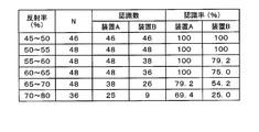
- FIG. 13 is a chart showing the relationship between the reflectance of the surface electrode in the SiC semiconductor device of the present invention and the recognition rate in the automatic wire bonding apparatus (part 1).
- FIG. 14 is a chart showing the relationship between the reflectance of the surface electrode in the SiC semiconductor device of the present invention and the recognition rate in the automatic wire bonding apparatus (part 2).
- a nickel silicide layer containing titanium carbide is referred to as an ohmic electrode
- a metal layer laminated on the ohmic electrode is referred to as a back electrode
- a structure including the ohmic electrode and the back electrode is referred to as a back electrode structure.
- SiC silicon carbide
- a Schottky electrode in contact with the SiC substrate and a surface electrode (front surface electrode) made of a metal layer on the surface of the Schottky electrode are provided. Form and provide.
- a structure composed of a Schottky electrode and a surface electrode is called a surface electrode structure.
- a layer containing a titanium carbide layer formed by heating a layer containing nickel and titanium is excellent in adhesion to the nickel silicide layer and adhesion to the titanium layer used in the back electrode.
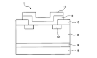
- FIG. 1 is a cross-sectional view showing a Schottky barrier diode according to an embodiment of a semiconductor device of the present invention.
- a Schottky barrier diode 1 as an SiC semiconductor device, a SiC substrate 11 and a guard ring 12, an insulating layer 13, a Schottky electrode 16, and a surface electrode 17 are formed on the front surface side of the SiC substrate 11.
- a nickel silicide layer 14 including a titanium carbide and a back electrode 18 are formed on the back surface side of the SiC substrate 11.
- FIGS. 2 to 9 are cross-sectional views illustrating a method for manufacturing a Schottky barrier diode, respectively.
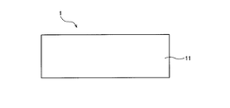
- FIG. 2 is a cross-sectional view showing a SiC substrate.
- the SiC substrate 11 is configured by forming a wafer layer made of SiC (not shown) and an epitaxial layer made of SiC on the wafer layer.
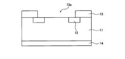
- FIG. 3 is a diagram illustrating a process of forming a guard ring.
- the guard ring 12 is formed by performing ion implantation on a part of the epitaxial layer on the front surface of the SiC substrate 11.
- FIG. 4 is a cross-sectional view showing a process of forming an insulating layer and a nickel silicide layer.
- An insulating layer 13 made of SiO 2 is formed on the guard ring 12. Thereafter, a layer containing nickel and titanium is formed on the back surface of SiC substrate 11, and nickel silicide layer 14 including titanium carbide is formed by subsequent heating.
- the layer containing nickel and titanium is preferably formed on the SiC substrate 11 in the order of nickel layer and titanium layer.
- the ratio between nickel and titanium can be achieved by forming a ratio of the respective film thicknesses from 1 to 1 to 10 to 1, preferably from 3 to 1 to 6 to 1, when nickel and titanium are formed in a laminate.
- the thickness of nickel is preferably 20 to 100 nm
- the thickness of titanium is preferably 10 to 50 nm.
- nickel may be formed as an alloy so that titanium is included.
- the ratio of nickel to titanium can be set to 1: 1 to 10: 1, preferably 3: 1 to 6: 1.
- the nickel silicide layer 14 is obtained by heating at 1000 to 1200 ° C. in an argon atmosphere.
- the formed nickel silicide layer 14 including titanium carbide has a thickness of 10 to 100 nm, preferably 20 to 30 nm.
- Titanium carbide has a function of suppressing peeling of the back electrode 18 in order to show good adhesion to titanium in the laminate constituting the back electrode 18 to be formed later. Further, in the nickel silicide layer including titanium carbide, when the number of carbon atoms contained in the titanium carbide on the outermost surface is 12% or more of the total number of carbon atoms deposited on the outermost surface, peeling from the back electrode 18 occurs. Since there is no, it is more preferable. In addition, even if it is less than 12%, peeling from the back surface electrode 18 can be suppressed and the yield can be improved.
- FIG. 5 is a cross-sectional view showing a process of forming a contact hole. As shown in FIG. 5, a part of the insulating layer 13 is removed by etching to form a contact hole 13a.
- FIG. 6 is a cross-sectional view showing a process of forming a Schottky electrode.
- a Schottky electrode 16 in contact with the SiC substrate 11 is formed in the contact hole 13a portion of the SiC substrate 11 exposed by etching.
- the Schottky electrode 16 for example, a titanium film is formed, and then a Schottky contact is formed by subsequent heating.
- the metal used for the Schottky electrode 16 may be tungsten, molybdenum, or chromium in addition to titanium.
- the heating temperature is about 400 to 600 ° C.
- the heating atmosphere is argon or helium. Under these heating conditions, part of the carbon contained in the nickel silicide layer 14 is deposited on the front surface (back side) of the nickel silicide layer 14 including titanium carbide, and the carbon layer 15 is formed as shown in FIG. It is formed.
- the carbon layer 15 is a several atomic layer and is deposited locally.
- FIG. 7 is a cross-sectional view showing the process of forming the surface electrode.
- the Schottky electrode 16 is covered with, for example, aluminum to form a surface electrode 17.
- Aluminum is formed by sputtering, for example, at a pressure of 0.2 Pa during sputtering and at a substrate temperature of 300 ° C. The pressure may be 0.1 Pa or more and 1 Pa or less, and the temperature of the SiC substrate 11 may be 100 ° C. or more and 500 ° C. or less.
- the same effect can be obtained by using aluminum containing silicon that is 0.1% or more and 10% or less instead of aluminum.
- FIG. 8 is a cross-sectional view showing the process of removing the carbon layer. As shown in FIG. 8, the carbon layer 15 formed on the surface of the nickel silicide layer 14 including titanium carbide (the back side of the SiC substrate 11) is removed.
- FIG. 9 is a cross-sectional view showing a step of forming a laminate of metal layers to form a back electrode. On the nickel silicide layer 14 containing titanium carbide from which the carbon layer 15 has been removed, a back electrode 18 made of a laminate in which titanium, nickel, and gold are laminated in this order is formed.
- the SiC substrate 11 on which all film forming operations have been completed can be diced to obtain a SiC Schottky barrier diode chip. Bonding is performed between the surface electrode pad of the obtained semiconductor chip and the lead frame and the conductor on the substrate by using an automatic wire bonding apparatus, and further molding is performed to obtain a discrete component.
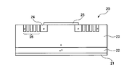
- FIG. 10 is a cross-sectional view illustrating a Schottky barrier diode (SBD) having a field limiting ring (FLR) structure according to an embodiment of the present invention.
- SBD Schottky barrier diode
- FLR field limiting ring
- an epitaxial layer (low concentration n type drift layer 23) is formed on a SiC substrate (high concentration n type substrate 22).
- An n-type region for a channel stopper, a p-type region (p-type impurity ion implantation region) 24 for a termination structure, and a p-type region 26 having a floating limiting ring (FLR) structure are formed on the SiC substrate 22 by ion implantation.
- phosphorus implanted to form the n-type region for the channel stopper and aluminum implanted to form the p-type region 24 for the termination structure and the p-type region 26 of the FLR structure are activated.
- activation was performed at 1620 ° C. for 180 seconds in an argon atmosphere.
- an SiO film having a thickness of 500 nm was formed on the surface side of the SiC substrate 22 using an atmospheric pressure CVD apparatus.
- a nickel layer with a thickness of 60 nm and a titanium layer with a thickness of 20 nm were stacked in this order from the substrate side on the back side of the SiC substrate 22 using a sputtering apparatus.
- the formed SiC substrate 22 was heat-treated at 1050 ° C. for 2 minutes in an argon atmosphere using a high-speed annealing apparatus (RTA) equipped with an infrared lamp. By this heat treatment, the silicon atoms of the SiC substrate 22 reacted with nickel to generate the nickel silicide layer 21, and an ohmic contact could be obtained.
- the nickel silicide layer 21 in FIG. 10 becomes an ohmic electrode.
- the carbon atoms of the SiC substrate 22 react with titanium to generate titanium carbide and deposit on the surface of the nickel silicide layer 21. At this time, unreacted carbon atoms remain in the nickel silicide layer 21, but the number of carbon atoms contained in the titanium carbide on the outermost surface of the nickel silicide layer 21 is 12% or more of the total number of carbon atoms deposited on the surface. Met.
- the number of carbon atoms was calculated by XPS analysis. The C1s peak observed around 283 eV was calculated from the total value of a plurality of C1s peak intensities appearing due to chemical shift and the peak intensity ratio derived from TiC.
- a contact hole is formed in the oxide film on the surface side using a hydrofluoric acid buffer solution (see FIG. 5 as a corresponding diagram), and a titanium film for Schottky electrode 25 is formed to 200 nm by a sputtering apparatus, and then an infrared lamp Was processed at 500 ° C. for 5 minutes in an argon atmosphere (see FIG. 6). At this time, carbon in the nickel silicide layer 21 was deposited, and a thin carbon layer was formed.
- aluminum for surface electrodes was quickly formed into a 5000 nm film using a sputtering apparatus (see FIG. 7).
- the pressure during sputtering is 0.2 Pa and the substrate temperature is 300 ° C.
- aluminum containing silicon that is 0.1% or more and 10% or less may be used instead of aluminum.
- the SiC substrate 22 is mounted in a vacuum pressure vessel having a substrate heating mechanism so that the back surface is exposed, and treated at 300 ° C. for 1 hour while introducing argon containing 1% oxygen or ozone.
- the carbon layer formed on the surface of the nickel silicide layer 21 was removed (see FIG. 8). Even if reverse sputtering is used, the same effect can be obtained.
- 70 nm of titanium, 700 nm of nickel, and 200 nm of gold were continuously vapor-deposited on the nickel silicide layer 21 using a vapor deposition apparatus to form a back electrode of the metal laminate (see FIG. 8).
- a nickel silicide layer (ohmic electrode) 21 and a back electrode made of a metal layer laminated on the ohmic electrode 21 form a back electrode structure of the FLR-SBD 20.
- FIG. 11 is a cross-sectional view illustrating a Schottky barrier diode (SBD) having a junction barrier Schottky (JBS) structure according to an embodiment of the present invention.
- SBD Schottky barrier diode
- JBS junction barrier Schottky
- FIG. 12 is a chart showing the relationship between the temperature and the reflectance when forming the surface electrode according to the present invention.
- FIGS. 13 and 14 are tables showing the relationship between the reflectance of the surface electrode in the SiC semiconductor device of the present invention and the recognition rate in the automatic wire bonding apparatus.
- FIG. 13 shows the number N of samples for each of a plurality of reflectance levels, and the number of recognitions and the recognition rates for different automatic wire bonding apparatuses A and B.
- the horizontal axis represents the reflectance (%)
- the vertical axis represents the recognition rate (%) for each of the automatic wire bonding apparatuses A and B.
- the recognition rate is 100% when the reflectance is 65% or less, and when another automatic wire bonding apparatus B is used, the reflectance is 55%.
- the recognition rate became 100% below.
- the recognition rate could be 100% with a reflectance of 55% or less.
- the reflectance is 50% or less, and the recognition rate can be 100%.
- a SiC semiconductor device As a comparison object for comparison with the above-described example, a SiC semiconductor device was manufactured in the same manner as the procedure of the manufacturing process. In the manufacturing process, the formation of the surface electrode was made different by forming aluminum at room temperature. With respect to the obtained SiC semiconductor device to be compared, a cross section of the surface electrode 17 was observed with a TEM. As a result, voids were found inside the surface electrode 17. That is, a portion where the surface electrode 17 is not densely coated with respect to the pattern irregularities of the Schottky electrode 16 occurs, and a SiC semiconductor device having a surface electrode structure composed of the Schottky electrode 16 and the surface electrode 17 with a poor quality is manufactured. It was. Further, the reflectance of the surface electrode 17 was 82%, and the surface electrode 17 could not be recognized by the automatic wire bonding apparatus.
- the surface electrode of the SiC semiconductor device of the present invention As described above, as is apparent from the results of the examples and comparative examples, according to the surface electrode of the SiC semiconductor device of the present invention, the coverage with respect to pattern irregularities is good, and this surface electrode is subjected to automatic wire bonding. Since it has the optimum reflectivity for image recognition when performing, it is possible to manufacture a SiC semiconductor device having excellent reliability. Further, since the reflectance of the surface electrode can be set to an optimum value, the yield when the manufactured SiC semiconductor device is mounted using an automatic wire bonding apparatus can be improved, and the productivity can be increased.
- the SiC semiconductor device according to the present invention is not limited to the Schottky barrier diode, and can be similarly applied to various semiconductor devices using SiC such as MOSFET. .
- the SiC semiconductor device of the present invention can be used as a high voltage, for example, a high breakdown voltage Schottky barrier diode of 1000 V or more, and the on-resistance can be lowered while suppressing leakage, so that the chip area is reduced and the unit price of the product Can be lowered.
- a diode having a large rated voltage can be manufactured, and can be applied to inverters such as industrial electric motors and Shinkansen vehicles that require a large current, thereby achieving high efficiency and downsizing of the apparatus.
- the semiconductor device manufacturing method according to the present invention is useful for power semiconductor devices such as power devices, and power semiconductor devices used for motor control and engine control for industrial or automobile use.
Landscapes
- Electrodes Of Semiconductors (AREA)
Abstract
Description
以下に添付図面を参照して、この発明にかかる半導体デバイスの製造方法の好適な実施の形態を詳細に説明する。本明細書および添付図面においては、nまたはpを冠記した層や領域では、それぞれ電子または正孔が多数キャリアであることを意味する。また、nやpに付す+および-は、それぞれそれが付されていない層や領域よりも高不純物濃度および低不純物濃度であることを意味する。
つぎに、図1~9に示した製造工程により製造したショットキーバリアダイオードの実施例について説明する。図10は、本発明の実施例によるフィールドリミッティングリング(FLR)構造を持つショットキーバリアダイオード(SBD)を示す断面図である。このFLR-SBD20の製造工程について説明する。
上記の実施例と対比するための比較対象として、上記製造工程の手順と同様に、SiC半導体デバイスを製造した。製造工程のうち、表面電極の形成については、アルミニウムを室温で形成して異ならせた。得られた比較対象のSiC半導体デバイスについて、表面電極17断面をTEM観察したところ、この表面電極17の内部に鬆(ボイド)が認められた。すなわち、ショットキー電極16のパターン凹凸に対して、表面電極17が密に被覆していない箇所が生じ、ショットキー電極16と表面電極17からなる表面電極構造が良質ではないSiC半導体デバイスが製造された。また、表面電極17の反射率は82%となり、自動ワイヤボンディング装置により表面電極17を認識することができなかった。
11 SiC基板
12 ガードリング
13 絶縁層
14 チタンカーバイドを包含したニッケルシリサイド層
15 炭素層
16 ショットキー電極
17 表面電極
18 裏面電極
21 オーミック電極
22 高濃度n型基板
23 低濃度n型ドリフト層
24 p型不純物イオン注入領域
25 ショットキー電極
26 FLR構造
27 JBS構造
Claims (4)
- 炭化珪素半導体基板に電極構造を形成する半導体デバイスの製造方法であって、
前記炭化珪素半導体基板のおもて面に、チタン、タングステン、モリブデン、クロムのいずれか一つの金属を含むショットキー層を形成し、
前記ショットキー層を加熱することにより、前記炭化珪素半導体基板とのショットキーコンタクトを有するショットキー電極を形成し、
アルミニウムまたは珪素を含むアルミニウムにより、前記ショットキー電極の表面に表面電極を形成するものであり、
前記表面電極の形成時には、当該表面電極が前記ショットキー電極の凹凸に対する被覆が良好で且つ前記表面電極が所定の反射率以下となる条件に適合した温度範囲を有して加熱することを特徴とする半導体デバイスの製造方法。 - 前記表面電極は、スパッタ法によって形成し、スパッタ中の圧力が0.1Pa以上1Pa以下であり、前記炭化珪素半導体基板の温度が100℃以上500℃以下であることを特徴とする請求項1に記載の半導体デバイスの製造方法。
- 前記表面電極の反射率が80%以下となる条件を有した温度範囲で加熱することを特徴とする請求項1に記載の半導体デバイスの製造方法。
- 前記炭化珪素半導体基板の裏面側に、チタンカーバイドを含むニッケルシリサイド層のオーミック電極と、金属層の裏面電極とからなる裏面電極構造を形成することを特徴とする請求項1~3のいずれか一つに記載の半導体デバイスの製造方法。
Priority Applications (4)
| Application Number | Priority Date | Filing Date | Title |
|---|---|---|---|
| CN201380018966.1A CN104272442B (zh) | 2012-04-18 | 2013-03-14 | 半导体器件的制造方法 |
| DE112013002109.9T DE112013002109T5 (de) | 2012-04-18 | 2013-03-14 | Verfahren zum Herstellen einer Halbleitervorrichtung |
| KR1020147028270A KR20140145588A (ko) | 2012-04-18 | 2013-03-14 | 반도체 디바이스의 제조 방법 |
| US14/511,151 US9263543B2 (en) | 2012-04-18 | 2014-10-09 | Method for manufacturing a semiconductor device |
Applications Claiming Priority (2)
| Application Number | Priority Date | Filing Date | Title |
|---|---|---|---|
| JP2012-095159 | 2012-04-18 | ||
| JP2012095159A JP5966556B2 (ja) | 2012-04-18 | 2012-04-18 | 半導体デバイスの製造方法 |
Related Child Applications (1)
| Application Number | Title | Priority Date | Filing Date |
|---|---|---|---|
| US14/511,151 Continuation US9263543B2 (en) | 2012-04-18 | 2014-10-09 | Method for manufacturing a semiconductor device |
Publications (1)
| Publication Number | Publication Date |
|---|---|
| WO2013157335A1 true WO2013157335A1 (ja) | 2013-10-24 |
Family
ID=49383303
Family Applications (1)
| Application Number | Title | Priority Date | Filing Date |
|---|---|---|---|
| PCT/JP2013/057312 Ceased WO2013157335A1 (ja) | 2012-04-18 | 2013-03-14 | 半導体デバイスの製造方法 |
Country Status (6)
| Country | Link |
|---|---|
| US (1) | US9263543B2 (ja) |
| JP (1) | JP5966556B2 (ja) |
| KR (1) | KR20140145588A (ja) |
| CN (1) | CN104272442B (ja) |
| DE (1) | DE112013002109T5 (ja) |
| WO (1) | WO2013157335A1 (ja) |
Cited By (1)
| Publication number | Priority date | Publication date | Assignee | Title |
|---|---|---|---|---|
| US20160254393A1 (en) * | 2013-11-22 | 2016-09-01 | Fuji Electric Co., Ltd. | Silicon carbide semiconductor device and method of manufacturing silicon carbide semiconductor device |
Families Citing this family (18)
| Publication number | Priority date | Publication date | Assignee | Title |
|---|---|---|---|---|
| JP6112699B2 (ja) * | 2012-03-30 | 2017-04-12 | 富士電機株式会社 | 炭化珪素半導体装置の製造方法及び該方法により製造された炭化珪素半導体装置 |
| JP6164062B2 (ja) * | 2013-11-22 | 2017-07-19 | 富士電機株式会社 | 炭化珪素半導体装置の製造方法 |
| US9552993B2 (en) * | 2014-02-27 | 2017-01-24 | Semiconductor Components Industries, Llc | Semiconductor device and manufacturing method thereof |
| WO2015166608A1 (ja) | 2014-04-30 | 2015-11-05 | 三菱電機株式会社 | 炭化珪素半導体装置 |
| DE102015102055A1 (de) * | 2015-01-16 | 2016-07-21 | Infineon Technologies Ag | Verfahren zum Bearbeiten einer Halbleiteroberfläche |
| CN107785250B (zh) * | 2016-08-31 | 2020-12-11 | 株洲中车时代半导体有限公司 | 碳化硅基肖特基接触制作方法及肖特基二极管制造方法 |
| JP6724685B2 (ja) * | 2016-09-23 | 2020-07-15 | 住友電気工業株式会社 | 半導体装置 |
| WO2018092129A1 (en) | 2016-11-15 | 2018-05-24 | The Medical Research,Infrastructure, And Health Services Fund Of The Tel-Aviv Medical Center | Tissue repair device and method |
| JP6922202B2 (ja) * | 2016-12-07 | 2021-08-18 | 富士電機株式会社 | 半導体装置および半導体装置の製造方法 |
| CN108321213A (zh) * | 2017-12-21 | 2018-07-24 | 秦皇岛京河科学技术研究院有限公司 | SiC功率二极管器件的制备方法及其结构 |
| JP7135443B2 (ja) * | 2018-05-29 | 2022-09-13 | 富士電機株式会社 | 炭化ケイ素半導体装置及びその製造方法 |
| JP7283053B2 (ja) * | 2018-11-09 | 2023-05-30 | 富士電機株式会社 | 炭化珪素半導体装置、炭化珪素半導体組立体および炭化珪素半導体装置の製造方法 |
| US12062698B2 (en) | 2019-08-01 | 2024-08-13 | Hitachi Energy Ltd | Silicon carbide transistor device |
| CN113745349A (zh) * | 2020-05-28 | 2021-12-03 | 世界先进积体电路股份有限公司 | 半导体装置 |
| JP7647146B2 (ja) * | 2021-02-17 | 2025-03-18 | 富士電機株式会社 | 炭化珪素半導体装置および炭化珪素半導体装置の製造方法 |
| CN113130624A (zh) * | 2021-03-26 | 2021-07-16 | 先之科半导体科技(东莞)有限公司 | 一种低损耗肖特基整流管及其成型工艺 |
| WO2023189055A1 (ja) * | 2022-03-31 | 2023-10-05 | ローム株式会社 | 半導体装置 |
| JP2024024452A (ja) * | 2022-08-09 | 2024-02-22 | 富士電機株式会社 | 炭化珪素半導体装置および炭化珪素半導体装置の製造方法 |
Citations (5)
| Publication number | Priority date | Publication date | Assignee | Title |
|---|---|---|---|---|
| JPH0284719A (ja) * | 1988-09-21 | 1990-03-26 | Nec Corp | 半導体装置の製造方法 |
| JPH0778786A (ja) * | 1993-09-07 | 1995-03-20 | Sony Corp | 半導体装置の配線構造の形成方法 |
| JP2006120761A (ja) * | 2004-10-20 | 2006-05-11 | Kansai Tlo Kk | 半導体装置製造方法 |
| JP2006344688A (ja) * | 2005-06-07 | 2006-12-21 | Denso Corp | 半導体装置およびその製造方法 |
| JP2009094392A (ja) * | 2007-10-11 | 2009-04-30 | Mitsubishi Electric Corp | 炭化珪素半導体装置の製造方法 |
Family Cites Families (8)
| Publication number | Priority date | Publication date | Assignee | Title |
|---|---|---|---|---|
| JP3871607B2 (ja) * | 2001-12-14 | 2007-01-24 | 松下電器産業株式会社 | 半導体素子およびその製造方法 |
| JP4501488B2 (ja) | 2004-03-26 | 2010-07-14 | 豊田合成株式会社 | 炭化珪素半導体のオーミック電極及びその製造方法 |
| US20070138482A1 (en) | 2005-12-08 | 2007-06-21 | Nissan Motor Co., Ltd. | Silicon carbide semiconductor device and method for producing the same |
| JP2007184571A (ja) | 2005-12-08 | 2007-07-19 | Nissan Motor Co Ltd | 炭化珪素半導体装置、炭化珪素半導体装置の製造方法、炭化珪素半導体装置中の遷移金属シリサイドと金属膜との接合体及び炭化珪素半導体装置中の遷移金属シリサイドと金属膜との接合体の製造方法 |
| JP2008135611A (ja) | 2006-11-29 | 2008-06-12 | Denso Corp | 半導体装置の製造方法 |
| JP4535151B2 (ja) * | 2008-03-19 | 2010-09-01 | 株式会社デンソー | 炭化珪素半導体装置の製造方法 |
| JP5369581B2 (ja) | 2008-09-29 | 2013-12-18 | 住友電気工業株式会社 | 半導体デバイス用裏面電極、半導体デバイスおよび半導体デバイス用裏面電極の製造方法 |
| JP5598015B2 (ja) * | 2010-02-23 | 2014-10-01 | 株式会社デンソー | ショットキーバリアダイオードを備えた炭化珪素半導体装置およびその製造方法 |
-
2012
- 2012-04-18 JP JP2012095159A patent/JP5966556B2/ja active Active
-
2013
- 2013-03-14 KR KR1020147028270A patent/KR20140145588A/ko not_active Withdrawn
- 2013-03-14 CN CN201380018966.1A patent/CN104272442B/zh active Active
- 2013-03-14 WO PCT/JP2013/057312 patent/WO2013157335A1/ja not_active Ceased
- 2013-03-14 DE DE112013002109.9T patent/DE112013002109T5/de not_active Withdrawn
-
2014
- 2014-10-09 US US14/511,151 patent/US9263543B2/en active Active
Patent Citations (5)
| Publication number | Priority date | Publication date | Assignee | Title |
|---|---|---|---|---|
| JPH0284719A (ja) * | 1988-09-21 | 1990-03-26 | Nec Corp | 半導体装置の製造方法 |
| JPH0778786A (ja) * | 1993-09-07 | 1995-03-20 | Sony Corp | 半導体装置の配線構造の形成方法 |
| JP2006120761A (ja) * | 2004-10-20 | 2006-05-11 | Kansai Tlo Kk | 半導体装置製造方法 |
| JP2006344688A (ja) * | 2005-06-07 | 2006-12-21 | Denso Corp | 半導体装置およびその製造方法 |
| JP2009094392A (ja) * | 2007-10-11 | 2009-04-30 | Mitsubishi Electric Corp | 炭化珪素半導体装置の製造方法 |
Cited By (2)
| Publication number | Priority date | Publication date | Assignee | Title |
|---|---|---|---|---|
| US20160254393A1 (en) * | 2013-11-22 | 2016-09-01 | Fuji Electric Co., Ltd. | Silicon carbide semiconductor device and method of manufacturing silicon carbide semiconductor device |
| US10600921B2 (en) * | 2013-11-22 | 2020-03-24 | Fuji Electric Co., Ltd. | Silicon carbide semiconductor device and method of manufacturing silicon carbide semiconductor device |
Also Published As
| Publication number | Publication date |
|---|---|
| US9263543B2 (en) | 2016-02-16 |
| JP2013222907A (ja) | 2013-10-28 |
| US20150024581A1 (en) | 2015-01-22 |
| DE112013002109T5 (de) | 2014-12-31 |
| JP5966556B2 (ja) | 2016-08-10 |
| CN104272442B (zh) | 2017-08-08 |
| CN104272442A (zh) | 2015-01-07 |
| KR20140145588A (ko) | 2014-12-23 |
Similar Documents
| Publication | Publication Date | Title |
|---|---|---|
| JP5966556B2 (ja) | 半導体デバイスの製造方法 | |
| JP6099298B2 (ja) | SiC半導体デバイス及びその製造方法 | |
| JP5525940B2 (ja) | 半導体装置および半導体装置の製造方法 | |
| JP5449786B2 (ja) | 炭化珪素半導体装置及び炭化珪素半導体装置の製造方法 | |
| US9240451B2 (en) | Silicon carbide semiconductor device | |
| US9159792B2 (en) | SiC semiconductor device and method for manufacturing the same | |
| JP6112699B2 (ja) | 炭化珪素半導体装置の製造方法及び該方法により製造された炭化珪素半導体装置 | |
| WO2012140794A1 (ja) | 炭化珪素半導体装置の製造方法 | |
| JP6051573B2 (ja) | 半導体装置の製造方法 | |
| JP6091703B2 (ja) | 炭化珪素半導体装置の製造方法及び炭化珪素半導体装置 | |
| JP4091931B2 (ja) | SiC半導体装置およびSiC半導体装置の製造方法 | |
| JP4087365B2 (ja) | SiC半導体装置の製造方法 | |
| JP2018049927A (ja) | 炭化珪素半導体装置およびその製造方法 | |
| JP5991629B2 (ja) | 半導体装置および半導体装置の製造方法 | |
| JP2016174070A (ja) | ショットキーバリアダイオードおよびその製造方法 | |
| JP2017168679A (ja) | 炭化珪素半導体素子および炭化珪素半導体素子の製造方法 | |
| JP2019140234A (ja) | 半導体装置 | |
| CN117438296A (zh) | 碳化硅半导体衬底上制造接触的方法和碳化硅半导体器件 | |
| JP2016086131A (ja) | 炭化珪素半導体装置の製造方法 |
Legal Events
| Date | Code | Title | Description |
|---|---|---|---|
| 121 | Ep: the epo has been informed by wipo that ep was designated in this application |
Ref document number: 13778659 Country of ref document: EP Kind code of ref document: A1 |
|
| ENP | Entry into the national phase |
Ref document number: 20147028270 Country of ref document: KR Kind code of ref document: A |
|
| WWE | Wipo information: entry into national phase |
Ref document number: 112013002109 Country of ref document: DE Ref document number: 1120130021099 Country of ref document: DE |
|
| 122 | Ep: pct application non-entry in european phase |
Ref document number: 13778659 Country of ref document: EP Kind code of ref document: A1 |