WO2013153786A1 - Dispositif de stockage non volatil et procédé pour sa formation - Google Patents
Dispositif de stockage non volatil et procédé pour sa formation Download PDFInfo
- Publication number
- WO2013153786A1 WO2013153786A1 PCT/JP2013/002339 JP2013002339W WO2013153786A1 WO 2013153786 A1 WO2013153786 A1 WO 2013153786A1 JP 2013002339 W JP2013002339 W JP 2013002339W WO 2013153786 A1 WO2013153786 A1 WO 2013153786A1
- Authority
- WO
- WIPO (PCT)
- Prior art keywords
- resistance value
- memory cell
- value information
- voltage
- read
- Prior art date
Links
Images


Classifications
-
- G—PHYSICS
- G11—INFORMATION STORAGE
- G11C—STATIC STORES
- G11C13/00—Digital stores characterised by the use of storage elements not covered by groups G11C11/00, G11C23/00, or G11C25/00
- G11C13/0002—Digital stores characterised by the use of storage elements not covered by groups G11C11/00, G11C23/00, or G11C25/00 using resistive RAM [RRAM] elements
- G11C13/0007—Digital stores characterised by the use of storage elements not covered by groups G11C11/00, G11C23/00, or G11C25/00 using resistive RAM [RRAM] elements comprising metal oxide memory material, e.g. perovskites
-
- G—PHYSICS
- G11—INFORMATION STORAGE
- G11C—STATIC STORES
- G11C11/00—Digital stores characterised by the use of particular electric or magnetic storage elements; Storage elements therefor
- G11C11/56—Digital stores characterised by the use of particular electric or magnetic storage elements; Storage elements therefor using storage elements with more than two stable states represented by steps, e.g. of voltage, current, phase, frequency
- G11C11/5685—Digital stores characterised by the use of particular electric or magnetic storage elements; Storage elements therefor using storage elements with more than two stable states represented by steps, e.g. of voltage, current, phase, frequency using storage elements comprising metal oxide memory material, e.g. perovskites
-
- G—PHYSICS
- G11—INFORMATION STORAGE
- G11C—STATIC STORES
- G11C13/00—Digital stores characterised by the use of storage elements not covered by groups G11C11/00, G11C23/00, or G11C25/00
- G11C13/0002—Digital stores characterised by the use of storage elements not covered by groups G11C11/00, G11C23/00, or G11C25/00 using resistive RAM [RRAM] elements
- G11C13/0021—Auxiliary circuits
- G11C13/0038—Power supply circuits
-
- G—PHYSICS
- G11—INFORMATION STORAGE
- G11C—STATIC STORES
- G11C13/00—Digital stores characterised by the use of storage elements not covered by groups G11C11/00, G11C23/00, or G11C25/00
- G11C13/0002—Digital stores characterised by the use of storage elements not covered by groups G11C11/00, G11C23/00, or G11C25/00 using resistive RAM [RRAM] elements
- G11C13/0021—Auxiliary circuits
- G11C13/0064—Verifying circuits or methods
-
- G—PHYSICS
- G11—INFORMATION STORAGE
- G11C—STATIC STORES
- G11C13/00—Digital stores characterised by the use of storage elements not covered by groups G11C11/00, G11C23/00, or G11C25/00
- G11C13/0002—Digital stores characterised by the use of storage elements not covered by groups G11C11/00, G11C23/00, or G11C25/00 using resistive RAM [RRAM] elements
- G11C13/0021—Auxiliary circuits
- G11C13/0069—Writing or programming circuits or methods
-
- G—PHYSICS
- G11—INFORMATION STORAGE
- G11C—STATIC STORES
- G11C11/00—Digital stores characterised by the use of particular electric or magnetic storage elements; Storage elements therefor
- G11C11/02—Digital stores characterised by the use of particular electric or magnetic storage elements; Storage elements therefor using magnetic elements
- G11C11/16—Digital stores characterised by the use of particular electric or magnetic storage elements; Storage elements therefor using magnetic elements using elements in which the storage effect is based on magnetic spin effect
-
- G—PHYSICS
- G11—INFORMATION STORAGE
- G11C—STATIC STORES
- G11C13/00—Digital stores characterised by the use of storage elements not covered by groups G11C11/00, G11C23/00, or G11C25/00
- G11C13/0002—Digital stores characterised by the use of storage elements not covered by groups G11C11/00, G11C23/00, or G11C25/00 using resistive RAM [RRAM] elements
- G11C13/0021—Auxiliary circuits
- G11C13/0069—Writing or programming circuits or methods
- G11C2013/0083—Write to perform initialising, forming process, electro forming or conditioning
-
- G—PHYSICS
- G11—INFORMATION STORAGE
- G11C—STATIC STORES
- G11C2213/00—Indexing scheme relating to G11C13/00 for features not covered by this group
- G11C2213/30—Resistive cell, memory material aspects
- G11C2213/32—Material having simple binary metal oxide structure
-
- G—PHYSICS
- G11—INFORMATION STORAGE
- G11C—STATIC STORES
- G11C2213/00—Indexing scheme relating to G11C13/00 for features not covered by this group
- G11C2213/70—Resistive array aspects
- G11C2213/72—Array wherein the access device being a diode
Definitions
- the present invention relates to a nonvolatile memory device that stores information using a nonvolatile resistance change element and a forming method thereof, and more particularly to a forming process for reversibly changing a resistance change element based on an electric pulse. .
- Nonvolatile memory devices are widely installed in mobile devices such as mobile phones and digital cameras, and their use is rapidly expanding.
- variable resistance element has a property that the resistance value reversibly changes to a level of at least two values or more according to an electrical signal, and further, information corresponding to the resistance value can be stored in a nonvolatile manner.
- a possible element is a property that the resistance value reversibly changes to a level of at least two values or more according to an electrical signal, and further, information corresponding to the resistance value can be stored in a nonvolatile manner.
- a memory cell array is formed by connecting a memory cell in which a resistance change element and a current control element (for example, a diode) are connected in series to a word line (row selection line) and a bit line (column selection line).
- a cross-point type nonvolatile memory device (hereinafter also referred to as “cross-point type nonvolatile memory”) has been proposed.
- JP 2010-218603 A JP 2011-66363 A JP 2011-198445 A Japanese Patent Laid-Open No. 2005-3401
- a process (formation process) for applying a forming voltage larger than that during normal operation to the resistance change element is performed in advance, and the resistance change element is set to a predetermined value.
- the resistance must be reduced to the level of.
- an object of the present invention is to provide a nonvolatile memory device that performs stable and accurate forming processing on a resistance change element, and that can stably change resistance after the forming processing.
- a nonvolatile memory device reversibly changes a resistance change element based on an electric pulse by applying a forming voltage to a memory cell including the resistance change element.
- a non-volatile memory device in which resistance change is possible wherein the memory cell, a voltage applying unit that applies a forming voltage to the memory cell, a reading unit that reads resistance value information of the memory cell, and the memory Before the forming voltage is applied to the cell, a storage unit that stores the resistance value information read from the memory cell by the reading unit as initial resistance value information, and resistance value information of the memory cell that the reading unit reads.
- the voltage application unit applies a forming voltage to the memory cell.
- the reading unit is characterized in that it comprises a control unit for controlling so as to repeat the step of reading the resistance value information of the memory cell.
- a system may be realized by a system, a method, an integrated circuit, a computer program, or a recording medium, and may be any combination of the system, method, integrated circuit, computer program, and recording medium. It may be realized. For example, more specifically, a desired operation may be performed by a nonvolatile memory device, an inspection device connected to the nonvolatile memory device, and a program that controls them.
- nonvolatile memory device that can perform a stable and appropriate forming process on the variable resistance element and can stably change the resistance after the forming process.
- FIG. 1 is a block diagram of the nonvolatile memory device according to this embodiment.
- FIG. 2 is an explanatory diagram illustrating an example of a cross-sectional configuration of the memory cell of the present embodiment.
- FIG. 3 is a block diagram when the configuration of a conventional readout circuit is used in this embodiment.
- FIG. 4 is an explanatory diagram for explaining a first problem when a conventional readout circuit is used.
- FIG. 5 is an explanatory diagram for explaining a second problem when a conventional readout circuit is used.
- FIG. 6 is a block diagram illustrating a configuration of the first readout circuit of the present embodiment.
- FIG. 7 is an explanatory diagram for explaining the improvement effect by the readout circuit of the present embodiment.
- FIG. 1 is a block diagram of the nonvolatile memory device according to this embodiment.
- FIG. 2 is an explanatory diagram illustrating an example of a cross-sectional configuration of the memory cell of the present embodiment.
- FIG. 3 is a block diagram when the configuration of
- FIG. 8 is a block diagram illustrating a configuration of the second readout circuit of the present embodiment.
- FIG. 9 is a timing chart for explaining the operation of the second readout circuit of this embodiment.
- FIG. 10 is a flowchart of the operation of the second readout circuit of this embodiment.
- FIG. 11 is a graph showing the relationship between the count value read as resistance value information by the second readout circuit of the present embodiment and the normalized cell current value.
- Nonvolatile memory devices also referred to as nonvolatile memory devices
- portable devices such as mobile phones and digital cameras
- their use is rapidly expanding.
- opportunities for handling audio data and image data are increasing, and therefore, there is a strong demand for a nonvolatile memory device that has a larger capacity and operates at a higher speed than before.
- nonvolatile storage device since such a nonvolatile storage device is often used for applications such as portable devices, low power consumption is required.
- cross-point type nonvolatile memory (hereinafter also referred to as “cross-point type nonvolatile memory”) that forms a memory cell array has been proposed.
- the cross-point type nonvolatile memory since a selection element such as a switching transistor is omitted, it is not necessary to form a selection element and its control wiring. Accordingly, the cross-point type nonvolatile memory is suitable for increasing the capacity because the memory array can be integrated at a high density based on the wiring rule of the minimum pitch.
- Cross point type especially ReRAM (Resistive RAM), which changes resistance at high speed with electrical pulses, has a simple structure in which a resistance change film is sandwiched between electrodes. It is expected that a high-density nonvolatile memory device can be realized. Further, the ReRAM disclosed in Patent Document 1 has been proposed that includes a memory cell array having a three-dimensional structure in which a plurality of cross-point type nonvolatile memory arrays are stacked on a substrate. It is stated that this has the advantage that the chip area can be significantly reduced for the same capacitance.
- the resistance change film used for ReRAM is an oxide of a transition metal, and a region in which the resistivity is locally reduced (hereinafter referred to as “filament path” as appropriate) is generated in the oxide film. It is stated that the resistance change is caused by the formation or decomposition of the filament path. Furthermore, the variable resistance element is in an insulating state in an initial state after manufacture, and in order to switch between a high resistance state (also referred to as an HR state) and a low resistance state (also referred to as an LR state) by electrical stress, First, it is extended that it is necessary to apply a voltage to a memory cell immediately after manufacture to form a filament path in the variable resistance element. The process of forming a filament path in the variable resistance element is called a forming process (hereinafter also simply referred to as forming).
- Patent Document 1 exemplifies that a desired resistance change cannot be performed unless the resistance can be lowered to a predetermined low resistance level by the forming process. For this reason, the resistance value is measured and measured after the voltage is applied. It is disclosed that voltage application and resistance measurement are repeated until the resistance value falls within a predetermined range. It is also described that there are a plurality of levels of applied voltages used for at least the forming process and that the applied pulse width is variable.
- Patent Document 2 discloses shortening the forming time by forming a plurality of elements in parallel and limiting the voltage application for each cell that has been formed.
- the cross-point type nonvolatile memory has an array structure in which memory cells including variable resistance elements are arranged at intersections of a plurality of first wirings and a plurality of second wirings.
- a forming voltage is applied to form a selected memory cell between the selected first wiring and the second wiring, a leakage current flows through the unselected first wiring and the second wiring. It is shown.
- This leakage current increases with time, and the forming voltage applied to the selection element gradually decreases. For this reason, the leakage current is detected, and the drive current of the driver applying the forming voltage is compensated according to the amount of leakage current to prevent the voltage drop.
- the same forming voltage is always applied to the variable resistance element regardless of the magnitude of the leakage current. It is shown to be applied.
- the present invention has been found for the purpose of providing a nonvolatile memory device capable of performing a stable and accurate forming process on a variable resistance element and capable of stably changing the resistance after the forming process.
- a nonvolatile memory device is a nonvolatile memory device in which a resistance voltage is reversibly changed based on an electric pulse by applying a forming voltage to a memory cell having a resistance change element.
- a memory storage device a voltage application unit that applies a forming voltage to the memory cell; a read unit that reads resistance value information of the memory cell; and the forming voltage applied to the memory cell.
- the storage unit stores the resistance value information read from the memory cell by the reading unit as initial resistance value information before, and the resistance value information of the memory cell read by the reading unit is based on the initial resistance value information.
- the voltage application unit applies a forming voltage to the memory cell until the set condition is satisfied, and the reading Characterized in that is part and a control unit that controls so as to repeat the step of reading the resistance value information of the memory cell.
- the memory array immediately before forming is performed for each memory cell.
- the threshold value automatically follows optimally and appropriate forming can be executed.
- control unit applies the forming voltage to the memory cell until the resistance value represented by the resistance value information of the memory cell becomes lower than the resistance value represented by the initial resistance value information.
- the reading unit may be controlled to repeat the step of reading the resistance value information of the memory cell.
- the control unit further includes a calculation unit that outputs calculation resistance value information obtained by multiplying the initial resistance value information by a predetermined coefficient, and the control unit has a resistance value represented by the resistance value information of the memory cell read by the reading unit.
- the voltage application unit repeats the step of applying a forming voltage to the memory cell and the reading unit reads the resistance value information of the memory cell until the resistance value is lower than the resistance value represented by the calculated resistance value information. You may control as follows.
- the read unit counts a discharge time until a voltage at both ends of the memory cell decreases to a predetermined reference voltage after a predetermined read voltage is applied to both ends of the memory cell at a predetermined cycle.
- the counter circuit reads a count value as the resistance value information
- the storage unit is a latch circuit that stores initial resistance value information read from the memory cell by the counter circuit before the memory cell is formed.
- the calculation unit may be a digital calculation circuit that outputs calculation resistance value information obtained by multiplying the initial resistance value information by a predetermined coefficient.
- the control unit further includes a constant current driving circuit for supplying a predetermined current to the memory cell based on the control of the control unit, and the control unit increases the discharge time by the predetermined current to obtain the resistance value information.
- the voltage application unit applies a forming voltage to the memory cell until the resistance value represented by the corrected resistance value information is lower than the resistance value represented by the calculated resistance value information; and the read unit May be controlled to repeat the step of reading the resistance value information of the memory cell.
- the resolution of the resistance value information can be ensured by extending the discharge time with the constant current source.
- control unit decreases the predetermined reference voltage and increases the predetermined current as the resistance value represented by the resistance value information read by the counter circuit decreases.
- the resistance value information may be corrected by increasing the predetermined read voltage.
- the resolution of the resistance value information can be freely set by adjusting the predetermined current amount of the constant current source, the clock frequency, the voltage of the reference voltage, and the capacitance of the capacitive element.
- the reading unit includes a capacitor connected in parallel with the memory cell, and the control unit has a resistance value represented by the resistance value information acquired by the counter circuit while the application of the forming voltage is repeated. As the voltage decreases, the resistance value information may be corrected by increasing the capacitance.
- control unit may perform control to lower the forming voltage as the resistance value indicated by the resistance value information read by the reading unit decreases while the application of the forming voltage is repeated.
- control unit may perform control to reduce the pulse width of the forming voltage as the resistance value indicated by the resistance value information read by the reading unit decreases while the application of the forming voltage is repeated.
- the readout unit includes a fixed resistor connected in series to the memory cell, and a capacitor that is connected in parallel to the fixed resistor and functions as the storage unit by storing a potential of the fixed resistor.
- the read unit may read a potential of the fixed resistor generated by a current flowing through the fixed resistor from the memory cell as the resistance value information after a predetermined read voltage is applied to both ends of the memory cell.
- the nonvolatile memory device includes a memory cell array including a plurality of memory cells including the memory cell, and the read unit receives the next memory after the resistance value information of the memory cell satisfies the condition.
- the cell resistance value information may be read, and the storage unit may store an initial resistance value of the next memory cell.
- control unit uses the calculated resistance value information obtained by multiplying the initial resistance value information by a predetermined coefficient as a first threshold value, and at least two threshold values including a second threshold value smaller than the first threshold value.
- the predetermined value is set to be larger than the second threshold value.
- the resistance value information may be corrected by decreasing a reference voltage, increasing the predetermined current, or increasing the predetermined read voltage.
- the forming method of the nonvolatile memory device can reversibly change the resistance of the variable resistance element based on an electric pulse by applying a forming voltage to the memory cell including the variable resistance element.
- a non-volatile storage device forming method comprising: storing resistance value information read from the memory cell as initial resistance value information; and storing the initial resistance value information, A step of applying the forming voltage to the memory cell; a step of reading resistance value information from the memory cell after the forming voltage is applied to the memory cell; and the resistance value information read in the reading step.
- the nonvolatile memory device includes a memory cell array including a plurality of memory cells including the memory cell, and if the condition is satisfied as a result of the determination step, You may perform the step which memorize
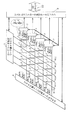
- FIG. 1 shows a block diagram of a nonvolatile memory device according to this embodiment.
- the memory cell 1 and the memory cell 2 are crossings in which word lines WL1 to WL5 and bit lines BL10 to BL1e, BL20 to BL2e, BL30 to BL3e, and BL40 to BL4e are arranged in a lattice pattern.
- word lines WL1 to WL5 and bit lines BL10 to BL1e, BL20 to BL2e, BL30 to BL3e, and BL40 to BL4e are arranged in a lattice pattern.
- BL40 to BL4e are arranged in a lattice pattern.
- memory cells are shown only at the intersections of WL1, WL2, WL3, WL4, and WL5 and BL10, BL20, BL30, and BL40, and the others are omitted.
- the memory cell 1 and the memory cell 2 include a resistance change element 5 and a bidirectional current control element 6 (for example, a bidirectional diode).
- the row decoder and the word line driver 3 (voltage application unit; hereinafter also referred to as the word line driver 3 as appropriate) are connected to the word line in accordance with instructions from the system controller and data buffer 9 (control unit; hereinafter also referred to as the system controller 9 as appropriate). Is set to a predetermined voltage or high impedance (HiZ).
- the column decoder and the bit line driver 4 (hereinafter also referred to as the bit line driver 4 as appropriate) set the voltage applied to the bit line to a predetermined voltage or set it to high impedance (HiZ) according to an instruction from the system controller 9. Set.
- the read circuit 7 selects a bit line based on designation from the system controller 9 among a plurality of bit lines, measures the potential state of the selected bit line and the amount of current flowing, and obtains information based on the resistance value of the resistance change element. Output to the system controller.
- the host interface 10 communicates data and control commands between the nonvolatile memory device according to the present embodiment and an external device.
- the system controller and data buffer 9 appropriately controls the word line driver 3 and the bit line driver 4 in accordance with commands and data from the host interface 10 to write data to the memory array and to read data from the memory array. Read out.
- system controller 9 when the system controller 9 receives a command in the read mode from the host interface 10, information based on the desired resistance value of the selected memory cell is input to the system controller 9 by the read circuit 7. The system controller 9 restores the original digital data and outputs the data through the host interface 10.
- FIG. 1 shows a memory array having five word lines, it is not limited to this number and aspect ratio. There is no problem even if the vertical relationship between the bit lines and the word lines and the connection relationship between the read circuit and each driver are switched.
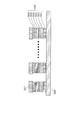
- FIG. 2 is a diagram showing a cross-sectional structure of the memory array according to the first embodiment.
- FIG. 2 shows a cross-sectional structure when the memory array is cut in a cross section in the bit line direction, and therefore the lower wiring 508 is a bit line.
- the upper wiring 507 is each word line, and a memory cell 500 is formed at the intersection of the bit line and the word line.
- the memory cell 500 includes a resistance change element and a bidirectional current control element.
- the memory cell 500 shown in FIG. 2 is formed by a semiconductor process structure including a general transistor, and is configured using, for example, a plug layer on a semiconductor substrate.
- the memory cell 500 includes a first electrode layer 501 that is a first electrode formed on the lower wiring 508, a bidirectional current control element 502, an intermediate electrode layer 503, an intermediate electrode layer 503, and a second electrode layer 506. Resistance change layers 504 and 505 sandwiched between the layers.
- the resistance change layer 504 is a first oxide layer, for example, a first tantalum-containing layer with a low oxygen content.
- the resistance change layer 505 is a second oxide layer, for example, a second tantalum-containing layer having a high oxygen content formed on the first tantalum-containing layer.
- the relationship between the thicknesses of the layers and the vertical relationship between the resistance change layer and the bidirectional current control element are not limited to the configuration shown in the figure, and are appropriately changed to an optimal arrangement and shape according to the semiconductor process.
- the order of layer arrangement of the variable resistance element structure may be changed.
- an adhesion layer or the like may be inserted between layers, or a predetermined material may be doped.
- Examples of the material of the first electrode layer 501, the intermediate electrode layer 503, and the second electrode layer 506 include Pt (platinum), Ir (iridium), W (tungsten), Cu (copper), Al (aluminum), TiN ( Titanium nitride), TaN (tantalum nitride), TiAlN (titanium aluminum nitride) and the like are used.
- an oxygen-deficient transition metal oxide preferably an oxygen-deficient Ta oxide
- An oxygen-deficient transition metal oxide is an oxide having a lower oxygen content (atomic ratio: ratio of the number of oxygen atoms to the total number of atoms) than an oxide having a stoichiometric composition. .
- the transition metal element is tantalum (Ta)
- the stoichiometric oxide composition is Ta 2 O 5 and the ratio of the number of atoms of Ta and O (O / Ta) is 2.5. is there. Therefore, in the oxygen-deficient Ta oxide, the atomic ratio of Ta and O is larger than 0 and smaller than 2.5.
- the transition metal element include Fe (iron), Zn (zinc), Cr (chromium), Ni (nickel), Ti (titanium), W, and Hf (hafnium).
- the oxygen-deficient transition metal oxide is preferably an oxygen-deficient Ta oxide.
- the resistance change layer 504 is a first tantalum-containing layer having a composition represented by TaO x (where 0 ⁇ x ⁇ 2.5), and the resistance change layer 504 is TaO y (where a second tantalum-containing layer having a composition represented by x ⁇ y ⁇ 2.5), and these two layers form a laminated structure.
- a third tantalum-containing layer and other transition metal oxide layers may be appropriately disposed, and a small amount of impurities may be doped in the two layers.
- TaO x as the first tantalum-containing layer preferably satisfies 0.8 ⁇ x ⁇ 1.9
- TaO y preferably satisfies x ⁇ y.
- the thickness of the first tantalum-containing layer is preferably 5 nm to 30 nm, whereas the thickness of the second tantalum-containing layer is preferably 1 nm to 8 nm, and the thickness of the second tantalum-containing layer is the first tantalum-containing layer. Thinner is preferred.
- a predetermined second voltage is applied in a direction in which current flows from the second electrode layer 506 in contact with the resistance change layer 505 to the intermediate electrode layer 503 in contact with the resistance change layer 504.
- HR state a high resistance state
- first resistance state a resistance value lower than that of the second resistance state.
- Transition to a low resistance state referred to as LR state or LR. That is, the direction of resistance change is determined by the way in which the second oxide layer having a high oxygen content is in contact with the electrode.
- the memory cell when a predetermined second voltage is applied in the direction in which current flows from the upper electrode to the lower electrode from the structure of the variable resistance element, the memory cell is brought into a high resistance state. Change. Conversely, when a predetermined first voltage is applied in the direction in which current flows from the lower electrode to the upper electrode, the memory cell changes to a low resistance state.
- the system controller 9 applies all the bit line and word line potentials to the intermediate precharge voltage Vpr, and then the word line WL1. Is set to a potential of VwHa larger than the Vpr voltage. At the same time, the system controller 9 sets the potentials of the bit lines BL10, BL20, BL30, and BL40 to VwHb smaller than the Vpr voltage, and the other non-selected word lines and bit lines have high impedance (hereinafter referred to as HiZ). Terminate. At this time, since the difference between VwHa and VwHb is equal to or higher than the second voltage, the memory cell is in a high resistance state. That is, 1 of digital data can be written in the memory cell.
- the system controller 9 when writing 0 of digital data, applies the potentials of all the bit lines and the word lines to the intermediate precharge voltage Vpr, and then the potential of the word line WL1 is smaller than the Vpr voltage. The potential is set to VwLb. At the same time, the system controller 9 sets the potentials of the bit lines BL10, BL20, BL30, and BL40 to VwLa larger than the Vpr voltage, and the other non-selected word lines and bit lines are terminated with high impedance (hereinafter referred to as HiZ). . At this time, since the difference between VwLa and VwLb is equal to or higher than the first voltage, the memory cell is in a low resistance state. That is, 0 of digital data can be written in the memory cell.
- HiZ high impedance
- FIG. 3 shows a circuit of the readout circuit 7.
- the readout circuit in FIG. 3 is a general circuit example shown in Patent Document 4 and is referred to as a conventional readout circuit 7 in order to distinguish it from the readout circuit according to the present embodiment.
- TR10 to TR1e and TR20 to TR2e are transistors.
- NWR is at a low level
- TR10 to TR1e are all turned off, and the read circuit 7 is disconnected from the bit lines of the memory array.
- NWR is at a high level
- all of TR10 to TR1e are turned on, and the read circuit 7 is connected to the bit line of the memory array.
- one of the control lines Y10 to Y1e becomes high level, and one of TR20 to TR2e is turned on.
- one of the bit lines BL10 to BL1e is input to the comparator CP1. Therefore, the voltage VRR across the fixed resistor RR changes according to the amount of current flowing through the selected bit line.
- This VRR becomes the amount of information based on the resistance value of the memory cell, and the comparator CP1 compares the threshold voltage of Vref1, outputs 1 (high level) to Dout as a low resistance state if it is larger than Vref1, and increases if it is smaller than Vref1. As a resistance state, 0 (low level) is output to Dout.
- the current flowing through the selected memory cell is input to the read circuit and appears as the potential across the fixed resistor RR of each conventional read circuit 7 as the amount of information based on the resistance value of the selected memory cell, and the data stored in the selected memory cell Is read out.
- the resistance change element using the tantalum oxide exemplified in this embodiment is in an insulating state in an initial state after manufacture. Therefore, in order to make the resistance change element switchable between a high resistance state and a low resistance state by electrical stress, a predetermined voltage is applied in advance to the resistance change element to form a filament path in the resistance change element. A forming process is required. Since the number of application times at which forming is achieved due to variations in the same array differs for each target cell (resistance change element), it is determined whether or not the forming process has been completed as already described using Patent Document 1. Specifically, after the forming voltage is applied, the resistance value information of the target cell is read, and the application and reading of the resistance value information are repeated until a predetermined low resistance state is reached.
- VFref voltage that is a threshold value at the time of forming is input to the Vrefin terminal in FIG. 3, and if the VRR voltage becomes higher than the VFref voltage and lower than a predetermined resistance value of the memory cell, it is determined that the forming process is completed, Move to the next address cell. Then, when the forming process of the memory cells of all target addresses is completed, the process ends.
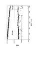
- FIG. 4 shows the change in the resistance value of the memory cell at each address when the VRR 300k voltage is applied to the Vrefin terminal and the first forming process example is performed.
- the horizontal axis represents the relative address of the memory cell
- the vertical axis represents the resistance value of the memory cell.
- x indicates the initial resistance value immediately before starting the forming process of each memory cell
- ⁇ indicates the resistance value of each memory cell immediately after the forming process is completed exceeding the threshold value.
- Each resistance value is obtained by measuring the VRR voltage by a general tester device separately from the readout circuit 7.
- the initial resistance of all memory cells is about 10 M ⁇ .
- the initial resistance value immediately before each memory cell decreases as the number of cells in which the forming process is completed increases. This is because the resistance change element, which was an insulator, is turned on by the forming process, so that the leakage current of the memory array gradually increases, and the apparent resistance value is observed to be low.
- the state after forming differs for each memory cell depending on the magnitude of the leakage current. It can be seen that the memory cells plotted in the portion surrounded by the broken line in FIG. 4 have extremely low resistance. This is because the diode of the selection element is broken and is in a state close to a short circuit.
- the memory cell at each address is rewritten.
- the change in the resistance value is shown in FIG.
- the relationship between the vertical axis and the horizontal axis in FIG. 5 is the same as in FIG. 4, where ⁇ marks indicate the HR state of each memory cell, and black square marks indicate the LR state.
- ⁇ marks indicate the HR state of each memory cell
- black square marks indicate the LR state.
- the first half region with little leakage current is strongly formed and the resistance value level is low, whereas the second half region is weakly formed and the resistance value level is high.
- the latter half region where only weak forming is performed there are some malfunctioning cells that cannot change resistance to the LR state as indicated by arrows.
- the leakage current increases depending on the number of memory cells that have undergone the forming process, it is understood that normal forming cannot be performed if the forming threshold is fixed to one type.
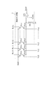
- FIG. 6 is a first read circuit example according to the present embodiment.
- the parts other than the read circuit that is, the memory cell, the system controller 9 (control unit), the word line driver 3 (voltage application unit), and the bit line driver 4 are shown in FIGS.
- the first readout circuit 7a will be described.
- a resistance value information hold circuit 20a is newly added to the configuration of FIG.
- the resistance value information hold circuit 20a includes SW1, SW2, a capacitor CC, and amp1.
- SW1 is turned on when the signal RE is “H” and turned off when the signal RE is “L”.
- SW2 is turned on when the signal Rhold is “H” and turned off when the signal Rhold is “L”.
- the capacitor CC (storage unit) is a capacitor having a predetermined capacity, and, for example, a MOS capacitor is used in the semiconductor process.
- Amp1 (arithmetic unit) is an amplifier that amplifies an input voltage to n / m (n> m) and outputs the amplified voltage.
- the amplification ratio of amp1 can be changed by setting from the Gain terminal.
- “L” is input to Rhold
- “H” is input to RE
- SW2 is turned OFF
- SW1 is turned ON
- the input voltage from Vrefin is input to CP1 as a threshold voltage via amp1. Is done.
- a memory cell to be formed is selected, and initial resistance value information of the selected memory cell is acquired before a forming voltage is applied.
- the RE terminal is set to low level
- SW1 is off
- the selected cell is set to the read state
- the read voltage is generated at both ends of the fixed resistor RR (read unit)
- the Rhold terminal is set to low level ⁇ high level ⁇ low.
- the level is changed and SW2 is turned off ⁇ on ⁇ off.
- the resistance value information is a voltage charged in the capacitor CC
- the capacitor CC is the resistance value information (the fixed resistor RR) read from the memory cell by the reading unit (fixed resistor RR).
- the potential at both ends) is stored as initial resistance value information.
- a predetermined time is required for charging the capacitor CC, and the above-described period in which SW2 is on is sufficiently longer than the time required for charging. That is, the information amount based on the initial resistance of the selected memory cell is held in the voltage across the capacitor CC. Then, the completion of forming is determined using a voltage obtained by multiplying the voltage by n / m as a threshold value. The charge charged in the capacitor CC is discharged little by little, but it is designed to maintain a desired level until the forming is completed.
- the forming method is the same as described in FIG. That is, instead of using the absolute resistance value as a threshold value, it is determined that the forming is completed using the resistance value information obtained by multiplying the initial resistance value information measured for each cell by a predetermined ratio by amp1 as a threshold value. To work. That is, the system controller 9 (control unit) waits until the resistance value indicated by the resistance value information of the memory cell read by the read circuit 7a is lower than the resistance value based on the initial resistance value information. ) Is controlled to repeat the application of the forming voltage.
- the threshold value is obtained by multiplying the initial resistance value information by n / m by amp1.
- the threshold setting method is not limited to this.
- the threshold value may be set based on the initial resistance value information. For example, when the array size is large, the leakage current that increases in accordance with the number of bits for which forming has been completed also increases. Therefore, when the value of n / m is set to a fixed value, it becomes impossible to follow a desired determination threshold. In this case, it is desirable to add control that sequentially changes the value of n / m at a predetermined ratio according to the progress of forming in the array.
- FIG. 7 shows a result of transition of each memory cell to the HR state and the LR state after the formation of each memory cell is completed using the first readout circuit.
- ⁇ marks indicate the HR state of each memory cell
- black square marks indicate the LR state.
- the HR state and the LR state are well separated with no bias in the level of the HR state as shown in FIG.
- there is no memory cell having a problem that cannot be changed to the LR state and all the memory cells can realize a good resistance change.
- the resistance value immediately before forming is stored for each memory cell.
- the threshold value automatically follows optimally, and appropriate forming can be executed.
- the parts other than the read circuit that is, the memory cell, the system controller 9 (control unit), the word line driver 3 (voltage application unit), and the bit line driver 4 are shown in FIGS. Therefore, in the following description, the second readout circuit will be described.
- FIG. 8 is a block diagram showing the second readout circuit.
- the second reading circuit 7b includes a bit line selection circuit, a counter circuit (reading unit), a threshold counter storage 133 (latch circuit), an m / n calculator 136 (digital calculation circuit), a comparator 135, And a constant current source 140 (constant current driving circuit).
- bit line selection circuit surrounded by a broken line has the same function as the bit line selection circuit used in the read circuit 7 shown in FIG. Therefore, description of the bit line selection circuit is omitted.
- the counter circuit includes a reference voltage generation circuit 130, SW 3, a driver 131, a capacitor CC 2, a level comparator 132, and a counter 134.
- the reference voltage generation circuit 130 is a circuit that outputs a predetermined reference voltage based on control from the system controller 9 input from the input A. For example, the reference voltage generation circuit 130 divides the potential difference between the power supply voltage VDD and the ground level using a ladder resistor or the like, thereby creating a plurality of predetermined voltage levels. The reference voltage generation circuit 130 outputs a read voltage Vref1 and a reference voltage Vref2 by selecting two voltage levels of the generated plurality of voltage levels with a semiconductor switch element or the like.
- the reference voltage generation circuit 130 is not limited to the circuit configuration described above.
- the read voltage Vref1 is larger than the reference voltage Vref2. This can be easily inferred from the circuit design at the later stage.
- SW3 is turned on (conductive) or turned off (non-conductive) in response to a switch control signal input from the system controller 9 to the input B.
- SW3 is turned on when the switch control signal is 'H', and at this time, the reference voltage Vref1 output from the reference voltage generation circuit 130 is output to the node C via the driver 131.
- SW3 is turned off when the switch control signal is ‘L’. At this time, the input state from the reference voltage generation circuit 130 to the node C is in a HiZ (high impedance) state.
- the driver 131 is a buffer amplifier. Note that the voltage output from the driver 131 is actually slightly different from the reference voltage Vref1 output from the reference voltage generating circuit 130 due to a voltage drop in transistors, wiring, and the like that constitute the circuit of the driver 131. However, in order to simplify the description, it is assumed that there is no voltage drop or the like.
- Node C is connected to a selected memory cell in the memory array shown in FIG.
- the read voltage Vr is applied to the selected word line WL1 of FIG. 1 at the time of reading.
- the selected word line WL1 is connected to the ground at the time of reading. That is, one end of the memory cell that is not connected to the node C is connected to the ground. Therefore, in the second reading circuit, the direction of the current flowing through the memory cell at the time of reading is opposite to that of the reading circuit 7 in FIG.
- a capacitor CC2 is provided between the node C and the ground. That is, at the time of reading, the memory cell and the capacitor CC2 are connected in parallel.
- Capacitor CC2 (capacitance element) may be replaced with wiring capacity, transistor capacity, or the like, or a capacity element such as a MOS capacitor may be positively added in device design.
- the level comparator 132 compares the reference voltage Vref2 output from the reference voltage generation circuit 130 with the potential of the node C.
- the level comparator 132 outputs ‘L’ if the potential of the node C is higher than the reference voltage Vref ⁇ b> 2, and outputs ‘H’ if it is lower.
- the counter 134 counts up according to the period of a clock (not shown) input to the counter 134 and outputs a count value during a period in which the signal output from the level comparator 132 is ‘L’.
- the switch control signal from the input B is input to the counter 134.
- the counter 134 counts up while the switch control signal from the input B is ‘L’. While the switch control signal from the input B is “H”, the count value is reset to zero.
- the counter 134 counts according to the clock cycle.
- the counter 134 has a predetermined upper limit value so that the count value does not overflow.
- the counter 134 applies a predetermined read voltage Vref1 to the both ends of the memory cell connected in parallel with the capacitor CC2 via the driver 131 by the reference voltage generation circuit 130, and then the voltage across the memory cell (the voltage at the node C). ) Is counted at a predetermined cycle until the voltage decreases to a predetermined reference voltage Vref2.
- the lower the resistance value of the memory cell the faster the electric charge charged in the capacitor CC2 is discharged, so the potential at the node C decreases quickly and the discharge time is shorter.
- the resistance value of the memory cell is larger, the charge charged in the capacitor CC2 is discharged more slowly, so that the potential of the node C decreases more slowly and the discharge time is longer.
- FIG. 9 is a diagram showing the relationship between the resistance value of the memory cell, the discharge time, and the count value.
- the first half of the figure is a low resistance state (LR state) and the second half is a high resistance state (HR state).
- the switch control signal 'H' is input to the input B, and the read voltage Vref1 is applied to the node C during the period when 'H' is input.
- the read voltage Vref1 is applied to the node C during the period when 'H' is input.
- the level comparator 132 compares the reference voltage Vref2 output from the reference voltage generation circuit 130 with the potential of the node C described above, and outputs “L” to the counter 134 if the potential of the node C is higher than Vref2, and the level comparator 132 decreases the voltage. 'H' is output to the counter 134.
- the counter 134 counts up the count value according to the cycle of the clock when the output of the level comparator 132 is the ‘L’ period.
- This count value becomes the initial count value (initial resistance value information). For example, as shown in FIG. 9E, the count-up starts immediately after the input B changes to “L” in FIG. 9B, and when the memory cell is in the LR state, the count is 15. The count-up stops at this time, and the count value at that time is held. Similarly, when the memory cell is in the HR state, the count-up is stopped when the count is 35, and the count value at that time is held.
- the second readout circuit 7b uses the count value as the resistance value information by utilizing the fact that the discharge time varies depending on the resistance value of the memory cell.
- the threshold counter memory 133 (latch circuit) stores an initial count value, which is resistance value information indicating the resistance value of the memory cell before the forming voltage is applied, based on the control signal input to the input C by the system controller 9. Stored and output to the m / n computing unit 136.
- the threshold counter memory 133 is a threshold for determining a high resistance state and a low resistance state of a memory cell as shown in FIG. 9D to be described later during a normal read operation that is not a forming operation.
- a count value (for example, 20) is set based on the control signal input to the input C and output.
- the value of the threshold counter storage 133 illustrated in FIG. 9 and the hold value of the counter 134 are not limited to this value. It varies depending on the count clock frequency of the counter 134, the capacitance value of the capacitor CC2, the voltage values of the read voltage Vref1 and the reference voltage Vref2, the variation of the resistance value of the memory cell, and the like.
- the m / n computing unit 136 multiplies the initial count value output from the threshold counter storage unit 133 by m / n based on the control signal input to the input D by the system controller 9 and outputs the result.
- the threshold value is obtained by multiplying the initial resistance value information indicated by the initial count value output from the threshold counter memory 133 by m / n.
- the threshold setting method is not limited to this.
- the threshold value may be set based on the initial resistance value information. For example, when the array size is large, the leakage current also increases according to the number of bits for which forming has been completed. Therefore, when the value of m / n is set to a fixed value, it becomes impossible to follow a desired determination threshold. In this case, it is desirable to add control that sequentially changes the value of m / n at a predetermined ratio according to the progress of forming in the array.
- the comparator 135 further compares the count value output from the counter 134 with the count value output from the m / n computing unit 136 and outputs the comparison result to the output A.
- the comparator 135 outputs “H” to the output A when a ⁇ b, and a If ⁇ b, output “L” to output A.
- the constant current source 140 is connected to the node C via the SW 4, and can supply current to the node C when the SW 4 is in an ON state based on the control from the system controller 9.
- the constant current source 140 is also supplied from the system controller 9.
- the current value can be varied according to the control signal of the input F. By flowing a constant current from the constant current source to the selected cell in this way, it is possible to lengthen the above-described discharge time, and to improve the resolution of the count value when the resistance value of the resistance change element becomes low. Can do. Details of the relationship with the resistance value information when the constant current source 140 is used will be described later.
- the constant current source 140 is composed of, for example, a Pch-MOSFET or a current mirror circuit.
- SW4 is turned ON / OFF based on control from the system controller 9. Specifically, SW4 is turned on when the switch control signal is ‘H’, and is turned off when the switch control signal is ‘L’. Further, the constant current source 140 can change the amount of flowing current in 1 to N stages by the control from the input F. That is, based on the control of the system controller 9, by combining with ON / OFF of SW4, the predetermined current to be supplied to the memory cell can be varied in the 0th to Nth stages including the 0th stage in which no current flows. .
- FIG. 10 is a flowchart of the forming operation related to the readout circuit 7b.
- the system controller 9 sets the measurement range for obtaining resistance value information to the 0th stage, and selects a memory cell (S101).
- the system controller 9 first connects all the bit lines BL10 to BL40 and the word lines WL1 to WL5 to the ground (0 V) in the entire configuration shown in FIG.
- the system controller 9 changes NWR in FIG. 8 from low level to high level and turns on TR10 to TR1e. Further, the system controller 9 turns on the corresponding transistor of TR20 to TR2e by the control line Y corresponding to the bit line to which the selected memory cell (selected memory cell) is connected. Specifically, for example, when selecting a memory cell connected to the bit line BL10, the system controller 9 changes the control line Y10 from low level to high level to turn on TR20. Further, the system controller 9 maintains the low level for the control lines Y11 to Y1e. As a result, the memory cell connected to the bit line BL10 is selected.
- the system controller 9 stores initial resistance value information (initial count value) of the selected memory cell (S102).
- the initial resistance value information is information representing the resistance value of the selected memory cell before the forming voltage is applied to the selected memory cell, and is represented by the count value counted by the counter 134 in the reading circuit 7b.
- the system controller 9 switches all word lines WL2 to WL5 other than the word line (selected word line) WL1 to which the selected memory cell is connected from the word line driver 3 to HiZ. Terminate. Similarly, the system controller 9 terminates at HiZ by disconnecting all the bit lines BL10 to BL40 from the bit line driver 4.
- the system controller 9 connects the selected word line WL1 to the ground by the word line driver 3.
- the selected memory cell and the capacitor CC2 are connected in parallel.
- the system controller 9 outputs the switch control signal 'H' to the input B and turns on SW3. Further, the system controller 9 outputs a control signal to the input A. Thereby, the reference voltage generation circuit 130 outputs the read voltage Vref1 to the node C via the driver 131 based on the control of the system controller 9. That is, a predetermined read voltage Vref1 is applied to both ends of the memory cell (capacitor CC2), and the capacitor CC2 is charged by the read voltage Vref1.
- the system controller 9 outputs the switch control signal 'L' to the input B and turns off SW3.
- the node C side is disconnected from the driver 131 side and enters the HiZ state.
- the charge charged in the capacitor CC2 by the read voltage Vref1 is discharged with a time constant determined by the capacitance value of the capacitor CC2 and the resistance value of the memory cell connected in parallel thereto, and the potential of the node C is The read voltage Vref1 gradually decreases.
- the level comparator 132 compares the reference voltage Vref2 output from the reference voltage generation circuit 130 with the potential of the node C described above, and outputs “L” to the counter 134 if the potential of the node C is higher than Vref2, and the level comparator 132 decreases the voltage. 'H' is output to the counter 134.
- the counter 134 counts up the count value according to the cycle of the clock when the output of the level comparator 132 is the ‘L’ period.
- the initial count value that is measured as described above and represents the resistance value state of the memory cell before the forming voltage is applied is stored in the threshold counter memory 133.
- the system controller 9 determines a forming threshold, which is a threshold representing a resistance value based on the initial resistance value information (S103).
- the m / n calculator 136 multiplies the initial count value output from the threshold counter storage unit 133 by m / n as the forming threshold. Further, since the initial count value is a value stored in the 0th stage measurement range, the conversion ratio varies depending on the N stage measurement range. That is, the value of m / n is a threshold value in which the conversion ratio corresponding to the measurement range is also corrected.
- the system controller 9 applies a forming voltage to the selected memory cell (S104). Specifically, the system controller 9 applies a forming voltage to the selected word line WL1 by the word line driver 3.
- the system controller 9 reads the resistance value information of the memory cell to which the forming voltage is applied in step S104 (S105), and compares it with the forming threshold using the comparator 135 (S106). Specifically, as described in step S102, the system controller 9 connects the selected word line WL1 to the ground by the word line driver 3, and reads the read voltage to a circuit in which the selected memory cell and the capacitor CC2 are connected in parallel. The count value representing the resistance value of the selected memory cell is obtained by the discharge time after applying.
- the system controller 9 determines that the measurement accuracy is insufficient, and the constant current source Is increased by one step (S109), and the resistance value information of the selected cell is read again in step S105.
- the system controller 9 determines that the accuracy of the measurement value is measured with a desired specification, and the next step S107. Proceed to If the resistance value information (count value) is equal to or greater than the forming threshold (No in S107), the forming voltage is applied again to the selected memory cell (S104).
- the system controller 9 may change the forming pulse conditions (voltage amplitude, pulse width, number of continuous applications, etc.) at this time (S110). For example, the system controller 9 desirably controls increase / decrease in the amplitude and pulse width of the voltage pulse, the number of continuous application of the voltage pulse, and the like according to the progress of the measurement range from step S109.
- the system controller 9 determines that the forming is not progressing, and determines “voltage voltage increase”, “voltage pulse width expansion”, “ A process of increasing the strength of the forming process, such as “increasing the number of continuous application of voltage pulses”.
- the system controller 9 determines that the forming is in progress, and “voltage amplitude reduction (voltage reduction)”, “voltage pulse” A process for reducing the strength of the forming process, such as “short pulse width” and “reduction in the number of continuous application of voltage pulses” is performed.
- the case where the count value is equal to or greater than the forming threshold is a case where ‘H’ is output to the output A by the comparator 135. That is, it means that the count value of the selected memory cell output from the counter 134 is equal to or greater than the initial count value output from the m / n calculator 136.
- the system controller 9 finishes forming the selected memory cell, and when the selected memory cell is the last cell, the system controller 9 The forming process is terminated (Yes in S108).
- the system controller 9 changes the address of the selected cell (S111), and starts the forming operation again from step S101.
- the case where the count value is less than the forming threshold is specifically the case where ‘L’ is output to the output A by the comparator 135. That is, it means that the count value of the selected memory cell output from the counter 134 is less than the initial count value output from the m / n calculator 136.
- the system controller 9 repeatedly applies the forming voltage to the word line driver 3 until the resistance value indicated by the count value of the memory cell read by the read circuit 7b becomes lower than the resistance value calculated based on the initial count value. To control.
- the readout circuit 7b uses the fact that the discharge time of the charge when a voltage is applied to the selected memory cell differs depending on the resistance value of the selected memory cell, and thus the resistance value information (count of the memory cell) Value). As a result, a binary digital logic value corresponding to the resistance state of the selected memory cell is output to the output A.
- resistance value information obtained by multiplying the initial resistance value measured for each cell by a predetermined ratio is not repeatedly applied with the absolute resistance value as a threshold value. It is determined whether or not forming is completed as a threshold value.
- the constant current source 140 is connected to the node C via the SW4.
- the system controller 9 turns on and off SW4, so that a constant current is supplied to the node C (memory cell). Therefore, the discharge time is increased and the count value is increased ( The resolution of the resistance value information can be improved).
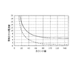
- FIG. 11 is a diagram showing the relationship between the normalized cell current value and the count value depending on whether or not the constant current source 140 is present.
- the horizontal axis represents the count value of the counter 134
- the vertical axis represents the normalized cell current value.
- the standardized cell current value is a standardized current assuming that there is no leakage current when a predetermined voltage is applied to the memory cell.
- the count value on the horizontal axis corresponds to the count value corresponding to the resistance value information of the memory cell. That is, the correlation between the count value of the resistance value information read by the read circuit 7b and the actual cell current amount is shown.
- a graph represented by a dotted line in FIG. 11 represents the count value of the memory cell and the normalized cell current value when SW4 is OFF.
- a graph represented by a solid line in FIG. 11 represents the count value of the memory cell and the normalized cell current value when SW4 is on.
- the count value in the region where the cell resistance value of the selected cell is low is larger when SW4 is turned on. That is, when the normalized cell current value is the same, the resolution of the resistance value information in the low resistance value region (the region where the cell current value is large) is improved.
- the method of increasing the count value with the constant current source 140 is effective when the resistance value of the memory cell is lowered by repeating the forming operation. This is because, when the resistance value of the memory cell is low, the discharge time is shortened and the count value is reduced, so that the measurement accuracy of the resistance value of the memory cell is lowered. That is, according to the resistance value of the memory cell, SW4 is turned ON / OFF, and the current amount of the constant current source is increased stepwise in N stages, thereby reducing the resistance measurement range from the high resistance side. Switching to the resistance side is made plural (correcting the count value). In FIG. 11, only two typical characteristics are illustrated.
- the method of improving the measured value of the memory cell is not limited to the method of adding the constant current source 140.
- the resolution of the resistance value information can be improved by increasing the clock frequency input to the counter 134. Further, the resolution of the resistance value information can be improved by lowering the reference voltage Vref2, and can be improved by increasing the capacitance of the capacitor CC2.
- the system controller 9 can freely set the resolution of the resistance value information by adjusting the predetermined current amount of the constant current source 140, the clock frequency, the voltage of the reference voltage Vref2, and the capacitance of the capacitor CC2. .
- the system controller 9 shifts the measurement range so that a high resistance value can be read by decreasing the current amount of the constant current source 140, increasing the reference voltage Vref2, and decreasing the capacitance of the capacitor CC2. be able to.
- the system controller 9 decreases the voltage level of Vref2, increases the current of the constant current source 140, and increases the capacitance of the capacitor CC2.
- the range can be shifted.
- the capacitance of the capacitor CC2 can be changed by switching the capacitor CC2 to a capacitor having a different capacitance value with a switch element or the like.
- the method of improving the measurement system by shifting the measurement range of the resistance value is very effective in a nonvolatile memory device using a resistance change element that requires a forming process.
- the amount of change in the resistance value of the memory cell due to the application of the forming voltage reaches 1 to 2 digits in the resistance value.
- the method of shifting the measurement range is very effective.
- the forming voltage applied to the memory cell in forming is larger than the voltage used for normal resistance change operation.
- a forming voltage is repeatedly applied to a resistance change element of a memory cell having an extremely high resistance value, which was initially in an insulated state, and a memory cell having a reduced resistance value due to application of the forming voltage, the memory cell
- the electrical stress applied to the voltage increases as the resistance value decreases.
- the system controller 9 reduces the forming voltage as the resistance value indicated by the resistance value information read by the readout circuit 7b decreases while the application of the forming voltage is repeated. You may control so that it may become low. Further, the system controller 9 may perform control so that the pulse width of the forming voltage becomes smaller as the resistance value represented by the resistance value information read out by the readout circuit 7b becomes lower while the application of the forming voltage is repeated.
- the correlation between the resistance value information is obtained before and after the measurement range shift, so that the forming threshold obtained from the initial resistance value information and the measured value after the shift of the measurement range are simplified. Can be compared.
- the leakage current in the cross-point type memory cell array slows down as the path is farther from the selected memory cell. This is due to the wiring resistance of the wirings constituting the memory cell array and the parasitic capacitance in each path path. Therefore, if the resistance value of the selected memory cell can be read faster and in a shorter time, the influence of the leakage current is alleviated.
- the readout circuit 7b since the readout circuit 7b reads out the resistance value according to the discharge time, the resistance value can be read out in a shorter time than the readout circuit 7a according to the first embodiment. Therefore, the read circuit 7b is also advantageous in that it is hardly affected by the leakage current.
- the resistance value immediately before forming is stored for each memory cell, and the resistance value obtained by multiplying the value by a predetermined ratio is stored.
- the threshold value automatically follows optimally, and appropriate forming can be performed.
- the measurement range of the resistance value can be easily changed, and high-precision forming is possible even when the resistance value is lowered during the forming process.
- the nonvolatile memory device As described above, the nonvolatile memory device according to one embodiment of the present invention has been described based on the embodiment.
- the cross-point type nonvolatile memory device in which the memory cell of the nonvolatile memory device includes the bidirectional current control element and the resistance change element has been described.
- a unidirectional current control element may be used instead of the bidirectional current control element.
- the non-volatile memory device may be other than the cross-point type non-volatile memory device.
- the non-volatile memory device is a one-transistor one-resistance (1T1R) type non-volatile memory device in which a memory cell includes a transistor and a resistance change element. May be.
- the initial resistance value does not fluctuate with an increase in leakage current, but the resistance value varies from lot to lot, or the resistance value varies depending on the cell position on the memory array. Can occur. Therefore, by applying a forming method similar to that described above, it is possible to perform forming following these deviations.
- the case where the electrical stress applied to the variable resistance element during the forming process varies according to the leakage current has been described.
- the forming method described in the above embodiment is used in other cases. Is also applicable.
- the forming method described in the above embodiment is also useful when the electrical stress applied to the resistance change element during the forming process varies depending on the structure variation of the memory cells.
- the reading circuit described in the above embodiment is an example, and the present invention is not limited to the structure described in the above embodiment.
- a capacitor is used as the storage unit.
- the storage unit may have any form as long as it can store resistance value information.
- the capacitor used as the storage unit may be a capacitive load, and the form is not limited.
- the capacitor used as the storage unit may be, for example, a diffusion capacitance of a transistor having a high affinity for a semiconductor process.
- the nonvolatile memory device includes a memory cell, a voltage application unit that applies a voltage to the memory cell, a read unit that reads resistance value information of the memory cell, and resistance value information read from the memory cell by the read unit.
- this invention is not limited to these embodiment or its modification. Unless it deviates from the gist of the present invention, various modifications conceived by those skilled in the art are applied to the present embodiment or the modification thereof, or a form constructed by combining different embodiments or components in the modification. Included within the scope of the present invention.
- the present invention is particularly useful as a nonvolatile memory device including a resistance change element that can stably change resistance by performing an appropriate forming process on the resistance change element among the nonvolatile memory devices. .
Landscapes
- Engineering & Computer Science (AREA)
- Chemical & Material Sciences (AREA)
- Materials Engineering (AREA)
- Computer Hardware Design (AREA)
- Semiconductor Memories (AREA)
Abstract
Priority Applications (2)
| Application Number | Priority Date | Filing Date | Title |
|---|---|---|---|
| US14/123,787 US9183925B2 (en) | 2012-04-09 | 2013-04-04 | Variable resistance nonvolatile memory device and method of performing the forming operation |
| JP2013553723A JP5479657B1 (ja) | 2012-04-09 | 2013-04-04 | 不揮発性記憶装置、およびそのフォーミング方法 |
Applications Claiming Priority (2)
| Application Number | Priority Date | Filing Date | Title |
|---|---|---|---|
| JP2012088629 | 2012-04-09 | ||
| JP2012-088629 | 2012-04-09 |
Publications (1)
| Publication Number | Publication Date |
|---|---|
| WO2013153786A1 true WO2013153786A1 (fr) | 2013-10-17 |
Family
ID=49327371
Family Applications (1)
| Application Number | Title | Priority Date | Filing Date |
|---|---|---|---|
| PCT/JP2013/002339 WO2013153786A1 (fr) | 2012-04-09 | 2013-04-04 | Dispositif de stockage non volatil et procédé pour sa formation |
Country Status (3)
| Country | Link |
|---|---|
| US (1) | US9183925B2 (fr) |
| JP (1) | JP5479657B1 (fr) |
| WO (1) | WO2013153786A1 (fr) |
Families Citing this family (12)
| Publication number | Priority date | Publication date | Assignee | Title |
|---|---|---|---|---|
| US9847125B2 (en) * | 2015-08-05 | 2017-12-19 | University Of Rochester | Resistive memory accelerator |
| US9576657B1 (en) * | 2015-09-29 | 2017-02-21 | Sandisk Technologies Llc | Memory cells including vertically oriented adjustable resistance structures |
| DE102017203455A1 (de) * | 2016-03-02 | 2017-09-07 | Infineon Technologies Ag | Übergangsüberwachung bei resistivem Speicher |
| US9837153B1 (en) * | 2017-03-24 | 2017-12-05 | Western Digital Technologies, Inc. | Selecting reversible resistance memory cells based on initial resistance switching |
| US12014770B2 (en) | 2017-10-17 | 2024-06-18 | R&D3 Llc | Memory device having variable impedance memory cells and time-to-transition sensing of data stored therein |
| US10269413B1 (en) | 2017-10-17 | 2019-04-23 | R&D 3 Llc | Memory device having variable impedance memory cells and time-to-transition sensing of data stored therein |
| US11501826B2 (en) | 2017-10-17 | 2022-11-15 | R&D3 Llc | Memory device having variable impedance memory cells and time-to-transition sensing of data stored therein |
| CN108230993A (zh) * | 2018-03-12 | 2018-06-29 | 厦门强力巨彩光电科技有限公司 | 一种带有存储单元的led显示模组及其控制方法 |
| TWI666647B (zh) * | 2018-09-03 | 2019-07-21 | 瑞昱半導體股份有限公司 | 記憶體裝置 |
| CN110635029A (zh) * | 2019-09-17 | 2019-12-31 | 天津理工大学 | 一种双波段光加密阻变存储器及其制备方法、写入方法和读取方法 |
| CN112735494B (zh) * | 2021-01-04 | 2022-09-30 | 中国人民解放军国防科技大学 | 忆阻器阻值调控方法、装置、计算机终端及存储介质 |
| US11915749B2 (en) | 2021-05-14 | 2024-02-27 | Ememory Technology Inc. | Resistive memory device and forming method thereof with improved forming time and improved forming uniformity |
Citations (3)
| Publication number | Priority date | Publication date | Assignee | Title |
|---|---|---|---|---|
| WO2011121971A1 (fr) * | 2010-03-30 | 2011-10-06 | パナソニック株式会社 | Dispositif de mémoire non volatile et procédé d'écriture dans un dispositif de mémoire non volatile |
| JP2011204289A (ja) * | 2010-03-24 | 2011-10-13 | Toshiba Corp | 不揮発性半導体記憶装置 |
| JP2012038398A (ja) * | 2010-08-11 | 2012-02-23 | Toshiba Corp | 半導体記憶装置 |
Family Cites Families (17)
| Publication number | Priority date | Publication date | Assignee | Title |
|---|---|---|---|---|
| JP3800925B2 (ja) * | 2000-05-15 | 2006-07-26 | 日本電気株式会社 | 磁気ランダムアクセスメモリ回路 |
| US6791859B2 (en) * | 2001-11-20 | 2004-09-14 | Micron Technology, Inc. | Complementary bit PCRAM sense amplifier and method of operation |
| JP2005032401A (ja) | 2003-06-17 | 2005-02-03 | Sharp Corp | 不揮発性半導体記憶装置及びその書き込み方法と消去方法 |
| US6970387B2 (en) | 2003-09-15 | 2005-11-29 | Hewlett-Packard Development Company, L.P. | System and method for determining the value of a memory element |
| JP4153901B2 (ja) | 2004-06-15 | 2008-09-24 | シャープ株式会社 | 半導体記憶装置 |
| US7869253B2 (en) | 2006-08-21 | 2011-01-11 | Qimonda Ag | Method of determining a memory state of a resistive memory cell and device measuring the memory state of a resistive memory cell |
| JP4774109B2 (ja) | 2009-03-13 | 2011-09-14 | シャープ株式会社 | 不揮発性可変抵抗素子のフォーミング処理の制御回路、並びにフォーミング処理の制御方法 |
| JP5197448B2 (ja) * | 2009-03-13 | 2013-05-15 | 株式会社東芝 | 抵抗変化メモリ装置 |
| CN102099863B (zh) * | 2009-06-08 | 2014-04-02 | 松下电器产业株式会社 | 电阻变化型非易失性存储元件的写入方法及电阻变化型非易失性存储装置 |
| US7965565B2 (en) | 2009-07-13 | 2011-06-21 | Seagate Technology Llc | Current cancellation for non-volatile memory |
| JP4940287B2 (ja) | 2009-08-06 | 2012-05-30 | 株式会社東芝 | 不揮発性半導体記憶装置 |
| JP2011066363A (ja) | 2009-09-18 | 2011-03-31 | Toshiba Corp | 半導体装置及びその製造方法 |
| JP5121864B2 (ja) | 2010-03-02 | 2013-01-16 | 株式会社東芝 | 不揮発性半導体記憶装置 |
| US8498141B2 (en) | 2010-03-24 | 2013-07-30 | Kabushiki Kaisha Toshiba | Non-volatile semiconductor memory device |
| JP2011198445A (ja) | 2010-03-24 | 2011-10-06 | Toshiba Corp | 半導体記憶装置 |
| WO2011121970A1 (fr) | 2010-03-30 | 2011-10-06 | パナソニック株式会社 | Procédé de formation d'un élément de mémoire non volatile à résistance variable et dispositif de mémoire non volatile à résistance variable |
| JP5390732B1 (ja) * | 2011-12-07 | 2014-01-15 | パナソニック株式会社 | クロスポイント型不揮発性記憶装置とそのフォーミング方法 |
-
2013
- 2013-04-04 WO PCT/JP2013/002339 patent/WO2013153786A1/fr active Application Filing
- 2013-04-04 US US14/123,787 patent/US9183925B2/en active Active
- 2013-04-04 JP JP2013553723A patent/JP5479657B1/ja active Active
Patent Citations (3)
| Publication number | Priority date | Publication date | Assignee | Title |
|---|---|---|---|---|
| JP2011204289A (ja) * | 2010-03-24 | 2011-10-13 | Toshiba Corp | 不揮発性半導体記憶装置 |
| WO2011121971A1 (fr) * | 2010-03-30 | 2011-10-06 | パナソニック株式会社 | Dispositif de mémoire non volatile et procédé d'écriture dans un dispositif de mémoire non volatile |
| JP2012038398A (ja) * | 2010-08-11 | 2012-02-23 | Toshiba Corp | 半導体記憶装置 |
Also Published As
| Publication number | Publication date |
|---|---|
| JP5479657B1 (ja) | 2014-04-23 |
| JPWO2013153786A1 (ja) | 2015-12-17 |
| US9183925B2 (en) | 2015-11-10 |
| US20140104931A1 (en) | 2014-04-17 |
Similar Documents
| Publication | Publication Date | Title |
|---|---|---|
| JP5479657B1 (ja) | 不揮発性記憶装置、およびそのフォーミング方法 | |
| JP4722230B2 (ja) | 不揮発性記憶装置及び不揮発性記憶装置へのデータ書込み方法 | |
| CN110036444B (zh) | 自适应存储器单元写入条件 | |
| JP4940287B2 (ja) | 不揮発性半導体記憶装置 | |
| CN103339682B (zh) | 交叉点型非易失性存储装置及其成形方法 | |
| JP5655173B2 (ja) | クロスポイント型不揮発性記憶装置とその駆動方法 | |
| CN103052990B (zh) | 电阻变化型非易失性存储装置及其驱动方法 | |
| JP4383523B2 (ja) | 不揮発性記憶素子及び不揮発性半導体記憶装置、並びにそれらの読み出し方法及び書き込み方法 | |
| WO2013080499A1 (fr) | Procédé d'écriture d'élément de stockage non volatil de type à changement de résistance, et dispositif de stockage non volatil de type à changement de résistance | |
| JP5548319B2 (ja) | 不揮発性記憶素子の駆動方法 | |
| WO2011045886A1 (fr) | Dispositif de mémoire non volatile du type à changement de résistance | |
| JP5069339B2 (ja) | 不揮発性可変抵抗素子の抵抗制御方法 | |
| CN102612716B (zh) | 非易失性存储装置 | |
| JP2006202411A (ja) | 不揮発性半導体記憶装置及びその制御方法 | |
| JP2014238897A (ja) | 抵抗変化型不揮発性記憶装置およびその制御方法 | |
| US7855910B2 (en) | Electric element, memory device, and semiconductor integrated circuit | |
| US10490276B2 (en) | Non-volatile storage device and driving method | |
| US9142292B2 (en) | Method for reading data from nonvolatile storage element, and nonvolatile storage device | |
| CN111667864B (zh) | 半导体存储装置以及方法 | |
| US20230081445A1 (en) | Variable resistance nonvolatile storage device and write method therefor |
Legal Events
| Date | Code | Title | Description |
|---|---|---|---|
| ENP | Entry into the national phase |
Ref document number: 2013553723 Country of ref document: JP Kind code of ref document: A |
|
| 121 | Ep: the epo has been informed by wipo that ep was designated in this application |
Ref document number: 13775509 Country of ref document: EP Kind code of ref document: A1 |
|
| WWE | Wipo information: entry into national phase |
Ref document number: 14123787 Country of ref document: US |
|
| NENP | Non-entry into the national phase |
Ref country code: DE |
|
| 122 | Ep: pct application non-entry in european phase |
Ref document number: 13775509 Country of ref document: EP Kind code of ref document: A1 |