WO2013146446A1 - 炭化珪素半導体素子及びその製造方法 - Google Patents
炭化珪素半導体素子及びその製造方法 Download PDFInfo
- Publication number
- WO2013146446A1 WO2013146446A1 PCT/JP2013/057740 JP2013057740W WO2013146446A1 WO 2013146446 A1 WO2013146446 A1 WO 2013146446A1 JP 2013057740 W JP2013057740 W JP 2013057740W WO 2013146446 A1 WO2013146446 A1 WO 2013146446A1
- Authority
- WO
- WIPO (PCT)
- Prior art keywords
- layer
- tic
- thin film
- silicon carbide
- thin
- Prior art date
- Legal status (The legal status is an assumption and is not a legal conclusion. Google has not performed a legal analysis and makes no representation as to the accuracy of the status listed.)
- Ceased
Links
Images





Classifications
-
- H—ELECTRICITY
- H10—SEMICONDUCTOR DEVICES; ELECTRIC SOLID-STATE DEVICES NOT OTHERWISE PROVIDED FOR
- H10D—INORGANIC ELECTRIC SEMICONDUCTOR DEVICES
- H10D62/00—Semiconductor bodies, or regions thereof, of devices having potential barriers
- H10D62/80—Semiconductor bodies, or regions thereof, of devices having potential barriers characterised by the materials
- H10D62/83—Semiconductor bodies, or regions thereof, of devices having potential barriers characterised by the materials being Group IV materials, e.g. B-doped Si or undoped Ge
- H10D62/832—Semiconductor bodies, or regions thereof, of devices having potential barriers characterised by the materials being Group IV materials, e.g. B-doped Si or undoped Ge being Group IV materials comprising two or more elements, e.g. SiGe
- H10D62/8325—Silicon carbide
-
- H—ELECTRICITY
- H10—SEMICONDUCTOR DEVICES; ELECTRIC SOLID-STATE DEVICES NOT OTHERWISE PROVIDED FOR
- H10D—INORGANIC ELECTRIC SEMICONDUCTOR DEVICES
- H10D64/00—Electrodes of devices having potential barriers
-
- H—ELECTRICITY
- H10—SEMICONDUCTOR DEVICES; ELECTRIC SOLID-STATE DEVICES NOT OTHERWISE PROVIDED FOR
- H10D—INORGANIC ELECTRIC SEMICONDUCTOR DEVICES
- H10D64/00—Electrodes of devices having potential barriers
- H10D64/01—Manufacture or treatment
- H10D64/011—Manufacture or treatment of electrodes ohmically coupled to a semiconductor
- H10D64/0111—Manufacture or treatment of electrodes ohmically coupled to a semiconductor to Group IV semiconductors
- H10D64/0115—Manufacture or treatment of electrodes ohmically coupled to a semiconductor to Group IV semiconductors to silicon carbide
-
- H—ELECTRICITY
- H10—SEMICONDUCTOR DEVICES; ELECTRIC SOLID-STATE DEVICES NOT OTHERWISE PROVIDED FOR
- H10D—INORGANIC ELECTRIC SEMICONDUCTOR DEVICES
- H10D64/00—Electrodes of devices having potential barriers
- H10D64/60—Electrodes characterised by their materials
-
- H—ELECTRICITY
- H10—SEMICONDUCTOR DEVICES; ELECTRIC SOLID-STATE DEVICES NOT OTHERWISE PROVIDED FOR
- H10D—INORGANIC ELECTRIC SEMICONDUCTOR DEVICES
- H10D64/00—Electrodes of devices having potential barriers
- H10D64/60—Electrodes characterised by their materials
- H10D64/62—Electrodes ohmically coupled to a semiconductor
-
- H—ELECTRICITY
- H10—SEMICONDUCTOR DEVICES; ELECTRIC SOLID-STATE DEVICES NOT OTHERWISE PROVIDED FOR
- H10D—INORGANIC ELECTRIC SEMICONDUCTOR DEVICES
- H10D64/00—Electrodes of devices having potential barriers
- H10D64/60—Electrodes characterised by their materials
- H10D64/64—Electrodes comprising a Schottky barrier to a semiconductor
-
- H—ELECTRICITY
- H10—SEMICONDUCTOR DEVICES; ELECTRIC SOLID-STATE DEVICES NOT OTHERWISE PROVIDED FOR
- H10P—GENERIC PROCESSES OR APPARATUS FOR THE MANUFACTURE OR TREATMENT OF DEVICES COVERED BY CLASS H10
- H10P14/00—Formation of materials, e.g. in the shape of layers or pillars
- H10P14/40—Formation of materials, e.g. in the shape of layers or pillars of conductive or resistive materials
-
- H—ELECTRICITY
- H10—SEMICONDUCTOR DEVICES; ELECTRIC SOLID-STATE DEVICES NOT OTHERWISE PROVIDED FOR
- H10D—INORGANIC ELECTRIC SEMICONDUCTOR DEVICES
- H10D30/00—Field-effect transistors [FET]
- H10D30/60—Insulated-gate field-effect transistors [IGFET]
-
- H—ELECTRICITY
- H10—SEMICONDUCTOR DEVICES; ELECTRIC SOLID-STATE DEVICES NOT OTHERWISE PROVIDED FOR
- H10D—INORGANIC ELECTRIC SEMICONDUCTOR DEVICES
- H10D8/00—Diodes
- H10D8/60—Schottky-barrier diodes
-
- H—ELECTRICITY
- H10—SEMICONDUCTOR DEVICES; ELECTRIC SOLID-STATE DEVICES NOT OTHERWISE PROVIDED FOR
- H10W—GENERIC PACKAGES, INTERCONNECTIONS, CONNECTORS OR OTHER CONSTRUCTIONAL DETAILS OF DEVICES COVERED BY CLASS H10
- H10W72/00—Interconnections or connectors in packages
- H10W72/071—Connecting or disconnecting
- H10W72/073—Connecting or disconnecting of die-attach connectors
-
- H—ELECTRICITY
- H10—SEMICONDUCTOR DEVICES; ELECTRIC SOLID-STATE DEVICES NOT OTHERWISE PROVIDED FOR
- H10W—GENERIC PACKAGES, INTERCONNECTIONS, CONNECTORS OR OTHER CONSTRUCTIONAL DETAILS OF DEVICES COVERED BY CLASS H10
- H10W72/00—Interconnections or connectors in packages
- H10W72/071—Connecting or disconnecting
- H10W72/073—Connecting or disconnecting of die-attach connectors
- H10W72/07331—Connecting techniques
- H10W72/07336—Soldering or alloying
-
- H—ELECTRICITY
- H10—SEMICONDUCTOR DEVICES; ELECTRIC SOLID-STATE DEVICES NOT OTHERWISE PROVIDED FOR
- H10W—GENERIC PACKAGES, INTERCONNECTIONS, CONNECTORS OR OTHER CONSTRUCTIONAL DETAILS OF DEVICES COVERED BY CLASS H10
- H10W72/00—Interconnections or connectors in packages
- H10W72/071—Connecting or disconnecting
- H10W72/075—Connecting or disconnecting of bond wires
-
- H—ELECTRICITY
- H10—SEMICONDUCTOR DEVICES; ELECTRIC SOLID-STATE DEVICES NOT OTHERWISE PROVIDED FOR
- H10W—GENERIC PACKAGES, INTERCONNECTIONS, CONNECTORS OR OTHER CONSTRUCTIONAL DETAILS OF DEVICES COVERED BY CLASS H10
- H10W72/00—Interconnections or connectors in packages
- H10W72/071—Connecting or disconnecting
- H10W72/075—Connecting or disconnecting of bond wires
- H10W72/07531—Techniques
- H10W72/07532—Compression bonding, e.g. thermocompression bonding
- H10W72/07533—Ultrasonic bonding, e.g. thermosonic bonding
-
- H—ELECTRICITY
- H10—SEMICONDUCTOR DEVICES; ELECTRIC SOLID-STATE DEVICES NOT OTHERWISE PROVIDED FOR
- H10W—GENERIC PACKAGES, INTERCONNECTIONS, CONNECTORS OR OTHER CONSTRUCTIONAL DETAILS OF DEVICES COVERED BY CLASS H10
- H10W72/00—Interconnections or connectors in packages
- H10W72/50—Bond wires
- H10W72/551—Materials of bond wires
- H10W72/552—Materials of bond wires comprising metals or metalloids, e.g. silver
- H10W72/5524—Materials of bond wires comprising metals or metalloids, e.g. silver comprising aluminium [Al]
-
- H—ELECTRICITY
- H10—SEMICONDUCTOR DEVICES; ELECTRIC SOLID-STATE DEVICES NOT OTHERWISE PROVIDED FOR
- H10W—GENERIC PACKAGES, INTERCONNECTIONS, CONNECTORS OR OTHER CONSTRUCTIONAL DETAILS OF DEVICES COVERED BY CLASS H10
- H10W72/00—Interconnections or connectors in packages
- H10W72/851—Dispositions of multiple connectors or interconnections
- H10W72/874—On different surfaces
- H10W72/884—Die-attach connectors and bond wires
-
- H—ELECTRICITY
- H10—SEMICONDUCTOR DEVICES; ELECTRIC SOLID-STATE DEVICES NOT OTHERWISE PROVIDED FOR
- H10W—GENERIC PACKAGES, INTERCONNECTIONS, CONNECTORS OR OTHER CONSTRUCTIONAL DETAILS OF DEVICES COVERED BY CLASS H10
- H10W72/00—Interconnections or connectors in packages
- H10W72/90—Bond pads, in general
- H10W72/921—Structures or relative sizes of bond pads
- H10W72/923—Bond pads having multiple stacked layers
-
- H—ELECTRICITY
- H10—SEMICONDUCTOR DEVICES; ELECTRIC SOLID-STATE DEVICES NOT OTHERWISE PROVIDED FOR
- H10W—GENERIC PACKAGES, INTERCONNECTIONS, CONNECTORS OR OTHER CONSTRUCTIONAL DETAILS OF DEVICES COVERED BY CLASS H10
- H10W72/00—Interconnections or connectors in packages
- H10W72/90—Bond pads, in general
- H10W72/951—Materials of bond pads
- H10W72/952—Materials of bond pads comprising metals or metalloids, e.g. PbSn, Ag or Cu
-
- H—ELECTRICITY
- H10—SEMICONDUCTOR DEVICES; ELECTRIC SOLID-STATE DEVICES NOT OTHERWISE PROVIDED FOR
- H10W—GENERIC PACKAGES, INTERCONNECTIONS, CONNECTORS OR OTHER CONSTRUCTIONAL DETAILS OF DEVICES COVERED BY CLASS H10
- H10W90/00—Package configurations
- H10W90/701—Package configurations characterised by the relative positions of pads or connectors relative to package parts
- H10W90/751—Package configurations characterised by the relative positions of pads or connectors relative to package parts of bond wires
- H10W90/754—Package configurations characterised by the relative positions of pads or connectors relative to package parts of bond wires between a chip and a stacked insulating package substrate, interposer or RDL
Definitions
- the present invention relates to a semiconductor element using silicon carbide (hereinafter also referred to as “SiC”) as a semiconductor material, and more particularly to a vertical power device semiconductor element in which current flows from the front side to the back side and a method for manufacturing the same.
- SiC silicon carbide
- silicon carbide semiconductor Since silicon carbide semiconductor has a larger band gap than silicon semiconductor, it has a high dielectric breakdown electric field strength.
- the on-resistance which is a resistance in a conductive state, is inversely proportional to the cube of the dielectric breakdown electric field strength. For this reason, for example, in a widely used silicon carbide semiconductor called 4H type, the on-resistance can be suppressed to several hundredths of that of a silicon semiconductor. Accordingly, a semiconductor element using a silicon carbide semiconductor is expected as a next-generation low-loss power semiconductor element in combination with a large thermal conductivity characteristic that facilitates heat dissipation.
- a power semiconductor element has a vertical structure in which a current flows from the front side to the back side of a wafer. Since the ratio of the electrode pad to the total area of the elements cannot be ignored, the main reason is that the same current can be realized in a smaller area by forming one electrode on the back surface of the wafer.
- the back electrode is bonded to a copper (Cu) plate called DBC (Direct Bonded Copper) via a solder layer.
- DBC Direct Bonded Copper
- the front surface electrode is bonded to one end of an aluminum (Al) wire by ultrasonic waves, and the other end of the Al wire is bonded to DBC.
- Ni 2 Si nickel silicide
- a good value of a contact resistance of 10 ⁇ 7 ⁇ cm 2 is obtained with respect to a substrate (wafer) concentration of 10 19 cm ⁇ 3 (see, for example, Non-Patent Document 1 below) ).
- carbon having a graphite structure is formed on the outermost surface as can be seen from the reaction formula of the following formula (1).
- a part of this graphite is deposited on the surface of the Ni 2 Si layer which is stable in terms of energy.
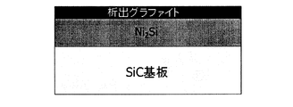
- FIG. 2 is a diagram schematically showing a layer structure at a stage where an ohmic layer is formed by sintering after depositing Ni on a SiC substrate.
- a structure of graphite layer / Ni 2 Si layer / SiC substrate is formed from the surface side (exposed surface side) of the ohmic layer.
- a multilayer film in which, for example, titanium (Ti), Ni, and gold (Au) are sequentially deposited is formed on the ohmic layer, but the multilayer is formed by the graphite layer deposited on the outermost surface of the ohmic layer. It is known that film peeling occurs (for example, see Non-Patent Document 2 below).
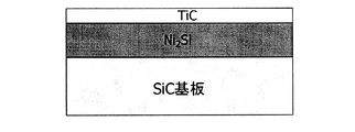
- FIG. 3 is a diagram schematically showing a layer configuration at a stage where an ohmic layer is formed by sintering after depositing Ni and Ti on a SiC substrate.
- the layer structure from the surface side of the ohmic layer at the stage of forming the ohmic layer is a TiC layer / Ni 2 Si layer / SiC substrate as shown in FIG. 3 (for example, the following non-patent document) 3).
- a three-layer film composed of Ti, Ni, and Au is not formed immediately after the ohmic layer is formed, and there are various processes depending on the type of device.
- the steps after the formation of the ohmic layer are performed on the wafer front surface side, such as Schottky contact hole formation, Schottky metal formation, Al—Si metal. Formation, polyimide layer formation.
- the ohmic layer forming step is performed before these steps is that the sintering temperature of the ohmic layer is as high as 900 ° C. or higher.
- the three-layer film made of Ti, Ni, and Au is implemented at the end of the preceding process (the ohmic layer forming process, the above-described processes performed on the wafer front side and the three-layer film forming process) This is to prevent cross-contamination into the Au production line.
- the three-layer film made of Ti, Ni, and Au deposited at the end of the previous process is referred to as “back-surface three-layer metal”.
- the present invention has been made in view of these problems, and provides a silicon carbide semiconductor element that does not cause peeling of a back electrode even after wafer dicing and subsequent pickup from a dicing tape, and a method for manufacturing the same. It is the purpose.
- a Ni 2 Si layer formed by sintering after depositing a thin layer made of Ni and a thin layer containing Ti on a silicon carbide substrate and A thin film (ohmic layer) composed of a TiC layer has a structure in which a TiC layer is deposited on the surface, and a multilayer thin film including a Ti layer as a first thin film and a Ni layer as a second thin film on the surface of the TiC layer. It has been found that in a sequentially deposited back electrode structure, the C composition ratio derived from TiC at the interface between the TiC layer and the Ti layer of the multilayer thin film should be 15% or more.
- a step of forming a thin film (ohmic layer) composed of a Ni 2 Si layer and a TiC layer with the TiC layer as the front side, a Ti layer as a first thin film on the ohmic layer It has also been found that a step of depositing a Ti thin film on the TiC layer may be inserted between the step of sequentially depositing a multilayer thin film including a Ni layer as the second thin film.
- a silicon carbide semiconductor device has the following characteristics.
- a thin film made of Ni 2 Si and TiC formed by depositing a thin layer made of Ni and a thin layer made of Ti provided on a silicon carbide substrate is formed by depositing the TiC on the surface.
- the structure has a layer made of TiC.
- a multilayer thin film including a Ti layer as a first thin film and a Ni layer as a second thin film is formed on the surface of the layer made of TiC.
- the C composition ratio derived from the TiC layer is 15% or more at the interface between the TiC layer and the Ti layer of the multilayer thin film.
- a method for manufacturing a silicon carbide semiconductor device is the above-described method for manufacturing a silicon carbide semiconductor device, and has the following characteristics.
- step (A) of depositing a thin layer made of Ni and a thin layer made of Ti on a silicon carbide substrate is performed.
- step (B) of forming is performed.
- a step (C) of forming a multilayer thin film including a Ti layer as the first thin film and a Ni layer as the second thin film on the surface of the layer made of TiC is performed. Then, in the step (A) for depositing the thin layer, the film thickness ratio (Ti / Ni) of the thin layer composed of Ti and the thin layer composed of Ni is set to 0.25 to 0.67.
- the method for manufacturing a silicon carbide semiconductor device according to the present invention is the method described above, wherein the Ti thin film is deposited between the sintering step (B) and the multilayer thin film forming step (C). It has the process (D) to perform, It is characterized by the above-mentioned.
- the silicon carbide semiconductor device and the method for manufacturing the same according to the present invention it is possible to obtain a silicon carbide semiconductor device in which the back electrode is not peeled even after wafer dicing and subsequent pickup from the dicing tape. .
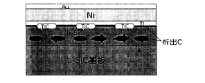
- FIG. 1 is a diagram schematically showing a layer configuration of an embodiment of the silicon carbide semiconductor device of the present invention.
- FIG. 2 is a diagram schematically showing a layer structure at a stage where an ohmic layer is formed by sintering after depositing Ni on a SiC substrate.
- FIG. 3 is a diagram schematically showing a layer configuration at a stage where an ohmic layer is formed by sintering after depositing Ni and Ti on a SiC substrate.
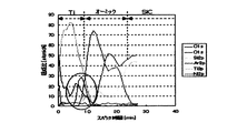
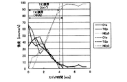
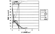
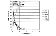
- FIG. 4A is a diagram in which the profile in the depth direction of each element in the vicinity of the peeling interface of the wafer is measured by X-ray photoelectron spectroscopy (XPS).
- XPS X-ray photoelectron spectroscopy
- FIG. 4B is a diagram in which the profile in the depth direction of each element in the closely contacted portion of the wafer is measured by X-ray photoelectron spectroscopy (XPS).
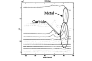
- FIG. 5A is a diagram illustrating a C1s spectrum by XPS.
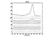
- FIG. 5-2 is a diagram showing a Ti2p spectrum by XPS.
- FIG. 5-3 is a diagram showing an O1s spectrum by XPS.
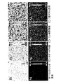
- FIG. 6 is a diagram showing a transition of AES mapping (10 ⁇ m) of Ti (upper stage) and Ni (lower stage).
- FIG. 7-1 is a diagram illustrating a result of measuring a depth profile of Ti and C by XPS immediately after sintering for obtaining ohmic contact with a silicon carbide semiconductor.
- FIG. 7-2 is a diagram showing the results of measuring the profile in the depth direction of Ti and C by XPS after the ammonia overwater treatment.
- FIG. 7-3 is a diagram showing a result of measuring a depth profile of Ti and C by XPS after phosphoric acid acetic acid etching.
- FIG. 7-4 is a diagram showing a result of measuring a depth profile of Ti and C by XPS after BHF etching.
- FIG. 8 is a diagram showing a correlation between the carbon composition derived from TiC at the interface between the ohmic layer and the Ti layer of the back surface three-layer metal and the presence or absence of peeling of the back surface three-layer metal.
- FIG. 9 is a diagram showing the correlation between the thickness of the Ti protective thin film and the yield (ratio of elements in which peeling did not occur) in Example 2.
- FIG. 10 is a diagram showing the results of the power cycle test.
- FIG. 1 is a diagram schematically showing a layer configuration of an embodiment of the silicon carbide semiconductor device of the present invention.
- the silicon carbide semiconductor element of the present invention is formed of Ni 2 Si formed by sintering after depositing a thin layer made of Ni and a thin layer made of Ti on a silicon carbide (SiC) substrate.
- a thin film (ohmic layer) comprising a layer and a TiC layer is provided, and a TiC layer is deposited on the surface of the ohmic layer.
- a multilayer thin film (back surface three-layer metal) including a Ti layer as a first thin film and a Ni layer as a second thin film is sequentially deposited on the surface of the TiC layer. Then, the separation of the back surface three-layer metal (Ti / Ni / Au) is prevented by increasing the C composition ratio derived from the TiC layer to 15% or more at the interface between the TiC layer and the Ti layer of the first thin film. Is.
- the delamination location in the depth direction was investigated, and it was found that the delamination surface was the interface between the ohmic layer and the Ti layer of the backside three-layer metal in any wafer.
- the profile in the depth direction of each element in the vicinity of the peeling interface was measured by X-ray photoelectron spectroscopy (XPS).
- XPS X-ray photoelectron spectroscopy
- FIG. 4A is a diagram in which the profile in the depth direction of each element in the vicinity of the peeling interface of the wafer is measured by X-ray photoelectron spectroscopy (XPS).
- FIG. 4B is a diagram in which the profile in the depth direction of each element in the closely contacted portion of the wafer is measured by X-ray photoelectron spectroscopy (XPS).
- FIGS. 5-1 to 5-3 The C1s spectrum, Ti2p spectrum, and O1s spectrum are shown in FIGS. 5-1 to 5-3, respectively.
- FIG. 5A is a diagram illustrating a C1s spectrum by XPS.
- FIG. 5-2 is a diagram showing a Ti2p spectrum by XPS.
- FIG. 5-3 is a diagram showing an O1s spectrum by XPS.
- the TiC layer is etched by ammonia perwater and phosphorous nitric acid used in the manufacturing process, and not etched by BHF (buffered hydrofluoric acid) (reference: M. Eizenberg and S. P. Mararka, J. Appl. Phys., Vol.54, No. 6 (1983) pp. 3190-3194). For this reason, it was also expected that the TiC layer would have a mosaic shape due to etching with a chemical solution.
- the investigated wafers are (a) those subjected only to the ohmic layer forming step (that is, those immediately after sintering for obtaining ohmic contact with the silicon carbide semiconductor), (b) forming the Schottky metal from the ohmic layer forming step.
- FIG. 6 is a diagram showing a transition of AES mapping (10 ⁇ m) of Ti (upper stage) and Ni (lower stage).
- Ti is uniformly formed and Ni is hardly detected, so it is assumed that the TiC layer is uniformly deposited in the plane. Is done.
- the in-plane distribution of Ti became sparse, and the Ni peak increased in the region where the Ti peak decreased. From this, it was speculated that as the process proceeded, the TiC layer was partially etched, and the underlying Ni 2 Si layer was exposed, and the above assumed mechanism was verified.
- FIG. 7-1 to 7-4 show the measurement results of the depth profiles of Ti and C by XPS.
- FIG. 7-1 is a diagram illustrating a result of measuring a depth profile of Ti and C by XPS immediately after sintering for obtaining ohmic contact with a silicon carbide semiconductor.
- FIG. 7-2 is a diagram showing the results of measuring the profile in the depth direction of Ti and C by XPS after the ammonia overwater treatment.
- FIG. 7-3 is a diagram showing a result of measuring a depth profile of Ti and C by XPS after phosphoric acid acetic acid etching.
- FIG. 7-4 is a diagram showing a result of measuring a depth profile of Ti and C by XPS after BHF etching.
- 7A shows the wafer (a)
- FIG. 7-2 shows the wafer (b)
- FIG. 7-3 shows the wafer (c)
- FIG. 7-4 shows the wafer (d). Show.
- the first thing that can be understood is that as the process proceeds, the film thickness at which Ti and C are detected, that is, the film thickness of the TiC layer decreases. Further, it can be seen that the decrease in the thickness of the TiC layer in FIGS. 7-1 and 7-3 is large.
- the TiC layer is etched by passing through the process of ammonia perhydration, in FIG. 7-3 by passing through the process of phosphonitrate, and in FIG. 7-4, the process of buffered hydrofluoric acid is passed through. However, the TiC layer is hardly etched. From these results, it is considered that the cause of the etching of the TiC layer is due to the wet etching liquid used in each step, in particular, ammonia overwater and phosphorous nitric acid.
- annealing is performed at a temperature of 500 ° C. after the ammonia overwater treatment. Further, in the polyimide forming step after the formation of the Al—Si metal, annealing is performed at a temperature of 350 ° C. to cure the polyimide. According to a report by Tanimoto et al., Carbon that had been partially dispersed in the Ni 2 Si layer was re-diffused by annealing at 100 ° C. to 600 ° C., and deposited as graphite on the surface of the energy stable Ni 2 Si layer. (For example, refer to JP 2007-184571 A).
- the TiC layer of the ohmic layer in this step covers the surface of the Ni 2 Si layer
- carbon dispersed in Ni 2 Si layer is absorbed by the TiC layer.
- the dispersed carbon is deposited as graphite on the surface of the Ni 2 Si layer as it is.
- the surface of the ohmic layer is in a state where the TiC layer and graphite are mixed, and as the area of the graphite increases, the adhesion strength with the Ti layer of the backside three-layer metal decreases, finally Is considered to lead to peeling of the backside three-layer metal.
- the peeling state of the back surface three-layer metal was compared between the case where the annealing after the formation of the Schottky metal and the annealing when the polyimide was cured, and the case where the annealing was not performed.
- the evaluation method is the same as the above method. As a result, peeling of the backside three-layer metal was observed only when annealing was performed, and the validity of the above mechanism was proved.
- a 4H—SiC wafer was used as a wafer to be a substrate, and an n-type epitaxial layer having an impurity concentration of 1 ⁇ 10 16 cm ⁇ 3 and a film thickness of 10 ⁇ m, for example, was grown on the (0001) Si surface of the wafer. Then, an element was fabricated on this epitaxial layer by a general method. Subsequent front surface electrode and back electrode forming steps will be described below as examples. Hereinafter, a Schottky barrier diode will be described as an example. For a vertical element, for a pin (p-intrinsic-n) diode, an insulated gate field effect transistor (MOSFET), an insulated gate bipolar transistor (IGBT), etc. Is also applicable.
- MOSFET insulated gate field effect transistor
- IGBT insulated gate bipolar transistor
- Example 1 After immersing the wafer in a buffered hydrofluoric acid solution to remove the oxide film covering the back surface of the wafer, a thin layer made of Ni and a thin layer made of Ti are sequentially deposited on the back surface of the wafer.
- a deposition method at this time any method such as a sputtering method, an electron beam evaporation method, a resistance heating evaporation method, or the like may be used.
- a thin layer made of Ni and a thin layer made of Ti may be sequentially stacked.
- Ni and Ti alloy targets may be deposited simultaneously by sputtering or multi-source deposition to form Ni and Ti. You may form the thin layer which consists of an alloy containing.
- the thickness of the Ni layer needs to be within an appropriate range.
- the thickness of the thin layer made of Ni is too thin, the reaction between SiC in the wafer and Ni in the thin layer made of Ni is not sufficient in subsequent sintering to obtain ohmic contact with the silicon carbide semiconductor. Without increasing ohmic contact resistance.
- the film thickness of the thin layer made of Ni is too thick, the resistance component of the Ni 2 Si layer formed by the sintering for obtaining ohmic contact with the silicon carbide semiconductor thereafter cannot be ignored.
- the appropriate range of the thickness of the thin layer made of Ni is desirably 20 to 200 nm.
- the thickness of the thin layer made of Ti is set to an appropriate range.
- the film thickness of the thin layer made of Ti is too thin, the amount of TiC formed on the surface of the ohmic layer is reduced by the subsequent sintering for obtaining ohmic contact with the silicon carbide semiconductor.
- the thickness of the thin layer made of Ti is too thick, the resistance component of the TiC layer cannot be ignored. From such a viewpoint, it is desirable that the appropriate range of the thickness of the thin layer made of Ti is 5 to 100 nm.
- Example 1 the thickness of the thin layer made of Ni is changed to 10 nm, 20 nm, 30 nm, and 40 nm with respect to the thickness of 60 nm of the thin layer made of Ni, and the thin layer made of Ni and Ti are made.
- the correlation between the thickness of the thin layer and the peeling of the backside three-layer metal was investigated.
- the thin layer made of Ni and the thin layer made of Ti deposited in this way are sintered to obtain ohmic contact with the 4H—SiC substrate.
- the holding temperature of sintering for obtaining ohmic contact with the silicon carbide semiconductor is 900 ° C. or more and the holding time is 1 minute or more, and the ohmic contact resistance is reduced by increasing the holding temperature and holding time. Can do.
- the sintering holding temperature is set to a temperature lower than about 1200 ° C. which is the melting point of the oxide film.
- the gas atmosphere during sintering for obtaining ohmic contact with the silicon carbide semiconductor is vacuum, Ar, He. , H 2 and a mixed gas thereof.
- Example 1 as sintering conditions for obtaining ohmic contact with the silicon carbide semiconductor, the holding temperature during sintering was 1050 ° C., the holding time was 2 minutes, and the sintering atmosphere was normal pressure Ar.
- the Schottky contact hole forming step, the Schottky metal forming step, the Al—Si metal forming step, the polyimide forming step, and the back surface three-layer metal forming are performed as described above. It carries out in order of a process.
- the processes affecting the ohmic layer constituting the back electrode are: buffered hydrofluoric acid treatment at the time of forming the Schottky contact hole, Amminia overwater treatment at the time of Schottky metal patterning at the time of Schottky metal formation, and shot with the silicon carbide semiconductor. Sintering to obtain key contact, phosphorous acetic acid treatment at the time of forming Al—Si metal, annealing at the time of polyimide curing, and buffered hydrofluoric acid treatment just before the formation of the backside three-layer metal.
- the chemical treatment conditions are uniquely determined so that the oxide film, Schottky metal, and Al—Si metal formed on the front side of the wafer are completely patterned by each chemical.
- the temperature, time, and atmosphere are uniquely determined by the required Schottky interface characteristics.
- the sintering conditions are uniquely determined depending on the material and film thickness in order to obtain Schottky contact with the silicon carbide semiconductor. Therefore, the details of these conditions are omitted.
- FIG. 8 is a diagram showing a correlation between the carbon composition derived from TiC at the interface between the ohmic layer and the Ti layer of the back surface three-layer metal and the presence or absence of peeling of the back surface three-layer metal.
- the horizontal axis shows the film thickness (Ti film thickness) of Ti deposited to form the ohmic layer
- the vertical axis shows the interface between the ohmic layer and the Ti layer of the backside three-layer metal.
- the carbon composition derived from TiC is shown.
- the preferable conditions for the peeling of the ohmic layer and the Ti layer of the back surface three-layer metal to occur are as follows: the thickness range of the thin layer made of Ti with a carbon composition of 15% is 15 nm to 40 nm. It was found that the Ti / Ni film thickness ratio of the thin layer made of Ni and the thin layer made of Ni was 0.25 to 0.67.
- Example 2 Next, Example 2 will be described.
- Example 2 in the method for forming the back surface three-layer metal described in Example 1, after the ohmic layer forming sintering (sintering for obtaining ohmic contact with the silicon carbide semiconductor), the ohmic layer on the back surface is formed.
- a step of depositing a Ti thin film on the surface including the TiC layer was added. At this time, the thickness of the Ti thin film was made sufficiently thick so that the TiC layer was not exposed by the ammonia-hydrogen water wet etching performed in the subsequent process. Furthermore, this Ti thin film is not etched with respect to phosphonitrate acetic acid performed in a later step.
- the Ti thin film is removed by buffered hydrofluoric acid treatment before the back surface three-layer metal. That is, this Ti thin film functions as a protective film for the TiC layer (hereinafter referred to as a Ti protective thin film). Other steps are the same as those in the first embodiment.
- FIG. 9 is a diagram showing the correlation between the thickness of the Ti protective thin film and the yield (ratio of elements in which peeling did not occur) in Example 2.
- a Schottky metal made of Ti with a thickness of 100 nm is deposited on the front side of the wafer
- the thickness of the Ti protective thin film deposited on the ohmic layer on the back side of the wafer is changed to correlate with peeling. investigated.
- the thickness of the Ti protective thin film was changed from 0 nm to 200 nm in 20 nm steps, and 10 elements were prepared for each film thickness.
- the peeling test with the tape used above was performed on these elements, and the correlation between the film thickness of the Ti protective thin film and the yield was investigated by using the ratio of the elements in which the peeling of the backside three-layer metal did not occur.
- the result is shown in FIG.
- the horizontal axis represents the thickness of the Ti protective thin film (Ti film thickness), and the vertical axis represents the yield.
- the yield increased from 10% to 30% only by increasing the Ti protective thin film from 0 nm to 20 nm, and the effect of the present invention could be confirmed. Furthermore, as the thickness of the Ti protective thin film was increased, the yield increased. When the thickness of the Ti protective thin film was 100 nm or more, the yield reached 100%.
- Example 3 Next, Example 3 will be described.
- the wafer on which the Schottky barrier diode having the back surface structure according to the present invention was fabricated was diced into chips, and after picking up the chips, the back surface of the chip was attached to the TO-220 lead frame by soldering.
- the anode electrode on the front surface of the chip was bonded to the TO-220 lead frame by Al wire bonding.
- FIG. 10 is a diagram showing the results of the power cycle test.
- the horizontal axis indicates the number of cycles (Stress Cycle), and the vertical axis indicates the forward voltage Vf.
- the silicon carbide semiconductor element and the manufacturing method thereof according to the present invention are useful for power semiconductor devices used for power semiconductor elements and the like.
Landscapes
- Electrodes Of Semiconductors (AREA)
Abstract
炭化珪素基板上に、Niから成る薄層及びTiから成る薄層を堆積した後のシンタリングによって形成されたNi2Si層及びTiC層が、TiC層がNi2Si層の表面に析出する構造となっている。さらに、このTiC層表面に、第一の薄膜としてTi層、第二の薄膜としてNi層を含む多層薄膜が形成された構造を有する。前記TiC層と前記多層薄膜のTi層との界面においてTiC由来のC組成比を15%以上とする。これにより、ウェハダイシングとそれに引き続くダイシングテープからのピックアップ後にも剥離を生ずることのない炭化珪素半導体素子を提供することができる。
Description
本発明は、半導体材料として炭化珪素(以下「SiC」ともいう)を用いた半導体素子、特におもて側から裏側に電流を流す縦型パワーデバイス半導体素子及びその製造方法に関する。
炭化珪素半導体は、シリコン半導体と比較して大きなバンドギャップを持つため、高い絶縁破壊電界強度を有する。炭化珪素半導体では、導通状態における抵抗であるオン抵抗は、その絶縁破壊電界強度の3乗に逆比例する。このため、例えば広く用いられている4H型と呼ばれる炭化珪素半導体においては、そのオン抵抗をシリコン半導体の数100分の1に抑制することができる。したがって、炭化珪素半導体を用いた半導体素子は、放熱が容易となる大きな熱伝導度の特性ともあいまって、次世代の低損失な電力用半導体素子としての期待されている。
電力用半導体素子では、電流をウェハのおもて側から裏側に流す縦型構造を取る場合が一般的である。電極パッドの素子の総面積に対する割合は無視できないため、一つの電極をウェハ裏面に形成することで、同じ電流をより小さな面積で実現できることが主な理由である。裏面電極は半田層を介してDBC(Direct Bonded Copper)と呼ばれる銅(Cu)板に接着される。一方、おもて面電極は超音波によりアルミニウム(Al)ワイヤーの一端にワイヤーボンディングされ、Alワイヤーの他端はDBCに接着される。
このような電力用半導体素子の裏面電極には大きく二つの性能が求められる。一つは金属/半導体界面でのオーミック接触抵抗を低減することであり、もう一つは半田層との密着強度を高めることである。低いオーミック接触抵抗に対しては、ウェハ裏面にニッケル(Ni)を堆積した後に還元雰囲気中で900℃以上の温度でシンタリングすることにより、ニッケルシリサイド(Ni2Si)層を形成すると良いことが知られている。Ni2Si層を形成することで、基板(ウェハ)濃度1019cm-3に対して、接触抵抗が10-7Ωcm2の良好な値が得られている(例えば、下記非特許文献1参照)。
しかしながら、上記の方法では、下記式(1)の反応式からも分かるようにグラファイト構造をしたカーボンが最表面に形成されてしまう。このグラファイトの一部はエネルギー的に安定なNi2Si層表面に析出する。
SiC+2Ni→Ni2Si+C・・・(1)
図2は、SiC基板上にNiを堆積した後にシンタリングすることによりオーミック層を形成した段階での層構成を模式的に示す図である。図2に示すように、オーミック層を形成した段階では、オーミック層の表面側(露出面側)から、グラファイト層/Ni2Si層/SiC基板という構造となっている。半田との接着のために、例えばチタン(Ti)、Ni、金(Au)を順次堆積した多層膜をこのオーミック層上に形成するが、オーミック層の最表面に析出したグラファイト層のために多層膜の剥離が発生することが知られている(例えば、下記非特許文献2参照)。
このグラファイト層による多層膜の剥離を抑制する対策の一つとして、SiC基板上にNiのみならずTiも堆積した上で、炭化珪素半導体とのオーミック接触を得るため(オーミック層を形成するため)の上記シンタリングを実施してオーミック層を形成した後に、オーミック層上に多層膜を形成する方法が提案されている(例えば、下記特許文献1参照)。Niは炭素(C)よりSiとの反応エンタルピーが低く、逆にTiはSiよりCとの反応エンタルピーが低い。このため、以下の式(2)に示されるようにSiCから放出されるカーボンはTiとの反応によりTiCに変換される。
SiC+2Ni+Ti→Ni2Si+TiC・・・(2)
図3は、SiC基板上にNi及びTiを堆積した後にシンタリングすることによりオーミック層を形成した段階での層構成を模式的に示す図である。この場合のオーミック層を形成した段階でのオーミック層の表面側からの層構成は、図3に示すように、TiC層/Ni2Si層/SiC基板となっている(例えば、下記非特許文献3参照)。このTiC層上に、例えばTi、Ni、Auを順次堆積した多層膜を形成することで、オーミック層と多層膜との密着性は非常に良好となる。
S.Tanimoto,et al.,Materials science Forum,Vols.389-393 (2002) p.879
S.Tanimoto et al.,Phys.Status SolidiA 206,No.10,pp.2417-2430 (2009)
M.Levit et al.,J.Appl.Phys.,Vol.80,No.1 (1996) pp.167-173
しかしながら、実際の素子製造工程では、オーミック層形成後、直ちにTi、Ni、Auから成る3層膜を形成するわけではなく、その間には素子の種類によって様々な工程が存在する。
例えば、ショットキーバリアダイオードを例とすると、オーミック層(TiC層+Ni2Si層)形成後の工程は、ウェハおもて面側の、ショットキーコンタクトホール形成、ショットキーメタル形成、Al-Siメタル形成、ポリイミド層形成となる。オーミック層形成工程が、これらの工程の前に実施される理由は、オーミック層のシンタリング温度が900℃以上と高いためである。また、Ti、Ni、Auから成る3層膜が前工程(オーミック層形成工程、ウェハおもて面側に行う上記各工程及び3層膜形成工程を含む工程)の最後に実施される理由は、Auの製造ライン内へのクロスコンタミネーションを防止するためである。以降、前工程の最後に堆積されるTi、Ni、Auから成る3層膜のことを、「裏面3層メタル」と呼ぶこととする。
本発明者らが検討した結果、オーミック層形成後、裏面3層メタルを形成する前に、ショットキーコンタクトホール形成、ショットキーメタル形成、Al-Siメタル形成、ポリイミド層形成等の工程を実施した場合、前述のようにNi2Si層とその上にTiC層とを析出するようにオーミック層を形成して裏面電極を構成したにも拘わらず、ウェハダイシングとそれに引き続くダイシングテープ(粘着力0.2N/20mm)からのピックアップ後に、裏面3層メタルの剥離が発生するという問題があることが判明した。
本発明は、こうした問題を鑑みてなされたものであって、ウェハダイシングとそれに引き続くダイシングテープからのピックアップ後にも裏面電極の剥離を生ずることのない炭化珪素半導体素子及びその製造方法を提供することを目的とするものである。
本発明者らは、上記目的を達成すべく鋭意研究を重ねた結果、炭化珪素基板上にNiから成る薄層及びTiを含む薄層を堆積した後にシンタリングによって形成されるNi2Si層及びTiC層から成る薄膜(オーミック層)が、表面にTiC層が析出する構造となっており、さらにこのTiC層表面に第一の薄膜としてTi層、第二の薄膜としてNi層を含む多層薄膜が順次堆積された裏面電極構造において、TiC層と多層薄膜のTi層との界面におけるTiC由来のC組成比が15%以上となるようにすればよいという知見を得た。
また、上記の裏面電極構造の形成において、炭化珪素半導体とのオーミック接触を得るためのシンタリング前に堆積されるTiから成る薄層及びNiから成る薄層の膜厚比がTi/Ni=0.2~0.67となるようにすればよいことも判明した。
さらに、上記に記載の裏面電極構造において、TiC層を表面側とするNi2Si層及びTiC層から成る薄膜(オーミック層)を形成する工程と、オーミック層上に第一の薄膜としてTi層、第二の薄膜としてNi層を含む多層薄膜を順次堆積する工程との間に、TiC層上にTi薄膜を堆積する工程を入れるとよいことも判明した。
本発明はこれらの知見に基づいて完成に至ったものであり、本発明によれば、以下の発明が提供される。
上記課題を解決し、本発明の目的を達成するため、この発明にかかる炭化珪素半導体素子は、次の特徴を有する。炭化珪素基板上に設けられた、Niから成る薄層及びTiから成る薄層を堆積した後のシンタリングによって形成されたNi2Si及びTiCから成る薄膜が、前記TiCが表面に析出して形成されたTiCから成る層を有する構造となっている。さらに前記TiCから成る層の表面に第一の薄膜としてTi層、第二の薄膜としてNi層を含む多層薄膜が形成された構造を有している。そして、前記TiCから成る層と、前記多層薄膜のTi層と、の界面において、前記TiCから成る層に由来するC組成比が15%以上である。
上記課題を解決し、本発明の目的を達成するため、この発明にかかる炭化珪素半導体素子の製造方法は、上述した炭化珪素半導体素子の製造方法であって、次の特徴を有する。まず、炭化珪素基板上にNiから成る薄層及びTiから成る薄層を堆積する工程(A)を行う。前記薄層を堆積する工程(A)の後に、シンタリングを行い、前記炭化珪素基板上にNi2Si及びTiCから成る薄膜を、前記TiCが表面に析出しTiCから成る層を形成するように形成する工程(B)を行う。さらに、前記TiCなら成る層の表面に、第一の薄膜としてTi層、第二の薄膜としてNi層を含む多層薄膜を形成する工程(C)を行う。そして、前記薄層を堆積する工程(A)において、堆積される前記Tiから成る薄層及び前記Niから成る薄層の膜厚比(Ti/Ni)を0.25~0.67にする。
この発明にかかる炭化珪素半導体素子の製造方法は、上述した発明において、前記シンタリングを行う工程(B)と、前記多層薄膜を形成する工程(C)との間に、Tiから成る薄膜を堆積する工程(D)を有することを特徴とする。
本発明にかかる炭化珪素半導体素子及びその製造方法によれば、ウェハダイシングとそれに引き続くダイシングテープからのピックアップ後にも裏面電極の剥離を生ずることのない炭化珪素半導体素子を得ることができるという効果を奏する。
以下、本発明の炭化珪素半導体素子及びその製造方法の好適な実施の形態について、添付図面を用いて詳細に説明する。
図1は、本発明の炭化珪素半導体素子の一実施形態の層構成を模式的に示す図である。本発明の炭化珪素半導体素子は、図1に示すように、炭化珪素(SiC)基板上に、Niから成る薄層及びTiから成る薄層を堆積した後のシンタリングによって形成されたNi2Si層及びTiC層から成る薄膜(オーミック層)を備え、オーミック層の表面にTiC層が析出された構造となっている。さらにこのTiC層の表面に、第一の薄膜としてTi層、第二の薄膜としてNi層を含む多層薄膜(裏面3層メタル)が順次堆積されている。そして、TiC層と第一の薄膜のTi層との界面においてTiC層に由来するC組成比を15%以上と高くすることにより、裏面3層メタル(Ti/Ni/Au)の剥離を防止するものである。
(剥離のメカニズムの検証)
最初に、本発明者らが検証した剥離のメカニズムについて説明する。
最初に、本発明者らが検証した剥離のメカニズムについて説明する。
剥離の原因を調査するため、最初に、深さ方向における剥離箇所を調査したところ、どのウェハにおいても剥離面は、オーミック層と裏面3層メタルのTi層との界面であることが分かった。
次に、裏面3層メタルが剥離に至るメカニズムを解明するために、剥離界面を含んだ領域を分析することとした。
まずは、X線光電子分光法(XPS)にて剥離界面近傍での各元素の深さ方向のプロファイルを測定した。剥離界面(オーミック層と裏面3層メタルのTi層との界面)近傍の情報を保護するために、裏面3層メタルをすべて剥離せず、上層にあたるAu層、Ni層のみを王水及びリン硝酢酸液にて除去した。裏面3層メタルが剥離したウェハでも全面で裏面3層メタルの剥離を起こしているわけではないため、裏面3層メタルの剥離がない領域で測定を行った。その結果を、図4-1及び図4-2に示す。図4-1は、X線光電子分光法(XPS)にて、ウェハの剥離界面近傍での各元素の深さ方向のプロファイルを測定した図である。図4-2は、X線光電子分光法(XPS)にて、ウェハの密着した部分の各元素の深さ方向のプロファイルを測定した図である。
図4-1及び図4-2に示す結果より、裏面3層メタルが剥離したウェハと裏面3層メタルの剥離が起こらないウェハとで、剥離界面に存在するカーボンの組成に差が見られた。すなわち、図4-1に示すように、裏面3層メタルが剥離したウェハは、剥離界面でのカーボン組成が数%と低いのに対し、図4-2に示すように、裏面3層メタルが剥離なく密着しているウェハでは、剥離界面に存在するカーボン組成が20%以上と高いことが判明した。
次に、前記の裏面3層メタルが剥離なく密着しているウェハについて、XPSスペクトルのケミカルシフトによりカーボンの結合状態を調べた。
C1sスペクトル、Ti2pスペクトル、及びO1sスペクトルを、それぞれ、図5-1ないし図5-3に示す。図5-1は、XPSによる、C1sスペクトルを示す図である。図5-2は、XPSによる、Ti2pスペクトルを示す図である。図5-3は、XPSによる、O1sスペクトルを示す図である。
その結果、C1sのケミカルシフト(図5-1)より、剥離界面で検出されるカーボンは金属元素との結合状態にあることが分かった。一方、Ti2pのケミカルシフト(図5-2)を調べると、剥離界面ではTiOまたはTiCの結合状態にあることが分かった。また、O1sのケミカルシフト(図5-3)が示すように、剥離界面での酸素元素の検出がほとんどないことから、剥離界面に存在するのはTiC層と結論付けられる。
様々な条件にて裏面電極構造を作製し、剥離界面でのTiC由来のカーボン組成を整理すると、TiC由来のC組成比が10%以下で剥離が必ず発生し、TiC由来のC組成比が10~15%で剥離がしばしば発生し、TiC由来のC組成比が15%以上では剥離の発生は見られなかった。このようにオーミック層と裏面3層メタルのTi層との界面に存在するTiC量が剥離に影響するパラメータであることが分かった。
TiC量が減少することによりなぜ剥離が発生するかという点において、そのメカニズムが不明である。そこで、考察としてTiC量が減少しても裏面全体に一様に分布していればTiC層と裏面3層メタルのTi層との結合状態は変わらないので密着強度は変化しないのに対し、TiC層が面内でモザイク状になり結合力が低い物質が露出してくれば密着強度は低下すると予想した。
さらに、TiC層は、製造工程で使用される、アンモニア過水やリン硝酢酸にエッチングされ、BHF(バッファードフッ酸)にはエッチングされないということが知られている(参考文献:M.Eizenberg and S.P.Mararka,J.Appl.Phys.,Vol.54,No.6 (1983) pp.3190-3194)。このため、薬液によるエッチングによりTiC層がモザイク状になることも予想した。
以上のような想定メカニズムを検証するために、オージェ電子分光法(AES)による元素面内マッピング及びXPSによる深さ方向プロファイルを実施した。調査したウェハは、(a)オーミック層形成工程のみを行ったもの(すなわち、炭化珪素半導体とのオーミック接触を得るためのシンタリング直後のもの)、(b)オーミック層形成工程からショットキーメタル形成工程までを経たもの(すなわち、アンモニア過水処理後のもの)、(c)オーミック層形成工程からAl-Siメタル形成工程までを経たもの(すなわち、リン硝酢酸エッチング後のもの)、(d)オーミック層形成工程から裏面3層メタル形成直前までの工程を経たもの(すなわち、BHFエッチング後のもの)、の4種類である。
図6は、Ti(上段)及びNi(下段)のAESマッピング(10μm)の推移を示す図である。図6からわかるように、(a)のオーミック層形成工程直後では一様にTiが形成されておりNiがほとんど検出されないことから、TiC層が面内に一様に堆積されているものと推測される。(b)→(c)→(d)と工程が進むにつれ、Tiの面内分布がまばらになり、Tiのピークが低下した領域でNiのピークが増加した。このことから工程が進むにつれ、TiC層が一部エッチングされ、下地のNi2Si層が露出してくるものと推測され、上記想定メカニズムが検証された。
図7-1~図7-4に、XPSによるTi及びCの深さ方向プロファイルを測定した結果を示す。図7-1は、炭化珪素半導体とのオーミック接触を得るためのシンタリング直後に、XPSによるTi及びCの深さ方向プロファイルを測定した結果を示す図である。図7-2は、アンモニア過水処理後に、XPSによるTi及びCの深さ方向プロファイルを測定した結果を示す図である。図7-3は、リン硝酢酸エッチング後に、XPSによるTi及びCの深さ方向プロファイルを測定した結果を示す図である。図7-4は、BHFエッチング後に、XPSによるTi及びCの深さ方向プロファイルを測定した結果を示す図である。すなわち、図7-1は、(a)のウェハ、図7-2は、(b)のウェハ、図7-3は、(c)のウェハ、図7-4は、(d)のウェハを示している。
図7-1~図7-4からまず分かることは、工程が進むにつれてTi及びCが検出される膜厚、すなわちTiC層の膜厚が減少することである。さらに、図7-1、図7-3でのTiC層の膜厚の減少が大きいことが分かる。図7-2ではアンモニア過水の工程を経ていること、図7-3ではリン硝酢酸の工程を経ていることでTiC層がエッチングされ、図7-4ではバッファードフッ酸の工程を経ているがほとんどTiC層がエッチングされていない。これらの結果から、TiC層がエッチングされる原因は、各工程で使用するウェットエッチング液、特に、アンモニア過水とリン硝酢酸とによるものと考えられる。
さらに、剥離界面においてTiC量が減少し、Ni2Si層が露出すると裏面3層メタルの剥離につながるメカニズムの考察、検討を行った。
ショットキーメタル形成時には、アンモニア過水処理の後に、500℃の温度でのアニールを行っている。また、Al-Siメタル形成後のポリイミド形成工程では、ポリイミドの硬化のために350℃の温度でのアニールを行っている。谷本らの報告によると、100℃~600℃のアニールにより、一部Ni2Si層中に分散していたカーボンが再拡散し、エネルギー的に安定なNi2Si層の表面にグラファイトとして析出することが指摘されている(例えば、特開2007-184571号公報参照)。
本工程でもオーミック層のうちTiC層がNi2Si層の表面を被覆している領域では、Ni2Si層中に分散しているカーボンはTiC層に吸収される。一方、オーミック層のうちTiC層に被覆されずにNi2Si層が表面に露出している領域では、分散カーボンはそのままNi2Si層の表面にグラファイトとして析出する。このようなことが起こる結果、オーミック層の表面はTiC層とグラファイトとが混在した状況になっており、グラファイトの面積が増加するほど裏面3層メタルのTi層との密着強度が低下し、遂には裏面3層メタルの剥離に至ると考えられる。
このことを検証するために、ショットキーメタル形成後のアニール及びポリイミド硬化時のアニールを実施した場合と、アニールを行わない場合と、で裏面3層メタルの剥離状況を比較した。評価方法は上記の方法と同様である。この結果アニールを実施した場合でのみ裏面3層メタルの剥離が見られており、上記のメカニズムの妥当性が証明された。
以上のようなメカニズムによりオーミック層表面がTiC層で被覆されているにも関わらず剥離が発生することが分かった。
以下に裏面3層メタルの剥離を防止するための実施例を順次記載する。
基板となるウェハとして4H-SiCウェハを用い、ウェハの(0001)Si面上に、例えば不純物濃度1×1016cm-3、膜厚10μmのn型エピタキシャル層を成長させた。そして、このエピタキシャル層上に一般的な方法で素子を作製した。その後のおもて面電極及び裏面電極形成工程について実施例として以下に説明する。以下ショットキーバリアダイオードを例として記載するが、縦型素子であればpin(p-intrinsic-n)ダイオード、絶縁ゲート型電界効果トランジスタ(MOSFET)、絶縁ゲート型バイポーラトランジスタ(IGBT)などに対しても適用可能である。
(実施例1)
バッファードフッ酸液にウェハを浸漬し、ウェハ裏面を被覆している酸化膜を除去した後、ウェハ裏面にNiから成る薄層及びTiから成る薄層を順次堆積する。この時の堆積方法は、スパッタリング法、電子線蒸着法、抵抗加熱蒸着法など、いずれの方法を用いても構わない。また、Niから成る薄層とTiから成る薄層を順次積層してもよいし、Ni及びTiの合金ターゲットをスパッタリング法、あるいは多元蒸着法にてNiとTiを同時に蒸着してNi及びTiを含む合金から成る薄層を形成しても構わない。
バッファードフッ酸液にウェハを浸漬し、ウェハ裏面を被覆している酸化膜を除去した後、ウェハ裏面にNiから成る薄層及びTiから成る薄層を順次堆積する。この時の堆積方法は、スパッタリング法、電子線蒸着法、抵抗加熱蒸着法など、いずれの方法を用いても構わない。また、Niから成る薄層とTiから成る薄層を順次積層してもよいし、Ni及びTiの合金ターゲットをスパッタリング法、あるいは多元蒸着法にてNiとTiを同時に蒸着してNi及びTiを含む合金から成る薄層を形成しても構わない。
またこの時のNi層の膜厚を適正な範囲内とする必要がある。Niから成る薄層の膜厚が薄過ぎる場合、この後の炭化珪素半導体とのオーミック接触を得るためのシンタリングにてウェハ中のSiCとNiから成る薄層中のNiとの反応が十分ではなく、オーミック接触抵抗が増加してしまう。一方、Niから成る薄層の膜厚が厚過ぎる場合、この後の炭化珪素半導体とのオーミック接触を得るためのシンタリングで形成されるNi2Si層の抵抗成分が無視できなくなる。これらの観点から、Niから成る薄層の膜厚の適正な範囲は20~200nmとすることが望ましい。
また、Tiから成る薄層の膜厚に関しても適正な範囲に設定する。Tiから成る薄層の膜厚が薄過ぎる場合、その後の炭化珪素半導体とのオーミック接触を得るためのシンタリングにてオーミック層表面に形成されるTiC量が少なくなる。一方、Tiから成る薄層の膜厚が厚過ぎる場合、TiC層の抵抗成分が無視できなくなる。このような観点からTiから成る薄層の膜厚の適正な範囲は5~100nmとすることが望ましい。
そこで、本実施例1では、Niから成る薄層の膜厚60nmに対して、Tiから成る薄層の膜厚を10nm、20nm、30nm、40nmと変化させ、Niから成る薄層及びTiから成る薄層の膜厚と裏面3層メタルの剥離との相関を調査した。
このようにして堆積されたNiから成る薄層及びTiから成る薄層を、4H-SiC基板とのオーミック接触を得るためにシンタリングを行う。炭化珪素半導体とのオーミック接触を得るためのシンタリングの保持温度は900℃以上、保持時間は1分以上が必要であり、保持温度及び保持時間を増加させることにより、オーミック接触抵抗を低減することができる。一般的にはウェハおもて面側に形成された酸化膜の膜質を変質させないために、シンタリングの保持温度は酸化膜の融点である約1200℃より低い温度に設定される。
また、Niから成る薄層、Tiから成る薄層の酸化によりオーミック接触抵抗が増加することを防ぐために、炭化珪素半導体とのオーミック接触を得るためのシンタリング中のガス雰囲気は真空、Ar、He、H2及びこれらの混合ガスとする必要がある。
これらの観点から、実施例1では、炭化珪素半導体とのオーミック接触を得るためのシンタリング条件として、シンタリング中の保持温度1050℃、保持時間2分、シンタリング雰囲気常圧Arとした。
オーミック層(TiC層+Ni2Si層)形成後の工程は、前述したように、ショットキーコンタクトホール形成工程、ショットキーメタル形成工程、Al-Siメタル形成工程、ポリイミド形成工程、裏面3層メタル形成工程の順に行う。
このとき裏面電極を構成するオーミック層に影響する工程は、ショットキーコンタクトホール形成時のバッファードフッ酸処理、ショットキーメタル形成におけるショットキーメタルパターニング時のアンミニア過水処理及び炭化珪素半導体とのショットキー接触を得るためのシンタリング、Al-Siメタル形成時のリン硝酢酸処理、ポリイミド硬化時のアニール、裏面3層メタル形成直前のバッファードフッ酸処理である。これらのうち、薬液処理条件は、ウェハおもて面側に形成される酸化膜、ショットキーメタル及びAl-Siメタルが各薬液により完全にパターニングされるように一義的に決められる。また、炭化珪素半導体とのショットキー接触を得るため(ショットキーメタルを形成するため)のシンタリングに関しても、求められるショットキー界面特性により温度、時間、雰囲気が一義的に決められる。ポリイミド形成に関しても、材質、膜厚により、炭化珪素半導体とのショットキー接触を得るためシンタリング条件は一義的に決められる。従ってこれらの条件の詳細は割愛する。
以上のように作製された素子を前述したテープ引き剥がし試験(テープ粘着力:6.4~9.4N/25mm)により裏面3層メタルの剥離の有無を評価した。また、XPSによりオーミック層と裏面3層メタルのTi層との界面におけるTiC由来のカーボン組成も調査した。これらの結果を図8にまとめた。図8は、オーミック層と裏面3層メタルのTi層との界面におけるTiC由来のカーボン組成と裏面3層メタルの剥離の有無との相関を示す図である。図8には、横軸にオーミック層を形成するために堆積するTiから成る薄層の膜厚(Ti膜厚)を示し、縦軸にオーミック層と裏面3層メタルのTi層との界面におけるTiC由来のカーボン組成を示す。
図8に示すように、Tiから成る薄層の膜厚が10nm及び40nmの場合は裏面3層メタルの剥離が発生した。それに対して、Tiから成る薄層の膜厚が20nm及び30nmの場合は裏面3層メタルの剥離が発生しなかった。TiC由来のカーボン組成割合は、裏面3層メタルが剥離した場合で最大12.3%、裏面3層メタルの剥離なしの場合で最小24.0%であり、これまでの実験結果と一致した。図8から、オーミック層と裏面3層メタルのTi層との剥離が発生しない好適な条件は、カーボン組成が15%となるTiから成る薄層の膜厚の範囲が15nm~40nmであり、Tiから成る薄層及びNiから成る薄層のTi/Ni膜厚比にして、0.25~0.67となることがわかった。
(実施例2)
次に、実施例2について説明する。実施例2においては、実施例1に記載の裏面3層メタルの形成方法において、オーミック層形成用のシンタリング(炭化珪素半導体とのオーミック接触を得るためのシンタリング)後に、裏面におけるオーミック層のTiC層を含む表面にTi薄膜を堆積する工程を追加した。このとき、後の工程で実施されるアンモニア過水ウェットエッチングによりTiC層が露出しないようにTi薄膜の膜厚を十分厚くした。さらに、後の工程で実施されるリン硝酢酸に対してはこのTi薄膜はエッチングされない。また、このTi薄膜は裏面3層メタル前のバッファードフッ酸処理により除去される。すなわち、このTi薄膜はTiC層の保護膜として機能する(以下、Ti保護薄膜とする)。その他の工程は実施例1と同様である。
次に、実施例2について説明する。実施例2においては、実施例1に記載の裏面3層メタルの形成方法において、オーミック層形成用のシンタリング(炭化珪素半導体とのオーミック接触を得るためのシンタリング)後に、裏面におけるオーミック層のTiC層を含む表面にTi薄膜を堆積する工程を追加した。このとき、後の工程で実施されるアンモニア過水ウェットエッチングによりTiC層が露出しないようにTi薄膜の膜厚を十分厚くした。さらに、後の工程で実施されるリン硝酢酸に対してはこのTi薄膜はエッチングされない。また、このTi薄膜は裏面3層メタル前のバッファードフッ酸処理により除去される。すなわち、このTi薄膜はTiC層の保護膜として機能する(以下、Ti保護薄膜とする)。その他の工程は実施例1と同様である。
図9は、実施例2におけるTi保護薄膜の膜厚と歩留まり(剥離が発生しなかった素子の割合)との相関を示す図である。膜厚100nmのTiからなるショットキーメタルがウェハおもて面側に堆積された場合に、ウェハ裏面側のオーミック層上に堆積されるTi保護薄膜の膜厚を変化させて剥離との相関を調査した。Ti保護薄膜の膜厚を0nmから200nmまで20nmステップで変化させ、各膜厚毎に10個の素子を用意した。これらの素子に対して上記で使用したテープによる引き剥がし試験を行い、裏面3層メタルの剥離が発生しなかった素子の割合を歩留まりとしてTi保護薄膜の膜厚と歩留まりの相関を調査した。その結果を図9に示す。図9には、横軸にTi保護薄膜の膜厚(Ti膜厚)を示し、縦軸に歩留まりを示す。
図9に示すように、Ti保護薄膜0nmから20nmへ増加するだけで、歩留まりが10%から30%と増加し、本発明の効果を確認することができた。さらにTi保護薄膜の膜厚を増加するにつれ歩留まりも増加し、Ti保護薄膜の膜厚が100nm以上で歩留まりが100%となった。
(実施例3)
次に、実施例3について説明する。実施例3においては、さらに、本発明にかかる裏面構造を有するショットキーバリアダイオードを作製したウェハをダイシングしてチップ状にし、このチップをピックアップした後、半田接着によりチップ裏面をTO-220リードフレームに接着し、Alワイヤーボンディングにてチップおもて面のアノード電極をTO-220リードフレームに接着した。そして、ΔTc=90℃となるように、周期的に素子のオン/オフを繰り返すパワーサイクル試験を実施した。その結果を図10に示す。図10は、パワーサイクル試験の結果を示す図である。図10には、横軸にサイクル数(Stress Cycle)を示し、縦軸に順方向電圧Vfを示す。
次に、実施例3について説明する。実施例3においては、さらに、本発明にかかる裏面構造を有するショットキーバリアダイオードを作製したウェハをダイシングしてチップ状にし、このチップをピックアップした後、半田接着によりチップ裏面をTO-220リードフレームに接着し、Alワイヤーボンディングにてチップおもて面のアノード電極をTO-220リードフレームに接着した。そして、ΔTc=90℃となるように、周期的に素子のオン/オフを繰り返すパワーサイクル試験を実施した。その結果を図10に示す。図10は、パワーサイクル試験の結果を示す図である。図10には、横軸にサイクル数(Stress Cycle)を示し、縦軸に順方向電圧Vfを示す。
図10に示す結果から明らかなように、従来の手法を用いた炭化珪素半導体装置では、数1000サイクルにて順方向電圧の増加が見られ、超音波検査では裏面3層メタルの剥離が確認された。一方、本発明にかかる各手段を用いた炭化珪素半導体装置に同様のパワーサイクル試験を実施した場合、15000サイクル経過後でも、順方向電圧は一定しており、裏面3層メタルの剥離もなく、本発明の効果を確認することができた。
以上のように、本発明にかかる炭化珪素半導体素子及びその製造方法は、電力用半導体素子などに使用されるパワー半導体装置に有用である。
Claims (3)
- 炭化珪素基板上に設けられた、Niから成る薄層及びTiから成る薄層を堆積した後のシンタリングによって形成されたNi2Si及びTiCから成る薄膜が、前記TiCが表面に析出して形成されたTiCから成る層を有する構造となっており、
さらに前記TiCから成る層の表面に第一の薄膜としてTi層、第二の薄膜としてNi層を含む多層薄膜が形成された構造を有し、
前記TiCから成る層と、前記多層薄膜のTi層と、の界面において、前記TiCから成る層に由来するC組成比が15%以上であることを特徴とする炭化珪素半導体素子。 - 請求項1に記載の炭化珪素半導体素子の製造方法であって、
炭化珪素基板上にNiから成る薄層及びTiから成る薄層を堆積する工程(A)と、
前記薄層を堆積する工程(A)の後に、シンタリングを行い、前記炭化珪素基板上にNi2Si及びTiCから成る薄膜を、前記TiCが表面に析出しTiCから成る層を形成するように形成する工程(B)と、
前記TiCなら成る層の表面に、第一の薄膜としてTi層、第二の薄膜としてNi層を含む多層薄膜を形成する工程(C)と、
を少なくとも含み、
前記薄層を堆積する工程(A)において、堆積される前記Tiから成る薄層及び前記Niから成る薄層の膜厚比(Ti/Ni)を0.25~0.67にすることを特徴とする炭化珪素半導体素子の製造方法。 - 前記シンタリングを行う工程(B)と、前記多層薄膜を形成する工程(C)との間に、Tiから成る薄膜を堆積する工程(D)を有することを特徴とする請求項2に記載の炭化珪素半導体素子の製造方法。
Priority Applications (1)
| Application Number | Priority Date | Filing Date | Title |
|---|---|---|---|
| US14/387,487 US9252218B2 (en) | 2012-03-30 | 2013-03-18 | Silicon carbide semiconductor element and fabrication method thereof |
Applications Claiming Priority (2)
| Application Number | Priority Date | Filing Date | Title |
|---|---|---|---|
| JP2012081906A JP6112698B2 (ja) | 2012-03-30 | 2012-03-30 | 炭化珪素半導体素子及びその製造方法 |
| JP2012-081906 | 2012-03-30 |
Publications (1)
| Publication Number | Publication Date |
|---|---|
| WO2013146446A1 true WO2013146446A1 (ja) | 2013-10-03 |
Family
ID=49259704
Family Applications (1)
| Application Number | Title | Priority Date | Filing Date |
|---|---|---|---|
| PCT/JP2013/057740 Ceased WO2013146446A1 (ja) | 2012-03-30 | 2013-03-18 | 炭化珪素半導体素子及びその製造方法 |
Country Status (3)
| Country | Link |
|---|---|
| US (1) | US9252218B2 (ja) |
| JP (1) | JP6112698B2 (ja) |
| WO (1) | WO2013146446A1 (ja) |
Cited By (1)
| Publication number | Priority date | Publication date | Assignee | Title |
|---|---|---|---|---|
| US10600921B2 (en) * | 2013-11-22 | 2020-03-24 | Fuji Electric Co., Ltd. | Silicon carbide semiconductor device and method of manufacturing silicon carbide semiconductor device |
Families Citing this family (9)
| Publication number | Priority date | Publication date | Assignee | Title |
|---|---|---|---|---|
| EP3336879B1 (en) * | 2015-08-12 | 2020-03-25 | Shindengen Electric Manufacturing Co., Ltd. | Method of manufacturing silicon carbide semiconductor device |
| JP6922202B2 (ja) * | 2016-12-07 | 2021-08-18 | 富士電機株式会社 | 半導体装置および半導体装置の製造方法 |
| JP2019057682A (ja) | 2017-09-22 | 2019-04-11 | ルネサスエレクトロニクス株式会社 | 半導体装置の製造方法 |
| CN109994376B (zh) * | 2017-12-30 | 2021-10-15 | 无锡华润微电子有限公司 | 碳化硅衬底上形成的欧姆接触结构及其形成方法 |
| DE102018204376B4 (de) * | 2018-03-22 | 2022-07-07 | Infineon Technologies Ag | Siliziumcarbidvorrichtungen und Verfahren zur Herstellung derselben |
| US10629686B2 (en) * | 2018-08-02 | 2020-04-21 | Semiconductor Components Industries, Llc | Carbon-controlled ohmic contact layer for backside ohmic contact on a silicon carbide power semiconductor device |
| JP6929254B2 (ja) | 2018-08-23 | 2021-09-01 | 三菱電機株式会社 | 電力用半導体装置 |
| JP7434908B2 (ja) * | 2020-01-09 | 2024-02-21 | 富士電機株式会社 | 炭化珪素半導体装置 |
| KR102799065B1 (ko) * | 2021-05-18 | 2025-04-23 | 캐논 아네르바 가부시키가이샤 | 적층체 및 적층체의 제조 방법 |
Citations (3)
| Publication number | Priority date | Publication date | Assignee | Title |
|---|---|---|---|---|
| JP2006344688A (ja) * | 2005-06-07 | 2006-12-21 | Denso Corp | 半導体装置およびその製造方法 |
| WO2009054140A1 (ja) * | 2007-10-24 | 2009-04-30 | Panasonic Corporation | 半導体素子およびその製造方法 |
| JP2010062524A (ja) * | 2008-06-02 | 2010-03-18 | Fuji Electric Systems Co Ltd | 炭化珪素半導体装置の製造方法 |
Family Cites Families (6)
| Publication number | Priority date | Publication date | Assignee | Title |
|---|---|---|---|---|
| JP3646548B2 (ja) * | 1999-01-11 | 2005-05-11 | 富士電機ホールディングス株式会社 | SiC半導体デバイス |
| US6599644B1 (en) * | 2000-10-06 | 2003-07-29 | Foundation For Research & Technology-Hellas | Method of making an ohmic contact to p-type silicon carbide, comprising titanium carbide and nickel silicide |
| JP5105770B2 (ja) | 2005-05-13 | 2012-12-26 | キヤノン株式会社 | 電子機器、その制御方法及びプログラム |
| JP2007184571A (ja) | 2005-12-08 | 2007-07-19 | Nissan Motor Co Ltd | 炭化珪素半導体装置、炭化珪素半導体装置の製造方法、炭化珪素半導体装置中の遷移金属シリサイドと金属膜との接合体及び炭化珪素半導体装置中の遷移金属シリサイドと金属膜との接合体の製造方法 |
| US20070138482A1 (en) | 2005-12-08 | 2007-06-21 | Nissan Motor Co., Ltd. | Silicon carbide semiconductor device and method for producing the same |
| WO2011115294A1 (ja) * | 2010-03-16 | 2011-09-22 | 合同会社先端配線材料研究所 | 炭化珪素用電極、炭化珪素半導体素子、炭化珪素半導体装置および炭化珪素用電極の形成方法 |
-
2012
- 2012-03-30 JP JP2012081906A patent/JP6112698B2/ja active Active
-
2013
- 2013-03-18 WO PCT/JP2013/057740 patent/WO2013146446A1/ja not_active Ceased
- 2013-03-18 US US14/387,487 patent/US9252218B2/en active Active
Patent Citations (3)
| Publication number | Priority date | Publication date | Assignee | Title |
|---|---|---|---|---|
| JP2006344688A (ja) * | 2005-06-07 | 2006-12-21 | Denso Corp | 半導体装置およびその製造方法 |
| WO2009054140A1 (ja) * | 2007-10-24 | 2009-04-30 | Panasonic Corporation | 半導体素子およびその製造方法 |
| JP2010062524A (ja) * | 2008-06-02 | 2010-03-18 | Fuji Electric Systems Co Ltd | 炭化珪素半導体装置の製造方法 |
Cited By (1)
| Publication number | Priority date | Publication date | Assignee | Title |
|---|---|---|---|---|
| US10600921B2 (en) * | 2013-11-22 | 2020-03-24 | Fuji Electric Co., Ltd. | Silicon carbide semiconductor device and method of manufacturing silicon carbide semiconductor device |
Also Published As
| Publication number | Publication date |
|---|---|
| JP6112698B2 (ja) | 2017-04-12 |
| JP2013211467A (ja) | 2013-10-10 |
| US20150048383A1 (en) | 2015-02-19 |
| US9252218B2 (en) | 2016-02-02 |
Similar Documents
| Publication | Publication Date | Title |
|---|---|---|
| JP6112698B2 (ja) | 炭化珪素半導体素子及びその製造方法 | |
| JP6632686B2 (ja) | 半導体装置および半導体装置の製造方法 | |
| US9401411B2 (en) | SiC semiconductor device and method for manufacturing the same | |
| JP5621334B2 (ja) | 半導体装置および半導体装置の製造方法 | |
| JP5415650B2 (ja) | 炭化珪素半導体装置及びその製造方法 | |
| JP6627359B2 (ja) | 半導体装置および半導体装置の製造方法 | |
| JP6160708B2 (ja) | 炭化珪素半導体装置 | |
| JP6561759B2 (ja) | 半導体装置および半導体装置の製造方法 | |
| WO2013150889A1 (ja) | 炭化珪素半導体装置の製造方法 | |
| CN109075159B (zh) | 半导体装置及其制造方法 | |
| JP2010062524A (ja) | 炭化珪素半導体装置の製造方法 | |
| JP2015023183A (ja) | パワーモジュール | |
| CN107430999B (zh) | 半导体装置及其制造方法 | |
| JP2010129585A (ja) | 半導体装置の製造方法 | |
| JP6550741B2 (ja) | 半導体装置の製造方法 | |
| CN109075198B (zh) | 电力用半导体装置 | |
| US12322605B2 (en) | Semiconductor device and method of manufacturing semiconductor device | |
| JPWO2020144790A1 (ja) | 電力用半導体装置 | |
| CN104934394A (zh) | 半导体装置 | |
| JP2015115374A (ja) | 炭化珪素半導体装置の製造方法 | |
| JP2015065315A (ja) | SiC半導体デバイス及びその製造方法 | |
| CN115050722A (zh) | 半导体器件、半导体装置及其制造方法 | |
| CN115241054A (zh) | 一种功率器件晶圆级减薄封装工艺 | |
| JP6123617B2 (ja) | 炭化珪素半導体装置の製造方法 |
Legal Events
| Date | Code | Title | Description |
|---|---|---|---|
| 121 | Ep: the epo has been informed by wipo that ep was designated in this application |
Ref document number: 13767451 Country of ref document: EP Kind code of ref document: A1 |
|
| WWE | Wipo information: entry into national phase |
Ref document number: 14387487 Country of ref document: US |
|
| NENP | Non-entry into the national phase |
Ref country code: DE |
|
| 122 | Ep: pct application non-entry in european phase |
Ref document number: 13767451 Country of ref document: EP Kind code of ref document: A1 |