WO2013129080A1 - 粘着テープ用フィルムおよび粘着テープ - Google Patents
粘着テープ用フィルムおよび粘着テープ Download PDFInfo
- Publication number
- WO2013129080A1 WO2013129080A1 PCT/JP2013/053015 JP2013053015W WO2013129080A1 WO 2013129080 A1 WO2013129080 A1 WO 2013129080A1 JP 2013053015 W JP2013053015 W JP 2013053015W WO 2013129080 A1 WO2013129080 A1 WO 2013129080A1
- Authority
- WO
- WIPO (PCT)
- Prior art keywords
- meth
- film
- adhesive layer
- adhesive tape
- adhesive
- Prior art date
Links
- 239000002390 adhesive tape Substances 0.000 title claims abstract description 116
- 239000012790 adhesive layer Substances 0.000 claims abstract description 104
- 229920000058 polyacrylate Polymers 0.000 claims abstract description 73
- 239000010410 layer Substances 0.000 claims abstract description 68
- 229920001296 polysiloxane Polymers 0.000 claims abstract description 67
- 239000002985 plastic film Substances 0.000 claims abstract description 45
- 229920006255 plastic film Polymers 0.000 claims abstract description 45
- 239000004820 Pressure-sensitive adhesive Substances 0.000 claims description 71
- 239000004065 semiconductor Substances 0.000 claims description 32
- 230000003746 surface roughness Effects 0.000 claims description 23
- 238000012360 testing method Methods 0.000 claims description 19
- 239000000853 adhesive Substances 0.000 claims description 18
- 230000001070 adhesive effect Effects 0.000 claims description 16
- 238000012545 processing Methods 0.000 claims description 13
- 239000004800 polyvinyl chloride Substances 0.000 claims description 11
- 229920000915 polyvinyl chloride Polymers 0.000 claims description 11
- 238000005191 phase separation Methods 0.000 claims description 8
- 238000002156 mixing Methods 0.000 claims description 5
- 230000000903 blocking effect Effects 0.000 abstract description 21
- 239000000758 substrate Substances 0.000 abstract description 6
- 239000000178 monomer Substances 0.000 description 62
- NIXOWILDQLNWCW-UHFFFAOYSA-M Acrylate Chemical compound [O-]C(=O)C=C NIXOWILDQLNWCW-UHFFFAOYSA-M 0.000 description 51
- -1 tricresyl phosphate) Chemical class 0.000 description 29
- CERQOIWHTDAKMF-UHFFFAOYSA-N Methacrylic acid Chemical group CC(=C)C(O)=O CERQOIWHTDAKMF-UHFFFAOYSA-N 0.000 description 27
- 229920006243 acrylic copolymer Polymers 0.000 description 27
- 239000003431 cross linking reagent Substances 0.000 description 23
- 238000000034 method Methods 0.000 description 23
- 125000002887 hydroxy group Chemical group [H]O* 0.000 description 21
- OMIGHNLMNHATMP-UHFFFAOYSA-N 2-hydroxyethyl prop-2-enoate Chemical class OCCOC(=O)C=C OMIGHNLMNHATMP-UHFFFAOYSA-N 0.000 description 18
- 238000011156 evaluation Methods 0.000 description 18
- 239000004014 plasticizer Substances 0.000 description 18
- 239000000463 material Substances 0.000 description 17
- CQEYYJKEWSMYFG-UHFFFAOYSA-N butyl acrylate Chemical compound CCCCOC(=O)C=C CQEYYJKEWSMYFG-UHFFFAOYSA-N 0.000 description 16
- 230000000694 effects Effects 0.000 description 16
- NIXOWILDQLNWCW-UHFFFAOYSA-N acrylic acid group Chemical group C(C=C)(=O)O NIXOWILDQLNWCW-UHFFFAOYSA-N 0.000 description 14
- 239000003054 catalyst Substances 0.000 description 13
- 125000003178 carboxy group Chemical group [H]OC(*)=O 0.000 description 12
- 125000000217 alkyl group Chemical group 0.000 description 11
- 239000003795 chemical substances by application Substances 0.000 description 11
- 238000004519 manufacturing process Methods 0.000 description 11
- VVQNEPGJFQJSBK-UHFFFAOYSA-N Methyl methacrylate Chemical compound COC(=O)C(C)=C VVQNEPGJFQJSBK-UHFFFAOYSA-N 0.000 description 10
- 125000004432 carbon atom Chemical group C* 0.000 description 10
- 238000012790 confirmation Methods 0.000 description 10
- 125000000753 cycloalkyl group Chemical group 0.000 description 10
- 238000004873 anchoring Methods 0.000 description 9
- NJPPVKZQTLUDBO-UHFFFAOYSA-N novaluron Chemical compound C1=C(Cl)C(OC(F)(F)C(OC(F)(F)F)F)=CC=C1NC(=O)NC(=O)C1=C(F)C=CC=C1F NJPPVKZQTLUDBO-UHFFFAOYSA-N 0.000 description 9
- 229920000728 polyester Polymers 0.000 description 9
- 239000011521 glass Substances 0.000 description 8
- 229920001577 copolymer Polymers 0.000 description 7
- 230000020169 heat generation Effects 0.000 description 7
- 229920005989 resin Polymers 0.000 description 7
- 239000011347 resin Substances 0.000 description 7
- NBIIXXVUZAFLBC-UHFFFAOYSA-N Phosphoric acid Chemical compound OP(O)(O)=O NBIIXXVUZAFLBC-UHFFFAOYSA-N 0.000 description 6
- YXFVVABEGXRONW-UHFFFAOYSA-N Toluene Chemical compound CC1=CC=CC=C1 YXFVVABEGXRONW-UHFFFAOYSA-N 0.000 description 6
- 230000009477 glass transition Effects 0.000 description 6
- 229920000642 polymer Polymers 0.000 description 6
- ARCGXLSVLAOJQL-UHFFFAOYSA-N trimellitic acid Chemical class OC(=O)C1=CC=C(C(O)=O)C(C(O)=O)=C1 ARCGXLSVLAOJQL-UHFFFAOYSA-N 0.000 description 6
- 239000002253 acid Substances 0.000 description 5
- 238000004458 analytical method Methods 0.000 description 5
- 238000004132 cross linking Methods 0.000 description 5
- 150000002148 esters Chemical class 0.000 description 5
- 238000005259 measurement Methods 0.000 description 5
- 239000000243 solution Substances 0.000 description 5
- 239000000126 substance Substances 0.000 description 5
- JBRZTFJDHDCESZ-UHFFFAOYSA-N AsGa Chemical compound [As]#[Ga] JBRZTFJDHDCESZ-UHFFFAOYSA-N 0.000 description 4
- 239000004593 Epoxy Substances 0.000 description 4
- LYCAIKOWRPUZTN-UHFFFAOYSA-N Ethylene glycol Chemical compound OCCO LYCAIKOWRPUZTN-UHFFFAOYSA-N 0.000 description 4
- VZCYOOQTPOCHFL-OWOJBTEDSA-N Fumaric acid Chemical compound OC(=O)\C=C\C(O)=O VZCYOOQTPOCHFL-OWOJBTEDSA-N 0.000 description 4
- 229910002601 GaN Inorganic materials 0.000 description 4
- 229910001218 Gallium arsenide Inorganic materials 0.000 description 4
- JMASRVWKEDWRBT-UHFFFAOYSA-N Gallium nitride Chemical compound [Ga]#N JMASRVWKEDWRBT-UHFFFAOYSA-N 0.000 description 4
- 229920000877 Melamine resin Polymers 0.000 description 4
- ATJFFYVFTNAWJD-UHFFFAOYSA-N Tin Chemical compound [Sn] ATJFFYVFTNAWJD-UHFFFAOYSA-N 0.000 description 4
- 239000000654 additive Substances 0.000 description 4
- XXROGKLTLUQVRX-UHFFFAOYSA-N allyl alcohol Chemical compound OCC=C XXROGKLTLUQVRX-UHFFFAOYSA-N 0.000 description 4
- BJQHLKABXJIVAM-UHFFFAOYSA-N bis(2-ethylhexyl) phthalate Chemical compound CCCCC(CC)COC(=O)C1=CC=CC=C1C(=O)OCC(CC)CCCC BJQHLKABXJIVAM-UHFFFAOYSA-N 0.000 description 4
- 238000006243 chemical reaction Methods 0.000 description 4
- 230000001771 impaired effect Effects 0.000 description 4
- 239000011259 mixed solution Substances 0.000 description 4
- 239000000523 sample Substances 0.000 description 4
- HBMJWWWQQXIZIP-UHFFFAOYSA-N silicon carbide Chemical compound [Si+]#[C-] HBMJWWWQQXIZIP-UHFFFAOYSA-N 0.000 description 4
- 229910010271 silicon carbide Inorganic materials 0.000 description 4
- VZCYOOQTPOCHFL-UHFFFAOYSA-N trans-butenedioic acid Natural products OC(=O)C=CC(O)=O VZCYOOQTPOCHFL-UHFFFAOYSA-N 0.000 description 4
- 125000000954 2-hydroxyethyl group Chemical group [H]C([*])([H])C([H])([H])O[H] 0.000 description 3
- SXIFAEWFOJETOA-UHFFFAOYSA-N 4-hydroxy-butyl Chemical group [CH2]CCCO SXIFAEWFOJETOA-UHFFFAOYSA-N 0.000 description 3
- NLHHRLWOUZZQLW-UHFFFAOYSA-N Acrylonitrile Chemical compound C=CC#N NLHHRLWOUZZQLW-UHFFFAOYSA-N 0.000 description 3
- JIGUQPWFLRLWPJ-UHFFFAOYSA-N Ethyl acrylate Chemical compound CCOC(=O)C=C JIGUQPWFLRLWPJ-UHFFFAOYSA-N 0.000 description 3
- WMFOQBRAJBCJND-UHFFFAOYSA-M Lithium hydroxide Chemical compound [Li+].[OH-] WMFOQBRAJBCJND-UHFFFAOYSA-M 0.000 description 3
- KWYUFKZDYYNOTN-UHFFFAOYSA-M Potassium hydroxide Chemical compound [OH-].[K+] KWYUFKZDYYNOTN-UHFFFAOYSA-M 0.000 description 3
- 229910000147 aluminium phosphate Inorganic materials 0.000 description 3
- 238000002788 crimping Methods 0.000 description 3
- 230000006378 damage Effects 0.000 description 3
- 229920001519 homopolymer Polymers 0.000 description 3
- RAXXELZNTBOGNW-UHFFFAOYSA-N imidazole Natural products C1=CNC=N1 RAXXELZNTBOGNW-UHFFFAOYSA-N 0.000 description 3
- JDSHMPZPIAZGSV-UHFFFAOYSA-N melamine Chemical compound NC1=NC(N)=NC(N)=N1 JDSHMPZPIAZGSV-UHFFFAOYSA-N 0.000 description 3
- 229910052751 metal Inorganic materials 0.000 description 3
- 239000002184 metal Substances 0.000 description 3
- WWZKQHOCKIZLMA-UHFFFAOYSA-N octanoic acid Chemical compound CCCCCCCC(O)=O WWZKQHOCKIZLMA-UHFFFAOYSA-N 0.000 description 3
- PNJWIWWMYCMZRO-UHFFFAOYSA-N pent‐4‐en‐2‐one Natural products CC(=O)CC=C PNJWIWWMYCMZRO-UHFFFAOYSA-N 0.000 description 3
- 238000001028 reflection method Methods 0.000 description 3
- 238000001179 sorption measurement Methods 0.000 description 3
- SMZOUWXMTYCWNB-UHFFFAOYSA-N 2-(2-methoxy-5-methylphenyl)ethanamine Chemical compound COC1=CC=C(C)C=C1CCN SMZOUWXMTYCWNB-UHFFFAOYSA-N 0.000 description 2
- JAHNSTQSQJOJLO-UHFFFAOYSA-N 2-(3-fluorophenyl)-1h-imidazole Chemical compound FC1=CC=CC(C=2NC=CN=2)=C1 JAHNSTQSQJOJLO-UHFFFAOYSA-N 0.000 description 2
- GPZYYYGYCRFPBU-UHFFFAOYSA-N 6-Hydroxyflavone Chemical compound C=1C(=O)C2=CC(O)=CC=C2OC=1C1=CC=CC=C1 GPZYYYGYCRFPBU-UHFFFAOYSA-N 0.000 description 2
- WWXUGNUFCNYMFK-UHFFFAOYSA-N Acetyl citrate Chemical compound CC(=O)OC(=O)CC(O)(C(O)=O)CC(O)=O WWXUGNUFCNYMFK-UHFFFAOYSA-N 0.000 description 2
- 239000005711 Benzoic acid Substances 0.000 description 2
- WPYMKLBDIGXBTP-UHFFFAOYSA-N Benzoic acid Natural products OC(=O)C1=CC=CC=C1 WPYMKLBDIGXBTP-UHFFFAOYSA-N 0.000 description 2
- SNRUBQQJIBEYMU-UHFFFAOYSA-N Dodecane Natural products CCCCCCCCCCCC SNRUBQQJIBEYMU-UHFFFAOYSA-N 0.000 description 2
- 238000005033 Fourier transform infrared spectroscopy Methods 0.000 description 2
- 244000043261 Hevea brasiliensis Species 0.000 description 2
- 238000004566 IR spectroscopy Methods 0.000 description 2
- 229920002367 Polyisobutene Polymers 0.000 description 2
- 239000004721 Polyphenylene oxide Substances 0.000 description 2
- OFOBLEOULBTSOW-UHFFFAOYSA-N Propanedioic acid Natural products OC(=O)CC(O)=O OFOBLEOULBTSOW-UHFFFAOYSA-N 0.000 description 2
- 239000006087 Silane Coupling Agent Substances 0.000 description 2
- XUIMIQQOPSSXEZ-UHFFFAOYSA-N Silicon Chemical compound [Si] XUIMIQQOPSSXEZ-UHFFFAOYSA-N 0.000 description 2
- WQDUMFSSJAZKTM-UHFFFAOYSA-N Sodium methoxide Chemical compound [Na+].[O-]C WQDUMFSSJAZKTM-UHFFFAOYSA-N 0.000 description 2
- YSMRWXYRXBRSND-UHFFFAOYSA-N TOTP Chemical compound CC1=CC=CC=C1OP(=O)(OC=1C(=CC=CC=1)C)OC1=CC=CC=C1C YSMRWXYRXBRSND-UHFFFAOYSA-N 0.000 description 2
- 238000002835 absorbance Methods 0.000 description 2
- 239000006096 absorbing agent Substances 0.000 description 2
- 238000009825 accumulation Methods 0.000 description 2
- 150000001252 acrylic acid derivatives Chemical class 0.000 description 2
- 230000000996 additive effect Effects 0.000 description 2
- WNLRTRBMVRJNCN-UHFFFAOYSA-N adipic acid Chemical class OC(=O)CCCCC(O)=O WNLRTRBMVRJNCN-UHFFFAOYSA-N 0.000 description 2
- 150000001278 adipic acid derivatives Chemical class 0.000 description 2
- 230000002411 adverse Effects 0.000 description 2
- 230000003712 anti-aging effect Effects 0.000 description 2
- 125000001204 arachidyl group Chemical group [H]C([*])([H])C([H])([H])C([H])([H])C([H])([H])C([H])([H])C([H])([H])C([H])([H])C([H])([H])C([H])([H])C([H])([H])C([H])([H])C([H])([H])C([H])([H])C([H])([H])C([H])([H])C([H])([H])C([H])([H])C([H])([H])C([H])([H])C([H])([H])[H] 0.000 description 2
- 235000010233 benzoic acid Nutrition 0.000 description 2
- 230000005540 biological transmission Effects 0.000 description 2
- ZFMQKOWCDKKBIF-UHFFFAOYSA-N bis(3,5-difluorophenyl)phosphane Chemical compound FC1=CC(F)=CC(PC=2C=C(F)C=C(F)C=2)=C1 ZFMQKOWCDKKBIF-UHFFFAOYSA-N 0.000 description 2
- HQABUPZFAYXKJW-UHFFFAOYSA-N butan-1-amine Chemical compound CCCCN HQABUPZFAYXKJW-UHFFFAOYSA-N 0.000 description 2
- 125000000484 butyl group Chemical group [H]C([*])([H])C([H])([H])C([H])([H])C([H])([H])[H] 0.000 description 2
- 150000001732 carboxylic acid derivatives Chemical class 0.000 description 2
- 150000001860 citric acid derivatives Chemical class 0.000 description 2
- 230000000052 comparative effect Effects 0.000 description 2
- 238000009833 condensation Methods 0.000 description 2
- 230000005494 condensation Effects 0.000 description 2
- 238000011109 contamination Methods 0.000 description 2
- 238000007796 conventional method Methods 0.000 description 2
- LDHQCZJRKDOVOX-NSCUHMNNSA-N crotonic acid Chemical compound C\C=C\C(O)=O LDHQCZJRKDOVOX-NSCUHMNNSA-N 0.000 description 2
- 125000000113 cyclohexyl group Chemical group [H]C1([H])C([H])([H])C([H])([H])C([H])(*)C([H])([H])C1([H])[H] 0.000 description 2
- KBLWLMPSVYBVDK-UHFFFAOYSA-N cyclohexyl prop-2-enoate Chemical compound C=CC(=O)OC1CCCCC1 KBLWLMPSVYBVDK-UHFFFAOYSA-N 0.000 description 2
- 125000002704 decyl group Chemical group [H]C([H])([H])C([H])([H])C([H])([H])C([H])([H])C([H])([H])C([H])([H])C([H])([H])C([H])([H])C([H])([H])C([H])([H])* 0.000 description 2
- JQVDAXLFBXTEQA-UHFFFAOYSA-N dibutylamine Chemical compound CCCCNCCCC JQVDAXLFBXTEQA-UHFFFAOYSA-N 0.000 description 2
- 125000003438 dodecyl group Chemical group [H]C([H])([H])C([H])([H])C([H])([H])C([H])([H])C([H])([H])C([H])([H])C([H])([H])C([H])([H])C([H])([H])C([H])([H])C([H])([H])C([H])([H])* 0.000 description 2
- 239000000975 dye Substances 0.000 description 2
- 238000005516 engineering process Methods 0.000 description 2
- 125000001495 ethyl group Chemical group [H]C([H])([H])C([H])([H])* 0.000 description 2
- 239000000945 filler Substances 0.000 description 2
- 239000001530 fumaric acid Substances 0.000 description 2
- 229920000578 graft copolymer Polymers 0.000 description 2
- 125000003187 heptyl group Chemical group [H]C([*])([H])C([H])([H])C([H])([H])C([H])([H])C([H])([H])C([H])([H])C([H])([H])[H] 0.000 description 2
- 125000004051 hexyl group Chemical group [H]C([H])([H])C([H])([H])C([H])([H])C([H])([H])C([H])([H])C([H])([H])* 0.000 description 2
- WGCNASOHLSPBMP-UHFFFAOYSA-N hydroxyacetaldehyde Natural products OCC=O WGCNASOHLSPBMP-UHFFFAOYSA-N 0.000 description 2
- 125000000959 isobutyl group Chemical group [H]C([H])([H])C([H])(C([H])([H])[H])C([H])([H])* 0.000 description 2
- 239000012948 isocyanate Substances 0.000 description 2
- 150000002513 isocyanates Chemical class 0.000 description 2
- 125000001449 isopropyl group Chemical group [H]C([H])([H])C([H])(*)C([H])([H])[H] 0.000 description 2
- 239000000944 linseed oil Substances 0.000 description 2
- 235000021388 linseed oil Nutrition 0.000 description 2
- VZCYOOQTPOCHFL-UPHRSURJSA-N maleic acid Chemical compound OC(=O)\C=C/C(O)=O VZCYOOQTPOCHFL-UPHRSURJSA-N 0.000 description 2
- 239000011976 maleic acid Substances 0.000 description 2
- 125000002496 methyl group Chemical group [H]C([H])([H])* 0.000 description 2
- LVHBHZANLOWSRM-UHFFFAOYSA-N methylenebutanedioic acid Natural products OC(=O)CC(=C)C(O)=O LVHBHZANLOWSRM-UHFFFAOYSA-N 0.000 description 2
- 239000000203 mixture Substances 0.000 description 2
- DJDSLBVSSOQSLW-UHFFFAOYSA-N mono(2-ethylhexyl) phthalate Chemical compound CCCCC(CC)COC(=O)C1=CC=CC=C1C(O)=O DJDSLBVSSOQSLW-UHFFFAOYSA-N 0.000 description 2
- 230000000877 morphologic effect Effects 0.000 description 2
- 229920003052 natural elastomer Polymers 0.000 description 2
- 229920001194 natural rubber Polymers 0.000 description 2
- VABATIYWCXGQQP-UHFFFAOYSA-N nonadecyl prop-2-enoate Chemical compound CCCCCCCCCCCCCCCCCCCOC(=O)C=C VABATIYWCXGQQP-UHFFFAOYSA-N 0.000 description 2
- MDYPDLBFDATSCF-UHFFFAOYSA-N nonyl prop-2-enoate Chemical compound CCCCCCCCCOC(=O)C=C MDYPDLBFDATSCF-UHFFFAOYSA-N 0.000 description 2
- 125000002347 octyl group Chemical group [H]C([*])([H])C([H])([H])C([H])([H])C([H])([H])C([H])([H])C([H])([H])C([H])([H])C([H])([H])[H] 0.000 description 2
- 125000001147 pentyl group Chemical group C(CCCC)* 0.000 description 2
- 150000003014 phosphoric acid esters Chemical class 0.000 description 2
- OJMIONKXNSYLSR-UHFFFAOYSA-N phosphorous acid Chemical compound OP(O)O OJMIONKXNSYLSR-UHFFFAOYSA-N 0.000 description 2
- XNGIFLGASWRNHJ-UHFFFAOYSA-N phthalic acid Chemical class OC(=O)C1=CC=CC=C1C(O)=O XNGIFLGASWRNHJ-UHFFFAOYSA-N 0.000 description 2
- 239000000049 pigment Substances 0.000 description 2
- 229920006294 polydialkylsiloxane Polymers 0.000 description 2
- 229920000570 polyether Polymers 0.000 description 2
- 238000006116 polymerization reaction Methods 0.000 description 2
- 229920000098 polyolefin Polymers 0.000 description 2
- 125000001436 propyl group Chemical group [H]C([*])([H])C([H])([H])C([H])([H])[H] 0.000 description 2
- 150000003329 sebacic acid derivatives Chemical class 0.000 description 2
- 125000002914 sec-butyl group Chemical group [H]C([H])([H])C([H])([H])C([H])(*)C([H])([H])[H] 0.000 description 2
- 238000000926 separation method Methods 0.000 description 2
- 229910052710 silicon Inorganic materials 0.000 description 2
- 239000010703 silicon Substances 0.000 description 2
- 229920002050 silicone resin Polymers 0.000 description 2
- 239000007787 solid Substances 0.000 description 2
- 239000003549 soybean oil Substances 0.000 description 2
- 235000012424 soybean oil Nutrition 0.000 description 2
- 238000001228 spectrum Methods 0.000 description 2
- 238000003860 storage Methods 0.000 description 2
- 125000000999 tert-butyl group Chemical group [H]C([H])([H])C(*)(C([H])([H])[H])C([H])([H])[H] 0.000 description 2
- VXUYXOFXAQZZMF-UHFFFAOYSA-N titanium(IV) isopropoxide Chemical compound CC(C)O[Ti](OC(C)C)(OC(C)C)OC(C)C VXUYXOFXAQZZMF-UHFFFAOYSA-N 0.000 description 2
- JOXIMZWYDAKGHI-UHFFFAOYSA-N toluene-4-sulfonic acid Chemical compound CC1=CC=C(S(O)(=O)=O)C=C1 JOXIMZWYDAKGHI-UHFFFAOYSA-N 0.000 description 2
- LDHQCZJRKDOVOX-UHFFFAOYSA-N trans-crotonic acid Natural products CC=CC(O)=O LDHQCZJRKDOVOX-UHFFFAOYSA-N 0.000 description 2
- 230000000007 visual effect Effects 0.000 description 2
- ZBBLRPRYYSJUCZ-GRHBHMESSA-L (z)-but-2-enedioate;dibutyltin(2+) Chemical compound [O-]C(=O)\C=C/C([O-])=O.CCCC[Sn+2]CCCC ZBBLRPRYYSJUCZ-GRHBHMESSA-L 0.000 description 1
- FPBWSPZHCJXUBL-UHFFFAOYSA-N 1-chloro-1-fluoroethene Chemical group FC(Cl)=C FPBWSPZHCJXUBL-UHFFFAOYSA-N 0.000 description 1
- BMVXCPBXGZKUPN-UHFFFAOYSA-N 1-hexanamine Chemical compound CCCCCCN BMVXCPBXGZKUPN-UHFFFAOYSA-N 0.000 description 1
- IMSODMZESSGVBE-UHFFFAOYSA-N 2-Oxazoline Chemical compound C1CN=CO1 IMSODMZESSGVBE-UHFFFAOYSA-N 0.000 description 1
- RNLHGQLZWXBQNY-UHFFFAOYSA-N 3-(aminomethyl)-3,5,5-trimethylcyclohexan-1-amine Chemical compound CC1(C)CC(N)CC(C)(CN)C1 RNLHGQLZWXBQNY-UHFFFAOYSA-N 0.000 description 1
- QTBSBXVTEAMEQO-UHFFFAOYSA-M Acetate Chemical compound CC([O-])=O QTBSBXVTEAMEQO-UHFFFAOYSA-M 0.000 description 1
- NOWKCMXCCJGMRR-UHFFFAOYSA-N Aziridine Chemical compound C1CN1 NOWKCMXCCJGMRR-UHFFFAOYSA-N 0.000 description 1
- OKTJSMMVPCPJKN-UHFFFAOYSA-N Carbon Chemical compound [C] OKTJSMMVPCPJKN-UHFFFAOYSA-N 0.000 description 1
- PIICEJLVQHRZGT-UHFFFAOYSA-N Ethylenediamine Chemical compound NCCN PIICEJLVQHRZGT-UHFFFAOYSA-N 0.000 description 1
- YCKRFDGAMUMZLT-UHFFFAOYSA-N Fluorine atom Chemical compound [F] YCKRFDGAMUMZLT-UHFFFAOYSA-N 0.000 description 1
- 239000002033 PVDF binder Substances 0.000 description 1
- 239000004952 Polyamide Substances 0.000 description 1
- 239000004698 Polyethylene Substances 0.000 description 1
- 239000004642 Polyimide Substances 0.000 description 1
- 239000004743 Polypropylene Substances 0.000 description 1
- BZHJMEDXRYGGRV-UHFFFAOYSA-N Vinyl chloride Chemical compound ClC=C BZHJMEDXRYGGRV-UHFFFAOYSA-N 0.000 description 1
- 238000004833 X-ray photoelectron spectroscopy Methods 0.000 description 1
- UKLDJPRMSDWDSL-UHFFFAOYSA-L [dibutyl(dodecanoyloxy)stannyl] dodecanoate Chemical compound CCCCCCCCCCCC(=O)O[Sn](CCCC)(CCCC)OC(=O)CCCCCCCCCCC UKLDJPRMSDWDSL-UHFFFAOYSA-L 0.000 description 1
- XQBCVRSTVUHIGH-UHFFFAOYSA-L [dodecanoyloxy(dioctyl)stannyl] dodecanoate Chemical compound CCCCCCCCCCCC(=O)O[Sn](CCCCCCCC)(CCCCCCCC)OC(=O)CCCCCCCCCCC XQBCVRSTVUHIGH-UHFFFAOYSA-L 0.000 description 1
- 150000007513 acids Chemical class 0.000 description 1
- 239000003522 acrylic cement Substances 0.000 description 1
- 238000007259 addition reaction Methods 0.000 description 1
- 125000003342 alkenyl group Chemical group 0.000 description 1
- 150000004703 alkoxides Chemical class 0.000 description 1
- 150000001412 amines Chemical class 0.000 description 1
- 150000007514 bases Chemical class 0.000 description 1
- 230000015572 biosynthetic process Effects 0.000 description 1
- 229920005549 butyl rubber Polymers 0.000 description 1
- YBGHFLPNIGPGHX-UHFFFAOYSA-N calcium;octan-1-olate Chemical compound [Ca+2].CCCCCCCC[O-].CCCCCCCC[O-] YBGHFLPNIGPGHX-UHFFFAOYSA-N 0.000 description 1
- 150000001718 carbodiimides Chemical class 0.000 description 1
- 229910052799 carbon Inorganic materials 0.000 description 1
- 125000002915 carbonyl group Chemical group [*:2]C([*:1])=O 0.000 description 1
- 239000013522 chelant Substances 0.000 description 1
- 239000003153 chemical reaction reagent Substances 0.000 description 1
- 238000000576 coating method Methods 0.000 description 1
- 229910017052 cobalt Inorganic materials 0.000 description 1
- 239000010941 cobalt Substances 0.000 description 1
- GUTLYIVDDKVIGB-UHFFFAOYSA-N cobalt atom Chemical compound [Co] GUTLYIVDDKVIGB-UHFFFAOYSA-N 0.000 description 1
- AYOHIQLKSOJJQH-UHFFFAOYSA-N dibutyltin Chemical compound CCCC[Sn]CCCC AYOHIQLKSOJJQH-UHFFFAOYSA-N 0.000 description 1
- 239000012975 dibutyltin dilaurate Substances 0.000 description 1
- 238000001035 drying Methods 0.000 description 1
- 238000004049 embossing Methods 0.000 description 1
- 230000001804 emulsifying effect Effects 0.000 description 1
- 239000000839 emulsion Substances 0.000 description 1
- 230000001747 exhibiting effect Effects 0.000 description 1
- 239000011737 fluorine Substances 0.000 description 1
- 229910052731 fluorine Inorganic materials 0.000 description 1
- 229920002313 fluoropolymer Polymers 0.000 description 1
- 239000004811 fluoropolymer Substances 0.000 description 1
- IVJISJACKSSFGE-UHFFFAOYSA-N formaldehyde;1,3,5-triazine-2,4,6-triamine Chemical class O=C.NC1=NC(N)=NC(N)=N1 IVJISJACKSSFGE-UHFFFAOYSA-N 0.000 description 1
- 239000003292 glue Substances 0.000 description 1
- BHEPBYXIRTUNPN-UHFFFAOYSA-N hydridophosphorus(.) (triplet) Chemical compound [PH] BHEPBYXIRTUNPN-UHFFFAOYSA-N 0.000 description 1
- GIWKOZXJDKMGQC-UHFFFAOYSA-L lead(2+);naphthalene-2-carboxylate Chemical compound [Pb+2].C1=CC=CC2=CC(C(=O)[O-])=CC=C21.C1=CC=CC2=CC(C(=O)[O-])=CC=C21 GIWKOZXJDKMGQC-UHFFFAOYSA-L 0.000 description 1
- 238000000691 measurement method Methods 0.000 description 1
- 238000002844 melting Methods 0.000 description 1
- 230000008018 melting Effects 0.000 description 1
- 125000005641 methacryl group Chemical group 0.000 description 1
- 239000006082 mold release agent Substances 0.000 description 1
- CWQXQMHSOZUFJS-UHFFFAOYSA-N molybdenum disulfide Chemical compound S=[Mo]=S CWQXQMHSOZUFJS-UHFFFAOYSA-N 0.000 description 1
- GEMHFKXPOCTAIP-UHFFFAOYSA-N n,n-dimethyl-n'-phenylcarbamimidoyl chloride Chemical compound CN(C)C(Cl)=NC1=CC=CC=C1 GEMHFKXPOCTAIP-UHFFFAOYSA-N 0.000 description 1
- 229920006113 non-polar polymer Polymers 0.000 description 1
- 239000003960 organic solvent Substances 0.000 description 1
- 150000002978 peroxides Chemical class 0.000 description 1
- 150000003058 platinum compounds Chemical class 0.000 description 1
- 229920002493 poly(chlorotrifluoroethylene) Polymers 0.000 description 1
- 229920002647 polyamide Polymers 0.000 description 1
- 229920001083 polybutene Polymers 0.000 description 1
- 239000005023 polychlorotrifluoroethylene (PCTFE) polymer Substances 0.000 description 1
- 229920000573 polyethylene Polymers 0.000 description 1
- 229920001721 polyimide Polymers 0.000 description 1
- 229920001155 polypropylene Polymers 0.000 description 1
- 229920002742 polystyrene-block-poly(ethylene/propylene) -block-polystyrene Polymers 0.000 description 1
- 229920000346 polystyrene-polyisoprene block-polystyrene Polymers 0.000 description 1
- 229920001343 polytetrafluoroethylene Polymers 0.000 description 1
- 239000004810 polytetrafluoroethylene Substances 0.000 description 1
- 229920002635 polyurethane Polymers 0.000 description 1
- 239000004814 polyurethane Substances 0.000 description 1
- 229920002620 polyvinyl fluoride Polymers 0.000 description 1
- 229920002981 polyvinylidene fluoride Polymers 0.000 description 1
- 230000002265 prevention Effects 0.000 description 1
- 230000001681 protective effect Effects 0.000 description 1
- 150000003839 salts Chemical class 0.000 description 1
- 230000002269 spontaneous effect Effects 0.000 description 1
- 229920003048 styrene butadiene rubber Polymers 0.000 description 1
- 229920000468 styrene butadiene styrene block copolymer Polymers 0.000 description 1
- 229920001935 styrene-ethylene-butadiene-styrene Polymers 0.000 description 1
- 229920003051 synthetic elastomer Polymers 0.000 description 1
- 239000005061 synthetic rubber Substances 0.000 description 1
- YBRBMKDOPFTVDT-UHFFFAOYSA-N tert-butylamine Chemical compound CC(C)(C)N YBRBMKDOPFTVDT-UHFFFAOYSA-N 0.000 description 1
- BFKJFAAPBSQJPD-UHFFFAOYSA-N tetrafluoroethene Chemical group FC(F)=C(F)F BFKJFAAPBSQJPD-UHFFFAOYSA-N 0.000 description 1
- YNJBWRMUSHSURL-UHFFFAOYSA-N trichloroacetic acid Chemical compound OC(=O)C(Cl)(Cl)Cl YNJBWRMUSHSURL-UHFFFAOYSA-N 0.000 description 1
- CHJMFFKHPHCQIJ-UHFFFAOYSA-L zinc;octanoate Chemical compound [Zn+2].CCCCCCCC([O-])=O.CCCCCCCC([O-])=O CHJMFFKHPHCQIJ-UHFFFAOYSA-L 0.000 description 1
Images


Classifications
-
- C—CHEMISTRY; METALLURGY
- C09—DYES; PAINTS; POLISHES; NATURAL RESINS; ADHESIVES; COMPOSITIONS NOT OTHERWISE PROVIDED FOR; APPLICATIONS OF MATERIALS NOT OTHERWISE PROVIDED FOR
- C09J—ADHESIVES; NON-MECHANICAL ASPECTS OF ADHESIVE PROCESSES IN GENERAL; ADHESIVE PROCESSES NOT PROVIDED FOR ELSEWHERE; USE OF MATERIALS AS ADHESIVES
- C09J7/00—Adhesives in the form of films or foils
- C09J7/30—Adhesives in the form of films or foils characterised by the adhesive composition
- C09J7/38—Pressure-sensitive adhesives [PSA]
- C09J7/381—Pressure-sensitive adhesives [PSA] based on macromolecular compounds obtained by reactions involving only carbon-to-carbon unsaturated bonds
- C09J7/385—Acrylic polymers
-
- H—ELECTRICITY
- H01—ELECTRIC ELEMENTS
- H01L—SEMICONDUCTOR DEVICES NOT COVERED BY CLASS H10
- H01L21/00—Processes or apparatus adapted for the manufacture or treatment of semiconductor or solid state devices or of parts thereof
- H01L21/67—Apparatus specially adapted for handling semiconductor or electric solid state devices during manufacture or treatment thereof; Apparatus specially adapted for handling wafers during manufacture or treatment of semiconductor or electric solid state devices or components ; Apparatus not specifically provided for elsewhere
- H01L21/683—Apparatus specially adapted for handling semiconductor or electric solid state devices during manufacture or treatment thereof; Apparatus specially adapted for handling wafers during manufacture or treatment of semiconductor or electric solid state devices or components ; Apparatus not specifically provided for elsewhere for supporting or gripping
- H01L21/6835—Apparatus specially adapted for handling semiconductor or electric solid state devices during manufacture or treatment thereof; Apparatus specially adapted for handling wafers during manufacture or treatment of semiconductor or electric solid state devices or components ; Apparatus not specifically provided for elsewhere for supporting or gripping using temporarily an auxiliary support
- H01L21/6836—Wafer tapes, e.g. grinding or dicing support tapes
-
- B—PERFORMING OPERATIONS; TRANSPORTING
- B32—LAYERED PRODUCTS
- B32B—LAYERED PRODUCTS, i.e. PRODUCTS BUILT-UP OF STRATA OF FLAT OR NON-FLAT, e.g. CELLULAR OR HONEYCOMB, FORM
- B32B27/00—Layered products comprising a layer of synthetic resin
-
- B—PERFORMING OPERATIONS; TRANSPORTING
- B32—LAYERED PRODUCTS
- B32B—LAYERED PRODUCTS, i.e. PRODUCTS BUILT-UP OF STRATA OF FLAT OR NON-FLAT, e.g. CELLULAR OR HONEYCOMB, FORM
- B32B27/00—Layered products comprising a layer of synthetic resin
- B32B27/06—Layered products comprising a layer of synthetic resin as the main or only constituent of a layer, which is next to another layer of the same or of a different material
- B32B27/08—Layered products comprising a layer of synthetic resin as the main or only constituent of a layer, which is next to another layer of the same or of a different material of synthetic resin
-
- B—PERFORMING OPERATIONS; TRANSPORTING
- B32—LAYERED PRODUCTS
- B32B—LAYERED PRODUCTS, i.e. PRODUCTS BUILT-UP OF STRATA OF FLAT OR NON-FLAT, e.g. CELLULAR OR HONEYCOMB, FORM
- B32B27/00—Layered products comprising a layer of synthetic resin
- B32B27/18—Layered products comprising a layer of synthetic resin characterised by the use of special additives
- B32B27/20—Layered products comprising a layer of synthetic resin characterised by the use of special additives using fillers, pigments, thixotroping agents
-
- B—PERFORMING OPERATIONS; TRANSPORTING
- B32—LAYERED PRODUCTS
- B32B—LAYERED PRODUCTS, i.e. PRODUCTS BUILT-UP OF STRATA OF FLAT OR NON-FLAT, e.g. CELLULAR OR HONEYCOMB, FORM
- B32B27/00—Layered products comprising a layer of synthetic resin
- B32B27/18—Layered products comprising a layer of synthetic resin characterised by the use of special additives
- B32B27/22—Layered products comprising a layer of synthetic resin characterised by the use of special additives using plasticisers
-
- B—PERFORMING OPERATIONS; TRANSPORTING
- B32—LAYERED PRODUCTS
- B32B—LAYERED PRODUCTS, i.e. PRODUCTS BUILT-UP OF STRATA OF FLAT OR NON-FLAT, e.g. CELLULAR OR HONEYCOMB, FORM
- B32B27/00—Layered products comprising a layer of synthetic resin
- B32B27/28—Layered products comprising a layer of synthetic resin comprising synthetic resins not wholly covered by any one of the sub-groups B32B27/30 - B32B27/42
- B32B27/283—Layered products comprising a layer of synthetic resin comprising synthetic resins not wholly covered by any one of the sub-groups B32B27/30 - B32B27/42 comprising polysiloxanes
-
- B—PERFORMING OPERATIONS; TRANSPORTING
- B32—LAYERED PRODUCTS
- B32B—LAYERED PRODUCTS, i.e. PRODUCTS BUILT-UP OF STRATA OF FLAT OR NON-FLAT, e.g. CELLULAR OR HONEYCOMB, FORM
- B32B27/00—Layered products comprising a layer of synthetic resin
- B32B27/30—Layered products comprising a layer of synthetic resin comprising vinyl (co)polymers; comprising acrylic (co)polymers
- B32B27/304—Layered products comprising a layer of synthetic resin comprising vinyl (co)polymers; comprising acrylic (co)polymers comprising vinyl halide (co)polymers, e.g. PVC, PVDC, PVF, PVDF
-
- B—PERFORMING OPERATIONS; TRANSPORTING
- B32—LAYERED PRODUCTS
- B32B—LAYERED PRODUCTS, i.e. PRODUCTS BUILT-UP OF STRATA OF FLAT OR NON-FLAT, e.g. CELLULAR OR HONEYCOMB, FORM
- B32B27/00—Layered products comprising a layer of synthetic resin
- B32B27/30—Layered products comprising a layer of synthetic resin comprising vinyl (co)polymers; comprising acrylic (co)polymers
- B32B27/308—Layered products comprising a layer of synthetic resin comprising vinyl (co)polymers; comprising acrylic (co)polymers comprising acrylic (co)polymers
-
- B—PERFORMING OPERATIONS; TRANSPORTING
- B32—LAYERED PRODUCTS
- B32B—LAYERED PRODUCTS, i.e. PRODUCTS BUILT-UP OF STRATA OF FLAT OR NON-FLAT, e.g. CELLULAR OR HONEYCOMB, FORM
- B32B7/00—Layered products characterised by the relation between layers; Layered products characterised by the relative orientation of features between layers, or by the relative values of a measurable parameter between layers, i.e. products comprising layers having different physical, chemical or physicochemical properties; Layered products characterised by the interconnection of layers
- B32B7/04—Interconnection of layers
- B32B7/12—Interconnection of layers using interposed adhesives or interposed materials with bonding properties
-
- C—CHEMISTRY; METALLURGY
- C08—ORGANIC MACROMOLECULAR COMPOUNDS; THEIR PREPARATION OR CHEMICAL WORKING-UP; COMPOSITIONS BASED THEREON
- C08L—COMPOSITIONS OF MACROMOLECULAR COMPOUNDS
- C08L33/00—Compositions of homopolymers or copolymers of compounds having one or more unsaturated aliphatic radicals, each having only one carbon-to-carbon double bond, and only one being terminated by only one carboxyl radical, or of salts, anhydrides, esters, amides, imides or nitriles thereof; Compositions of derivatives of such polymers
- C08L33/04—Homopolymers or copolymers of esters
- C08L33/06—Homopolymers or copolymers of esters of esters containing only carbon, hydrogen and oxygen, which oxygen atoms are present only as part of the carboxyl radical
-
- C—CHEMISTRY; METALLURGY
- C08—ORGANIC MACROMOLECULAR COMPOUNDS; THEIR PREPARATION OR CHEMICAL WORKING-UP; COMPOSITIONS BASED THEREON
- C08L—COMPOSITIONS OF MACROMOLECULAR COMPOUNDS
- C08L83/00—Compositions of macromolecular compounds obtained by reactions forming in the main chain of the macromolecule a linkage containing silicon with or without sulfur, nitrogen, oxygen or carbon only; Compositions of derivatives of such polymers
-
- C—CHEMISTRY; METALLURGY
- C09—DYES; PAINTS; POLISHES; NATURAL RESINS; ADHESIVES; COMPOSITIONS NOT OTHERWISE PROVIDED FOR; APPLICATIONS OF MATERIALS NOT OTHERWISE PROVIDED FOR
- C09J—ADHESIVES; NON-MECHANICAL ASPECTS OF ADHESIVE PROCESSES IN GENERAL; ADHESIVE PROCESSES NOT PROVIDED FOR ELSEWHERE; USE OF MATERIALS AS ADHESIVES
- C09J133/00—Adhesives based on homopolymers or copolymers of compounds having one or more unsaturated aliphatic radicals, each having only one carbon-to-carbon double bond, and at least one being terminated by only one carboxyl radical, or of salts, anhydrides, esters, amides, imides, or nitriles thereof; Adhesives based on derivatives of such polymers
- C09J133/04—Homopolymers or copolymers of esters
- C09J133/06—Homopolymers or copolymers of esters of esters containing only carbon, hydrogen and oxygen, the oxygen atom being present only as part of the carboxyl radical
- C09J133/10—Homopolymers or copolymers of methacrylic acid esters
- C09J133/12—Homopolymers or copolymers of methyl methacrylate
-
- C—CHEMISTRY; METALLURGY
- C09—DYES; PAINTS; POLISHES; NATURAL RESINS; ADHESIVES; COMPOSITIONS NOT OTHERWISE PROVIDED FOR; APPLICATIONS OF MATERIALS NOT OTHERWISE PROVIDED FOR
- C09J—ADHESIVES; NON-MECHANICAL ASPECTS OF ADHESIVE PROCESSES IN GENERAL; ADHESIVE PROCESSES NOT PROVIDED FOR ELSEWHERE; USE OF MATERIALS AS ADHESIVES
- C09J183/00—Adhesives based on macromolecular compounds obtained by reactions forming in the main chain of the macromolecule a linkage containing silicon, with or without sulfur, nitrogen, oxygen, or carbon only; Adhesives based on derivatives of such polymers
- C09J183/04—Polysiloxanes
-
- C—CHEMISTRY; METALLURGY
- C09—DYES; PAINTS; POLISHES; NATURAL RESINS; ADHESIVES; COMPOSITIONS NOT OTHERWISE PROVIDED FOR; APPLICATIONS OF MATERIALS NOT OTHERWISE PROVIDED FOR
- C09J—ADHESIVES; NON-MECHANICAL ASPECTS OF ADHESIVE PROCESSES IN GENERAL; ADHESIVE PROCESSES NOT PROVIDED FOR ELSEWHERE; USE OF MATERIALS AS ADHESIVES
- C09J7/00—Adhesives in the form of films or foils
- C09J7/20—Adhesives in the form of films or foils characterised by their carriers
- C09J7/201—Adhesives in the form of films or foils characterised by their carriers characterised by the release coating composition on the carrier layer
-
- C—CHEMISTRY; METALLURGY
- C09—DYES; PAINTS; POLISHES; NATURAL RESINS; ADHESIVES; COMPOSITIONS NOT OTHERWISE PROVIDED FOR; APPLICATIONS OF MATERIALS NOT OTHERWISE PROVIDED FOR
- C09J—ADHESIVES; NON-MECHANICAL ASPECTS OF ADHESIVE PROCESSES IN GENERAL; ADHESIVE PROCESSES NOT PROVIDED FOR ELSEWHERE; USE OF MATERIALS AS ADHESIVES
- C09J7/00—Adhesives in the form of films or foils
- C09J7/20—Adhesives in the form of films or foils characterised by their carriers
- C09J7/22—Plastics; Metallised plastics
-
- B—PERFORMING OPERATIONS; TRANSPORTING
- B32—LAYERED PRODUCTS
- B32B—LAYERED PRODUCTS, i.e. PRODUCTS BUILT-UP OF STRATA OF FLAT OR NON-FLAT, e.g. CELLULAR OR HONEYCOMB, FORM
- B32B2250/00—Layers arrangement
- B32B2250/24—All layers being polymeric
-
- B—PERFORMING OPERATIONS; TRANSPORTING
- B32—LAYERED PRODUCTS
- B32B—LAYERED PRODUCTS, i.e. PRODUCTS BUILT-UP OF STRATA OF FLAT OR NON-FLAT, e.g. CELLULAR OR HONEYCOMB, FORM
- B32B2307/00—Properties of the layers or laminate
- B32B2307/30—Properties of the layers or laminate having particular thermal properties
- B32B2307/306—Resistant to heat
-
- B—PERFORMING OPERATIONS; TRANSPORTING
- B32—LAYERED PRODUCTS
- B32B—LAYERED PRODUCTS, i.e. PRODUCTS BUILT-UP OF STRATA OF FLAT OR NON-FLAT, e.g. CELLULAR OR HONEYCOMB, FORM
- B32B2405/00—Adhesive articles, e.g. adhesive tapes
-
- C—CHEMISTRY; METALLURGY
- C09—DYES; PAINTS; POLISHES; NATURAL RESINS; ADHESIVES; COMPOSITIONS NOT OTHERWISE PROVIDED FOR; APPLICATIONS OF MATERIALS NOT OTHERWISE PROVIDED FOR
- C09J—ADHESIVES; NON-MECHANICAL ASPECTS OF ADHESIVE PROCESSES IN GENERAL; ADHESIVE PROCESSES NOT PROVIDED FOR ELSEWHERE; USE OF MATERIALS AS ADHESIVES
- C09J2203/00—Applications of adhesives in processes or use of adhesives in the form of films or foils
- C09J2203/326—Applications of adhesives in processes or use of adhesives in the form of films or foils for bonding electronic components such as wafers, chips or semiconductors
-
- C—CHEMISTRY; METALLURGY
- C09—DYES; PAINTS; POLISHES; NATURAL RESINS; ADHESIVES; COMPOSITIONS NOT OTHERWISE PROVIDED FOR; APPLICATIONS OF MATERIALS NOT OTHERWISE PROVIDED FOR
- C09J—ADHESIVES; NON-MECHANICAL ASPECTS OF ADHESIVE PROCESSES IN GENERAL; ADHESIVE PROCESSES NOT PROVIDED FOR ELSEWHERE; USE OF MATERIALS AS ADHESIVES
- C09J2301/00—Additional features of adhesives in the form of films or foils
- C09J2301/30—Additional features of adhesives in the form of films or foils characterized by the chemical, physicochemical or physical properties of the adhesive or the carrier
- C09J2301/302—Additional features of adhesives in the form of films or foils characterized by the chemical, physicochemical or physical properties of the adhesive or the carrier the adhesive being pressure-sensitive, i.e. tacky at temperatures inferior to 30°C
-
- C—CHEMISTRY; METALLURGY
- C09—DYES; PAINTS; POLISHES; NATURAL RESINS; ADHESIVES; COMPOSITIONS NOT OTHERWISE PROVIDED FOR; APPLICATIONS OF MATERIALS NOT OTHERWISE PROVIDED FOR
- C09J—ADHESIVES; NON-MECHANICAL ASPECTS OF ADHESIVE PROCESSES IN GENERAL; ADHESIVE PROCESSES NOT PROVIDED FOR ELSEWHERE; USE OF MATERIALS AS ADHESIVES
- C09J2427/00—Presence of halogenated polymer
- C09J2427/006—Presence of halogenated polymer in the substrate
-
- C—CHEMISTRY; METALLURGY
- C09—DYES; PAINTS; POLISHES; NATURAL RESINS; ADHESIVES; COMPOSITIONS NOT OTHERWISE PROVIDED FOR; APPLICATIONS OF MATERIALS NOT OTHERWISE PROVIDED FOR
- C09J—ADHESIVES; NON-MECHANICAL ASPECTS OF ADHESIVE PROCESSES IN GENERAL; ADHESIVE PROCESSES NOT PROVIDED FOR ELSEWHERE; USE OF MATERIALS AS ADHESIVES
- C09J2433/00—Presence of (meth)acrylic polymer
- C09J2433/005—Presence of (meth)acrylic polymer in the release coating
-
- C—CHEMISTRY; METALLURGY
- C09—DYES; PAINTS; POLISHES; NATURAL RESINS; ADHESIVES; COMPOSITIONS NOT OTHERWISE PROVIDED FOR; APPLICATIONS OF MATERIALS NOT OTHERWISE PROVIDED FOR
- C09J—ADHESIVES; NON-MECHANICAL ASPECTS OF ADHESIVE PROCESSES IN GENERAL; ADHESIVE PROCESSES NOT PROVIDED FOR ELSEWHERE; USE OF MATERIALS AS ADHESIVES
- C09J2483/00—Presence of polysiloxane
- C09J2483/005—Presence of polysiloxane in the release coating
-
- H—ELECTRICITY
- H01—ELECTRIC ELEMENTS
- H01L—SEMICONDUCTOR DEVICES NOT COVERED BY CLASS H10
- H01L2221/00—Processes or apparatus adapted for the manufacture or treatment of semiconductor or solid state devices or of parts thereof covered by H01L21/00
- H01L2221/67—Apparatus for handling semiconductor or electric solid state devices during manufacture or treatment thereof; Apparatus for handling wafers during manufacture or treatment of semiconductor or electric solid state devices or components; Apparatus not specifically provided for elsewhere
- H01L2221/683—Apparatus for handling semiconductor or electric solid state devices during manufacture or treatment thereof; Apparatus for handling wafers during manufacture or treatment of semiconductor or electric solid state devices or components; Apparatus not specifically provided for elsewhere for supporting or gripping
- H01L2221/68304—Apparatus for handling semiconductor or electric solid state devices during manufacture or treatment thereof; Apparatus for handling wafers during manufacture or treatment of semiconductor or electric solid state devices or components; Apparatus not specifically provided for elsewhere for supporting or gripping using temporarily an auxiliary support
- H01L2221/68327—Apparatus for handling semiconductor or electric solid state devices during manufacture or treatment thereof; Apparatus for handling wafers during manufacture or treatment of semiconductor or electric solid state devices or components; Apparatus not specifically provided for elsewhere for supporting or gripping using temporarily an auxiliary support used during dicing or grinding
- H01L2221/68336—Apparatus for handling semiconductor or electric solid state devices during manufacture or treatment thereof; Apparatus for handling wafers during manufacture or treatment of semiconductor or electric solid state devices or components; Apparatus not specifically provided for elsewhere for supporting or gripping using temporarily an auxiliary support used during dicing or grinding involving stretching of the auxiliary support post dicing
-
- Y—GENERAL TAGGING OF NEW TECHNOLOGICAL DEVELOPMENTS; GENERAL TAGGING OF CROSS-SECTIONAL TECHNOLOGIES SPANNING OVER SEVERAL SECTIONS OF THE IPC; TECHNICAL SUBJECTS COVERED BY FORMER USPC CROSS-REFERENCE ART COLLECTIONS [XRACs] AND DIGESTS
- Y10—TECHNICAL SUBJECTS COVERED BY FORMER USPC
- Y10T—TECHNICAL SUBJECTS COVERED BY FORMER US CLASSIFICATION
- Y10T428/00—Stock material or miscellaneous articles
- Y10T428/14—Layer or component removable to expose adhesive
- Y10T428/1452—Polymer derived only from ethylenically unsaturated monomer
- Y10T428/1457—Silicon
-
- Y—GENERAL TAGGING OF NEW TECHNOLOGICAL DEVELOPMENTS; GENERAL TAGGING OF CROSS-SECTIONAL TECHNOLOGIES SPANNING OVER SEVERAL SECTIONS OF THE IPC; TECHNICAL SUBJECTS COVERED BY FORMER USPC CROSS-REFERENCE ART COLLECTIONS [XRACs] AND DIGESTS
- Y10—TECHNICAL SUBJECTS COVERED BY FORMER USPC
- Y10T—TECHNICAL SUBJECTS COVERED BY FORMER US CLASSIFICATION
- Y10T428/00—Stock material or miscellaneous articles
- Y10T428/24—Structurally defined web or sheet [e.g., overall dimension, etc.]
- Y10T428/24355—Continuous and nonuniform or irregular surface on layer or component [e.g., roofing, etc.]
-
- Y—GENERAL TAGGING OF NEW TECHNOLOGICAL DEVELOPMENTS; GENERAL TAGGING OF CROSS-SECTIONAL TECHNOLOGIES SPANNING OVER SEVERAL SECTIONS OF THE IPC; TECHNICAL SUBJECTS COVERED BY FORMER USPC CROSS-REFERENCE ART COLLECTIONS [XRACs] AND DIGESTS
- Y10—TECHNICAL SUBJECTS COVERED BY FORMER USPC
- Y10T—TECHNICAL SUBJECTS COVERED BY FORMER US CLASSIFICATION
- Y10T428/00—Stock material or miscellaneous articles
- Y10T428/26—Web or sheet containing structurally defined element or component, the element or component having a specified physical dimension
- Y10T428/263—Coating layer not in excess of 5 mils thick or equivalent
- Y10T428/264—Up to 3 mils
- Y10T428/265—1 mil or less
-
- Y—GENERAL TAGGING OF NEW TECHNOLOGICAL DEVELOPMENTS; GENERAL TAGGING OF CROSS-SECTIONAL TECHNOLOGIES SPANNING OVER SEVERAL SECTIONS OF THE IPC; TECHNICAL SUBJECTS COVERED BY FORMER USPC CROSS-REFERENCE ART COLLECTIONS [XRACs] AND DIGESTS
- Y10—TECHNICAL SUBJECTS COVERED BY FORMER USPC
- Y10T—TECHNICAL SUBJECTS COVERED BY FORMER US CLASSIFICATION
- Y10T428/00—Stock material or miscellaneous articles
- Y10T428/26—Web or sheet containing structurally defined element or component, the element or component having a specified physical dimension
- Y10T428/266—Web or sheet containing structurally defined element or component, the element or component having a specified physical dimension of base or substrate
-
- Y—GENERAL TAGGING OF NEW TECHNOLOGICAL DEVELOPMENTS; GENERAL TAGGING OF CROSS-SECTIONAL TECHNOLOGIES SPANNING OVER SEVERAL SECTIONS OF THE IPC; TECHNICAL SUBJECTS COVERED BY FORMER USPC CROSS-REFERENCE ART COLLECTIONS [XRACs] AND DIGESTS
- Y10—TECHNICAL SUBJECTS COVERED BY FORMER USPC
- Y10T—TECHNICAL SUBJECTS COVERED BY FORMER US CLASSIFICATION
- Y10T428/00—Stock material or miscellaneous articles
- Y10T428/28—Web or sheet containing structurally defined element or component and having an adhesive outermost layer
- Y10T428/2848—Three or more layers
-
- Y—GENERAL TAGGING OF NEW TECHNOLOGICAL DEVELOPMENTS; GENERAL TAGGING OF CROSS-SECTIONAL TECHNOLOGIES SPANNING OVER SEVERAL SECTIONS OF THE IPC; TECHNICAL SUBJECTS COVERED BY FORMER USPC CROSS-REFERENCE ART COLLECTIONS [XRACs] AND DIGESTS
- Y10—TECHNICAL SUBJECTS COVERED BY FORMER USPC
- Y10T—TECHNICAL SUBJECTS COVERED BY FORMER US CLASSIFICATION
- Y10T428/00—Stock material or miscellaneous articles
- Y10T428/28—Web or sheet containing structurally defined element or component and having an adhesive outermost layer
- Y10T428/2852—Adhesive compositions
- Y10T428/2878—Adhesive compositions including addition polymer from unsaturated monomer
- Y10T428/2891—Adhesive compositions including addition polymer from unsaturated monomer including addition polymer from alpha-beta unsaturated carboxylic acid [e.g., acrylic acid, methacrylic acid, etc.] Or derivative thereof
Definitions
- the present invention relates to an adhesive tape film and an adhesive tape.
- the adhesive tape used for semiconductor dicing needs to fix the surface opposite to the wafer contact surface to the pedestal in order to fix the wafer during dicing.
- fixation is performed by a negative pressure such as vacuum suction.
- the adhesive tape When fixing with such negative pressure, the adhesive tape may be in close contact with the pedestal due to excessive negative pressure or melting of the adhesive tape due to heat generated during dicing. When such over-adhesion occurs, the handling property when releasing the fixing to the pedestal is deteriorated, and for example, there is a problem that the semiconductor manufacturing process including dicing does not flow smoothly.
- the center line surface roughness Ra of the surface opposite to the pressure-sensitive adhesive layer of the base film is set to A technique for controlling to a predetermined size has been reported (Patent Document 1).
- the base film of the adhesive tape used for semiconductor dicing is required to have an expanding (stretching) characteristic and a step following characteristic peculiar to the semiconductor manufacturing process. That is, the base film of the pressure-sensitive adhesive tape used for semiconductor dicing needs to be able to be satisfactorily stretched in the expanding process, and needs to follow the steps of the semiconductor well.
- a base film made of a material having a high elongation rate is selected as the base film that can meet such requirements.
- the surface condition of such a base film is easily affected by temperature. For this reason, even if the centerline surface roughness Ra of the surface of the base film is controlled to a predetermined size as reported in Patent Document 1, it becomes a predetermined size depending on the temperature and the temperature change of the process equipment. There is a problem that the controlled centerline surface roughness Ra is greatly changed, and the effect of the invention described in Patent Document 1 cannot be exhibited.
- the wafer At the time of dicing, especially at the time of laser dicing, the wafer generates heat due to energy by laser processing.
- the wafer generates heat as described above, even if the center line surface roughness Ra of the surface of the base film is controlled to a predetermined size as reported in Patent Document 1, the above problem of over-adhesion is caused. There is a problem that over-adhesion is promoted rather than being able to be solved.
- the semiconductor wafer used is made of a very fragile material such as gallium nitride, gallium arsenide, silicon carbide, etc., so as to prevent damage to the semiconductor wafer.
- the base film of the pressure-sensitive adhesive tape is required to have a single expanded (stretching) characteristic and a step following characteristic. For this reason, in the adhesive tape used for LED dicing, the said problem becomes still more remarkable.
- the film surface is smooth, and when such a film is processed into a roll shape, a phenomenon in which the films come into contact with each other, that is, blocking occurs. A roll that has been blocked may cause problems such as difficulty in rewinding the film.
- a plasticizer is generally added to a film having a high elongation rate. In such a film, the plasticizer is deposited on the film surface to fill a slight gap between the films, so that the adverse effect due to blocking becomes significant.
- the pressure-sensitive adhesive itself has adhesiveness, so that the adverse effect of blocking becomes even greater.
- the wafer used for the LED is made of a very fragile material such as gallium nitride, gallium arsenide, or silicon carbide. For this reason, the blocking prevention in the adhesive tape used for LED dicing etc. becomes especially important.
- Patent Document 2 One conventional technique is to perform physical processing such as embossing on the back of the film (Patent Document 2).
- Patent Document 2 Since the unevenness formed on the back surface of the film has a stress concentration structure, when the film is rewound from the roll shape, the film is torn or torn starting from the unevenness due to the unwinding force. There is a problem.
- Patent Document 3 Another conventional technique is to apply a silicone release agent to the back of the film (Patent Document 3).
- the silicone release agent has a low chemical affinity with the back surface of the film due to its surface tension, and it is difficult to be familiar with the back surface of the film.
- the adhesive tape is stretched such as an expand, the treatment layer with the silicone release agent may not be able to follow the elongation. The problem of being crushed and causing contamination can arise.
- An object of the present invention is a film for an adhesive tape in which a non-adhesive layer is provided on a base film, and when performing dicing or the like by adsorbing and fixing to a fixing base by negative pressure, due to heat generation of the base or the like It is possible to effectively suppress the occurrence of over-adhesion, and blocking in the roll form is effectively suppressed by providing a non-adhesive layer on the base film, and tearing when rewinding from the roll form
- An object of the present invention is to provide a film for pressure-sensitive adhesive tapes that is not torn, has a good familiarity with the non-adhesive layer and the base film, and has good followability to deformation such as stretching. Moreover, it is providing the adhesive tape containing such a film for adhesive tapes.
- the adhesive tape film of the present invention is A film for an adhesive tape comprising a non-adhesive layer on one side of a plastic film,
- the non-adhesive layer is a mixed layer of silicone and (meth) acrylic polymer,
- the calculated Tg of the (meth) acrylic polymer is 10 ° C. or higher.
- the arithmetic average surface roughness Ra of the non-adhesive layer is 0.1 ⁇ m or more.
- the SP value of the (meth) acrylic polymer is 9.0 (cal / cm 3 ) 0.5 to 12.0 (cal / cm 3 ) 0.5 .
- the non-adhesive layer has a phase separation structure.
- the non-adhesive test peel force of the non-adhesive layer is less than 1.0 N / 20 mm.
- the non-adhesive layer has a thickness of 0.01 ⁇ m to 10 ⁇ m.
- the maximum elongation of the plastic film measured according to JIS-K-7127 is 100% or more.
- the plastic film has a thickness of 20 ⁇ m to 200 ⁇ m.
- the plastic film contains at least polyvinyl chloride.
- an adhesive tape is provided.
- the pressure-sensitive adhesive tape of the present invention includes a pressure-sensitive adhesive layer on the surface of the plastic film of the present invention opposite to the non-stick layer of the plastic film.
- the pressure-sensitive adhesive layer contains at least one (meth) acrylic polymer.
- the SP value of the pressure-sensitive adhesive layer is 9.0 (cal / cm 3 ) 0.5 to 12.0 (cal / cm 3 ) 0.5 .
- a release liner is provided on the surface of the pressure-sensitive adhesive layer.
- the adhesive tape of the present invention is used for semiconductor processing.
- the adhesive tape of the present invention is used for LED dicing.
- a non-adhesive layer is a film for an adhesive tape provided on a base film, and when performing dicing or the like by adsorbing and fixing to a fixing base by negative pressure, due to heat generation of the base or the like It is possible to effectively suppress the occurrence of over-adhesion, and blocking in the roll form is effectively suppressed by providing a non-adhesive layer on the base film, and tearing when rewinding from the roll form It is possible to provide a film for an adhesive tape that is not torn, has a good familiarity with the non-adhesive layer and the substrate film, and has good followability to deformation such as stretching. Moreover, the adhesive tape containing such a film for adhesive tapes can be provided.
- the film for pressure-sensitive adhesive tapes of the present invention includes a non-adhesive layer on one surface of a plastic film.
- the plastic film is not particularly limited, and may include any appropriate resin material.
- a resin material preferably, for example, polyvinyl chloride, polyolefin, polyester, polyimide, polyamide and the like are mentioned, more preferably, polyvinyl chloride and polyolefin are mentioned, and still more preferably, polyvinyl chloride is used.
- polyvinyl chloride is excellent in stress relaxation properties, it can be suitably used particularly for an adhesive tape film that can be used for an adhesive tape used for semiconductor processing such as LED dicing.
- any appropriate content ratio can be set according to the purpose and application.
- Such a content ratio is, for example, preferably 50% by weight to 100% by weight, more preferably 60% by weight to 100% by weight, and further preferably 70% by weight to 100% by weight.
- the plastic film may contain a plasticizer.
- the content of the plasticizer in the plastic film is preferably 0.5% by weight to 50% by weight, more preferably 1.0% by weight to 40% by weight with respect to the resin material in the plastic film. is there.
- plasticizer examples include phthalate esters, trimellitic acid esters (Dainippon Ink Co., Ltd., W-700, trimellitic acid trioctyl, etc.), adipate esters (manufactured by J-Plus, D620, dioctyl adipate, diisononyl adipate, etc.), phosphate esters (such as tricresyl phosphate), adipic acid esters, citrate esters (such as acetyl citrate tributyl), sebacic acid esters, acceleratoric acid esters, maleic acid esters Benzoic acid ester, polyether polyester, epoxy polyester (epoxidized soybean oil, epoxidized linseed oil, etc.), polyester (low molecular polyester comprising carboxylic acid and glycol, etc.) and the like. In the present invention, it is preferable to use an ester plasticizer. Only one type of plasticizer may be used, or two or more types may be used.
- the plastic film may contain any appropriate other component as long as the effects of the present invention are not impaired.
- the maximum elongation of the plastic film measured according to JIS-K-7127 is preferably 100% or more, more preferably 200% to 1000%.
- a plastic film exhibiting such maximum elongation it is possible to impart appropriate stretchability to the adhesive tape film of the present invention.
- the adhesive tape film of the present invention is used for an adhesive tape
- the followability to the adherend can be improved.
- the thickness of the plastic film is preferably 20 ⁇ m to 200 ⁇ m, more preferably 40 ⁇ m to 150 ⁇ m, and still more preferably 50 ⁇ m to 100 ⁇ m.
- the thickness of the plastic film is less than 20 ⁇ m, the handleability may be deteriorated. In particular, when the pressure-sensitive adhesive tape is formed, the bonding operation may be difficult. If the thickness of the plastic film is larger than 200 ⁇ m, the followability to deformation such as stretching may be deteriorated.
- Non-adhesive layer is a mixed layer of silicone and (meth) acrylic polymer.
- the (meth) acrylic polymer in the non-adhesive layer has a calculated Tg of 10 ° C. or higher, preferably 20 ° C. or higher, more preferably 30 ° C. or higher, and further preferably 45 ° C. or higher.
- the upper limit of the calculated Tg of the (meth) acrylic polymer in the non-adhesive layer is not particularly limited, but is preferably 200 ° C. or lower, more preferably 150 ° C. or lower, and further preferably 100 ° C. or lower.
- the calculated Tg of the (meth) acrylic polymer in the non-adhesive layer is within the above range, the heat resistance in the fine uneven structure on the surface of the non-adhesive layer is increased, and the pressure-sensitive adhesive film of the present invention is negative pressure. Accordingly, when dicing or the like is performed by adsorbing and fixing to the fixing base, it is possible to effectively suppress the occurrence of over-adhesion due to heat generation of the base.
- the “calculated Tg” of a copolymer is a formula for calculating Fox with respect to Tg of a structural unit derived from a monomer constituting the copolymer.
- the Fox equation means the glass transition temperature Tg (° C.) of a copolymer as shown below, and the glass transition temperature Tg i (° C.) of a homopolymer obtained by homopolymerizing each of the monomers constituting the copolymer. ).
- Tg (° C.) is the glass transition temperature of the copolymer
- W i is the weight fraction of monomer i
- glass transition temperature Tg i (° C.) of the homopolymer
- the value described in “Polymer Handbook 3rd Edition” (A WILEY-INTERSCIENCE PUBLICATION, 1989) can be used.
- the non-adhesive layer has an arithmetic average surface roughness Ra of preferably 0.1 ⁇ m or more, more preferably 0.1 ⁇ m to 3.0 ⁇ m, still more preferably 0.2 ⁇ m to 2.0 ⁇ m, particularly
- the thickness is preferably 0.3 ⁇ m to 2.0 ⁇ m, and most preferably 0.5 ⁇ m to 2.0 ⁇ m.
- the SP value of the (meth) acrylic polymer in the non-adhesive layer is preferably 9.0 (cal / cm 3 ) 0.5 to 12.0 (cal / cm 3 ) 0.5 , more preferably Is 9.5 (cal / cm 3 ) 0.5 to 11.5 (cal / cm 3 ) 0.5 , more preferably 9.5 (cal / cm 3 ) 0.5 to 11.0 (cal / Cm 3 ) 0.5 .
- the SP value is a solubility parameter calculated by the Small formula.
- the SP value can be calculated by a method described in a known document (for example, Journal of Applied Chemistry, 3, 71, 1953., etc.).
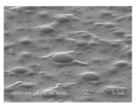
- the non-adhesive layer preferably has a phase separation structure.
- a fine uneven structure can be efficiently formed on the surface of the non-adhesive layer. It is presumed that unevenness is probably generated due to the difference in mass mobility between silicone and (meth) acrylic polymer when the phase separation structure is formed.
- the non-adhesive layer preferably contains a silicone-rich phase containing more silicone than the (meth) acrylic polymer and a (meth) acrylic polymer-rich phase containing more (meth) acrylic polymer than the silicone. More specifically, the non-adhesive layer preferably includes a phase-separated structure in which the silicone-rich phase and the (meth) acrylic polymer-rich phase are independent from each other, and more preferably, the silicone-rich phase is an air interface. It exists on the side (opposite side of the plastic film), and the (meth) acrylic polymer rich phase is present on the plastic film side.
- phase separation structure By having such a phase separation structure, blocking is effectively suppressed by the silicone-rich phase present on the air interface side, and the non-adhesive layer and the plastic film are represented by the (meth) acrylic polymer-rich phase present on the plastic film side.
- the familiarity with and the deformation followability become good.
- phase separation structure can be formed by adjusting the mixing ratio of the silicone and the (meth) acrylic polymer in the non-adhesive layer as follows.
- the non-adhesive layer has a phase-separated structure, and as described above, a silicone-rich phase containing more silicone than (meth) acrylic polymer and a more (meth) acrylic polymer than silicone (meta)
- a silicone-rich phase containing more silicone than (meth) acrylic polymer and a more (meth) acrylic polymer than silicone (meta)
- the inclusion of an acrylic polymer rich phase can be observed by any suitable method.
- an observation method for example, the cross-section of the non-adhesive layer is measured using an electron microscope such as a transmission electron microscope (TEM), a scanning electron microscope (SEM), or a field emission scanning electron microscope (FE-SEM).
- TEM transmission electron microscope
- SEM scanning electron microscope
- FE-SEM field emission scanning electron microscope
- Observation is also made by observing changes in the content of silicon and carbon contained in the composition while changing the probe light depth from the non-adhesive layer air interface side to the inside by infrared absorption spectroscopy using the total reflection method. A method is also mentioned. In addition, a method of observing with an X-ray microanalyzer or X-ray photoelectron spectroscopy is also included. Moreover, you may observe combining these methods suitably.
- silicone: (meth) acrylic polymer 1: 3 to 5: 1.
- the silicone content in the non-adhesive layer is too large, when the film for an adhesive tape or an adhesive tape containing the same is used, followability to deformation such as stretching becomes worse, and the non-adhesive layer is crushed and contaminated. May cause this.
- the content ratio of the (meth) acrylic polymer in the non-adhesive layer is too large, the non-adhesive layer may act as an acrylic adhesive, and blocking may easily occur.
- any appropriate silicone can be adopted as the silicone.
- silicones for example, addition type silicones obtained by forming a peelable film by curing an alkenyl group-containing polydialkylsiloxane and polydialkylhydrogenpolysiloxane by an addition reaction using a platinum compound as a catalyst, a tin-based silicone Examples include a condensation type silicone obtained by reacting a methylol group-containing polydialkylsiloxane and a polydialkylhydrogenpolysiloxane using a catalyst. Examples of the addition type silicone include “KS-776A” and “KS-839L” manufactured by Shin-Etsu Silicone.
- condensation type silicone examples include, for example, “KS723A / B” manufactured by Shin-Etsu Silicone.
- silicone when manufacturing silicone, you may use other crosslinking agents, a crosslinking accelerator, etc. suitably other than a platinum-type catalyst and a tin-type catalyst.
- the properties of silicone are classified into a type dissolved in an organic solvent such as toluene, an emulsion type obtained by emulsifying these, and a solventless type consisting only of silicone.
- silicone / acrylic graft polymer, silicone / acrylic block polymer, and the like can be used.
- silicone / acrylic graft polymer examples include Cymac GS-30, GS101, US-270, US-350, US-380 (above, manufactured by Toagosei Co., Ltd.).
- silicone / acrylic block polymer examples include Modiper FS700, FS710, FS720, FS730, and FS770 (manufactured by NOF Corporation).
- any appropriate (meth) acrylic polymer can be adopted as long as the calculated Tg is 10 ° C. or higher.
- “(meth) acryl” means “acryl and / or methacryl”.
- (Meth) acrylic polymer is a polymer composed of monomer components containing a (meth) acrylic monomer as a main monomer.
- the content of the (meth) acrylic monomer in the monomer component constituting the (meth) acrylic polymer is preferably 50% by weight or more, more preferably 70% by weight to 100% by weight, and still more preferably 90% by weight to 100%. % By weight, particularly preferably from 95% to 100% by weight.
- the monomer in the monomer component may be only one type or two or more types.
- the (meth) acrylic monomer is preferably (meth) acrylic acid ester or (meth) acrylic acid.
- (meth) acrylic acid esters examples include (meth) acrylic acid alkyl esters having 1 to 30 carbon atoms (including cycloalkyl groups), hydroxyl group-containing (meth) acrylic acid esters, and the like. Only one (meth) acrylic acid ester may be used, or two or more may be used.
- Examples of (meth) acrylic acid alkyl esters of alkyl groups having 1 to 30 carbon atoms include, for example, methyl (meth) acrylate, ethyl (meth) acrylate, propyl (meth) acrylate, Isopropyl (meth) acrylate, butyl (meth) acrylate, isobutyl (meth) acrylate, sec-butyl (meth) acrylate, t-butyl (meth) acrylate, pentyl (meth) acrylate, (meth) acrylic Amyl acid, hexyl (meth) acrylate, cyclohexyl (meth) acrylate, heptyl (meth) acrylate, 2-ethylhexyl (meth) acrylate, octyl (meth) acrylate, isooctyl (meth) acrylate, (meth) Nonyl
- (meth) acrylic acid esters preferred are (meth) acrylic acid alkyl esters of alkyl groups having 2 to 20 carbon atoms (including cycloalkyl groups), and more preferred are those having 4 to 18 carbon atoms. (Meth) acrylic acid alkyl ester of an alkyl group (including a cycloalkyl group).
- hydroxyl group-containing (meth) acrylic acid ester examples include 2-hydroxyethyl (meth) acrylate, 2-hydroxypropyl (meth) acrylate, 4-hydroxybutyl (meth) acrylate and the like.
- the monomer component constituting the (meth) acrylic polymer may contain at least one selected from a hydroxyl group-containing monomer and a carboxyl group-containing monomer in order to sufficiently exhibit the effects of the present invention.
- hydroxyl group-containing monomer examples include allyl alcohol. Only one type of hydroxyl group-containing monomer may be used, or two or more types may be used.
- carboxyl group-containing monomer examples include carboxyethyl (meth) acrylate, carboxypentyl (meth) acrylate, crotonic acid, maleic acid, fumaric acid, and itaconic acid. Only one type of carboxyl group-containing monomer may be used, or two or more types may be used.
- the (meth) acrylic polymer in the non-adhesive layer is preferably a monomer component other than the hydroxyl group-containing (meth) acrylic acid ester, with the content ratio of the hydroxyl group-containing (meth) acrylic acid ester in the monomer component constituting it.
- the total amount is preferably 2 to 30% by weight, more preferably 3 to 25% by weight, and particularly preferably 5 to 20% by weight.
- the content ratio of the hydroxyl group-containing (meth) acrylate ester in the monomer component constituting the (meth) acrylic polymer in the non-adhesion layer is based on the total amount of monomer components other than the hydroxyl group-containing (meth) acrylate ester, If it falls within the above range, a minute uneven structure is more efficiently formed on the surface of the non-adhesive layer, and the formation of this uneven structure allows the adhesive tape film of the present invention to be adsorbed and fixed by negative pressure.
- the occurrence of over-adhesion can be further suppressed, blocking in the roll form can be more effectively suppressed, and tearing or tearing when unwinding from the roll form can be further suppressed.
- the (meth) acrylic polymer in the non-adhesive layer is preferably (meth) acrylic acid and / or (meth) acrylic in the monomer component other than the hydroxyl group-containing (meth) acrylic acid ester in the monomer component constituting it. Acid esters can be included.
- the content ratio of (meth) acrylic acid and (meth) acrylic acid ester is (meth) acrylic acid: (meth) acrylic acid ester by weight ratio, preferably 0: 100 to 20:80. More preferably, it is 0: 100 to 10:90, and still more preferably 0: 100 to 5:95.
- the content ratio of (meth) acrylic acid and (meth) acrylic acid ester is within the above range, a fine uneven structure is more efficiently formed on the surface of the non-adhesive layer.
- (Meth) acrylic polymer can be produced by any suitable polymerization method.
- the non-adhesive layer may contain any appropriate additive as long as the effects of the present invention are not impaired.
- additives include catalysts, ultraviolet absorbers, fillers, anti-aging agents, tackifiers, pigments, dyes, and silane coupling agents.
- the non-adhesive layer has a non-adhesive test peel force of preferably less than 1.0 N / 20 mm, more preferably less than 0.5 N / 20 mm, and even more preferably less than 0.2 N / 20 mm.
- a non-adhesive test peel force of the non-adhesive layer is within the above range, it is possible to further suppress the occurrence of over-adhesion when performing adsorption fixation by negative pressure.
- the non-adhesive test peel force of the non-adhesive layer is measured based on the method described below.
- the thickness of the non-adhesive layer is preferably 0.01 ⁇ m to 10 ⁇ m, more preferably 0.1 ⁇ m to 5 ⁇ m, and still more preferably 0.1 ⁇ m to 2 ⁇ m.
- the thickness of the non-adhesive layer is less than 0.01 ⁇ m, blocking tends to occur.
- the thickness of the non-adhesive layer is larger than 10 ⁇ m, the followability to deformation such as stretching may be deteriorated. If the thickness of the non-adhesive layer is less than 0.01 ⁇ m, the effects of the present invention may be difficult to be exhibited or the manufacture may be difficult.
- Examples of the method of forming the non-adhesive layer on one side of the plastic film include a method of forming the non-adhesive layer by applying the material of the non-adhesive layer on one side of the plastic film and drying.
- Examples of the coating method include a method using a bar coater, a gravure coater, a spin coater, a roll coater, a knife coater, an applicator and the like.
- the pressure-sensitive adhesive tape of the present invention includes a pressure-sensitive adhesive layer on the surface of the plastic film of the present invention opposite to the non-stick layer of the plastic film.
- the thickness of the pressure-sensitive adhesive layer is not particularly limited, and is preferably 1.0 ⁇ m to 30 ⁇ m, more preferably 1.0 ⁇ m to 20 ⁇ m, and further preferably 3.0 ⁇ m to 15 ⁇ m.
- the thickness of the pressure-sensitive adhesive layer is less than 1.0 ⁇ m, there is a possibility that sufficient adhesive force cannot be expressed.
- the thickness of the pressure-sensitive adhesive layer is larger than 30 ⁇ m, the adhesive force becomes too large depending on the use, and the adherend may be crushed during peeling or the like.
- any appropriate pressure-sensitive adhesive can be adopted as long as the effects of the present invention are not impaired.
- Examples of the material for the pressure-sensitive adhesive layer include (meth) acrylic polymer; natural rubber; special natural rubber grafted with monomers such as methyl methacrylate; SBS, SBR, SEPS, SIS, SEBS, polybutene, polyisobutene, polyisobutylene, And synthetic rubbers such as butyl rubber.
- (meth) acrylic polymers are preferable in that they have little adhesive residue on the adherend after peeling, have high cohesiveness, and are excellent in transparency.
- the content ratio of the (meth) acrylic polymer in the pressure-sensitive adhesive layer can be appropriately set according to the purpose.
- the (meth) acrylic polymer is a resin composed of monomer components containing a (meth) acrylic monomer as a main monomer.
- the content ratio of the (meth) acrylic monomer in the monomer component constituting the (meth) acrylic polymer is preferably 50% by weight or more, more preferably 70% by weight to 100% by weight, still more preferably 90% by weight or more. It is 100% by weight, particularly preferably 95% by weight to 100% by weight.
- the monomer in the monomer component may be only one type or two or more types.
- the (meth) acrylic monomer is preferably (meth) acrylic acid ester or (meth) acrylic acid.
- (meth) acrylic acid esters examples include (meth) acrylic acid alkyl esters having 1 to 30 carbon atoms (including cycloalkyl groups), hydroxyl group-containing (meth) acrylic acid esters, and the like. Only one (meth) acrylic acid ester may be used, or two or more may be used.
- Examples of (meth) acrylic acid alkyl esters of alkyl groups having 1 to 30 carbon atoms include, for example, methyl (meth) acrylate, ethyl (meth) acrylate, propyl (meth) acrylate, Isopropyl (meth) acrylate, butyl (meth) acrylate, isobutyl (meth) acrylate, sec-butyl (meth) acrylate, t-butyl (meth) acrylate, pentyl (meth) acrylate, (meth) acrylic Amyl acid, hexyl (meth) acrylate, cyclohexyl (meth) acrylate, heptyl (meth) acrylate, 2-ethylhexyl (meth) acrylate, octyl (meth) acrylate, isooctyl (meth) acrylate, (meth) Nonyl
- (meth) acrylic acid esters preferred are (meth) acrylic acid alkyl esters of alkyl groups having 2 to 20 carbon atoms (including cycloalkyl groups), and more preferred are those having 4 to 18 carbon atoms. (Meth) acrylic acid alkyl ester of an alkyl group (including a cycloalkyl group).
- hydroxyl group-containing (meth) acrylic acid ester examples include 2-hydroxyethyl (meth) acrylate, 2-hydroxypropyl (meth) acrylate, 4-hydroxybutyl (meth) acrylate and the like.
- the monomer component constituting the (meth) acrylic polymer preferably contains at least one selected from a hydroxyl group-containing monomer and a carboxyl group-containing monomer in order to sufficiently exhibit the effect as an adhesive. More preferably, it is a carboxyl group-containing monomer.
- the monomer component which comprises the said (meth) acrylic-type polymer may contain acrylonitrile in order to fully express the effect as an adhesive.
- hydroxyl group-containing monomer examples include 2-hydroxyethyl (meth) acrylate, 2-hydroxypropyl (meth) acrylate, 4-hydroxybutyl (meth) acrylate, allyl alcohol, and the like. Only one type of hydroxyl group-containing monomer may be used, or two or more types may be used.
- carboxyl group-containing monomer examples include (meth) acrylic acid, carboxyethyl (meth) acrylate, carboxypentyl (meth) acrylate, crotonic acid, maleic acid, fumaric acid, and itaconic acid. Only one type of carboxyl group-containing monomer may be used, or two or more types may be used.
- the content ratio of the hydroxyl group-containing monomer in the monomer component constituting the (meth) acrylic polymer is preferably from 0.1% by weight to It is 20% by weight, more preferably 0.1% by weight to 10% by weight.
- the content ratio of the carboxyl group-containing monomer in the monomer component constituting the (meth) acrylic polymer is preferably 0.1 wt. % To 20% by weight, more preferably 0.1% to 10% by weight.
- the monomer component constituting the (meth) acrylic polymer contains at least one selected from a hydroxyl group-containing monomer and a carboxyl group-containing monomer
- a crosslinking agent when used, A cross-linking reaction can be efficiently generated, and the effect as an adhesive can be sufficiently exhibited.
- the content ratio of the hydroxyl group-containing monomer in the monomer component constituting the (meth) acrylic polymer and the content ratio of the carboxyl group-containing monomer in the monomer component constituting the (meth) acrylic polymer are within the above range.
- the content ratio of the hydroxyl group-containing monomer in the monomer component constituting the (meth) acrylic polymer and the content ratio of the carboxyl group-containing monomer in the monomer component constituting the (meth) acrylic polymer are more than the above range.
- the amount is too large, the adhesive force becomes too large, and blocking may occur easily. Further, the adherend may be easily crushed during the peeling operation.
- the pressure-sensitive adhesive layer preferably contains a crosslinking agent.
- the content of the cross-linking agent in the pressure-sensitive adhesive layer can be appropriately set according to the purpose, but preferably the main resin component (preferably a (meth) acrylic polymer). On the other hand, it is 0.1 to 20% by weight.
- crosslinking agent examples include an epoxy crosslinking agent, an isocyanate crosslinking agent, a melamine crosslinking agent, a peroxide crosslinking agent, a metal alkoxide crosslinking agent, a metal chelate crosslinking agent, a metal salt crosslinking agent, and a carbodiimide crosslinking.
- melamine-based crosslinking agents, epoxy-based crosslinking agents, and isocyanate-based crosslinking agents are preferable because the effects of the present invention can be sufficiently expressed.
- a crosslinking agent can be suitably selected as needed and may be only 1 type, and 2 or more types of mixed systems may be sufficient as it.
- the pressure-sensitive adhesive layer may contain a plasticizer.
- the content of the plasticizer in the pressure-sensitive adhesive layer can be appropriately set according to the purpose, but is preferably 0.1% by weight to 50% by weight. By keeping the content of the plasticizer in the pressure-sensitive adhesive layer within the above range, the effect of the present invention can be expressed more effectively.
- the content ratio of the plasticizer in the pressure-sensitive adhesive layer is larger than 50% by weight, the pressure-sensitive adhesive layer becomes too flexible, and there is a possibility that adhesive residue and adherend contamination are likely to occur.
- plasticizer examples include phthalate esters, trimellitic acid esters (Dainippon Ink Co., Ltd., W-700, trimellitic acid trioctyl, etc.), adipate esters (manufactured by J-Plus, D620, dioctyl adipate, diisononyl adipate, etc.), phosphate esters (such as tricresyl phosphate), adipic acid esters, citrate esters (such as acetyl citrate tributyl), sebacic acid esters, acceleratoric acid esters, maleic acid esters Benzoic acid ester, polyether polyester, epoxy polyester (epoxidized soybean oil, epoxidized linseed oil, etc.), polyester (low molecular polyester comprising carboxylic acid and glycol, etc.) and the like. In the present invention, it is preferable to use an ester plasticizer. Only one type of plasticizer may be used, or two or more types may be used.
- the pressure-sensitive adhesive layer may contain any appropriate catalyst in order to promote a crosslinking reaction or the like.
- the content of the catalyst in the pressure-sensitive adhesive layer can be appropriately set according to the purpose, but is preferably 0.01% by weight to 10% by weight. By keeping the content ratio of the catalyst in the pressure-sensitive adhesive layer within the above range, the effect of the present invention can be expressed more effectively.
- catalysts examples include tetraisopropyl titanate, tetra-n-butyl titanate, tin octylate, lead octylate, cobalt octylate, zinc octylate, calcium octylate, lead naphthenate, cobalt naphthenate, dibutyltin Organometallic compounds such as acetate, dibutyltin dioctate, dibutyltin dilaurate, dioctyltin dilaurate, dibutyltin maleate; butylamine, dibutylamine, hexylamine, t-butylamine, ethylenediamine, isophoronediamine, imidazole, lithium hydroxide, potassium hydroxide, Basic compounds such as sodium methylate; p-toluenesulfonic acid, trichloroacetic acid, phosphoric acid, monoalkyl phosphoric acid, dial
- the pressure-sensitive adhesive layer preferably has an SP value of 9.0 (cal / cm 3 ) 0.5 to 12.0 (cal / cm 3 ) 0.5 in order to further manifest the effects of the present invention. More preferably, it is 9.5 (cal / cm 3 ) 0.5 to 11.0 (cal / cm 3 ) 0.5 .
- the SP value is a solubility parameter calculated by the Small formula. The SP value can be calculated by a method described in a known document (for example, Journal of Applied Chemistry, 3, 71, 1953., etc.).
- the pressure-sensitive adhesive layer may contain any appropriate additive as long as the effects of the present invention are not impaired.
- additives include ultraviolet absorbers, fillers, anti-aging agents, tackifiers, pigments, dyes, and silane coupling agents.
- the pressure-sensitive adhesive tape of the present invention may have a release liner on the surface of the pressure-sensitive adhesive layer.
- any appropriate separator can be adopted as the release liner.
- a release liner for example, a base material having a release layer such as a plastic film or paper surface-treated with a release agent such as silicone-based, long-chain alkyl-based, fluorine-based, molybdenum sulfide; polytetrafluoroethylene, Low-adhesive substrate made of a fluoropolymer such as polychlorotrifluoroethylene, polyvinyl fluoride, polyvinylidene fluoride, tetrafluoroethylene / hexafluoropropylene copolymer, chlorofluoroethylene / vinylidene fluoride copolymer; And a low-adhesive substrate made of a nonpolar polymer such as a resin (for example, polyethylene, polypropylene, etc.).
- the adhesive tape of the present invention can be used for any appropriate application. Since the pressure-sensitive adhesive tape of the present invention has the film for pressure-sensitive adhesive tapes of the present invention, as described above, overadhesion due to heat generation of the pedestal occurs when dicing or the like is performed by adsorbing and fixing to the fixing pedestal by negative pressure. Can be effectively suppressed, blocking in the roll form is effectively suppressed, and when unrolling from the roll form, it does not tear or tear, and the non-adhesive layer and the plastic film Familiarity is good and followability to deformation such as stretching is good. Therefore, it can be suitably used for semiconductor processing using a semiconductor wafer made of a fragile material and having a fine and fine circuit pattern as an adherend.
- the adhesive tape of the present invention When the adhesive tape of the present invention is used for semiconductor processing, it is possible to effectively suppress the occurrence of over-adhesion due to heat generation or the like of the pedestal when performing dicing or the like by adsorbing and fixing to the pedestal for fixing by negative pressure.
- the semiconductor manufacturing process including dicing can proceed smoothly.
- film deformation and stress strain accumulation caused by blocking conventionally do not occur.
- the stress strain since the stress strain is not released spontaneously after being bonded to the semiconductor wafer, the semiconductor wafer can be effectively prevented from being crushed.
- the wafer used for the LED is made of a very fragile material such as gallium nitride, gallium arsenide, or silicon carbide, the pressure-sensitive adhesive tape of the present invention is very suitable for LED dicing.
- Part means part by weight.
- the amount of the reagent supplied in the solution is represented by the amount of solid content remaining after the solution is volatilized (solid content conversion amount).
- the maximum elongation was measured with an Instron type tensile tester (manufactured by Shimadzu Corporation, Autograph) in accordance with JIS-K-7127. Specifically, after a sample having a width of 20 mm and a length of 100 mm was set at a distance between chucks of 50 mm, the sample was pulled at a pulling speed of 0.3 m / min, and the value at the time of breaking was measured.
- the elastic modulus was measured according to JIS-K-7127.
- ⁇ Arithmetic mean surface roughness Ra> Using a confocal laser microscope “LEXT3000” manufactured by OLYMPUS, measurement was performed in 3D mode with an objective lens of 20 times. The observation range in the 3D mode was determined by setting the positions where the CF image (confocal image) becomes dark when the lens is moved up and down as the observation range Top and Bottom, respectively. As the image capturing method in the 3D mode, image capturing was performed at a pitch of 0.2 ⁇ m by the Step method. Arithmetic mean surface roughness Ra was measured by measuring Ra at an arbitrary place by analysis mode roughness analysis. In addition, the value was calculated
- required by the average value of n 5.
- the slide glass was reciprocated once with a 2 kg roller, and the slide glass and the back surface of the tape-attached slide glass were bonded together. Left for a minute. After being left to cool to room temperature, it was peeled at 0 ° with an Instron type tensile tester (manufactured by Shimadzu Corporation, Autograph) at a tensile speed of 0.3 m / min. The peel force (maximum value) at that time was measured and evaluated according to the following criteria. ⁇ : Peeling force is less than 5.0N. (Triangle
- ⁇ Non-stick test peel strength> Referring to JIS-Z-0237, an adhesive tape film or adhesive tape containing an adherend and a non-adhesive layer is held for 1 hour or more under storage at 23 ° C., and then the non-adhesive surface is applied to SUS430BA at a linear pressure of 8 kg / m, crimping at a crimping speed of 0.3 m / min, and the peeling force after 30 minutes was measured at a tensile speed of 0.3 m / min and 180 ° peel.
- ⁇ 0.5 N / 20 mm or more and less than 1.0 N / 20 mm.
- X 1.0 N / 20 mm or more.
- the pressure-sensitive adhesive layer surface of the pressure-sensitive adhesive tape is pressure-bonded to the outermost surface (back layer) opposite to the pressure-sensitive adhesive layer of the same pressure-sensitive adhesive tape at a linear pressure of 8 kg / m and a pressure bonding speed of 0.3 m / min.
- peeling was performed by a 180 ° peel test at a tensile rate of 0.3 m / min (based on JIS-Z-0237), and the blocking (peeling force) between the pressure-sensitive adhesive layer surface and the back layer was measured.
- the evaluation was made as a comprehensive evaluation by measuring the peeling force, and confirming that the back layer dropped off and the pressure-sensitive adhesive layer was destroyed (cohesive failure, glue residue due to throwing failure). Evaluation was according to the following criteria. ⁇ : Peeling force less than 3.0 N / 20 mm, no visual drop-out, no destruction of the adhesive layer. X: Peeling force is 3.0 N / 20 mm or more, or there is a dropout by visual observation and destruction of the pressure-sensitive adhesive layer.
- Throwing property confirmation test A The adhesive tape film or adhesive tape is stretched to 200% at a tensile speed of 0.3 m / min to 3 m / min, and the outermost side opposite to the adhesive layer of the adhesive tape film or adhesive tape during and after stretching is stretched. The detachability of the outer surface (back layer) was visually evaluated.
- Thowing property confirmation test B After stretching in the same manner as the anchoring property confirmation test A, a NO. 31B manufactured by Nitto Denko Corporation was used as the back treatment layer, and the crimping speed was 0.3 m / min with a 2 kg roller (25 mm width). And then stored at 23 ° C.
- the calculated Tg of the acrylic copolymer was 67.8 ° C., and the SP value was 10.7 (cal / cm 3 ) 0.5 .
- Table 1 Various evaluation results are shown in Table 1. Moreover, when the non-adhesive layer is observed by SEM, as shown in FIGS.
- the composition is different between the air interface side and the plastic film side due to the density of the morphology observation image, Silicone rich phase containing more silicone than (meth) acrylic polymer and (meth) acrylic polymer rich phase containing more than (meth) acrylic polymer than silicone, silicone rich phase and (meth)
- the acrylic polymer-rich phase has a phase separation structure independent of each other, the silicone-rich phase exists on the air interface side (opposite side of the plastic film), and the (meth) acrylic polymer-rich phase is on the plastic film side It was observed that Further, when infrared spectroscopy (ATR-IR) was performed on the non-adhesive layer by a total reflection method, it was found that Si—CH 3 derived from a peak near 1725 cm ⁇ 1 derived from a carbonyl group in the (meth) acrylic polymer phase.
- ATR-IR infrared spectroscopy
- BA butyl acrylate
- AN acrylonitrile
- AA acrylic acid
- melamine-based crosslinking agent butanol-modified melamine formaldehyde resin
- a toluene solution of an adhesive comprising 10 parts by weight of “Super Becamine J-820-60N” (manufactured by Nippon Polyurethane) and 60 parts by weight of a DOP plasticizer (bis (2-ethylhexyl phthalate), manufactured by Jplus) was prepared. .
- Table 1 The calculated Tg of the acrylic copolymer was 80.0 ° C.
- the SP value was 10.4 (cal / cm 3 ) 0.5
- Table 1 Various evaluation results are shown in Table 1.
- Table 1 Various evaluation results are shown in Table 1.
- Table 1 Various evaluation results are shown in Table 1.
- Example 9 As a release liner, a 38 ⁇ m thick PET liner subjected to Si treatment was attached to the pressure-sensitive adhesive layer side of the pressure-sensitive adhesive tape (5) obtained in Example 5 to obtain a pressure-sensitive adhesive tape (9).
- Table 1 Various evaluation results are shown in Table 1.
- Table 1 Various evaluation results are shown in Table 1.
- Table 1 Various evaluation results are shown in Table 1.
- Example 3 In Example 3, except having not formed the non-adhesion layer, it carried out similarly to Example 3 and obtained the adhesive tape (C1). Various evaluation results are shown in Table 1.
- the pressure-sensitive adhesive tape of the present invention has the film for pressure-sensitive adhesive tapes of the present invention, as described above, overadhesion due to heat generation of the pedestal occurs when dicing or the like is performed by adsorbing and fixing to the fixing pedestal by negative pressure. Can be effectively suppressed, blocking in the roll form is effectively suppressed, and when unrolling from the roll form, it does not tear or tear, and the non-adhesive layer and the plastic film Familiarity is good and followability to deformation such as stretching is good. Therefore, it can be suitably used for semiconductor processing using a semiconductor wafer made of a fragile material and having a fine and fine circuit pattern as an adherend.
- the pressure-sensitive adhesive tape of the present invention When the pressure-sensitive adhesive tape of the present invention is used for semiconductor processing, it is possible to suppress the occurrence of over-adhesion when performing suction fixation by negative pressure, and thus the semiconductor manufacturing process including dicing can be smoothly advanced.
- the adhesive tape of the present invention when the adhesive tape of the present invention is used for semiconductor processing, film deformation and stress strain accumulation caused by blocking conventionally do not occur.
- the stress strain since the stress strain is not released spontaneously after being bonded to the semiconductor wafer, the semiconductor wafer can be effectively prevented from being crushed.
- the wafer used for the LED is made of a very fragile material such as gallium nitride, gallium arsenide, or silicon carbide, the pressure-sensitive adhesive tape of the present invention is very suitable for LED dicing.
Landscapes
- Chemical & Material Sciences (AREA)
- Organic Chemistry (AREA)
- Chemical Kinetics & Catalysis (AREA)
- Engineering & Computer Science (AREA)
- Polymers & Plastics (AREA)
- Medicinal Chemistry (AREA)
- Health & Medical Sciences (AREA)
- Condensed Matter Physics & Semiconductors (AREA)
- Microelectronics & Electronic Packaging (AREA)
- Power Engineering (AREA)
- Computer Hardware Design (AREA)
- Manufacturing & Machinery (AREA)
- General Physics & Mathematics (AREA)
- Physics & Mathematics (AREA)
- Adhesive Tapes (AREA)
- Adhesives Or Adhesive Processes (AREA)
- Laminated Bodies (AREA)
Priority Applications (4)
| Application Number | Priority Date | Filing Date | Title |
|---|---|---|---|
| CN201380003304.7A CN103857524B (zh) | 2012-02-28 | 2013-02-08 | 粘合带用薄膜和粘合带 |
| EP13754774.1A EP2722171A4 (en) | 2012-02-28 | 2013-02-08 | FILM FOR ADHESIVE TAPE AND ADHESIVE TAPE |
| KR1020147002629A KR101469428B1 (ko) | 2012-02-28 | 2013-02-08 | 점착 테이프용 필름 및 점착 테이프 |
| US14/237,067 US9460952B2 (en) | 2012-02-28 | 2013-02-08 | Film for pressure-sensitive adhesive tape and pressure-sensitive adhesive tape |
Applications Claiming Priority (2)
| Application Number | Priority Date | Filing Date | Title |
|---|---|---|---|
| JP2012-041172 | 2012-02-28 | ||
| JP2012041172A JP5610642B2 (ja) | 2012-02-28 | 2012-02-28 | 粘着テープ用フィルムおよび粘着テープ |
Publications (1)
| Publication Number | Publication Date |
|---|---|
| WO2013129080A1 true WO2013129080A1 (ja) | 2013-09-06 |
Family
ID=49082282
Family Applications (1)
| Application Number | Title | Priority Date | Filing Date |
|---|---|---|---|
| PCT/JP2013/053015 WO2013129080A1 (ja) | 2012-02-28 | 2013-02-08 | 粘着テープ用フィルムおよび粘着テープ |
Country Status (7)
Cited By (5)
| Publication number | Priority date | Publication date | Assignee | Title |
|---|---|---|---|---|
| EP2918632A1 (en) * | 2014-03-11 | 2015-09-16 | Nitto Denko Corporation | Pressure-sensitive adhesive tape |
| CN108271381A (zh) * | 2016-03-04 | 2018-07-10 | 琳得科株式会社 | 半导体加工用片 |
| WO2019107544A1 (ja) * | 2017-11-30 | 2019-06-06 | 三菱ケミカル株式会社 | 離型フィルム及び積層体の製造方法 |
| JP2019098748A (ja) * | 2017-11-30 | 2019-06-24 | 三菱ケミカル株式会社 | 離型フィルム |
| WO2020105312A1 (ja) * | 2018-11-22 | 2020-05-28 | Tdk株式会社 | はく離フィルム、セラミック部品シート、はく離フィルムの製造方法、セラミック部品シートの製造方法、及び積層セラミックコンデンサの製造方法 |
Families Citing this family (10)
| Publication number | Priority date | Publication date | Assignee | Title |
|---|---|---|---|---|
| JP6071712B2 (ja) * | 2013-04-05 | 2017-02-01 | 日東電工株式会社 | 粘着テープ |
| CN104130724B (zh) * | 2014-07-23 | 2016-04-20 | 日东电工(上海松江)有限公司 | 氯乙烯系胶粘片和胶带 |
| JP6404787B2 (ja) * | 2014-09-26 | 2018-10-17 | 信越化学工業株式会社 | ウエハ加工体、ウエハ加工用仮接着材、及び薄型ウエハの製造方法 |
| JP6513371B2 (ja) * | 2014-11-06 | 2019-05-15 | 日東電工株式会社 | 表面保護シート |
| JP2017132940A (ja) * | 2016-01-29 | 2017-08-03 | 日東電工株式会社 | 粘着テープ |
| WO2017150018A1 (ja) * | 2016-02-29 | 2017-09-08 | リンテック株式会社 | 半導体加工シート |
| JP6837879B2 (ja) * | 2016-08-26 | 2021-03-03 | 日東電工株式会社 | 粘着テープ |
| US12109789B2 (en) * | 2017-12-26 | 2024-10-08 | Cytec Industries Inc. | Self-releasing, UV blocking surfacing materials for composite parts |
| JP6749464B1 (ja) * | 2019-03-20 | 2020-09-02 | 積水化学工業株式会社 | 粘着テープ及び粘着テープロール |
| JP6793895B1 (ja) * | 2019-04-16 | 2020-12-02 | 信越化学工業株式会社 | ペリクル用粘着剤、ペリクル、ペリクル付露光原版、半導体装置の製造方法、液晶表示板の製造方法、露光原版の再生方法及び剥離残渣低減方法 |
Citations (7)
| Publication number | Priority date | Publication date | Assignee | Title |
|---|---|---|---|---|
| JPH08197688A (ja) * | 1995-01-24 | 1996-08-06 | Teijin Ltd | 積層フイルム |
| JP2004210823A (ja) * | 2002-12-26 | 2004-07-29 | Asahi Kasei Chemicals Corp | 粘着テープ |
| JP2008031196A (ja) * | 2006-07-26 | 2008-02-14 | Nitto Denko Corp | 金属箔粘着テープおよび冷蔵庫 |
| WO2009028069A1 (ja) | 2007-08-30 | 2009-03-05 | Defacto Corp. | コンテンツの提供制御方法、装置、およびシステム |
| JP2009239124A (ja) | 2008-03-27 | 2009-10-15 | Furukawa Electric Co Ltd:The | ウェハ表面保護テープ |
| JP2010201836A (ja) | 2009-03-05 | 2010-09-16 | Oji Paper Co Ltd | テープ糊用両面離型フィルム |
| JP2012245746A (ja) * | 2011-05-30 | 2012-12-13 | Iwao Kk | 離型性シート部材 |
Family Cites Families (20)
| Publication number | Priority date | Publication date | Assignee | Title |
|---|---|---|---|---|
| US5154974A (en) * | 1986-06-23 | 1992-10-13 | Norman Alfred W | Adhesive composition having improved cutting properties |
| DE68905827T2 (de) * | 1988-01-18 | 1993-07-08 | Nitto Denko Corp | Trennmittel und verbundwerkstoff mit vulkanisierter trennmittelschicht. |
| TW496881B (en) * | 1997-05-13 | 2002-08-01 | Teijin Ltd | Release film |
| JP3599158B2 (ja) * | 1997-12-12 | 2004-12-08 | 王子製紙株式会社 | 粘着テープ |
| US6541109B1 (en) * | 1999-10-08 | 2003-04-01 | 3M Innovative Properties Company | Release coating formulation providing low adhesion release surfaces for pressure sensitive adhesives |
| JP4747420B2 (ja) * | 2001-02-09 | 2011-08-17 | 王子製紙株式会社 | 熱転写記録可能な剥離シート及び粘着テープ |
| US6828018B2 (en) * | 2001-05-29 | 2004-12-07 | Cmc Daymark Corporation | Water dissolvable tape |
| US20050003216A1 (en) * | 2003-06-30 | 2005-01-06 | Jean-Marc Frances | Microparticle containing silicone release coatings having improved anti-block and release properties |
| JP2008197320A (ja) | 2007-02-13 | 2008-08-28 | Nippon Paint Co Ltd | 防眩性コーティング組成物、防眩フィルムおよびその製造方法 |
| KR20100075442A (ko) * | 2007-08-30 | 2010-07-02 | 덴끼 가가꾸 고교 가부시키가이샤 | 점착 시트 및 전자 부품의 제조 방법 |
| MY150038A (en) * | 2007-09-19 | 2013-11-29 | Toray Industries | Adhesive composition for electronic components, and adhesive sheet for electronic components using the same |
| JP2009256609A (ja) * | 2008-03-28 | 2009-11-05 | Lintec Corp | 粘着シート及びその製造方法 |
| DE102009054322A1 (de) * | 2009-11-24 | 2011-05-26 | Huhtamaki Forchheim Zweigniederlassung Der Huhtamaki Deutschland Gmbh & Co. Kg | Trennfolie mit Schaumstruktur |
| JP5482368B2 (ja) * | 2010-03-29 | 2014-05-07 | Tdk株式会社 | 剥離フィルム |
| JP5391158B2 (ja) * | 2010-06-30 | 2014-01-15 | 古河電気工業株式会社 | ウエハ貼着用粘着シートおよびそれを用いたウエハの加工方法 |
| DE102011117831A1 (de) * | 2011-02-15 | 2012-08-16 | Huhtamaki Forchheim Zweigniederlassung Der Huhtamaki Deutschland Gmbh & Co. Kg | Trennfolie mit rauher Oberflächenstruktur |
| JP6075832B2 (ja) * | 2011-10-17 | 2017-02-08 | 日東電工株式会社 | 粘着テープ用フィルムおよび粘着テープ |
| JP5978051B2 (ja) * | 2011-10-17 | 2016-08-24 | 日東電工株式会社 | 粘着テープ用フィルムおよび粘着テープ |
| JP5946290B2 (ja) * | 2012-02-28 | 2016-07-06 | 日東電工株式会社 | 粘着テープ用フィルムおよび粘着テープ |
| JP6005952B2 (ja) * | 2012-02-28 | 2016-10-12 | 日東電工株式会社 | 粘着テープ用フィルムおよび粘着テープ |
-
2012
- 2012-02-28 JP JP2012041172A patent/JP5610642B2/ja active Active
-
2013
- 2013-02-08 CN CN201380003304.7A patent/CN103857524B/zh active Active
- 2013-02-08 KR KR1020147002629A patent/KR101469428B1/ko active Active
- 2013-02-08 EP EP13754774.1A patent/EP2722171A4/en not_active Withdrawn
- 2013-02-08 EP EP17002013.5A patent/EP3326808A1/en not_active Withdrawn
- 2013-02-08 US US14/237,067 patent/US9460952B2/en not_active Expired - Fee Related
- 2013-02-08 WO PCT/JP2013/053015 patent/WO2013129080A1/ja active Application Filing
- 2013-02-25 TW TW102106581A patent/TWI567156B/zh active
Patent Citations (7)
| Publication number | Priority date | Publication date | Assignee | Title |
|---|---|---|---|---|
| JPH08197688A (ja) * | 1995-01-24 | 1996-08-06 | Teijin Ltd | 積層フイルム |
| JP2004210823A (ja) * | 2002-12-26 | 2004-07-29 | Asahi Kasei Chemicals Corp | 粘着テープ |
| JP2008031196A (ja) * | 2006-07-26 | 2008-02-14 | Nitto Denko Corp | 金属箔粘着テープおよび冷蔵庫 |
| WO2009028069A1 (ja) | 2007-08-30 | 2009-03-05 | Defacto Corp. | コンテンツの提供制御方法、装置、およびシステム |
| JP2009239124A (ja) | 2008-03-27 | 2009-10-15 | Furukawa Electric Co Ltd:The | ウェハ表面保護テープ |
| JP2010201836A (ja) | 2009-03-05 | 2010-09-16 | Oji Paper Co Ltd | テープ糊用両面離型フィルム |
| JP2012245746A (ja) * | 2011-05-30 | 2012-12-13 | Iwao Kk | 離型性シート部材 |
Non-Patent Citations (3)
| Title |
|---|
| "Polymer Handbook", 1989, AWILEY- INTERSCIENCE PUBLICATION |
| JOURNAL OF APPLIED CHEMISTRY, vol. 3, 1953, pages 71 |
| See also references of EP2722171A4 |
Cited By (12)
| Publication number | Priority date | Publication date | Assignee | Title |
|---|---|---|---|---|
| EP2918632A1 (en) * | 2014-03-11 | 2015-09-16 | Nitto Denko Corporation | Pressure-sensitive adhesive tape |
| US9834706B2 (en) | 2014-03-11 | 2017-12-05 | Nitto Denko Corporation | Pressure-sensitive adhesive tape |
| CN108271381A (zh) * | 2016-03-04 | 2018-07-10 | 琳得科株式会社 | 半导体加工用片 |
| WO2019107544A1 (ja) * | 2017-11-30 | 2019-06-06 | 三菱ケミカル株式会社 | 離型フィルム及び積層体の製造方法 |
| JP2019098748A (ja) * | 2017-11-30 | 2019-06-24 | 三菱ケミカル株式会社 | 離型フィルム |
| JP7188029B2 (ja) | 2017-11-30 | 2022-12-13 | 三菱ケミカル株式会社 | 離型フィルム |
| US11673295B2 (en) | 2017-11-30 | 2023-06-13 | Mitsubishi Chemical Corporation | Mold release film and method for producing laminate |
| US11724423B2 (en) | 2017-11-30 | 2023-08-15 | Mitsubishi Chemical Corporation | Mold release film and method for producing laminate |
| WO2020105312A1 (ja) * | 2018-11-22 | 2020-05-28 | Tdk株式会社 | はく離フィルム、セラミック部品シート、はく離フィルムの製造方法、セラミック部品シートの製造方法、及び積層セラミックコンデンサの製造方法 |
| JPWO2020105312A1 (ja) * | 2018-11-22 | 2021-02-15 | Tdk株式会社 | はく離フィルム、セラミック部品シート、はく離フィルムの製造方法、セラミック部品シートの製造方法、及び積層セラミックコンデンサの製造方法 |
| JP2021176704A (ja) * | 2018-11-22 | 2021-11-11 | Tdk株式会社 | はく離フィルム、セラミック部品シート、はく離フィルムの製造方法、セラミック部品シートの製造方法、及び積層セラミックコンデンサの製造方法 |
| JP7435557B2 (ja) | 2018-11-22 | 2024-02-21 | Tdk株式会社 | はく離フィルム、セラミック部品シート、及び積層セラミックコンデンサの製造方法 |
Also Published As
| Publication number | Publication date |
|---|---|
| TW201343856A (zh) | 2013-11-01 |
| CN103857524B (zh) | 2016-04-13 |
| KR20140026648A (ko) | 2014-03-05 |
| EP2722171A1 (en) | 2014-04-23 |
| CN103857524A (zh) | 2014-06-11 |
| JP5610642B2 (ja) | 2014-10-22 |
| US20140178620A1 (en) | 2014-06-26 |
| EP2722171A4 (en) | 2014-12-10 |
| TWI567156B (zh) | 2017-01-21 |
| KR101469428B1 (ko) | 2014-12-04 |
| JP2013176861A (ja) | 2013-09-09 |
| EP3326808A1 (en) | 2018-05-30 |
| US9460952B2 (en) | 2016-10-04 |
Similar Documents
| Publication | Publication Date | Title |
|---|---|---|
| JP5610642B2 (ja) | 粘着テープ用フィルムおよび粘着テープ | |
| JP6005952B2 (ja) | 粘着テープ用フィルムおよび粘着テープ | |
| JP6071712B2 (ja) | 粘着テープ | |
| JP6095996B2 (ja) | 粘着テープ | |
| JP6021263B2 (ja) | 粘着テープ | |
| KR102032066B1 (ko) | 점착 테이프용 필름 및 점착 테이프 | |
| KR101920086B1 (ko) | 점착 테이프용 필름 및 점착 테이프 | |
| JP6075832B2 (ja) | 粘着テープ用フィルムおよび粘着テープ | |
| JP5946289B2 (ja) | 粘着テープ用フィルムおよび粘着テープ | |
| JP5946290B2 (ja) | 粘着テープ用フィルムおよび粘着テープ | |
| CN103045115B (zh) | 压敏胶粘带用膜和压敏胶粘带 |
Legal Events
| Date | Code | Title | Description |
|---|---|---|---|
| 121 | Ep: the epo has been informed by wipo that ep was designated in this application |
Ref document number: 13754774 Country of ref document: EP Kind code of ref document: A1 |
|
| ENP | Entry into the national phase |
Ref document number: 20147002629 Country of ref document: KR Kind code of ref document: A |
|
| WWE | Wipo information: entry into national phase |
Ref document number: 14237067 Country of ref document: US |
|
| NENP | Non-entry into the national phase |
Ref country code: DE |