WO2013125501A1 - 導光体ユニット及びイメージセンサ - Google Patents
導光体ユニット及びイメージセンサ Download PDFInfo
- Publication number
- WO2013125501A1 WO2013125501A1 PCT/JP2013/053924 JP2013053924W WO2013125501A1 WO 2013125501 A1 WO2013125501 A1 WO 2013125501A1 JP 2013053924 W JP2013053924 W JP 2013053924W WO 2013125501 A1 WO2013125501 A1 WO 2013125501A1
- Authority
- WO
- WIPO (PCT)
- Prior art keywords
- light guide
- light
- face
- positioning
- guide unit
- Prior art date
- Legal status (The legal status is an assumption and is not a legal conclusion. Google has not performed a legal analysis and makes no representation as to the accuracy of the status listed.)
- Ceased
Links
Images


Classifications
-
- G—PHYSICS
- G02—OPTICS
- G02B—OPTICAL ELEMENTS, SYSTEMS OR APPARATUS
- G02B6/00—Light guides; Structural details of arrangements comprising light guides and other optical elements, e.g. couplings
- G02B6/0001—Light guides; Structural details of arrangements comprising light guides and other optical elements, e.g. couplings specially adapted for lighting devices or systems
- G02B6/0011—Light guides; Structural details of arrangements comprising light guides and other optical elements, e.g. couplings specially adapted for lighting devices or systems the light guides being planar or of plate-like form
- G02B6/0013—Means for improving the coupling-in of light from the light source into the light guide
- G02B6/0015—Means for improving the coupling-in of light from the light source into the light guide provided on the surface of the light guide or in the bulk of it
- G02B6/0016—Grooves, prisms, gratings, scattering particles or rough surfaces
-
- H—ELECTRICITY
- H04—ELECTRIC COMMUNICATION TECHNIQUE
- H04N—PICTORIAL COMMUNICATION, e.g. TELEVISION
- H04N1/00—Scanning, transmission or reproduction of documents or the like, e.g. facsimile transmission; Details thereof
- H04N1/024—Details of scanning heads ; Means for illuminating the original
- H04N1/0249—Arrangements for mounting or supporting elements within a scanning head
-
- H—ELECTRICITY
- H04—ELECTRIC COMMUNICATION TECHNIQUE
- H04N—PICTORIAL COMMUNICATION, e.g. TELEVISION
- H04N1/00—Scanning, transmission or reproduction of documents or the like, e.g. facsimile transmission; Details thereof
- H04N1/024—Details of scanning heads ; Means for illuminating the original
- H04N1/028—Details of scanning heads ; Means for illuminating the original for picture information pick-up
- H04N1/02815—Means for illuminating the original, not specific to a particular type of pick-up head
- H04N1/0282—Using a single or a few point light sources, e.g. a laser diode
- H04N1/02835—Using a single or a few point light sources, e.g. a laser diode in combination with a light guide, e.g. optical fibre, glass plate
-
- H—ELECTRICITY
- H04—ELECTRIC COMMUNICATION TECHNIQUE
- H04N—PICTORIAL COMMUNICATION, e.g. TELEVISION
- H04N1/00—Scanning, transmission or reproduction of documents or the like, e.g. facsimile transmission; Details thereof
- H04N1/024—Details of scanning heads ; Means for illuminating the original
- H04N1/028—Details of scanning heads ; Means for illuminating the original for picture information pick-up
- H04N1/02815—Means for illuminating the original, not specific to a particular type of pick-up head
- H04N1/02885—Means for compensating spatially uneven illumination, e.g. an aperture arrangement
- H04N1/0289—Light diffusing elements, e.g. plates or filters
-
- H—ELECTRICITY
- H04—ELECTRIC COMMUNICATION TECHNIQUE
- H04N—PICTORIAL COMMUNICATION, e.g. TELEVISION
- H04N1/00—Scanning, transmission or reproduction of documents or the like, e.g. facsimile transmission; Details thereof
- H04N1/024—Details of scanning heads ; Means for illuminating the original
- H04N1/028—Details of scanning heads ; Means for illuminating the original for picture information pick-up
- H04N1/03—Details of scanning heads ; Means for illuminating the original for picture information pick-up with photodetectors arranged in a substantially linear array
- H04N1/031—Details of scanning heads ; Means for illuminating the original for picture information pick-up with photodetectors arranged in a substantially linear array the photodetectors having a one-to-one and optically positive correspondence with the scanned picture elements, e.g. linear contact sensors
- H04N1/0318—Integral pick-up heads, i.e. self-contained heads whose basic elements are a light-source, a lens array and a photodetector array which are supported by a single-piece frame
-
- H—ELECTRICITY
- H10—SEMICONDUCTOR DEVICES; ELECTRIC SOLID-STATE DEVICES NOT OTHERWISE PROVIDED FOR
- H10F—INORGANIC SEMICONDUCTOR DEVICES SENSITIVE TO INFRARED RADIATION, LIGHT, ELECTROMAGNETIC RADIATION OF SHORTER WAVELENGTH OR CORPUSCULAR RADIATION
- H10F39/00—Integrated devices, or assemblies of multiple devices, comprising at least one element covered by group H10F30/00, e.g. radiation detectors comprising photodiode arrays
- H10F39/80—Constructional details of image sensors
- H10F39/806—Optical elements or arrangements associated with the image sensors
-
- H—ELECTRICITY
- H04—ELECTRIC COMMUNICATION TECHNIQUE
- H04N—PICTORIAL COMMUNICATION, e.g. TELEVISION
- H04N2201/00—Indexing scheme relating to scanning, transmission or reproduction of documents or the like, and to details thereof
- H04N2201/024—Indexing scheme relating to scanning, transmission or reproduction of documents or the like, and to details thereof deleted
- H04N2201/02452—Arrangements for mounting or supporting elements within a scanning head
- H04N2201/02454—Element mounted or supported
- H04N2201/02462—Illuminating means
-
- H—ELECTRICITY
- H04—ELECTRIC COMMUNICATION TECHNIQUE
- H04N—PICTORIAL COMMUNICATION, e.g. TELEVISION
- H04N2201/00—Indexing scheme relating to scanning, transmission or reproduction of documents or the like, and to details thereof
- H04N2201/024—Indexing scheme relating to scanning, transmission or reproduction of documents or the like, and to details thereof deleted
- H04N2201/02452—Arrangements for mounting or supporting elements within a scanning head
- H04N2201/02466—Mounting or supporting method
- H04N2201/02472—Mounting or supporting method using clips
-
- H—ELECTRICITY
- H04—ELECTRIC COMMUNICATION TECHNIQUE
- H04N—PICTORIAL COMMUNICATION, e.g. TELEVISION
- H04N2201/00—Indexing scheme relating to scanning, transmission or reproduction of documents or the like, and to details thereof
- H04N2201/024—Indexing scheme relating to scanning, transmission or reproduction of documents or the like, and to details thereof deleted
- H04N2201/028—Indexing scheme relating to scanning, transmission or reproduction of documents or the like, and to details thereof deleted for picture information pick-up
- H04N2201/03—Indexing scheme relating to scanning, transmission or reproduction of documents or the like, and to details thereof deleted for picture information pick-up deleted
- H04N2201/031—Indexing scheme relating to scanning, transmission or reproduction of documents or the like, and to details thereof deleted for picture information pick-up deleted deleted
- H04N2201/03104—Integral pick-up heads, i.e. self-contained heads whose basic elements are a light source, a lens and a photodetector supported by a single-piece frame
- H04N2201/03108—Components of integral heads
- H04N2201/03112—Light source
-
- H—ELECTRICITY
- H04—ELECTRIC COMMUNICATION TECHNIQUE
- H04N—PICTORIAL COMMUNICATION, e.g. TELEVISION
- H04N2201/00—Indexing scheme relating to scanning, transmission or reproduction of documents or the like, and to details thereof
- H04N2201/024—Indexing scheme relating to scanning, transmission or reproduction of documents or the like, and to details thereof deleted
- H04N2201/028—Indexing scheme relating to scanning, transmission or reproduction of documents or the like, and to details thereof deleted for picture information pick-up
- H04N2201/03—Indexing scheme relating to scanning, transmission or reproduction of documents or the like, and to details thereof deleted for picture information pick-up deleted
- H04N2201/031—Indexing scheme relating to scanning, transmission or reproduction of documents or the like, and to details thereof deleted for picture information pick-up deleted deleted
- H04N2201/03104—Integral pick-up heads, i.e. self-contained heads whose basic elements are a light source, a lens and a photodetector supported by a single-piece frame
- H04N2201/03108—Components of integral heads
- H04N2201/03125—Light guide upstream of the scanned picture elements
-
- H—ELECTRICITY
- H04—ELECTRIC COMMUNICATION TECHNIQUE
- H04N—PICTORIAL COMMUNICATION, e.g. TELEVISION
- H04N2201/00—Indexing scheme relating to scanning, transmission or reproduction of documents or the like, and to details thereof
- H04N2201/024—Indexing scheme relating to scanning, transmission or reproduction of documents or the like, and to details thereof deleted
- H04N2201/028—Indexing scheme relating to scanning, transmission or reproduction of documents or the like, and to details thereof deleted for picture information pick-up
- H04N2201/03—Indexing scheme relating to scanning, transmission or reproduction of documents or the like, and to details thereof deleted for picture information pick-up deleted
- H04N2201/031—Indexing scheme relating to scanning, transmission or reproduction of documents or the like, and to details thereof deleted for picture information pick-up deleted deleted
- H04N2201/03104—Integral pick-up heads, i.e. self-contained heads whose basic elements are a light source, a lens and a photodetector supported by a single-piece frame
- H04N2201/03108—Components of integral heads
- H04N2201/03133—Window, i.e. a transparent member mounted in the frame
-
- H—ELECTRICITY
- H04—ELECTRIC COMMUNICATION TECHNIQUE
- H04N—PICTORIAL COMMUNICATION, e.g. TELEVISION
- H04N2201/00—Indexing scheme relating to scanning, transmission or reproduction of documents or the like, and to details thereof
- H04N2201/024—Indexing scheme relating to scanning, transmission or reproduction of documents or the like, and to details thereof deleted
- H04N2201/028—Indexing scheme relating to scanning, transmission or reproduction of documents or the like, and to details thereof deleted for picture information pick-up
- H04N2201/03—Indexing scheme relating to scanning, transmission or reproduction of documents or the like, and to details thereof deleted for picture information pick-up deleted
- H04N2201/031—Indexing scheme relating to scanning, transmission or reproduction of documents or the like, and to details thereof deleted for picture information pick-up deleted deleted
- H04N2201/03104—Integral pick-up heads, i.e. self-contained heads whose basic elements are a light source, a lens and a photodetector supported by a single-piece frame
- H04N2201/03108—Components of integral heads
- H04N2201/03141—Photodetector lens
-
- H—ELECTRICITY
- H04—ELECTRIC COMMUNICATION TECHNIQUE
- H04N—PICTORIAL COMMUNICATION, e.g. TELEVISION
- H04N2201/00—Indexing scheme relating to scanning, transmission or reproduction of documents or the like, and to details thereof
- H04N2201/024—Indexing scheme relating to scanning, transmission or reproduction of documents or the like, and to details thereof deleted
- H04N2201/028—Indexing scheme relating to scanning, transmission or reproduction of documents or the like, and to details thereof deleted for picture information pick-up
- H04N2201/03—Indexing scheme relating to scanning, transmission or reproduction of documents or the like, and to details thereof deleted for picture information pick-up deleted
- H04N2201/031—Indexing scheme relating to scanning, transmission or reproduction of documents or the like, and to details thereof deleted for picture information pick-up deleted deleted
- H04N2201/03104—Integral pick-up heads, i.e. self-contained heads whose basic elements are a light source, a lens and a photodetector supported by a single-piece frame
- H04N2201/03108—Components of integral heads
- H04N2201/03145—Photodetector
Definitions
- the present invention relates to a light guide unit and an image sensor.
- the contact image sensor used in equipment has a light guide.
- the light guide converts light from the light source into linear light extending in the main scanning direction of the document surface.
- Some light guides are cylindrical.
- the cylindrical light guide is disposed such that its longitudinal direction (side surface) faces the main scanning direction of the document surface. Light from the light source enters the light guide from the end face of the light guide and exits from the exit portion on the side surface of the light guide. The light emitted from the light guide becomes light extending in the main scanning direction and illuminates the document surface.
- the light guide is formed by extrusion molding using a transparent resin such as acrylic or polycarbonate as a raw material, it tends to bend and deform. For this reason, it is difficult to manufacture a light guide having a certain length or more.
- the present invention has been made in view of such circumstances, and an object thereof is to provide a light guide unit and an image sensor that can illuminate the main scanning direction of the document surface uniformly with a simple configuration. .
- a light guide unit emits light incident on one end surface from the other end surface and a light emitting portion on a side surface connecting the one end surface and the other end surface.
- a columnar second light guide that is emitted from a light emitting portion and formed so that the one end face is in close contact with the other end face of the first light guide, and formed on the first light guide
- the first positioning portion, the other end surface of the first light guide and the one end surface of the second light guide are in close contact with each other, and the light emitting portion of the first light guide
- the second side surface and the side surface having the light emitting part of the second light guide are flush with each other and engage with the first positioning part. Comprising a second positioning portion formed in the light guide body.
- FIG. 4 is a cross-sectional view taken along the line II-II in FIG. It is a front view of the edge part of the 1st light guide which concerns on Embodiment 1 of this invention. It is a right view of the edge part of the 1st light guide which concerns on Embodiment 1 of this invention. It is a left view of the edge part of the 2nd light guide which concerns on Embodiment 1 of this invention.
- the contact image sensor 10 includes a frame 11, a transmissive body 12, a lighting device 15, a rod lens array 30, a sensor IC 40, and a sensor substrate 50. ing.
- the frame 11 (accommodating portion) is a housing that supports the transmissive body 12 and accommodates the illumination device 15, the rod lens array 30, the sensor IC 40, and the sensor substrate 50.
- the transmissive body 12 is a platen for the original M, and is a transparent plate member that transmits light formed of plastic or glass.
- the illuminating device 15 is a device that emits light from a light emitting portion of a light guide, which will be described later, toward the transmissive body 12 as indicated by a broken line arrow in FIG.
- the light is emitted in the reading width direction of the document M, that is, in the main scanning direction which is the X-axis direction in FIG.
- the rod lens array 30 is composed of a lens body that converges the light reflected from the document M.
- the sensor IC 40 is formed of a light receiving element that receives light converged by the rod lens array 30 and performs photoelectric conversion.
- a plurality of sensor ICs 40 are linearly arranged in the main scanning direction which is the X-axis direction in FIG.
- the sensor substrate 50 is a substrate on which the sensor IC 40 is mounted. The sensor substrate 50 outputs an image signal to the outside.
- the illumination device 15 includes a light guide unit 20, a light emitting diode unit 25, and a holder 29.
- the light guide unit 20 includes a first light guide 21, a second light guide 22, and a third light guide 23.
- the 1st light guide 21, the 2nd light guide 22, and the 3rd light guide 23 are formed from transparent resin, such as acrylic and polycarbonate, for example.
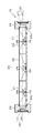
- the 1st light guide 21, the 2nd light guide 22, and the 3rd light guide 23 are cylindrical members which have an equal diameter.
- the first light guide body 21, the second light guide body 22, and the third light guide body 23 are arranged in series so that the respective central axes C1 coincide with each other and the side surfaces thereof are flush with each other. Yes.
- the side surfaces of the first light guide 21, the second light guide 22, and the third light guide 23 of the light guide unit 20 are provided with light guides.
- the light diffusion layer 24 is formed so as to be in a line over the direction of the central axis C1.
- the light diffusion layer 24 is, for example, a coating film formed by applying white ink or the like on the surface of the light guide.
- the light emitted from the light emitting diode unit 25 enters the end of the light guide unit 20.
- the incident light attenuates as the distance from the end of the light guide unit 20 increases. Therefore, the light diffusion layer 24 is installed so that light is emitted uniformly from the light emitting portion of the light guide unit 20.
- the light diffusion layer 24 can be arranged with a gap near the end of the light guide unit 20 and with a narrow gap near the center. Further, the area of the light diffusion layer 24 can be increased from the end toward the center.
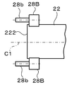
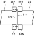
- the first light guide 21 has a pair of first fitting members 28 ⁇ / b> A and 28 ⁇ / b> A on the side surface in the vicinity of the end surface 211 on the side in contact (contact) with the second light guide 22. It has.
- the pair of first fitting members 28A and 28A serve as positioning means (first positioning portions).
- the pair of first fitting members 28 ⁇ / b> A and 28 ⁇ / b> A are fixed to the side surface of the first light guide 21 with an adhesive or the like.
- the first fitting members 28A and 28A are installed at positions symmetrical with respect to the central axis C1.
- the first fitting member 28A is a substantially rectangular parallelepiped member that is formed in a concave shape so that one surface corresponds to the side surface shape of the first light guide 21.
- the first fitting member 28A has a circular through hole 28a.
- the through hole 28 a is formed so that the central axis C 2 of the through hole 28 a is in the same direction as the central axis C 1 of the first light guide 21.
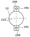
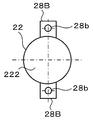
- the second light guide 22 includes a pair of second fitting members 28 ⁇ / b> B and 28 ⁇ / b> B on the side surface in the vicinity of the end surface 222 on the side in contact (close contact) with the first light guide 21. ing.
- the pair of second fitting members 28B and 28B serve as positioning means (second positioning portions).
- the pair of second fitting members 28 ⁇ / b> B and 28 ⁇ / b> B are fixed to the side surface of the second light guide 22 with an adhesive or the like.
- the second fitting members 28B and 28B are disposed at positions symmetrical with respect to the central axis C1.
- the second fitting member 28B is a substantially rectangular parallelepiped member that is formed in a concave shape so that one surface thereof corresponds to the side surface shape of the second light guide 22.
- the second fitting member 28 ⁇ / b> B has a columnar fitting portion 28 b formed with substantially the same diameter as the through hole 28 a of the first light guide 21.
- the fitting portion 28b is disposed so that the central axis C3 of the fitting portion 28b is in the same direction as the central axis C1 of the second light guide 22.
- the distance between the center axis C3 of the fitting portion 28b and the center axis C1 of the second light guide 22 is the center axis of the through hole 28a of the first fitting member 28A disposed in the first light guide 21.
- the distance between C2 and the central axis C1 of the first light guide 21 is the same.
- the second light guide 22 is further provided with a pair of first fitting members 28 ⁇ / b> A on the side surface in the vicinity of the surface 221 on the side in contact (contact) with the third light guide 23. , 28A.
- the pair of first fitting members 28 ⁇ / b> A and 28 ⁇ / b> A are fixed to the side surface of the second light guide 22 with an adhesive or the like.
- the first fitting members 28A and 28A are installed at positions symmetrical with respect to the central axis C1.
- the third light guide 23 includes a pair of second fitting members 28B and 28B on the side surface in the vicinity of the end surface 232 on the side in contact (contact) with the second light guide 22.
- the pair of second fitting members 28 ⁇ / b> B and 28 ⁇ / b> B are fixed to the side surface of the third light guide 23 with an adhesive or the like.
- the second fitting members 28B and 28B are installed at positions symmetrical with respect to the central axis C1.
- the pair of first fitting members 28 ⁇ / b> A and 28 ⁇ / b> A and the second fitting members 28 ⁇ / b> B and 28 ⁇ / b> B disposed on the second light guide 22 are light diffusion layers 24 on the side surfaces of the second light guide 22. For example, it is fixed at a position different from the center axis C1 by 90 degrees, for example.
- the pair of first fitting members 28A and 28A disposed on the first light guide 21 and the pair of second fitting members 28B and 28B disposed on the third light guide 23 are also described. It is the same. In this way, it is possible to prevent the emission of light from each light guide.
- the light emitting diode unit 25 is a light source in which a light emitting diode 27 is mounted on a substrate 26.
- the holder 29 has a through hole 29a.
- the holder 29 supports the end of the light guide unit 20 through one opening of the through hole 29a. In this way, the light emitted from the light emitting diode 27 is reliably incident on the end of the light guide unit 20.
- the holder 29 supports the light emitting diode unit 25 at the other opening.
- the illumination device 15 includes the first light guide 21, the second light guide 22, the third light guide 23, the light emitting diode unit 25, and the holder 29 configured as described above as follows. Configured by assembling.
- a transparent adhesive such as a UV curable resin is applied to the end surface 211 of the first light guide 21 or the end surface 222 of the second light guide 22.
- a transparent adhesive such as a UV curable resin is applied to the end surface 211 of the first light guide 21 or the end surface 222 of the second light guide 22.
- the through hole 28a of the first fitting member 28A of the first light guide 21 and the fitting portion 28b of the second fitting member 28B of the second light guide 22 are aligned.
- the end surface 211 of the 1st light guide 21 and the end surface 222 of the 2nd light guide 22 are made to adjoin, and the insertion part 28b of the 2nd fitting member 28B is made into the through-hole 28a of 28 A of 1st fitting members. Insert into.
- the end surface 211 of the first light guide 21 and the end surface 222 of the second light guide 22 are brought close to each other, and as shown in FIG. 5, the end surfaces are brought into contact with each other so that the outer circumferences of the end surfaces are aligned. ) Thereby, the end surface 211 of the 1st light guide 21 and the end surface 222 of the 2nd light guide 22 are joined by an adhesive agent. Further, the side surface of the first light guide 21 and the side surface of the second light guide 22 are flush with each other.
- the second light guide 22 and the third light guide 23 are joined in the same procedure as the procedure in which the first light guide 21 and the second light guide 22 are joined. .
- the end of the first light guide 21 or the end of the third light guide 23 is inserted into one opening of the holder 29, and the light emitting diode unit 25 is attached to the other opening.
- the lighting device 15 assembled as described above is provided with a spacer 60 so as to cover the first fitting member 28 ⁇ / b> A and the second fitting member 28 ⁇ / b> B.
- the spacer 60 is an engaging means for attaching the lighting device 15 to the frame 11.
- the illumination device 15 is attached to the frame 11 by engaging a spacer 60 with an illumination device attachment portion 11 ⁇ / b> A formed on the frame 11.
- the image sensor 10 is assembled.
- the illuminating device 15 when the illuminating device 15 is disposed on the frame 11, the illuminating device 15 has a main scanning direction in which the central axis C1 of the light guide unit 20 is the X-axis direction in FIG. It arrange
- the light diffusion layers 24 formed on the side surfaces of the light guide unit 20 are also arranged in a row in the main scanning direction that is the X-axis direction.
- the contact image sensor 10 configured as described above will be described.
- a power supply (not shown) of the contact image sensor 10 is turned on, the light emitting diode 27 emits light as shown in FIG. 2C.
- the emitted light enters the light guide unit 20 and propagates while repeating total reflection in the longitudinal direction, that is, in the direction of the central axis C1 of the light guide unit 20.
- a part of the light propagating through the light guide unit 20 reaches the light diffusion layer 24 formed on the side surface of the light guide unit 20.
- the light that reaches the light diffusion layer 24 is irregularly reflected, and a part of the light is located at a position that is approximately 180 degrees different from the position where the light diffusion layer 24 on the side surface of the light guide unit 20 is formed about the central axis C1.
- the light is emitted from the light emitting portion to the outside (see the broken line arrow in FIG. 1 and FIG. 2C).
- the light diffusion layers 24 formed on the side surfaces of the light guide unit 20 are arranged in a line in the X-axis direction.
- the light emitting portion is formed in the X-axis direction and linearly on the side surface of the light guide unit 20 by the light from the diffusion layer 24.
- the light guide unit 20 emits linear light from the light emitting portion in a direction perpendicular to the X axis.
- the light emitted from the light emitting portion of the light guide unit 20 is transmitted through the transmissive body 12 as indicated by the broken-line arrows shown in FIG. 1, and the document M is linearly and uniformly in the main scanning direction which is the X-axis direction. Illuminate.
- the light irradiated from the light guide unit 20 and reflected by the document M is converged by the rod lens array 30.
- the light converged by the rod lens array 30 is photoelectrically converted by the sensor IC 40 of the sensor substrate 50.
- the sensor substrate 50 outputs an image signal to the outside.
- the first light guide 21, the second light guide 22, and the third light guide 23 of the light guide unit 20 of the present embodiment have positioning means (first positioning).
- first positioning As a first part, a second positioning part, and a third positioning part), either one or both of the first fitting member 28A and the second fitting member 28B are disposed. If the fitting member 28A and the fitting member 28B are fitted, the end faces can be easily brought into contact with each other so that the outer shapes of the end faces of the respective light guides are aligned.
- the side surface of the body having the light emitting portion can be made flush.
- the light guide unit 20 since the light diffusion layers 24 of the light guide unit 20 are arranged in a line over the main scanning direction, the light guide unit 20 uniformly illuminates the main scanning direction of the document surface with linear light. it can.
- the end surface of the third light guide 23 is brought into close contact with the end surface of the second light guide 22, and the first light guide 21, the second light guide 22, and the third light guide 22.
- the light guides 23 were connected in this order.
- the end surface of the third light guide 23 is brought into close contact with the end surface of the second light guide 22 so that the third light guide 23, the first light guide 21, and the second light guide 22 You may make it connect in order.
- the side surface of the third light guide 23 and the side surface of the first light guide 21 are flush with each other.
- Embodiment 2 FIG. Next, a second embodiment of the present invention will be described.
- the basic configuration of the contact image sensor 10 is the same as that of the first embodiment.
- the shape of the fitting member of the light guide unit 20 is different from that of the first embodiment.
- the first light guide 21 has a first fitting member 28 ⁇ / b> A and A third fitting member 73 is provided.
- the first fitting member 28A and the third fitting member 73 serve as positioning means.
- the first fitting member 28A and the third fitting member 73 are fixed to the side surface of the first light guide 21 with an adhesive or the like.
- the first fitting member 28A and the third fitting member 73 are installed at positions symmetrical with respect to the central axis C1.
- the first fitting member 28A is the same as that described in the first embodiment.
- the third fitting member 73 is a substantially rectangular parallelepiped member that is formed in a concave shape so that one surface corresponds to the side surface shape of the first light guide 21.
- the third fitting member 73 has a groove 73c. Further, as shown in FIG. 7B, the groove 73c is formed in the radial direction of the first light guide 21 and in the same direction as the central axis C1 of the first light guide 21.
- the second light guide 22 has a pair of second fitting members on the side surface in the vicinity of the end surface 222 on the side in contact (contact) with the first light guide 21.
- 28B and 28B are provided.
- the pair of second fitting members 28B and 28B serve as positioning means.
- the pair of second fitting members 28 ⁇ / b> B and 28 ⁇ / b> B are fixed to the side surface of the second light guide 22 with an adhesive or the like.
- the pair of second fitting members 28B and 28B are installed at positions symmetrical with respect to the central axis C1.
- the second fitting member 28B is the same as that described in the first embodiment.
- the first light guide 21 and the second light guide 22 configured as described above are joined in the same manner as in the first embodiment.
- the groove 73c of the third fitting member 73 and the fitting portion 28b of the second fitting member 28B are the first light guide 21 and the second light guide 22 respectively. Engage in a state where there is play in the radial direction.
- one of the fitting members on the fitting side is constituted by a hole and the other is constituted by a groove. Even when there is a dimensional error in the members, the fitting members can be fitted together.
- Embodiment 3 FIG. Next, a third embodiment of the present invention will be described.
- the basic configuration of the contact image sensor 10 is the same as that of the first embodiment.
- the third embodiment is different from the first embodiment in that a fitting portion is formed at the end of the light guide of the light guide unit.
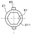
- a recess 81 is formed in the end surface 211 of the first light guide 21 on the side that comes into contact (close contact) with the second light guide 22.
- the recess 81 serves as positioning means.
- the recess 81 is a regular hexagon when viewed from the side surface with the central axis being C1.
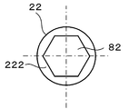
- a convex portion 82 is formed on the end surface 222 of the second light guide 22 on the side that comes into contact (close contact) with the first light guide 21.
- the convex part 82 plays a role as positioning means.
- the convex portion 82 is a regular hexagon as viewed from the side surface with the central axis as C1.
- the convex part 82 is formed in substantially the same size so as to be fitted in the concave part 81 of the first light guide 21.
- the first light guide 21 and the second light guide 22 configured as described above are connected as follows. First, a transparent adhesive (not shown) such as UV curable resin is applied to the end surface 211 of the first light guide 21 or the end surface 222 of the second light guide 22. Next, the concave portion 81 of the first light guide and the convex portion 82 of the second light guide 22 are aligned. And the end surface 211 of the 1st light guide 21 and the end surface 222 of the 2nd light guide 22 are made to adjoin, and the convex part 82 is inserted in the recessed part 81a. Further, the end surface 211 of the first light guide 21 and the end surface 222 of the second light guide 22 are brought close to each other, and as shown in FIG.
- a transparent adhesive such as UV curable resin
- the end surfaces are brought into contact with each other so that the outer peripheries of the end surfaces are aligned. ) Thereby, the end surface 211 of the 1st light guide 21 and the end surface 222 of the 2nd light guide 22 are joined by an adhesive agent.
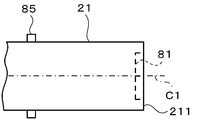
- a convex member 85 is disposed on the side surface of the first light guide 21.
- the lighting device 15 is provided with a spacer 86 so as to cover the convex member 85.
- the spacer 86 is an engaging means for attaching the lighting device 15 to the frame 11.
- the illumination device 15 is attached to the frame 11 by engaging a spacer 86 with an illumination device attachment portion 11 ⁇ / b> A formed on the frame 11.
- the light guide unit of the third embodiment there is no need to provide a fitting member on the side surface of the light guide, unlike the light guide unit of the first embodiment. Compared to the light guide unit of the first embodiment, the number of parts can be reduced.
- Embodiment 4 FIG. Next, a fourth embodiment of the present invention will be described.
- the basic configuration of the contact image sensor 10 is the same as that of the first embodiment.
- the fourth embodiment is different from the first embodiment in that the number of light guides constituting the light guide unit is two.
- the illumination device 100 includes a light guide unit 101, a light emitting diode unit 25, and a holder 29.
- the light guide unit 101 includes two light guides formed in the same manner as the light guide of the first embodiment. Specifically, the light guide unit 101 includes a first light guide 110 and a second light guide 120. The first light guide 110 and the second light guide 120 are arranged in series so that the respective central axes C1 coincide with each other and the side surfaces thereof are flush with each other. The first light guide 110 and the second light guide 120 are adjacent to each other, and their end faces are in contact (contact).
- the first light guide 110 has a pair of sides on the side surface in the vicinity of the end surface on the side in contact (contact) with the second light guide 120.
- First fitting members 28A and 28A are provided.
- the second light guide 120 has a pair of second fitting members 28 ⁇ / b> B on the side surface in the vicinity of the end surface on the first light guide 110 side. , 28B.
- the first light guide 110 and the second light guide 120 are joined in the same procedure as described in the first embodiment.
- the number of light guides is not limited to three as in the first embodiment, and may be two. Good.
- Embodiment 5 FIG. Next, a fifth embodiment of the present invention will be described.
- the basic configuration of the contact image sensor 10 is the same as that of the first embodiment.
- the fifth embodiment is different from the first embodiment in that the number of light guides constituting the light guide unit is n (n is an integer of 3 or more).
- the illumination device 150 includes a light guide unit 200, a light emitting diode unit 25, and a holder 29.
- the light guide unit 200 includes n light guides (n is an integer of 3 or more) formed in the same manner as the light guide of the first embodiment.
- the light guide unit 200 is disposed between the first light guide 210, the third light guide 230, and the first light guide 210 and the third light guide 230 (n). -2)
- the second light guides 220 are arranged in series.
- the first light guide 210, the third light guide 230, and the second light guide 220 are aligned such that the respective central axes C1 coincide with each other and the side surfaces thereof are flush with each other. .
- the end surfaces of the adjacent light guides are in contact (in close contact).
- the first light guide 210 has a pair of first light guides on the side surface in the vicinity of the end surface on the side in contact (contact) with the second light guide 220. 1 fitting members 28A, 28A.
- the second light guide 220 has a pair of second fitting members 28B on the side surface in the vicinity of the end face on the first light guide 210 side. 28B.
- the second light guide 220 includes a pair of first fitting members 28A and 28A on the side surface near the end face on the third light guide 230 side.
- the third light guide body 230 has a pair of first light guides on the side surface in the vicinity of the end face on the side in contact (contact) with the second light guide body 220.
- Two fitting members 28B and 28B are provided.
- the first light guide 210, the second light guide 220, and the third light guide 230 are joined in the same procedure as described in the first embodiment.
- the number of light guides is not limited to three as in the first embodiment, but is more than that. May be.
- the light guide is cylindrical, but the shape of the end face and the cross section of the light guide is not particularly limited, and may be a polygonal column such as a square column. Moreover, as shown in FIG. 15, the shape which cut
- the second light guides 22 and 220 of the above-described embodiment have two types of fitting members, that is, the first fitting member 28A near one end and the second fitting near the other end.
- a first fitting member 28A is arranged on one of the adjacent light guides, and a second fitting member 28B is arranged on the other side so that these fitting members can be fitted to each other.
- the second light guides 22 and 220 may include the same fitting member in the vicinity of both ends.
- This invention is suitable for an optical device such as an image scanner.
Landscapes
- Engineering & Computer Science (AREA)
- Multimedia (AREA)
- Signal Processing (AREA)
- Physics & Mathematics (AREA)
- Optics & Photonics (AREA)
- General Physics & Mathematics (AREA)
- Facsimile Heads (AREA)
- Facsimile Scanning Arrangements (AREA)
- Arrangement Of Elements, Cooling, Sealing, Or The Like Of Lighting Devices (AREA)
- Planar Illumination Modules (AREA)
Priority Applications (4)
| Application Number | Priority Date | Filing Date | Title |
|---|---|---|---|
| EP13751379.2A EP2819389A1 (en) | 2012-02-22 | 2013-02-19 | Light-guide unit and image sensor |
| US14/370,135 US20140374864A1 (en) | 2012-02-22 | 2013-02-19 | Light-guide unit and image sensor |
| KR1020147021761A KR20140111327A (ko) | 2012-02-22 | 2013-02-19 | 도광체 유닛 및 이미지 센서 |
| CN201380010001.8A CN104115477A (zh) | 2012-02-22 | 2013-02-19 | 导光体单元及图像传感器 |
Applications Claiming Priority (2)
| Application Number | Priority Date | Filing Date | Title |
|---|---|---|---|
| JP2012-035955 | 2012-02-22 | ||
| JP2012035955A JP5955021B2 (ja) | 2012-02-22 | 2012-02-22 | 導光体ユニット及びイメージセンサ |
Publications (1)
| Publication Number | Publication Date |
|---|---|
| WO2013125501A1 true WO2013125501A1 (ja) | 2013-08-29 |
Family
ID=49005686
Family Applications (1)
| Application Number | Title | Priority Date | Filing Date |
|---|---|---|---|
| PCT/JP2013/053924 Ceased WO2013125501A1 (ja) | 2012-02-22 | 2013-02-19 | 導光体ユニット及びイメージセンサ |
Country Status (6)
| Country | Link |
|---|---|
| US (1) | US20140374864A1 (https=) |
| EP (1) | EP2819389A1 (https=) |
| JP (1) | JP5955021B2 (https=) |
| KR (1) | KR20140111327A (https=) |
| CN (1) | CN104115477A (https=) |
| WO (1) | WO2013125501A1 (https=) |
Families Citing this family (3)
| Publication number | Priority date | Publication date | Assignee | Title |
|---|---|---|---|---|
| CN103149627B (zh) * | 2013-04-02 | 2016-05-25 | 深圳安嵘光电产品有限公司 | 一种带孔的导光板及其制作方法 |
| US10527780B2 (en) * | 2017-09-07 | 2020-01-07 | Canon Components, Inc. | Illumination apparatus, reading apparatus, and printing apparatus |
| DE102017219094A1 (de) * | 2017-10-25 | 2019-04-25 | Volkswagen Aktiengesellschaft | Leuchtvorrichtung für ein Kraftfahrzeug |
Citations (3)
| Publication number | Priority date | Publication date | Assignee | Title |
|---|---|---|---|---|
| JP2010147859A (ja) * | 2008-12-19 | 2010-07-01 | Panasonic Corp | 線状照明装置及びそれを用いた密着型イメージセンサ及び画像読取システム |
| JP2010212869A (ja) * | 2009-03-09 | 2010-09-24 | Mitsubishi Electric Corp | 密着イメージセンサ |
| JP2010238492A (ja) * | 2009-03-31 | 2010-10-21 | Panasonic Corp | 照明装置 |
Family Cites Families (9)
| Publication number | Priority date | Publication date | Assignee | Title |
|---|---|---|---|---|
| US5969343A (en) * | 1995-08-24 | 1999-10-19 | Matsushita Electric Industrial Co., Ltd. | Linear illumination device |
| JP2001136343A (ja) * | 1999-11-09 | 2001-05-18 | Citizen Electronics Co Ltd | 密着形イメージセンサ |
| US6476986B2 (en) * | 1999-12-28 | 2002-11-05 | Texas Instruments Incorporated | Six-axis attachment apparatus and method for spatial light modulators |
| US7216990B2 (en) * | 2003-12-18 | 2007-05-15 | Texas Instruments Incorporated | Integrated lamp and aperture alignment method and system |
| US7344290B2 (en) * | 2005-09-20 | 2008-03-18 | Ledtech Electronics Corp. | Lamp module |
| CN101374188B (zh) * | 2007-08-22 | 2011-04-20 | 威海华菱光电有限公司 | 图像传感器 |
| JP2009117186A (ja) * | 2007-11-07 | 2009-05-28 | Rohm Co Ltd | 導光体、およびこれを用いたイメージセンサモジュール |
| JP2009303080A (ja) * | 2008-06-16 | 2009-12-24 | Nippon Sheet Glass Co Ltd | 棒状導光体および画像読取装置 |
| JP2012015987A (ja) * | 2010-06-02 | 2012-01-19 | Rohm Co Ltd | 線状光源装置および画像読取装置 |
-
2012
- 2012-02-22 JP JP2012035955A patent/JP5955021B2/ja active Active
-
2013
- 2013-02-19 US US14/370,135 patent/US20140374864A1/en not_active Abandoned
- 2013-02-19 WO PCT/JP2013/053924 patent/WO2013125501A1/ja not_active Ceased
- 2013-02-19 EP EP13751379.2A patent/EP2819389A1/en not_active Withdrawn
- 2013-02-19 CN CN201380010001.8A patent/CN104115477A/zh active Pending
- 2013-02-19 KR KR1020147021761A patent/KR20140111327A/ko not_active Abandoned
Patent Citations (3)
| Publication number | Priority date | Publication date | Assignee | Title |
|---|---|---|---|---|
| JP2010147859A (ja) * | 2008-12-19 | 2010-07-01 | Panasonic Corp | 線状照明装置及びそれを用いた密着型イメージセンサ及び画像読取システム |
| JP2010212869A (ja) * | 2009-03-09 | 2010-09-24 | Mitsubishi Electric Corp | 密着イメージセンサ |
| JP2010238492A (ja) * | 2009-03-31 | 2010-10-21 | Panasonic Corp | 照明装置 |
Also Published As
| Publication number | Publication date |
|---|---|
| JP2013172366A (ja) | 2013-09-02 |
| CN104115477A (zh) | 2014-10-22 |
| JP5955021B2 (ja) | 2016-07-20 |
| KR20140111327A (ko) | 2014-09-18 |
| US20140374864A1 (en) | 2014-12-25 |
| EP2819389A1 (en) | 2014-12-31 |
Similar Documents
| Publication | Publication Date | Title |
|---|---|---|
| US9083832B2 (en) | Image reading device and method of manufacturing housing | |
| US9088684B2 (en) | Image reading device | |
| CA2714696A1 (en) | Optical path change member and holding member body | |
| TWI578051B (zh) | 光連接器 | |
| TW200702591A (en) | Planar lighting apparatus | |
| JP2007225600A5 (https=) | ||
| WO2013125501A1 (ja) | 導光体ユニット及びイメージセンサ | |
| US9557474B2 (en) | Light guide and image reading apparatus | |
| US8493637B2 (en) | Image forming optical element, image forming optical array, and image reading device | |
| WO2019092824A1 (ja) | 導光体、導光体ユニット及びその製造方法、電子機器 | |
| US10674030B2 (en) | Illumination device and image reading device | |
| JP4577657B2 (ja) | 照明装置 | |
| JP5005399B2 (ja) | 照明装置 | |
| JPH10271278A (ja) | 画像読み取り装置 | |
| JP6649090B2 (ja) | 光レセプタクルおよび光モジュール | |
| JP2005195804A (ja) | 光接続構造 | |
| JP2012019333A (ja) | 画像読取装置 | |
| JP2012163742A (ja) | 結像光学素子、結像光学アレイおよび画像読取装置 | |
| JPWO2016194493A1 (ja) | イメージセンサユニット、紙葉類識別装置、画像読取装置 | |
| JP2007298886A (ja) | レンズ部品及び光モジュール | |
| JP2009037190A (ja) | 電子機器の表示装置 | |
| JP2010114045A (ja) | 線状照明装置 | |
| JP2018160781A (ja) | 発光装置、画像読取装置及び画像形成装置 | |
| JP2012151640A (ja) | 画像読取装置 | |
| JP2009204945A (ja) | 光学レンズ及び光ファイバユニット並びに光センサ装置 |
Legal Events
| Date | Code | Title | Description |
|---|---|---|---|
| 121 | Ep: the epo has been informed by wipo that ep was designated in this application |
Ref document number: 13751379 Country of ref document: EP Kind code of ref document: A1 |
|
| WWE | Wipo information: entry into national phase |
Ref document number: 14370135 Country of ref document: US |
|
| ENP | Entry into the national phase |
Ref document number: 20147021761 Country of ref document: KR Kind code of ref document: A |
|
| WWE | Wipo information: entry into national phase |
Ref document number: 2013751379 Country of ref document: EP |
|
| NENP | Non-entry into the national phase |
Ref country code: DE |