WO2013099728A1 - 情報記録媒体用ガラス基板の製造方法 - Google Patents
情報記録媒体用ガラス基板の製造方法 Download PDFInfo
- Publication number
- WO2013099728A1 WO2013099728A1 PCT/JP2012/082895 JP2012082895W WO2013099728A1 WO 2013099728 A1 WO2013099728 A1 WO 2013099728A1 JP 2012082895 W JP2012082895 W JP 2012082895W WO 2013099728 A1 WO2013099728 A1 WO 2013099728A1
- Authority
- WO
- WIPO (PCT)
- Prior art keywords
- glass substrate
- cleaning
- tank
- information recording
- recording medium
- Prior art date
Links
Images


Classifications
-
- G—PHYSICS
- G11—INFORMATION STORAGE
- G11B—INFORMATION STORAGE BASED ON RELATIVE MOVEMENT BETWEEN RECORD CARRIER AND TRANSDUCER
- G11B5/00—Recording by magnetisation or demagnetisation of a record carrier; Reproducing by magnetic means; Record carriers therefor
- G11B5/84—Processes or apparatus specially adapted for manufacturing record carriers
- G11B5/8404—Processes or apparatus specially adapted for manufacturing record carriers manufacturing base layers
Definitions
- the present invention relates to a method for producing a glass substrate for an information recording medium.
- an aluminum substrate or a glass substrate is used as an information recording medium (magnetic disk recording medium) used in a computer or the like.
- a magnetic thin film layer is formed on these substrates, and information is recorded on the magnetic thin film layer by magnetizing the magnetic thin film layer with a magnetic head.
- hard disk drives have been developed that have a recording capacity of 500 GB (single-sided 250 GB), a surface recording density of 630 Gb / square inch or more, with one 2.5-inch recording medium. The distance (flying height) between the head and the information recording medium is further reduced.
- the size of defects on the substrate surface permitted as the information recording medium is also reduced in order to suppress defects (head crashes) when the information recording medium is used in a hard disk drive.
- the demands on the size and the number are increasing.
- a device has been devised to reduce defects in the information recording medium glass substrate by devising polishing and cleaning methods for the information recording medium glass substrate.
- DFH Dynamic Flying Height
- the problem to be solved by the present invention is that the demand for reducing defects in the glass substrate for information recording medium in the manufacturing process of the glass substrate for information recording medium is becoming stricter.
- the present invention has been made in view of the above circumstances, and provides a method for manufacturing a glass substrate for an information recording medium capable of reducing defects that occur during the manufacturing process of the glass substrate for an information recording medium. Objective.
- the method for manufacturing a glass substrate for an information recording medium includes a step of polishing a glass substrate and a step of cleaning the glass substrate after polishing the glass substrate.
- the step of cleaning the glass substrate is performed after the step of cleaning the glass substrate in the first tank whose inner surface is made of stainless steel or resin and the step of cleaning the glass substrate in the first tank are completed. And a step of cleaning the glass substrate in the second tank whose inner surface is made of quartz.
- the value of the zeta potential of impurities attached to the glass substrate, the value of the zeta potential of the stainless steel and the resin, and the value of the zeta potential of the glass substrate are all the same sign, and from the absolute value of the zeta potential of the stainless steel and the resin However, the absolute value of the zeta potential of the glass substrate is larger.
- the “impurities attached to the glass substrate” is a concept including one or both of those derived from the polishing step attached in the glass substrate polishing step and those derived from the material of the cleaning tank. .
- the difference between the absolute value of the zeta potential of impurities and the absolute value of the zeta potential of stainless steel and resin is 10 mV or more in the method for manufacturing a glass substrate for an information recording medium.
- the inner surface of the first tank is made of one material selected from the group consisting of polyvinyl chloride, polytetrafluoroethylene, polypropylene, and polycarbonate. .
- the step of cleaning the glass substrate is performed on the glass substrate before performing the step of cleaning the glass substrate in the second tank. Including a step of scrub cleaning.
- the step of cleaning the glass substrate in the second tank includes applying an ultrasonic wave having a frequency of 900 kHz or more to the glass substrate.
- the present invention it is possible to reduce defects that occur in the manufacturing process of the glass substrate for information recording media.
- FIG. 1 is a perspective view of an information recording medium glass substrate 1G
- FIG. 2 is a perspective view of the information recording medium.
- an information recording medium glass substrate 1G used for the information recording medium 1 (hereinafter referred to as “glass substrate 1G”) has an annular disk shape with a hole 11 formed in the center. ing.
- the glass substrate 1G has an outer peripheral end face 12, an inner peripheral end face 13, a front main surface 14, and a back main surface 15.
- amorphous glass or the like is used as the glass substrate 1G.
- the outer diameter is about 65 mm
- the inner diameter is about 20 mm
- the thickness is about 0.8 mm
- the surface roughness is about 2.0 mm or less.
- the inch size of the glass substrate 1G is not particularly limited, and various glass substrates 1G of 0.8 inch, 1.0 inch, 1.8 inch, 2.5 inch, and 3.5 inch are manufactured as disks for information recording media. May be.
- the thickness of the glass substrate 1G is preferably 0.30 mm to 2.2 mm because it is effective against cracking of the glass substrate 1G due to drop impact.
- the thickness of the glass substrate 1 ⁇ / b> G here means an average value of values measured at some arbitrary points to be pointed on the substrate.
- a magnetic thin film layer 23 is formed on the front main surface 14 of the glass substrate 1G.
- the magnetic thin film layer 23 is formed only on the front main surface 14, but it is also possible to provide the magnetic thin film layer 23 on the back main surface 15.
- a conventionally known method can be used as a method for forming the magnetic thin film layer 23 .
- a method of spin-coating a thermosetting resin in which magnetic particles are dispersed a method of forming by sputtering, a method of electroless The method of forming by plating is mentioned.
- the film thickness by spin coating is about 0.3 to 1.2 ⁇ m
- the film thickness by sputtering is about 0.04 to 0.08 ⁇ m
- the film thickness by electroless plating is 0.05 to 0.1 ⁇ m. From the viewpoint of thinning and high density, film formation by sputtering and electroless plating is preferable.
- the magnetic material used for the magnetic thin film layer 23 is not particularly limited, and a conventionally known material can be used. However, in order to obtain a high coercive force, Co having a high crystal anisotropy is basically used to adjust the residual magnetic flux density. Co-based alloys to which Ni and Cr are added are suitable. In recent years, FePt-based materials have been used as magnetic layer materials suitable for heat-assisted recording.
- the surface of the magnetic thin film layer 23 may be thinly coated with a lubricant.
- a lubricant include those obtained by diluting perfluoropolyether (PFPE), which is a liquid lubricant, with a freon-based solvent.
- the underlayer in the information recording medium 1 is selected according to the magnetic film.
- the material for the underlayer include at least one material selected from nonmagnetic metals such as Cr, Mo, Ta, Ti, W, V, B, Al, and Ni.
- the underlayer is not limited to a single layer, and may have a multi-layer structure in which the same or different layers are stacked.
- a multilayer underlayer such as Cr / Cr, Cr / CrMo, Cr / CrV, NiAl / Cr, NiAl / CrMo, or NiAl / CrV may be used.
- Examples of the protective layer for preventing wear and corrosion of the magnetic thin film layer 23 include a Cr layer, a Cr alloy layer, a carbon layer, a hydrogenated carbon layer, a zirconia layer, and a silica layer.
- the protective layer can be formed continuously with an in-line sputtering apparatus, such as an underlayer and a magnetic film.
- the protective layer may be a single layer, or may have a multilayer structure composed of the same or different layers.
- Another protective layer may be formed on the protective layer or instead of the protective layer.
- tetraalkoxylane is diluted with an alcohol-based solvent on a Cr layer, and then colloidal silica fine particles are dispersed and applied, followed by baking to form a silicon oxide (SiO 2 ) layer. It may be formed.
- FIG. 3 is a flowchart showing a method for manufacturing the glass substrate 1G and the information recording medium 1.
- step 10 a “glass melting step” of step 10 (hereinafter abbreviated as “S10”, the same applies to step 11 and subsequent steps), the glass material constituting the glass substrate is melted.
- a glass substrate was produced by pressing the molten glass material using an upper mold and a lower mold.
- the glass composition used was a general aluminosilicate glass.
- the method for producing the glass substrate is not limited to molding, and may be cut out from plate glass, which is a known technique, and the glass composition is not limited thereto.
- both main surfaces of the glass substrate were lapped.
- This first lapping step was performed using a double-sided lapping device using a planetary gear mechanism. Specifically, the lapping platen was pressed on both surfaces of the glass substrate from above and below, the grinding liquid was supplied onto the main surface of the glass substrate, and these were moved relatively to perform lapping. By this lapping process, a glass substrate having a substantially flat main surface was obtained.
- a hole was formed in the center of the glass substrate using a cylindrical diamond drill to produce an annular glass substrate.
- the inner peripheral end surface and the outer peripheral end surface of the glass substrate were ground with a diamond grindstone, and a predetermined chamfering process was performed.
- the fine uneven shape formed on the main surface in the coring and end face processing in the previous step can be removed in advance. As a result, the polishing time of the main surface in the subsequent process can be shortened.
- the outer peripheral end surface of the glass substrate was subjected to mirror polishing by brush polishing.
- a slurry containing general cerium oxide abrasive grains was used as the abrasive grains.
- the main surface was polished.
- the first polishing step is mainly intended to correct scratches and warpage remaining on the main surface in the first and second lapping steps (S12, S14) described above.
- the main surface was polished by a double-side polishing apparatus having a planetary gear mechanism.
- the abrasive general cerium oxide abrasive grains were used.
- a surface reinforcing layer was formed on the main surface of the glass substrate 1G.
- chemical strengthening was performed by immersing the glass substrate 1G in a mixed solution of potassium nitrate (70%) and sodium nitrate (30%) heated to 300 ° C. for about 30 minutes.
- the lithium ion and sodium ion on the inner peripheral end surface and outer peripheral end surface of the glass substrate are respectively replaced with sodium ions and potassium ions in the chemical strengthening solution, and a compressive stress layer is formed, thereby forming the main surface of the glass substrate and The end face was strengthened.
- the main surface polishing step was performed in the “second polishing step” of S18.
- This second polishing step aims to eliminate the fine defects on the main surface that have been generated and remain in the above-described steps and finish it in a mirror shape, to eliminate warpage and finish it to a desired flatness.
- polishing was performed by a double-side polishing apparatus having a planetary gear mechanism.
- abrasive colloidal silica having an average particle diameter of about 20 nm was used to obtain a smooth surface.
- an adhesion layer made of a Cr alloy, a soft magnetic layer made of a CoFeZr alloy, Ru An information recording medium of a perpendicular magnetic recording system was manufactured by sequentially forming an orientation control underlayer made of, a perpendicular magnetic recording layer made of a CoCrPt alloy, a C-based protective layer, and an F-based lubricating layer.
- This configuration is an example of a configuration of a perpendicular magnetic recording system, and a magnetic layer or the like may be configured as an in-plane information recording medium.
- the “post-heat treatment step” of S21 is performed to complete the information recording medium.
- the final cleaning step (S19) includes a step of cleaning the glass substrate in a first tank whose inner surface (surface in contact with the cleaning liquid) is made of stainless steel or resin, and a second tank whose inner surface is made of quartz. And a step of cleaning the glass substrate.
- a plurality of first tanks and second tanks may be provided, or one tank may be provided.
- the cleaning tank whose inner surface is made of stainless steel, resin, and quartz may be referred to as a stainless steel tank, a resin tank, and a quartz tank, respectively.
- the first tank is a tank made entirely of stainless steel, or is a tank made by coating resin on the inner surface of a tank made entirely of stainless steel
- the second tank is a tank made entirely of quartz.
- a tank made entirely of resin may be used as the resin layer, or a double-layer structure in which a propagation liquid is placed in an outer tank made of stainless steel and an inner tank made of quartz is provided in the propagation liquid (outside An ultrasonic generator is attached to the outer surface of the tank, and a cleaning solution is put into the inner tank).
- the step of cleaning the glass substrate in each of the first tank and the second tank may include ultrasonic cleaning.
- the step of cleaning the glass substrate in the second tank is performed after the step of cleaning the glass substrate in the first tank is completed.
- a step of scrub cleaning the glass substrate may be provided before the step of cleaning the glass substrate in the second tank.
- the resin constituting the first tank examples include polyvinyl chloride (PVC), polytetrafluoroethylene (PTFE), polypropylene (PP), and polycarbonate (PC). Further, typically, the thickness of the first tank is, for example, about 0.03 ⁇ m or more and 0.6 ⁇ m or less, and the thickness of the second tank is typically larger than the thickness of the first tank, for example, 1 cm or more. It is about 3 cm or less.
- PVC polyvinyl chloride
- PTFE polytetrafluoroethylene
- PP polypropylene
- PC polycarbonate
- the idea of performing the final cleaning in the quartz tank after the cleaning in the stainless steel tank or the resin tank is adopted. That is, in this embodiment, the deposits derived from the polishing step are removed by washing in the first tank (stainless steel tank or resin tank), and the deposits derived from the washing tank are removed in the second tank (quartz tank). The idea of removing by washing is adopted.
- ultrasonic cleaning is performed at a relatively large frequency (for example, 900 kHz or more).
- a relatively large frequency for example, 900 kHz or more.
- the impurities attached to the glass substrate, the inner surface of the first tank, and the zeta potential of the glass substrate Adjust the magnitude relationship. Specifically, the zeta potential value ( ⁇ 1) of impurities (typically colloidal silica derived from the polishing process) adhering to the glass substrate, the zeta potential value ( ⁇ 2) of the inner surface of the first tank, The zeta potential value ( ⁇ 3) of the glass substrate is all the same sign (typically, both are negative), and the glass plate is smaller than the absolute value (
- the above zeta potentials can be controlled by adjusting the material on the inner surface of the cleaning tank and the pH of the cleaning liquid.
- ) of the inner surface of the first tank is about 10 mV or more. Adjusted.
- the value of the zeta potential varies depending on the material of the glass substrate and the material of the cleaning tank. For example, if the cleaning tank is made of resin and the pH of the cleaning liquid is increased (to the strong alkali side), the absolute value of the zeta potential of the deposit on the glass substrate and the absolute value of the zeta potential of the inner surface of the cleaning tank There is a tendency for the difference between the two to increase.
- the cleaning tank has an adjusting means for adjusting the zeta potential.
- sodium hydroxide (NaOH) or potassium hydroxide (KOH) is added, and when reducing the pH of the cleaning solution (to the acid side), Adjust by adding hydrochloric acid (HCl) or sulfuric acid (H 2 SO 4 ).
- the difference between the zeta potential and the zeta potential is adjusted to be about 10 mV or more as described above.
- the cleaning process is performed using two types of cleaning tanks separately, and the zeta potential magnitude relationship is set so that impurities can be more effectively removed in the cleaning process in the first tank.
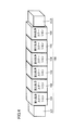
- the first cleaning station 101, the second cleaning station 102, and the fourth cleaning station 104 use a resin tank in which the inner surface of the stainless steel tank is coated with PVC (polyvinyl chloride), and the third cleaning station.
- PVC polyvinyl chloride
- a resin tank in which the inner surface of the stainless steel tank was coated with PTFE (polytetrafluoroethylene) was used, and in the fifth cleaning station 105, a quartz tank made of quartz was used for the entire tank.
- FIG. 5 shows the relationship between the zeta potential of the glass substrate, resin tank, quartz tank and colloidal silica (deposits derived from the polishing process) having the above composition and the hydrogen ion index (pH) of the cleaning liquid.
- the resin tank A in FIG. 5 is a resin tank in which the inner surface of the stainless steel tank is coated with PVC
- the resin tank B is a resin tank in which the inner surface of the stainless steel tank is coated with PTFE.
- each zeta potential varies depending on the hydrogen ion index of the cleaning liquid
- the above-described zeta potential magnitude relationship can be obtained by adjusting the hydrogen ion index of the cleaning liquid and the material on the inner surface of the resin tank. Is possible.
- the average number of defects is smaller in Examples 1 to 3 than in Comparative Examples 1 to 4. That is, in Examples 1 to 3, the number of defects in the glass substrate can be reduced as compared with Comparative Examples 1 to 4.
- the third cleaning station 103 was not coated with a resin, and the same evaluation was performed by adjusting the zeta potential of the wall surface of the stainless steel tank by applying a charge to the stainless steel tank as a stainless steel tank. Results were obtained.
- the electromagnetic conversion characteristic inspection is similar to recording / reproduction of a normal hard disk drive, in which a predetermined signal is recorded on a magnetic recording medium with a magnetic head, and then the signal is reproduced. By detecting the recording failure of the recording medium, the quality of the magnetic recording medium, such as the electrical characteristics of the magnetic recording medium and the presence or absence of defects, is confirmed.
- the present invention is applicable to a method for manufacturing a glass substrate for an information recording medium.
- 1 information recording medium 1G glass substrate for information recording medium, 11 holes, 12 outer peripheral end face, 13 inner peripheral end face, 14 front main surface, 15 back main surface, 23 magnetic thin film layer.
Abstract
ガラス基板の製造方法は、ガラス基板の研磨を行なう工程と、ガラス基板の研磨を行なった後に、ガラス基板の洗浄を行なう工程とを備える。ガラス基板の洗浄を行なう工程は、槽内面がステンレスまたは樹脂からなる第1槽の中でガラス基板の洗浄を行なう工程と、第1槽の中でガラス基板の洗浄を行なう工程が完了した後に行なわれ、槽内面が石英からなる第2槽の中でガラス基板の洗浄を行なう工程とを含む。ガラス基板に付着した不純物のゼータ電位の値と、上記ステンレスおよび上記樹脂のゼータ電位の値と、ガラス基板のゼータ電位の値とが全て同符号であり、ステンレスおよび樹脂のゼータ電位の絶対値よりも、ガラス基板のゼータ電位の絶対値の方が大きい。
Description
本発明は、情報記録媒体用ガラス基板の製造方法に関する。
コンピュータなどに用いられる情報記録媒体(磁気ディスク記録媒体)には、従来からアルミニウム基板またはガラス基板が用いられている。これらの基板上に磁気薄膜層が形成され、磁気薄膜層を磁気ヘッドで磁化することにより、磁気薄膜層に情報が記録される。
近年、ハードディスクドライブ装置においては、2.5インチの記録媒体1枚で、記録容量が500GB(片面250GB)、面記録密度が630Gb/平方インチ以上の記録密度を有するものが開発されており、磁気ヘッドと情報記録媒体との間の距離(フライングハイト)がさらに小さくなってきている。
フライングハイトが小さくなるにつれて、情報記録媒体をハードディスクドライブ装置に用いた場合の不良(ヘッドクラッシュ)を抑えるために、情報記録媒体として許容される基板表面の欠陥の大きさもより小さくなってきている。また、情報記録媒体用ガラス基板の表面欠陥についても大きさおよび個数に対する要求が厳しくなってきている。
これらの厳しい要求を満足するために、情報記録媒体用ガラス基板の研磨加工、洗浄方法を工夫して情報記録媒体用ガラス基板の欠陥を低減すべく工夫がなされている。しかし、磁気ヘッドに採用されるDFH(Dynamic Flying Height)機構等により、ますます情報記録媒体への精度が厳しくなってきている。
この発明が解決しようとする課題は、情報記録媒体用ガラス基板の製造過程における、情報記録媒体用ガラス基板の欠陥低減の要求が厳しくなってきている点にある。
情報記録媒体用ガラス基板の欠陥を低減するために、該基板の高い清浄性および高い平滑性が求められる。
たとえば、半導体ウエハを洗浄する場合には、石英槽に被洗浄物を浸し、超音波を印加することが行なわれている(たとえば、特許文献1)。
しかし、複数の洗浄槽を用いてガラス基板の洗浄を行なうにあたり、単純に洗浄槽をすべて石英槽にすれば、ガラス基板に付着した付着物を十分に落とすことができるというものではない。
本発明は、上記の実情に鑑みてなされたものであって、情報記録媒体用ガラス基板の製造過程で生じる不良を低減することが可能な情報記録媒体用ガラス基板の製造方法を提供することを目的とする。
本発明に係る情報記録媒体用ガラス基板の製造方法は、ガラス基板の研磨を行なう工程と、ガラス基板の研磨を行なった後に、ガラス基板の洗浄を行なう工程とを備える。
ガラス基板の洗浄を行なう工程は、槽内面がステンレスまたは樹脂からなる第1槽の中でガラス基板の洗浄を行なう工程と、第1槽の中でガラス基板の洗浄を行なう工程が完了した後に行なわれ、槽内面が石英からなる第2槽の中でガラス基板の洗浄を行なう工程とを含む。
ガラス基板に付着した不純物のゼータ電位の値と、上記ステンレスおよび上記樹脂のゼータ電位の値と、ガラス基板のゼータ電位の値とが全て同符号であり、ステンレスおよび樹脂のゼータ電位の絶対値よりも、ガラス基板のゼータ電位の絶対値の方が大きい。
なお、本明細書において、「ガラス基板に付着した不純物」とは、ガラス基板の研磨工程において付着した研磨工程由来のものと、洗浄槽の材質由来のものとの一方または両方を含む概念である。
1つの実施態様では、上記情報記録媒体用ガラス基板の製造方法において、不純物のゼータ電位の絶対値と、ステンレスおよび樹脂のゼータ電位の絶対値との差が10mV以上である。
1つの実施態様では、上記情報記録媒体用ガラス基板の製造方法において、第1槽の槽内面は、ポリ塩化ビニル、ポリテトラフルオロエチレン、ポリプロピレンおよびポリカーボネートからなる群のうちの1つの素材からなる。
1つの実施態様では、上記情報記録媒体用ガラス基板の製造方法において、ガラス基板の洗浄を行なう工程は、第2槽の中でガラス基板の洗浄を行なう工程を行なう前に、ガラス基板に対してスクラブ洗浄を行なう工程を含む。
1つの実施態様では、上記情報記録媒体用ガラス基板の製造方法において、第2槽の中でガラス基板の洗浄を行なう工程は、900kHz以上の周波数の超音波をガラス基板に印加することを含む。
本発明によれば、情報記録媒体用ガラス基板の製造過程で生じる不良を低減することができる。
以下に、本発明の実施の形態および実施例について説明する。なお、同一または相当する部分に同一の参照符号を付し、その説明を繰返さない場合がある。
なお、以下に説明する実施の形態および実施例において、個数、量などに言及する場合、特に記載がある場合を除き、本発明の範囲は必ずしもその個数、量などに限定されない。また、以下の実施の形態において、各々の構成要素は、特に記載がある場合を除き、本発明にとって必ずしも必須のものではない。
(情報記録媒体1の構成)
図1および図2を参照して、情報記録媒体用ガラス基板1Gおよび情報記録媒体1の構成について説明する。図1は、情報記録媒体用ガラス基板1Gの斜視図、図2は、情報記録媒体の斜視図である。
図1および図2を参照して、情報記録媒体用ガラス基板1Gおよび情報記録媒体1の構成について説明する。図1は、情報記録媒体用ガラス基板1Gの斜視図、図2は、情報記録媒体の斜視図である。
図1に示すように、情報記録媒体1に用いられる情報記録媒体用ガラス基板1G(以下、「ガラス基板1G」と称する。)は、中心に孔11が形成された環状の円板形状を呈している。ガラス基板1Gは、外周端面12、内周端面13、表主表面14、および裏主表面15を有している。ガラス基板1Gとしては、アモルファスガラス等を用い、たとえば、外径約65mm、内径約20mm、厚さ約0.8mm、表面粗さは、約2.0Å以下である。
ガラス基板1Gのインチサイズに特に限定はなく、0.8インチ、1.0インチ、1.8インチ、2.5インチ、3.5インチ各種ガラス基板1Gを、情報記録媒体用のディスクとして製造してもよい。
落下衝撃によるガラス基板1Gの割れに対して有効であることから、ガラス基板1Gの厚みは0.30mm~2.2mmが好ましい。ここでいうガラス基板1Gの厚みとは基板上の点対象となる任意の何点かで測定した値の平均値を意味する。
図2に示すように、情報記録媒体1は、上記したガラス基板1Gの表主表面14上に磁気薄膜層23が形成されている。図示では、表主表面14上にのみ磁気薄膜層23が形成されているが、裏主表面15上に磁気薄膜層23を設けることも可能である。
磁気薄膜層23の形成方法としては従来公知の方法を用いることができ、例えば磁性粒子を分散させた熱硬化性樹脂を基板上にスピンコートして形成する方法、スパッタリングにより形成する方法、無電解めっきにより形成する方法が挙げられる。
スピンコート法での膜厚は約0.3~1.2μm程度、スパッタリング法での膜厚は0.04~0.08μm程度、無電解めっき法での膜厚は0.05~0.1μm程度であり、薄膜化および高密度化の観点からはスパッタリング法および無電解めっき法による膜形成がよい。
磁気薄膜層23に用いる磁性材料としては、特に限定はなく従来公知のものが使用できるが、高い保持力を得るために結晶異方性の高いCoを基本とし、残留磁束密度を調整する目的でNi、Crを加えたCo系合金などが好適である。近年では、熱アシスト記録用に好適な磁性層材料として、FePt系の材料が用いられるようになってきている。
磁気ヘッドの滑りをよくするために磁気薄膜層23の表面に潤滑剤を薄くコーティングしてもよい。潤滑剤としては、例えば液体潤滑剤であるパーフロロポリエーテル(PFPE)をフレオン系などの溶媒で希釈したものが挙げられる。
必要により下地層、保護層を設けてもよい。情報記録媒体1における下地層は磁性膜に応じて選択される。下地層の材料としては、例えば、Cr、Mo、Ta、Ti、W、V、B、Al、Niなどの非磁性金属から選ばれる少なくとも一種以上の材料が挙げられる。
下地層は単層とは限らず、同一又は異種の層を積層した複数層構造としても構わない。例えば、Cr/Cr、Cr/CrMo、Cr/CrV、NiAl/Cr、NiAl/CrMo、NiAl/CrV等の多層下地層としてもよい。
磁気薄膜層23の摩耗、腐食を防止する保護層としては、例えば、Cr層、Cr合金層、カーボン層、水素化カーボン層、ジルコニア層、シリカ層などが挙げられる。保護層は、下地層、磁性膜など共にインライン型スパッタ装置で連続して形成できる。保護層は、単層としてもよく、あるいは、同一又は異種の層からなる多層構成としてもよい。
上記保護層上に、あるいは上記保護層に替えて、他の保護層を形成してもよい。例えば、上記保護層に替えて、Cr層の上にテトラアルコキシランをアルコール系の溶媒で希釈した中に、コロイダルシリカ微粒子を分散して塗布し、さらに焼成して酸化ケイ素(SiO2)層を形成してもよい。
(ガラス基板1Gの製造工程)
次に、図3を参照して、本実施の形態に係るガラス基板1Gおよび情報記録媒体1の製造方法を説明する。図3は、ガラス基板1Gおよび情報記録媒体1の製造方法を示すフロー図である。
次に、図3を参照して、本実施の形態に係るガラス基板1Gおよび情報記録媒体1の製造方法を説明する。図3は、ガラス基板1Gおよび情報記録媒体1の製造方法を示すフロー図である。
まず、ステップ10(以下、「S10」と略す。ステップ11以降も同様。)の「ガラス溶融工程」において、ガラス基板を構成するガラス素材を溶融する。
S11の「プレス成形工程」において、溶融させたガラス素材を上型および下型を用いたプレスによりガラス基板を作製した。使用したガラス組成は、一般的なアルミノシリケートガラスを用いた。ガラス基板の作製方法としては成形に限らず、公知の手法である板ガラスからの切り出し等でも構わず、ガラス組成もこれに限らない。
S12の「第1ラップ工程」において、ガラス基板の両主表面をラッピング加工した。この第1ラップ工程は、遊星歯車機構を利用した両面ラッピング装置を用いて行なった。具体的には、ガラス基板の両面に上下からラップ定盤を押圧させ、研削液をガラス基板の主表面上に供給し、これらを相対的に移動させてラッピング加工を行なった。このラッピング加工により、おおよそ平坦な主表面を有するガラス基板を得た。
S13の「コアリング工程」において、円筒状のダイヤモンドドリルを用いて、ガラス基板の中心部に穴を形成し、円環状のガラス基板を作製した。ガラス基板の内周端面、および外周端面をダイヤモンド砥石によって研削し、所定の面取り加工を実施した。
S14の「第2ラップ工程」において、ガラス基板の両主表面について、上記第1ラップ工程(S12)と同様に、ラッピング加工を行なった。この第2ラップ工程を行なうことにより、前工程のコアリングや端面加工において主表面に形成された微細な凹凸形状を予め除去しておくことができる。その結果、後工程での主表面の研磨時間を短縮することができる。
S15の「外周研磨工程」において、ガラス基板の外周端面について、ブラシ研磨による鏡面研磨を行なった。このとき研磨砥粒としては、一般的な酸化セリウム砥粒を含むスラリーを用いた。
S16の「第1ポリッシュ工程」において、主表面研磨を行なった。この第1ポリッシュ工程は、上述の第1および第2ラップ工程(S12,S14)において主表面に残留したキズや反りを矯正することを主目的とするものである。この第1ポリッシュ工程においては、遊星歯車機構を有する両面研磨装置により主表面の研磨を行なった。研磨剤としては、一般的な酸化セリウム砥粒を用いた。
S17の「化学強化工程」において、ガラス基板1Gの主表面に対して表面強化層を形成した。具体的には、300℃に加熱された硝酸カリウム(70%)と硝酸ナトリウム(30%)の混合溶液中に、ガラス基板1Gを約30分間浸漬することによって化学強化を行なった。その結果、ガラス基板の内周端面および外周端面のリチウムイオンおよびナトリウムイオンが、化学強化溶液中のナトリウムイオンおよびカリウムイオンにそれぞれ置換され、圧縮応力層が形成されることでガラス基板の主表面及び端面が強化された。
S18の「第2ポリッシュ工程」において、主表面研磨工程を施した。この第2ポリッシュ工程は上述までの工程で発生、残存している主表面上の微小欠陥等を解消して鏡面状に仕上げること、反りを解消し所望の平坦度に仕上げることを目的とする。この第2ポリッシュ工程は、遊星歯車機構を有する両面研磨装置により研磨を行なった。研磨剤としては、平滑面を得る為に平均粒径が約20nmのコロイダルシリカを用いた。
S19の「最終洗浄工程(Final Cleaning)」において、ガラス基板の主表面、端面の最終洗浄を実施する。これによりガラス基板上に残存する付着物を除去する。
S20の「磁気薄膜層成膜工程」において、上述の工程を経て得られたガラス基板の洗浄後に、ガラス基板の両主表面に、Cr合金からなる密着層、CoFeZr合金からなる軟磁性層、Ruからなる配向制御下地層、CoCrPt合金からなる垂直磁気記録層、C系の保護層、F系からなる潤滑層を順次成膜することにより、垂直磁気記録方式の情報記録媒体を製造した。この構成は垂直磁気記録方式の構成の一例であり、面内情報記録媒体として磁性層等を構成してもよい。その後、S21の「後熱処理工程」を実施することで、情報記録媒体が完成する。
(最終洗浄工程(S19)の実施形態)
以下、上述した最終洗浄工程(S19)の具体的な実施形態について説明する。最終洗浄工程(S19)は、槽内面(洗浄液と接する面)がステンレスまたは樹脂からなる第1槽の中でガラス基板の洗浄を行なう工程と、槽内面が石英からなる第2槽の中でガラス基板の洗浄を行なう工程とを含む。第1槽および第2槽は、各々複数設けられていてもよいし、1つであってもよい。
以下、上述した最終洗浄工程(S19)の具体的な実施形態について説明する。最終洗浄工程(S19)は、槽内面(洗浄液と接する面)がステンレスまたは樹脂からなる第1槽の中でガラス基板の洗浄を行なう工程と、槽内面が石英からなる第2槽の中でガラス基板の洗浄を行なう工程とを含む。第1槽および第2槽は、各々複数設けられていてもよいし、1つであってもよい。
本明細書では、槽内面がステンレス、樹脂および石英からなる洗浄槽を、各々、ステンレス槽、樹脂槽および石英槽と称する場合がある。
典型的な例では、第1槽は、全体がステンレスからなる槽であるか、全体がステンレスからなる槽の内面に樹脂をコーティングした槽であり、第2槽は、全体が石英からなる槽であるが、第1槽、第2槽の態様は、上記のものに限定されない。たとえば、全体が樹脂からなる槽を樹脂層として用いてもよいし、ステンレスからなる外槽に伝播液を入れ、その伝播液の中に石英からなる内槽を設けた二重構造のもの(外槽の外面に超音波発生器を取付け、内槽に洗浄液を入れる。)を石英槽として用いてもよい。
第1槽および第2槽の中でガラス基板の洗浄を各々行なう工程は、超音波洗浄を含むものであってもよい。第2槽の中でガラス基板の洗浄を行なう工程は、第1槽の中でガラス基板の洗浄を行なう工程が完了した後に行なわれる。また、第2槽の中でガラス基板の洗浄を行なう工程を行なう前に、ガラス基板に対してスクラブ洗浄を行なう工程が設けられてもよい。
第1槽を構成する樹脂としては、たとえば、ポリ塩化ビニル(PVC)、ポリテトラフルオロエチレン(PTFE)、ポリプロピレン(PP)およびポリカーボネート(PC)などが考えられる。また、典型的には、第1槽の厚みは、たとえば0.03μm以上0.6μm以下程度であり、第2槽の厚みは、典型的には第1槽の厚みよりも大きく、たとえば1cm以上3cm以下程度である。
ところで、槽内面がステンレスまたは樹脂からなる洗浄槽において洗浄を行なった場合、ステンレス成分や樹脂成分がガラス基板に付着し、これが、後の工程においてエラーを引き起こす要因になり得ることが懸念される。特に、ステンレス成分の影響は大きい。
他方、槽内面が石英からなる洗浄槽だけを用いた場合、超音波洗浄を行なっても、研磨工程で付着した付着物を十分に除去することができない。この原因について、本願発明者が鋭意検討した結果、石英槽においては、超音波洗浄の際の振動板となる板厚のばらつきが大きいため、超音波の減衰率にばらつきが生じ、洗浄にもムラが生じやすいためであることが判明した。
また、石英槽に対してアルカリ性の洗浄液を用いた場合、石英が溶け出す可能性がある。
そこで、本実施の形態では、ステンレス槽または樹脂槽において洗浄を行なった後、石英槽において最終の洗浄を行なうという思想を採用している。すなわち、本実施の形態では、研磨工程由来の付着物については、第1槽(ステンレス槽または樹脂槽)における洗浄で除去し、洗浄槽由来の付着物については、第2槽(石英槽)における洗浄で除去するという思想を採用している。
典型的な例では、石英槽では、比較的大きな周波数(一例としては、900kHz以上)の超音波洗浄を行なう。大きな周波数の超音波洗浄を行なうことにより、ステンレス槽または樹脂槽での洗浄工程では除去し切れなかった微小な付着物を除去することが可能である。
さらに、本実施の形態では、第1槽での洗浄において、ガラス基板から付着物をより効果的に除去するために、ガラス基板に付着した不純物、第1槽内面およびガラス基板のゼータ電位の大小関係を調整する。具体的には、ガラス基板に付着した不純物(典型的には、研磨工程由来のコロイダルシリカ等)のゼータ電位の値(ζ1)と、第1槽内面のゼータ電位の値(ζ2)と、ガラス基板のゼータ電位の値(ζ3)とが全て同符号(典型的には、いずれもマイナス)であり、かつ、第1槽内面のゼータ電位の絶対値(|ζ2|)よりも、ガラス基板のゼータ電位の絶対値(|ζ3|)の方が大きくなるようにする。
上記各ゼータ電位は、洗浄槽内面の材質や、洗浄液のpHを調整することで、制御可能である。好ましくは、研磨工程由来の付着物のゼータ電位の絶対値(|ζ1|)と、第1槽内面のゼータ電位の絶対値(|ζ2|)との差は、10mV以上程度となるように調整される。
なお、同じ洗浄液を用いても、ガラス基板の材質や洗浄槽の材質によって、ゼータ電位の値は変動する。たとえば、洗浄槽の材質が樹脂である場合、洗浄液のpHを大きく(強アルカリ側に)すると、ガラス基板への付着物のゼータ電位の絶対値と、洗浄槽内面のゼータ電位の絶対値との差が大きくなる傾向にある。
このように、洗浄槽は、ゼータ電位を調整するための調整手段を有している。なお、洗浄液のpHを大きく(強アルカリ側に)する場合には、水酸化ナトリウム(NaOH)や水酸化カリウム(KOH)を投入し、洗浄液のpHを小さく(酸性側に)する場合には、塩酸(HCl)や硫酸(H2SO4)を投入して調整する。
上記のようにゼータ電位の大小関係を調整することにより、第1槽での洗浄工程において、洗浄槽中に存する不純物は、第1槽内面およびガラス基板の両方に対して反発するが、ガラス基板に対してより強く反発する。この結果、不純物は、第1槽の中に残されやすくなり、ガラス基板には付着しにくくなる。しかし、洗浄槽に強く付着したり洗浄槽上で堆積して不純物が凝集したりすると洗浄液の汚れやガラス基板への再付着の原因となる場合がある為、洗浄槽壁面と不純物(付着物)とのゼータ電位の差も上記のように10mV以上程度となるように調整されることが好ましい。
このように、本実施の形態では、2種類の洗浄槽を使い分けて洗浄工程を実施するとともに、第1槽での洗浄工程において、不純物をより効果的に除去できようにゼータ電位の大小関係を調整することにより、結果として、情報記録媒体用ガラス基板の製造過程における不良の原因となる付着物を効果的に除去することができる。
<実施例>
以下、上述した最終洗浄工程(S19)の具体的な洗浄工程を、実施例および比較例として説明する。
以下、上述した最終洗浄工程(S19)の具体的な洗浄工程を、実施例および比較例として説明する。
上記「最終洗浄工程(S19)」において、図4に示す洗浄装置100を用いて、ガラス基板の洗浄を実施した。この洗浄装置100は、ガラス基板ロードステーションLD、第1洗浄ステーション101(フッ化水素を添加した酸洗浄、pH=3)、第2洗浄ステーション102(純水を用いた洗浄)、第3洗浄ステーション103(酸性洗剤を用いた洗浄、pH=3)、第4洗浄ステーション104(純水を用いた超音波洗浄:130kHz)、第5洗浄ステーション105(純水を用いた超音波洗浄:950kHz)、第6洗浄ステーション106(IPA乾燥)およびガラス基板アンロードステーションULDを有し、各ステーション間をガラス基板が順次搬送される。
尚、実施例1~3および比較例1~4においては、何れも全6槽からなる洗浄槽で洗浄工程を行なった。
本実施例においては、第1洗浄ステーション101、第2洗浄ステーション102、第4洗浄ステーション104では、ステンレス槽の内面にPVC(ポリ塩化ビニル)のコーティングを施した樹脂槽を用い、第3洗浄ステーション103ではステンレス槽の内面にPTFE(ポリテトラフルオロエチレン)のコーティングを施した樹脂槽を用い、第5洗浄ステーション105では、槽全体が石英からなる石英槽を用いた。
また、ガラス基板としては、次の条件のものを用いている。
SiO2 50-70%
Al2O3 0-20%
B2O3 0-5%
但し、SiO2+Al2O3+B2O3=50-85%
Li2O=3-10%、Na2O=4-15%、K2O=0.1-5%
MgO+CaO+BaO+SrO+ZnO=2-20%
(注:すべて重量%)
実施例2、3及び比較例1~4では、第3洗浄ステーション103における、洗浄槽の内面のコーティングに用いられる樹脂、洗浄液の水素イオン指数(pH)を変えて、表1に示す7つの条件(実施例1~3および比較例1~4)によって洗浄工程を実施した。なお、第3洗浄ステーション103以外は、何れの実施例及び比較例においてもすべて同じ条件で洗浄を行なった。
上記組成のガラス基板、樹脂槽、石英槽およびコロイダルシリカ(研磨工程由来の付着物)のゼータ電位と、洗浄液の水素イオン指数(pH)との関係を図5に示す。なお、図5における樹脂槽Aは、ステンレス槽の内面にPVCのコーティングを施した樹脂槽であり、樹脂槽Bは、ステンレス槽の内面にPTFEのコーティングを施した樹脂槽である。
図5に示すように、洗浄液の水素イオン指数によって各ゼータ電位が変動するため、洗浄液の水素イオン指数や樹脂槽内面の素材を調整することによって、上述したゼータ電位の大小関係を得ることが可能である。

上記表1に示す実施例1~3および比較例1~4について、各々の条件で洗浄した各々のガラス基板の欠陥数を、各実施例および比較例ごとに、ガラス基板100枚ずつについて評価を行ない、ガラス基板100枚についての平均欠陥数を求めた。欠陥数の計測は、KLA-Tencor社製のOSA(Optical Surface Analyzer)を用いて行なった。その結果を、下記表2に示す。

表2に示すように、実施例1~3においては、比較例1~4に比べて、平均欠陥数が少ない。すなわち、実施例1~3においては、比較例1~4に比べて、ガラス基板の欠陥数を低減できている。
次に、上記の各条件で洗浄したガラス基板に磁性層をつけて磁気記録媒体とし、磁性層の性能を評価するために、磁気記録媒体10枚ずつについて、電磁変換特性の検査を行った。その結果を、下記表3に示す。

表3に示すように、実施例1~3においては、比較例1~4に比べて、電気特性の低下が見られたものの数(エラー枚数)が少ない。すなわち、実施例1~3においては、比較例1~4に比べて、磁気記録媒体の不良を低減できている。
また、第3洗浄ステーション103に樹脂のコーティングを施さず、ステンレス槽としてステンレス槽に電荷を付与することでステンレス槽の壁面のゼータ電位を調整して同様の評価を行ったが、上記と同様の結果が得られた。
なお、電磁変換特性検査とは、通常のハードディスクドライブの記録再生と同様に、磁気記録媒体に対して磁気ヘッドで所定の信号を記録した後、その信号を再生し、得られた再生信号によって磁気記録媒体の記録不能を検出することにより、磁気記録媒体の電気特性や欠陥の有無など、磁気記録媒体の品質を確かめるものである。
以上、本発明の実施の形態および実施例について説明したが、今回開示された実施の形態および実施例はすべての点で例示であって制限的なものではないと考えられるべきである。本発明の範囲は請求の範囲によって示され、請求の範囲と均等の意味および範囲内でのすべての変更が含まれることが意図される。
本発明は、情報記録媒体用ガラス基板の製造方法に適用可能である。
1 情報記録媒体、1G 情報記録媒体用ガラス基板、11 孔、12 外周端面、13 内周端面、14 表主表面、15 裏主表面、23 磁気薄膜層。
Claims (5)
- 情報記録媒体用ガラス基板の製造方法であって、
ガラス基板の研磨を行なう工程と、
前記ガラス基板の研磨を行なった後に、前記ガラス基板の洗浄を行なう工程とを備え、
前記ガラス基板の洗浄を行なう工程は、
槽内面がステンレスまたは樹脂からなる第1槽の中で前記ガラス基板の洗浄を行なう工程と、
前記第1槽の中で前記ガラス基板の洗浄を行なう工程が完了した後に行なわれ、槽内面が石英からなる第2槽の中で前記ガラス基板の洗浄を行なう工程とを含み、
前記ガラス基板に付着した不純物のゼータ電位の値と、前記ステンレスおよび前記樹脂のゼータ電位の値と、前記ガラス基板のゼータ電位の値とが全て同符号であり、前記ステンレスおよび前記樹脂のゼータ電位の絶対値よりも、前記ガラス基板のゼータ電位の絶対値の方が大きい、情報記録媒体用ガラス基板の製造方法。 - 前記不純物のゼータ電位の絶対値と、前記ステンレスおよび前記樹脂のゼータ電位の絶対値との差が10mV以上である、請求項1に記載の情報記録媒体用ガラス基板の製造方法。
- 前記第1槽の槽内面は、ポリ塩化ビニル、ポリテトラフルオロエチレン、ポリプロピレンおよびポリカーボネートからなる群のうちの1つの素材からなる、請求項1または請求項2に記載の情報記録媒体用ガラス基板の製造方法。
- 前記ガラス基板の洗浄を行なう工程は、前記第2槽の中で前記ガラス基板の洗浄を行なう工程を行なう前に、前記ガラス基板に対してスクラブ洗浄を行なう工程を含む、請求項1から請求項3のいずれかに記載の情報記録媒体用ガラス基板の製造方法。
- 前記第2槽の中で前記ガラス基板の洗浄を行なう工程は、900kHz以上の周波数の超音波を前記ガラス基板に印加することを含む、請求項1から請求項4のいずれかに記載の情報記録媒体用ガラス基板の製造方法。
Priority Applications (2)
| Application Number | Priority Date | Filing Date | Title |
|---|---|---|---|
| JP2013514436A JP5303741B1 (ja) | 2011-12-28 | 2012-12-19 | 情報記録媒体用ガラス基板の製造方法 |
| CN201280061332.XA CN104137180B (zh) | 2011-12-28 | 2012-12-19 | 信息记录介质用玻璃基板的制造方法 |
Applications Claiming Priority (2)
| Application Number | Priority Date | Filing Date | Title |
|---|---|---|---|
| JP2011289078 | 2011-12-28 | ||
| JP2011-289078 | 2011-12-28 |
Publications (1)
| Publication Number | Publication Date |
|---|---|
| WO2013099728A1 true WO2013099728A1 (ja) | 2013-07-04 |
Family
ID=48697219
Family Applications (1)
| Application Number | Title | Priority Date | Filing Date |
|---|---|---|---|
| PCT/JP2012/082895 WO2013099728A1 (ja) | 2011-12-28 | 2012-12-19 | 情報記録媒体用ガラス基板の製造方法 |
Country Status (3)
| Country | Link |
|---|---|
| JP (1) | JP5303741B1 (ja) |
| CN (1) | CN104137180B (ja) |
| WO (1) | WO2013099728A1 (ja) |
Families Citing this family (1)
| Publication number | Priority date | Publication date | Assignee | Title |
|---|---|---|---|---|
| JP6427290B1 (ja) * | 2017-11-22 | 2018-11-21 | 株式会社Uacj | 磁気ディスク用アルミニウム合金基板及びその製造方法、ならびに、当該磁気ディスク用アルミニウム合金基板を用いた磁気ディスク |
Citations (10)
| Publication number | Priority date | Publication date | Assignee | Title |
|---|---|---|---|---|
| JPH06132267A (ja) * | 1992-10-15 | 1994-05-13 | Hitachi Ltd | 異物付着防止溶液とそれを用いた洗浄方法及び洗浄装置 |
| JPH09312276A (ja) * | 1996-05-24 | 1997-12-02 | Sony Corp | 基板の洗浄方法 |
| JPH10261612A (ja) * | 1997-03-18 | 1998-09-29 | Furontetsuku:Kk | ウエット処理方法及び処理装置並びに回転洗浄方法及び回転洗浄装置 |
| JPH1116867A (ja) * | 1997-06-24 | 1999-01-22 | Daikin Ind Ltd | 洗浄方法および洗浄装置 |
| JP2000262993A (ja) * | 1999-03-19 | 2000-09-26 | Toshiba Corp | 基板洗浄装置及び基板洗浄方法 |
| JP2001017887A (ja) * | 1999-07-06 | 2001-01-23 | Seiko Epson Corp | ウェハ洗浄における異物の除去方法および異物除去装置 |
| JP2002052322A (ja) * | 2000-08-10 | 2002-02-19 | Kurita Water Ind Ltd | 洗浄方法 |
| JP2002222790A (ja) * | 2001-01-24 | 2002-08-09 | Speedfam Clean System Co Ltd | ワークの乾燥方法 |
| JP2004335081A (ja) * | 2003-04-18 | 2004-11-25 | Hoya Corp | 磁気ディスク用ガラス基板の洗浄方法及び磁気ディスク用ガラス基板の製造方法並びに磁気ディスクの製造方法 |
| JP2007268448A (ja) * | 2006-03-31 | 2007-10-18 | Hitachi Kokusai Denki Engineering:Kk | 超音波洗浄装置 |
Family Cites Families (11)
| Publication number | Priority date | Publication date | Assignee | Title |
|---|---|---|---|---|
| JP3923103B2 (ja) * | 1995-08-29 | 2007-05-30 | 忠弘 大見 | 半導体製造システム及びクリーンルーム |
| US6904921B2 (en) * | 2001-04-23 | 2005-06-14 | Product Systems Incorporated | Indium or tin bonded megasonic transducer systems |
| US6222305B1 (en) * | 1999-08-27 | 2001-04-24 | Product Systems Incorporated | Chemically inert megasonic transducer system |
| JP2001276759A (ja) * | 2000-03-30 | 2001-10-09 | Hitachi Plant Eng & Constr Co Ltd | ガラス基板の洗浄液及び洗浄方法 |
| JP3948960B2 (ja) * | 2002-01-16 | 2007-07-25 | 東京エレクトロン株式会社 | 超音波洗浄装置 |
| JP4255818B2 (ja) * | 2003-12-11 | 2009-04-15 | アルプス電気株式会社 | 超音波洗浄用ノズル及び超音波洗浄装置 |
| JP2006088033A (ja) * | 2004-09-24 | 2006-04-06 | Future Vision:Kk | ウェット処理装置 |
| US7604702B2 (en) * | 2004-10-29 | 2009-10-20 | Crest Ultrasonics Corp. | Method, apparatus, and system for bi-solvent based cleaning of precision components |
| JP2006278392A (ja) * | 2005-03-28 | 2006-10-12 | Dainippon Screen Mfg Co Ltd | 基板洗浄装置および基板洗浄方法 |
| JP4776689B2 (ja) * | 2006-09-22 | 2011-09-21 | 株式会社カイジョー | 超音波洗浄装置 |
| JP5321168B2 (ja) * | 2009-03-16 | 2013-10-23 | 東ソー株式会社 | 研磨した石英ガラス基板の洗浄方法 |
-
2012
- 2012-12-19 JP JP2013514436A patent/JP5303741B1/ja active Active
- 2012-12-19 CN CN201280061332.XA patent/CN104137180B/zh active Active
- 2012-12-19 WO PCT/JP2012/082895 patent/WO2013099728A1/ja active Application Filing
Patent Citations (10)
| Publication number | Priority date | Publication date | Assignee | Title |
|---|---|---|---|---|
| JPH06132267A (ja) * | 1992-10-15 | 1994-05-13 | Hitachi Ltd | 異物付着防止溶液とそれを用いた洗浄方法及び洗浄装置 |
| JPH09312276A (ja) * | 1996-05-24 | 1997-12-02 | Sony Corp | 基板の洗浄方法 |
| JPH10261612A (ja) * | 1997-03-18 | 1998-09-29 | Furontetsuku:Kk | ウエット処理方法及び処理装置並びに回転洗浄方法及び回転洗浄装置 |
| JPH1116867A (ja) * | 1997-06-24 | 1999-01-22 | Daikin Ind Ltd | 洗浄方法および洗浄装置 |
| JP2000262993A (ja) * | 1999-03-19 | 2000-09-26 | Toshiba Corp | 基板洗浄装置及び基板洗浄方法 |
| JP2001017887A (ja) * | 1999-07-06 | 2001-01-23 | Seiko Epson Corp | ウェハ洗浄における異物の除去方法および異物除去装置 |
| JP2002052322A (ja) * | 2000-08-10 | 2002-02-19 | Kurita Water Ind Ltd | 洗浄方法 |
| JP2002222790A (ja) * | 2001-01-24 | 2002-08-09 | Speedfam Clean System Co Ltd | ワークの乾燥方法 |
| JP2004335081A (ja) * | 2003-04-18 | 2004-11-25 | Hoya Corp | 磁気ディスク用ガラス基板の洗浄方法及び磁気ディスク用ガラス基板の製造方法並びに磁気ディスクの製造方法 |
| JP2007268448A (ja) * | 2006-03-31 | 2007-10-18 | Hitachi Kokusai Denki Engineering:Kk | 超音波洗浄装置 |
Also Published As
| Publication number | Publication date |
|---|---|
| CN104137180B (zh) | 2017-04-05 |
| CN104137180A (zh) | 2014-11-05 |
| JPWO2013099728A1 (ja) | 2015-05-07 |
| JP5303741B1 (ja) | 2013-10-02 |
Similar Documents
| Publication | Publication Date | Title |
|---|---|---|
| US8821735B2 (en) | Manufacturing method of a glass substrate for a magnetic disk | |
| US8969277B2 (en) | Manufacturing method of a glass substrate for a magnetic disk | |
| JP6105488B2 (ja) | 情報記録媒体用ガラス基板の製造方法 | |
| JP4623211B2 (ja) | 情報記録媒体用ガラス基板の製造方法およびそれを用いる磁気ディスク | |
| US20100081013A1 (en) | Magnetic disk substrate and magnetic disk | |
| JP5303741B1 (ja) | 情報記録媒体用ガラス基板の製造方法 | |
| JP5778165B2 (ja) | 情報記録媒体用ガラス基板の製造方法および情報記録媒体の製造方法 | |
| JP2014191851A (ja) | 情報記録媒体用ガラス基板の製造方法 | |
| JP6328052B2 (ja) | 情報記録媒体用ガラス基板の製造方法、情報記録媒体の製造方法および研磨パッド | |
| JP5859757B2 (ja) | Hdd用ガラス基板の製造方法 | |
| US8926759B2 (en) | Manufacturing method of a glass substrate for a magnetic disk | |
| JP6021911B2 (ja) | 情報記録媒体用ガラス基板および情報記録媒体用ガラス基板の製造方法 | |
| WO2012132074A1 (ja) | 情報記録媒体用ガラス基板の製造方法および情報記録媒体 | |
| WO2012042735A1 (ja) | 情報記録媒体用ガラス基板の製造方法 | |
| JP6267115B2 (ja) | 情報記録媒体用ガラス基板、情報記録媒体用ガラス基板の製造方法、磁気記録媒体、および、磁気記録媒体の製造方法 | |
| JP6196976B2 (ja) | 情報記録媒体用ガラス基板の製造方法、情報記録媒体の製造方法、および、情報記録媒体用ガラス基板 | |
| JP2013012282A (ja) | Hdd用ガラス基板の製造方法 | |
| WO2015041011A1 (ja) | 情報記録媒体用ガラス基板の製造方法 | |
| JP2013077351A (ja) | 情報記録媒体用ガラス基板の製造方法 | |
| JP2011076647A (ja) | 磁気ディスク用ガラス基板の製造方法 | |
| JP2012138155A (ja) | 磁気情報記録媒体用ガラス基板の製造方法 |
Legal Events
| Date | Code | Title | Description |
|---|---|---|---|
| ENP | Entry into the national phase |
Ref document number: 2013514436 Country of ref document: JP Kind code of ref document: A |
|
| 121 | Ep: the epo has been informed by wipo that ep was designated in this application |
Ref document number: 12863146 Country of ref document: EP Kind code of ref document: A1 |
|
| NENP | Non-entry into the national phase |
Ref country code: DE |
|
| 122 | Ep: pct application non-entry in european phase |
Ref document number: 12863146 Country of ref document: EP Kind code of ref document: A1 |