WO2013099172A1 - カバーレイフィルム、フレキシブル配線板およびその製造方法 - Google Patents
カバーレイフィルム、フレキシブル配線板およびその製造方法 Download PDFInfo
- Publication number
- WO2013099172A1 WO2013099172A1 PCT/JP2012/008166 JP2012008166W WO2013099172A1 WO 2013099172 A1 WO2013099172 A1 WO 2013099172A1 JP 2012008166 W JP2012008166 W JP 2012008166W WO 2013099172 A1 WO2013099172 A1 WO 2013099172A1
- Authority
- WO
- WIPO (PCT)
- Prior art keywords
- film
- adhesive layer
- resin
- substrate
- wiring
- Prior art date
- Legal status (The legal status is an assumption and is not a legal conclusion. Google has not performed a legal analysis and makes no representation as to the accuracy of the status listed.)
- Ceased
Links
Images


Classifications
-
- H—ELECTRICITY
- H05—ELECTRIC TECHNIQUES NOT OTHERWISE PROVIDED FOR
- H05K—PRINTED CIRCUITS; CASINGS OR CONSTRUCTIONAL DETAILS OF ELECTRIC APPARATUS; MANUFACTURE OF ASSEMBLAGES OF ELECTRICAL COMPONENTS
- H05K3/00—Apparatus or processes for manufacturing printed circuits
- H05K3/22—Secondary treatment of printed circuits
- H05K3/28—Applying non-metallic protective coatings
- H05K3/281—Applying non-metallic protective coatings by means of a preformed insulating foil
-
- C—CHEMISTRY; METALLURGY
- C08—ORGANIC MACROMOLECULAR COMPOUNDS; THEIR PREPARATION OR CHEMICAL WORKING-UP; COMPOSITIONS BASED THEREON
- C08L—COMPOSITIONS OF MACROMOLECULAR COMPOUNDS
- C08L71/00—Compositions of polyethers obtained by reactions forming an ether link in the main chain; Compositions of derivatives of such polymers
- C08L71/08—Polyethers derived from hydroxy compounds or from their metallic derivatives
- C08L71/10—Polyethers derived from hydroxy compounds or from their metallic derivatives from phenols
- C08L71/12—Polyphenylene oxides
-
- C—CHEMISTRY; METALLURGY
- C09—DYES; PAINTS; POLISHES; NATURAL RESINS; ADHESIVES; COMPOSITIONS NOT OTHERWISE PROVIDED FOR; APPLICATIONS OF MATERIALS NOT OTHERWISE PROVIDED FOR
- C09J—ADHESIVES; NON-MECHANICAL ASPECTS OF ADHESIVE PROCESSES IN GENERAL; ADHESIVE PROCESSES NOT PROVIDED FOR ELSEWHERE; USE OF MATERIALS AS ADHESIVES
- C09J125/00—Adhesives based on homopolymers or copolymers of compounds having one or more unsaturated aliphatic radicals, each having only one carbon-to-carbon double bond, and at least one being terminated by an aromatic carbocyclic ring; Adhesives based on derivatives of such polymers
- C09J125/02—Homopolymers or copolymers of hydrocarbons
- C09J125/04—Homopolymers or copolymers of styrene
- C09J125/08—Copolymers of styrene
- C09J125/10—Copolymers of styrene with conjugated dienes
-
- C—CHEMISTRY; METALLURGY
- C09—DYES; PAINTS; POLISHES; NATURAL RESINS; ADHESIVES; COMPOSITIONS NOT OTHERWISE PROVIDED FOR; APPLICATIONS OF MATERIALS NOT OTHERWISE PROVIDED FOR
- C09J—ADHESIVES; NON-MECHANICAL ASPECTS OF ADHESIVE PROCESSES IN GENERAL; ADHESIVE PROCESSES NOT PROVIDED FOR ELSEWHERE; USE OF MATERIALS AS ADHESIVES
- C09J7/00—Adhesives in the form of films or foils
- C09J7/20—Adhesives in the form of films or foils characterised by their carriers
- C09J7/22—Plastics; Metallised plastics
-
- C—CHEMISTRY; METALLURGY
- C09—DYES; PAINTS; POLISHES; NATURAL RESINS; ADHESIVES; COMPOSITIONS NOT OTHERWISE PROVIDED FOR; APPLICATIONS OF MATERIALS NOT OTHERWISE PROVIDED FOR
- C09J—ADHESIVES; NON-MECHANICAL ASPECTS OF ADHESIVE PROCESSES IN GENERAL; ADHESIVE PROCESSES NOT PROVIDED FOR ELSEWHERE; USE OF MATERIALS AS ADHESIVES
- C09J7/00—Adhesives in the form of films or foils
- C09J7/30—Adhesives in the form of films or foils characterised by the adhesive composition
-
- C—CHEMISTRY; METALLURGY
- C09—DYES; PAINTS; POLISHES; NATURAL RESINS; ADHESIVES; COMPOSITIONS NOT OTHERWISE PROVIDED FOR; APPLICATIONS OF MATERIALS NOT OTHERWISE PROVIDED FOR
- C09J—ADHESIVES; NON-MECHANICAL ASPECTS OF ADHESIVE PROCESSES IN GENERAL; ADHESIVE PROCESSES NOT PROVIDED FOR ELSEWHERE; USE OF MATERIALS AS ADHESIVES
- C09J2203/00—Applications of adhesives in processes or use of adhesives in the form of films or foils
- C09J2203/326—Applications of adhesives in processes or use of adhesives in the form of films or foils for bonding electronic components such as wafers, chips or semiconductors
-
- C—CHEMISTRY; METALLURGY
- C09—DYES; PAINTS; POLISHES; NATURAL RESINS; ADHESIVES; COMPOSITIONS NOT OTHERWISE PROVIDED FOR; APPLICATIONS OF MATERIALS NOT OTHERWISE PROVIDED FOR
- C09J—ADHESIVES; NON-MECHANICAL ASPECTS OF ADHESIVE PROCESSES IN GENERAL; ADHESIVE PROCESSES NOT PROVIDED FOR ELSEWHERE; USE OF MATERIALS AS ADHESIVES
- C09J2425/00—Presence of styrenic polymer
-
- C—CHEMISTRY; METALLURGY
- C09—DYES; PAINTS; POLISHES; NATURAL RESINS; ADHESIVES; COMPOSITIONS NOT OTHERWISE PROVIDED FOR; APPLICATIONS OF MATERIALS NOT OTHERWISE PROVIDED FOR
- C09J—ADHESIVES; NON-MECHANICAL ASPECTS OF ADHESIVE PROCESSES IN GENERAL; ADHESIVE PROCESSES NOT PROVIDED FOR ELSEWHERE; USE OF MATERIALS AS ADHESIVES
- C09J2471/00—Presence of polyether
Definitions
- the present invention relates to a coverlay film used for a flexible wiring board provided with transmission wiring, circuit wiring, and the like, a flexible wiring board having this coverlay film, and a method for manufacturing the same.
- Flexible printed wiring boards (hereinafter also referred to as FPC: Flexible Printed Circuit) are widely used in electronic devices such as mobile devices, network devices, servers, testers and the like. And this FPC is expanding its application also as a composite part provided with a circuit, a cable, a connector function, etc. to an electronic device. In addition, taking advantage of its excellent flexibility, it can be used as a substitute for electrical signal wiring materials such as coaxial cables and wire harnesses in consumer and industrial equipment such as OA equipment, various computers, and automobiles. Promising and used.
- the FPC has, as its basic structure (single layer structure), a wiring disposed on the surface of the resin base film that is an insulator layer, and a resin cover lay film that is an insulator layer that covers and protects the wiring and the base film. Consists of.
- a single-sided metal-clad laminate having a copper metal foil, which is attached to one main surface of the base film, is used. Then, the metal foil is patterned into a desired wiring, and the coverlay film is integrally bonded to a substrate such as a wiring and a base film via the adhesive layer, thereby forming a single-sided flexible wiring board together with the substrate (for example, Patent Documents) 1 and 2).
- an interlayer insulating layer made of a resin such as a prepreg is laminated between multilayer wiring layers, and a multilayer flexible wiring board having a resin cover lay film formed on the surface layer is obtained.
- a double-sided metal-clad laminate having metal foils attached to both sides of a base film is used. Then, the metal foils on both sides are patterned into a desired wiring, and the coverlay film is integrally joined to the base material such as a two-layer wiring and a base film through the adhesive layer to form a double-sided flexible wiring board (for example, And Patent Document 3).
- the operation speed is increased along with the miniaturization thereof. Accordingly, excellent transmission characteristics of high-frequency signals in FPC, stable low reactance, impedance, and excellent transmission / conduction characteristics of electrical signals due to transmission loss are required.
- a high-speed digital signal having a frequency of several GHz to several tens of GHz is used, high-speed transmission is required without impairing the high-frequency characteristics. Therefore, for the coverlay film as well as the FPC substrate material, a material having stable and excellent electrical characteristics (for example, low relative dielectric constant ( ⁇ ), low dielectric loss tangent (tan ⁇ )) in the high frequency region is required.
- the adhesive layer in the coverlay film has a high relative dielectric constant of about 4.0 and a relatively high dielectric loss tangent. Also, stable low water absorption and hygroscopicity in the adhesive are not considered. For these reasons, it has been difficult for the above-described conventional FPC to ensure stable and excellent characteristics in the transmission of the high-frequency signal.
- the present invention has been made in view of the above circumstances, and has a superior adhesiveness to a base material in a flexible wiring board such as a wiring and a base film, and an excellent transmission characteristic of an electric signal such as a high frequency.
- the main purpose is to provide a ray film.
- covered and protected by the said coverlay film, and its manufacturing method are provided.
- a cover lay film according to the present invention is a cover lay film that is bonded to the main surface of a flexible wiring board provided with wiring to protect the wiring, and includes a film-like substrate and An adhesive layer provided on the main surface of the base material, and the film-like base material is made of a resin having a larger elastic modulus than the adhesive layer, and the adhesive layer is made of an oligophenylene ether and a styrene butadiene system. It consists of a synthetic resin containing an elastomer.
- the film-like substrate is preferably a low dielectric resin film having a relative dielectric constant of 3.5 or less at a frequency of 1 GHz.
- the low dielectric resin film may be composed of a liquid crystal polymer, polyethylene naphthalate, syndiotactic polystyrene, polyphenylene sulfide, polyimide resin, polyetherimide, polyphenylene ether, or a composite resin thereof. Further preferred.
- wiring is formed on a main surface of a resin substrate made of a liquid crystal polymer or a composite resin containing a liquid crystal polymer, and the cover lay film is integrated with the resin substrate and the wiring. It is characterized by being joined.
- the cover lay film is thermocompression bonded to the resin substrate on which the wiring is formed by a hot roll laminating method, and then applied to the wiring and the resin substrate through a subsequent heat treatment.
- the coverlay film is bonded and integrated.
- a coverlay film that has excellent adhesion to a base material in a flexible wiring board such as a wiring and a base film, and is excellent in high-frequency signal transmission characteristics. Then, a flexible wiring board that is stable in high-frequency signals and has excellent transmission characteristics can be easily made.
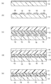
- Sectional drawing which showed two examples of the coverlay film concerning embodiment of this invention.
- the partial expanded sectional view which shows an example of the flexible wiring board concerning embodiment of this invention.
- Sectional drawing according to manufacturing process which shows an example of the manufacturing method of a flexible wiring board same as the above.
- the partially expanded sectional view which shows the other examples of the flexible wiring board concerning embodiment of this invention.
- FIGS. are schematic, and ratios of dimensions and the like are different from actual ones.
- the same or similar parts are denoted by the same reference numerals, and a duplicate description is partially omitted.
- the cover layer film of this embodiment has an adhesive layer 12 formed on one side (for example, the back side) of a film-like substrate 11.
- the adhesive layer 12 is an uncured thermosetting resin, and is adhered or formed on the film-like substrate 11 with an adhesive, for example.
- the mold release material layer 13 is further affixed on the back surface of the contact bonding layer 12.
- the film-like base material a resin film having a large elastic modulus as compared with the adhesive layer 12 after thermosetting and excellent in its low water absorption or low water absorption is preferable. With such a coverlay film, the change over time in its electrical characteristics is small and stable. Moreover, the adhesiveness with the base film in a flexible wiring board becomes stable and becomes excellent.
- the film-like substrate 11 is preferably a low dielectric resin film having low dielectric properties.
- the relative dielectric constant at a frequency of 1 GHz is preferably 3.5 or less.
- the dielectric loss tangent in the high frequency band is preferably 0.005 or less.
- the film thickness of the film-like substrate 11 is appropriately determined according to the FPC and material to which it is applied, and is set to about 5 ⁇ m to 50 ⁇ m, for example.
- the film-like substrate 11 is set to be relatively thick. This is to reduce the parasitic capacitance between the FPC wiring and the ground layer formed with the coverlay film interposed therebetween.
- a film-like substrate 11 examples include crystalline resins such as liquid crystal polymer, polyethylene naphthalate (PEN), syndiotactic polystyrene (SPS), polyphenylene sulfide (PPS), polyimide (PI) resin, and polyether.
- crystalline resins such as liquid crystal polymer, polyethylene naphthalate (PEN), syndiotactic polystyrene (SPS), polyphenylene sulfide (PPS), polyimide (PI) resin, and polyether.
- amorphous resins such as imide (PEI) and polyphenylene ether (PPE), and composite resins such as these.
- a thermosetting resin such as bismaleimide-triazine resin (BT resin) may be used.
- a liquid crystal polymer is preferable because it exhibits excellent high-frequency transmission characteristics and flexibility.
- the liquid crystal polymer is, for example, a multiaxially oriented thermoplastic polymer represented by xidar (trade name, manufactured by Dartco) or Vectra (trade name, manufactured by Clanese). Further, it may be modified by adding and blending another insulating resin. Examples include Bexter FA type (melting point 285 ° C.), Bexter CT-X type (melting point 280 ° C. to 335 ° C.), BIAC film (melting point 335 ° C.), and the like.
- the glass transition point Tg of these liquid crystal polymers exhibits a high temperature of 205 ° C. to 300 ° C.
- polyimide resin examples include polyimide film “Kapton” (trade name, manufactured by Toray DuPont) and Aurum (trade name, manufactured by Mitsui Chemicals). And as a polyethylene naphthalate type-resin, the thermoplastic resin of Teonex (brand name. Product made by Teijin DuPont) is illustrated as a suitable thing, for example.
- the adhesive layer 12 is a thermosetting synthetic resin containing an oligophenylene ether and a styrene butadiene elastomer.
- an ADFLEMA OPE system (trade name, manufactured by NAMICS) is exemplified as the uncured film.
- an adhesive prepared by appropriately dissolving or dispersing a component containing an oligophenylene ether or styrene butadiene elastomer in an organic solvent such as toluene can also be used.
- the film thickness of the adhesive layer 12 before thermosetting is appropriately determined according to the material of the film-like substrate 11, the material of the base film in the FPC, the thickness of the wiring formed on the base film, etc.
- This oligophenylene ether (including derivatives) is also called, for example, OPE (bifunctional polyphenylene ether oligomer) and has a polymer structure in which polyphenylene ether is added to both ends of the bifunctional core.
- OPE bifunctional polyphenylene ether oligomer
- the average molecular weight of OPE is about 500 to 5000, and preferably 1000 to 3000.
- Examples of such commercially available products include OPE2St-1200 and OPE2St-2200 manufactured by Mitsubishi Gas Chemical Company, Inc.
- the OPE is produced by using, for example, a vinyl compound described in JP2009-161725A and 2011-68713 as a composition.
- the adhesive layer 12 may contain other components.
- a maleimide-based curing agent, a phenol-based curing agent, an amine-based curing agent, and the like are appropriately mixed.
- an epoxy resin and its curing catalyst are added, for example.
- the curing catalyst for example, an amine-based curing catalyst or an imidazole-based curing catalyst for shortening heat curing is used.
- the adhesive layer 12 is made of a resin whose curing temperature is lower than the glass transition point Tg or the melting point Tm of the film-like substrate 11.
- the curing temperature is a temperature at which the uncured resin film or adhesive layer is cured by polymerization or crosslinking.
- the resin of the film-like substrate 11 may have a glass transition point and may not show a clear Tg. However, when the resin does not show a clear Tg, the thermosetting temperature is lower than the melting point Tm of the thermoplastic resin. Good. And the elasticity modulus in the contact bonding layer 12 after thermosetting becomes smaller than the elasticity modulus of the film-form base material 11 or the base film mentioned later.
- the elastic modulus in the adhesive layer 12 can be appropriately adjusted depending on the amount of the elastomer component.
- a resin having a small dielectric loss tangent such as polyester resin, nitrile rubber (NBR), styrene butadiene rubber (SBR), is preferable.
- the tensile elastic modulus of the adhesive layer 12 after thermosetting is set to be in the range of 100 MPa to 1 GPa.
- the tensile elastic modulus of the above-described film-like substrate 11 or base film is about 2 GPa to 20 GPa, which is larger than that of the adhesive layer 12.
- the glass transition point is usually determined by two methods, TMA method and DMA method, according to a glass transition temperature measurement method (according to JIS C-6493).
- TMA method the test piece is heated from room temperature at a rate of 10 ° C./min, the amount of thermal expansion in the thickness direction is measured with a thermal analyzer, and a tangent line is drawn on the curves before and after the glass transition point. Tg is obtained from the intersection of the tangent lines.
- the DMA method tensile method
- the test piece is heated from room temperature at a rate of 2 ° C./min, the dynamic viscoelasticity and loss tangent of the test piece are measured with a viscoelasticity measuring device, and the peak temperature of the loss tangent is measured.
- the elastic modulus the tensile elastic modulus or bending elastic modulus of the resin film is used. The elastic modulus is measured according to JIS K7127 or ASTM D882.
- the release material layer 13 is not particularly limited as long as it can be peeled without impairing the shape of the adhesive layer 12.
- Specific examples of the release material constituting the material include polypropylene (PP) film, polyethylene (PE) film, PP film with silicone release material, and PE film.
- the thickness of the release material layer 13 may be any thickness, but is 10 ⁇ m to 50 ⁇ m for a resin film and 50 ⁇ m to 100 ⁇ m for a release paper, for example.
- the inner layer signal wiring 15 and the ground wiring 16 which are a plurality of strip lines are arranged in a wiring pattern on one main surface of the base film 14 made of resin.
- the signal wiring 15 is shown as two pairs of transmission wirings that can cope with LVDS (Low Voltage Differential Signaling).
- the film-like base material 11 is thermocompression bonded to the signal wiring 15, the ground wiring 16, and the base film 14 through the adhesive layer 12 as a surface layer of the FPC, and is integrally formed.
- the film-like base material 11 and the adhesive layer 12 constitute a coverlay film.
- the elastic modulus of the adhesive layer 12 is smaller than the elastic moduli of the film-like substrate 11 and the base film 14 as described above.
- a ground layer may be stuck to the main surface facing the adhesive layer 12 via another adhesive layer.
- the other adhesive layer is made of the same resin as the adhesive layer 12.
- the cover dielectric film composed of the film-like substrate 11 and the adhesive layer 12 has a relative dielectric constant of 3 or less at 1 GHz. Further, their dielectric loss tangent is 0.003 or less. Further, the relative dielectric constant at 1 GHz including the base film 14 is all 3 or less. Similarly, the dielectric loss tangent at 1 GHz is 0.003 or less.
- the signal wiring 15 in this FPC exhibits extremely excellent transmission / conduction characteristics of a high-speed digital signal of 1 GHz or more, particularly several GHz to several tens GHz.
- thermoplastic resin or thermosetting resin having low dielectric properties can be used as the base film 14.
- cover lay film and the base film are made of the same material, the above-described characteristics are exhibited and the thermal expansion coefficient is the same, so that there is no inconvenience due to the coefficient difference.
- a single-sided copper-clad laminate in which a copper foil 17 is adhered to the surface of a base film 14 made of a liquid crystal polymer having a thickness of about 15 ⁇ m to 50 ⁇ m is prepared.
- the thickness of the copper foil 17 is about 3 ⁇ m to 35 ⁇ m.
- the single-sided copper-clad laminate may be one obtained by sticking a copper foil to the surface of a resin film, or one obtained by electrolytic plating.
- the copper foil 17 is patterned as a strip line by known etching to form the signal wiring 15 and the ground wiring 16.
- an uncured film-like adhesive layer 12 having a thickness of about 15 ⁇ m to 50 ⁇ m and a film-like substrate 11 made of a liquid crystal polymer having a thickness of about 5 ⁇ m to 50 ⁇ m, for example. are stacked in order from above the base film 14.
- a coverlay film composed of the adhesive layer 12 formed on one surface of the film-like substrate 11 may be overlapped.
- the laminated cushion sheet 18 is piled up on the film-form base material 11, and the film-form base material 11 is made into the base film 14 via the contact bonding layer 12 by the well-known hot roll laminating method.
- Thermocompression bonding is a predetermined temperature at which the adhesive layer 12 in an uncured state is cured, and is a temperature lower than the glass transition point or the melting point of the film-like substrate 11.
- the thermocompression bonding temperature is, for example, about 160 ° C. to 200 ° C.
- seat 18 is peeled and it heat-processes for a predetermined time at predetermined temperature, without pressing.
- This temperature is, for example, about 180 ° C. to 200 ° C.
- the film-like substrate 11 is joined and integrated with the base film 14, the signal wiring 15 and the ground wiring 16t via the adhesive layer 12.
- the flexible wiring board having the cross-sectional structure shown in FIG.
- the hot press method which is a heat press process similarly to the past.
- the required pressure is required for a predetermined time of about 1 to 2 hours, for example, by maintaining the predetermined temperature at which the adhesive layer 12 in an uncured state is cured.
- the base film 14, the signal wiring 15 and the ground wiring 16 and the coverlay film that are joined using the above-mentioned hot roll laminating method are joined together by roll-to-rolling using the flexibility of the base material in the manufacture of FPC.
- the roll (Roll to Roll) method is suitable for a production method using a long continuous substrate. In this method, for example, a flexible single-sided metal-clad laminate or a long-sided double-sided metal-clad laminate is used as a base material, and various processes are performed while being transported between a roll unwinder and a roll winder. It adds processing.
- the hot roll laminating method is suitable for the roll-to-roll method, while the hot press method is difficult to apply to the processing while transporting.
- the heat treatment for a predetermined time after the above-described hot roll laminating method is preferably performed separately from the roll-to-roll method in the final step.
- this roll-to-roll manufacturing method is suitable for manufacturing a long FPC with a length of 1 m or more, such as a flat cable on which transmission wiring is formed. Becomes effective.
- the adhesive layer 12 of the present embodiment has an elastic modulus after thermosetting that is smaller than the elastic modulus of the film-like substrate 11 or the base film 14, so that excellent bonding is possible. This is because the thermal stress generated when the temperature is lowered from the heated state to room temperature is absorbed and relaxed by the adhesive layer 12 regardless of the hot roll laminating method or the hot pressing method. That is, the adhesive layer 12 effectively functions as a cushioning material between the coverlay film and the base film to be joined because its elastic modulus is smaller than the surroundings.
- the heat-cured adhesive layer 12 has a low hygroscopic property and exhibits a stable value of a relative dielectric constant of 2.4 to 3.0 and a dielectric loss tangent of 0.0015 to 0.003. Further, the glass transition point has a high value of 180 ° C. to 230 ° C., for example.
- the amount of the adhesive layer 12 oozes out significantly compared to the case of the conventional adhesive layer. For this reason, the workability
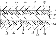
- FIG. 2 An FPC in which circuit wiring having a two-layer structure is provided.
- an FPC in which circuit wiring for transmitting a high-speed digital signal is formed will be described.
- a plurality of first circuit wirings 19 are arranged in a wiring pattern of, for example, a copper foil on one main surface of a base film 14 made of a resin such as a liquid crystal polymer.
- the first film-like substrate 20 is thermocompression bonded to the first circuit wiring 19 and the base film 14 via the first adhesive layer 21.
- the 1st film-like base material 20 and the 1st contact bonding layer 21 comprise a 1st coverlay film.
- a plurality of second circuit wirings 22 are arranged on another main surface of the base film 14 in, for example, another wiring pattern of copper foil.
- the second film-like base material 23 is thermocompression bonded to the second circuit wiring 19 and the base film 14 via the second adhesive layer 24.
- the 2nd film-like base material 23 and the 2nd contact bonding layer 24 comprise the 2nd coverlay film used as the surface layer of FPC.
- This second coverlay film is formed of the same or different material as the first coverlay film.
- the elastic modulus of the second adhesive layer 24 is set to be smaller than the elastic modulus of the second film-like substrate 23 and the base film 14. In this way, the FPC has a two-layer structure which is joined and integrated.
- a liquid crystal polymer is used for the first film-like substrate 11, the second film-like substrate 23, and the base film 14, and oligophenylene ether and styrene are used for the first adhesive layer 12 and the second adhesive layer 24. It is preferable to use a synthetic resin containing a butadiene-based elastomer.
- the signal wiring 15 in this FPC exhibits extremely excellent transmission / conduction characteristics of a high-speed digital signal in the range of several GHz to several tens of GHz. Then, for example, an FPC having a wiring circuit corresponding to a high-speed digital signal reaching the GHz band like a CPU clock of a computer is easily provided.
- a PI resin, a PEN resin, or a composite resin such as these is preferably used as the base film 14 in the two-layer structure FPC.
- a PI resin, a PEN resin, or a composite resin such as these is preferably used.
- other thermoplastic resins or thermosetting resins having low dielectric properties can be used.
- a multilayer wiring board having three or more layers of wiring can be formed in the same manner.
- a multilayer wiring board can be made very simply by laminating the FPC structure as shown in FIG. 1 or FIG. 4 with different adhesive layers sandwiched therebetween.
- a synthetic resin containing oligophenylene ether and a styrene-butadiene elastomer is used as in the case of the first adhesive layer 12 and the second adhesive layer 24.
- a resin such as a prepreg may be laminated between the multilayer wiring layers, and a coverlay film may be covered on the outermost layer as a surface layer to protect the inner layer wiring.
- the cover lay film of the present embodiment is composed of a film-like substrate, an adhesive layer made of a synthetic resin containing an oligophenylene ether and a styrene butadiene elastomer.
- the adhesive layer has an elastic modulus smaller than that of the film-like substrate.
- the film-like substrate has a low dielectric property, and its relative dielectric constant and dielectric loss tangent are preferably 3.5 or less and 0.005 or less, respectively.
- the adhesive layer used in this embodiment can easily reduce the elastic modulus, and exhibits stable and excellent adhesion of the coverlay film to the base film. And in manufacture of a flexible wiring board, the outstanding joining with a base film and wiring becomes easy. This is because in the thermocompression bonding using the hot roll laminating method or the hot pressing method as described above, the thermal stress generated when the temperature is lowered from the heated state to room temperature is absorbed and relaxed by the adhesive layer. .
- an adhesive that increases the relative dielectric constant and dielectric loss tangent as in the prior art may not be used in joining and integrating the base film and the wiring with the cover lay film.
- the combination of the base film and the coverlay film enables stable adhesion. And it becomes easy to make small the relative dielectric constant of the board
- the glass transition point of the adhesive layer is 180 ° C. or higher, and an FPC having high heat resistance and high bending resistance becomes possible. And it becomes possible to meet the demand for in-vehicle devices such as automobiles.
- the base film and the film-like substrate are preferably made of a liquid crystal polymer, a PI resin, or a PEN resin.
- the adhesive layer used in this embodiment can have a glass transition point of 230 ° C. or higher by adjusting the composition. For this reason, in mounting components such as semiconductor elements on a flexible wiring board, it is possible to realize a high heat resistance FPC that can endure even in a severe environment where lead-free solder reflow is performed at about 230 ° C., for example.
- the present invention is not limited to a flexible wiring board that transmits a high-frequency signal as described in the present embodiment.
- the present invention is similarly effective even in the case of an FPC that transmits a low-frequency electrical signal of less than 1 MHz.
- SYMBOLS 11 Film-like base material, 12 ... Adhesive layer, 13 ... Release material layer, 14 ... Base film, 15 ... Signal wiring, 16 ... Ground wiring, 17 ... Copper foil, 18 ... Laminated cushion sheet, 19 ... First circuit wiring 20 ... first film-like substrate, 21 ... first adhesive layer, 22 ... second circuit wiring, 23 ... second film-like substrate, 24 ... second adhesive layer
Landscapes
- Chemical & Material Sciences (AREA)
- Organic Chemistry (AREA)
- Engineering & Computer Science (AREA)
- Chemical Kinetics & Catalysis (AREA)
- Microelectronics & Electronic Packaging (AREA)
- Health & Medical Sciences (AREA)
- Manufacturing & Machinery (AREA)
- Medicinal Chemistry (AREA)
- Polymers & Plastics (AREA)
- Non-Metallic Protective Coatings For Printed Circuits (AREA)
- Adhesive Tapes (AREA)
- Adhesives Or Adhesive Processes (AREA)
- Manufacturing Of Printed Wiring (AREA)
- Structure Of Printed Boards (AREA)
Applications Claiming Priority (4)
| Application Number | Priority Date | Filing Date | Title |
|---|---|---|---|
| JP2011-285630 | 2011-12-27 | ||
| JP2011285630 | 2011-12-27 | ||
| JP2012-170818 | 2012-08-01 | ||
| JP2012170818A JP2013151638A (ja) | 2011-12-27 | 2012-08-01 | カバーレイフィルム、フレキシブル配線板およびその製造方法 |
Publications (1)
| Publication Number | Publication Date |
|---|---|
| WO2013099172A1 true WO2013099172A1 (ja) | 2013-07-04 |
Family
ID=48696718
Family Applications (1)
| Application Number | Title | Priority Date | Filing Date |
|---|---|---|---|
| PCT/JP2012/008166 Ceased WO2013099172A1 (ja) | 2011-12-27 | 2012-12-20 | カバーレイフィルム、フレキシブル配線板およびその製造方法 |
Country Status (2)
| Country | Link |
|---|---|
| JP (1) | JP2013151638A (enExample) |
| WO (1) | WO2013099172A1 (enExample) |
Cited By (4)
| Publication number | Priority date | Publication date | Assignee | Title |
|---|---|---|---|---|
| WO2014064986A1 (ja) * | 2012-10-24 | 2014-05-01 | ナミックス株式会社 | カバーレイフィルム、及びそれを用いたフレキシブルプリント配線板、並びにそれらの製造方法 |
| WO2016117282A1 (ja) * | 2015-01-19 | 2016-07-28 | パナソニックIpマネジメント株式会社 | 多層プリント配線板、多層金属張積層板、樹脂付き金属箔 |
| CN109414908A (zh) * | 2016-06-28 | 2019-03-01 | 株式会社斗山 | 附底漆铜箔及铜箔层叠板 |
| CN114656874A (zh) * | 2020-12-23 | 2022-06-24 | 日铁化学材料株式会社 | 聚酰亚胺组合物、树脂膜、层叠体、覆盖膜、带树脂的铜箔、覆金属层叠板及电路基板 |
Families Citing this family (20)
| Publication number | Priority date | Publication date | Assignee | Title |
|---|---|---|---|---|
| US9051465B1 (en) | 2012-02-21 | 2015-06-09 | Park Electrochemical Corporation | Thermosetting resin composition containing a polyphenylene ether and a brominated fire retardant compound |
| US9243164B1 (en) | 2012-02-21 | 2016-01-26 | Park Electrochemical Corporation | Thermosetting resin composition containing a polyphenylene ether and a brominated fire retardant compound |
| KR101549988B1 (ko) * | 2014-05-30 | 2015-09-03 | (주)창성 | 커버레이 분리형 자성시트와 이를 포함하는 연성인쇄회로기판 및 이들의 제조방법 |
| CN106063393B (zh) | 2015-02-16 | 2019-03-22 | 日本梅克特隆株式会社 | 柔性印刷布线板的制造方法 |
| JP2017092417A (ja) * | 2015-11-17 | 2017-05-25 | 信越ポリマー株式会社 | 電磁波シールドフィルムおよび電磁波シールドフィルム付きプリント配線板 |
| WO2017159788A1 (ja) * | 2016-03-17 | 2017-09-21 | 王子ホールディングス株式会社 | 粘着剤組成物及び粘着シート |
| WO2019230445A1 (ja) * | 2018-05-28 | 2019-12-05 | 東洋紡株式会社 | 低誘電接着剤組成物 |
| KR102753598B1 (ko) | 2018-09-06 | 2025-01-10 | 리껭테크노스 가부시키가이샤 | 핫멜트 접착제, 보강 테이프, 및 보강 테이프를 사용하여 도체 단말에서 보강된 플렉시블 플랫 케이블 |
| JP2020088271A (ja) * | 2018-11-29 | 2020-06-04 | 株式会社ジャパンディスプレイ | フレキシブル基板 |
| CN114174457B (zh) * | 2019-08-06 | 2023-08-25 | 迪睿合株式会社 | 粘接剂组合物、热固性粘接片以及印刷线路板 |
| WO2021025055A1 (ja) * | 2019-08-06 | 2021-02-11 | 株式会社村田製作所 | 樹脂多層基板および樹脂多層基板の製造方法 |
| KR20210018123A (ko) * | 2019-08-08 | 2021-02-17 | 스미또모 가가꾸 가부시키가이샤 | 적층체 |
| CN110677983A (zh) * | 2019-08-23 | 2020-01-10 | 李龙凯 | 一种高频线路板新型材料层结构的压合成型方法及其制品 |
| KR102390869B1 (ko) * | 2019-08-27 | 2022-04-26 | 주식회사 두산 | 커버레이 필름 및 이의 제조방법, 상기 커버레이 필름을 포함하는 연성 금속 복합기판 |
| KR102143318B1 (ko) * | 2020-04-29 | 2020-08-10 | 주식회사 두산 | 프라이머 코팅-동박 및 동박 적층판 |
| WO2022070899A1 (ja) * | 2020-09-29 | 2022-04-07 | 日東電工株式会社 | 粘着剤組成物、粘着剤層、及び粘着シート |
| JP2022056351A (ja) * | 2020-09-29 | 2022-04-08 | 日東電工株式会社 | 粘着剤組成物、粘着剤層、及び粘着シート |
| CN116209726A (zh) * | 2020-09-29 | 2023-06-02 | 日东电工株式会社 | 粘合剂组合物、粘合剂层及粘合片 |
| JP2022056352A (ja) * | 2020-09-29 | 2022-04-08 | 日東電工株式会社 | 粘着剤組成物、粘着剤層、及び粘着シート |
| KR102434919B1 (ko) * | 2022-04-01 | 2022-08-24 | 주식회사 노바텍 | 보호 케이스용 커버 부재의 제조방법 및 이에 의해 제조된 보호 케이스용 커버 부재 |
Citations (5)
| Publication number | Priority date | Publication date | Assignee | Title |
|---|---|---|---|---|
| JP2010050225A (ja) * | 2008-08-20 | 2010-03-04 | Sharp Corp | プリント配線板、プリント配線板製造方法、および電子機器 |
| JP2010219552A (ja) * | 2010-06-03 | 2010-09-30 | Nippon Mektron Ltd | 配線基板の製造方法 |
| JP2011040493A (ja) * | 2009-08-07 | 2011-02-24 | Namics Corp | 多層配線板、及び、多層配線板の製造方法 |
| JP2011068713A (ja) * | 2009-09-24 | 2011-04-07 | Namics Corp | カバーレイフィルム |
| WO2011111471A1 (ja) * | 2010-03-11 | 2011-09-15 | ナミックス株式会社 | フィルム用組成物、ならびに、それによる接着フィルムおよびカバーレイフィルム |
Family Cites Families (2)
| Publication number | Priority date | Publication date | Assignee | Title |
|---|---|---|---|---|
| US5234522A (en) * | 1990-12-05 | 1993-08-10 | Hitachi Chemical Company, Inc. | Method of producing flexible printed-circuit board covered with coverlay |
| JP2866779B2 (ja) * | 1993-01-05 | 1999-03-08 | 三井化学株式会社 | 耐熱性接着シート |
-
2012
- 2012-08-01 JP JP2012170818A patent/JP2013151638A/ja active Pending
- 2012-12-20 WO PCT/JP2012/008166 patent/WO2013099172A1/ja not_active Ceased
Patent Citations (5)
| Publication number | Priority date | Publication date | Assignee | Title |
|---|---|---|---|---|
| JP2010050225A (ja) * | 2008-08-20 | 2010-03-04 | Sharp Corp | プリント配線板、プリント配線板製造方法、および電子機器 |
| JP2011040493A (ja) * | 2009-08-07 | 2011-02-24 | Namics Corp | 多層配線板、及び、多層配線板の製造方法 |
| JP2011068713A (ja) * | 2009-09-24 | 2011-04-07 | Namics Corp | カバーレイフィルム |
| WO2011111471A1 (ja) * | 2010-03-11 | 2011-09-15 | ナミックス株式会社 | フィルム用組成物、ならびに、それによる接着フィルムおよびカバーレイフィルム |
| JP2010219552A (ja) * | 2010-06-03 | 2010-09-30 | Nippon Mektron Ltd | 配線基板の製造方法 |
Cited By (6)
| Publication number | Priority date | Publication date | Assignee | Title |
|---|---|---|---|---|
| WO2014064986A1 (ja) * | 2012-10-24 | 2014-05-01 | ナミックス株式会社 | カバーレイフィルム、及びそれを用いたフレキシブルプリント配線板、並びにそれらの製造方法 |
| WO2016117282A1 (ja) * | 2015-01-19 | 2016-07-28 | パナソニックIpマネジメント株式会社 | 多層プリント配線板、多層金属張積層板、樹脂付き金属箔 |
| JPWO2016117282A1 (ja) * | 2015-01-19 | 2017-11-02 | パナソニックIpマネジメント株式会社 | 多層プリント配線板、多層金属張積層板、樹脂付き金属箔 |
| US11818835B2 (en) | 2015-01-19 | 2023-11-14 | Panasonic Intellectual Property Management Co., Ltd. | Multilayer printed wiring board, multilayer metal-clad laminated board, and resin-coated metal foil |
| CN109414908A (zh) * | 2016-06-28 | 2019-03-01 | 株式会社斗山 | 附底漆铜箔及铜箔层叠板 |
| CN114656874A (zh) * | 2020-12-23 | 2022-06-24 | 日铁化学材料株式会社 | 聚酰亚胺组合物、树脂膜、层叠体、覆盖膜、带树脂的铜箔、覆金属层叠板及电路基板 |
Also Published As
| Publication number | Publication date |
|---|---|
| JP2013151638A (ja) | 2013-08-08 |
Similar Documents
| Publication | Publication Date | Title |
|---|---|---|
| WO2013099172A1 (ja) | カバーレイフィルム、フレキシブル配線板およびその製造方法 | |
| CN102480837B (zh) | 柔性布线板 | |
| JP3788917B2 (ja) | フレキシブル多層配線回路基板の製造方法 | |
| KR102082536B1 (ko) | 회로 기판 및 그 제조 방법 | |
| JP2015133474A (ja) | 電磁波シールドフィルム及びシールドフィルムを含む回路基板の作製方法 | |
| JP2013168643A (ja) | 電磁波シールドシートおよび電磁波シールド層付き配線板の製造方法 | |
| CN107791641B (zh) | 具有双层金属层的高遮蔽性电磁干扰屏蔽膜及其制备方法 | |
| CN106233825B (zh) | 印刷布线板 | |
| JP2013193253A (ja) | 電磁シールド性カバーレイフィルム、フレキシブル配線板およびその製造方法 | |
| CN101296562A (zh) | 铜箔基板以及利用该铜箔基板制作软性印刷电路板的方法 | |
| US11818835B2 (en) | Multilayer printed wiring board, multilayer metal-clad laminated board, and resin-coated metal foil | |
| CN108141967A (zh) | 配线基板的制造方法 | |
| TWI765306B (zh) | 具有高電磁屏蔽性能的軟性印刷電路板及其製備方法 | |
| KR100707056B1 (ko) | 폴리이미드계 연성 동박 적층판 및 그 제조 방법 | |
| WO2015014048A1 (zh) | 一种刚挠结合印制电路板及其制作方法 | |
| CN101296561B (zh) | 柔性印刷配线板及使用其的滑盖式移动电话终端 | |
| TWI302080B (enExample) | ||
| US20140186581A1 (en) | Primer-coated copper foil having superior adhesive strength and method for producing the same | |
| JPWO2020122071A1 (ja) | シールドプリント配線板の製造方法及びシールドプリント配線板 | |
| JP2014207297A (ja) | フレキシブルプリント回路及びその製造方法 | |
| JP2013149808A (ja) | メタルコアフレキシブル配線板およびその製造方法 | |
| CN111642068A (zh) | Rcc基板及多层叠置软板 | |
| CN114126202A (zh) | 一种覆铜基板及其制备方法、电路板、电子设备 | |
| JP2009278048A (ja) | シールド被覆フレキシブルプリント配線板の製造方法 | |
| KR101718855B1 (ko) | 전자파 차폐 및 방열용 복합 시트의 제조 방법 |
Legal Events
| Date | Code | Title | Description |
|---|---|---|---|
| 121 | Ep: the epo has been informed by wipo that ep was designated in this application |
Ref document number: 12861914 Country of ref document: EP Kind code of ref document: A1 |
|
| DPE1 | Request for preliminary examination filed after expiration of 19th month from priority date (pct application filed from 20040101) | ||
| NENP | Non-entry into the national phase |
Ref country code: DE |
|
| 122 | Ep: pct application non-entry in european phase |
Ref document number: 12861914 Country of ref document: EP Kind code of ref document: A1 |
|
| 122 | Ep: pct application non-entry in european phase |
Ref document number: 12861914 Country of ref document: EP Kind code of ref document: A1 |