WO2013094391A1 - 電子機器 - Google Patents
電子機器 Download PDFInfo
- Publication number
- WO2013094391A1 WO2013094391A1 PCT/JP2012/081241 JP2012081241W WO2013094391A1 WO 2013094391 A1 WO2013094391 A1 WO 2013094391A1 JP 2012081241 W JP2012081241 W JP 2012081241W WO 2013094391 A1 WO2013094391 A1 WO 2013094391A1
- Authority
- WO
- WIPO (PCT)
- Prior art keywords
- electronic device
- cover panel
- sound
- vibration element
- piezoelectric vibration
- Prior art date
- Legal status (The legal status is an assumption and is not a legal conclusion. Google has not performed a legal analysis and makes no representation as to the accuracy of the status listed.)
- Ceased
Links
Images


Classifications
-
- H—ELECTRICITY
- H04—ELECTRIC COMMUNICATION TECHNIQUE
- H04R—LOUDSPEAKERS, MICROPHONES, GRAMOPHONE PICK-UPS OR LIKE ACOUSTIC ELECTROMECHANICAL TRANSDUCERS; ELECTRIC HEARING AIDS; PUBLIC ADDRESS SYSTEMS
- H04R1/00—Details of transducers, loudspeakers or microphones
- H04R1/20—Arrangements for obtaining desired frequency or directional characteristics
- H04R1/22—Arrangements for obtaining desired frequency or directional characteristics for obtaining desired frequency characteristic only
- H04R1/28—Transducer mountings or enclosures modified by provision of mechanical or acoustic impedances, e.g. resonator, damping means
- H04R1/2869—Reduction of undesired resonances, i.e. standing waves within enclosure, or of undesired vibrations, i.e. of the enclosure itself
- H04R1/2884—Reduction of undesired resonances, i.e. standing waves within enclosure, or of undesired vibrations, i.e. of the enclosure itself by means of the enclosure structure, i.e. strengthening or shape of the enclosure
-
- H—ELECTRICITY
- H04—ELECTRIC COMMUNICATION TECHNIQUE
- H04R—LOUDSPEAKERS, MICROPHONES, GRAMOPHONE PICK-UPS OR LIKE ACOUSTIC ELECTROMECHANICAL TRANSDUCERS; ELECTRIC HEARING AIDS; PUBLIC ADDRESS SYSTEMS
- H04R1/00—Details of transducers, loudspeakers or microphones
- H04R1/02—Casings; Cabinets ; Supports therefor; Mountings therein
- H04R1/028—Casings; Cabinets ; Supports therefor; Mountings therein associated with devices performing functions other than acoustics, e.g. electric candles
-
- H—ELECTRICITY
- H04—ELECTRIC COMMUNICATION TECHNIQUE
- H04R—LOUDSPEAKERS, MICROPHONES, GRAMOPHONE PICK-UPS OR LIKE ACOUSTIC ELECTROMECHANICAL TRANSDUCERS; ELECTRIC HEARING AIDS; PUBLIC ADDRESS SYSTEMS
- H04R17/00—Piezoelectric transducers; Electrostrictive transducers
- H04R17/02—Microphones
-
- H—ELECTRICITY
- H04—ELECTRIC COMMUNICATION TECHNIQUE
- H04M—TELEPHONIC COMMUNICATION
- H04M1/00—Substation equipment, e.g. for use by subscribers
- H04M1/02—Constructional features of telephone sets
- H04M1/0202—Portable telephone sets, e.g. cordless phones, mobile phones or bar type handsets
-
- H—ELECTRICITY
- H04—ELECTRIC COMMUNICATION TECHNIQUE
- H04M—TELEPHONIC COMMUNICATION
- H04M1/00—Substation equipment, e.g. for use by subscribers
- H04M1/02—Constructional features of telephone sets
- H04M1/03—Constructional features of telephone transmitters or receivers, e.g. telephone hand-sets
- H04M1/035—Improving the acoustic characteristics by means of constructional features of the housing, e.g. ribs, walls, resonating chambers or cavities
-
- H—ELECTRICITY
- H04—ELECTRIC COMMUNICATION TECHNIQUE
- H04M—TELEPHONIC COMMUNICATION
- H04M1/00—Substation equipment, e.g. for use by subscribers
- H04M1/02—Constructional features of telephone sets
- H04M1/18—Telephone sets specially adapted for use in ships, mines, or other places exposed to adverse environment
-
- H—ELECTRICITY
- H04—ELECTRIC COMMUNICATION TECHNIQUE
- H04R—LOUDSPEAKERS, MICROPHONES, GRAMOPHONE PICK-UPS OR LIKE ACOUSTIC ELECTROMECHANICAL TRANSDUCERS; ELECTRIC HEARING AIDS; PUBLIC ADDRESS SYSTEMS
- H04R2499/00—Aspects covered by H04R or H04S not otherwise provided for in their subgroups
- H04R2499/10—General applications
- H04R2499/11—Transducers incorporated or for use in hand-held devices, e.g. mobile phones, PDA's, camera's
-
- H—ELECTRICITY
- H04—ELECTRIC COMMUNICATION TECHNIQUE
- H04R—LOUDSPEAKERS, MICROPHONES, GRAMOPHONE PICK-UPS OR LIKE ACOUSTIC ELECTROMECHANICAL TRANSDUCERS; ELECTRIC HEARING AIDS; PUBLIC ADDRESS SYSTEMS
- H04R2499/00—Aspects covered by H04R or H04S not otherwise provided for in their subgroups
- H04R2499/10—General applications
- H04R2499/15—Transducers incorporated in visual displaying devices, e.g. televisions, computer displays, laptops
Definitions
- the present invention relates to an electronic device that transmits sound to a user.
- Patent Document 1 a piezoelectric vibration element is attached to an outer surface of a casing of a telephone such as a mobile phone or a fixed telephone via an elastic member, and the piezoelectric vibration element is vibrated so that a user of the telephone
- a piezoelectric vibration element is vibrated so that a user of the telephone
- sound output from the electronic device may be input to a microphone provided in the electronic device and an acoustic echo may be generated.
- the present invention has been made in view of the above points, and an object thereof is to provide a technique capable of suppressing the generation of acoustic echoes in an electronic device.
- An electronic device configured to vibrate the piezoelectric vibration element based on a sound signal, a cover panel provided on a front surface of the electronic device, a piezoelectric vibration element provided on an inner main surface of the cover panel, and The electronic device is provided with a microphone hole in a portion other than the cover panel in the electronic device.
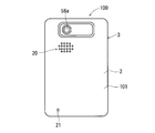
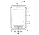
- FIGS. 1 to 3 are a perspective view, a front view, and a back view, respectively, showing an external appearance of the electronic device 100 according to the embodiment.
- Electronic device 100 according to the present embodiment is, for example, a mobile phone.
- the electronic device 100 includes a cover panel 1 and a case portion 2.
- a device case 3 having a substantially rectangular plate shape in plan view is configured.
- the cover panel 1 has a substantially rectangular shape in plan view.
- the cover panel 1 constitutes a part other than the peripheral part in the front part of the electronic device 100.
- the cover panel 1 is made of, for example, transparent glass or transparent acrylic resin.
- the case part 2 constitutes a peripheral part, a side part and a back part of the front part of the electronic device 100.
- the case portion 2 is made of, for example, polycarbonate resin.
- the cover panel 1 is provided with a display portion 1a on which various information such as characters, symbols and figures are displayed.
- the display portion 1a has, for example, a rectangular shape in plan view.
- the peripheral part 1b surrounding the display part 1a in the cover panel 1 is black, for example, by applying a film or the like, and is a non-display part where no information is displayed.
- a touch panel 53 described later is attached to the inner main surface of the cover panel 1. The user can give various instructions to the electronic device 100 by operating the display portion 1a of the cover panel 1 with a finger or the like.
- an operation unit 54 including a plurality of operation buttons 54a is provided.
- Each operation button 54a is a so-called “hard key”.
- the surface of each operation button 54 a is exposed from the lower end of the outer main surface 10 of the cover panel 1.
- a hole for exposing the plurality of operation buttons 54a is formed in the lower end portion of the cover panel 1.
- a piezoelectric vibration element 55 described later is provided inside the device case 3.
- a plurality of operation buttons 54a that are “hard keys” are provided.
- the number of the operation buttons 54a may be changed as appropriate, or the plurality of operation buttons 54a may be changed.
- the operation button 54a may not be provided.
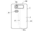
- a speaker hole 20 and a microphone hole 21 are formed on the back surface 101 of the electronic device 100, in other words, on the back surface of the device case 3.
- An imaging lens 58 a included in an imaging unit 58 described later is exposed from the back surface 101 of the electronic device 100.
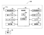
- FIG. 4 is a block diagram showing an electrical configuration of the electronic device 100.
- the electronic device 100 includes a control unit 50, a wireless communication unit 51, a display panel 52, a touch panel 53, an operation unit 54, a piezoelectric vibration element 55, an external speaker 56, a microphone 57, an imaging unit 58, and a battery. 59. These components of the electronic device 100 are housed in the device case 3.
- the control unit 50 includes a CPU 50a, a storage unit 50b, and the like.
- the control unit 50 comprehensively manages the operation of the electronic device 100 by controlling other components of the electronic device 100.
- the storage unit 50b includes a ROM, a RAM, and the like.
- Various functional blocks are formed in the control unit 50 when the CPU 50a executes various programs in the storage unit 50b.
- the wireless communication unit 51 receives a signal from a communication device such as a mobile phone different from the electronic device 100 or a web server connected to the Internet via the base station via the antenna 51a.
- the wireless communication unit 51 performs amplification processing and down-conversion on the received signal and outputs the result to the control unit 50.
- the control unit 50 performs demodulation processing or the like on the input reception signal, and acquires a sound signal indicating voice or music included in the reception signal.
- the wireless communication unit 51 performs up-conversion and amplification processing on the transmission signal including the sound signal generated by the control unit 50, and wirelessly transmits the processed transmission signal from the antenna 51a.
- a transmission signal from the antenna 51a is received through a base station by a mobile phone different from the electronic device 100 or a communication device connected to the Internet.
- the display panel 52 is, for example, a liquid crystal display panel or an organic EL panel, and displays various types of information such as characters, symbols, and figures by being controlled by the control unit 50.
- the information displayed on the display panel 52 is displayed on the display portion 1 a of the cover panel 1, so that the information can be visually recognized by the user of the electronic device 100.
- the touch panel 53 is, for example, a projected electrostatic capacity type touch panel.
- the touch panel 53 detects a user operation on the display portion 1 a of the cover panel 1.
- the touch panel 53 is affixed to the inner main surface of the cover panel 1.
- the touch panel 53 includes two sheet-like electrode sensors arranged to face each other. The two electrode sensors are bonded together with a transparent adhesive sheet.
- One electrode sensor is formed with a plurality of elongated X electrodes that extend along the X-axis direction (for example, the left-right direction of the electronic device 100) and are arranged in parallel to each other.
- the other electrode sensor is formed with a plurality of elongated Y electrodes that extend along the Y-axis direction (for example, the vertical direction of the electronic device 100) and are arranged in parallel to each other.
- the change in capacitance between the X electrode and the Y electrode that occurs in the touch panel 53 is transmitted to the control unit 50.
- the control unit 50 identifies the content of the operation performed on the display portion 1a of the cover panel 1 based on the capacitance change, and performs an operation corresponding thereto.
- the operation unit 54 outputs an operation signal indicating that the operation button 54a has been pressed to the control unit 50 when the operation button 54a is pressed by the user for each of the plurality of operation buttons 54a. Based on the input operation signal, the control unit 50 identifies which operation button 54a of the plurality of operation buttons 54a has been operated, and performs an operation according to the operated operation button 54a.
- the piezoelectric vibration element 55 is for transmitting the received sound to the user of the electronic device 100.
- the piezoelectric vibration element 55 is vibrated by a drive voltage supplied from the control unit 50.
- the control unit 50 generates a drive voltage based on the sound signal indicating the received sound, and applies the drive voltage to the piezoelectric vibration element 55.
- the piezoelectric vibration element 55 is vibrated by the control unit 50 based on the sound signal indicating the reception sound, whereby the reception sound is transmitted to the user of the electronic device 100.
- the control unit 50 functions as a drive unit that vibrates the piezoelectric vibration element 55 based on the sound signal.
- the piezoelectric vibration element 55 will be described in detail later.
- the external speaker 56 converts the electrical sound signal from the control unit 50 into sound and outputs the sound. Sound output from the external speaker 56 is output to the outside from the speaker hole 20 provided on the back surface 101 of the electronic device 100.
- the microphone 57 converts the sound input from the outside of the electronic device 100 into an electrical sound signal and outputs it to the control unit 50. Sound from the outside of the electronic device 100 is taken into the electronic device 100 through the microphone hole 21 provided on the back surface 101 of the electronic device 100 and input to the microphone 57.
- the imaging unit 58 includes an imaging lens 58a and an imaging element, and captures a still image and a moving image based on control by the control unit 50.
- the battery 59 outputs a power source for the electronic device 100.
- the power output from the battery 59 is supplied to each electronic component included in the control unit 50, the wireless communication unit 51, and the like included in the electronic device 100.
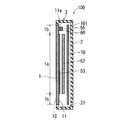
- ⁇ Details of piezoelectric vibration element> 5 and 6 are a top view and a side view showing the structure of the piezoelectric vibration element 55, respectively.
- the piezoelectric vibration element 55 has a long shape in one direction.
- the piezoelectric vibration element 55 has a rectangular elongated plate shape in plan view.
- the piezoelectric vibration element 55 has, for example, a bimorph structure, and includes a first piezoelectric ceramic plate 55a and a second piezoelectric ceramic plate 55b that are bonded to each other via a shim material 55c.
- the piezoelectric vibration element 55 when a positive voltage is applied to the first piezoelectric ceramic plate 55a and a negative voltage is applied to the second piezoelectric ceramic plate 55b, the first piezoelectric ceramic plate 55a extends along the longitudinal direction.
- the second piezoelectric ceramic plate 55b extends and contracts along the longitudinal direction. Accordingly, as shown in FIG. 7, the piezoelectric vibration element 55 bends in a mountain shape with the first piezoelectric ceramic plate 55a facing outside.
- the piezoelectric vibration element 55 when a negative voltage is applied to the first piezoelectric ceramic plate 55a and a positive voltage is applied to the second piezoelectric ceramic plate 55b, the first piezoelectric ceramic plate 55a is in the longitudinal direction.
- the second piezoelectric ceramic plate 55b extends along the longitudinal direction. Accordingly, as shown in FIG. 8, the piezoelectric vibration element 55 bends in a mountain shape with the second piezoelectric ceramic plate 55b facing outside.
- the piezoelectric vibration element 55 performs flexural vibration by alternately taking the state of FIG. 7 and the state of FIG.
- the controller 50 flexes and vibrates the piezoelectric vibration element 55 by applying an alternating voltage in which a positive voltage and a negative voltage appear alternately between the first piezoelectric ceramic plate 55a and the second piezoelectric ceramic plate 55b.
- the piezoelectric vibration element 55 shown in FIGS. 5 to 7 is provided with only one structure including the first piezoelectric ceramic plate 55a and the second piezoelectric ceramic plate 55b bonded with the shim material 55c interposed therebetween.
- the piezoelectric vibration element 55 may be configured by stacking a plurality of such structures.
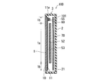
- FIG. 9 is a diagram illustrating a cross-sectional structure in the vertical direction (longitudinal direction) of the electronic device 100.
- FIG. 10 is a plan view of the cover panel 1 when viewed from the inner main surface 11 side.
- a touch panel 53 is attached to the inner main surface 11 of the cover panel 1 so as to face the display portion 1 a of the cover panel 1.
- the display panel 52 which is a display member is arrange
- the portion facing the display panel 52 is the display portion 1a.
- a printed circuit board 70 on which various components such as a CPU 50a and a microphone 57 are mounted is provided inside the device case 3.
- the printed circuit board 70 is disposed on the back surface 101 side of the electronic device 100 with respect to the display panel 52 so as to face the display panel 52.
- a plurality of holes 12 for exposing the plurality of operation buttons 54 a are formed in the lower end portion of the cover panel 1.
- the piezoelectric vibration element 55 is attached to the inner main surface 11 of the cover panel 1 with an adhesive 60 such as a double-sided tape.
- the piezoelectric vibration element 55 is disposed on the inner main surface 11 of the cover panel 1 at a position that does not overlap the display panel 52 and the touch panel 53 in a plan view when the cover panel 1 is viewed from the inner main surface 11 side.
- the piezoelectric vibration element 55 is arranged on the inner main surface 11 so as not to overlap the display panel 52 and the touch panel 53 when the cover panel 1 is viewed from the inner main surface 11 side in the thickness direction. ing. Therefore, the touch panel 53 and the display panel 52 do not exist between the cover panel 1 and the piezoelectric vibration element 55.
- the piezoelectric vibration element 55 is provided on the upper end 11 a of the inner main surface 11 of the cover panel 1. Specifically, as shown in FIG. 10, the piezoelectric vibration element 55 is located on the central portion 11aa in the left-right direction (short direction perpendicular to the longitudinal direction) of the upper end portion 11a of the inner main surface 11 of the cover panel 1. Is provided.
- the piezoelectric vibration element 55 is arranged so that the longitudinal direction thereof coincides with the left-right direction of the cover panel 1.
- the piezoelectric vibration element 55 is arranged at the center portion 11aa of the upper end portion 11a so that the longitudinal center thereof coincides with the center of the upper end portion 11a of the inner main surface 11 of the cover panel 1 in the left-right direction. Has been.
- the displacement amount is greatest at the center in the longitudinal direction. Therefore, by disposing the piezoelectric vibration element 55 at the upper end portion 11a so that the center in the longitudinal direction coincides with the center in the left-right direction of the upper end portion 11a of the inner main surface 11 of the cover panel 1. In the piezoelectric vibration element 55, the position where the displacement amount due to flexural vibration becomes maximum coincides with the center in the left-right direction of the upper end portion 11 a of the inner main surface 11 of the cover panel 1.
- the airway sound is a sound that is recognized by the human brain when sound waves (air vibrations) entering the ear canal hole (so-called “ear hole”) vibrate the eardrum.
- the conduction sound is sound that is recognized by the human brain when the auricle is vibrated and the vibration of the auricle is transmitted to the eardrum and the eardrum vibrates.
- the air conduction sound and the conduction sound will be described in detail.
- FIG. 11 is a diagram for explaining air conduction sound and conduction sound.
- FIG. 11 shows the structure of the ear of the user of electronic device 100.
- a wavy line 400 indicates a conduction path of a sound signal (sound information) when an airway sound is recognized by the brain.
- a solid line 410 indicates a conduction path of the sound signal when the conduction sound is recognized by the brain.
- the cover panel 1 vibrates and a sound wave is output from the cover panel 1.
- the cover panel 1 vibrates and a sound wave is output from the cover panel 1.
- the sound wave output from the cover panel 1 enters the ear canal hole 210. Sound waves from the cover panel 1 travel through the ear canal hole 210 and vibrate the eardrum 220.
- the vibration of the eardrum 220 is transmitted to the ossicle 230, and the ossicle 230 vibrates.
- the vibration of the ossicle 230 is transmitted to the cochlea 240 and converted into an electric signal in the cochlea 240.
- This electrical signal is transmitted to the brain through the auditory nerve 250, and the received sound is recognized in the brain. In this way, air conduction sound is transmitted from the cover panel 1 to the user.
- the auricle 200 is vibrated by the piezoelectric vibration element 55. It is vibrated by the cover panel 1.
- the vibration of the auricle 200 is transmitted to the eardrum 220, and the eardrum 220 vibrates.
- the vibration of the eardrum 220 is transmitted to the ossicle 230, and the ossicle 230 vibrates.
- the vibration of the ossicles 230 is transmitted to the cochlea 240 and converted into an electric signal in the cochlea 240.
- This electrical signal is transmitted to the brain through the auditory nerve 250, and the received sound is recognized in the brain. In this way, the conduction sound is transmitted from the cover panel 1 to the user.
- the auricular cartilage 200a inside the auricle 200 is also shown.
- Bone conduction sound is sound that is recognized by the human brain by vibrating the skull and directly stimulating the inner ear such as the cochlea.
- a sound signal transmission path when a bone conduction sound is recognized by the brain is indicated by a plurality of arcs 420.
- the piezoelectric vibration element 55 appropriately vibrates the front cover panel 1, in other words, the vibration of the piezoelectric vibration element 55 itself is appropriately applied to the front cover panel 1.
- the structure is devised so that air conduction sound and conduction sound can be appropriately transmitted to the user.
- Various merits are generated by configuring the electronic device 100 so that air conduction sound and conduction sound can be transmitted to the user.
- the user can hear a sound when the cover panel 1 is put on the ear, the user can make a call without worrying about the position of the electronic device 100 where the ear is put.
- the user can make the ambient noise difficult to hear while increasing the volume of the conduction sound by pressing the ear firmly against the cover panel 1. Therefore, the user can make a call appropriately even when the ambient noise is high.
- the user can recognize the received sound from the electronic device 100 by placing the cover panel 1 on the ear (more specifically, the auricle) even when the earplug or the earphone is attached to the ear. Can do. Further, the user can recognize the received sound from the electronic device 100 by applying the cover panel 1 to the headphones even when the headphones are attached to the ears.
- a gap is provided between the touch panel 53 and the display panel 52 as shown in FIG. 9, but the touch panel 53 and the display panel 52 may be brought into contact with each other.
- the cover panel 1 is pushed with a finger or the like by the user, and the cover panel 1 is bent toward the display panel 52 side.
- the display on the display panel 52 can be prevented from being disturbed when the cover panel 1 hits the display panel 52 (more precisely, the touch panel 53 hits the display panel 52).
- the piezoelectric vibration element is disposed on the inner main surface 11 of the cover panel 1 via the touch panel 53. 55 may be arranged.
- the touch panel 53 may not be provided on the electronic device 100, and input may be performed on the electronic device 100 using only hard keys.
- hard keys other than the operation buttons 54a may be further provided on the front surface of the electronic device 100 or the like.
- the cover panel 1 and the display panel 52 may be arranged to face each other with a space therebetween, or may be arranged to face each other and face each other.
- the piezoelectric vibration element 55 is on the inner main surface 11 of the cover panel 1 in a plan view when the cover panel 1 is viewed from the inner main surface 11 side. Since the display panel 52 is disposed so as not to overlap, the display panel 52 does not exist between the cover panel 1 and the piezoelectric vibration element 55. Therefore, it is possible to easily transmit the vibration of the piezoelectric vibration element 55 to the cover panel 1. Therefore, sound can be appropriately transmitted from the cover panel 1 to the user.
- the portion of the cover panel 1 that faces the display panel 52 that is, the display portion 1a is used. It is frequently pushed by a person with a finger or the like. When the cover panel 1 is pressed, the cover panel 1 may bend. Therefore, when the piezoelectric vibration element 55 is disposed in a portion of the cover panel 1 that is highly likely to be pressed by the user, the piezoelectric vibration. The element 55 may be damaged.
- the cover panel 1 is disposed at a position that does not overlap the display panel 52 in a plan view when viewed from the inner main surface 11 side.
- the piezoelectric vibration element 55 can be disposed in a portion of the cover panel 1 that is unlikely to be pressed because the cover panel 1 is disposed in a portion other than the display portion 1a. Therefore, it is possible to prevent the cover panel 1 from being pushed and the piezoelectric vibration element 55 from being damaged.
- the piezoelectric vibration element 55 is connected to the cover panel 1 as shown in FIG.
- the cover panel 1 and the piezoelectric vibration element 55 are arranged in a position where the cover panel 1 does not overlap the display panel 52 and the touch panel 53 in a plan view as viewed from the inner main surface 11 side.
- the touch panel 53 can be absent. Therefore, the vibration of the piezoelectric vibration element 55 can be more easily transmitted to the cover panel 1, and sound can be transmitted more appropriately from the cover panel 1 to the user.
- the piezoelectric device is used.
- the vibration element 55 is placed at the upper end portion of the inner main surface 11 of the cover panel 1.
- the piezoelectric vibration element 55 performs flexural vibration as in the present embodiment, the location where the displacement amount due to the flexural vibration in the piezoelectric vibration element 55 is maximized (the center in the longitudinal direction of the piezoelectric vibration element 55). ) And the center in the left-right direction at the upper end portion of the inner main surface 11 of the cover panel 1 can further increase the vibration at the center in the left-right direction at the upper end portion of the front surface of the cover panel 1. it can. As a result, the conduction sound can be more easily transmitted to the user.
- the longitudinal direction of the piezoelectric vibration element 55 is a cover panel as shown in FIGS. It is desirable that they are arranged so as to coincide with the left-right direction of 1.
- the piezoelectric vibration element 55 is disposed so that the longitudinal direction thereof coincides with the vertical direction of the cover panel 1, in order to prevent the display panel 52 from overlapping the piezoelectric vibration element 55, The position needs to be lowered. Therefore, it is necessary to lengthen the electronic device 100 in the up-down direction or to reduce the display portion 1a of the cover panel 1 in the up-down direction.
- the piezoelectric vibration element 55 is arranged so that the longitudinal direction thereof coincides with the left-right direction of the cover panel 1, thereby suppressing the length of the electronic device 100 in the up-down direction and covering the cover panel 1.
- the display portion 1a can be enlarged in the vertical direction.
- a hole is formed in the front cover panel to extract sound output from a receiver (receiver speaker) provided inside the electronic device to the outside of the electronic device. May be.
- the cover panel 1 that outputs sound does not have a hole in the earpiece (a hole for the receiver). That is, no earpiece hole is provided on the surface of the electronic device 100. Therefore, processing for making a hole in the earpiece in the cover panel 1 becomes unnecessary. As a result, the manufacturing cost of the electronic device 100 can be reduced, and the cost of the electronic device 100 can be reduced. In particular, when the cover panel 1 is made of glass, it is difficult to make a hole in the cover panel 1. Therefore, by not forming a hole in the earpiece in the cover panel 1, the manufacturing cost of the electronic device 100 can be reduced. Further reduction can be achieved.
- the strength of the cover panel 1 can be improved by not making a hole in the earpiece in the cover panel 1. Further, since the hole of the earpiece is not formed in the cover panel 1, the degree of freedom in design of the front surface of the cover panel 1 is improved. In particular, when the cover panel 1 occupies most of the front surface of the electronic device 100 as in the present embodiment, it is very effective from the viewpoint of design not to provide a hole for the earpiece in the cover panel 1. is there. Further, in the present embodiment, since there is no earpiece hole on the surface of electronic device 100, there is no problem of water or dust entering from the earpiece hole. Therefore, the electronic device 100 does not require a waterproof structure or a dust-proof structure for this problem, and the cost of the electronic device 100 can be further reduced.
- the reception sound is generated when the cover panel 1 vibrates, the reception sound can be appropriately transmitted to the user even if the electronic device 100 does not have a hole in the reception opening.
- the cover panel 1 has a hole 12 that exposes the operation button 54a.
- a hole that exposes the operation button 54a is formed in the case portion 2, and the hole 12 is formed in the cover panel 1. Need not be provided. Further, the operation button 54 a may be eliminated and the hole 12 may not be provided in the cover panel 1. As a result, there is no hole in the cover panel 1, and the cost of the electronic device 100 can be further reduced and the degree of freedom in design of the front surface of the cover panel 1 can be further improved.
- ⁇ About the position of the microphone hole> In an electronic device such as a mobile phone, sound generated by the electronic device (received sound in a mobile phone) may be input to a microphone to generate an acoustic echo.
- the microphone hole 21 In the electronic device 100, if the microphone hole 21 is temporarily formed in the cover panel 1, the microphone hole 21 is provided in a portion that outputs sound. Therefore, it is easy for sound to enter the microphone hole 21, and sound is easily input to the microphone 57. As a result, acoustic echo is likely to occur.
- the microphone hole 21 is provided in a portion other than the cover panel 1 that outputs sound, the position of the portion that outputs sound and the microphone in the electronic device 100 The position of the hole 21 can be separated. Therefore, it is possible to suppress the reception sound output from the cover panel 1 from being input to the microphone hole 21, and as a result, it is possible to suppress the generation of acoustic echoes.
- the microphone hole 21 is provided on the back surface 101 of the electronic device 100, but may be provided on the front surface or side surface of the electronic device 100 as long as it is a portion other than the cover panel 1.
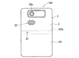
- FIG. 13 is a front view illustrating the electronic device 100 when the microphone hole 21 is provided in the case portion 2 on the front surface of the electronic device 100.
- FIG. 14 is a side view showing the electronic device 100 when the microphone hole 21 is provided in the case portion 2 on the side surface of the electronic device 100.
- the microphone hole 21 is provided on the lower side surface 102 (bottom surface) of the side surfaces of the electronic device 100.
- the microphone hole 21 is opened on the back surface 101 of the electronic device 100 as in the present embodiment. The generation of acoustic echo can be further suppressed.
- the microphone hole 21 may be formed in the central region 101 a along the vertical direction on the back surface 101 of the electronic device 100. Therefore, since the sound that wraps around the back surface 101 from the left-right direction of the electronic device 100 is less likely to enter the microphone hole 21, the generation of acoustic echoes can be further suppressed. Further, when the user holds the electronic device 100 with one hand and puts an ear on the cover panel 1 to make a call, the microphone hole 21 provided in the central region 101a is not easily blocked by the palm of the user. Therefore, it becomes easy to input the voice (speech sound) uttered by the user into the microphone 57.
- the microphone hole 21 may be formed in the central region 101 b along the left-right direction on the back surface 101 of the electronic device 100. Therefore, since the sound that wraps around the back surface 101 from the up-down direction of the electronic device 100 becomes difficult to enter the microphone hole 21, the generation of acoustic echoes can be further suppressed. Further, when the user holds the electronic device 100 with one hand and puts his ear on the cover panel 1 to make a call, the microphone hole 21 provided in the central region 101b is not easily blocked by the palm of the user. Therefore, it becomes easy to input the voice uttered by the user to the microphone 57.
- the microphone hole 21 is provided in the central portion 101 c of the back surface 101 of the electronic device 100 (a portion where the central region 101 a along the vertical direction and the central region 101 b along the horizontal direction overlap).
- the sound that wraps around the back surface 101 of the electronic device 100 is less likely to enter the microphone hole 21. Therefore, generation of acoustic echo can be further suppressed.
- the present invention can also be applied to an electronic device other than a mobile phone.
- the present invention can be applied to game machines, notebook personal computers, portable navigation systems, and the like.
Landscapes
- Physics & Mathematics (AREA)
- Engineering & Computer Science (AREA)
- Acoustics & Sound (AREA)
- Signal Processing (AREA)
- Health & Medical Sciences (AREA)
- Otolaryngology (AREA)
- Telephone Set Structure (AREA)
- Piezo-Electric Transducers For Audible Bands (AREA)
- Details Of Audible-Bandwidth Transducers (AREA)
- Telephone Function (AREA)
Priority Applications (1)
| Application Number | Priority Date | Filing Date | Title |
|---|---|---|---|
| US14/367,853 US9497536B2 (en) | 2011-12-22 | 2012-12-03 | Electronic device |
Applications Claiming Priority (2)
| Application Number | Priority Date | Filing Date | Title |
|---|---|---|---|
| JP2011-281542 | 2011-12-22 | ||
| JP2011281542A JP5926950B2 (ja) | 2011-12-22 | 2011-12-22 | 電子機器 |
Publications (1)
| Publication Number | Publication Date |
|---|---|
| WO2013094391A1 true WO2013094391A1 (ja) | 2013-06-27 |
Family
ID=48668290
Family Applications (1)
| Application Number | Title | Priority Date | Filing Date |
|---|---|---|---|
| PCT/JP2012/081241 Ceased WO2013094391A1 (ja) | 2011-12-22 | 2012-12-03 | 電子機器 |
Country Status (3)
| Country | Link |
|---|---|
| US (1) | US9497536B2 (https=) |
| JP (1) | JP5926950B2 (https=) |
| WO (1) | WO2013094391A1 (https=) |
Cited By (4)
| Publication number | Priority date | Publication date | Assignee | Title |
|---|---|---|---|---|
| WO2015012062A1 (ja) * | 2013-07-22 | 2015-01-29 | 京セラ株式会社 | 電子機器 |
| US9887724B2 (en) | 2014-12-25 | 2018-02-06 | Kyocera Corporation | Electronic apparatus |
| US10257954B2 (en) | 2015-07-28 | 2019-04-09 | Kyocera Corporation | Electronic device |
| US10347882B2 (en) | 2014-12-25 | 2019-07-09 | Kyocera Corporation | Electronic apparatus |
Families Citing this family (52)
| Publication number | Priority date | Publication date | Assignee | Title |
|---|---|---|---|---|
| CN108873372B (zh) | 2018-08-24 | 2024-06-14 | 深圳市韶音科技有限公司 | 一种铰链及眼镜 |
| JP5815612B2 (ja) | 2013-07-29 | 2015-11-17 | 京セラ株式会社 | 電子機器 |
| CN105378614B (zh) * | 2013-08-06 | 2019-05-21 | 株式会社村田制作所 | 按压检测传感器 |
| JP5952238B2 (ja) | 2013-08-28 | 2016-07-13 | 京セラ株式会社 | 電子機器 |
| JP5674895B1 (ja) | 2013-10-29 | 2015-02-25 | 京セラ株式会社 | 電子機器 |
| JP5865433B2 (ja) | 2013-11-27 | 2016-02-17 | 京セラ株式会社 | 電子機器 |
| JP5852635B2 (ja) | 2013-12-24 | 2016-02-03 | 京セラ株式会社 | 電子機器 |
| ES2724914T3 (es) * | 2013-12-25 | 2019-09-17 | Kyocera Corp | Dispositivo electrónico |
| US11974097B2 (en) | 2014-01-06 | 2024-04-30 | Shenzhen Shokz Co., Ltd. | Systems and methods for suppressing sound leakage |
| US11706574B2 (en) | 2014-01-06 | 2023-07-18 | Shenzhen Shokz Co., Ltd. | Systems and methods for suppressing sound leakage |
| US11617045B2 (en) | 2014-01-06 | 2023-03-28 | Shenzhen Shokz Co., Ltd. | Systems and methods for suppressing sound leakage |
| US11297446B2 (en) | 2014-01-06 | 2022-04-05 | Shenzhen Shokz Co., Ltd. | Systems and methods for suppressing sound leakage |
| CN106470371B (zh) | 2014-01-06 | 2018-02-27 | 深圳市韶音科技有限公司 | 一种能够抑制漏音的骨传导扬声器 |
| US11582565B2 (en) | 2014-01-06 | 2023-02-14 | Shenzhen Shokz Co., Ltd. | Systems and methods for suppressing sound leakage |
| US11418895B2 (en) | 2014-01-06 | 2022-08-16 | Shenzhen Shokz Co., Ltd. | Systems and methods for suppressing sound leakage |
| US11375324B2 (en) | 2014-01-06 | 2022-06-28 | Shenzhen Shokz Co., Ltd. | Systems and methods for suppressing sound leakage |
| US12457457B2 (en) | 2014-01-06 | 2025-10-28 | Shenzhen Shokz Co., Ltd. | Systems and methods for suppressing sound leakage |
| US11582563B2 (en) | 2014-01-06 | 2023-02-14 | Shenzhen Shokz Co., Ltd. | Systems and methods for suppressing sound leakage |
| US12483842B2 (en) | 2014-01-06 | 2025-11-25 | Shenzhen Shokz Co., Ltd. | Systems and methods for suppressing sound leakage |
| US11368801B2 (en) | 2014-01-06 | 2022-06-21 | Shenzhen Shokz Co., Ltd. | Systems and methods for suppressing sound leakage |
| US12538083B2 (en) | 2014-01-06 | 2026-01-27 | Shenzhen Shokz Co., Ltd. | Systems and methods for suppressing sound leakage |
| US12501224B2 (en) | 2014-01-06 | 2025-12-16 | Shenzhen Shokz Co., Ltd. | Systems and methods for suppressing sound leakage |
| US11570556B2 (en) | 2014-01-06 | 2023-01-31 | Shenzhen Shokz Co., Ltd. | Systems and methods for suppressing sound leakage |
| US12464299B2 (en) | 2014-01-06 | 2025-11-04 | Shenzhen Shokz Co., Ltd. | Systems and methods for suppressing sound leakage |
| US11589171B2 (en) | 2014-01-06 | 2023-02-21 | Shenzhen Shokz Co., Ltd. | Systems and methods for suppressing sound leakage |
| US11304011B2 (en) | 2014-01-06 | 2022-04-12 | Shenzhen Shokz Co., Ltd. | Systems and methods for suppressing sound leakage |
| US11368800B2 (en) | 2014-01-06 | 2022-06-21 | Shenzhen Shokz Co., Ltd. | Systems and methods for suppressing sound leakage |
| US11622209B2 (en) | 2014-01-06 | 2023-04-04 | Shenzhen Shokz Co., Ltd. | Systems and methods for suppressing sound leakage |
| US11805375B2 (en) | 2014-01-06 | 2023-10-31 | Shenzhen Shokz Co., Ltd. | Systems and methods for suppressing sound leakage |
| US12413915B2 (en) | 2014-01-06 | 2025-09-09 | Shenzhen Shokz Co., Ltd. | Systems and methods for suppressing sound leakage |
| US12581249B2 (en) | 2014-01-06 | 2026-03-17 | Shenzhen Shokz Co., Ltd. | Systems and methods for suppressing sound leakage |
| US12389172B2 (en) | 2014-01-06 | 2025-08-12 | Shenzhen Shokz Co., Ltd. | Systems and methods for suppressing sound leakage |
| US11363392B2 (en) | 2014-01-06 | 2022-06-14 | Shenzhen Shokz Co., Ltd. | Systems and methods for suppressing sound leakage |
| US12532132B2 (en) | 2014-01-06 | 2026-01-20 | Shenzhen Shokz Co., Ltd. | Systems and methods for suppressing sound leakage |
| US11627419B2 (en) | 2014-01-06 | 2023-04-11 | Shenzhen Shokz Co., Ltd. | Systems and methods for suppressing sound leakage |
| US11950055B2 (en) | 2014-01-06 | 2024-04-02 | Shenzhen Shokz Co., Ltd. | Systems and methods for suppressing sound leakage |
| US11558698B2 (en) | 2014-01-06 | 2023-01-17 | Shenzhen Shokz Co., Ltd. | Systems and methods for suppressing sound leakage |
| US12407992B2 (en) | 2014-01-06 | 2025-09-02 | Shenzhen Shokz Co., Ltd. | Systems and methods for suppressing sound leakage |
| WO2020220719A1 (zh) | 2019-04-30 | 2020-11-05 | 深圳市韶音科技有限公司 | 一种声学输出装置 |
| US11582564B2 (en) | 2014-01-06 | 2023-02-14 | Shenzhen Shokz Co., Ltd. | Systems and methods for suppressing sound leakage |
| US11197106B2 (en) * | 2014-01-06 | 2021-12-07 | Shenzhen Voxtech Co., Ltd. | Systems and methods for suppressing sound leakage |
| US11832060B2 (en) | 2014-01-06 | 2023-11-28 | Shenzhen Shokz Co., Ltd. | Systems and methods for suppressing sound leakage |
| JP6069237B2 (ja) | 2014-02-26 | 2017-02-01 | 京セラ株式会社 | 電子機器 |
| JP5865408B2 (ja) | 2014-02-26 | 2016-02-17 | 京セラ株式会社 | 電子機器 |
| JP6422685B2 (ja) | 2014-06-26 | 2018-11-14 | 京セラ株式会社 | 電子機器 |
| WO2016037332A1 (zh) * | 2014-09-11 | 2016-03-17 | 华为技术有限公司 | 一种移动终端 |
| JP6541988B2 (ja) | 2015-02-25 | 2019-07-10 | 京セラ株式会社 | 電子機器 |
| JP6467320B2 (ja) * | 2015-09-09 | 2019-02-13 | 日立オートモティブシステムズ株式会社 | 蓄電池制御装置 |
| US9655001B2 (en) * | 2015-09-24 | 2017-05-16 | Cisco Technology, Inc. | Cross mute for native radio channels |
| JP6143838B2 (ja) * | 2015-12-24 | 2017-06-07 | 京セラ株式会社 | 電子機器 |
| TWI637303B (zh) * | 2017-10-11 | 2018-10-01 | 聯陽半導體股份有限公司 | 觸控裝置及觸控裝置的操作方法 |
| WO2020038478A1 (zh) | 2018-08-24 | 2020-02-27 | 深圳市韶音科技有限公司 | 一种眼镜 |
Citations (5)
| Publication number | Priority date | Publication date | Assignee | Title |
|---|---|---|---|---|
| JPH06177809A (ja) * | 1992-12-11 | 1994-06-24 | Hitachi Ltd | 携帯用情報通信機器 |
| JP2002027063A (ja) * | 2000-07-07 | 2002-01-25 | Sony Corp | 携帯電話機 |
| JP2005236352A (ja) * | 2004-02-17 | 2005-09-02 | Authentic Ltd | 表示装置用パネル型スピーカ |
| JP2005348193A (ja) * | 2004-06-04 | 2005-12-15 | Nec Tokin Corp | 受話器 |
| JP2010162508A (ja) * | 2009-01-19 | 2010-07-29 | Authentic Ltd | 撓み振動型アクチュエータ |
Family Cites Families (22)
| Publication number | Priority date | Publication date | Assignee | Title |
|---|---|---|---|---|
| FR2777719B1 (fr) | 1998-04-20 | 2000-05-26 | Alsthom Cge Alcatel | Terminal de radiocommunication |
| JP2000013477A (ja) * | 1998-06-25 | 2000-01-14 | Kenwood Corp | 透明カバーの取り付け構造 |
| JP2002027036A (ja) * | 2000-07-04 | 2002-01-25 | Fujitsu I-Network Systems Ltd | 不在時着信情報表示機能付電話装置 |
| JP2002232542A (ja) | 2001-02-06 | 2002-08-16 | Taisei Plas Co Ltd | 携帯用通信機器 |
| JP4219732B2 (ja) | 2003-05-08 | 2009-02-04 | シチズン電子株式会社 | パネル型スピーカ付き表示端末装置 |
| DE602004005342D1 (de) | 2003-05-28 | 2007-04-26 | Koninkl Philips Electronics Nv | Als lautsprecher dienender anzeigeschirm |
| JP4133615B2 (ja) * | 2003-06-19 | 2008-08-13 | ポリマテック株式会社 | 小型音響素子のホルダ及びホルダの取付構造 |
| JP2005173194A (ja) * | 2003-12-11 | 2005-06-30 | Matsushita Electric Ind Co Ltd | 電子機器の表示装置 |
| JP2006166029A (ja) | 2004-12-07 | 2006-06-22 | Nec Saitama Ltd | 携帯型電子機器におけるフラットパネルスピーカの実装構造及び実装方法、並びに携帯型電子機器 |
| JP5169817B2 (ja) | 2006-03-07 | 2013-03-27 | 日本電気株式会社 | 圧電アクチュエータおよび電子機器 |
| US7612725B2 (en) | 2007-06-21 | 2009-11-03 | Apple Inc. | Antennas for handheld electronic devices with conductive bezels |
| JP5079873B2 (ja) | 2008-08-21 | 2012-11-21 | 日本写真印刷株式会社 | 表面フラット性に優れたタッチ入力機能付き保護パネル及び当該保護パネルを有する電子機器 |
| US20100117809A1 (en) * | 2008-11-11 | 2010-05-13 | Motorola Inc. | Display module with piezoelectric haptics |
| TWI381208B (zh) | 2008-12-16 | 2013-01-01 | 和碩聯合科技股份有限公司 | 顯示裝置 |
| US20110019354A1 (en) | 2009-03-02 | 2011-01-27 | Christopher Prest | Techniques for Strengthening Glass Covers for Portable Electronic Devices |
| JP5616907B2 (ja) * | 2009-03-02 | 2014-10-29 | アップル インコーポレイテッド | ポータブル電子デバイスのガラスカバーを強化する技術 |
| KR20110111031A (ko) * | 2010-04-02 | 2011-10-10 | 삼성전자주식회사 | 복합 터치 스크린 패널 장치 |
| US9313306B2 (en) * | 2010-12-27 | 2016-04-12 | Rohm Co., Ltd. | Mobile telephone cartilage conduction unit for making contact with the ear cartilage |
| JP5597583B2 (ja) * | 2011-03-28 | 2014-10-01 | 太陽誘電株式会社 | タッチパネル装置及び電子機器 |
| JP5676003B2 (ja) * | 2011-09-30 | 2015-02-25 | 京セラ株式会社 | 携帯電子機器 |
| JP2013141147A (ja) * | 2012-01-05 | 2013-07-18 | Kyocera Corp | 電子機器 |
| JP5681671B2 (ja) * | 2012-06-22 | 2015-03-11 | 京セラ株式会社 | 電子機器及び制御プログラム並びに情報通知方法 |
-
2011
- 2011-12-22 JP JP2011281542A patent/JP5926950B2/ja not_active Expired - Fee Related
-
2012
- 2012-12-03 WO PCT/JP2012/081241 patent/WO2013094391A1/ja not_active Ceased
- 2012-12-03 US US14/367,853 patent/US9497536B2/en active Active
Patent Citations (5)
| Publication number | Priority date | Publication date | Assignee | Title |
|---|---|---|---|---|
| JPH06177809A (ja) * | 1992-12-11 | 1994-06-24 | Hitachi Ltd | 携帯用情報通信機器 |
| JP2002027063A (ja) * | 2000-07-07 | 2002-01-25 | Sony Corp | 携帯電話機 |
| JP2005236352A (ja) * | 2004-02-17 | 2005-09-02 | Authentic Ltd | 表示装置用パネル型スピーカ |
| JP2005348193A (ja) * | 2004-06-04 | 2005-12-15 | Nec Tokin Corp | 受話器 |
| JP2010162508A (ja) * | 2009-01-19 | 2010-07-29 | Authentic Ltd | 撓み振動型アクチュエータ |
Cited By (4)
| Publication number | Priority date | Publication date | Assignee | Title |
|---|---|---|---|---|
| WO2015012062A1 (ja) * | 2013-07-22 | 2015-01-29 | 京セラ株式会社 | 電子機器 |
| US9887724B2 (en) | 2014-12-25 | 2018-02-06 | Kyocera Corporation | Electronic apparatus |
| US10347882B2 (en) | 2014-12-25 | 2019-07-09 | Kyocera Corporation | Electronic apparatus |
| US10257954B2 (en) | 2015-07-28 | 2019-04-09 | Kyocera Corporation | Electronic device |
Also Published As
| Publication number | Publication date |
|---|---|
| JP5926950B2 (ja) | 2016-05-25 |
| US9497536B2 (en) | 2016-11-15 |
| JP2013131987A (ja) | 2013-07-04 |
| US20150326967A1 (en) | 2015-11-12 |
Similar Documents
| Publication | Publication Date | Title |
|---|---|---|
| JP5926950B2 (ja) | 電子機器 | |
| US9332098B2 (en) | Electronic device with piezoelectric vibration element | |
| WO2013164906A1 (ja) | 電子機器 | |
| JP5674895B1 (ja) | 電子機器 | |
| JP5914426B2 (ja) | 電子機器 | |
| JP5815612B2 (ja) | 電子機器 | |
| JP6001508B2 (ja) | 電子機器 | |
| JP2013247625A (ja) | 電子機器 | |
| JP5952238B2 (ja) | 電子機器 | |
| JP5707454B2 (ja) | 電子機器 | |
| JP6219650B2 (ja) | 電子機器 | |
| JP5927105B2 (ja) | 電子機器 | |
| WO2013103025A1 (ja) | 電子機器 | |
| JP5865458B2 (ja) | 電子機器 | |
| JP6251306B2 (ja) | 電子機器 | |
| JP6302003B2 (ja) | 電子機器 | |
| JP6143838B2 (ja) | 電子機器 | |
| JP6154041B2 (ja) | 電子機器 | |
| JP5925874B2 (ja) | 電子機器 |
Legal Events
| Date | Code | Title | Description |
|---|---|---|---|
| 121 | Ep: the epo has been informed by wipo that ep was designated in this application |
Ref document number: 12859410 Country of ref document: EP Kind code of ref document: A1 |
|
| WWE | Wipo information: entry into national phase |
Ref document number: 14367853 Country of ref document: US |
|
| NENP | Non-entry into the national phase |
Ref country code: DE |
|
| 122 | Ep: pct application non-entry in european phase |
Ref document number: 12859410 Country of ref document: EP Kind code of ref document: A1 |