WO2013094391A1 - 電子機器 - Google Patents
電子機器 Download PDFInfo
- Publication number
- WO2013094391A1 WO2013094391A1 PCT/JP2012/081241 JP2012081241W WO2013094391A1 WO 2013094391 A1 WO2013094391 A1 WO 2013094391A1 JP 2012081241 W JP2012081241 W JP 2012081241W WO 2013094391 A1 WO2013094391 A1 WO 2013094391A1
- Authority
- WO
- WIPO (PCT)
- Prior art keywords
- electronic device
- cover panel
- sound
- vibration element
- piezoelectric vibration
- Prior art date
Links
- 230000005236 sound signal Effects 0.000 claims abstract description 14
- 239000000919 ceramic Substances 0.000 description 16
- 210000004556 brain Anatomy 0.000 description 10
- 210000003454 tympanic membrane Anatomy 0.000 description 8
- 238000004891 communication Methods 0.000 description 7
- 238000003384 imaging method Methods 0.000 description 6
- 230000004048 modification Effects 0.000 description 6
- 238000012986 modification Methods 0.000 description 6
- 210000003477 cochlea Anatomy 0.000 description 5
- 230000005540 biological transmission Effects 0.000 description 4
- 210000000988 bone and bone Anatomy 0.000 description 4
- 238000010586 diagram Methods 0.000 description 4
- 238000002592 echocardiography Methods 0.000 description 4
- 238000012545 processing Methods 0.000 description 4
- 238000013461 design Methods 0.000 description 3
- 238000006073 displacement reaction Methods 0.000 description 3
- 210000000613 ear canal Anatomy 0.000 description 3
- 230000002093 peripheral effect Effects 0.000 description 3
- 238000003860 storage Methods 0.000 description 3
- 239000000853 adhesive Substances 0.000 description 2
- 230000001070 adhesive effect Effects 0.000 description 2
- 230000003321 amplification Effects 0.000 description 2
- 230000008859 change Effects 0.000 description 2
- 238000006243 chemical reaction Methods 0.000 description 2
- 210000000860 cochlear nerve Anatomy 0.000 description 2
- 238000005516 engineering process Methods 0.000 description 2
- 239000011521 glass Substances 0.000 description 2
- 238000004519 manufacturing process Methods 0.000 description 2
- 239000000463 material Substances 0.000 description 2
- 238000003199 nucleic acid amplification method Methods 0.000 description 2
- 239000004925 Acrylic resin Substances 0.000 description 1
- 229920000178 Acrylic resin Polymers 0.000 description 1
- 239000000428 dust Substances 0.000 description 1
- 210000004728 ear cartilage Anatomy 0.000 description 1
- 210000003027 ear inner Anatomy 0.000 description 1
- 210000005069 ears Anatomy 0.000 description 1
- 239000004973 liquid crystal related substance Substances 0.000 description 1
- 210000004373 mandible Anatomy 0.000 description 1
- 238000000034 method Methods 0.000 description 1
- 229920005668 polycarbonate resin Polymers 0.000 description 1
- 239000004431 polycarbonate resin Substances 0.000 description 1
- 238000003825 pressing Methods 0.000 description 1
- 230000009467 reduction Effects 0.000 description 1
- 210000003625 skull Anatomy 0.000 description 1
- 230000004936 stimulating effect Effects 0.000 description 1
- XLYOFNOQVPJJNP-UHFFFAOYSA-N water Substances O XLYOFNOQVPJJNP-UHFFFAOYSA-N 0.000 description 1
Images


Classifications
-
- H—ELECTRICITY
- H04—ELECTRIC COMMUNICATION TECHNIQUE
- H04R—LOUDSPEAKERS, MICROPHONES, GRAMOPHONE PICK-UPS OR LIKE ACOUSTIC ELECTROMECHANICAL TRANSDUCERS; DEAF-AID SETS; PUBLIC ADDRESS SYSTEMS
- H04R1/00—Details of transducers, loudspeakers or microphones
- H04R1/20—Arrangements for obtaining desired frequency or directional characteristics
- H04R1/22—Arrangements for obtaining desired frequency or directional characteristics for obtaining desired frequency characteristic only
- H04R1/28—Transducer mountings or enclosures modified by provision of mechanical or acoustic impedances, e.g. resonator, damping means
- H04R1/2869—Reduction of undesired resonances, i.e. standing waves within enclosure, or of undesired vibrations, i.e. of the enclosure itself
- H04R1/2884—Reduction of undesired resonances, i.e. standing waves within enclosure, or of undesired vibrations, i.e. of the enclosure itself by means of the enclosure structure, i.e. strengthening or shape of the enclosure
-
- H—ELECTRICITY
- H04—ELECTRIC COMMUNICATION TECHNIQUE
- H04R—LOUDSPEAKERS, MICROPHONES, GRAMOPHONE PICK-UPS OR LIKE ACOUSTIC ELECTROMECHANICAL TRANSDUCERS; DEAF-AID SETS; PUBLIC ADDRESS SYSTEMS
- H04R1/00—Details of transducers, loudspeakers or microphones
- H04R1/02—Casings; Cabinets ; Supports therefor; Mountings therein
- H04R1/028—Casings; Cabinets ; Supports therefor; Mountings therein associated with devices performing functions other than acoustics, e.g. electric candles
-
- H—ELECTRICITY
- H04—ELECTRIC COMMUNICATION TECHNIQUE
- H04R—LOUDSPEAKERS, MICROPHONES, GRAMOPHONE PICK-UPS OR LIKE ACOUSTIC ELECTROMECHANICAL TRANSDUCERS; DEAF-AID SETS; PUBLIC ADDRESS SYSTEMS
- H04R17/00—Piezoelectric transducers; Electrostrictive transducers
- H04R17/02—Microphones
-
- H—ELECTRICITY
- H04—ELECTRIC COMMUNICATION TECHNIQUE
- H04M—TELEPHONIC COMMUNICATION
- H04M1/00—Substation equipment, e.g. for use by subscribers
- H04M1/02—Constructional features of telephone sets
- H04M1/0202—Portable telephone sets, e.g. cordless phones, mobile phones or bar type handsets
-
- H—ELECTRICITY
- H04—ELECTRIC COMMUNICATION TECHNIQUE
- H04M—TELEPHONIC COMMUNICATION
- H04M1/00—Substation equipment, e.g. for use by subscribers
- H04M1/02—Constructional features of telephone sets
- H04M1/03—Constructional features of telephone transmitters or receivers, e.g. telephone hand-sets
- H04M1/035—Improving the acoustic characteristics by means of constructional features of the housing, e.g. ribs, walls, resonating chambers or cavities
-
- H—ELECTRICITY
- H04—ELECTRIC COMMUNICATION TECHNIQUE
- H04M—TELEPHONIC COMMUNICATION
- H04M1/00—Substation equipment, e.g. for use by subscribers
- H04M1/02—Constructional features of telephone sets
- H04M1/18—Telephone sets specially adapted for use in ships, mines, or other places exposed to adverse environment
-
- H—ELECTRICITY
- H04—ELECTRIC COMMUNICATION TECHNIQUE
- H04R—LOUDSPEAKERS, MICROPHONES, GRAMOPHONE PICK-UPS OR LIKE ACOUSTIC ELECTROMECHANICAL TRANSDUCERS; DEAF-AID SETS; PUBLIC ADDRESS SYSTEMS
- H04R2499/00—Aspects covered by H04R or H04S not otherwise provided for in their subgroups
- H04R2499/10—General applications
- H04R2499/11—Transducers incorporated or for use in hand-held devices, e.g. mobile phones, PDA's, camera's
-
- H—ELECTRICITY
- H04—ELECTRIC COMMUNICATION TECHNIQUE
- H04R—LOUDSPEAKERS, MICROPHONES, GRAMOPHONE PICK-UPS OR LIKE ACOUSTIC ELECTROMECHANICAL TRANSDUCERS; DEAF-AID SETS; PUBLIC ADDRESS SYSTEMS
- H04R2499/00—Aspects covered by H04R or H04S not otherwise provided for in their subgroups
- H04R2499/10—General applications
- H04R2499/15—Transducers incorporated in visual displaying devices, e.g. televisions, computer displays, laptops
Definitions
- the present invention relates to an electronic device that transmits sound to a user.
- Patent Document 1 a piezoelectric vibration element is attached to an outer surface of a casing of a telephone such as a mobile phone or a fixed telephone via an elastic member, and the piezoelectric vibration element is vibrated so that a user of the telephone
- a piezoelectric vibration element is vibrated so that a user of the telephone
- sound output from the electronic device may be input to a microphone provided in the electronic device and an acoustic echo may be generated.
- the present invention has been made in view of the above points, and an object thereof is to provide a technique capable of suppressing the generation of acoustic echoes in an electronic device.
- An electronic device configured to vibrate the piezoelectric vibration element based on a sound signal, a cover panel provided on a front surface of the electronic device, a piezoelectric vibration element provided on an inner main surface of the cover panel, and The electronic device is provided with a microphone hole in a portion other than the cover panel in the electronic device.
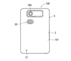
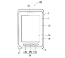
- FIGS. 1 to 3 are a perspective view, a front view, and a back view, respectively, showing an external appearance of the electronic device 100 according to the embodiment.
- Electronic device 100 according to the present embodiment is, for example, a mobile phone.
- the electronic device 100 includes a cover panel 1 and a case portion 2.
- a device case 3 having a substantially rectangular plate shape in plan view is configured.
- the cover panel 1 has a substantially rectangular shape in plan view.
- the cover panel 1 constitutes a part other than the peripheral part in the front part of the electronic device 100.
- the cover panel 1 is made of, for example, transparent glass or transparent acrylic resin.
- the case part 2 constitutes a peripheral part, a side part and a back part of the front part of the electronic device 100.
- the case portion 2 is made of, for example, polycarbonate resin.
- the cover panel 1 is provided with a display portion 1a on which various information such as characters, symbols and figures are displayed.
- the display portion 1a has, for example, a rectangular shape in plan view.
- the peripheral part 1b surrounding the display part 1a in the cover panel 1 is black, for example, by applying a film or the like, and is a non-display part where no information is displayed.
- a touch panel 53 described later is attached to the inner main surface of the cover panel 1. The user can give various instructions to the electronic device 100 by operating the display portion 1a of the cover panel 1 with a finger or the like.
- an operation unit 54 including a plurality of operation buttons 54a is provided.
- Each operation button 54a is a so-called “hard key”.
- the surface of each operation button 54 a is exposed from the lower end of the outer main surface 10 of the cover panel 1.
- a hole for exposing the plurality of operation buttons 54a is formed in the lower end portion of the cover panel 1.
- a piezoelectric vibration element 55 described later is provided inside the device case 3.
- a plurality of operation buttons 54a that are “hard keys” are provided.
- the number of the operation buttons 54a may be changed as appropriate, or the plurality of operation buttons 54a may be changed.
- the operation button 54a may not be provided.
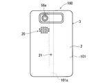
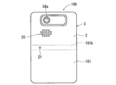
- a speaker hole 20 and a microphone hole 21 are formed on the back surface 101 of the electronic device 100, in other words, on the back surface of the device case 3.
- An imaging lens 58 a included in an imaging unit 58 described later is exposed from the back surface 101 of the electronic device 100.
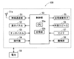
- FIG. 4 is a block diagram showing an electrical configuration of the electronic device 100.
- the electronic device 100 includes a control unit 50, a wireless communication unit 51, a display panel 52, a touch panel 53, an operation unit 54, a piezoelectric vibration element 55, an external speaker 56, a microphone 57, an imaging unit 58, and a battery. 59. These components of the electronic device 100 are housed in the device case 3.
- the control unit 50 includes a CPU 50a, a storage unit 50b, and the like.
- the control unit 50 comprehensively manages the operation of the electronic device 100 by controlling other components of the electronic device 100.
- the storage unit 50b includes a ROM, a RAM, and the like.
- Various functional blocks are formed in the control unit 50 when the CPU 50a executes various programs in the storage unit 50b.
- the wireless communication unit 51 receives a signal from a communication device such as a mobile phone different from the electronic device 100 or a web server connected to the Internet via the base station via the antenna 51a.
- the wireless communication unit 51 performs amplification processing and down-conversion on the received signal and outputs the result to the control unit 50.
- the control unit 50 performs demodulation processing or the like on the input reception signal, and acquires a sound signal indicating voice or music included in the reception signal.
- the wireless communication unit 51 performs up-conversion and amplification processing on the transmission signal including the sound signal generated by the control unit 50, and wirelessly transmits the processed transmission signal from the antenna 51a.
- a transmission signal from the antenna 51a is received through a base station by a mobile phone different from the electronic device 100 or a communication device connected to the Internet.
- the display panel 52 is, for example, a liquid crystal display panel or an organic EL panel, and displays various types of information such as characters, symbols, and figures by being controlled by the control unit 50.
- the information displayed on the display panel 52 is displayed on the display portion 1 a of the cover panel 1, so that the information can be visually recognized by the user of the electronic device 100.
- the touch panel 53 is, for example, a projected electrostatic capacity type touch panel.
- the touch panel 53 detects a user operation on the display portion 1 a of the cover panel 1.
- the touch panel 53 is affixed to the inner main surface of the cover panel 1.
- the touch panel 53 includes two sheet-like electrode sensors arranged to face each other. The two electrode sensors are bonded together with a transparent adhesive sheet.
- One electrode sensor is formed with a plurality of elongated X electrodes that extend along the X-axis direction (for example, the left-right direction of the electronic device 100) and are arranged in parallel to each other.
- the other electrode sensor is formed with a plurality of elongated Y electrodes that extend along the Y-axis direction (for example, the vertical direction of the electronic device 100) and are arranged in parallel to each other.
- the change in capacitance between the X electrode and the Y electrode that occurs in the touch panel 53 is transmitted to the control unit 50.
- the control unit 50 identifies the content of the operation performed on the display portion 1a of the cover panel 1 based on the capacitance change, and performs an operation corresponding thereto.
- the operation unit 54 outputs an operation signal indicating that the operation button 54a has been pressed to the control unit 50 when the operation button 54a is pressed by the user for each of the plurality of operation buttons 54a. Based on the input operation signal, the control unit 50 identifies which operation button 54a of the plurality of operation buttons 54a has been operated, and performs an operation according to the operated operation button 54a.
- the piezoelectric vibration element 55 is for transmitting the received sound to the user of the electronic device 100.
- the piezoelectric vibration element 55 is vibrated by a drive voltage supplied from the control unit 50.
- the control unit 50 generates a drive voltage based on the sound signal indicating the received sound, and applies the drive voltage to the piezoelectric vibration element 55.
- the piezoelectric vibration element 55 is vibrated by the control unit 50 based on the sound signal indicating the reception sound, whereby the reception sound is transmitted to the user of the electronic device 100.
- the control unit 50 functions as a drive unit that vibrates the piezoelectric vibration element 55 based on the sound signal.
- the piezoelectric vibration element 55 will be described in detail later.
- the external speaker 56 converts the electrical sound signal from the control unit 50 into sound and outputs the sound. Sound output from the external speaker 56 is output to the outside from the speaker hole 20 provided on the back surface 101 of the electronic device 100.
- the microphone 57 converts the sound input from the outside of the electronic device 100 into an electrical sound signal and outputs it to the control unit 50. Sound from the outside of the electronic device 100 is taken into the electronic device 100 through the microphone hole 21 provided on the back surface 101 of the electronic device 100 and input to the microphone 57.
- the imaging unit 58 includes an imaging lens 58a and an imaging element, and captures a still image and a moving image based on control by the control unit 50.
- the battery 59 outputs a power source for the electronic device 100.
- the power output from the battery 59 is supplied to each electronic component included in the control unit 50, the wireless communication unit 51, and the like included in the electronic device 100.
- ⁇ Details of piezoelectric vibration element> 5 and 6 are a top view and a side view showing the structure of the piezoelectric vibration element 55, respectively.
- the piezoelectric vibration element 55 has a long shape in one direction.
- the piezoelectric vibration element 55 has a rectangular elongated plate shape in plan view.
- the piezoelectric vibration element 55 has, for example, a bimorph structure, and includes a first piezoelectric ceramic plate 55a and a second piezoelectric ceramic plate 55b that are bonded to each other via a shim material 55c.
- the piezoelectric vibration element 55 when a positive voltage is applied to the first piezoelectric ceramic plate 55a and a negative voltage is applied to the second piezoelectric ceramic plate 55b, the first piezoelectric ceramic plate 55a extends along the longitudinal direction.
- the second piezoelectric ceramic plate 55b extends and contracts along the longitudinal direction. Accordingly, as shown in FIG. 7, the piezoelectric vibration element 55 bends in a mountain shape with the first piezoelectric ceramic plate 55a facing outside.
- the piezoelectric vibration element 55 when a negative voltage is applied to the first piezoelectric ceramic plate 55a and a positive voltage is applied to the second piezoelectric ceramic plate 55b, the first piezoelectric ceramic plate 55a is in the longitudinal direction.
- the second piezoelectric ceramic plate 55b extends along the longitudinal direction. Accordingly, as shown in FIG. 8, the piezoelectric vibration element 55 bends in a mountain shape with the second piezoelectric ceramic plate 55b facing outside.
- the piezoelectric vibration element 55 performs flexural vibration by alternately taking the state of FIG. 7 and the state of FIG.
- the controller 50 flexes and vibrates the piezoelectric vibration element 55 by applying an alternating voltage in which a positive voltage and a negative voltage appear alternately between the first piezoelectric ceramic plate 55a and the second piezoelectric ceramic plate 55b.
- the piezoelectric vibration element 55 shown in FIGS. 5 to 7 is provided with only one structure including the first piezoelectric ceramic plate 55a and the second piezoelectric ceramic plate 55b bonded with the shim material 55c interposed therebetween.
- the piezoelectric vibration element 55 may be configured by stacking a plurality of such structures.
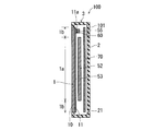
- FIG. 9 is a diagram illustrating a cross-sectional structure in the vertical direction (longitudinal direction) of the electronic device 100.
- FIG. 10 is a plan view of the cover panel 1 when viewed from the inner main surface 11 side.
- a touch panel 53 is attached to the inner main surface 11 of the cover panel 1 so as to face the display portion 1 a of the cover panel 1.
- the display panel 52 which is a display member is arrange
- the portion facing the display panel 52 is the display portion 1a.
- a printed circuit board 70 on which various components such as a CPU 50a and a microphone 57 are mounted is provided inside the device case 3.
- the printed circuit board 70 is disposed on the back surface 101 side of the electronic device 100 with respect to the display panel 52 so as to face the display panel 52.
- a plurality of holes 12 for exposing the plurality of operation buttons 54 a are formed in the lower end portion of the cover panel 1.
- the piezoelectric vibration element 55 is attached to the inner main surface 11 of the cover panel 1 with an adhesive 60 such as a double-sided tape.
- the piezoelectric vibration element 55 is disposed on the inner main surface 11 of the cover panel 1 at a position that does not overlap the display panel 52 and the touch panel 53 in a plan view when the cover panel 1 is viewed from the inner main surface 11 side.
- the piezoelectric vibration element 55 is arranged on the inner main surface 11 so as not to overlap the display panel 52 and the touch panel 53 when the cover panel 1 is viewed from the inner main surface 11 side in the thickness direction. ing. Therefore, the touch panel 53 and the display panel 52 do not exist between the cover panel 1 and the piezoelectric vibration element 55.
- the piezoelectric vibration element 55 is provided on the upper end 11 a of the inner main surface 11 of the cover panel 1. Specifically, as shown in FIG. 10, the piezoelectric vibration element 55 is located on the central portion 11aa in the left-right direction (short direction perpendicular to the longitudinal direction) of the upper end portion 11a of the inner main surface 11 of the cover panel 1. Is provided.
- the piezoelectric vibration element 55 is arranged so that the longitudinal direction thereof coincides with the left-right direction of the cover panel 1.
- the piezoelectric vibration element 55 is arranged at the center portion 11aa of the upper end portion 11a so that the longitudinal center thereof coincides with the center of the upper end portion 11a of the inner main surface 11 of the cover panel 1 in the left-right direction. Has been.
- the displacement amount is greatest at the center in the longitudinal direction. Therefore, by disposing the piezoelectric vibration element 55 at the upper end portion 11a so that the center in the longitudinal direction coincides with the center in the left-right direction of the upper end portion 11a of the inner main surface 11 of the cover panel 1. In the piezoelectric vibration element 55, the position where the displacement amount due to flexural vibration becomes maximum coincides with the center in the left-right direction of the upper end portion 11 a of the inner main surface 11 of the cover panel 1.
- the airway sound is a sound that is recognized by the human brain when sound waves (air vibrations) entering the ear canal hole (so-called “ear hole”) vibrate the eardrum.
- the conduction sound is sound that is recognized by the human brain when the auricle is vibrated and the vibration of the auricle is transmitted to the eardrum and the eardrum vibrates.
- the air conduction sound and the conduction sound will be described in detail.
- FIG. 11 is a diagram for explaining air conduction sound and conduction sound.
- FIG. 11 shows the structure of the ear of the user of electronic device 100.
- a wavy line 400 indicates a conduction path of a sound signal (sound information) when an airway sound is recognized by the brain.
- a solid line 410 indicates a conduction path of the sound signal when the conduction sound is recognized by the brain.
- the cover panel 1 vibrates and a sound wave is output from the cover panel 1.
- the cover panel 1 vibrates and a sound wave is output from the cover panel 1.
- the sound wave output from the cover panel 1 enters the ear canal hole 210. Sound waves from the cover panel 1 travel through the ear canal hole 210 and vibrate the eardrum 220.
- the vibration of the eardrum 220 is transmitted to the ossicle 230, and the ossicle 230 vibrates.
- the vibration of the ossicle 230 is transmitted to the cochlea 240 and converted into an electric signal in the cochlea 240.
- This electrical signal is transmitted to the brain through the auditory nerve 250, and the received sound is recognized in the brain. In this way, air conduction sound is transmitted from the cover panel 1 to the user.
- the auricle 200 is vibrated by the piezoelectric vibration element 55. It is vibrated by the cover panel 1.
- the vibration of the auricle 200 is transmitted to the eardrum 220, and the eardrum 220 vibrates.
- the vibration of the eardrum 220 is transmitted to the ossicle 230, and the ossicle 230 vibrates.
- the vibration of the ossicles 230 is transmitted to the cochlea 240 and converted into an electric signal in the cochlea 240.
- This electrical signal is transmitted to the brain through the auditory nerve 250, and the received sound is recognized in the brain. In this way, the conduction sound is transmitted from the cover panel 1 to the user.
- the auricular cartilage 200a inside the auricle 200 is also shown.
- Bone conduction sound is sound that is recognized by the human brain by vibrating the skull and directly stimulating the inner ear such as the cochlea.
- a sound signal transmission path when a bone conduction sound is recognized by the brain is indicated by a plurality of arcs 420.
- the piezoelectric vibration element 55 appropriately vibrates the front cover panel 1, in other words, the vibration of the piezoelectric vibration element 55 itself is appropriately applied to the front cover panel 1.
- the structure is devised so that air conduction sound and conduction sound can be appropriately transmitted to the user.
- Various merits are generated by configuring the electronic device 100 so that air conduction sound and conduction sound can be transmitted to the user.
- the user can hear a sound when the cover panel 1 is put on the ear, the user can make a call without worrying about the position of the electronic device 100 where the ear is put.
- the user can make the ambient noise difficult to hear while increasing the volume of the conduction sound by pressing the ear firmly against the cover panel 1. Therefore, the user can make a call appropriately even when the ambient noise is high.
- the user can recognize the received sound from the electronic device 100 by placing the cover panel 1 on the ear (more specifically, the auricle) even when the earplug or the earphone is attached to the ear. Can do. Further, the user can recognize the received sound from the electronic device 100 by applying the cover panel 1 to the headphones even when the headphones are attached to the ears.
- a gap is provided between the touch panel 53 and the display panel 52 as shown in FIG. 9, but the touch panel 53 and the display panel 52 may be brought into contact with each other.
- the cover panel 1 is pushed with a finger or the like by the user, and the cover panel 1 is bent toward the display panel 52 side.
- the display on the display panel 52 can be prevented from being disturbed when the cover panel 1 hits the display panel 52 (more precisely, the touch panel 53 hits the display panel 52).
- the piezoelectric vibration element is disposed on the inner main surface 11 of the cover panel 1 via the touch panel 53. 55 may be arranged.
- the touch panel 53 may not be provided on the electronic device 100, and input may be performed on the electronic device 100 using only hard keys.
- hard keys other than the operation buttons 54a may be further provided on the front surface of the electronic device 100 or the like.
- the cover panel 1 and the display panel 52 may be arranged to face each other with a space therebetween, or may be arranged to face each other and face each other.
- the piezoelectric vibration element 55 is on the inner main surface 11 of the cover panel 1 in a plan view when the cover panel 1 is viewed from the inner main surface 11 side. Since the display panel 52 is disposed so as not to overlap, the display panel 52 does not exist between the cover panel 1 and the piezoelectric vibration element 55. Therefore, it is possible to easily transmit the vibration of the piezoelectric vibration element 55 to the cover panel 1. Therefore, sound can be appropriately transmitted from the cover panel 1 to the user.
- the portion of the cover panel 1 that faces the display panel 52 that is, the display portion 1a is used. It is frequently pushed by a person with a finger or the like. When the cover panel 1 is pressed, the cover panel 1 may bend. Therefore, when the piezoelectric vibration element 55 is disposed in a portion of the cover panel 1 that is highly likely to be pressed by the user, the piezoelectric vibration. The element 55 may be damaged.
- the cover panel 1 is disposed at a position that does not overlap the display panel 52 in a plan view when viewed from the inner main surface 11 side.
- the piezoelectric vibration element 55 can be disposed in a portion of the cover panel 1 that is unlikely to be pressed because the cover panel 1 is disposed in a portion other than the display portion 1a. Therefore, it is possible to prevent the cover panel 1 from being pushed and the piezoelectric vibration element 55 from being damaged.
- the piezoelectric vibration element 55 is connected to the cover panel 1 as shown in FIG.
- the cover panel 1 and the piezoelectric vibration element 55 are arranged in a position where the cover panel 1 does not overlap the display panel 52 and the touch panel 53 in a plan view as viewed from the inner main surface 11 side.
- the touch panel 53 can be absent. Therefore, the vibration of the piezoelectric vibration element 55 can be more easily transmitted to the cover panel 1, and sound can be transmitted more appropriately from the cover panel 1 to the user.
- the piezoelectric device is used.
- the vibration element 55 is placed at the upper end portion of the inner main surface 11 of the cover panel 1.
- the piezoelectric vibration element 55 performs flexural vibration as in the present embodiment, the location where the displacement amount due to the flexural vibration in the piezoelectric vibration element 55 is maximized (the center in the longitudinal direction of the piezoelectric vibration element 55). ) And the center in the left-right direction at the upper end portion of the inner main surface 11 of the cover panel 1 can further increase the vibration at the center in the left-right direction at the upper end portion of the front surface of the cover panel 1. it can. As a result, the conduction sound can be more easily transmitted to the user.
- the longitudinal direction of the piezoelectric vibration element 55 is a cover panel as shown in FIGS. It is desirable that they are arranged so as to coincide with the left-right direction of 1.
- the piezoelectric vibration element 55 is disposed so that the longitudinal direction thereof coincides with the vertical direction of the cover panel 1, in order to prevent the display panel 52 from overlapping the piezoelectric vibration element 55, The position needs to be lowered. Therefore, it is necessary to lengthen the electronic device 100 in the up-down direction or to reduce the display portion 1a of the cover panel 1 in the up-down direction.
- the piezoelectric vibration element 55 is arranged so that the longitudinal direction thereof coincides with the left-right direction of the cover panel 1, thereby suppressing the length of the electronic device 100 in the up-down direction and covering the cover panel 1.
- the display portion 1a can be enlarged in the vertical direction.
- a hole is formed in the front cover panel to extract sound output from a receiver (receiver speaker) provided inside the electronic device to the outside of the electronic device. May be.
- the cover panel 1 that outputs sound does not have a hole in the earpiece (a hole for the receiver). That is, no earpiece hole is provided on the surface of the electronic device 100. Therefore, processing for making a hole in the earpiece in the cover panel 1 becomes unnecessary. As a result, the manufacturing cost of the electronic device 100 can be reduced, and the cost of the electronic device 100 can be reduced. In particular, when the cover panel 1 is made of glass, it is difficult to make a hole in the cover panel 1. Therefore, by not forming a hole in the earpiece in the cover panel 1, the manufacturing cost of the electronic device 100 can be reduced. Further reduction can be achieved.
- the strength of the cover panel 1 can be improved by not making a hole in the earpiece in the cover panel 1. Further, since the hole of the earpiece is not formed in the cover panel 1, the degree of freedom in design of the front surface of the cover panel 1 is improved. In particular, when the cover panel 1 occupies most of the front surface of the electronic device 100 as in the present embodiment, it is very effective from the viewpoint of design not to provide a hole for the earpiece in the cover panel 1. is there. Further, in the present embodiment, since there is no earpiece hole on the surface of electronic device 100, there is no problem of water or dust entering from the earpiece hole. Therefore, the electronic device 100 does not require a waterproof structure or a dust-proof structure for this problem, and the cost of the electronic device 100 can be further reduced.
- the reception sound is generated when the cover panel 1 vibrates, the reception sound can be appropriately transmitted to the user even if the electronic device 100 does not have a hole in the reception opening.
- the cover panel 1 has a hole 12 that exposes the operation button 54a.
- a hole that exposes the operation button 54a is formed in the case portion 2, and the hole 12 is formed in the cover panel 1. Need not be provided. Further, the operation button 54 a may be eliminated and the hole 12 may not be provided in the cover panel 1. As a result, there is no hole in the cover panel 1, and the cost of the electronic device 100 can be further reduced and the degree of freedom in design of the front surface of the cover panel 1 can be further improved.
- ⁇ About the position of the microphone hole> In an electronic device such as a mobile phone, sound generated by the electronic device (received sound in a mobile phone) may be input to a microphone to generate an acoustic echo.
- the microphone hole 21 In the electronic device 100, if the microphone hole 21 is temporarily formed in the cover panel 1, the microphone hole 21 is provided in a portion that outputs sound. Therefore, it is easy for sound to enter the microphone hole 21, and sound is easily input to the microphone 57. As a result, acoustic echo is likely to occur.
- the microphone hole 21 is provided in a portion other than the cover panel 1 that outputs sound, the position of the portion that outputs sound and the microphone in the electronic device 100 The position of the hole 21 can be separated. Therefore, it is possible to suppress the reception sound output from the cover panel 1 from being input to the microphone hole 21, and as a result, it is possible to suppress the generation of acoustic echoes.
- the microphone hole 21 is provided on the back surface 101 of the electronic device 100, but may be provided on the front surface or side surface of the electronic device 100 as long as it is a portion other than the cover panel 1.
- FIG. 13 is a front view illustrating the electronic device 100 when the microphone hole 21 is provided in the case portion 2 on the front surface of the electronic device 100.
- FIG. 14 is a side view showing the electronic device 100 when the microphone hole 21 is provided in the case portion 2 on the side surface of the electronic device 100.
- the microphone hole 21 is provided on the lower side surface 102 (bottom surface) of the side surfaces of the electronic device 100.
- the microphone hole 21 is opened on the back surface 101 of the electronic device 100 as in the present embodiment. The generation of acoustic echo can be further suppressed.
- the microphone hole 21 may be formed in the central region 101 a along the vertical direction on the back surface 101 of the electronic device 100. Therefore, since the sound that wraps around the back surface 101 from the left-right direction of the electronic device 100 is less likely to enter the microphone hole 21, the generation of acoustic echoes can be further suppressed. Further, when the user holds the electronic device 100 with one hand and puts an ear on the cover panel 1 to make a call, the microphone hole 21 provided in the central region 101a is not easily blocked by the palm of the user. Therefore, it becomes easy to input the voice (speech sound) uttered by the user into the microphone 57.
- the microphone hole 21 may be formed in the central region 101 b along the left-right direction on the back surface 101 of the electronic device 100. Therefore, since the sound that wraps around the back surface 101 from the up-down direction of the electronic device 100 becomes difficult to enter the microphone hole 21, the generation of acoustic echoes can be further suppressed. Further, when the user holds the electronic device 100 with one hand and puts his ear on the cover panel 1 to make a call, the microphone hole 21 provided in the central region 101b is not easily blocked by the palm of the user. Therefore, it becomes easy to input the voice uttered by the user to the microphone 57.
- the microphone hole 21 is provided in the central portion 101 c of the back surface 101 of the electronic device 100 (a portion where the central region 101 a along the vertical direction and the central region 101 b along the horizontal direction overlap).
- the sound that wraps around the back surface 101 of the electronic device 100 is less likely to enter the microphone hole 21. Therefore, generation of acoustic echo can be further suppressed.
- the present invention can also be applied to an electronic device other than a mobile phone.
- the present invention can be applied to game machines, notebook personal computers, portable navigation systems, and the like.
Landscapes
- Physics & Mathematics (AREA)
- Engineering & Computer Science (AREA)
- Acoustics & Sound (AREA)
- Signal Processing (AREA)
- Health & Medical Sciences (AREA)
- Otolaryngology (AREA)
- Telephone Set Structure (AREA)
- Piezo-Electric Transducers For Audible Bands (AREA)
- Details Of Audible-Bandwidth Transducers (AREA)
- Telephone Function (AREA)
Abstract
カバーパネルは、電子機器の前面に設けられている。圧電振動素子は、カバーパネルの内側主面上に設けられている。駆動部は、音信号に基づいて圧電振動素子を振動させる。電子機器における、カバーパネル以外の部分に、マイク穴が設けられている。
Description
本発明は、使用者に音を伝達する電子機器に関する。
従来から電子機器に関して様々な技術が提案されている。例えば特許文献1には、携帯電話機や固定電話機などの電話機の筐体の外面に対して弾性部材を介して圧電振動素子を取り付け、当該圧電振動素子を振動させることによって、当該電話機のユーザに対して音を伝達する技術が記載されている。
携帯電話機等の電子機器においては、当該電子機器が出力する音が、当該電子機器に設けられたマイクに入力されて、音響エコーが発生することがある。
そこで、本発明は上述の点に鑑みて成されたものであり、電子機器において音響エコーの発生を抑制することが可能な技術を提供することを目的とする。
ある態様に係る電子機器は、前記電子機器の前面に設けられたカバーパネルと、前記カバーパネルの内側主面上に設けられた圧電振動素子と、音信号に基づいて前記圧電振動素子を振動させる駆動部とを備え、前記電子機器における、前記カバーパネル以外の部分に、マイク穴が設けられている。
本発明によれば、音響エコーの発生を抑制することができる。
この発明の目的、特徴、局面、及び利点は、以下の詳細な説明と添付図面とによって、より明白となる。
<電子機器の外観>
図1~3は、それぞれ、実施の形態に係る電子機器100の外観を示す斜視図、前面図及び裏面図である。本実施の形態に係る電子機器100は、例えば携帯電話機である。
図1~3は、それぞれ、実施の形態に係る電子機器100の外観を示す斜視図、前面図及び裏面図である。本実施の形態に係る電子機器100は、例えば携帯電話機である。
図1に示されるように、電子機器100は、カバーパネル1とケース部分2を備えている。カバーパネル1とケース部分2とが組み合わされることによって、平面視で略長方形の板状を成す機器ケース3が構成されている。
カバーパネル1は、平面視において略長方形を成している。カバーパネル1は、電子機器100の前面部分における、周縁部分以外の部分を構成している。カバーパネル1は、例えば、透明のガラスあるいは透明のアクリル樹脂で形成されている。ケース部分2は、電子機器100の前面部分の周縁部分、側面部分及び裏面部分を構成している。ケース部分2は、例えばポリカーボネート樹脂で形成されている。
カバーパネル1には、文字、記号、図形等の各種情報が表示される表示部分1aが設けられている。表示部分1aは例えば平面視で長方形を成している。カバーパネル1における、表示部分1aを取り囲む周縁部分1bは、例えばフィルム等が貼られることによって黒色となっており、情報が表示されない非表示部分となっている。カバーパネル1の内側主面には後述するタッチパネル53が貼り付けられている。使用者は、カバーパネル1の表示部分1aを指等で操作することによって、電子機器100に対して各種指示を与えることができる。
機器ケース3の内部には、複数の操作ボタン54aを備える操作部54が設けられている。各操作ボタン54aは、いわゆる「ハードキー」である。各操作ボタン54aの表面は、カバーパネル1の外側主面10の下側端部から露出している。カバーパネル1の下側端部には、複数の操作ボタン54aを露出させるための穴があけられている。また、図2に示されるように、機器ケース3の内部には、後述する圧電振動素子55が設けられている。なお、本実施の形態に係る電子機器100では、「ハードキー」である複数の操作ボタン54aが設けられているが、当該複数の操作ボタン54aの個数を適宜変更しても良いし、当該複数の操作ボタン54aを設けなくても良い。
図3に示されるように、電子機器100の裏面101、言い換えれば機器ケース3の裏面には、スピーカ穴20及びマイク穴21があけられている。また電子機器100の裏面101からは、後述する撮像部58が有する撮像レンズ58aが露出している。
<電子機器の電気的構成>
図4は電子機器100の電気的構成を示すブロック図である。図4に示されるように、電子機器100は、制御部50、無線通信部51、表示パネル52、タッチパネル53、操作部54、圧電振動素子55、外部スピーカ56、マイク57、撮像部58及び電池59を備えている。電子機器100のこれらの構成要素は、機器ケース3内に収められている。
図4は電子機器100の電気的構成を示すブロック図である。図4に示されるように、電子機器100は、制御部50、無線通信部51、表示パネル52、タッチパネル53、操作部54、圧電振動素子55、外部スピーカ56、マイク57、撮像部58及び電池59を備えている。電子機器100のこれらの構成要素は、機器ケース3内に収められている。
制御部50は、CPU50a及び記憶部50b等を備えている。制御部50は、電子機器100の他の構成要素を制御することによって、電子機器100の動作を統括的に管理する。記憶部50bは、ROM及びRAM等で構成されている。制御部50には、CPU50aが記憶部50b内の各種プログラムを実行することによって、様々な機能ブロックが形成される。
無線通信部51は、電子機器100とは別の携帯電話機あるいはインターネットに接続されたウェブサーバ等の通信装置からの信号を基地局を介してアンテナ51aで受信する。無線通信部51は、受信信号に対して増幅処理及びダウンコンバートを行って制御部50に出力する。制御部50は、入力される受信信号に対して復調処理等を行って、当該受信信号に含まれる、音声や音楽などを示す音信号などを取得する。また無線通信部51は、制御部50で生成された、音信号等を含む送信信号に対してアップコンバート及び増幅処理を行って、処理後の送信信号をアンテナ51aから無線送信する。アンテナ51aからの送信信号は、基地局を通じて、電子機器100とは別の携帯電話機あるいはインターネットに接続された通信装置で受信される。
表示パネル52は、例えば、液晶表示パネルあるいは有機ELパネルであって、制御部50によって制御されることによって、文字、記号、図形などの各種情報を表示する。表示パネル52に表示される情報は、カバーパネル1の表示部分1aに表示されることによって、当該情報は電子機器100の使用者に視認可能となる。
タッチパネル53は、例えば、投影型静電量容量方式のタッチパネルである。タッチパネル53は、カバーパネル1の表示部分1aに対する使用者の操作を検出する。タッチパネル53は、カバーパネル1の内側主面に貼り付けられている。タッチパネル53は、互いに対向配置されたシート状の2つの電極センサーを備えている。2つの電極センサーは透明粘着性シートによって貼り合わされている。
一方の電極センサーには、それぞれがX軸方向(例えば電子機器100の左右方向)に沿って延在し、かつ互いに平行に配置された複数の細長いX電極が形成されている。他方の電極センサーには、それぞれがY軸方向(例えば電子機器100の上下方向)に沿って延在し、かつ互いに平行に配置された複数の細長いY電極が形成されている。カバーパネル1の表示部分1aに対して使用者の指が接触すると、その接触箇所の下にあるX電極及びY電極の間の静電容量が変化することによって、タッチパネル53においてカバーパネル1の表示部分1aに対する操作が検出される。タッチパネル53において生じる、X電極及びY電極の間の静電容量変化は制御部50に伝達される。制御部50は当該静電容量変化に基づいてカバーパネル1の表示部分1aに対して行われた操作の内容を特定し、それに応じた動作を行う。
操作部54は、複数の操作ボタン54aのそれぞれについて、当該操作ボタン54aが使用者によって押下されると、当該操作ボタン54aが押下されたことを示す操作信号を制御部50に出力する。制御部50は、入力される操作信号に基づいて、複数の操作ボタン54aのうちのどの操作ボタン54aが操作されたかを特定し、操作された操作ボタン54aに応じた動作を行う。
圧電振動素子55は、受話音を電子機器100の使用者に伝えるためのものである。圧電振動素子55は、制御部50から与えられる駆動電圧によって振動させられる。制御部50は、受話音を示す音信号に基づいて駆動電圧を生成し、当該駆動電圧を圧電振動素子55に印加する。圧電振動素子55が、制御部50によって受話音を示す音信号に基づいて振動させられることによって、電子機器100の使用者には受話音が伝達される。このように、制御部50は、音信号に基づいて圧電振動素子55を振動させる駆動部として機能する。圧電振動素子55については後で詳細に説明する。
外部スピーカ56は、制御部50からの電気的な音信号を音に変換して出力する。外部スピーカ56から出力される音は、電子機器100の裏面101に設けられたスピーカ穴20から外部に出力される。
マイク57は、電子機器100の外部から入力される音を電気的な音信号に変換して制御部50に出力する。電子機器100の外部からの音は、当該電子機器100の裏面101に設けられたマイク穴21から当該電子機器100の内部に取り込まれて、マイク57に入力される。
撮像部58は、撮像レンズ58a及び撮像素子などで構成されており、制御部50による制御に基づいて、静止画像及び動画像を撮像する。
電池59は、電子機器100の電源を出力する。電池59から出力された電源は、電子機器100が備える制御部50や無線通信部51などに含まれる各電子部品に対して供給される。
<圧電振動素子の詳細>
図5,6は、それぞれ、圧電振動素子55の構造を示す上面図及び側面図である。図5,6に示されるように、圧電振動素子55は一方向に長い形状を成している。具体的には、圧電振動素子55は、平面視で長方形の細長い板状を成している。圧電振動素子55は、例えばバイモルフ構造を有しており、シム材55cを介して互いに貼り合わされた第1圧電セラミック板55a及び第2圧電セラミック板55bを備えている。
図5,6は、それぞれ、圧電振動素子55の構造を示す上面図及び側面図である。図5,6に示されるように、圧電振動素子55は一方向に長い形状を成している。具体的には、圧電振動素子55は、平面視で長方形の細長い板状を成している。圧電振動素子55は、例えばバイモルフ構造を有しており、シム材55cを介して互いに貼り合わされた第1圧電セラミック板55a及び第2圧電セラミック板55bを備えている。
圧電振動素子55では、第1圧電セラミック板55aに対して正の電圧を印加し、第2圧電セラミック板55bに対して負の電圧を印加すると、第1圧電セラミック板55aは長手方向に沿って伸び、第2圧電セラミック板55bは長手方向に沿って縮むようになる。これにより、図7に示されるように、圧電振動素子55は、第1圧電セラミック板55aを外側にして山状に撓むようになる。
一方で、圧電振動素子55では、第1圧電セラミック板55aに対して負の電圧を印加し、第2圧電セラミック板55bに対して正の電圧を印加すると、第1圧電セラミック板55aは長手方向に沿って縮み、第2圧電セラミック板55bは長手方向に沿って伸びるようになる。これにより、図8に示されるように、圧電振動素子55は、第2圧電セラミック板55bを外側にして山状に撓むようになる。
圧電振動素子55は、図7の状態と図8の状態とを交互にとることによって、撓み振動を行う。制御部50は、第1圧電セラミック板55aと第2圧電セラミック板55bとの間に、正の電圧と負の電圧とが交互に現れる交流電圧を印加することによって、圧電振動素子55を撓み振動させる。
なお、図5~7に示される圧電振動素子55では、シム材55cを間に挟んで貼り合わされた第1圧電セラミック板55a及び第2圧電セラミック板55bから成る構造が一つだけ設けられていたが、複数の当該構造を積層させて圧電振動素子55を構成しても良い。
<圧電振動素子の配置位置>
図9は電子機器100の上下方向(長手方向)における断面構造を示す図である。また図10は、カバーパネル1をその内側主面11側から見た際の平面図である。
図9は電子機器100の上下方向(長手方向)における断面構造を示す図である。また図10は、カバーパネル1をその内側主面11側から見た際の平面図である。
図9,10に示されるように、カバーパネル1の内側主面11には、当該カバーパネル1の表示部分1aと対向するようにタッチパネル53が貼り付けられている。そして、表示部材である表示パネル52は、カバーパネル1及びタッチパネル53に対向するように配置されている。したがって、カバーパネル1と表示パネル52との間にはタッチパネル53が存在している。カバーパネル1では、表示パネル52と対向している部分が表示部分1aとなる。
また、機器ケース3の内部には、CPU50a及びマイク57などの各種部品が搭載されるプリント基板70が設けられている。プリント基板70は、表示パネル52よりも電子機器100の裏面101側において当該表示パネル52と対向するように配置されている。また、図10に示されるように、カバーパネル1の下側端部には、複数の操作ボタン54aをそれぞれ露出させる複数の穴12があけられている。
圧電振動素子55は、両面テープ等の接着剤60によって、カバーパネル1の内側主面11に貼り付けられている。圧電振動素子55は、カバーパネル1の内側主面11上において、当該カバーパネル1を当該内側主面11側から見た平面視で表示パネル52及びタッチパネル53とは重ならない位置に配置されている。言い換えれば、圧電振動素子55は、カバーパネル1をその厚み方向において内側主面11側から見た際に、当該内側主面11上において、表示パネル52及びタッチパネル53とは重ならない位置に配置されている。したがって、カバーパネル1と圧電振動素子55との間には、タッチパネル53及び表示パネル52は存在していない。
また、圧電振動素子55は、カバーパネル1の内側主面11の上側端部11a上に設けられている。具体的には、圧電振動素子55は、図10に示されるように、カバーパネル1の内側主面11の上側端部11aにおける左右方向(長手方向に垂直な短手方向)の中央部11aa上に設けられている。
また、圧電振動素子55は、その長手方向がカバーパネル1の左右方向に一致するように配置されている。そして、圧電振動素子55は、その長手方向の中心が、カバーパネル1の内側主面11の上側端部11aにおける左右方向の中心と一致するように、当該上側端部11aの中央部11aaに配置されている。
ここで、上述の図7,8に示されるように、撓み振動を行う圧電振動素子55では、その長手方向の中心が最も変位量が大きくなる。したがって、圧電振動素子55を、その長手方向の中心が、カバーパネル1の内側主面11の上側端部11aにおける左右方向の中心と一致するように、当該上側端部11aに配置することによって、圧電振動素子55における、撓み振動での変位量が最大となる箇所が、カバーパネル1の内側主面11の上側端部11aにおける左右方向の中心に一致するようになる。
<圧電振動素子の振動による受話音の発生について>
本実施の形態では、圧電振動素子55がカバーパネル1を振動させることによって、当該カバーパネル1から気導音及び伝導音が使用者に伝達されるようになっている。言い換えれば、圧電振動素子55自身の振動がカバーパネル1に伝わることにより、当該カバーパネル1から気導音及び伝導音が使用者に伝達されるようになっている。
本実施の形態では、圧電振動素子55がカバーパネル1を振動させることによって、当該カバーパネル1から気導音及び伝導音が使用者に伝達されるようになっている。言い換えれば、圧電振動素子55自身の振動がカバーパネル1に伝わることにより、当該カバーパネル1から気導音及び伝導音が使用者に伝達されるようになっている。
ここで、気道音とは、外耳道孔(いわゆる「耳の穴」)に入った音波(空気振動)が鼓膜を振動させることによって、人の脳で認識される音である。一方で、伝導音とは、耳介が振動させられ、その耳介の振動が鼓膜に伝わって当該鼓膜が振動することによって、人の脳で認識される音である。以下に、気導音及び伝導音について詳細に説明する。
図11は気導音及び伝導音を説明するための図である。図11には、電子機器100の使用者の耳の構造が示されている。図11において、波線400は気道音が脳で認識される際の音信号(音情報)の伝導経路を示している。実線410は伝導音が脳で認識される際の音信号の伝導経路を示している。
カバーパネル1に取り付けられた圧電振動素子55が、受話音を示す電気的な音信号に基づいて振動させられると、カバーパネル1が振動して、当該カバーパネル1から音波が出力される。使用者が、電子機器100を手に持って、当該電子機器100のカバーパネル1を当該使用者の耳介200に近づけると、あるいは当該電子機器100のカバーパネル1を当該使用者の耳介200に当てると、当該カバーパネル1から出力される音波が外耳道孔210に入る。カバーパネル1からの音波は、外耳道孔210内を進み、鼓膜220を振動させる。鼓膜220の振動は耳小骨230に伝わり、耳小骨230が振動する。そして、耳小骨230の振動は蝸牛240に伝わって、蝸牛240において電気信号に変換される。この電気信号は、聴神経250を通って脳に伝達され、脳において受話音が認識される。このようにして、カバーパネル1から使用者に対して気導音が伝達される。
また、使用者が、電子機器100を手に持って、当該電子機器100のカバーパネル1を当該使用者の耳介200に当てると、耳介200が、圧電振動素子55によって振動させられているカバーパネル1によって振動させられる。耳介200の振動は鼓膜220に伝わり、鼓膜220が振動する。鼓膜220の振動は耳小骨230に伝わり、耳小骨230が振動する。そして、耳小骨230の振動は蝸牛240に伝わり、蝸牛240において電気信号に変換される。この電気信号は、聴神経250を通って脳に伝達され、脳において受話音が認識される。このようにして、カバーパネル1から使用者に対して伝導音が伝達される。図11では、耳介200内部の耳介軟骨200aも示されている。
なお、ここでの伝導音は、骨導音(「骨伝導音」とも呼ばれる)とは異なるものである。骨導音は、頭蓋骨を振動させて、頭蓋骨の振動が直接蝸牛などの内耳を刺激することによって、人の脳で認識される音である。図11においては、例えば下顎骨300を振動させた場合において、骨伝導音が脳で認識される際の音信号の伝達経路を複数の円弧420で示している。
このように、本実施の形態に係る電子機器100では、圧電振動素子55が前面のカバーパネル1を適切に振動させることによって、言い換えれば圧電振動素子55自身の振動を前面のカバーパネル1に適切に伝えることによって、カバーパネル1から電子機器100の使用者に対して気導音及び伝導音を伝えることができる。本実施の形態に係る圧電振動素子55では、使用者に対して適切に気導音及び伝導音を伝達できるように、その構造が工夫されている。使用者に対して気導音及び伝導音を伝えることができるように電子機器100を構成することによって様々メリットが発生する。
例えば、使用者は、カバーパネル1を耳に当てれば音が聞こえることから、電子機器100において耳を当てる位置をそれほど気にすることなく通話を行うことができる。
また、使用者は、周囲の騒音が大きい場合には、耳をカバーパネル1に強く押し当てることによって、伝導音の音量を大きくしつつ、周囲の騒音を聞こえにくくすることができる。よって、使用者は、周囲の騒音が大きい場合であっても、適切に通話を行うことができる。
また、使用者は、耳栓やイヤホンを耳に取り付けた状態であっても、カバーパネル1を耳(より詳細には耳介)に当てることによって、電子機器100からの受話音を認識することができる。また、使用者は、耳にヘッドホンを取り付けた状態であっても、当該ヘッドホンにカバーパネル1を当てることによって、電子機器100からの受話音を認識することができる。
なお、上記の例では、図9に示されるように、タッチパネル53と表示パネル52との間に隙間を設けているが、タッチパネル53と表示パネル52とを接触させても良い。本実施の形態のように、タッチパネル53と表示パネル52との間に隙間を設ける場合には、カバーパネル1が使用者によって指等で押されて、当該カバーパネル1が表示パネル52側に撓み、当該カバーパネル1が表示パネル52に当たって(より正確にはタッチパネル53が表示パネル52に当たって)当該表示パネル52の表示が乱れることを抑制することができる。
また、図12に示されるように、タッチパネル53がカバーパネル1の内側主面11の全面に渡って存在する場合には、カバーパネル1の内側主面11上にタッチパネル53を介して圧電振動素子55を配置しても良い。
また、電子機器100に対してタッチパネル53を設けずに、ハードキーだけで電子機器100に対して入力を行っても良い。この場合には、電子機器100の前面等に、操作ボタン54a以外のハードキーをさらに設けても良い。また、この場合には、カバーパネル1と表示パネル52とを間隔をあけて対向配置しても良いし、互いに接触させて対向配置しても良い。
以上のように、本実施の形態に係る電子機器100では、圧電振動素子55が、カバーパネル1の内側主面11上において、当該カバーパネル1を当該内側主面11側から見た平面視で表示パネル52とは重ならない位置に配置されていることから、カバーパネル1と圧電振動素子55との間には表示パネル52が存在しない。したがって、圧電振動素子55の振動をカバーパネル1に伝えやすくすることができる。よって、カバーパネル1から使用者に対して適切に音を伝達することができる。
また、本実施の形態のように、カバーパネル1と表示パネル52との間にタッチパネル53が存在する場合には、カバーパネル1において表示パネル52と対向する部分、つまり表示部分1aについては、使用者によって指等で頻繁に押されることになる。カバーパネル1が押されると、当該カバーパネル1が撓むことがあることから、カバーパネル1において使用者によって押される可能性が高い部分に圧電振動素子55を配置した場合には、当該圧電振動素子55が破損する可能性がある。本実施の形態では、カバーパネル1の内側主面11上において、当該カバーパネル1を当該内側主面11側から見た平面視で表示パネル52とは重ならない位置に配置されていることから、言い換えれば、カバーパネル1における表示部分1a以外の部分に配置されていることから、カバーパネル1において押される可能性が低い部分に圧電振動素子55を配置することができる。よって、カバーパネル1が押されて圧電振動素子55が破損することを抑制することができる。
また、本実施の形態のように、カバーパネル1と表示パネル52との間にタッチパネル53が存在する場合には、上述の図9に示されるように、圧電振動素子55を、カバーパネル1の内側主面11上において、当該カバーパネル1を当該内側主面11側から見た平面視で表示パネル52及びタッチパネル53とは重ならない位置に配置することによって、カバーパネル1と圧電振動素子55との間に表示パネル52だけではなくタッチパネル53も存在しないようにすることができる。したがって、圧電振動素子55の振動をカバーパネル1にさらに伝えやすくすることができ、カバーパネル1から使用者に対してより適切に音を伝達することができる。
また、使用者が電子機器100を通話で使用する場合には、使用者は、電子機器100の前面の上側端部に耳を当てる可能性が高いことから、本実施の形態のように、圧電振動素子55を、カバーパネル1の内側主面11の上側端部上に設けて、カバーパネル1の前面の上側端部での振動を大きくすることによって、使用者に対して伝導音を伝えやすくすることができる。特に、使用者は、電子機器100の前面の上側端部における左右方向の中心に耳を当てる可能性が高いことから、圧電振動素子55を、カバーパネル1の内側主面11の上側端部における左右方向の中央部上に設けて、カバーパネル1の前面の上側端部における左右方向の中央部での振動を大きくすることによって、使用者に対して伝導音をさらに伝えやすくすることができる。また、本実施の形態のように、圧電振動素子55が撓み振動を行う場合には、圧電振動素子55における、撓み振動での変位量が最大となる箇所(圧電振動素子55の長手方向の中心)と、カバーパネル1の内側主面11の上側端部における左右方向の中心とを一致させることによって、カバーパネル1の前面の上側端部における左右方向の中央での振動をさらに大きくすることができる。その結果、使用者に対して伝導音をさらに伝えやすくすることができる。
また、本実施の形態のように、圧電振動素子55が一方向に長い形状を成す場合には、上述の図2,10に示されるように、圧電振動素子55を、その長手方向がカバーパネル1の左右方向に一致するように配置されることが望ましい。圧電振動素子55が、その長手方向がカバーパネル1の上下方向に一致するように配置される場合においては、表示パネル52を圧電振動素子55と重ならないようにするために、当該表示パネル52の位置を下方に下げる必要がある。そのため、電子機器100を上下方向に長くするか、カバーパネル1の表示部分1aを上下方向に小さくする必要がある。本実施の形態のように、圧電振動素子55を、その長手方向がカバーパネル1の左右方向に一致するように配置することによって、電子機器100の上下方向の長さを抑えつつ、カバーパネル1の表示部分1aを上下方向に大きくすることができる。
<受話口の穴(レシーバ用の穴)について>
携帯電話機などの電子機器では、当該電子機器の内部に設けられたレシーバ(受話用スピーカ)から出力される音を当該電子機器の外部に取り出すために、前面のカバーパネルに受話口の穴があけられることがある。
携帯電話機などの電子機器では、当該電子機器の内部に設けられたレシーバ(受話用スピーカ)から出力される音を当該電子機器の外部に取り出すために、前面のカバーパネルに受話口の穴があけられることがある。
本実施の形態に係る電子機器100では、音を出力するカバーパネル1には、受話口の穴(レシーバ用の穴)があけられていない。つまり、電子機器100の表面においては受話口の穴が設けられていない。したがって、カバーパネル1に受話口の穴をあける加工が不要となる。その結果、電子機器100の製造コストを低減することができ、電子機器100のコストダウンを図ることが可能となる。特に、カバーパネル1がガラスで形成されている場合には、カバーパネル1に対する穴加工は困難であることから、カバーパネル1に受話口の穴をあけないことによって、電子機器100の製造コストをさらに低減することができる。また、カバーパネル1に受話口の穴をあけないことによって、カバーパネル1の強度を向上することができる。また、カバーパネル1に受話口の穴をあけないことによって、カバーパネル1の前面のデザイン性の自由度が向上する。特に、本実施の形態のように、電子機器100の前面の大部分をカバーパネル1が占める場合には、カバーパネル1に受話口の穴を設けないことはデザイン性の観点から非常に有効である。また、本実施の形態では、電子機器100の表面に受話口の穴がないことから、受話口の穴から水やほこり等が入るといった問題が発生しない。よって、電子機器100では、この問題に対する防水構造や防塵構造が不要となり、電子機器100のさらなるコストダウンを図ることができる。
なお、本実施の形態では、カバーパネル1が振動することによって受話音が発生することから、電子機器100に受話口の穴が無くても、受話音を適切に使用者に伝えることができる。
また、本実施の形態に係るカバーパネル1には、操作ボタン54aを露出させる穴12があけられているが、操作ボタン54aを露出させる穴をケース部分2にあけて、カバーパネル1に穴12を設けなくても良い。また、操作ボタン54aを無くして、カバーパネル1に穴12を設けなくても良い。これにより、カバーパネル1には穴が全く存在しなくなり、電子機器100のさらなるコストダウンとカバーパネル1の前面のデザイン性の自由度のさらなる向上が可能となる。
<マイク穴の位置について>
携帯電話機などの電子機器においては、当該電子機器が発生する音(携帯電話機では受話音)がマイクに入力されて、音響エコーを発生することがある。電子機器100において、カバーパネル1に対して仮にマイク穴21をあけると、音を出力する部分にマイク穴21が設けられることになる。したがって、マイク穴21に音が入りやすくなり、マイク57に音が入力されやすくなる。その結果、音響エコーを発生しやすくなる。
携帯電話機などの電子機器においては、当該電子機器が発生する音(携帯電話機では受話音)がマイクに入力されて、音響エコーを発生することがある。電子機器100において、カバーパネル1に対して仮にマイク穴21をあけると、音を出力する部分にマイク穴21が設けられることになる。したがって、マイク穴21に音が入りやすくなり、マイク57に音が入力されやすくなる。その結果、音響エコーを発生しやすくなる。
本実施の形態では、図3に示されるように、音を出力するカバーパネル1以外の部分にマイク穴21が設けられているため、電子機器100において、音を出力する部分の位置と、マイク穴21の位置とを離すことができる。よって、カバーパネル1が出力する受話音がマイク穴21に入力されることを抑制することができ、その結果、音響エコーの発生を抑制することができる。
本実施の形態では、マイク穴21を電子機器100の裏面101に設けているが、カバーパネル1以外の部分であれば、電子機器100の前面あるいは側面に設けても良い。図13は、電子機器100の前面のケース部分2にマイク穴21を設けた場合の当該電子機器100を示す前面図である。図14は、電子機器100の側面のケース部分2にマイク穴21を設けた場合の当該電子機器100を示す側面図である。図14の例では、電子機器100の側面のうちの下方側面102(底面)にマイク穴21が設けられている。
電子機器100の前面のカバーパネル1から出力される音は電子機器100の裏面101にはまわりにくいことから、本実施の形態のように、マイク穴21を電子機器100の裏面101にあけることによって、音響エコーの発生をさらに抑制することができる。
また、図15に示されるように、電子機器100の裏面101における上下方向に沿った中央領域101aにマイク穴21をあけても良い。これにより、電子機器100の左右方向から裏面101にまわりこむ音がマイク穴21に入りにくくなるため、音響エコーの発生をさらに抑制することができる。さらに、使用者が電子機器100を片手で持ってカバーパネル1に耳を当てて通話を行う場合においては、中央領域101aに設けられたマイク穴21は使用者の手のひらで塞がれにくい。よって、使用者が発する音声(送話音)をマイク57に入力しやすくなる。
また、図16に示されるように、電子機器100の裏面101における左右方向に沿った中央領域101bにマイク穴21をあけても良い。これにより、電子機器100の上下方向から裏面101にまわりこむ音がマイク穴21に入りにくくなるため、音響エコーの発生をさらに抑制することができる。さらに、使用者が電子機器100を片手で持ってカバーパネル1に耳を当てて通話を行う場合においては、中央領域101bに設けられたマイク穴21は使用者の手のひらで塞がれにくい。よって、使用者が発する音声をマイク57に入力しやすくなる。
また、図17に示されるように、マイク穴21を、電子機器100の裏面101の中心部101c(上下方向に沿った中央領域101aと左右方向に沿った中央領域101bとが重なる部分)にあけることによって、電子機器100の裏面101にまわりこむ音がマイク穴21にさらに入りにくくなる。よって、音響エコーの発生をさらに抑制することができる。
なお、上述の例では、本願発明を携帯電話機に適用する場合を例にあげて説明したが、本願発明は携帯電話機以外の電子機器にも適用することができる。例えば、本願発明は、ゲーム機、ノートパソコン、ポータブルナビゲーションシステムなどに適用することができる。
この発明は詳細に説明されたが、上記した説明は、すべての局面において、例示であって、この発明がそれに限定されるものではない。例示されていない無数の変形例が、この発明の範囲から外れることなく想定され得るものと解される。
1 カバーパネル
11 内側主面
21 マイク穴
50 制御部
53 タッチパネル
55 圧電振動素子
100 電子機器
11 内側主面
21 マイク穴
50 制御部
53 タッチパネル
55 圧電振動素子
100 電子機器
Claims (6)
- 電子機器であって、
前記電子機器の前面に設けられたカバーパネルと、
前記カバーパネルの内側主面上に設けられた圧電振動素子と、
音信号に基づいて前記圧電振動素子を振動させる駆動部と
を備え、
前記電子機器における、前記カバーパネル以外の部分に、マイク穴が設けられている、電子機器。 - 請求項1に記載の電子機器であって、
前記マイク穴は、前記電子機器の裏面に設けられている、電子機器。 - 請求項2に記載の電子機器であって、
前記マイク穴は、前記電子機器の裏面の上下方向に沿った中央領域あるいは左右方向に沿った中央領域に設けられている、電子機器。 - 請求項3に記載の電子機器であって、
前記マイク穴は、前記電子機器の裏面の中心部に設けられている、電子機器。 - 請求項1に記載の電子機器であって、
前記カバーパネルの前記内側主面上に設けられたタッチパネルをさらに備える、電子機器。 - 請求項1に記載の電子機器であって、
前記圧電振動素子が前記カバーパネルを振動させることによって、当該カバーパネルから気導音及び伝導音が使用者に伝達される、電子機器。
Priority Applications (1)
| Application Number | Priority Date | Filing Date | Title |
|---|---|---|---|
| US14/367,853 US9497536B2 (en) | 2011-12-22 | 2012-12-03 | Electronic device |
Applications Claiming Priority (2)
| Application Number | Priority Date | Filing Date | Title |
|---|---|---|---|
| JP2011281542A JP5926950B2 (ja) | 2011-12-22 | 2011-12-22 | 電子機器 |
| JP2011-281542 | 2011-12-22 |
Publications (1)
| Publication Number | Publication Date |
|---|---|
| WO2013094391A1 true WO2013094391A1 (ja) | 2013-06-27 |
Family
ID=48668290
Family Applications (1)
| Application Number | Title | Priority Date | Filing Date |
|---|---|---|---|
| PCT/JP2012/081241 WO2013094391A1 (ja) | 2011-12-22 | 2012-12-03 | 電子機器 |
Country Status (3)
| Country | Link |
|---|---|
| US (1) | US9497536B2 (ja) |
| JP (1) | JP5926950B2 (ja) |
| WO (1) | WO2013094391A1 (ja) |
Cited By (4)
| Publication number | Priority date | Publication date | Assignee | Title |
|---|---|---|---|---|
| WO2015012062A1 (ja) * | 2013-07-22 | 2015-01-29 | 京セラ株式会社 | 電子機器 |
| US9887724B2 (en) | 2014-12-25 | 2018-02-06 | Kyocera Corporation | Electronic apparatus |
| US10257954B2 (en) | 2015-07-28 | 2019-04-09 | Kyocera Corporation | Electronic device |
| US10347882B2 (en) | 2014-12-25 | 2019-07-09 | Kyocera Corporation | Electronic apparatus |
Families Citing this family (41)
| Publication number | Priority date | Publication date | Assignee | Title |
|---|---|---|---|---|
| JP5815612B2 (ja) | 2013-07-29 | 2015-11-17 | 京セラ株式会社 | 電子機器 |
| JP6126692B2 (ja) * | 2013-08-06 | 2017-05-10 | 株式会社村田製作所 | 押圧検出センサ |
| JP5952238B2 (ja) | 2013-08-28 | 2016-07-13 | 京セラ株式会社 | 電子機器 |
| JP5674895B1 (ja) | 2013-10-29 | 2015-02-25 | 京セラ株式会社 | 電子機器 |
| JP5865433B2 (ja) | 2013-11-27 | 2016-02-17 | 京セラ株式会社 | 電子機器 |
| JP5852635B2 (ja) | 2013-12-24 | 2016-02-03 | 京セラ株式会社 | 電子機器 |
| EP3089142B1 (en) * | 2013-12-25 | 2019-04-10 | Kyocera Corporation | Electronic device |
| US11805375B2 (en) | 2014-01-06 | 2023-10-31 | Shenzhen Shokz Co., Ltd. | Systems and methods for suppressing sound leakage |
| US11368801B2 (en) | 2014-01-06 | 2022-06-21 | Shenzhen Shokz Co., Ltd. | Systems and methods for suppressing sound leakage |
| US11974097B2 (en) | 2014-01-06 | 2024-04-30 | Shenzhen Shokz Co., Ltd. | Systems and methods for suppressing sound leakage |
| US11950055B2 (en) | 2014-01-06 | 2024-04-02 | Shenzhen Shokz Co., Ltd. | Systems and methods for suppressing sound leakage |
| US11582565B2 (en) | 2014-01-06 | 2023-02-14 | Shenzhen Shokz Co., Ltd. | Systems and methods for suppressing sound leakage |
| US11297446B2 (en) | 2014-01-06 | 2022-04-05 | Shenzhen Shokz Co., Ltd. | Systems and methods for suppressing sound leakage |
| US11622209B2 (en) | 2014-01-06 | 2023-04-04 | Shenzhen Shokz Co., Ltd. | Systems and methods for suppressing sound leakage |
| US11197106B2 (en) | 2014-01-06 | 2021-12-07 | Shenzhen Voxtech Co., Ltd. | Systems and methods for suppressing sound leakage |
| CN106470371B (zh) * | 2014-01-06 | 2018-02-27 | 深圳市韶音科技有限公司 | 一种能够抑制漏音的骨传导扬声器 |
| US11617045B2 (en) | 2014-01-06 | 2023-03-28 | Shenzhen Shokz Co., Ltd. | Systems and methods for suppressing sound leakage |
| US11589171B2 (en) | 2014-01-06 | 2023-02-21 | Shenzhen Shokz Co., Ltd. | Systems and methods for suppressing sound leakage |
| US11558698B2 (en) | 2014-01-06 | 2023-01-17 | Shenzhen Shokz Co., Ltd. | Systems and methods for suppressing sound leakage |
| US11570556B2 (en) | 2014-01-06 | 2023-01-31 | Shenzhen Shokz Co., Ltd. | Systems and methods for suppressing sound leakage |
| US11706574B2 (en) | 2014-01-06 | 2023-07-18 | Shenzhen Shokz Co., Ltd. | Systems and methods for suppressing sound leakage |
| US11368800B2 (en) | 2014-01-06 | 2022-06-21 | Shenzhen Shokz Co., Ltd. | Systems and methods for suppressing sound leakage |
| US11627419B2 (en) | 2014-01-06 | 2023-04-11 | Shenzhen Shokz Co., Ltd. | Systems and methods for suppressing sound leakage |
| US11832060B2 (en) | 2014-01-06 | 2023-11-28 | Shenzhen Shokz Co., Ltd. | Systems and methods for suppressing sound leakage |
| US11363392B2 (en) | 2014-01-06 | 2022-06-14 | Shenzhen Shokz Co., Ltd. | Systems and methods for suppressing sound leakage |
| US11582564B2 (en) | 2014-01-06 | 2023-02-14 | Shenzhen Shokz Co., Ltd. | Systems and methods for suppressing sound leakage |
| US11375324B2 (en) | 2014-01-06 | 2022-06-28 | Shenzhen Shokz Co., Ltd. | Systems and methods for suppressing sound leakage |
| US11582563B2 (en) | 2014-01-06 | 2023-02-14 | Shenzhen Shokz Co., Ltd. | Systems and methods for suppressing sound leakage |
| US11418895B2 (en) | 2014-01-06 | 2022-08-16 | Shenzhen Shokz Co., Ltd. | Systems and methods for suppressing sound leakage |
| US11304011B2 (en) | 2014-01-06 | 2022-04-12 | Shenzhen Shokz Co., Ltd. | Systems and methods for suppressing sound leakage |
| WO2020220719A1 (zh) | 2019-04-30 | 2020-11-05 | 深圳市韶音科技有限公司 | 一种声学输出装置 |
| JP5865408B2 (ja) | 2014-02-26 | 2016-02-17 | 京セラ株式会社 | 電子機器 |
| JP6069237B2 (ja) | 2014-02-26 | 2017-02-01 | 京セラ株式会社 | 電子機器 |
| JP6422685B2 (ja) | 2014-06-26 | 2018-11-14 | 京セラ株式会社 | 電子機器 |
| US10379338B2 (en) * | 2014-09-11 | 2019-08-13 | Huawei Technologies Co., Ltd. | Mobile terminal with a periscope optical zoom lens |
| JP6541988B2 (ja) | 2015-02-25 | 2019-07-10 | 京セラ株式会社 | 電子機器 |
| JP6467320B2 (ja) * | 2015-09-09 | 2019-02-13 | 日立オートモティブシステムズ株式会社 | 蓄電池制御装置 |
| US9655001B2 (en) * | 2015-09-24 | 2017-05-16 | Cisco Technology, Inc. | Cross mute for native radio channels |
| JP6143838B2 (ja) * | 2015-12-24 | 2017-06-07 | 京セラ株式会社 | 電子機器 |
| TWI637303B (zh) * | 2017-10-11 | 2018-10-01 | 聯陽半導體股份有限公司 | 觸控裝置及觸控裝置的操作方法 |
| WO2020038480A1 (zh) | 2018-08-24 | 2020-02-27 | 深圳市韶音科技有限公司 | 一种眼镜 |
Citations (5)
| Publication number | Priority date | Publication date | Assignee | Title |
|---|---|---|---|---|
| JPH06177809A (ja) * | 1992-12-11 | 1994-06-24 | Hitachi Ltd | 携帯用情報通信機器 |
| JP2002027063A (ja) * | 2000-07-07 | 2002-01-25 | Sony Corp | 携帯電話機 |
| JP2005236352A (ja) * | 2004-02-17 | 2005-09-02 | Authentic Ltd | 表示装置用パネル型スピーカ |
| JP2005348193A (ja) * | 2004-06-04 | 2005-12-15 | Nec Tokin Corp | 受話器 |
| JP2010162508A (ja) * | 2009-01-19 | 2010-07-29 | Authentic Ltd | 撓み振動型アクチュエータ |
Family Cites Families (22)
| Publication number | Priority date | Publication date | Assignee | Title |
|---|---|---|---|---|
| FR2777719B1 (fr) | 1998-04-20 | 2000-05-26 | Alsthom Cge Alcatel | Terminal de radiocommunication |
| JP2000013477A (ja) * | 1998-06-25 | 2000-01-14 | Kenwood Corp | 透明カバーの取り付け構造 |
| JP2002027036A (ja) * | 2000-07-04 | 2002-01-25 | Fujitsu I-Network Systems Ltd | 不在時着信情報表示機能付電話装置 |
| JP2002232542A (ja) | 2001-02-06 | 2002-08-16 | Taisei Plas Co Ltd | 携帯用通信機器 |
| JP4219732B2 (ja) | 2003-05-08 | 2009-02-04 | シチズン電子株式会社 | パネル型スピーカ付き表示端末装置 |
| JP2007502594A (ja) | 2003-05-28 | 2007-02-08 | コーニンクレッカ フィリップス エレクトロニクス エヌ ヴィ | ディスプレイスピーカー |
| JP4133615B2 (ja) * | 2003-06-19 | 2008-08-13 | ポリマテック株式会社 | 小型音響素子のホルダ及びホルダの取付構造 |
| JP2005173194A (ja) * | 2003-12-11 | 2005-06-30 | Matsushita Electric Ind Co Ltd | 電子機器の表示装置 |
| JP2006166029A (ja) | 2004-12-07 | 2006-06-22 | Nec Saitama Ltd | 携帯型電子機器におけるフラットパネルスピーカの実装構造及び実装方法、並びに携帯型電子機器 |
| JP5169817B2 (ja) | 2006-03-07 | 2013-03-27 | 日本電気株式会社 | 圧電アクチュエータおよび電子機器 |
| US7612725B2 (en) | 2007-06-21 | 2009-11-03 | Apple Inc. | Antennas for handheld electronic devices with conductive bezels |
| US8427820B2 (en) | 2008-08-21 | 2013-04-23 | Nissha Printing Co., Ltd. | Protective panel with touch input function superior in surface flatness and electronic apparatus having the protective panel |
| US20100117809A1 (en) * | 2008-11-11 | 2010-05-13 | Motorola Inc. | Display module with piezoelectric haptics |
| TWI381208B (zh) | 2008-12-16 | 2013-01-01 | Pegatron Corp | 顯示裝置 |
| US20110019354A1 (en) | 2009-03-02 | 2011-01-27 | Christopher Prest | Techniques for Strengthening Glass Covers for Portable Electronic Devices |
| JP5616907B2 (ja) * | 2009-03-02 | 2014-10-29 | アップル インコーポレイテッド | ポータブル電子デバイスのガラスカバーを強化する技術 |
| KR20110111031A (ko) * | 2010-04-02 | 2011-10-10 | 삼성전자주식회사 | 복합 터치 스크린 패널 장치 |
| US9313306B2 (en) * | 2010-12-27 | 2016-04-12 | Rohm Co., Ltd. | Mobile telephone cartilage conduction unit for making contact with the ear cartilage |
| JP5597583B2 (ja) * | 2011-03-28 | 2014-10-01 | 太陽誘電株式会社 | タッチパネル装置及び電子機器 |
| JP5676003B2 (ja) * | 2011-09-30 | 2015-02-25 | 京セラ株式会社 | 携帯電子機器 |
| JP2013141147A (ja) * | 2012-01-05 | 2013-07-18 | Kyocera Corp | 電子機器 |
| JP5681671B2 (ja) * | 2012-06-22 | 2015-03-11 | 京セラ株式会社 | 電子機器及び制御プログラム並びに情報通知方法 |
-
2011
- 2011-12-22 JP JP2011281542A patent/JP5926950B2/ja active Active
-
2012
- 2012-12-03 WO PCT/JP2012/081241 patent/WO2013094391A1/ja active Application Filing
- 2012-12-03 US US14/367,853 patent/US9497536B2/en active Active
Patent Citations (5)
| Publication number | Priority date | Publication date | Assignee | Title |
|---|---|---|---|---|
| JPH06177809A (ja) * | 1992-12-11 | 1994-06-24 | Hitachi Ltd | 携帯用情報通信機器 |
| JP2002027063A (ja) * | 2000-07-07 | 2002-01-25 | Sony Corp | 携帯電話機 |
| JP2005236352A (ja) * | 2004-02-17 | 2005-09-02 | Authentic Ltd | 表示装置用パネル型スピーカ |
| JP2005348193A (ja) * | 2004-06-04 | 2005-12-15 | Nec Tokin Corp | 受話器 |
| JP2010162508A (ja) * | 2009-01-19 | 2010-07-29 | Authentic Ltd | 撓み振動型アクチュエータ |
Cited By (4)
| Publication number | Priority date | Publication date | Assignee | Title |
|---|---|---|---|---|
| WO2015012062A1 (ja) * | 2013-07-22 | 2015-01-29 | 京セラ株式会社 | 電子機器 |
| US9887724B2 (en) | 2014-12-25 | 2018-02-06 | Kyocera Corporation | Electronic apparatus |
| US10347882B2 (en) | 2014-12-25 | 2019-07-09 | Kyocera Corporation | Electronic apparatus |
| US10257954B2 (en) | 2015-07-28 | 2019-04-09 | Kyocera Corporation | Electronic device |
Also Published As
| Publication number | Publication date |
|---|---|
| US9497536B2 (en) | 2016-11-15 |
| US20150326967A1 (en) | 2015-11-12 |
| JP2013131987A (ja) | 2013-07-04 |
| JP5926950B2 (ja) | 2016-05-25 |
Similar Documents
| Publication | Publication Date | Title |
|---|---|---|
| JP5926950B2 (ja) | 電子機器 | |
| WO2013103068A1 (ja) | 電子機器 | |
| WO2013164906A1 (ja) | 電子機器 | |
| JP5674895B1 (ja) | 電子機器 | |
| US9888323B2 (en) | Electronic apparatus | |
| JP5914426B2 (ja) | 電子機器 | |
| US9826314B2 (en) | Electronic apparatus | |
| JP5952238B2 (ja) | 電子機器 | |
| JP5707454B2 (ja) | 電子機器 | |
| JP5927105B2 (ja) | 電子機器 | |
| WO2013103025A1 (ja) | 電子機器 | |
| JP6219650B2 (ja) | 電子機器 | |
| JP5865458B2 (ja) | 電子機器 | |
| JP6302003B2 (ja) | 電子機器 | |
| JP6251306B2 (ja) | 電子機器 | |
| JP6143838B2 (ja) | 電子機器 | |
| JP2016174377A (ja) | 電子機器 |
Legal Events
| Date | Code | Title | Description |
|---|---|---|---|
| 121 | Ep: the epo has been informed by wipo that ep was designated in this application |
Ref document number: 12859410 Country of ref document: EP Kind code of ref document: A1 |
|
| WWE | Wipo information: entry into national phase |
Ref document number: 14367853 Country of ref document: US |
|
| NENP | Non-entry into the national phase |
Ref country code: DE |
|
| 122 | Ep: pct application non-entry in european phase |
Ref document number: 12859410 Country of ref document: EP Kind code of ref document: A1 |