WO2013088865A1 - 生産効率化システム、生産効率化装置および生産効率化方法 - Google Patents
生産効率化システム、生産効率化装置および生産効率化方法 Download PDFInfo
- Publication number
- WO2013088865A1 WO2013088865A1 PCT/JP2012/078923 JP2012078923W WO2013088865A1 WO 2013088865 A1 WO2013088865 A1 WO 2013088865A1 JP 2012078923 W JP2012078923 W JP 2012078923W WO 2013088865 A1 WO2013088865 A1 WO 2013088865A1
- Authority
- WO
- WIPO (PCT)
- Prior art keywords
- processing
- processed
- production efficiency
- transport
- energy consumption
- Prior art date
- Legal status (The legal status is an assumption and is not a legal conclusion. Google has not performed a legal analysis and makes no representation as to the accuracy of the status listed.)
- Ceased
Links
Images


Classifications
-
- G—PHYSICS
- G05—CONTROLLING; REGULATING
- G05B—CONTROL OR REGULATING SYSTEMS IN GENERAL; FUNCTIONAL ELEMENTS OF SUCH SYSTEMS; MONITORING OR TESTING ARRANGEMENTS FOR SUCH SYSTEMS OR ELEMENTS
- G05B19/00—Programme-control systems
- G05B19/02—Programme-control systems electric
- G05B19/418—Total factory control, i.e. centrally controlling a plurality of machines, e.g. direct or distributed numerical control [DNC], flexible manufacturing systems [FMS], integrated manufacturing systems [IMS] or computer integrated manufacturing [CIM]
- G05B19/4189—Total factory control, i.e. centrally controlling a plurality of machines, e.g. direct or distributed numerical control [DNC], flexible manufacturing systems [FMS], integrated manufacturing systems [IMS] or computer integrated manufacturing [CIM] characterised by the transport system
-
- G—PHYSICS
- G05—CONTROLLING; REGULATING
- G05B—CONTROL OR REGULATING SYSTEMS IN GENERAL; FUNCTIONAL ELEMENTS OF SUCH SYSTEMS; MONITORING OR TESTING ARRANGEMENTS FOR SUCH SYSTEMS OR ELEMENTS
- G05B2219/00—Program-control systems
- G05B2219/30—Nc systems
- G05B2219/31—From computer integrated manufacturing till monitoring
- G05B2219/31277—Dispatching rules, shortest travel time or bidding based to reduce empty travel
-
- G—PHYSICS
- G05—CONTROLLING; REGULATING
- G05B—CONTROL OR REGULATING SYSTEMS IN GENERAL; FUNCTIONAL ELEMENTS OF SUCH SYSTEMS; MONITORING OR TESTING ARRANGEMENTS FOR SUCH SYSTEMS OR ELEMENTS
- G05B2219/00—Program-control systems
- G05B2219/30—Nc systems
- G05B2219/32—Operator till task planning
- G05B2219/32271—Decision of job dispatching, select job to process next on each machine
-
- G—PHYSICS
- G05—CONTROLLING; REGULATING
- G05B—CONTROL OR REGULATING SYSTEMS IN GENERAL; FUNCTIONAL ELEMENTS OF SUCH SYSTEMS; MONITORING OR TESTING ARRANGEMENTS FOR SUCH SYSTEMS OR ELEMENTS
- G05B2219/00—Program-control systems
- G05B2219/30—Nc systems
- G05B2219/45—Nc applications
- G05B2219/45031—Manufacturing semiconductor wafers
-
- H—ELECTRICITY
- H01—ELECTRIC ELEMENTS
- H01L—SEMICONDUCTOR DEVICES NOT COVERED BY CLASS H10
- H01L21/00—Processes or apparatus adapted for the manufacture or treatment of semiconductor or solid state devices or of parts thereof
- H01L21/67—Apparatus specially adapted for handling semiconductor or electric solid state devices during manufacture or treatment thereof; Apparatus specially adapted for handling wafers during manufacture or treatment of semiconductor or electric solid state devices or components ; Apparatus not specifically provided for elsewhere
- H01L21/67005—Apparatus not specifically provided for elsewhere
- H01L21/67242—Apparatus for monitoring, sorting or marking
- H01L21/67276—Production flow monitoring, e.g. for increasing throughput
-
- H—ELECTRICITY
- H01—ELECTRIC ELEMENTS
- H01L—SEMICONDUCTOR DEVICES NOT COVERED BY CLASS H10
- H01L21/00—Processes or apparatus adapted for the manufacture or treatment of semiconductor or solid state devices or of parts thereof
- H01L21/67—Apparatus specially adapted for handling semiconductor or electric solid state devices during manufacture or treatment thereof; Apparatus specially adapted for handling wafers during manufacture or treatment of semiconductor or electric solid state devices or components ; Apparatus not specifically provided for elsewhere
- H01L21/677—Apparatus specially adapted for handling semiconductor or electric solid state devices during manufacture or treatment thereof; Apparatus specially adapted for handling wafers during manufacture or treatment of semiconductor or electric solid state devices or components ; Apparatus not specifically provided for elsewhere for conveying, e.g. between different workstations
- H01L21/67703—Apparatus specially adapted for handling semiconductor or electric solid state devices during manufacture or treatment thereof; Apparatus specially adapted for handling wafers during manufacture or treatment of semiconductor or electric solid state devices or components ; Apparatus not specifically provided for elsewhere for conveying, e.g. between different workstations between different workstations
- H01L21/67727—Apparatus specially adapted for handling semiconductor or electric solid state devices during manufacture or treatment thereof; Apparatus specially adapted for handling wafers during manufacture or treatment of semiconductor or electric solid state devices or components ; Apparatus not specifically provided for elsewhere for conveying, e.g. between different workstations between different workstations using a general scheme of a conveying path within a factory
-
- Y—GENERAL TAGGING OF NEW TECHNOLOGICAL DEVELOPMENTS; GENERAL TAGGING OF CROSS-SECTIONAL TECHNOLOGIES SPANNING OVER SEVERAL SECTIONS OF THE IPC; TECHNICAL SUBJECTS COVERED BY FORMER USPC CROSS-REFERENCE ART COLLECTIONS [XRACs] AND DIGESTS
- Y02—TECHNOLOGIES OR APPLICATIONS FOR MITIGATION OR ADAPTATION AGAINST CLIMATE CHANGE
- Y02P—CLIMATE CHANGE MITIGATION TECHNOLOGIES IN THE PRODUCTION OR PROCESSING OF GOODS
- Y02P80/00—Climate change mitigation technologies for sector-wide applications
- Y02P80/10—Efficient use of energy, e.g. using compressed air or pressurized fluid as energy carrier
-
- Y—GENERAL TAGGING OF NEW TECHNOLOGICAL DEVELOPMENTS; GENERAL TAGGING OF CROSS-SECTIONAL TECHNOLOGIES SPANNING OVER SEVERAL SECTIONS OF THE IPC; TECHNICAL SUBJECTS COVERED BY FORMER USPC CROSS-REFERENCE ART COLLECTIONS [XRACs] AND DIGESTS
- Y02—TECHNOLOGIES OR APPLICATIONS FOR MITIGATION OR ADAPTATION AGAINST CLIMATE CHANGE
- Y02P—CLIMATE CHANGE MITIGATION TECHNOLOGIES IN THE PRODUCTION OR PROCESSING OF GOODS
- Y02P90/00—Enabling technologies with a potential contribution to greenhouse gas [GHG] emissions mitigation
- Y02P90/02—Total factory control, e.g. smart factories, flexible manufacturing systems [FMS] or integrated manufacturing systems [IMS]
Definitions
- the present invention relates to a production efficiency improvement system, a production efficiency improvement apparatus, and a production efficiency improvement method for efficiently controlling a transfer apparatus for transferring an object to be processed to a processing apparatus.
- the semiconductor production factory is provided with a plurality of processing apparatuses for performing various processes on the object to be processed.
- semiconductor manufacturing factories are becoming large-scale, and it is required to suppress energy consumption of the whole factories.
- Patent Document 1 energy saving is achieved by automatically shifting from the normal state to the idle state when the standby time of the processing device exceeds a predetermined period.
- Patent Document 2 discloses a technique for switching the operation mode in consideration of a recovery time required when the processing apparatus switches the operation mode. Thus, various techniques have been proposed to reduce the energy consumption of the processing apparatus.
- the object to be processed is transferred to each processing apparatus by the transfer apparatus.
- the transfer equipment can reach thousands. Therefore, it is necessary to suppress not only the processing apparatus but also the energy consumption of the transfer apparatus.
- Patent Document 3 discloses a technique for selecting an appropriate transport cart using the estimated time until an article can be loaded on the transport cart and the arrival time of the transport cart at the station.
- the conveying apparatus circulates on the conveying path, and measures the unloading timing to the processing apparatus until the processing apparatus can mount the object to be processed. . While the transport device is circulating, the transport device consumes energy, but this energy is wasted energy that does not contribute to the manufacture of semiconductor products.
- Patent Document 3 it is not considered to select an appropriate processing device from among a plurality of processing devices by simply selecting an appropriate transport carriage. For this reason, the transport path becomes long, and there is a possibility that useless energy is consumed for transport.
- the present invention has been made in view of the above problems, and an object thereof is to provide a production efficiency improvement system, a production efficiency improvement apparatus, and a production efficiency improvement method capable of reducing the energy consumption of the transport device. It is.
- a production efficiency improving apparatus that selects a processing apparatus that should process a target object in consideration of each position of a plurality of processing apparatuses;
- a production efficiency improvement system comprising: a transfer control device that moves a transfer device that transfers the object to be processed from a predetermined position to the selected processing device.
- an apparatus state acquisition unit that acquires a state of a processing apparatus that processes an object to be processed
- a conveyance instruction transmission unit that transmits a conveyance instruction for conveying the processing apparatus from a predetermined position to the processing apparatus.
- a production efficiency improvement device comprising: In response to a transport instruction from the transport instruction transmission unit, the transport device that transports the object to be processed is moved from the predetermined position to a standby position near the processing device, and the transport device is stopped at the standby position. Then, a transfer control device that moves the transfer device from the standby position to the processing device when the device state acquisition unit acquires that the processing device is ready to mount the object to be processed.
- a production efficiency improvement system characterized by comprising the above is provided.
- the energy consumption of the transport device can be reduced.
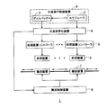
- FIG. 1 is a block diagram showing a schematic configuration of a production efficiency improvement system according to a first embodiment of the present invention.
- the figure which shows an example of the conveyance path
- the block diagram which showed an example of the structure of the processing apparatus.
- the block diagram which shows an example of the internal structure of the production efficiency improvement apparatus 4 which concerns on 1st Embodiment.
- the flowchart which shows an example of the processing operation of the production efficiency improvement apparatus 4.
- the block diagram which shows an example of the internal structure of the production efficiency improvement apparatus 4a which concerns on 2nd Embodiment.
- the block diagram which shows an example of an internal structure of the conveyance control apparatus 8 which concerns on 2nd Embodiment.
- FIG. 1 The sequence diagram which shows an example of processing operation of the production efficiency improvement apparatus 4a and the conveyance control apparatus 8.
- FIG. The figure which shows the example of a waiting
- the block diagram which shows the internal structure of the production efficiency improvement apparatus 4b which concerns on 3rd Embodiment.
- FIG. 1 is a block diagram showing a schematic configuration of a production efficiency improvement system according to the first embodiment of the present invention.
- 1 includes a scheduler 2, a dispatcher 3, a production efficiency device 4, a plurality of processing devices 5, a plurality of processing device controllers 6, a plurality of transport devices 7, and a transport control device. 8 and.
- the scheduler 2 creates a production plan for an object to be processed (for example, a semiconductor device) in a production factory (for example, a semiconductor manufacturing factory). This production plan is sequentially updated based on the production progress plan.
- the dispatcher 3 gives an operation instruction to the plurality of processing devices 5 that process the object to be processed based on the production plan created by the scheduler 2.
- the scheduler 2 and the dispatcher 3 together constitute a production execution control device (MES: Manufacturing Execute System) 9 and can actually be realized by, for example, one or a plurality of computers.
- MES Manufacturing Execute System
- the production efficiency improving device 4 controls the plurality of processing devices 5 based on the processing results of the scheduler 2 and the dispatcher 3. As will be described later, the production efficiency device 4 of the present embodiment has a device location map (not shown) indicating the position information of each processing device 5.
- the plurality of processing apparatuses 5 include, for example, a plasma CVD apparatus, a plasma etching apparatus, a sputtering apparatus, and a PVD apparatus that process an object to be processed such as a glass substrate for manufacturing an organic EL device or a silicon wafer for manufacturing a semiconductor device or the like.
- a plasma CVD apparatus a plasma etching apparatus
- a sputtering apparatus a PVD apparatus that process an object to be processed such as a glass substrate for manufacturing an organic EL device or a silicon wafer for manufacturing a semiconductor device or the like.
- the specific processing content is not questioned.
- the plurality of processing devices 5 may be classified into a plurality of groups that perform two or more processing devices 5 that perform the same processing as one group and perform different processing. Or when performing one process process continuously with the some processing apparatus 5, you may provide several groups which perform the same process process by making these processing apparatuses 5 into one group.
- a processing device controller 6 is provided in association with each of the plurality of processing devices 5. Upon receiving an instruction from the production efficiency improving device 4, these processing device controllers 6 control the operation of the corresponding processing device 5 and detect signals from various sensors (not shown) connected to the processing device 5.
- the type of the sensor is not particularly limited. For example, the temperature, humidity, gas flow rate, and degree of vacuum in the chamber in the processing apparatus 5 are measured.
- the transport device 7 is, for example, a transport shuttle that travels on a track installed on a ceiling or a floor, an automatic guided vehicle that travels on a predetermined route, and transports a transport container (carrier).
- the transfer device 7 moves between the plurality of processing devices 5 and the stocker storing the carrier based on an instruction given from the transfer control device 8 and transfers the object to be processed accommodated in the carrier. .
- the transport control device 8 constitutes a so-called MCS (Material Control System), and controls the operation of the transport device 7 based on the transport plan created by the scheduler 2.
- MCS Machine Control System
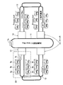
- FIG. 2 is a diagram illustrating an example of a conveyance path of the conveyance device 7.
- FIG. 2 shows a conveyance path in one process of the object to be processed.
- an inter-process (Inter-Bay) transport path 11 for transporting between processes is provided at the center, and an intra-process (Intra-Bay) transport path 12 is provided on both sides thereof. Yes.
- the left and right in-process conveyance paths 12 are substantially U-shaped, and the inter-process conveyance paths 11 are connected to the entrances at both ends.
- a stocker 13 for temporarily storing an object to be processed such as a wafer is provided at the entrance / exit of both ends of the in-process transfer path 12.
- the object to be processed conveyed from the inter-process conveyance path 11 is temporarily stored in the stocker 13 and then taken out at a desired timing and conveyed on the intra-process conveyance path 12.
- the stocker 13 is provided to absorb the difference between the processing completion timing in each processing apparatus 5 and the conveyance timing in the previous process or the next process.
- the in-process conveyance path 12 is, for example, a U-shaped rail installed on the ceiling or floor, and a conveyance device 7 (OHT: Overhead Hoist Transfer) having a hoist mechanism that moves up and down on the rail by belt driving travels. .
- OHT Overhead Hoist Transfer
- the transport device 7 is lowered by the hoist mechanism to mount the processing object on the processing device 5.
- the plurality of processing apparatuses 5 are arranged on both sides of the in-process conveyance path 12. As described above, the processing devices 5 that perform the same processing may be arranged close to each other as one group, and when one process process is shared by a plurality of processing devices 5, a plurality of processing devices 5 are arranged in the processing order. The processing devices 5 may be arranged side by side.
- the processing apparatuses 5 provided along one in-process conveyance path 12 constitute one group 20.
- the devices 5a to 5f constitute one group 20.
- a stocker 13 is provided corresponding to each of the groups 20.
- FIG. 2 there are two types of transfer devices 7. That is, the inter-process transport apparatus 7 a that moves on the inter-process transport path 11 and the intra-process transport apparatus 7 b that moves on the intra-process transport path 12.
- the transport apparatus 7a temporarily stores the object to be processed in the stocker 13 corresponding to the group 20 including the processing apparatus 5 that processes the object.
- the transport device 7 b transports the target object stored in the stocker 13 to the processing device 5. In the present embodiment, the energy of the transfer device 7b is reduced.
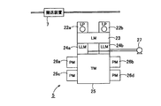
- FIG. 3 is a block diagram showing an example of the configuration of the processing device 5.
- the processing apparatus 5 is, for example, a multi-chamber type substrate processing system.
- the processing apparatus 5 includes a load module (LM: Load) provided with first and second load ports (LP: Load Ports) 22a and 22b on which carriers are placed in order to deliver a carrier that accommodates the workpiece W. Module) 23.
- a transfer module (TM: Transfer25 Module) 25 is connected to the load module 23 via load lock modules (LLM: Load Module) 241, 24b.
- LLM load lock modules
- a vacuum robot (not shown) included in the transfer module 25 conveys the workpiece W loaded through the load lock modules 241 and 24b to the process modules (PM: Process Module) 26a to 26d.
- PM Process Module
- the process modules 26a to 26d perform predetermined processing on the workpiece W based on the recipe.
- the processed object W is collected in a carrier placed on the first load port 22a or the second load port 22b along a path opposite to the carry-in, and is carried out in units of carriers.
- the process modules 26a to 26d and the transfer module 25 are always kept in a vacuum state, and the load lock modules 241 and 24b and the transfer module 25 are gate valves (not shown). ).
- the gate valve is opened in a state where the load lock modules 241 and 24b are evacuated, and the workpiece W is transported between the process modules 26a to 26d and the load lock modules 241 and 24b.
- a vacuum pump evacuates the load lock modules 241 and 24b.
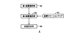
- FIG. 4 is a block diagram showing an example of the internal configuration of the production efficiency improvement device 4 according to the first embodiment.
- the production efficiency improving apparatus 4 in FIG. 4 includes an apparatus location map 41, a first apparatus selecting unit 42, a second apparatus selecting unit 43, and an apparatus answering unit 44.
- the processing operations of the first device selection unit 42, the second device selection unit 43, and the device response unit 44 may be performed by hardware or software. If the production efficiency improvement device 4 is configured by a computer, a program (software) for performing processing operations of each part of the production efficiency improvement device 4 is executed by the computer, so that all or part of the processing of the production efficiency improvement device 4 is performed by software. Can be realized.
- the device location map 41 indicates position information regarding each of the plurality of processing devices 5, and holds, for example, the position of each processing device 5 as coordinates.
- the transfer distance from the stocker 13 to each processing apparatus is the processing apparatuses 5 a, 5 b, 5 c when the object to be processed is transferred counterclockwise with reference to the stocker 13.
- 5d, 5e, and 5f and when the workpiece is conveyed clockwise with reference to the stocker 13, the processing devices 5f, 5e, 5d, 5c, 5b, and 5a are short in that order.
- the first device selection unit 42 When the first device selection unit 42 receives an inquiry from the scheduler 2 to the dispatcher 3 about the processing device 5 that sets an arbitrary product lot, the first device selection unit 42, based on the object to be processed and the product produced using the object to be processed, Among the plurality of processing devices 5 in the group 20, one or a plurality of devices 5 capable of processing the object to be processed are selected. For example, the processing device generated by the scheduler 2 is used to exclude the processing device 5 that is in use or maintenance, and the first device is considered in consideration of the processing required for the product to be produced and the required accuracy. The selection unit 42 selects the processing device 5.
- the second device selection unit 43 selects one of the processing devices 5 selected by the first device selection unit 42 in consideration of the device location map 41. More specifically, the second device selection unit 43 is, for example, a stocker among the processing devices 5 selected by the first device selection unit 42 so that the energy for transporting the object to be processed to the processing device 5 is reduced. The processing device 5 with the shortest transport distance from 13 is selected.
- the device reply unit 44 replies to the scheduler 2 to the dispatcher 3 with the processing device 5 selected by the second device selection unit 43 as a candidate for the processing device 5 that processes the object to be processed.
- one of the features of the present embodiment is that a candidate for the processing device 5 is selected in consideration of the device location map 41. If the apparatus location map 41 is not taken into consideration, there is a possibility that a distant processing apparatus 5 may be selected even when the processing apparatus 5 close to the stocker 13 can be used. In this case, the transport distance from the stocker 13 to the processing device 5 becomes long, and energy is wasted. On the other hand, in this embodiment, since the processing apparatus 5 close to the stocker 13 is selected, energy consumption can be reduced.
- FIG. 5 is a flowchart showing an example of the processing operation of the production efficiency system.
- the scheduler 2 to the dispatcher 3 transmit an inquiry of the processing device 5 for setting an arbitrary product lot (step S11).
- the first device selection unit 42 of the production efficiency improvement device 4 selects one or a plurality of processing devices 5 capable of processing the object to be processed (step S22).
- the second device selection unit 43 selects the processing device 5 having the shortest transport distance from the stocker 13 among the processing devices 5 selected by the first device selection unit 42 (step S23).
- the device answering unit 44 replies to the dispatcher 3 with the processing device 5 selected by the second device selection unit 43 as a candidate for the processing device 5 that processes the object to be processed (step S24).
- the scheduler 2 or the dispatcher 3 When the scheduler 2 or the dispatcher 3 receives the candidate for the processing device 5 (step S12), the scheduler 2 to the dispatcher 3 finally determines the candidate for the processing device 5 that has been answered (step S13). Then, the scheduler 2 to the dispatcher 3 instruct the transfer control device 8 to transfer the target object stored in the stocker 13 to the finally determined processing device 5 (step S14).
- the transport control device 8 inquires the production efficiency improving device 4 about the time when the workpiece can be transported to the finally determined processing device 5 (step S32). In response to this inquiry, the production efficiency improving device 4 replies to the transport control device 8 with a time when the workpiece can be transported to the processing device 5 (steps S25 and S26).
- the transport control device 8 receives a transportable time (step S33)
- a transport plan to the processing device 5 is created using this time as a transport scheduled time (step S34).
- the transfer control device 8 determines an optimal transfer route for transferring the object to be processed from the stocker 13 to the processing device 5 (step S35), and the transfer control device 8 determines the transfer device 7b. By controlling, the object to be processed stored in the stocker 13 is transported to the processing device 5 through the determined transport path.
- the processing device 5 that performs processing is selected in consideration of the arrangement of the processing devices 5, the transport distance of the transport device 7b can be shortened, and as a result, energy consumption can be reduced.
- the transport device 7b is efficiently moved to reduce energy consumption.
- a schematic configuration of a production efficiency improvement system 1 according to the second embodiment of the present invention is represented by a block diagram similar to FIG.
- FIG. 6 is a block diagram showing an example of the internal configuration of the production efficiency improving device 4a according to the second embodiment.
- the production efficiency improving apparatus 4a in the figure includes an apparatus state acquisition unit 45 and a conveyance instruction transmission unit 46.
- the apparatus state acquisition unit 45 acquires the state of each processing apparatus 5, more specifically, whether or not the processing apparatus 5 can mount the object to be processed from the processing apparatus controller 6.
- the conveyance instruction transmission unit 46 sends a conveyance instruction to the conveyance control device 8 and moves the conveyance device 7b to the processing device 5 in two stages. First, the conveyance instruction transmission unit 46 instructs to move the conveyance device 7 b from the stocker 13 to a standby position near the processing device 5. Thereafter, when the apparatus state acquisition unit 45 acquires that the processing apparatus 5 to which the object to be processed is carried is ready to mount the object to be processed, the conveyance instruction transmission unit 46 processes the conveyance apparatus 7b from the standby position. Instruct to move to the device 5.
- FIG. 7 is a block diagram showing an example of the internal configuration of the transport control device 8 according to the second embodiment.
- the conveyance control device 8 in the figure includes a conveyance instruction receiving unit 81 and a control unit 82.
- the conveyance instruction receiving unit 81 receives a conveyance instruction from the production efficiency improving device 4a.
- the controller 82 moves the transport device 7b based on the transport instruction.
- the processing operation of each part of the production efficiency improvement device 4a in FIG. 6 and the transfer control device 8 in FIG. 7 may also be performed by hardware or software.
- FIG. 8 is a sequence diagram showing an example of processing operations of the production efficiency improving device 4a and the conveyance control device 8.
- the processing apparatus 5 for processing the object to be processed has already been determined.
- the method for determining the processing device 5 is not particularly limited, and may be determined based on the device location map 41 as described in the first embodiment, or may be determined without considering the position of each processing device 5. May be.
- the transfer plan and the optimal transfer route have already been determined by the transfer control device 8.
- the scheduler 2 or the dispatcher 3 gives an instruction for conveyance to the conveyance control device 8 via the production efficiency improving device 4a.
- the transport instruction transmission unit 46 of the production efficiency improving device 4a moves the transport device 7b from the stocker 13 based on the processing plan of the plurality of processing devices 5. Then, a conveyance instruction for moving to a standby position in the vicinity of the processing apparatus 5 that performs the process is transmitted to the conveyance control apparatus 8 (step S41).
- the control unit 82 moves the transport device 7b from the stocker 13 to the standby position on the determined transport path based on the transport instruction.
- the workpiece is moved to the standby position (step S52).
- the control part 82 stops the energy supply to the conveying apparatus 7b in a stand-by position, and stops a movement once. Thereby, the conveying apparatus 7b will be in a state with low energy consumption.
- the reason why the object to be processed is not immediately carried into the processing apparatus 5 is that the processing apparatus 5 is performing a process on another object to be processed or is in a sleep state, and is necessarily in a state where the object to be processed can be mounted. Because there is no limit. Before the processing apparatus 5 can mount the object to be processed, the object to be processed is transported to a standby position in the vicinity thereof in advance, so that the processing efficiency can be improved.
- the standby position is provided at least at a position where the transport distance from the standby position to the processing device 5 is shorter than the transport distance from the stocker 13 to the processing device 5.
- the standby position may be provided on the in-process transfer path 11 of FIG. 2, but a standby path for temporarily retracting the transfer apparatus 7b may be provided.
- the standby path is provided by branching from the intra-process transport path 11, and may be, for example, a path 12a branched from the intra-process transport path 11 in a T shape as shown in FIG. As shown in b), it may be a bypass path 12b of the in-process transport path 11. By providing such a standby path, the transfer device 7b can be put on standby without hindering the movement of the other transfer device 7b.
- a conveyance instruction The transmission unit 46 transmits a conveyance instruction for moving the conveyance device 7b from the standby position to the processing device 5 to the conveyance control device 8 (step S43).
- step S53 When the conveyance instruction receiving unit 81 of the conveyance control device 8 receives this conveyance instruction (step S53), the control unit 82 supplies energy to the conveyance device 7b based on the conveyance instruction, and the conveyance device from the standby position to the processing device 5 is supplied. 7b is moved. Thereby, the to-be-processed object is conveyed to the processing apparatus 5, and is mounted in the processing apparatus 5 (step S54).
- the transfer control device 8 cannot receive a carry-in instruction from the production efficiency improving device 4a to the processing device 5, the transfer control device 8 does not know when the transfer device 7b may be moved to the processing device 5. . For this reason, the transfer device 7b has to circulate on the in-process transfer path 11 until the processing device 5 can be mounted, which wastes energy.
- the conveyance control device 8 cooperates with the production efficiency improving device 4a. Therefore, it can be stopped at the standby position until it can be mounted on the processing device 5, and energy consumption can be reduced compared to the case where the transport device 7b goes around. Further, since the standby position is provided in the vicinity of the processing apparatus 5, when the mountable state is reached, the object to be processed can be quickly conveyed to the processing apparatus 5 and the processing efficiency is improved.
- the object to be processed is conveyed to the vicinity of the processing apparatus 5 to temporarily stop the conveying apparatus 7b, and then the object to be processed is mounted when the processing apparatus 5 is mountable. It is carried into the processing device 5. Therefore, the transfer device 7b can be moved efficiently and energy consumption can be reduced. Further, hardware such as a temporary storage such as a buffer provided in the vicinity of the apparatus can be minimized.
- Schematic configuration of the production efficiency improvement system 1 according to the third embodiment of the present invention is represented by a block diagram similar to FIG. In the present embodiment, it is assumed that the maximum energy consumption consumed in the production efficiency improvement system 1 is determined in advance by a contract with an electric power company, etc. The device 7 is operated.
- the production efficiency improvement system 1 is premised on processing the object to be processed for each lot.
- a plurality of objects to be processed are processed by one or a plurality of processing apparatuses 5.
- the plurality of processing devices 5 are classified into a plurality of groups, with two or more processing devices 5 performing the same processing as a group.
- a plurality of objects in the same lot can be processed using a plurality of processing devices 5 belonging to the group.
- the same object to be processed may be processed, or different objects to be processed may be processed. Further, the number of objects to be processed in each lot may be the same or different. Information on how many types of objects to be processed in each lot is included in the processing plan of the processing device 5 created by the scheduler 2.
- the processing device controller (consumption energy management unit) 6 connected to each processing device 5 detects the energy consumption amount of the corresponding processing device 5 for each lot.
- the energy consumption amount of each processing device 5 detected by each processing device controller 6 is sent to the production efficiency improvement device 4 for each lot and totalized.
- the production efficiency improving device 4 determines in advance the energy consumed by the entire plurality of processing devices based on the energy consumption of each processing device managed by each processing device controller 6 and the processing results of the scheduler 2 and the dispatcher 3 in advance. Whether or not to process the object to be processed in each of the plurality of processing devices is determined for each lot so that the specified maximum energy consumption is not exceeded, and is consumed by the whole of the plurality of processing devices during the processing of each lot.
- the processing timing of each processing apparatus operating in each lot is individually adjusted so that the energy consumption does not exceed the maximum energy consumption. That is, the production efficiency improving device 4 manages the lot information, the type of processing device to be processed in each lot, and the timing for operating each processing device in each lot.
- FIG. 10 is a block diagram showing an internal configuration of the production efficiency improving device 4b according to the third embodiment.
- the production efficiency improvement device 4b of FIG. 10 includes an energy consumption totaling unit 61 that totalizes the energy consumption supplied from each processing device controller 6, a table creation unit 62 that tabulates the total energy consumption for each lot, A processing device determination unit 63 that determines a processing device 5 that is to process the next lot, and a transport timing determination unit 64 that determines the timing of transporting the object to be processed to each processing device 5 that is determined to be processed. .
- the processing device determination unit 63 grasps the type and number of objects to be processed in the next lot, and refers to the table creation unit 62 to determine in advance. In addition, the maximum number of processing devices 5 that can be operated within a range that does not exceed the maximum energy consumption amount is obtained, and the next lot can be reliably processed within a given time. In addition, the processing device determination unit 43 individually adjusts the processing timing of each processing device operating in each lot so that the energy consumption consumed by the entire plurality of processing devices does not exceed the maximum energy consumption during the processing of each lot. .
- Processing instructions are given to the processing devices 5 determined by the processing device determination unit 63 via the processing device controller 6 at a predetermined timing.
- the production efficiency improving device 4b instructs the transfer control device 8 to transfer the workpiece to each processing device 5 according to the transfer timing determined by the transfer timing determination unit 64.
- the total energy consumed by the plurality of processing devices 5 is controlled so as not to exceed the predetermined maximum energy consumption.
- the energy consumed when transported by the transport device 7 is also described. In consideration, the maximum energy consumption may not be controlled.
- the production efficiency improving device 4 determines, for each lot, the processing device 5 that processes the object to be processed, and also determines the timing at which the object to be processed is transported to each determined processing device 5, and each determined processing device The total amount of energy consumed in step 5 and the amount of consumed energy required to transport the object to be processed to each processing apparatus 5 are prevented from exceeding the maximum amount of energy consumed.
- the number of processing apparatuses 5 that process each object to be processed belonging to the lot is increased to the maximum, and the objects to be processed are connected to each processing apparatus 5 through the shortest path. So that the transfer timing of the transfer device 7 is scheduled. Thereby, it is possible to transport the objects to be processed at the shortest distance to as many processing apparatuses 5 as possible, and to perform processing of a plurality of objects to be processed at these processing apparatuses 5 almost simultaneously, while suppressing the total energy consumption, The production efficiency can be maximized.
- scheduling may be performed so as not to exceed the maximum energy consumption amount in consideration of the energy consumption amounts of devices other than the processing device 5 and the transfer device 7 included in the production efficiency improvement system 1 of FIG.
- the processing device determination unit 63 may determine the processing device 5 that processes the object to be processed in consideration of the arrangement of the processing devices 5 with reference to the device location map 41. Further, this embodiment may be combined with the above-described second embodiment. That is, the production efficiency improving apparatus 4b of FIG. 10 is further provided with the apparatus state acquisition unit 45 and the conveyance instruction transmission unit 46 of FIG. When transporting, the object to be processed may be temporarily stopped at the standby position until the processing apparatus 5 is ready to mount the object to be processed.
- the processing schedule of the processing device 5 is created for each lot so that the predetermined maximum energy consumption is not exceeded. Can be done efficiently.
- the processing device 5 and the transfer device 7 are scheduled for each lot so that the energy consumption of the entire production efficiency system 1 does not exceed the maximum energy consumption. It is also possible.
- At least a part of the production efficiency improvement system 1 described in the above-described embodiment may be configured by hardware or software.
- a program for realizing at least a part of the functions of the production efficiency improvement system 1 may be stored in a recording medium such as a flexible disk or a CD-ROM, and read and executed by a computer.
- the recording medium is not limited to a removable medium such as a magnetic disk or an optical disk, but may be a fixed recording medium such as a hard disk device or a memory.
- a program that realizes at least a part of the functions of the production efficiency improving system 1 may be distributed via a communication line (including wireless communication) such as the Internet. Further, the program may be distributed in a state where the program is encrypted, modulated or compressed, and stored in a recording medium via a wired line such as the Internet or a wireless line.
- a communication line including wireless communication
- the program may be distributed in a state where the program is encrypted, modulated or compressed, and stored in a recording medium via a wired line such as the Internet or a wireless line.
Landscapes
- Engineering & Computer Science (AREA)
- General Engineering & Computer Science (AREA)
- Manufacturing & Machinery (AREA)
- Quality & Reliability (AREA)
- Physics & Mathematics (AREA)
- General Physics & Mathematics (AREA)
- Automation & Control Theory (AREA)
- Container, Conveyance, Adherence, Positioning, Of Wafer (AREA)
- General Factory Administration (AREA)
Priority Applications (2)
| Application Number | Priority Date | Filing Date | Title |
|---|---|---|---|
| KR1020147016031A KR101953423B1 (ko) | 2011-12-13 | 2012-11-08 | 생산 효율화 시스템, 생산 효율화 장치 및 생산 효율화 방법 |
| US14/303,059 US10012980B2 (en) | 2011-12-13 | 2014-06-12 | Modifying operational efficiency by repositioning process apparatus |
Applications Claiming Priority (2)
| Application Number | Priority Date | Filing Date | Title |
|---|---|---|---|
| JP2011-272476 | 2011-12-13 | ||
| JP2011272476A JP6017134B2 (ja) | 2011-12-13 | 2011-12-13 | 生産効率化システム、生産効率化装置および生産効率化方法 |
Related Child Applications (1)
| Application Number | Title | Priority Date | Filing Date |
|---|---|---|---|
| US14/303,059 Continuation US10012980B2 (en) | 2011-12-13 | 2014-06-12 | Modifying operational efficiency by repositioning process apparatus |
Publications (1)
| Publication Number | Publication Date |
|---|---|
| WO2013088865A1 true WO2013088865A1 (ja) | 2013-06-20 |
Family
ID=48612320
Family Applications (1)
| Application Number | Title | Priority Date | Filing Date |
|---|---|---|---|
| PCT/JP2012/078923 Ceased WO2013088865A1 (ja) | 2011-12-13 | 2012-11-08 | 生産効率化システム、生産効率化装置および生産効率化方法 |
Country Status (5)
| Country | Link |
|---|---|
| US (1) | US10012980B2 (enExample) |
| JP (1) | JP6017134B2 (enExample) |
| KR (1) | KR101953423B1 (enExample) |
| TW (1) | TWI557655B (enExample) |
| WO (1) | WO2013088865A1 (enExample) |
Cited By (1)
| Publication number | Priority date | Publication date | Assignee | Title |
|---|---|---|---|---|
| WO2018153153A1 (zh) * | 2017-02-23 | 2018-08-30 | 惠科股份有限公司 | 一种搬运管理的方法及系统 |
Families Citing this family (9)
| Publication number | Priority date | Publication date | Assignee | Title |
|---|---|---|---|---|
| JP6172022B2 (ja) * | 2014-03-28 | 2017-08-02 | 株式会社デンソー | 搬送システム |
| JP6330596B2 (ja) * | 2014-09-16 | 2018-05-30 | 株式会社デンソー | 搬送システム |
| DE102015211941A1 (de) * | 2015-06-26 | 2016-12-29 | Zf Friedrichshafen Ag | Verfahren und Vorrichtung zur Reduzierung eines Energiebedarfs einer Werkzeugmaschine und Werkzeugmaschinensystem |
| NL2017837A (en) * | 2015-11-25 | 2017-06-02 | Asml Netherlands Bv | A Measurement Substrate and a Measurement Method |
| WO2017098813A1 (ja) * | 2015-12-09 | 2017-06-15 | 村田機械株式会社 | 搬送システム及び搬送方法 |
| JP6605951B2 (ja) * | 2015-12-25 | 2019-11-13 | 株式会社東芝 | シミュレーション装置及びシミュレーション方法 |
| CN107024867B (zh) * | 2017-06-01 | 2019-10-25 | 合肥工业大学 | 一种考虑前视距离的相容工件族的优化控制方法 |
| JP6792098B1 (ja) * | 2019-02-07 | 2020-11-25 | 株式会社日立ハイテク | 真空処理装置の運転方法 |
| KR102876296B1 (ko) * | 2021-10-07 | 2025-10-23 | 주식회사 엘지에너지솔루션 | 자동 안내 차량을 이용한 자동 운반 제어 방법 및 자동 운반 시스템 |
Citations (4)
| Publication number | Priority date | Publication date | Assignee | Title |
|---|---|---|---|---|
| JP2000200822A (ja) * | 1998-10-30 | 2000-07-18 | Tokyo Electron Ltd | 処理システム |
| JP2002359272A (ja) * | 2001-05-31 | 2002-12-13 | Hirata Corp | 処理システム |
| JP2007273888A (ja) * | 2006-03-31 | 2007-10-18 | Tokyo Electron Ltd | 基板処理装置の制御装置,制御方法および制御プログラムを記憶した記録媒体 |
| JP2010238783A (ja) * | 2009-03-30 | 2010-10-21 | Dainippon Screen Mfg Co Ltd | 基板処理装置および基板搬送方法 |
Family Cites Families (45)
| Publication number | Priority date | Publication date | Assignee | Title |
|---|---|---|---|---|
| US4977361A (en) * | 1978-06-26 | 1990-12-11 | Eaton Corporation | X-Y addressable workpiece positioner and mask aligner using same |
| US4687980A (en) * | 1980-10-20 | 1987-08-18 | Eaton Corporation | X-Y addressable workpiece positioner and mask aligner using same |
| US4425537A (en) * | 1978-06-26 | 1984-01-10 | Optimetrix Corporation | X-Y Addressable workpiece positioner and mask aligner using same |
| US4442388A (en) * | 1980-04-02 | 1984-04-10 | Optimetrix Corporation | X-Y Addressable workpiece positioner having an improved X-Y address indicia sensor |
| US5399531A (en) | 1990-12-17 | 1995-03-21 | United Micrpelectronics Corporation | Single semiconductor wafer transfer method and plural processing station manufacturing system |
| FR2676018B1 (fr) * | 1991-05-02 | 1997-06-06 | Prodel Jacques | Installation pour la circulation de palettes motorisees porte-pieces. |
| DE4418206C2 (de) * | 1994-05-25 | 1999-01-14 | Siemens Ag | CMOS-kompatibler Bipolartransistor und Herstellungsverfahren desselben |
| US6991012B2 (en) * | 1996-03-21 | 2006-01-31 | Coe Newnes/Mcgehee Inc. | Apparatus for sawing a workpiece |
| USRE39579E1 (en) * | 1997-04-04 | 2007-04-17 | Renesas Technology Corp. | Semiconductor integrated circuit device comprising RAM with command decode system and logic circuit integrated into a single chip and testing method of the RAM with command decode system |
| US6269279B1 (en) * | 1997-06-20 | 2001-07-31 | Tokyo Electron Limited | Control system |
| JP2000099557A (ja) * | 1998-09-25 | 2000-04-07 | Hitachi Ltd | 半導体集積回路装置、及びその製造方法、及び記憶媒体 |
| TW425598B (en) * | 1998-10-30 | 2001-03-11 | Tokyo Electron Ltd | Processing system |
| JP3487774B2 (ja) | 1998-11-19 | 2004-01-19 | 沖電気工業株式会社 | 半導体装置製造工程の搬送方法 |
| JP4666723B2 (ja) * | 1999-07-06 | 2011-04-06 | 株式会社半導体エネルギー研究所 | 半導体装置の作製方法 |
| US6952020B1 (en) * | 1999-07-06 | 2005-10-04 | Semiconductor Energy Laboratory Co., Ltd. | Semiconductor device and manufacturing method thereof |
| EP1258915A1 (en) * | 2001-05-17 | 2002-11-20 | Infineon Technologies SC300 GmbH & Co. KG | Method of detecting defects on a semiconductor device in a processing tool and an arrangement therefore |
| US6944842B1 (en) * | 2001-06-27 | 2005-09-13 | Xilinx, Inc. | Method for making large-scale ASIC using pre-engineered long distance routing structure |
| US6601227B1 (en) * | 2001-06-27 | 2003-07-29 | Xilinx, Inc. | Method for making large-scale ASIC using pre-engineered long distance routing structure |
| WO2003010614A1 (en) * | 2001-07-24 | 2003-02-06 | Honda Giken Kogyo Kabushiki Kaisha | Work transfer method and system |
| JP4073186B2 (ja) | 2001-09-20 | 2008-04-09 | 大日本スクリーン製造株式会社 | 基板処理装置のスケジュール作成方法及びそのプログラム |
| US6615093B1 (en) * | 2002-01-04 | 2003-09-02 | Taiwan Semiconductor Manufacturing Company | Adaptive control algorithm for improving AMHS push lot accuracy |
| US8621786B2 (en) * | 2003-02-13 | 2014-01-07 | Wei Chak Joseph Lam | Efficient layout and design of production facility |
| US7269925B2 (en) * | 2002-06-14 | 2007-09-18 | Wei Chak Joseph Lam | Layout of production facility |
| CN1288315C (zh) * | 2002-06-14 | 2006-12-06 | 约瑟夫·林惠泽 | 生产企业布局和设计 |
| US6871115B2 (en) * | 2002-10-11 | 2005-03-22 | Taiwan Semiconductor Manufacturing Co., Ltd | Method and apparatus for monitoring the operation of a wafer handling robot |
| JP3999649B2 (ja) | 2002-12-19 | 2007-10-31 | 大日本スクリーン製造株式会社 | 基板処理装置とその動作方法、およびプログラム |
| JP4143828B2 (ja) | 2003-03-14 | 2008-09-03 | 村田機械株式会社 | 搬送台車システム |
| JP4449319B2 (ja) * | 2003-03-25 | 2010-04-14 | 株式会社デンソー | 製造管理方法 |
| US7861228B2 (en) * | 2003-12-03 | 2010-12-28 | Hewlett-Packard Development Company, L.P. | Variable delay instruction for implementation of temporal redundancy |
| TW200525601A (en) * | 2004-01-07 | 2005-08-01 | Trecenti Technologies Inc | Semiconductor manufacturing system, work manufacturing system, and conveyance system |
| US7512455B2 (en) * | 2004-03-29 | 2009-03-31 | Palo Alto Research Center Incorporated | Method for self-synchronization of modular production systems |
| US7203563B2 (en) * | 2004-04-08 | 2007-04-10 | Taiwan Semiconductor Manufacturing Company, Ltd. | Automatic N2 purge system for 300 mm full automation fab |
| US7966714B2 (en) * | 2004-10-12 | 2011-06-28 | Precision Automation, Inc. | Multi-step systems for processing workpieces |
| KR101388345B1 (ko) * | 2005-09-09 | 2014-04-22 | 가부시키가이샤 니콘 | 노광 장치 및 노광 방법, 그리고 디바이스 제조 방법 |
| KR100714274B1 (ko) * | 2005-10-24 | 2007-05-02 | 삼성전자주식회사 | 반도체 제조설비의 관리시스템 |
| TW200719423A (en) * | 2005-11-04 | 2007-05-16 | Powerchip Semiconductor Corp | A method for material handling analysis |
| JP5091413B2 (ja) | 2006-03-08 | 2012-12-05 | 東京エレクトロン株式会社 | 基板処理装置および基板処理装置の制御方法 |
| JP2008124194A (ja) * | 2006-11-10 | 2008-05-29 | Canon Inc | 液浸露光方法および液浸露光装置 |
| KR20100033527A (ko) | 2007-07-11 | 2010-03-30 | 히다치 가세고교 가부시끼가이샤 | 회로 부재 접속용 접착제 |
| US8396826B2 (en) * | 2007-12-17 | 2013-03-12 | Landmark Graphics Corporation | Systems and methods for optimization of real time production operations |
| US8170861B2 (en) * | 2008-07-29 | 2012-05-01 | GM Global Technology Operations LLC | Method for distributed hybrid emulation of manufacturing systems |
| US8781882B1 (en) * | 2008-08-07 | 2014-07-15 | Accenture Global Services Limited | Automotive industry high performance capability assessment |
| JP5119506B2 (ja) * | 2009-05-20 | 2013-01-16 | 日本電気株式会社 | 半導体集積回路の設計装置、そのデータ処理方法、およびその制御プログラム |
| EP2264529A3 (en) * | 2009-06-16 | 2011-02-09 | ASML Netherlands B.V. | A lithographic apparatus, a method of controlling the apparatus and a method of manufacturing a device using a lithographic apparatus |
| WO2013077191A1 (ja) * | 2011-11-25 | 2013-05-30 | 東京エレクトロン株式会社 | 処理装置群コントローラ、生産処理システム、処理装置群制御方法、生産効率化システム、生産効率化装置および生産効率化方法 |
-
2011
- 2011-12-13 JP JP2011272476A patent/JP6017134B2/ja not_active Expired - Fee Related
-
2012
- 2012-11-08 KR KR1020147016031A patent/KR101953423B1/ko not_active Expired - Fee Related
- 2012-11-08 WO PCT/JP2012/078923 patent/WO2013088865A1/ja not_active Ceased
- 2012-12-12 TW TW101146792A patent/TWI557655B/zh not_active IP Right Cessation
-
2014
- 2014-06-12 US US14/303,059 patent/US10012980B2/en active Active
Patent Citations (4)
| Publication number | Priority date | Publication date | Assignee | Title |
|---|---|---|---|---|
| JP2000200822A (ja) * | 1998-10-30 | 2000-07-18 | Tokyo Electron Ltd | 処理システム |
| JP2002359272A (ja) * | 2001-05-31 | 2002-12-13 | Hirata Corp | 処理システム |
| JP2007273888A (ja) * | 2006-03-31 | 2007-10-18 | Tokyo Electron Ltd | 基板処理装置の制御装置,制御方法および制御プログラムを記憶した記録媒体 |
| JP2010238783A (ja) * | 2009-03-30 | 2010-10-21 | Dainippon Screen Mfg Co Ltd | 基板処理装置および基板搬送方法 |
Cited By (1)
| Publication number | Priority date | Publication date | Assignee | Title |
|---|---|---|---|---|
| WO2018153153A1 (zh) * | 2017-02-23 | 2018-08-30 | 惠科股份有限公司 | 一种搬运管理的方法及系统 |
Also Published As
| Publication number | Publication date |
|---|---|
| TW201346790A (zh) | 2013-11-16 |
| US10012980B2 (en) | 2018-07-03 |
| JP2013125788A (ja) | 2013-06-24 |
| TWI557655B (zh) | 2016-11-11 |
| KR20140102678A (ko) | 2014-08-22 |
| US20140297017A1 (en) | 2014-10-02 |
| JP6017134B2 (ja) | 2016-10-26 |
| KR101953423B1 (ko) | 2019-02-28 |
Similar Documents
| Publication | Publication Date | Title |
|---|---|---|
| JP6017134B2 (ja) | 生産効率化システム、生産効率化装置および生産効率化方法 | |
| KR101930981B1 (ko) | 처리 장치군 컨트롤러, 생산 처리 시스템, 처리 장치군 제어 방법, 생산 효율화 시스템, 생산 효율화 장치 및 생산 효율화 방법 | |
| US8204617B2 (en) | Methods and apparatus for enhanced operation of substrate carrier handlers | |
| US20130013103A1 (en) | Control apparatus, a substrate treating method, a substrate treating system, a method of operating a substrate treating system, a load port control apparatus, and a substrate treating system having the load port control apparatus | |
| JP5946617B2 (ja) | 基板処理システム | |
| KR101954475B1 (ko) | 생산 처리 시스템, 생산 처리의 제어 장치, 생산 처리의 제어 방법 및 생산 처리의 제어 프로그램 | |
| US7809466B2 (en) | Transportation system and transportation method | |
| US20100074717A1 (en) | Automatic transport system and control method thereof | |
| JP6294427B2 (ja) | 生産処理システムおよび生産効率化方法 | |
| KR101079487B1 (ko) | 기판 캐리어 핸들러의 향상된 동작을 위한 방법 및 장치 | |
| JP2013125839A (ja) | 生産効率化システム、生産効率化装置および生産効率化方法 | |
| JP6293845B2 (ja) | 生産効率化システム、生産効率化装置および生産効率化方法 | |
| JP2013115117A (ja) | 資源再利用装置、処理装置群コントローラ、資源再利用システム、資源再利用方法、及び資源再利用プログラム | |
| CN100511629C (zh) | 处理系统及其运作方法 | |
| JP5337543B2 (ja) | 搬送制御方法、制御装置及び搬送システム | |
| JP5076701B2 (ja) | 搬送システム、配車管理装置及び方法、並びにコンピュータプログラム | |
| US20240096674A1 (en) | Container relay unit and logistics transport system including the same | |
| JP2013114328A (ja) | 処理装置群コントローラ、生産処理システム、処理装置群制御方法、及びプログラム |
Legal Events
| Date | Code | Title | Description |
|---|---|---|---|
| 121 | Ep: the epo has been informed by wipo that ep was designated in this application |
Ref document number: 12858414 Country of ref document: EP Kind code of ref document: A1 |
|
| ENP | Entry into the national phase |
Ref document number: 20147016031 Country of ref document: KR Kind code of ref document: A |
|
| NENP | Non-entry into the national phase |
Ref country code: DE |
|
| 122 | Ep: pct application non-entry in european phase |
Ref document number: 12858414 Country of ref document: EP Kind code of ref document: A1 |