JP6017134B2 - 生産効率化システム、生産効率化装置および生産効率化方法 - Google Patents
生産効率化システム、生産効率化装置および生産効率化方法 Download PDFInfo
- Publication number
- JP6017134B2 JP6017134B2 JP2011272476A JP2011272476A JP6017134B2 JP 6017134 B2 JP6017134 B2 JP 6017134B2 JP 2011272476 A JP2011272476 A JP 2011272476A JP 2011272476 A JP2011272476 A JP 2011272476A JP 6017134 B2 JP6017134 B2 JP 6017134B2
- Authority
- JP
- Japan
- Prior art keywords
- processing
- processed
- production efficiency
- transfer
- transport
- Prior art date
- Legal status (The legal status is an assumption and is not a legal conclusion. Google has not performed a legal analysis and makes no representation as to the accuracy of the status listed.)
- Expired - Fee Related
Links
Images


Classifications
-
- G—PHYSICS
- G05—CONTROLLING; REGULATING
- G05B—CONTROL OR REGULATING SYSTEMS IN GENERAL; FUNCTIONAL ELEMENTS OF SUCH SYSTEMS; MONITORING OR TESTING ARRANGEMENTS FOR SUCH SYSTEMS OR ELEMENTS
- G05B19/00—Programme-control systems
- G05B19/02—Programme-control systems electric
- G05B19/418—Total factory control, i.e. centrally controlling a plurality of machines, e.g. direct or distributed numerical control [DNC], flexible manufacturing systems [FMS], integrated manufacturing systems [IMS], computer integrated manufacturing [CIM]
- G05B19/4189—Total factory control, i.e. centrally controlling a plurality of machines, e.g. direct or distributed numerical control [DNC], flexible manufacturing systems [FMS], integrated manufacturing systems [IMS], computer integrated manufacturing [CIM] characterised by the transport system
-
- G—PHYSICS
- G05—CONTROLLING; REGULATING
- G05B—CONTROL OR REGULATING SYSTEMS IN GENERAL; FUNCTIONAL ELEMENTS OF SUCH SYSTEMS; MONITORING OR TESTING ARRANGEMENTS FOR SUCH SYSTEMS OR ELEMENTS
- G05B2219/00—Program-control systems
- G05B2219/30—Nc systems
- G05B2219/31—From computer integrated manufacturing till monitoring
- G05B2219/31277—Dispatching rules, shortest travel time or bidding based to reduce empty travel
-
- G—PHYSICS
- G05—CONTROLLING; REGULATING
- G05B—CONTROL OR REGULATING SYSTEMS IN GENERAL; FUNCTIONAL ELEMENTS OF SUCH SYSTEMS; MONITORING OR TESTING ARRANGEMENTS FOR SUCH SYSTEMS OR ELEMENTS
- G05B2219/00—Program-control systems
- G05B2219/30—Nc systems
- G05B2219/32—Operator till task planning
- G05B2219/32271—Decision of job dispatching, select job to process next on each machine
-
- G—PHYSICS
- G05—CONTROLLING; REGULATING
- G05B—CONTROL OR REGULATING SYSTEMS IN GENERAL; FUNCTIONAL ELEMENTS OF SUCH SYSTEMS; MONITORING OR TESTING ARRANGEMENTS FOR SUCH SYSTEMS OR ELEMENTS
- G05B2219/00—Program-control systems
- G05B2219/30—Nc systems
- G05B2219/45—Nc applications
- G05B2219/45031—Manufacturing semiconductor wafers
-
- H—ELECTRICITY
- H01—ELECTRIC ELEMENTS
- H01L—SEMICONDUCTOR DEVICES NOT COVERED BY CLASS H10
- H01L21/00—Processes or apparatus adapted for the manufacture or treatment of semiconductor or solid state devices or of parts thereof
- H01L21/67—Apparatus specially adapted for handling semiconductor or electric solid state devices during manufacture or treatment thereof; Apparatus specially adapted for handling wafers during manufacture or treatment of semiconductor or electric solid state devices or components ; Apparatus not specifically provided for elsewhere
- H01L21/67005—Apparatus not specifically provided for elsewhere
- H01L21/67242—Apparatus for monitoring, sorting or marking
- H01L21/67276—Production flow monitoring, e.g. for increasing throughput
-
- H—ELECTRICITY
- H01—ELECTRIC ELEMENTS
- H01L—SEMICONDUCTOR DEVICES NOT COVERED BY CLASS H10
- H01L21/00—Processes or apparatus adapted for the manufacture or treatment of semiconductor or solid state devices or of parts thereof
- H01L21/67—Apparatus specially adapted for handling semiconductor or electric solid state devices during manufacture or treatment thereof; Apparatus specially adapted for handling wafers during manufacture or treatment of semiconductor or electric solid state devices or components ; Apparatus not specifically provided for elsewhere
- H01L21/677—Apparatus specially adapted for handling semiconductor or electric solid state devices during manufacture or treatment thereof; Apparatus specially adapted for handling wafers during manufacture or treatment of semiconductor or electric solid state devices or components ; Apparatus not specifically provided for elsewhere for conveying, e.g. between different workstations
- H01L21/67703—Apparatus specially adapted for handling semiconductor or electric solid state devices during manufacture or treatment thereof; Apparatus specially adapted for handling wafers during manufacture or treatment of semiconductor or electric solid state devices or components ; Apparatus not specifically provided for elsewhere for conveying, e.g. between different workstations between different workstations
- H01L21/67727—Apparatus specially adapted for handling semiconductor or electric solid state devices during manufacture or treatment thereof; Apparatus specially adapted for handling wafers during manufacture or treatment of semiconductor or electric solid state devices or components ; Apparatus not specifically provided for elsewhere for conveying, e.g. between different workstations between different workstations using a general scheme of a conveying path within a factory
-
- Y—GENERAL TAGGING OF NEW TECHNOLOGICAL DEVELOPMENTS; GENERAL TAGGING OF CROSS-SECTIONAL TECHNOLOGIES SPANNING OVER SEVERAL SECTIONS OF THE IPC; TECHNICAL SUBJECTS COVERED BY FORMER USPC CROSS-REFERENCE ART COLLECTIONS [XRACs] AND DIGESTS
- Y02—TECHNOLOGIES OR APPLICATIONS FOR MITIGATION OR ADAPTATION AGAINST CLIMATE CHANGE
- Y02P—CLIMATE CHANGE MITIGATION TECHNOLOGIES IN THE PRODUCTION OR PROCESSING OF GOODS
- Y02P80/00—Climate change mitigation technologies for sector-wide applications
- Y02P80/10—Efficient use of energy, e.g. using compressed air or pressurized fluid as energy carrier
-
- Y—GENERAL TAGGING OF NEW TECHNOLOGICAL DEVELOPMENTS; GENERAL TAGGING OF CROSS-SECTIONAL TECHNOLOGIES SPANNING OVER SEVERAL SECTIONS OF THE IPC; TECHNICAL SUBJECTS COVERED BY FORMER USPC CROSS-REFERENCE ART COLLECTIONS [XRACs] AND DIGESTS
- Y02—TECHNOLOGIES OR APPLICATIONS FOR MITIGATION OR ADAPTATION AGAINST CLIMATE CHANGE
- Y02P—CLIMATE CHANGE MITIGATION TECHNOLOGIES IN THE PRODUCTION OR PROCESSING OF GOODS
- Y02P90/00—Enabling technologies with a potential contribution to greenhouse gas [GHG] emissions mitigation
- Y02P90/02—Total factory control, e.g. smart factories, flexible manufacturing systems [FMS] or integrated manufacturing systems [IMS]
Description
所定位置から前記選択された処理装置へ、前記被処理体を搬送する搬送装置を移動させる搬送制御装置と、を備えることを特徴とする生産効率化システムが提供される。
前記搬送指示送信部からの搬送指示に応じて、前記所定位置から前記処理装置の近傍の待機位置へ、前記被処理体を搬送する搬送装置を移動させ、この待機位置で前記搬送装置を停止させ、その後、前記処理装置が前記被処理体をマウント可能な状態になったことを前記装置状態取得部が取得すると、前記待機位置から前記処理装置へ前記搬送装置を移動させる搬送制御装置と、を備えることを特徴とする生産効率化システムが提供される。
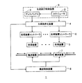
図1は本発明の第1の実施形態に係る生産効率化システムの概略構成を示すブロック図である。図1の生産効率化システム1は、スケジューラ2と、ディスパッチャ3と、生産効率化装置4と、複数の処理装置5と、複数の処理装置コントローラ6と、複数の搬送装置7と、搬送制御装置8とを備えている。
第2の実施形態は、搬送装置7bを効率的に移動させて、消費エネルギー低減を図るものである。本発明の第2の実施形態に係る生産効率化システム1の概略構成は、図1と同様のブロック図で表される。
第3の実施形態は、複数の処理装置5および搬送装置7での消費エネルギーの総量が最大消費エネルギー量を超えないように調整するものである。
また、本実施形態を、上述した第2の実施形態と組み合わせてもよい。すなわち、図10の生産効率化装置4bに、さらに、図6の装置状態取得部45および搬送指示送信部46を設け、搬送タイミング判定部64が判定した搬送経路に従って被処理体を処理装置5まで搬送する際に、処理装置5が被処理体をマウント可能な状態になるまで、被処理体を待機位置で一旦停止させるようにしてもよい。
2 スケジューラ
3 ディスパッチャ
4,4a,4b 生産効率化装置
5 処理装置
6 処理装置コントローラ
7,7a,7b 搬送装置
8 搬送制御装置
9 生産実行制御装置
11 工程間搬送路
12 工程内搬送路
13 ストッカ
41 装置ロケーションマップ
42 第1装置選択部
43 第2装置選択部
44 装置回答部
45 装置状態取得部
46 搬送指示送信部
61 エネルギー消費量集計部
62 テーブル作成部
63 処理装置判定部
64 搬送タイミング判定部
81 搬送指示受信部
82 制御部
Claims (4)
- 工程内搬送経路上に配置された複数の処理装置のそれぞれの位置を考慮して、被処理体を処理すべき処理装置を選択する生産効率化装置と、
所定位置から前記選択された処理装置へ、前記被処理体を搬送する搬送装置を移動させる搬送制御装置と、を備え、
前記生産効率化装置は、
前記複数の処理装置から前記被処理体を処理可能な2以上の処理装置を選択する第1装置選択部と、
前記第1装置選択部により選択された処理装置の中から、前記所定位置からの搬送距離が最も短い処理装置を選択する第2装置選択部と、を有することを特徴とする生産処理システム。 - 前記第1装置選択部は、前記被処理体を用いて生産される製品に応じて、前記被処理体を処理可能な処理装置を選択することを特徴とする請求項1に記載の生産処理システム。
- 前記生産効率化装置は、前記選択された処理装置の状態を取得する装置状態取得部を有し、
前記搬送制御装置は、
前記所定位置から前記選択された処理装置の近傍の待機位置へ前記搬送装置を移動させ、この待機位置で前記搬送装置を停止させ、
その後、前記選択された処理装置が前記被処理体を搬入できる状態になったことを前記装置状態取得部が取得すると、前記待機位置から前記選択された処理装置へ前記搬送装置を移動させることを特徴とする請求項1または2に記載の生産処理システム。 - 前記複数の処理装置のそれぞれに対して設けられ、対応する処理装置の消費エネルギーを管理する複数の消費エネルギー管理部を備え、
前記生産効率化装置は、前記消費エネルギー管理部で管理している処理装置の消費エネルギーと、前記搬送装置の消費エネルギーと、に基づいて、前記複数の処理装置全体および前記搬送装置で消費する消費エネルギーが予め定めた最大消費エネルギーを超えないように、前記被処理体を処理すべき処理装置を選択することを特徴とする請求項1乃至3のいずれかに記載の生産処理システム。
Priority Applications (5)
| Application Number | Priority Date | Filing Date | Title |
|---|---|---|---|
| JP2011272476A JP6017134B2 (ja) | 2011-12-13 | 2011-12-13 | 生産効率化システム、生産効率化装置および生産効率化方法 |
| KR1020147016031A KR101953423B1 (ko) | 2011-12-13 | 2012-11-08 | 생산 효율화 시스템, 생산 효율화 장치 및 생산 효율화 방법 |
| PCT/JP2012/078923 WO2013088865A1 (ja) | 2011-12-13 | 2012-11-08 | 生産効率化システム、生産効率化装置および生産効率化方法 |
| TW101146792A TWI557655B (zh) | 2011-12-13 | 2012-12-12 | Production efficiency system, production efficiency of the device and production efficiency of the method |
| US14/303,059 US10012980B2 (en) | 2011-12-13 | 2014-06-12 | Modifying operational efficiency by repositioning process apparatus |
Applications Claiming Priority (1)
| Application Number | Priority Date | Filing Date | Title |
|---|---|---|---|
| JP2011272476A JP6017134B2 (ja) | 2011-12-13 | 2011-12-13 | 生産効率化システム、生産効率化装置および生産効率化方法 |
Related Child Applications (1)
| Application Number | Title | Priority Date | Filing Date |
|---|---|---|---|
| JP2016194348A Division JP6294427B2 (ja) | 2016-09-30 | 2016-09-30 | 生産処理システムおよび生産効率化方法 |
Publications (3)
| Publication Number | Publication Date |
|---|---|
| JP2013125788A JP2013125788A (ja) | 2013-06-24 |
| JP2013125788A5 JP2013125788A5 (ja) | 2015-01-29 |
| JP6017134B2 true JP6017134B2 (ja) | 2016-10-26 |
Family
ID=48612320
Family Applications (1)
| Application Number | Title | Priority Date | Filing Date |
|---|---|---|---|
| JP2011272476A Expired - Fee Related JP6017134B2 (ja) | 2011-12-13 | 2011-12-13 | 生産効率化システム、生産効率化装置および生産効率化方法 |
Country Status (5)
| Country | Link |
|---|---|
| US (1) | US10012980B2 (ja) |
| JP (1) | JP6017134B2 (ja) |
| KR (1) | KR101953423B1 (ja) |
| TW (1) | TWI557655B (ja) |
| WO (1) | WO2013088865A1 (ja) |
Families Citing this family (9)
| Publication number | Priority date | Publication date | Assignee | Title |
|---|---|---|---|---|
| JP6172022B2 (ja) * | 2014-03-28 | 2017-08-02 | 株式会社デンソー | 搬送システム |
| JP6330596B2 (ja) * | 2014-09-16 | 2018-05-30 | 株式会社デンソー | 搬送システム |
| DE102015211941A1 (de) * | 2015-06-26 | 2016-12-29 | Zf Friedrichshafen Ag | Verfahren und Vorrichtung zur Reduzierung eines Energiebedarfs einer Werkzeugmaschine und Werkzeugmaschinensystem |
| NL2017837A (en) * | 2015-11-25 | 2017-06-02 | Asml Netherlands Bv | A Measurement Substrate and a Measurement Method |
| CN108352349B (zh) * | 2015-12-09 | 2022-07-22 | 村田机械株式会社 | 输送系统和输送方法 |
| JP6605951B2 (ja) * | 2015-12-25 | 2019-11-13 | 株式会社東芝 | シミュレーション装置及びシミュレーション方法 |
| CN106909129B (zh) * | 2017-02-23 | 2019-10-18 | 惠科股份有限公司 | 一种搬运管理的方法及系统 |
| CN107024867B (zh) * | 2017-06-01 | 2019-10-25 | 合肥工业大学 | 一种考虑前视距离的相容工件族的优化控制方法 |
| JP6792098B1 (ja) * | 2019-02-07 | 2020-11-25 | 株式会社日立ハイテク | 真空処理装置の運転方法 |
Family Cites Families (49)
| Publication number | Priority date | Publication date | Assignee | Title |
|---|---|---|---|---|
| US4687980A (en) * | 1980-10-20 | 1987-08-18 | Eaton Corporation | X-Y addressable workpiece positioner and mask aligner using same |
| US4425537A (en) * | 1978-06-26 | 1984-01-10 | Optimetrix Corporation | X-Y Addressable workpiece positioner and mask aligner using same |
| US4977361A (en) * | 1978-06-26 | 1990-12-11 | Eaton Corporation | X-Y addressable workpiece positioner and mask aligner using same |
| US4442388A (en) * | 1980-04-02 | 1984-04-10 | Optimetrix Corporation | X-Y Addressable workpiece positioner having an improved X-Y address indicia sensor |
| US5399531A (en) | 1990-12-17 | 1995-03-21 | United Micrpelectronics Corporation | Single semiconductor wafer transfer method and plural processing station manufacturing system |
| FR2676018B1 (fr) * | 1991-05-02 | 1997-06-06 | Prodel Jacques | Installation pour la circulation de palettes motorisees porte-pieces. |
| DE4418206C2 (de) * | 1994-05-25 | 1999-01-14 | Siemens Ag | CMOS-kompatibler Bipolartransistor und Herstellungsverfahren desselben |
| US6991012B2 (en) * | 1996-03-21 | 2006-01-31 | Coe Newnes/Mcgehee Inc. | Apparatus for sawing a workpiece |
| USRE39579E1 (en) * | 1997-04-04 | 2007-04-17 | Renesas Technology Corp. | Semiconductor integrated circuit device comprising RAM with command decode system and logic circuit integrated into a single chip and testing method of the RAM with command decode system |
| US6269279B1 (en) * | 1997-06-20 | 2001-07-31 | Tokyo Electron Limited | Control system |
| JP2000099557A (ja) * | 1998-09-25 | 2000-04-07 | Hitachi Ltd | 半導体集積回路装置、及びその製造方法、及び記憶媒体 |
| TW425598B (en) * | 1998-10-30 | 2001-03-11 | Tokyo Electron Ltd | Processing system |
| JP3662150B2 (ja) * | 1998-10-30 | 2005-06-22 | 東京エレクトロン株式会社 | 処理システム |
| JP3487774B2 (ja) | 1998-11-19 | 2004-01-19 | 沖電気工業株式会社 | 半導体装置製造工程の搬送方法 |
| US6952020B1 (en) * | 1999-07-06 | 2005-10-04 | Semiconductor Energy Laboratory Co., Ltd. | Semiconductor device and manufacturing method thereof |
| JP4666723B2 (ja) * | 1999-07-06 | 2011-04-06 | 株式会社半導体エネルギー研究所 | 半導体装置の作製方法 |
| EP1258915A1 (en) * | 2001-05-17 | 2002-11-20 | Infineon Technologies SC300 GmbH & Co. KG | Method of detecting defects on a semiconductor device in a processing tool and an arrangement therefore |
| JP2002359272A (ja) * | 2001-05-31 | 2002-12-13 | Hirata Corp | 処理システム |
| US6944842B1 (en) * | 2001-06-27 | 2005-09-13 | Xilinx, Inc. | Method for making large-scale ASIC using pre-engineered long distance routing structure |
| US6601227B1 (en) * | 2001-06-27 | 2003-07-29 | Xilinx, Inc. | Method for making large-scale ASIC using pre-engineered long distance routing structure |
| US20040254674A1 (en) * | 2001-07-24 | 2004-12-16 | Satoshi Nojo | Work transfer method and system |
| JP4073186B2 (ja) | 2001-09-20 | 2008-04-09 | 大日本スクリーン製造株式会社 | 基板処理装置のスケジュール作成方法及びそのプログラム |
| US6615093B1 (en) * | 2002-01-04 | 2003-09-02 | Taiwan Semiconductor Manufacturing Company | Adaptive control algorithm for improving AMHS push lot accuracy |
| US8621786B2 (en) * | 2003-02-13 | 2014-01-07 | Wei Chak Joseph Lam | Efficient layout and design of production facility |
| US7269925B2 (en) * | 2002-06-14 | 2007-09-18 | Wei Chak Joseph Lam | Layout of production facility |
| CN1288315C (zh) * | 2002-06-14 | 2006-12-06 | 约瑟夫·林惠泽 | 生产企业布局和设计 |
| US6871115B2 (en) * | 2002-10-11 | 2005-03-22 | Taiwan Semiconductor Manufacturing Co., Ltd | Method and apparatus for monitoring the operation of a wafer handling robot |
| JP3999649B2 (ja) | 2002-12-19 | 2007-10-31 | 大日本スクリーン製造株式会社 | 基板処理装置とその動作方法、およびプログラム |
| JP4143828B2 (ja) | 2003-03-14 | 2008-09-03 | 村田機械株式会社 | 搬送台車システム |
| JP4449319B2 (ja) * | 2003-03-25 | 2010-04-14 | 株式会社デンソー | 製造管理方法 |
| US7861228B2 (en) * | 2003-12-03 | 2010-12-28 | Hewlett-Packard Development Company, L.P. | Variable delay instruction for implementation of temporal redundancy |
| TW200525601A (en) * | 2004-01-07 | 2005-08-01 | Trecenti Technologies Inc | Semiconductor manufacturing system, work manufacturing system, and conveyance system |
| US7512455B2 (en) * | 2004-03-29 | 2009-03-31 | Palo Alto Research Center Incorporated | Method for self-synchronization of modular production systems |
| US7203563B2 (en) * | 2004-04-08 | 2007-04-10 | Taiwan Semiconductor Manufacturing Company, Ltd. | Automatic N2 purge system for 300 mm full automation fab |
| US7966714B2 (en) * | 2004-10-12 | 2011-06-28 | Precision Automation, Inc. | Multi-step systems for processing workpieces |
| EP1933371A1 (en) * | 2005-09-09 | 2008-06-18 | Nikon Corporation | Exposure apparatus, exposure method, and device production method |
| KR100714274B1 (ko) * | 2005-10-24 | 2007-05-02 | 삼성전자주식회사 | 반도체 제조설비의 관리시스템 |
| TW200719423A (en) * | 2005-11-04 | 2007-05-16 | Powerchip Semiconductor Corp | A method for material handling analysis |
| JP5091413B2 (ja) | 2006-03-08 | 2012-12-05 | 東京エレクトロン株式会社 | 基板処理装置および基板処理装置の制御方法 |
| JP5032048B2 (ja) * | 2006-03-31 | 2012-09-26 | 東京エレクトロン株式会社 | 基板処理装置の制御装置,制御方法および制御プログラムを記憶した記録媒体 |
| JP2008124194A (ja) * | 2006-11-10 | 2008-05-29 | Canon Inc | 液浸露光方法および液浸露光装置 |
| WO2009008448A1 (ja) | 2007-07-11 | 2009-01-15 | Hitachi Chemical Company, Ltd. | 回路部材接続用接着剤 |
| WO2009079570A2 (en) * | 2007-12-17 | 2009-06-25 | Landmark Graphics Corporation, A Halliburton Company | Systems and methods for optimization of real time production operations |
| US8170861B2 (en) * | 2008-07-29 | 2012-05-01 | GM Global Technology Operations LLC | Method for distributed hybrid emulation of manufacturing systems |
| US8781882B1 (en) * | 2008-08-07 | 2014-07-15 | Accenture Global Services Limited | Automotive industry high performance capability assessment |
| JP5274339B2 (ja) * | 2009-03-30 | 2013-08-28 | 大日本スクリーン製造株式会社 | 基板処理装置および基板搬送方法 |
| WO2010134264A1 (ja) * | 2009-05-20 | 2010-11-25 | 日本電気株式会社 | 半導体集積回路の設計装置、そのデータ処理方法、およびその制御プログラム |
| EP2264529A3 (en) * | 2009-06-16 | 2011-02-09 | ASML Netherlands B.V. | A lithographic apparatus, a method of controlling the apparatus and a method of manufacturing a device using a lithographic apparatus |
| KR101930981B1 (ko) * | 2011-11-25 | 2018-12-19 | 도쿄엘렉트론가부시키가이샤 | 처리 장치군 컨트롤러, 생산 처리 시스템, 처리 장치군 제어 방법, 생산 효율화 시스템, 생산 효율화 장치 및 생산 효율화 방법 |
-
2011
- 2011-12-13 JP JP2011272476A patent/JP6017134B2/ja not_active Expired - Fee Related
-
2012
- 2012-11-08 WO PCT/JP2012/078923 patent/WO2013088865A1/ja active Application Filing
- 2012-11-08 KR KR1020147016031A patent/KR101953423B1/ko active IP Right Grant
- 2012-12-12 TW TW101146792A patent/TWI557655B/zh not_active IP Right Cessation
-
2014
- 2014-06-12 US US14/303,059 patent/US10012980B2/en active Active
Also Published As
| Publication number | Publication date |
|---|---|
| US20140297017A1 (en) | 2014-10-02 |
| TWI557655B (zh) | 2016-11-11 |
| US10012980B2 (en) | 2018-07-03 |
| TW201346790A (zh) | 2013-11-16 |
| KR20140102678A (ko) | 2014-08-22 |
| JP2013125788A (ja) | 2013-06-24 |
| WO2013088865A1 (ja) | 2013-06-20 |
| KR101953423B1 (ko) | 2019-02-28 |
Similar Documents
| Publication | Publication Date | Title |
|---|---|---|
| JP6017134B2 (ja) | 生産効率化システム、生産効率化装置および生産効率化方法 | |
| KR101930981B1 (ko) | 처리 장치군 컨트롤러, 생산 처리 시스템, 처리 장치군 제어 방법, 생산 효율화 시스템, 생산 효율화 장치 및 생산 효율화 방법 | |
| US7603195B2 (en) | Methods and apparatus for integrating large and small lot electronic device fabrication facilities | |
| US20130013103A1 (en) | Control apparatus, a substrate treating method, a substrate treating system, a method of operating a substrate treating system, a load port control apparatus, and a substrate treating system having the load port control apparatus | |
| US7809466B2 (en) | Transportation system and transportation method | |
| KR101954475B1 (ko) | 생산 처리 시스템, 생산 처리의 제어 장치, 생산 처리의 제어 방법 및 생산 처리의 제어 프로그램 | |
| CN114253226B (zh) | 控制搬送车辆的方法、车辆控制装置以及物品搬送系统 | |
| JP2009135275A (ja) | 搬送システム及びその制御方法 | |
| KR101079487B1 (ko) | 기판 캐리어 핸들러의 향상된 동작을 위한 방법 및 장치 | |
| US20100074717A1 (en) | Automatic transport system and control method thereof | |
| JP2005243729A (ja) | 搬送システム | |
| JP6294427B2 (ja) | 生産処理システムおよび生産効率化方法 | |
| JP6293845B2 (ja) | 生産効率化システム、生産効率化装置および生産効率化方法 | |
| JP2013125839A (ja) | 生産効率化システム、生産効率化装置および生産効率化方法 | |
| JP5337543B2 (ja) | 搬送制御方法、制御装置及び搬送システム | |
| JP5076701B2 (ja) | 搬送システム、配車管理装置及び方法、並びにコンピュータプログラム | |
| JP2013115117A (ja) | 資源再利用装置、処理装置群コントローラ、資源再利用システム、資源再利用方法、及び資源再利用プログラム | |
| JP4172464B2 (ja) | 搬送台車システム | |
| WO2023199740A1 (ja) | 搬送システム | |
| JP2013114328A (ja) | 処理装置群コントローラ、生産処理システム、処理装置群制御方法、及びプログラム | |
| JP2023098688A (ja) | 物品搬送システム及び物品搬送システムの運営方法 |
Legal Events
| Date | Code | Title | Description |
|---|---|---|---|
| A521 | Request for written amendment filed |
Free format text: JAPANESE INTERMEDIATE CODE: A523 Effective date: 20141209 |
|
| A621 | Written request for application examination |
Free format text: JAPANESE INTERMEDIATE CODE: A621 Effective date: 20141209 |
|
| A131 | Notification of reasons for refusal |
Free format text: JAPANESE INTERMEDIATE CODE: A131 Effective date: 20160112 |
|
| A521 | Request for written amendment filed |
Free format text: JAPANESE INTERMEDIATE CODE: A523 Effective date: 20160314 |
|
| A131 | Notification of reasons for refusal |
Free format text: JAPANESE INTERMEDIATE CODE: A131 Effective date: 20160624 |
|
| A521 | Request for written amendment filed |
Free format text: JAPANESE INTERMEDIATE CODE: A523 Effective date: 20160816 |
|
| TRDD | Decision of grant or rejection written | ||
| A01 | Written decision to grant a patent or to grant a registration (utility model) |
Free format text: JAPANESE INTERMEDIATE CODE: A01 Effective date: 20160902 |
|
| A61 | First payment of annual fees (during grant procedure) |
Free format text: JAPANESE INTERMEDIATE CODE: A61 Effective date: 20160928 |
|
| R150 | Certificate of patent or registration of utility model |
Ref document number: 6017134 Country of ref document: JP Free format text: JAPANESE INTERMEDIATE CODE: R150 |
|
| R250 | Receipt of annual fees |
Free format text: JAPANESE INTERMEDIATE CODE: R250 |
|
| R250 | Receipt of annual fees |
Free format text: JAPANESE INTERMEDIATE CODE: R250 |
|
| R250 | Receipt of annual fees |
Free format text: JAPANESE INTERMEDIATE CODE: R250 |
|
| LAPS | Cancellation because of no payment of annual fees |