WO2013073243A1 - 新規化合物及びこの新規化合物を担持した担持体 - Google Patents
新規化合物及びこの新規化合物を担持した担持体 Download PDFInfo
- Publication number
- WO2013073243A1 WO2013073243A1 PCT/JP2012/071093 JP2012071093W WO2013073243A1 WO 2013073243 A1 WO2013073243 A1 WO 2013073243A1 JP 2012071093 W JP2012071093 W JP 2012071093W WO 2013073243 A1 WO2013073243 A1 WO 2013073243A1
- Authority
- WO
- WIPO (PCT)
- Prior art keywords
- group
- substituted
- atom
- formula
- hydrocarbon group
- Prior art date
Links
- 150000001875 compounds Chemical class 0.000 title claims abstract description 89
- 125000004432 carbon atom Chemical group C* 0.000 claims abstract description 41
- 125000004435 hydrogen atom Chemical group [H]* 0.000 claims abstract description 28
- 125000001183 hydrocarbyl group Chemical group 0.000 claims abstract 12
- 238000006243 chemical reaction Methods 0.000 claims description 68
- 125000001931 aliphatic group Chemical group 0.000 claims description 42
- 229910052751 metal Inorganic materials 0.000 claims description 25
- 239000002184 metal Substances 0.000 claims description 25
- 125000002029 aromatic hydrocarbon group Chemical group 0.000 claims description 15
- 125000006615 aromatic heterocyclic group Chemical group 0.000 claims description 14
- 229910052731 fluorine Inorganic materials 0.000 claims description 14
- ZCYVEMRRCGMTRW-UHFFFAOYSA-N 7553-56-2 Chemical group [I] ZCYVEMRRCGMTRW-UHFFFAOYSA-N 0.000 claims description 13
- 229910052740 iodine Inorganic materials 0.000 claims description 13
- 229910052801 chlorine Inorganic materials 0.000 claims description 11
- 125000001309 chloro group Chemical group Cl* 0.000 claims description 11
- 125000004093 cyano group Chemical group *C#N 0.000 claims description 11
- 125000001153 fluoro group Chemical group F* 0.000 claims description 11
- 125000000449 nitro group Chemical group [O-][N+](*)=O 0.000 claims description 11
- WKBOTKDWSSQWDR-UHFFFAOYSA-N Bromine atom Chemical group [Br] WKBOTKDWSSQWDR-UHFFFAOYSA-N 0.000 claims description 8
- 239000003446 ligand Substances 0.000 claims description 7
- 229910052799 carbon Inorganic materials 0.000 claims description 6
- 125000001997 phenyl group Chemical group [H]C1=C([H])C([H])=C(*)C([H])=C1[H] 0.000 claims description 6
- 229910052760 oxygen Inorganic materials 0.000 claims description 5
- 229910052717 sulfur Inorganic materials 0.000 claims description 4
- 230000026683 transduction Effects 0.000 abstract 1
- 238000010361 transduction Methods 0.000 abstract 1
- 239000000975 dye Substances 0.000 description 82
- -1 methane-1,1-diyl Chemical group 0.000 description 77
- 239000010410 layer Substances 0.000 description 71
- 239000004065 semiconductor Substances 0.000 description 48
- 229910044991 metal oxide Inorganic materials 0.000 description 44
- 150000004706 metal oxides Chemical class 0.000 description 44
- 239000000463 material Substances 0.000 description 28
- 239000000758 substrate Substances 0.000 description 27
- 239000003792 electrolyte Substances 0.000 description 26
- 238000000034 method Methods 0.000 description 26
- 150000002430 hydrocarbons Chemical group 0.000 description 25
- 150000004945 aromatic hydrocarbons Chemical group 0.000 description 14
- 239000000243 solution Substances 0.000 description 13
- WEVYAHXRMPXWCK-UHFFFAOYSA-N Acetonitrile Chemical compound CC#N WEVYAHXRMPXWCK-UHFFFAOYSA-N 0.000 description 12
- XLOMVQKBTHCTTD-UHFFFAOYSA-N Zinc monoxide Chemical compound [Zn]=O XLOMVQKBTHCTTD-UHFFFAOYSA-N 0.000 description 12
- 239000007787 solid Substances 0.000 description 12
- 230000015572 biosynthetic process Effects 0.000 description 11
- 125000000623 heterocyclic group Chemical group 0.000 description 10
- 239000000126 substance Substances 0.000 description 10
- 238000003786 synthesis reaction Methods 0.000 description 10
- YXFVVABEGXRONW-UHFFFAOYSA-N Toluene Chemical compound CC1=CC=CC=C1 YXFVVABEGXRONW-UHFFFAOYSA-N 0.000 description 9
- 230000000052 comparative effect Effects 0.000 description 9
- 239000010949 copper Substances 0.000 description 9
- 238000000576 coating method Methods 0.000 description 8
- 239000002608 ionic liquid Substances 0.000 description 8
- BASFCYQUMIYNBI-UHFFFAOYSA-N platinum Substances [Pt] BASFCYQUMIYNBI-UHFFFAOYSA-N 0.000 description 8
- 0 CC[n]1c(ccc(-c2c*(*)c(-c3cc(*)c(-c4cc(*)c(-c5cc(*)c(C=C(C(N(C[*+](*=*)c6ccc7)Cc6c7F)=O)C#N)[s]5)[s]4)[s]3)[s]2)c2)c2c2c1cccc2 Chemical compound CC[n]1c(ccc(-c2c*(*)c(-c3cc(*)c(-c4cc(*)c(-c5cc(*)c(C=C(C(N(C[*+](*=*)c6ccc7)Cc6c7F)=O)C#N)[s]5)[s]4)[s]3)[s]2)c2)c2c2c1cccc2 0.000 description 7
- 239000000049 pigment Substances 0.000 description 7
- OKTJSMMVPCPJKN-UHFFFAOYSA-N Carbon Chemical compound [C] OKTJSMMVPCPJKN-UHFFFAOYSA-N 0.000 description 6
- HEDRZPFGACZZDS-UHFFFAOYSA-N Chloroform Chemical compound ClC(Cl)Cl HEDRZPFGACZZDS-UHFFFAOYSA-N 0.000 description 6
- ZMXDDKWLCZADIW-UHFFFAOYSA-N N,N-Dimethylformamide Chemical compound CN(C)C=O ZMXDDKWLCZADIW-UHFFFAOYSA-N 0.000 description 6
- SMWDFEZZVXVKRB-UHFFFAOYSA-N Quinoline Chemical compound N1=CC=CC2=CC=CC=C21 SMWDFEZZVXVKRB-UHFFFAOYSA-N 0.000 description 6
- GWEVSGVZZGPLCZ-UHFFFAOYSA-N Titan oxide Chemical compound O=[Ti]=O GWEVSGVZZGPLCZ-UHFFFAOYSA-N 0.000 description 6
- 229910052802 copper Inorganic materials 0.000 description 6
- 229930195733 hydrocarbon Natural products 0.000 description 6
- 150000002484 inorganic compounds Chemical class 0.000 description 6
- 229910010272 inorganic material Inorganic materials 0.000 description 6
- XEEYBQQBJWHFJM-UHFFFAOYSA-N iron Substances [Fe] XEEYBQQBJWHFJM-UHFFFAOYSA-N 0.000 description 6
- 239000003960 organic solvent Substances 0.000 description 6
- OGIDPMRJRNCKJF-UHFFFAOYSA-N titanium oxide Inorganic materials [Ti]=O OGIDPMRJRNCKJF-UHFFFAOYSA-N 0.000 description 6
- 239000011787 zinc oxide Substances 0.000 description 6
- 239000004215 Carbon black (E152) Substances 0.000 description 5
- 150000001768 cations Chemical class 0.000 description 5
- 229920001940 conductive polymer Polymers 0.000 description 5
- 125000004122 cyclic group Chemical group 0.000 description 5
- 238000000151 deposition Methods 0.000 description 5
- 239000008151 electrolyte solution Substances 0.000 description 5
- 239000010419 fine particle Substances 0.000 description 5
- 230000005525 hole transport Effects 0.000 description 5
- 229910052742 iron Inorganic materials 0.000 description 5
- 239000007788 liquid Substances 0.000 description 5
- 239000004033 plastic Substances 0.000 description 5
- 229920003023 plastic Polymers 0.000 description 5
- 239000002002 slurry Substances 0.000 description 5
- 125000001424 substituent group Chemical group 0.000 description 5
- XOLBLPGZBRYERU-UHFFFAOYSA-N tin dioxide Chemical compound O=[Sn]=O XOLBLPGZBRYERU-UHFFFAOYSA-N 0.000 description 5
- 229910001887 tin oxide Inorganic materials 0.000 description 5
- AZQWKYJCGOJGHM-UHFFFAOYSA-N 1,4-benzoquinone Chemical compound O=C1C=CC(=O)C=C1 AZQWKYJCGOJGHM-UHFFFAOYSA-N 0.000 description 4
- JUJWROOIHBZHMG-UHFFFAOYSA-N Pyridine Chemical compound C1=CC=NC=C1 JUJWROOIHBZHMG-UHFFFAOYSA-N 0.000 description 4
- DKGAVHZHDRPRBM-UHFFFAOYSA-N Tert-Butanol Chemical compound CC(C)(C)O DKGAVHZHDRPRBM-UHFFFAOYSA-N 0.000 description 4
- WYURNTSHIVDZCO-UHFFFAOYSA-N Tetrahydrofuran Chemical compound C1CCOC1 WYURNTSHIVDZCO-UHFFFAOYSA-N 0.000 description 4
- 150000001732 carboxylic acid derivatives Chemical class 0.000 description 4
- 239000004020 conductor Substances 0.000 description 4
- 238000007598 dipping method Methods 0.000 description 4
- 238000011156 evaluation Methods 0.000 description 4
- 238000010304 firing Methods 0.000 description 4
- 239000010931 gold Substances 0.000 description 4
- 229910052736 halogen Inorganic materials 0.000 description 4
- 150000002367 halogens Chemical class 0.000 description 4
- 239000000203 mixture Substances 0.000 description 4
- 229910052757 nitrogen Inorganic materials 0.000 description 4
- 125000004433 nitrogen atom Chemical group N* 0.000 description 4
- 230000003287 optical effect Effects 0.000 description 4
- 229910052697 platinum Inorganic materials 0.000 description 4
- 239000000843 powder Substances 0.000 description 4
- 239000010948 rhodium Substances 0.000 description 4
- 229910052707 ruthenium Inorganic materials 0.000 description 4
- 150000003839 salts Chemical class 0.000 description 4
- 229910052709 silver Inorganic materials 0.000 description 4
- 239000004332 silver Substances 0.000 description 4
- 125000003808 silyl group Chemical group [H][Si]([H])([H])[*] 0.000 description 4
- 238000001179 sorption measurement Methods 0.000 description 4
- XLYOFNOQVPJJNP-UHFFFAOYSA-N water Substances O XLYOFNOQVPJJNP-UHFFFAOYSA-N 0.000 description 4
- 229910052725 zinc Inorganic materials 0.000 description 4
- 239000011701 zinc Substances 0.000 description 4
- ZWEHNKRNPOVVGH-UHFFFAOYSA-N 2-Butanone Chemical compound CCC(C)=O ZWEHNKRNPOVVGH-UHFFFAOYSA-N 0.000 description 3
- CSCPPACGZOOCGX-UHFFFAOYSA-N Acetone Chemical compound CC(C)=O CSCPPACGZOOCGX-UHFFFAOYSA-N 0.000 description 3
- UHOVQNZJYSORNB-UHFFFAOYSA-N Benzene Chemical compound C1=CC=CC=C1 UHOVQNZJYSORNB-UHFFFAOYSA-N 0.000 description 3
- RYGMFSIKBFXOCR-UHFFFAOYSA-N Copper Chemical compound [Cu] RYGMFSIKBFXOCR-UHFFFAOYSA-N 0.000 description 3
- XEKOWRVHYACXOJ-UHFFFAOYSA-N Ethyl acetate Chemical compound CCOC(C)=O XEKOWRVHYACXOJ-UHFFFAOYSA-N 0.000 description 3
- YCKRFDGAMUMZLT-UHFFFAOYSA-N Fluorine atom Chemical compound [F] YCKRFDGAMUMZLT-UHFFFAOYSA-N 0.000 description 3
- OKKJLVBELUTLKV-UHFFFAOYSA-N Methanol Chemical compound OC OKKJLVBELUTLKV-UHFFFAOYSA-N 0.000 description 3
- MUBZPKHOEPUJKR-UHFFFAOYSA-N Oxalic acid Chemical compound OC(=O)C(O)=O MUBZPKHOEPUJKR-UHFFFAOYSA-N 0.000 description 3
- BQCADISMDOOEFD-UHFFFAOYSA-N Silver Chemical compound [Ag] BQCADISMDOOEFD-UHFFFAOYSA-N 0.000 description 3
- 150000001450 anions Chemical class 0.000 description 3
- 239000011230 binding agent Substances 0.000 description 3
- 125000000484 butyl group Chemical group [H]C([*])([H])C([H])([H])C([H])([H])C([H])([H])[H] 0.000 description 3
- 150000001721 carbon Chemical group 0.000 description 3
- 239000003575 carbonaceous material Substances 0.000 description 3
- 239000003054 catalyst Substances 0.000 description 3
- 230000008021 deposition Effects 0.000 description 3
- 125000001495 ethyl group Chemical group [H]C([H])([H])C([H])([H])* 0.000 description 3
- 239000011737 fluorine Substances 0.000 description 3
- PCHJSUWPFVWCPO-UHFFFAOYSA-N gold Chemical compound [Au] PCHJSUWPFVWCPO-UHFFFAOYSA-N 0.000 description 3
- 229910052737 gold Inorganic materials 0.000 description 3
- 125000005843 halogen group Chemical group 0.000 description 3
- 125000002887 hydroxy group Chemical group [H]O* 0.000 description 3
- 229910003437 indium oxide Inorganic materials 0.000 description 3
- PJXISJQVUVHSOJ-UHFFFAOYSA-N indium(iii) oxide Chemical compound [O-2].[O-2].[O-2].[In+3].[In+3] PJXISJQVUVHSOJ-UHFFFAOYSA-N 0.000 description 3
- HSZCZNFXUDYRKD-UHFFFAOYSA-M lithium iodide Chemical class [Li+].[I-] HSZCZNFXUDYRKD-UHFFFAOYSA-M 0.000 description 3
- 239000011777 magnesium Substances 0.000 description 3
- 150000002739 metals Chemical class 0.000 description 3
- 125000002496 methyl group Chemical group [H]C([H])([H])* 0.000 description 3
- 229910052759 nickel Inorganic materials 0.000 description 3
- PXHVJJICTQNCMI-UHFFFAOYSA-N nickel Substances [Ni] PXHVJJICTQNCMI-UHFFFAOYSA-N 0.000 description 3
- 150000007530 organic bases Chemical class 0.000 description 3
- 125000002524 organometallic group Chemical group 0.000 description 3
- 229920006254 polymer film Polymers 0.000 description 3
- 125000001436 propyl group Chemical group [H]C([*])([H])C([H])([H])C([H])([H])[H] 0.000 description 3
- 229910052703 rhodium Inorganic materials 0.000 description 3
- 239000002356 single layer Substances 0.000 description 3
- 239000010409 thin film Substances 0.000 description 3
- YEJRWHAVMIAJKC-UHFFFAOYSA-N 4-Butyrolactone Chemical compound O=C1CCCO1 YEJRWHAVMIAJKC-UHFFFAOYSA-N 0.000 description 2
- YSHMQTRICHYLGF-UHFFFAOYSA-N 4-tert-butylpyridine Chemical compound CC(C)(C)C1=CC=NC=C1 YSHMQTRICHYLGF-UHFFFAOYSA-N 0.000 description 2
- 239000004925 Acrylic resin Substances 0.000 description 2
- 229920000178 Acrylic resin Polymers 0.000 description 2
- LSNNMFCWUKXFEE-UHFFFAOYSA-M Bisulfite Chemical compound OS([O-])=O LSNNMFCWUKXFEE-UHFFFAOYSA-M 0.000 description 2
- YMWUJEATGCHHMB-UHFFFAOYSA-N Dichloromethane Chemical compound ClCCl YMWUJEATGCHHMB-UHFFFAOYSA-N 0.000 description 2
- IAZDPXIOMUYVGZ-UHFFFAOYSA-N Dimethylsulphoxide Chemical compound CS(C)=O IAZDPXIOMUYVGZ-UHFFFAOYSA-N 0.000 description 2
- LFQSCWFLJHTTHZ-UHFFFAOYSA-N Ethanol Chemical compound CCO LFQSCWFLJHTTHZ-UHFFFAOYSA-N 0.000 description 2
- QIGBRXMKCJKVMJ-UHFFFAOYSA-N Hydroquinone Chemical compound OC1=CC=C(O)C=C1 QIGBRXMKCJKVMJ-UHFFFAOYSA-N 0.000 description 2
- JGFZNNIVVJXRND-UHFFFAOYSA-N N,N-Diisopropylethylamine (DIPEA) Chemical compound CCN(C(C)C)C(C)C JGFZNNIVVJXRND-UHFFFAOYSA-N 0.000 description 2
- AMQJEAYHLZJPGS-UHFFFAOYSA-N N-Pentanol Chemical compound CCCCCO AMQJEAYHLZJPGS-UHFFFAOYSA-N 0.000 description 2
- NQRYJNQNLNOLGT-UHFFFAOYSA-N Piperidine Chemical compound C1CCNCC1 NQRYJNQNLNOLGT-UHFFFAOYSA-N 0.000 description 2
- 239000004697 Polyetherimide Substances 0.000 description 2
- 239000004734 Polyphenylene sulfide Substances 0.000 description 2
- KJTLSVCANCCWHF-UHFFFAOYSA-N Ruthenium Chemical compound [Ru] KJTLSVCANCCWHF-UHFFFAOYSA-N 0.000 description 2
- VYPSYNLAJGMNEJ-UHFFFAOYSA-N Silicium dioxide Chemical compound O=[Si]=O VYPSYNLAJGMNEJ-UHFFFAOYSA-N 0.000 description 2
- 229910006404 SnO 2 Inorganic materials 0.000 description 2
- 229920010524 Syndiotactic polystyrene Polymers 0.000 description 2
- 230000002378 acidificating effect Effects 0.000 description 2
- 239000000654 additive Substances 0.000 description 2
- 230000000996 additive effect Effects 0.000 description 2
- 150000001298 alcohols Chemical class 0.000 description 2
- 125000005370 alkoxysilyl group Chemical group 0.000 description 2
- 125000000217 alkyl group Chemical group 0.000 description 2
- 229910052782 aluminium Inorganic materials 0.000 description 2
- XAGFODPZIPBFFR-UHFFFAOYSA-N aluminium Chemical compound [Al] XAGFODPZIPBFFR-UHFFFAOYSA-N 0.000 description 2
- QGKVXWDADKTZHW-UHFFFAOYSA-N azaporphyrin Chemical compound C1=C(N=2)C=CC=2C=C(N=2)C=CC=2C=C(N2)C=CC2=CC2=CNC1=N2 QGKVXWDADKTZHW-UHFFFAOYSA-N 0.000 description 2
- 125000001797 benzyl group Chemical group [H]C1=C([H])C([H])=C(C([H])=C1[H])C([H])([H])* 0.000 description 2
- 150000003842 bromide salts Chemical class 0.000 description 2
- 125000002915 carbonyl group Chemical group [*:2]C([*:1])=O 0.000 description 2
- 125000002843 carboxylic acid group Chemical group 0.000 description 2
- 238000005266 casting Methods 0.000 description 2
- 229920002678 cellulose Polymers 0.000 description 2
- 239000001913 cellulose Substances 0.000 description 2
- 150000001787 chalcogens Chemical group 0.000 description 2
- 229910052804 chromium Inorganic materials 0.000 description 2
- 239000011248 coating agent Substances 0.000 description 2
- 239000002131 composite material Substances 0.000 description 2
- 125000001995 cyclobutyl group Chemical group [H]C1([H])C([H])([H])C([H])(*)C1([H])[H] 0.000 description 2
- JHIVVAPYMSGYDF-UHFFFAOYSA-N cyclohexanone Chemical compound O=C1CCCCC1 JHIVVAPYMSGYDF-UHFFFAOYSA-N 0.000 description 2
- 125000001559 cyclopropyl group Chemical group [H]C1([H])C([H])([H])C1([H])* 0.000 description 2
- SWXVUIWOUIDPGS-UHFFFAOYSA-N diacetone alcohol Chemical compound CC(=O)CC(C)(C)O SWXVUIWOUIDPGS-UHFFFAOYSA-N 0.000 description 2
- ZUOUZKKEUPVFJK-UHFFFAOYSA-N diphenyl Chemical compound C1=CC=CC=C1C1=CC=CC=C1 ZUOUZKKEUPVFJK-UHFFFAOYSA-N 0.000 description 2
- 239000006185 dispersion Substances 0.000 description 2
- 239000002612 dispersion medium Substances 0.000 description 2
- 238000010828 elution Methods 0.000 description 2
- 125000000816 ethylene group Chemical group [H]C([H])([*:1])C([H])([H])[*:2] 0.000 description 2
- 239000010408 film Substances 0.000 description 2
- MURGITYSBWUQTI-UHFFFAOYSA-N fluorescin Chemical compound OC(=O)C1=CC=CC=C1C1C2=CC=C(O)C=C2OC2=CC(O)=CC=C21 MURGITYSBWUQTI-UHFFFAOYSA-N 0.000 description 2
- 125000001543 furan-2,5-diyl group Chemical group O1C(=CC=C1*)* 0.000 description 2
- 239000011521 glass Substances 0.000 description 2
- 125000004051 hexyl group Chemical group [H]C([H])([H])C([H])([H])C([H])([H])C([H])([H])C([H])([H])C([H])([H])* 0.000 description 2
- 238000007654 immersion Methods 0.000 description 2
- 229910052738 indium Inorganic materials 0.000 description 2
- RHZWSUVWRRXEJF-UHFFFAOYSA-N indium tin Chemical compound [In].[Sn] RHZWSUVWRRXEJF-UHFFFAOYSA-N 0.000 description 2
- 238000002347 injection Methods 0.000 description 2
- 239000007924 injection Substances 0.000 description 2
- 239000000976 ink Substances 0.000 description 2
- XMBWDFGMSWQBCA-UHFFFAOYSA-M iodide Chemical compound [I-] XMBWDFGMSWQBCA-UHFFFAOYSA-M 0.000 description 2
- 239000011630 iodine Substances 0.000 description 2
- NNPPMTNAJDCUHE-UHFFFAOYSA-N isobutane Chemical compound CC(C)C NNPPMTNAJDCUHE-UHFFFAOYSA-N 0.000 description 2
- 125000000959 isobutyl group Chemical group [H]C([H])([H])C([H])(C([H])([H])[H])C([H])([H])* 0.000 description 2
- 125000001449 isopropyl group Chemical group [H]C([H])([H])C([H])(*)C([H])([H])[H] 0.000 description 2
- 229910052749 magnesium Inorganic materials 0.000 description 2
- 229910052748 manganese Inorganic materials 0.000 description 2
- 230000000873 masking effect Effects 0.000 description 2
- 230000008018 melting Effects 0.000 description 2
- 238000002844 melting Methods 0.000 description 2
- 125000001570 methylene group Chemical group [H]C([H])([*:1])[*:2] 0.000 description 2
- 229910052750 molybdenum Inorganic materials 0.000 description 2
- 125000001624 naphthyl group Chemical group 0.000 description 2
- 125000001400 nonyl group Chemical group [H]C([*])([H])C([H])([H])C([H])([H])C([H])([H])C([H])([H])C([H])([H])C([H])([H])C([H])([H])C([H])([H])[H] 0.000 description 2
- CTSLXHKWHWQRSH-UHFFFAOYSA-N oxalyl chloride Chemical compound ClC(=O)C(Cl)=O CTSLXHKWHWQRSH-UHFFFAOYSA-N 0.000 description 2
- 239000001301 oxygen Substances 0.000 description 2
- 125000004430 oxygen atom Chemical group O* 0.000 description 2
- 239000001007 phthalocyanine dye Substances 0.000 description 2
- 229920002492 poly(sulfone) Polymers 0.000 description 2
- 229920001230 polyarylate Polymers 0.000 description 2
- 229920001601 polyetherimide Polymers 0.000 description 2
- 229920000139 polyethylene terephthalate Polymers 0.000 description 2
- 239000005020 polyethylene terephthalate Substances 0.000 description 2
- 229920000642 polymer Polymers 0.000 description 2
- 238000006116 polymerization reaction Methods 0.000 description 2
- 229920000069 polyphenylene sulfide Polymers 0.000 description 2
- 150000004032 porphyrins Chemical class 0.000 description 2
- UMJSCPRVCHMLSP-UHFFFAOYSA-N pyridine Natural products COC1=CC=CN=C1 UMJSCPRVCHMLSP-UHFFFAOYSA-N 0.000 description 2
- WQGWDDDVZFFDIG-UHFFFAOYSA-N pyrogallol Chemical compound OC1=CC=CC(O)=C1O WQGWDDDVZFFDIG-UHFFFAOYSA-N 0.000 description 2
- 239000002994 raw material Substances 0.000 description 2
- 238000006479 redox reaction Methods 0.000 description 2
- 125000002914 sec-butyl group Chemical group [H]C([H])([H])C([H])([H])C([H])(*)C([H])([H])[H] 0.000 description 2
- 229910052710 silicon Inorganic materials 0.000 description 2
- 239000002904 solvent Substances 0.000 description 2
- 125000006850 spacer group Chemical group 0.000 description 2
- 238000004528 spin coating Methods 0.000 description 2
- 150000003431 steroids Chemical group 0.000 description 2
- 238000001308 synthesis method Methods 0.000 description 2
- 125000000999 tert-butyl group Chemical group [H]C([H])([H])C(*)(C([H])([H])[H])C([H])([H])[H] 0.000 description 2
- YLQBMQCUIZJEEH-UHFFFAOYSA-N tetrahydrofuran Natural products C=1C=COC=1 YLQBMQCUIZJEEH-UHFFFAOYSA-N 0.000 description 2
- 125000003396 thiol group Chemical group [H]S* 0.000 description 2
- 229910052719 titanium Inorganic materials 0.000 description 2
- 239000010936 titanium Substances 0.000 description 2
- 125000005259 triarylamine group Chemical group 0.000 description 2
- 150000003672 ureas Chemical class 0.000 description 2
- BHQCQFFYRZLCQQ-UHFFFAOYSA-N (3alpha,5alpha,7alpha,12alpha)-3,7,12-trihydroxy-cholan-24-oic acid Natural products OC1CC2CC(O)CCC2(C)C2C1C1CCC(C(CCC(O)=O)C)C1(C)C(O)C2 BHQCQFFYRZLCQQ-UHFFFAOYSA-N 0.000 description 1
- NNRXCKZMQLFUPL-WBMZRJHASA-N (3r,4s,5s,6r,7r,9r,11r,12r,13s,14r)-6-[(2s,3r,4s,6r)-4-(dimethylamino)-3-hydroxy-6-methyloxan-2-yl]oxy-14-ethyl-7,12,13-trihydroxy-4-[(2r,4r,5s,6s)-5-hydroxy-4-methoxy-4,6-dimethyloxan-2-yl]oxy-3,5,7,9,11,13-hexamethyl-oxacyclotetradecane-2,10-dione;(2r,3 Chemical compound OC(=O)[C@H](O)[C@@H](O)[C@@H]([C@H](O)CO)O[C@@H]1O[C@H](CO)[C@H](O)[C@H](O)[C@H]1O.O([C@@H]1[C@@H](C)C(=O)O[C@@H]([C@@]([C@H](O)[C@@H](C)C(=O)[C@H](C)C[C@@](C)(O)[C@H](O[C@H]2[C@@H]([C@H](C[C@@H](C)O2)N(C)C)O)[C@H]1C)(C)O)CC)[C@H]1C[C@@](C)(OC)[C@@H](O)[C@H](C)O1 NNRXCKZMQLFUPL-WBMZRJHASA-N 0.000 description 1
- QGKMIGUHVLGJBR-UHFFFAOYSA-M (4z)-1-(3-methylbutyl)-4-[[1-(3-methylbutyl)quinolin-1-ium-4-yl]methylidene]quinoline;iodide Chemical compound [I-].C12=CC=CC=C2N(CCC(C)C)C=CC1=CC1=CC=[N+](CCC(C)C)C2=CC=CC=C12 QGKMIGUHVLGJBR-UHFFFAOYSA-M 0.000 description 1
- SCYULBFZEHDVBN-UHFFFAOYSA-N 1,1-Dichloroethane Chemical compound CC(Cl)Cl SCYULBFZEHDVBN-UHFFFAOYSA-N 0.000 description 1
- MXLZUALXSYVAIV-UHFFFAOYSA-N 1,2-dimethyl-3-propylimidazol-1-ium Chemical compound CCCN1C=C[N+](C)=C1C MXLZUALXSYVAIV-UHFFFAOYSA-N 0.000 description 1
- ISHFYECQSXFODS-UHFFFAOYSA-M 1,2-dimethyl-3-propylimidazol-1-ium;iodide Chemical compound [I-].CCCN1C=C[N+](C)=C1C ISHFYECQSXFODS-UHFFFAOYSA-M 0.000 description 1
- YJTKZCDBKVTVBY-UHFFFAOYSA-N 1,3-Diphenylbenzene Chemical group C1=CC=CC=C1C1=CC=CC(C=2C=CC=CC=2)=C1 YJTKZCDBKVTVBY-UHFFFAOYSA-N 0.000 description 1
- DLQPXITZUWFRPM-UHFFFAOYSA-N 1,3-oxazole;hydroiodide Chemical class [I-].C1=COC=[NH+]1 DLQPXITZUWFRPM-UHFFFAOYSA-N 0.000 description 1
- RYHBNJHYFVUHQT-UHFFFAOYSA-N 1,4-Dioxane Chemical compound C1COCCO1 RYHBNJHYFVUHQT-UHFFFAOYSA-N 0.000 description 1
- IQQRAVYLUAZUGX-UHFFFAOYSA-N 1-butyl-3-methylimidazolium Chemical compound CCCCN1C=C[N+](C)=C1 IQQRAVYLUAZUGX-UHFFFAOYSA-N 0.000 description 1
- LEBVLXFERQHONN-UHFFFAOYSA-N 1-butyl-N-(2,6-dimethylphenyl)piperidine-2-carboxamide Chemical compound CCCCN1CCCCC1C(=O)NC1=C(C)C=CC=C1C LEBVLXFERQHONN-UHFFFAOYSA-N 0.000 description 1
- OEVSHJVOKFWBJY-UHFFFAOYSA-M 1-ethyl-2-methylquinolin-1-ium;iodide Chemical compound [I-].C1=CC=C2[N+](CC)=C(C)C=CC2=C1 OEVSHJVOKFWBJY-UHFFFAOYSA-M 0.000 description 1
- NJMWOUFKYKNWDW-UHFFFAOYSA-N 1-ethyl-3-methylimidazolium Chemical compound CCN1C=C[N+](C)=C1 NJMWOUFKYKNWDW-UHFFFAOYSA-N 0.000 description 1
- WVDDUSFOSWWJJH-UHFFFAOYSA-N 1-methyl-3-propylimidazol-1-ium Chemical compound CCCN1C=C[N+](C)=C1 WVDDUSFOSWWJJH-UHFFFAOYSA-N 0.000 description 1
- 238000005160 1H NMR spectroscopy Methods 0.000 description 1
- SIKJAQJRHWYJAI-UHFFFAOYSA-O 1H-indol-1-ium Chemical compound C1=CC=C2[NH2+]C=CC2=C1 SIKJAQJRHWYJAI-UHFFFAOYSA-O 0.000 description 1
- JBOIAZWJIACNJF-UHFFFAOYSA-N 1h-imidazole;hydroiodide Chemical class [I-].[NH2+]1C=CN=C1 JBOIAZWJIACNJF-UHFFFAOYSA-N 0.000 description 1
- VFNKZQNIXUFLBC-UHFFFAOYSA-N 2',7'-dichlorofluorescein Chemical compound O1C(=O)C2=CC=CC=C2C21C1=CC(Cl)=C(O)C=C1OC1=C2C=C(Cl)C(O)=C1 VFNKZQNIXUFLBC-UHFFFAOYSA-N 0.000 description 1
- NBUKAOOFKZFCGD-UHFFFAOYSA-N 2,2,3,3-tetrafluoropropan-1-ol Chemical compound OCC(F)(F)C(F)F NBUKAOOFKZFCGD-UHFFFAOYSA-N 0.000 description 1
- KMHSUNDEGHRBNV-UHFFFAOYSA-N 2,4-dichloropyrimidine-5-carbonitrile Chemical compound ClC1=NC=C(C#N)C(Cl)=N1 KMHSUNDEGHRBNV-UHFFFAOYSA-N 0.000 description 1
- VZSRBBMJRBPUNF-UHFFFAOYSA-N 2-(2,3-dihydro-1H-inden-2-ylamino)-N-[3-oxo-3-(2,4,6,7-tetrahydrotriazolo[4,5-c]pyridin-5-yl)propyl]pyrimidine-5-carboxamide Chemical compound C1C(CC2=CC=CC=C12)NC1=NC=C(C=N1)C(=O)NCCC(N1CC2=C(CC1)NN=N2)=O VZSRBBMJRBPUNF-UHFFFAOYSA-N 0.000 description 1
- OAYXUHPQHDHDDZ-UHFFFAOYSA-N 2-(2-butoxyethoxy)ethanol Chemical compound CCCCOCCOCCO OAYXUHPQHDHDDZ-UHFFFAOYSA-N 0.000 description 1
- FYGWXUKNSOHFJX-UHFFFAOYSA-M 2-(3-ethyl-4-methyl-1,3-thiazol-3-ium-5-yl)ethanol;iodide Chemical compound [I-].CC[N+]1=CSC(CCO)=C1C FYGWXUKNSOHFJX-UHFFFAOYSA-M 0.000 description 1
- XNWFRZJHXBZDAG-UHFFFAOYSA-N 2-METHOXYETHANOL Chemical compound COCCO XNWFRZJHXBZDAG-UHFFFAOYSA-N 0.000 description 1
- XZXYQEHISUMZAT-UHFFFAOYSA-N 2-[(2-hydroxy-5-methylphenyl)methyl]-4-methylphenol Chemical compound CC1=CC=C(O)C(CC=2C(=CC=C(C)C=2)O)=C1 XZXYQEHISUMZAT-UHFFFAOYSA-N 0.000 description 1
- NGNBDVOYPDDBFK-UHFFFAOYSA-N 2-[2,4-di(pentan-2-yl)phenoxy]acetyl chloride Chemical compound CCCC(C)C1=CC=C(OCC(Cl)=O)C(C(C)CCC)=C1 NGNBDVOYPDDBFK-UHFFFAOYSA-N 0.000 description 1
- POAOYUHQDCAZBD-UHFFFAOYSA-N 2-butoxyethanol Chemical compound CCCCOCCO POAOYUHQDCAZBD-UHFFFAOYSA-N 0.000 description 1
- FOELOZKDLHJOHT-UHFFFAOYSA-N 2-cyano-3-[5-[5-[5-[5-(9-ethylcarbazol-3-yl)-3-hexylthiophen-2-yl]-3-hexylthiophen-2-yl]-3-hexylthiophen-2-yl]-3-hexylthiophen-2-yl]prop-2-enoic acid Chemical compound S1C(C=C(C#N)C(O)=O)=C(CCCCCC)C=C1C1=C(CCCCCC)C=C(C2=C(C=C(S2)C2=C(C=C(S2)C=2C=C3C4=CC=CC=C4N(CC)C3=CC=2)CCCCCC)CCCCCC)S1 FOELOZKDLHJOHT-UHFFFAOYSA-N 0.000 description 1
- ZNQVEEAIQZEUHB-UHFFFAOYSA-N 2-ethoxyethanol Chemical compound CCOCCO ZNQVEEAIQZEUHB-UHFFFAOYSA-N 0.000 description 1
- QKPVEISEHYYHRH-UHFFFAOYSA-N 2-methoxyacetonitrile Chemical compound COCC#N QKPVEISEHYYHRH-UHFFFAOYSA-N 0.000 description 1
- XLLIQLLCWZCATF-UHFFFAOYSA-N 2-methoxyethyl acetate Chemical compound COCCOC(C)=O XLLIQLLCWZCATF-UHFFFAOYSA-N 0.000 description 1
- 125000003229 2-methylhexyl group Chemical group [H]C([H])([H])C([H])([H])C([H])([H])C([H])([H])C([H])(C([H])([H])[H])C([H])([H])* 0.000 description 1
- DVUWFIWQOSNKQJ-UHFFFAOYSA-N 3',6'-dihydroxy-2',4',5',7'-tetraiodospiro[2-benzofuran-3,9'-xanthene]-1-one;sodium Chemical compound [Na].[Na].O1C(=O)C2=CC=CC=C2C21C1=CC(I)=C(O)C(I)=C1OC1=C(I)C(O)=C(I)C=C21 DVUWFIWQOSNKQJ-UHFFFAOYSA-N 0.000 description 1
- OOWFYDWAMOKVSF-UHFFFAOYSA-N 3-methoxypropanenitrile Chemical compound COCCC#N OOWFYDWAMOKVSF-UHFFFAOYSA-N 0.000 description 1
- VFLYBWGSQGMWHP-UHFFFAOYSA-N 3-methyl-1h-imidazol-3-ium;iodide Chemical compound [I-].C[N+]=1C=CNC=1 VFLYBWGSQGMWHP-UHFFFAOYSA-N 0.000 description 1
- ZDTNHRWWURISAA-UHFFFAOYSA-N 4',5'-dibromo-3',6'-dihydroxyspiro[2-benzofuran-3,9'-xanthene]-1-one Chemical compound O1C(=O)C2=CC=CC=C2C21C1=CC=C(O)C(Br)=C1OC1=C(Br)C(O)=CC=C21 ZDTNHRWWURISAA-UHFFFAOYSA-N 0.000 description 1
- UJOBWOGCFQCDNV-UHFFFAOYSA-N 9H-carbazole Chemical compound C1=CC=C2C3=CC=CC=C3NC2=C1 UJOBWOGCFQCDNV-UHFFFAOYSA-N 0.000 description 1
- 229910016467 AlCl 4 Inorganic materials 0.000 description 1
- QGZKDVFQNNGYKY-UHFFFAOYSA-O Ammonium Chemical compound [NH4+] QGZKDVFQNNGYKY-UHFFFAOYSA-O 0.000 description 1
- 229910015902 Bi 2 O 3 Inorganic materials 0.000 description 1
- ROFVEXUMMXZLPA-UHFFFAOYSA-N Bipyridyl Chemical group N1=CC=CC=C1C1=CC=CC=N1 ROFVEXUMMXZLPA-UHFFFAOYSA-N 0.000 description 1
- CPELXLSAUQHCOX-UHFFFAOYSA-M Bromide Chemical compound [Br-] CPELXLSAUQHCOX-UHFFFAOYSA-M 0.000 description 1
- DKPFZGUDAPQIHT-UHFFFAOYSA-N Butyl acetate Natural products CCCCOC(C)=O DKPFZGUDAPQIHT-UHFFFAOYSA-N 0.000 description 1
- WBZYPTLUOUWFFU-XDJHFCHBSA-N CC[n]1c(cccc2)c2c2c1ccc(/C=C(/C(Nc(cc1)ccc1SCC)=O)\C#N)c2 Chemical compound CC[n]1c(cccc2)c2c2c1ccc(/C=C(/C(Nc(cc1)ccc1SCC)=O)\C#N)c2 WBZYPTLUOUWFFU-XDJHFCHBSA-N 0.000 description 1
- 229910052684 Cerium Inorganic materials 0.000 description 1
- 239000004380 Cholic acid Substances 0.000 description 1
- 229910052692 Dysprosium Inorganic materials 0.000 description 1
- ULGZDMOVFRHVEP-RWJQBGPGSA-N Erythromycin Natural products O([C@@H]1[C@@H](C)C(=O)O[C@@H]([C@@]([C@H](O)[C@@H](C)C(=O)[C@H](C)C[C@@](C)(O)[C@H](O[C@H]2[C@@H]([C@H](C[C@@H](C)O2)N(C)C)O)[C@H]1C)(C)O)CC)[C@H]1C[C@@](C)(OC)[C@@H](O)[C@H](C)O1 ULGZDMOVFRHVEP-RWJQBGPGSA-N 0.000 description 1
- JIGUQPWFLRLWPJ-UHFFFAOYSA-N Ethyl acrylate Chemical compound CCOC(=O)C=C JIGUQPWFLRLWPJ-UHFFFAOYSA-N 0.000 description 1
- KMTRUDSVKNLOMY-UHFFFAOYSA-N Ethylene carbonate Chemical compound O=C1OCCO1 KMTRUDSVKNLOMY-UHFFFAOYSA-N 0.000 description 1
- XPDWGBQVDMORPB-UHFFFAOYSA-N Fluoroform Chemical group FC(F)F XPDWGBQVDMORPB-UHFFFAOYSA-N 0.000 description 1
- 229910052689 Holmium Inorganic materials 0.000 description 1
- RAXXELZNTBOGNW-UHFFFAOYSA-O Imidazolium Chemical compound C1=C[NH+]=CN1 RAXXELZNTBOGNW-UHFFFAOYSA-O 0.000 description 1
- 235000000177 Indigofera tinctoria Nutrition 0.000 description 1
- FYYHWMGAXLPEAU-UHFFFAOYSA-N Magnesium Chemical compound [Mg] FYYHWMGAXLPEAU-UHFFFAOYSA-N 0.000 description 1
- 229920000877 Melamine resin Polymers 0.000 description 1
- 239000004640 Melamine resin Substances 0.000 description 1
- NTIZESTWPVYFNL-UHFFFAOYSA-N Methyl isobutyl ketone Chemical compound CC(C)CC(C)=O NTIZESTWPVYFNL-UHFFFAOYSA-N 0.000 description 1
- UIHCLUNTQKBZGK-UHFFFAOYSA-N Methyl isobutyl ketone Natural products CCC(C)C(C)=O UIHCLUNTQKBZGK-UHFFFAOYSA-N 0.000 description 1
- SECXISVLQFMRJM-UHFFFAOYSA-N N-Methylpyrrolidone Chemical compound CN1CCCC1=O SECXISVLQFMRJM-UHFFFAOYSA-N 0.000 description 1
- 229930192627 Naphthoquinone Natural products 0.000 description 1
- 229910052779 Neodymium Inorganic materials 0.000 description 1
- CTQNGGLPUBDAKN-UHFFFAOYSA-N O-Xylene Chemical compound CC1=CC=CC=C1C CTQNGGLPUBDAKN-UHFFFAOYSA-N 0.000 description 1
- RFFFKMOABOFIDF-UHFFFAOYSA-N Pentanenitrile Chemical compound CCCCC#N RFFFKMOABOFIDF-UHFFFAOYSA-N 0.000 description 1
- NQRYJNQNLNOLGT-UHFFFAOYSA-O Piperidinium(1+) Chemical compound C1CC[NH2+]CC1 NQRYJNQNLNOLGT-UHFFFAOYSA-O 0.000 description 1
- 229920000265 Polyparaphenylene Polymers 0.000 description 1
- 229910052777 Praseodymium Inorganic materials 0.000 description 1
- KYQCOXFCLRTKLS-UHFFFAOYSA-N Pyrazine Chemical compound C1=CN=CC=N1 KYQCOXFCLRTKLS-UHFFFAOYSA-N 0.000 description 1
- WTKZEGDFNFYCGP-UHFFFAOYSA-O Pyrazolium Chemical compound C1=CN[NH+]=C1 WTKZEGDFNFYCGP-UHFFFAOYSA-O 0.000 description 1
- RWRDLPDLKQPQOW-UHFFFAOYSA-O Pyrrolidinium ion Chemical compound C1CC[NH2+]C1 RWRDLPDLKQPQOW-UHFFFAOYSA-O 0.000 description 1
- NRCMAYZCPIVABH-UHFFFAOYSA-N Quinacridone Chemical compound N1C2=CC=CC=C2C(=O)C2=C1C=C1C(=O)C3=CC=CC=C3NC1=C2 NRCMAYZCPIVABH-UHFFFAOYSA-N 0.000 description 1
- 229910052772 Samarium Inorganic materials 0.000 description 1
- XUIMIQQOPSSXEZ-UHFFFAOYSA-N Silicon Chemical compound [Si] XUIMIQQOPSSXEZ-UHFFFAOYSA-N 0.000 description 1
- 229910052771 Terbium Inorganic materials 0.000 description 1
- 229910052776 Thorium Inorganic materials 0.000 description 1
- 229910010413 TiO 2 Inorganic materials 0.000 description 1
- 229910052770 Uranium Inorganic materials 0.000 description 1
- 229910052769 Ytterbium Inorganic materials 0.000 description 1
- 229910021536 Zeolite Inorganic materials 0.000 description 1
- DGEZNRSVGBDHLK-UHFFFAOYSA-N [1,10]phenanthroline Chemical compound C1=CN=C2C3=NC=CC=C3C=CC2=C1 DGEZNRSVGBDHLK-UHFFFAOYSA-N 0.000 description 1
- XHCLAFWTIXFWPH-UHFFFAOYSA-N [O-2].[O-2].[O-2].[O-2].[O-2].[V+5].[V+5] Chemical compound [O-2].[O-2].[O-2].[O-2].[O-2].[V+5].[V+5] XHCLAFWTIXFWPH-UHFFFAOYSA-N 0.000 description 1
- 238000000862 absorption spectrum Methods 0.000 description 1
- 125000005396 acrylic acid ester group Chemical group 0.000 description 1
- 125000002252 acyl group Chemical group 0.000 description 1
- 125000004423 acyloxy group Chemical group 0.000 description 1
- 230000000274 adsorptive effect Effects 0.000 description 1
- 239000003905 agrochemical Substances 0.000 description 1
- 150000001338 aliphatic hydrocarbons Chemical class 0.000 description 1
- 125000003545 alkoxy group Chemical group 0.000 description 1
- 125000005210 alkyl ammonium group Chemical group 0.000 description 1
- HSFWRNGVRCDJHI-UHFFFAOYSA-N alpha-acetylene Natural products C#C HSFWRNGVRCDJHI-UHFFFAOYSA-N 0.000 description 1
- 150000001409 amidines Chemical class 0.000 description 1
- 125000003277 amino group Chemical group 0.000 description 1
- 229940107816 ammonium iodide Drugs 0.000 description 1
- 125000000129 anionic group Chemical group 0.000 description 1
- 239000001000 anthraquinone dye Substances 0.000 description 1
- 150000004982 aromatic amines Chemical class 0.000 description 1
- 125000003118 aryl group Chemical group 0.000 description 1
- 125000004429 atom Chemical group 0.000 description 1
- QVGXLLKOCUKJST-UHFFFAOYSA-N atomic oxygen Chemical compound [O] QVGXLLKOCUKJST-UHFFFAOYSA-N 0.000 description 1
- RWCCWEUUXYIKHB-UHFFFAOYSA-N benzophenone Chemical compound C=1C=CC=CC=1C(=O)C1=CC=CC=C1 RWCCWEUUXYIKHB-UHFFFAOYSA-N 0.000 description 1
- 239000012965 benzophenone Substances 0.000 description 1
- WDEQGLDWZMIMJM-UHFFFAOYSA-N benzyl 4-hydroxy-2-(hydroxymethyl)pyrrolidine-1-carboxylate Chemical compound OCC1CC(O)CN1C(=O)OCC1=CC=CC=C1 WDEQGLDWZMIMJM-UHFFFAOYSA-N 0.000 description 1
- AFYNADDZULBEJA-UHFFFAOYSA-N bicinchoninic acid Chemical compound C1=CC=CC2=NC(C=3C=C(C4=CC=CC=C4N=3)C(=O)O)=CC(C(O)=O)=C21 AFYNADDZULBEJA-UHFFFAOYSA-N 0.000 description 1
- 235000010290 biphenyl Nutrition 0.000 description 1
- 239000004305 biphenyl Substances 0.000 description 1
- GDTBXPJZTBHREO-UHFFFAOYSA-N bromine Substances BrBr GDTBXPJZTBHREO-UHFFFAOYSA-N 0.000 description 1
- 229910052794 bromium Inorganic materials 0.000 description 1
- 230000005587 bubbling Effects 0.000 description 1
- CQEYYJKEWSMYFG-UHFFFAOYSA-N butyl acrylate Chemical compound CCCCOC(=O)C=C CQEYYJKEWSMYFG-UHFFFAOYSA-N 0.000 description 1
- KVNRLNFWIYMESJ-UHFFFAOYSA-N butyronitrile Chemical compound CCCC#N KVNRLNFWIYMESJ-UHFFFAOYSA-N 0.000 description 1
- 229910052792 caesium Inorganic materials 0.000 description 1
- XQPRBTXUXXVTKB-UHFFFAOYSA-M caesium iodide Chemical compound [I-].[Cs+] XQPRBTXUXXVTKB-UHFFFAOYSA-M 0.000 description 1
- 229910052791 calcium Inorganic materials 0.000 description 1
- 239000006229 carbon black Substances 0.000 description 1
- 239000000969 carrier Substances 0.000 description 1
- UOCJDOLVGGIYIQ-PBFPGSCMSA-N cefatrizine Chemical group S([C@@H]1[C@@H](C(N1C=1C(O)=O)=O)NC(=O)[C@H](N)C=2C=CC(O)=CC=2)CC=1CSC=1C=NNN=1 UOCJDOLVGGIYIQ-PBFPGSCMSA-N 0.000 description 1
- 239000003153 chemical reaction reagent Substances 0.000 description 1
- 239000003795 chemical substances by application Substances 0.000 description 1
- 150000008280 chlorinated hydrocarbons Chemical class 0.000 description 1
- 239000000460 chlorine Substances 0.000 description 1
- 229960002471 cholic acid Drugs 0.000 description 1
- 235000019416 cholic acid Nutrition 0.000 description 1
- 239000011651 chromium Substances 0.000 description 1
- MPMSMUBQXQALQI-UHFFFAOYSA-N cobalt phthalocyanine Chemical compound [Co+2].C12=CC=CC=C2C(N=C2[N-]C(C3=CC=CC=C32)=N2)=NC1=NC([C]1C=CC=CC1=1)=NC=1N=C1[C]3C=CC=CC3=C2[N-]1 MPMSMUBQXQALQI-UHFFFAOYSA-N 0.000 description 1
- 239000003086 colorant Substances 0.000 description 1
- 238000001816 cooling Methods 0.000 description 1
- PDZKZMQQDCHTNF-UHFFFAOYSA-M copper(1+);thiocyanate Chemical compound [Cu+].[S-]C#N PDZKZMQQDCHTNF-UHFFFAOYSA-M 0.000 description 1
- 239000002537 cosmetic Substances 0.000 description 1
- 239000003431 cross linking reagent Substances 0.000 description 1
- 239000013078 crystal Substances 0.000 description 1
- 125000006165 cyclic alkyl group Chemical group 0.000 description 1
- 125000000582 cycloheptyl group Chemical group [H]C1([H])C([H])([H])C([H])([H])C([H])([H])C([H])(*)C([H])([H])C1([H])[H] 0.000 description 1
- 125000000113 cyclohexyl group Chemical group [H]C1([H])C([H])([H])C([H])([H])C([H])(*)C([H])([H])C1([H])[H] 0.000 description 1
- 125000006547 cyclononyl group Chemical group [H]C1([H])C([H])([H])C([H])([H])C([H])([H])C([H])([H])C([H])(*)C([H])([H])C([H])([H])C1([H])[H] 0.000 description 1
- 125000000640 cyclooctyl group Chemical group [H]C1([H])C([H])([H])C([H])([H])C([H])([H])C([H])(*)C([H])([H])C([H])([H])C1([H])[H] 0.000 description 1
- 125000001511 cyclopentyl group Chemical group [H]C1([H])C([H])([H])C([H])([H])C([H])(*)C1([H])[H] 0.000 description 1
- 125000002704 decyl group Chemical group [H]C([H])([H])C([H])([H])C([H])([H])C([H])([H])C([H])([H])C([H])([H])C([H])([H])C([H])([H])C([H])([H])C([H])([H])* 0.000 description 1
- KXGVEGMKQFWNSR-UHFFFAOYSA-N deoxycholic acid Natural products C1CC2CC(O)CCC2(C)C2C1C1CCC(C(CCC(O)=O)C)C1(C)C(O)C2 KXGVEGMKQFWNSR-UHFFFAOYSA-N 0.000 description 1
- 238000001514 detection method Methods 0.000 description 1
- 238000010586 diagram Methods 0.000 description 1
- 125000005266 diarylamine group Chemical group 0.000 description 1
- IEJIGPNLZYLLBP-UHFFFAOYSA-N dimethyl carbonate Chemical compound COC(=O)OC IEJIGPNLZYLLBP-UHFFFAOYSA-N 0.000 description 1
- HNPSIPDUKPIQMN-UHFFFAOYSA-N dioxosilane;oxo(oxoalumanyloxy)alumane Chemical compound O=[Si]=O.O=[Al]O[Al]=O HNPSIPDUKPIQMN-UHFFFAOYSA-N 0.000 description 1
- CZZYITDELCSZES-UHFFFAOYSA-N diphenylmethane Chemical compound C=1C=CC=CC=1CC1=CC=CC=C1 CZZYITDELCSZES-UHFFFAOYSA-N 0.000 description 1
- 239000003814 drug Substances 0.000 description 1
- 230000000694 effects Effects 0.000 description 1
- 230000005518 electrochemistry Effects 0.000 description 1
- 238000009713 electroplating Methods 0.000 description 1
- SEACYXSIPDVVMV-UHFFFAOYSA-L eosin Y Chemical compound [Na+].[Na+].[O-]C(=O)C1=CC=CC=C1C1=C2C=C(Br)C(=O)C(Br)=C2OC2=C(Br)C([O-])=C(Br)C=C21 SEACYXSIPDVVMV-UHFFFAOYSA-L 0.000 description 1
- 239000003822 epoxy resin Substances 0.000 description 1
- 229940098008 erythrocin Drugs 0.000 description 1
- 150000002148 esters Chemical class 0.000 description 1
- 125000005678 ethenylene group Chemical group [H]C([*:1])=C([H])[*:2] 0.000 description 1
- JBTWLSYIZRCDFO-UHFFFAOYSA-N ethyl methyl carbonate Chemical compound CCOC(=O)OC JBTWLSYIZRCDFO-UHFFFAOYSA-N 0.000 description 1
- 230000005284 excitation Effects 0.000 description 1
- 238000004299 exfoliation Methods 0.000 description 1
- 230000001747 exhibiting effect Effects 0.000 description 1
- 230000002349 favourable effect Effects 0.000 description 1
- YLQWCDOCJODRMT-UHFFFAOYSA-N fluoren-9-one Chemical compound C1=CC=C2C(=O)C3=CC=CC=C3C2=C1 YLQWCDOCJODRMT-UHFFFAOYSA-N 0.000 description 1
- GNBHRKFJIUUOQI-UHFFFAOYSA-N fluorescein Chemical compound O1C(=O)C2=CC=CC=C2C21C1=CC=C(O)C=C1OC1=CC(O)=CC=C21 GNBHRKFJIUUOQI-UHFFFAOYSA-N 0.000 description 1
- 229960002143 fluorescein Drugs 0.000 description 1
- 229920001973 fluoroelastomer Polymers 0.000 description 1
- 238000005755 formation reaction Methods 0.000 description 1
- 239000003205 fragrance Substances 0.000 description 1
- 229910052733 gallium Inorganic materials 0.000 description 1
- 239000007789 gas Substances 0.000 description 1
- 239000010439 graphite Substances 0.000 description 1
- 229910002804 graphite Inorganic materials 0.000 description 1
- 230000005283 ground state Effects 0.000 description 1
- 229910052735 hafnium Inorganic materials 0.000 description 1
- 150000004820 halides Chemical class 0.000 description 1
- RBTKNAXYKSUFRK-UHFFFAOYSA-N heliogen blue Chemical compound [Cu].[N-]1C2=C(C=CC=C3)C3=C1N=C([N-]1)C3=CC=CC=C3C1=NC([N-]1)=C(C=CC=C3)C3=C1N=C([N-]1)C3=CC=CC=C3C1=N2 RBTKNAXYKSUFRK-UHFFFAOYSA-N 0.000 description 1
- 125000003187 heptyl group Chemical group [H]C([*])([H])C([H])([H])C([H])([H])C([H])([H])C([H])([H])C([H])([H])C([H])([H])[H] 0.000 description 1
- FUZZWVXGSFPDMH-UHFFFAOYSA-N hexanoic acid Chemical compound CCCCCC(O)=O FUZZWVXGSFPDMH-UHFFFAOYSA-N 0.000 description 1
- ZCQWOFVYLHDMMC-UHFFFAOYSA-O hydron;1,3-oxazole Chemical compound C1=COC=[NH+]1 ZCQWOFVYLHDMMC-UHFFFAOYSA-O 0.000 description 1
- CZPWVGJYEJSRLH-UHFFFAOYSA-O hydron;pyrimidine Chemical compound C1=CN=C[NH+]=C1 CZPWVGJYEJSRLH-UHFFFAOYSA-O 0.000 description 1
- 229940097275 indigo Drugs 0.000 description 1
- COHYTHOBJLSHDF-UHFFFAOYSA-N indigo powder Natural products N1C2=CC=CC=C2C(=O)C1=C1C(=O)C2=CC=CC=C2N1 COHYTHOBJLSHDF-UHFFFAOYSA-N 0.000 description 1
- APFVFJFRJDLVQX-UHFFFAOYSA-N indium atom Chemical compound [In] APFVFJFRJDLVQX-UHFFFAOYSA-N 0.000 description 1
- 239000003112 inhibitor Substances 0.000 description 1
- 229910003480 inorganic solid Inorganic materials 0.000 description 1
- 239000011810 insulating material Substances 0.000 description 1
- 239000000543 intermediate Substances 0.000 description 1
- 150000004694 iodide salts Chemical class 0.000 description 1
- PNDPGZBMCMUPRI-UHFFFAOYSA-N iodine Chemical compound II PNDPGZBMCMUPRI-UHFFFAOYSA-N 0.000 description 1
- 150000002500 ions Chemical class 0.000 description 1
- 229910052741 iridium Inorganic materials 0.000 description 1
- 230000001678 irradiating effect Effects 0.000 description 1
- 125000001972 isopentyl group Chemical group [H]C([H])([H])C([H])(C([H])([H])[H])C([H])([H])C([H])([H])* 0.000 description 1
- 150000002576 ketones Chemical class 0.000 description 1
- 229910052746 lanthanum Inorganic materials 0.000 description 1
- 239000011244 liquid electrolyte Substances 0.000 description 1
- 239000000395 magnesium oxide Substances 0.000 description 1
- CPLXHLVBOLITMK-UHFFFAOYSA-N magnesium oxide Inorganic materials [Mg]=O CPLXHLVBOLITMK-UHFFFAOYSA-N 0.000 description 1
- AXZKOIWUVFPNLO-UHFFFAOYSA-N magnesium;oxygen(2-) Chemical compound [O-2].[Mg+2] AXZKOIWUVFPNLO-UHFFFAOYSA-N 0.000 description 1
- 239000011572 manganese Substances 0.000 description 1
- 239000008204 material by function Substances 0.000 description 1
- 238000005259 measurement Methods 0.000 description 1
- SQFDQLBYJKFDDO-UHFFFAOYSA-K merbromin Chemical compound [Na+].[Na+].C=12C=C(Br)C(=O)C=C2OC=2C([Hg]O)=C([O-])C(Br)=CC=2C=1C1=CC=CC=C1C([O-])=O SQFDQLBYJKFDDO-UHFFFAOYSA-K 0.000 description 1
- 229940008716 mercurochrome Drugs 0.000 description 1
- 229910001510 metal chloride Inorganic materials 0.000 description 1
- LOMGHWRVLPVDRI-UHFFFAOYSA-N n-(triethoxysilylmethyl)hexan-1-amine Chemical compound CCCCCCNC[Si](OCC)(OCC)OCC LOMGHWRVLPVDRI-UHFFFAOYSA-N 0.000 description 1
- 125000000740 n-pentyl group Chemical group [H]C([H])([H])C([H])([H])C([H])([H])C([H])([H])C([H])([H])* 0.000 description 1
- LKKPNUDVOYAOBB-UHFFFAOYSA-N naphthalocyanine Chemical compound N1C(N=C2C3=CC4=CC=CC=C4C=C3C(N=C3C4=CC5=CC=CC=C5C=C4C(=N4)N3)=N2)=C(C=C2C(C=CC=C2)=C2)C2=C1N=C1C2=CC3=CC=CC=C3C=C2C4=N1 LKKPNUDVOYAOBB-UHFFFAOYSA-N 0.000 description 1
- 150000002791 naphthoquinones Chemical class 0.000 description 1
- 125000004923 naphthylmethyl group Chemical group C1(=CC=CC2=CC=CC=C12)C* 0.000 description 1
- 230000007935 neutral effect Effects 0.000 description 1
- 229910052758 niobium Inorganic materials 0.000 description 1
- 239000010955 niobium Substances 0.000 description 1
- 229910000484 niobium oxide Inorganic materials 0.000 description 1
- URLJKFSTXLNXLG-UHFFFAOYSA-N niobium(5+);oxygen(2-) Chemical compound [O-2].[O-2].[O-2].[O-2].[O-2].[Nb+5].[Nb+5] URLJKFSTXLNXLG-UHFFFAOYSA-N 0.000 description 1
- IJGRMHOSHXDMSA-UHFFFAOYSA-N nitrogen Substances N#N IJGRMHOSHXDMSA-UHFFFAOYSA-N 0.000 description 1
- 125000002347 octyl group Chemical group [H]C([*])([H])C([H])([H])C([H])([H])C([H])([H])C([H])([H])C([H])([H])C([H])([H])C([H])([H])[H] 0.000 description 1
- 239000012044 organic layer Substances 0.000 description 1
- 229910052762 osmium Inorganic materials 0.000 description 1
- SYQBFIAQOQZEGI-UHFFFAOYSA-N osmium atom Chemical compound [Os] SYQBFIAQOQZEGI-UHFFFAOYSA-N 0.000 description 1
- WCPAKWJPBJAGKN-UHFFFAOYSA-N oxadiazole Chemical compound C1=CON=N1 WCPAKWJPBJAGKN-UHFFFAOYSA-N 0.000 description 1
- 235000006408 oxalic acid Nutrition 0.000 description 1
- 125000004043 oxo group Chemical group O=* 0.000 description 1
- TWNQGVIAIRXVLR-UHFFFAOYSA-N oxo(oxoalumanyloxy)alumane Chemical compound O=[Al]O[Al]=O TWNQGVIAIRXVLR-UHFFFAOYSA-N 0.000 description 1
- SIWVEOZUMHYXCS-UHFFFAOYSA-N oxo(oxoyttriooxy)yttrium Chemical compound O=[Y]O[Y]=O SIWVEOZUMHYXCS-UHFFFAOYSA-N 0.000 description 1
- 125000001820 oxy group Chemical group [*:1]O[*:2] 0.000 description 1
- 125000005740 oxycarbonyl group Chemical group [*:1]OC([*:2])=O 0.000 description 1
- BPUBBGLMJRNUCC-UHFFFAOYSA-N oxygen(2-);tantalum(5+) Chemical compound [O-2].[O-2].[O-2].[O-2].[O-2].[Ta+5].[Ta+5] BPUBBGLMJRNUCC-UHFFFAOYSA-N 0.000 description 1
- RVTZCBVAJQQJTK-UHFFFAOYSA-N oxygen(2-);zirconium(4+) Chemical compound [O-2].[O-2].[Zr+4] RVTZCBVAJQQJTK-UHFFFAOYSA-N 0.000 description 1
- SJHHDDDGXWOYOE-UHFFFAOYSA-N oxytitamium phthalocyanine Chemical compound [Ti+2]=O.C12=CC=CC=C2C(N=C2[N-]C(C3=CC=CC=C32)=N2)=NC1=NC([C]1C=CC=CC1=1)=NC=1N=C1[C]3C=CC=CC3=C2[N-]1 SJHHDDDGXWOYOE-UHFFFAOYSA-N 0.000 description 1
- 239000003973 paint Substances 0.000 description 1
- 229910052763 palladium Inorganic materials 0.000 description 1
- KDLHZDBZIXYQEI-UHFFFAOYSA-N palladium Substances [Pd] KDLHZDBZIXYQEI-UHFFFAOYSA-N 0.000 description 1
- PNJWIWWMYCMZRO-UHFFFAOYSA-N pent‐4‐en‐2‐one Natural products CC(=O)CC=C PNJWIWWMYCMZRO-UHFFFAOYSA-N 0.000 description 1
- DGBWPZSGHAXYGK-UHFFFAOYSA-N perinone Chemical compound C12=NC3=CC=CC=C3N2C(=O)C2=CC=C3C4=C2C1=CC=C4C(=O)N1C2=CC=CC=C2N=C13 DGBWPZSGHAXYGK-UHFFFAOYSA-N 0.000 description 1
- 125000002080 perylenyl group Chemical group C1(=CC=C2C=CC=C3C4=CC=CC5=CC=CC(C1=C23)=C45)* 0.000 description 1
- CSHWQDPOILHKBI-UHFFFAOYSA-N peryrene Natural products C1=CC(C2=CC=CC=3C2=C2C=CC=3)=C3C2=CC=CC3=C1 CSHWQDPOILHKBI-UHFFFAOYSA-N 0.000 description 1
- 239000005011 phenolic resin Substances 0.000 description 1
- 125000000951 phenoxy group Chemical group [H]C1=C([H])C([H])=C(O*)C([H])=C1[H] 0.000 description 1
- XYFCBTPGUUZFHI-UHFFFAOYSA-O phosphonium Chemical compound [PH4+] XYFCBTPGUUZFHI-UHFFFAOYSA-O 0.000 description 1
- 230000002165 photosensitisation Effects 0.000 description 1
- 239000003504 photosensitizing agent Substances 0.000 description 1
- 229920000553 poly(phenylenevinylene) Polymers 0.000 description 1
- 229920001197 polyacetylene Polymers 0.000 description 1
- 229920000767 polyaniline Polymers 0.000 description 1
- 229920000515 polycarbonate Polymers 0.000 description 1
- 239000004417 polycarbonate Substances 0.000 description 1
- 125000003367 polycyclic group Chemical group 0.000 description 1
- 229920000647 polyepoxide Polymers 0.000 description 1
- 229920000728 polyester Polymers 0.000 description 1
- 229920001225 polyester resin Polymers 0.000 description 1
- 239000004645 polyester resin Substances 0.000 description 1
- 239000011112 polyethylene naphthalate Substances 0.000 description 1
- 229920001721 polyimide Polymers 0.000 description 1
- 239000009719 polyimide resin Substances 0.000 description 1
- 239000005518 polymer electrolyte Substances 0.000 description 1
- 229920000098 polyolefin Polymers 0.000 description 1
- 229920000128 polypyrrole Polymers 0.000 description 1
- 229920000123 polythiophene Polymers 0.000 description 1
- 229920002717 polyvinylpyridine Polymers 0.000 description 1
- 238000010248 power generation Methods 0.000 description 1
- 239000002243 precursor Substances 0.000 description 1
- 125000002924 primary amino group Chemical group [H]N([H])* 0.000 description 1
- 238000007639 printing Methods 0.000 description 1
- FVSKHRXBFJPNKK-UHFFFAOYSA-N propionitrile Chemical compound CCC#N FVSKHRXBFJPNKK-UHFFFAOYSA-N 0.000 description 1
- RUOJZAUFBMNUDX-UHFFFAOYSA-N propylene carbonate Chemical compound CC1COC(=O)O1 RUOJZAUFBMNUDX-UHFFFAOYSA-N 0.000 description 1
- 102000004169 proteins and genes Human genes 0.000 description 1
- 108090000623 proteins and genes Proteins 0.000 description 1
- BJDYCCHRZIFCGN-UHFFFAOYSA-N pyridin-1-ium;iodide Chemical class I.C1=CC=NC=C1 BJDYCCHRZIFCGN-UHFFFAOYSA-N 0.000 description 1
- JUJWROOIHBZHMG-UHFFFAOYSA-O pyridinium Chemical compound C1=CC=[NH+]C=C1 JUJWROOIHBZHMG-UHFFFAOYSA-O 0.000 description 1
- 229940079877 pyrogallol Drugs 0.000 description 1
- 239000010453 quartz Substances 0.000 description 1
- UCFSULAKAYDAAE-UHFFFAOYSA-N quinolin-1-ium;iodide Chemical class I.N1=CC=CC2=CC=CC=C21 UCFSULAKAYDAAE-UHFFFAOYSA-N 0.000 description 1
- LISFMEBWQUVKPJ-UHFFFAOYSA-N quinolin-2-ol Chemical compound C1=CC=C2NC(=O)C=CC2=C1 LISFMEBWQUVKPJ-UHFFFAOYSA-N 0.000 description 1
- 239000011347 resin Substances 0.000 description 1
- 229920005989 resin Polymers 0.000 description 1
- 229910052702 rhenium Inorganic materials 0.000 description 1
- PYWVYCXTNDRMGF-UHFFFAOYSA-N rhodamine B Chemical compound [Cl-].C=12C=CC(=[N+](CC)CC)C=C2OC2=CC(N(CC)CC)=CC=C2C=1C1=CC=CC=C1C(O)=O PYWVYCXTNDRMGF-UHFFFAOYSA-N 0.000 description 1
- 229940043267 rhodamine b Drugs 0.000 description 1
- MHOVAHRLVXNVSD-UHFFFAOYSA-N rhodium atom Chemical compound [Rh] MHOVAHRLVXNVSD-UHFFFAOYSA-N 0.000 description 1
- 150000003303 ruthenium Chemical class 0.000 description 1
- 239000000565 sealant Substances 0.000 description 1
- 238000007789 sealing Methods 0.000 description 1
- 230000001235 sensitizing effect Effects 0.000 description 1
- 238000010898 silica gel chromatography Methods 0.000 description 1
- 239000010703 silicon Substances 0.000 description 1
- 229910052814 silicon oxide Inorganic materials 0.000 description 1
- 229920002379 silicone rubber Polymers 0.000 description 1
- 239000004945 silicone rubber Substances 0.000 description 1
- 238000005245 sintering Methods 0.000 description 1
- 239000007784 solid electrolyte Substances 0.000 description 1
- 239000006104 solid solution Substances 0.000 description 1
- 238000004544 sputter deposition Methods 0.000 description 1
- 238000003756 stirring Methods 0.000 description 1
- 229910052712 strontium Inorganic materials 0.000 description 1
- 150000003457 sulfones Chemical class 0.000 description 1
- RWSOTUBLDIXVET-UHFFFAOYSA-O sulfonium Chemical compound [SH3+] RWSOTUBLDIXVET-UHFFFAOYSA-O 0.000 description 1
- 239000011593 sulfur Substances 0.000 description 1
- 239000000725 suspension Substances 0.000 description 1
- 229910052715 tantalum Inorganic materials 0.000 description 1
- 229910001936 tantalum oxide Inorganic materials 0.000 description 1
- ZFFFXKCZHWHRET-UHFFFAOYSA-N tert-butyl n-(2-bromo-6-chloropyridin-3-yl)carbamate Chemical compound CC(C)(C)OC(=O)NC1=CC=C(Cl)N=C1Br ZFFFXKCZHWHRET-UHFFFAOYSA-N 0.000 description 1
- DZLFLBLQUQXARW-UHFFFAOYSA-N tetrabutylammonium Chemical group CCCC[N+](CCCC)(CCCC)CCCC DZLFLBLQUQXARW-UHFFFAOYSA-N 0.000 description 1
- DPKBAXPHAYBPRL-UHFFFAOYSA-M tetrabutylazanium;iodide Chemical compound [I-].CCCC[N+](CCCC)(CCCC)CCCC DPKBAXPHAYBPRL-UHFFFAOYSA-M 0.000 description 1
- UQFSVBXCNGCBBW-UHFFFAOYSA-M tetraethylammonium iodide Chemical compound [I-].CC[N+](CC)(CC)CC UQFSVBXCNGCBBW-UHFFFAOYSA-M 0.000 description 1
- VRKHAMWCGMJAMI-UHFFFAOYSA-M tetrahexylazanium;iodide Chemical compound [I-].CCCCCC[N+](CCCCCC)(CCCCCC)CCCCCC VRKHAMWCGMJAMI-UHFFFAOYSA-M 0.000 description 1
- 125000000383 tetramethylene group Chemical group [H]C([H])([*:1])C([H])([H])C([H])([H])C([H])([H])[*:2] 0.000 description 1
- FBLZDUAOBOMSNZ-UHFFFAOYSA-M tetrapentylazanium;iodide Chemical compound [I-].CCCCC[N+](CCCCC)(CCCCC)CCCCC FBLZDUAOBOMSNZ-UHFFFAOYSA-M 0.000 description 1
- GKXDJYKZFZVASJ-UHFFFAOYSA-M tetrapropylazanium;iodide Chemical compound [I-].CCC[N+](CCC)(CCC)CCC GKXDJYKZFZVASJ-UHFFFAOYSA-M 0.000 description 1
- 229910052718 tin Inorganic materials 0.000 description 1
- 125000001425 triazolyl group Chemical group 0.000 description 1
- KKLAORVGAKUOPZ-UHFFFAOYSA-M trimethyl(phenyl)azanium;iodide Chemical compound [I-].C[N+](C)(C)C1=CC=CC=C1 KKLAORVGAKUOPZ-UHFFFAOYSA-M 0.000 description 1
- 125000003258 trimethylene group Chemical group [H]C([H])([*:2])C([H])([H])C([H])([H])[*:1] 0.000 description 1
- 125000005580 triphenylene group Chemical group 0.000 description 1
- 229910052721 tungsten Inorganic materials 0.000 description 1
- 238000001771 vacuum deposition Methods 0.000 description 1
- 229910052720 vanadium Inorganic materials 0.000 description 1
- 229910001935 vanadium oxide Inorganic materials 0.000 description 1
- 239000008096 xylene Substances 0.000 description 1
- 229910052727 yttrium Inorganic materials 0.000 description 1
- 239000010457 zeolite Substances 0.000 description 1
- 229910052726 zirconium Inorganic materials 0.000 description 1
- 229910001928 zirconium oxide Inorganic materials 0.000 description 1
Images


Classifications
-
- H—ELECTRICITY
- H01—ELECTRIC ELEMENTS
- H01G—CAPACITORS; CAPACITORS, RECTIFIERS, DETECTORS, SWITCHING DEVICES, LIGHT-SENSITIVE OR TEMPERATURE-SENSITIVE DEVICES OF THE ELECTROLYTIC TYPE
- H01G9/00—Electrolytic capacitors, rectifiers, detectors, switching devices, light-sensitive or temperature-sensitive devices; Processes of their manufacture
- H01G9/20—Light-sensitive devices
- H01G9/2059—Light-sensitive devices comprising an organic dye as the active light absorbing material, e.g. adsorbed on an electrode or dissolved in solution
-
- C—CHEMISTRY; METALLURGY
- C07—ORGANIC CHEMISTRY
- C07F—ACYCLIC, CARBOCYCLIC OR HETEROCYCLIC COMPOUNDS CONTAINING ELEMENTS OTHER THAN CARBON, HYDROGEN, HALOGEN, OXYGEN, NITROGEN, SULFUR, SELENIUM OR TELLURIUM
- C07F15/00—Compounds containing elements of Groups 8, 9, 10 or 18 of the Periodic Table
- C07F15/0006—Compounds containing elements of Groups 8, 9, 10 or 18 of the Periodic Table compounds of the platinum group
- C07F15/0046—Ruthenium compounds
- C07F15/0053—Ruthenium compounds without a metal-carbon linkage
-
- C—CHEMISTRY; METALLURGY
- C07—ORGANIC CHEMISTRY
- C07F—ACYCLIC, CARBOCYCLIC OR HETEROCYCLIC COMPOUNDS CONTAINING ELEMENTS OTHER THAN CARBON, HYDROGEN, HALOGEN, OXYGEN, NITROGEN, SULFUR, SELENIUM OR TELLURIUM
- C07F7/00—Compounds containing elements of Groups 4 or 14 of the Periodic Table
- C07F7/02—Silicon compounds
- C07F7/08—Compounds having one or more C—Si linkages
- C07F7/18—Compounds having one or more C—Si linkages as well as one or more C—O—Si linkages
- C07F7/1804—Compounds having Si-O-C linkages
-
- C—CHEMISTRY; METALLURGY
- C09—DYES; PAINTS; POLISHES; NATURAL RESINS; ADHESIVES; COMPOSITIONS NOT OTHERWISE PROVIDED FOR; APPLICATIONS OF MATERIALS NOT OTHERWISE PROVIDED FOR
- C09B—ORGANIC DYES OR CLOSELY-RELATED COMPOUNDS FOR PRODUCING DYES, e.g. PIGMENTS; MORDANTS; LAKES
- C09B69/00—Dyes not provided for by a single group of this subclass
- C09B69/008—Dyes containing a substituent, which contains a silicium atom
-
- H—ELECTRICITY
- H10—SEMICONDUCTOR DEVICES; ELECTRIC SOLID-STATE DEVICES NOT OTHERWISE PROVIDED FOR
- H10K—ORGANIC ELECTRIC SOLID-STATE DEVICES
- H10K85/00—Organic materials used in the body or electrodes of devices covered by this subclass
- H10K85/40—Organosilicon compounds, e.g. TIPS pentacene
-
- H—ELECTRICITY
- H10—SEMICONDUCTOR DEVICES; ELECTRIC SOLID-STATE DEVICES NOT OTHERWISE PROVIDED FOR
- H10K—ORGANIC ELECTRIC SOLID-STATE DEVICES
- H10K85/00—Organic materials used in the body or electrodes of devices covered by this subclass
- H10K85/60—Organic compounds having low molecular weight
- H10K85/631—Amine compounds having at least two aryl rest on at least one amine-nitrogen atom, e.g. triphenylamine
- H10K85/633—Amine compounds having at least two aryl rest on at least one amine-nitrogen atom, e.g. triphenylamine comprising polycyclic condensed aromatic hydrocarbons as substituents on the nitrogen atom
-
- H—ELECTRICITY
- H10—SEMICONDUCTOR DEVICES; ELECTRIC SOLID-STATE DEVICES NOT OTHERWISE PROVIDED FOR
- H10K—ORGANIC ELECTRIC SOLID-STATE DEVICES
- H10K85/00—Organic materials used in the body or electrodes of devices covered by this subclass
- H10K85/60—Organic compounds having low molecular weight
- H10K85/631—Amine compounds having at least two aryl rest on at least one amine-nitrogen atom, e.g. triphenylamine
- H10K85/636—Amine compounds having at least two aryl rest on at least one amine-nitrogen atom, e.g. triphenylamine comprising heteroaromatic hydrocarbons as substituents on the nitrogen atom
-
- H—ELECTRICITY
- H01—ELECTRIC ELEMENTS
- H01G—CAPACITORS; CAPACITORS, RECTIFIERS, DETECTORS, SWITCHING DEVICES, LIGHT-SENSITIVE OR TEMPERATURE-SENSITIVE DEVICES OF THE ELECTROLYTIC TYPE
- H01G9/00—Electrolytic capacitors, rectifiers, detectors, switching devices, light-sensitive or temperature-sensitive devices; Processes of their manufacture
- H01G9/20—Light-sensitive devices
- H01G9/2027—Light-sensitive devices comprising an oxide semiconductor electrode
- H01G9/2031—Light-sensitive devices comprising an oxide semiconductor electrode comprising titanium oxide, e.g. TiO2
-
- H—ELECTRICITY
- H01—ELECTRIC ELEMENTS
- H01G—CAPACITORS; CAPACITORS, RECTIFIERS, DETECTORS, SWITCHING DEVICES, LIGHT-SENSITIVE OR TEMPERATURE-SENSITIVE DEVICES OF THE ELECTROLYTIC TYPE
- H01G9/00—Electrolytic capacitors, rectifiers, detectors, switching devices, light-sensitive or temperature-sensitive devices; Processes of their manufacture
- H01G9/20—Light-sensitive devices
- H01G9/2027—Light-sensitive devices comprising an oxide semiconductor electrode
- H01G9/204—Light-sensitive devices comprising an oxide semiconductor electrode comprising zinc oxides, e.g. ZnO
-
- H—ELECTRICITY
- H10—SEMICONDUCTOR DEVICES; ELECTRIC SOLID-STATE DEVICES NOT OTHERWISE PROVIDED FOR
- H10K—ORGANIC ELECTRIC SOLID-STATE DEVICES
- H10K85/00—Organic materials used in the body or electrodes of devices covered by this subclass
- H10K85/30—Coordination compounds
- H10K85/341—Transition metal complexes, e.g. Ru(II)polypyridine complexes
- H10K85/344—Transition metal complexes, e.g. Ru(II)polypyridine complexes comprising ruthenium
-
- H—ELECTRICITY
- H10—SEMICONDUCTOR DEVICES; ELECTRIC SOLID-STATE DEVICES NOT OTHERWISE PROVIDED FOR
- H10K—ORGANIC ELECTRIC SOLID-STATE DEVICES
- H10K85/00—Organic materials used in the body or electrodes of devices covered by this subclass
- H10K85/60—Organic compounds having low molecular weight
- H10K85/649—Aromatic compounds comprising a hetero atom
- H10K85/655—Aromatic compounds comprising a hetero atom comprising only sulfur as heteroatom
-
- H—ELECTRICITY
- H10—SEMICONDUCTOR DEVICES; ELECTRIC SOLID-STATE DEVICES NOT OTHERWISE PROVIDED FOR
- H10K—ORGANIC ELECTRIC SOLID-STATE DEVICES
- H10K85/00—Organic materials used in the body or electrodes of devices covered by this subclass
- H10K85/60—Organic compounds having low molecular weight
- H10K85/649—Aromatic compounds comprising a hetero atom
- H10K85/656—Aromatic compounds comprising a hetero atom comprising two or more different heteroatoms per ring
-
- H—ELECTRICITY
- H10—SEMICONDUCTOR DEVICES; ELECTRIC SOLID-STATE DEVICES NOT OTHERWISE PROVIDED FOR
- H10K—ORGANIC ELECTRIC SOLID-STATE DEVICES
- H10K85/00—Organic materials used in the body or electrodes of devices covered by this subclass
- H10K85/60—Organic compounds having low molecular weight
- H10K85/649—Aromatic compounds comprising a hetero atom
- H10K85/657—Polycyclic condensed heteroaromatic hydrocarbons
- H10K85/6572—Polycyclic condensed heteroaromatic hydrocarbons comprising only nitrogen in the heteroaromatic polycondensed ring system, e.g. phenanthroline or carbazole
-
- Y—GENERAL TAGGING OF NEW TECHNOLOGICAL DEVELOPMENTS; GENERAL TAGGING OF CROSS-SECTIONAL TECHNOLOGIES SPANNING OVER SEVERAL SECTIONS OF THE IPC; TECHNICAL SUBJECTS COVERED BY FORMER USPC CROSS-REFERENCE ART COLLECTIONS [XRACs] AND DIGESTS
- Y02—TECHNOLOGIES OR APPLICATIONS FOR MITIGATION OR ADAPTATION AGAINST CLIMATE CHANGE
- Y02E—REDUCTION OF GREENHOUSE GAS [GHG] EMISSIONS, RELATED TO ENERGY GENERATION, TRANSMISSION OR DISTRIBUTION
- Y02E10/00—Energy generation through renewable energy sources
- Y02E10/50—Photovoltaic [PV] energy
- Y02E10/542—Dye sensitized solar cells
Definitions
- the present invention relates to a novel compound, a carrier on which the novel compound is supported on a carrier, and a photoelectric conversion element using the carrier.
- dyes are widely used in various technical fields.
- dyes having a photosensitizing action are used for dye-sensitized photoelectric conversion elements.
- This dye-sensitized photoelectric conversion element can be expected to have a theoretically high efficiency and is considered to be manufactured at a lower cost than a conventional photoelectric conversion element using a silicon semiconductor.
- the dye-sensitized photoelectric conversion element has an electrode having an oxide semiconductor using a dye carrier.
- this dye-sensitized photoelectric conversion element light incident on the element is excited by the dye, and photoelectric conversion is performed by the excited dye injecting electrons into the carrier.
- an object of the present invention is to provide a novel compound, particularly a novel compound as a dye exhibiting a high adsorptivity to a carrier, a carrier carrying the novel compound on a carrier, and a highly efficient and highly durable photoelectric conversion element. It is to be.
- the present invention provides a novel compound represented by the following general formula (1).
- Y is a hydrocarbon group having 1 to 20 carbon atoms which may be substituted and having —CO—NR 4 — or —SO 2 —NR 4 — in the group, and Z is a conjugated group.
- Each of R1, R2 and R3 represents a hydrocarbon group which may be substituted or a hydrocarbonoxy group which may be substituted, and at least one of R1, R2 and R3 may be substituted
- R4 represents a hydrogen atom or an optionally substituted hydrocarbon group having 1 to 20 carbon atoms, and R4 and Z may be linked to each other to form a ring.
- Y excludes groups represented by the following partial structural formulas (Y-11) and (Y-12).)
- R4 is the same as R4 described in formula (1) above, and the hydrogen atom in the formula is a fluorine atom, chlorine atom, bromine atom, iodine atom, cyano group, nitro group, —OR7 group, (It may be substituted with —SR7 group or —NR7R8 group, and the benzene ring in the formula may be substituted with an aliphatic hydrocarbon group having 1 to 4 carbon atoms.)
- the present invention also provides a carrier carrying a compound represented by the following general formula (1).
- Y is a hydrocarbon group having 1 to 20 carbon atoms which may be substituted and having —CO—NR 4 — or —SO 2 —NR 4 — in the group, and Z is a conjugated group.
- R1, R2 and R3 represents a hydrocarbon group which may be substituted or a hydrocarbonoxy group which may be substituted, and at least one of R1, R2 and R3 may be substituted
- R4 represents a hydrogen atom or an optionally substituted hydrocarbon group having 1 to 20 carbon atoms, and R4 and Z may be linked to each other to form a ring.
- the present invention also provides a photoelectric conversion element provided with an electrode having the support.
- the novel compound of the present invention Since the novel compound of the present invention has a silyl group in which a hydrocarbon oxy group and Si are bonded, it has excellent adsorptivity to a carrier. Therefore, the carrier of the present invention carrying the novel compound is capable of peeling off a dye. In addition, a photoelectric conversion element using the carrier is a highly efficient and highly durable element, and is suitable for applications requiring high durability such as solar cells.
- FIG. 1 is a schematic diagram showing a cross-sectional configuration of an example of the photoelectric conversion element of the present invention.
- FIG. 2 is an enlarged view of the main part of the photoelectric conversion element of the present invention shown in FIG.
- the novel compound of the present invention and the carrier of the present invention will be described.
- the material (carrier) used for the carrier of the present invention include organic resins such as acrylic resins and fluororesins, metal oxides such as titanium oxide, zinc oxide, and aluminum oxide, silicon oxide, zeolite, activated carbon, and the like. Those having a porous surface are preferred.
- the compound to be supported is a compound represented by the above general formula (1). Since the compound has a silyl group in which a hydrocarbon oxy group and Si are bonded to each other, the compound has a high adsorptive power to the carrier.
- known methods such as gas layer adsorption and liquid layer adsorption can be used. For example, as an example of liquid layer adsorption, the compound of the present invention is dissolved in a solvent. And a method of adsorbing the carrier by immersing the carrier in the solution.
- the shape of the carrier is not particularly limited, and may be appropriately selected depending on the use of the carrier from, for example, a film shape, a powder shape, a granular shape, and the like. Further, the size of the carrier and the amount of the compound of the present invention supported on the carrier of the present invention are not particularly limited, and may be appropriately selected depending on the use of the carrier.
- the group represented by Y in the above general formula (1) is a divalent group and may be substituted hydrocarbon group having 1 to 20 carbon atoms and having —CO—NR 4 — or —SO 2 —NR 4 —. It is.
- the hydrocarbon group which may be substituted include an aliphatic hydrocarbon group, an unsubstituted aromatic hydrocarbon group, an aromatic hydrocarbon group substituted with an aliphatic hydrocarbon group, an unsubstituted heterocyclic group, and an aliphatic carbon group.
- Examples include a heterocyclic group substituted with a hydrogen group.
- the divalent aliphatic hydrocarbon group is a linear, branched or cyclic aliphatic hydrocarbon group, and specifically includes methane-1,1-diyl, ethane-1,2-diyl, 1- Methylethane-1,2-diyl, propane-1,3-diyl, butane-1,4-diyl, 2-methylpropane-1,3-diyl, pentane-1,5-diyl, hexane-1,6-diyl , Heptane-1,7-diyl, octane-1,8-diyl, nonane-1,9-diyl, decane-1,10-diyl, cyclohexane-1,4-diyl and the like.
- methane-1,1-diyl, ethane-1,2-diyl, and 1-methylethane-1,2-diyl are preferable because the conversion efficiency
- divalent unsubstituted aromatic hydrocarbon group examples include 1,2-phenylene, 1,3-phenylene, 1,4-phenylene and the like.
- divalent unsubstituted heterocyclic group examples include furan-2,5-diyl, furan-3,5-diyl, thiophene-2,5-diyl, thiophene-3,5-diyl, 2H-chromene-3,7. -Diyl, benzothiophene-2,6-diyl, benzothiophene-2,5-diyl and the like.
- divalent aromatic hydrocarbon group substituted with an aliphatic hydrocarbon group and the divalent heterocyclic group substituted with an aliphatic hydrocarbon group include, for example, the above divalent unsubstituted aromatic hydrocarbon group and Examples thereof include those in which a hydrogen atom of an unsubstituted heterocyclic group is substituted by 1 to 3 positions with an aliphatic hydrocarbon group having 1 to 4 carbon atoms.
- Examples of the aliphatic hydrocarbon group having 1 to 4 carbon atoms include linear, branched, and cyclic groups such as methyl, ethyl, propyl, isopropyl, butyl, s-butyl, t-butyl, isobutyl, cyclopropyl, and cyclobutyl.
- an aliphatic hydrocarbon group having 1 to 4 carbon atoms includes —O—, —COO—, —OCO—, —CO—, —S—, —SO—, —SO 2 —, — NR12—, —C ⁇ C—, —C ⁇ C— may be interrupted, and R12 is an aliphatic hydrocarbon group having 1 to 4 carbon atoms, and examples thereof include those having 1 to 4 carbon atoms. When the interrupting group contains a carbon atom, the number of carbon atoms including the interrupted group is 1 to 4.
- the aliphatic hydrocarbon group, aromatic hydrocarbon group or heterocyclic group mentioned above may be further substituted, and the aliphatic hydrocarbon group, aromatic hydrocarbon group and heterocyclic group may be substituted.
- the group include a fluorine atom, chlorine atom, bromine atom, iodine atom, cyano group, nitro group, —OR7 group, —SR7 group, —NR7R8 group and the like.
- R7 and R8 represent the same groups as R7 and R8 in formulas (A2-1) to (A2-15) described later.
- two hydrogen atoms may be substituted by the same oxygen atom and carbonyl may be sufficient.
- preferred specific examples of the group represented by Y include those represented by the following partial structural formulas (Y-1) to (Y-10).
- preferred specific examples of the group represented by Y include the following partial structural formulas (Y-1) to (Y-10) and the following partial structural formula (Y -11), and those represented by (Y-12).
- R4 is the same as described in the general formula (1), and in the formula, May be substituted by a group which may substitute the above aliphatic hydrocarbon group, aromatic hydrocarbon group and heterocyclic group, and the benzene ring in the formula is an aliphatic group having 1 to 4 carbon atoms. It may be substituted with a group hydrocarbon group.
- Z is not particularly limited as long as it is a ⁇ -conjugated group, and may have a substituent.
- the group containing a nitrogen atom in the ⁇ -conjugated group represented by Z or substituting Z is preferably an amino group.
- the ⁇ -conjugated group means that unsaturated bonds are formed continuously, and among the ⁇ -conjugated groups represented by Z, it is continuous in that the conversion efficiency of the photoelectric conversion element described later is increased.
- the unsaturated bond formed preferably has 4 to 60 carbon atoms, and more preferably 12 to 40 carbon atoms.
- the connection number of the smallest unsaturated bond carbon represents the said preferable range.
- ⁇ -conjugated group represented by Z includes one represented by the partial structural formula (2).
- A1 is an optionally substituted aromatic hydrocarbon ring group or an optionally substituted aromatic heterocyclic group, and A2 is a direct bond or the following formulas (A2-1) to (A2-15)
- R5 and R6 represent an optionally substituted hydrocarbon group, and R5 and R6 are linked to each other to form a ring.
- R5 and R6 may be linked to A1 independently of each other to form a ring.
- X represents S, O, NR
- R represents a hydrogen atom or an optionally substituted hydrocarbon group
- the hydrogen atom in the formula represents a fluorine atom, a chlorine atom, an iodine atom, or a cyano group.
- a nitro group, a —OR7 group, a —SR7 group, a —NR7R8 group, or an optionally substituted aliphatic hydrocarbon group, and R7 and R8 may be a hydrogen atom or a substituted carbon atom Represents a hydrogen group.
- the group represented by A1 in the partial structural formula (2) is a divalent group and is an optionally substituted aromatic hydrocarbon ring group or an optionally substituted aromatic heterocyclic group.
- the aromatic hydrocarbon ring group include an unsubstituted aromatic hydrocarbon ring group and an aromatic hydrocarbon ring group substituted with an aliphatic hydrocarbon group.
- the aromatic heterocyclic group includes an unsubstituted group. An aromatic heterocyclic group, an aromatic heterocyclic group substituted with an aliphatic hydrocarbon group and the like can be mentioned.
- Divalent unsubstituted aromatic hydrocarbon ring groups include 1,2-phenylene, 1,3-phenylene, 1,4-phenylene, naphthalene-1,2-diyl, naphthalene-1,3-diyl, naphthalene- 1,4-diyl, naphthalene-1,5-diyl, naphthalene-1,6-diyl, naphthalene-1,7-diyl, naphthalene-1,8-diyl, naphthalene-2,3-diyl, naphthalene-2, 6-diyl, anthracene-1,4-diyl, anthracene-1,5-diyl, anthracene-1,10-diyl, anthracene-9,10-diyl, perylene-3-10-diyl, perylene-3,10- Examples thereof include diyl, pyrene-1,
- Examples of the divalent aromatic hydrocarbon ring group substituted with an aliphatic hydrocarbon group include, for example, an aliphatic hydrocarbon group having 1 to 20 carbon atoms in which the divalent unsubstituted aromatic hydrocarbon ring is 1 to The one substituted at three places is mentioned.
- Examples of the aliphatic hydrocarbon group having 1 to 20 carbon atoms include methyl, ethyl, propyl, isopropyl, butyl, s-butyl, t-butyl, isobutyl, amyl, isoamyl, t-amyl, hexyl, heptyl, isoheptyl.
- Linear, branched and cyclic alkyl groups such as t-heptyl, n-octyl, isooctyl, t-octyl, nonyl, cyclopropyl, cyclobutyl, cyclopentyl, cyclohexyl, cycloheptyl, cyclooctyl, cyclononyl, cyclodecyl,
- divalent unsubstituted aromatic heterocyclic group examples include furan-2,5-diyl, furan-3,5-diyl, thiophene-2,5-diyl, thiophene-3,5-diyl, and 2H-chromene-3. , 7-diyl, benzothiophene-2,6-diyl, benzothiophene-2,5-diyl and the like.
- Examples of the divalent aromatic heterocyclic group substituted with an aliphatic hydrocarbon group include 1-alkyl-pyrrole-2,5-diyl, 1-alkyl-pyrrole-3,5-diyl, An unsubstituted aromatic heterocyclic group is substituted with an aliphatic hydrocarbon group having 1 to 20 carbon atoms at 1 to 3 positions.
- the aliphatic hydrocarbon group having 1 to 20 carbon atoms is the same group as described above.
- the aromatic hydrocarbon ring group or aromatic heterocyclic group listed above may be further substituted, and the group that may substitute the aromatic hydrocarbon ring group and aromatic heterocyclic group is a fluorine atom. Chlorine atom, bromine atom, iodine atom, cyano group, nitro group, hydroxyl group, thiol group, —NR7R8 group and the like. R7 and R8 represent the same groups as R7 and R8 in the above formulas (A2-1) to (A2-12). Moreover, when it has a methylene in an aromatic hydrocarbon ring group or an aromatic heterocyclic group, two hydrogen atoms may be substituted by the same oxygen atom and may be carbonyl.
- A2 in the partial structural formula (2) is a group in which 1 to 7 groups selected from direct bonds or groups represented by the formulas (A2-1) to (A2-15) are linked, preferably 2 Up to 4 linked groups.
- the groups represented by the above formulas (A2-1) to (A2-15) can be connected in any direction.
- * means that a group represented by these formulas is bonded to an adjacent group at the * portion (the same applies hereinafter).
- X represents S, O or NR
- R represents a hydrogen atom or an optionally substituted hydrocarbon group.
- the optionally substituted hydrocarbon group represented by R is the same as those exemplified later as the optionally substituted hydrocarbon group represented by R1, R2 and R3.
- the hydrogen atoms contained in the groups represented by the above formulas (A2-1) to (A2-15) are fluorine atom, chlorine atom, bromine atom, iodine atom, cyano group, nitro group, —OR7 group, —SR7 group , —NR7R8 group or an optionally substituted aliphatic hydrocarbon group, R7 and R8 each represents a hydrogen atom or an optionally substituted hydrocarbon group. These groups that substitute A2 may be linked to each other to form a ring.
- Examples of the aliphatic hydrocarbon group which may be substituted include the above-mentioned aliphatic hydrocarbon groups having 1 to 20 carbon atoms, and the substituent which may substitute them is an aromatic hydrocarbon This is the same as those exemplified as the group which may substitute the cyclic group and the aromatic heterocyclic group.
- the above-mentioned optionally substituted hydrocarbon groups represented by R7 and R8 are the same as those exemplified later as the optionally substituted hydrocarbon groups represented by R1, R2 and R3.
- A1-A2 portion in the partial structural formula (2) include the following A (1) to (36).
- A1 the ring structure at the left end is A1, and the other part corresponds to A2.
- A1 may have a substituent and the hydrogen atom in A2 may be substituted by the substituent.
- the bond described over a plurality of rings means that the bond is bonded to any of carbon atoms constituting those rings (the same applies hereinafter). .
- the hydrocarbon group of the hydrocarbon group which may be substituted represented by R1, R2 and R3 in the general formula (1) is an aromatic hydrocarbon group or an aromatic hydrocarbon substituted with an aliphatic hydrocarbon.
- the aromatic hydrocarbon group include phenyl, naphthyl, cyclohexylphenyl, biphenyl, terphenyl, fluoryl, thiophenylphenyl, furanylphenyl, 2′-phenyl-propylphenyl, benzyl, naphthylmethyl, and the like.
- Examples of the aromatic hydrocarbon group include aliphatic hydrocarbon groups having 1 to 20 carbon atoms used in the description of A1, and examples of the aromatic hydrocarbon group substituted with the aliphatic hydrocarbon group include the aliphatic hydrocarbon group described above. And phenyl, naphthyl, benzyl and the like substituted with an aromatic hydrocarbon group.
- Examples of the group that may substitute these hydrocarbon groups include a fluorine atom, a chlorine atom, a bromine atom, an iodine atom, a cyano group, a nitro group, a hydroxyl group, a thiol group, and a —NR7R8 group.
- the group to be represented is the same as R7 and R8 described in A2.
- the optionally substituted hydrocarbon oxy group represented by R1, R2 and R3 is a group between the optionally substituted hydrocarbon group represented by R1 and the Si atom. It is interrupted by O-.
- the group represented by R1, R2, and R3 is a hydrocarbon oxy group that is optionally substituted.
- at least one of R 1, R 2 and R 3 is an aliphatic hydrocarbon oxy group or a hydrocarbon oxy in which all of R 1, R 2 and R 3 may be substituted from the viewpoint of excellent adsorptivity to the carrier described later. It is a group. More preferably, 2 to 3 of R1, R2 and R3 are linear or branched aliphatic hydrocarbon oxy groups (particularly those having 1 to 5 carbon atoms), and 0 to 1 are linear or branched.
- Examples of the optionally substituted hydrocarbon group represented by R5 and R6 in the partial structural formula (2) include the groups used in the description of R1, and R5 and R6 are connected to each other to form a ring. R5 and R6 may be independently linked to A to form a ring.
- a compound in which the following partial structure (3) is any one of the following partial structures (3-1) to (3-12) is particularly favorable for photoelectric conversion applications. It is preferable because of its characteristics. In particular, those having a skeleton of the following partial structure (3-1), (3-2) or (3-10) are preferred because they are easy to produce and have high electron injection efficiency into the carrier.
- the bond from A1 to A2 is not shown.
- the bond from A1 to A2 may be attached to any carbon atom constituting the aromatic hydrocarbon ring or aromatic heterocycle.
- R9, R10 and R11 represent a known ligand coordinated to M2, M1 and M2 represent a metal element,
- the hydrogen atom therein may be substituted with a fluorine atom, chlorine atom, iodine atom, cyano group, nitro group, —OR7 group, —SR7 group or an optionally substituted aliphatic hydrocarbon group, R7 and R8 represents a hydrogen atom or an optionally substituted hydrocarbon group.
- (3-6) representing the partial structure (3) as the metal element of M1, specifically, Mg, Ca, Sr, Ba, Sc, Y, La, Ce, Pr, Nd, Sm, Eu Gd, Tb, Dy, Ho, Sn, Yb, Ti, Zr, Hf, V, Nb, Ta, Th, U, Mn, Cu, Cr, Fe, Co, Zn, Mo, Ni, Rh, etc.
- Mn Mn, Cu, Cr, Fe, Co, Zn, Mo, Ni, Rh, etc.
- Cu, Ti, Ni, Fe, and Zn are preferable, and Cu or Zn is more preferable.
- examples of the metal element of M2 include metals capable of tetracoordination or hexacoordination, and more preferably Ru, Fe, Os, Cu, W, Cr, Mo, Ni, Pd, Pt, Co, Ir, Rh, Re, Mn, Zn, more preferably Ru, Fe, Os, Cu, and particularly preferably Ru.
- the known ligand coordinated to M2 represented by R9, R10 and R11 is monodentate, bidentate or tridentate.
- the ligand may be a neutral ligand or an anionic ligand.
- Specific ligands are not particularly limited, but preferably include a halogen atom, —NCS, oxalic acid, and the like, and more preferably a halogen atom, —NCS.
- Examples of the novel compound represented by the general formula (1) are as follows. Examples of the compound include 1 to 73, but are not limited thereto.
- Me is a methyl group
- Et is an ethyl group
- Pr is a propyl group
- Bu is a butyl group
- Hex is a hexyl group
- Oct is an octyl group
- Non is a nonyl group
- Dec is a decyl group
- TBA is a tetrabutylammonium group. Represents.
- the compound represented by the general formula (1) of the present invention can be obtained by a method using a known or well-known general reaction, and the synthesis method is not particularly limited.
- a typical synthesis method a carboxylic acid of a conjugate having a carboxylic acid group is converted into an acid chloride, and then a primary or secondary amine compound having a silyl group is reacted to give the above general formula ( The compound represented by 1) can be synthesized.
- the reagent used for the reaction may be changed as necessary, and the same synthesis can be performed when sulfonic acid is used instead of carboxylic acid.
- the carrier of the present invention carrying the novel compound of the present invention can be suitably used for a photoelectric conversion element described below, and can also be used for a catalyst, a toner, and the like.
- the photoelectric conversion element of the present invention is a dye-sensitized photoelectric conversion element, and can be the same as the conventional dye-sensitized photoelectric conversion element except that the novel compound of the present invention is used as the dye.
- a typical configuration example of the photoelectric conversion element of the present invention will be described with reference to FIGS.
- FIG. 1 schematically shows a cross-sectional configuration of an example of the photoelectric conversion element of the present invention
- FIG. 2 shows an enlarged and extracted main part of the photoelectric conversion element shown in FIG.
- the photoelectric conversion element shown in FIGS. 1 and 2 is a main part of a so-called dye-sensitized solar cell.
- the working electrode 10 and the counter electrode 20 are arranged to face each other with the electrolyte-containing layer 30 interposed therebetween, and at least one of the working electrode 10 and the counter electrode 20 is an electrode having optical transparency. It is.
- the working electrode 10 includes, for example, a conductive substrate 11, a metal oxide semiconductor layer 12 provided on one surface thereof (a surface on the counter electrode 20 side), and a dye 13 supported on the metal oxide semiconductor layer 12. And have.
- the dye 13 is the novel compound of the present invention represented by the above general formula (1), the novel compound of the present invention as a dye, and the metal oxide semiconductor layer carrying the same 12 is a carrier of the present invention.
- the working electrode 10 functions as a negative electrode for the external circuit.
- the conductive substrate 11 is obtained by providing a conductive layer 11B on the surface of an insulating substrate 11A.
- Examples of the material of the substrate 11A include insulating materials such as glass and plastic.
- the plastic is used, for example, in the form of a transparent polymer film.
- Examples of the plastic forming the transparent polymer film include tetraacetyl cellulose (TAC), polyethylene terephthalate (PET), polyethylene naphthalate (PEN), and syndiotactic polystyrene ( Examples thereof include SPS), polyphenylene sulfide (PPS), polycarbonate (PC), polyarylate (PAR), polysulfone (PSF), polyester sulfone (PES), polyetherimide (PEI), cyclic polyolefin, and brominated phenoxy.
- TAC tetraacetyl cellulose
- PET polyethylene terephthalate
- PEN polyethylene naphthalate
- syndiotactic polystyrene examples thereof include SPS), polyphenylene sulfide (PPS), polycarbonate (
- Examples of the conductive layer 11B include a conductive metal oxide thin film including indium oxide, tin oxide, indium-tin composite oxide (ITO), or tin oxide doped with fluorine (FTO: F—SnO 2 ). , Gold (Au), silver (Ag), platinum (Pt) or the like, a metal thin film and metal mesh, those formed of a conductive polymer, and the like.
- the conductive substrate 11 may be configured to have a single-layer structure with, for example, a conductive material.
- a conductive material examples include indium oxide, tin oxide, Examples thereof include conductive metal oxides such as indium-tin composite oxide or tin oxide doped with fluorine, metals such as gold, silver or platinum, and conductive polymers.
- the metal oxide semiconductor layer 12 is a carrier that supports the dye 13, and has, for example, a porous structure as shown in FIG.
- the metal oxide semiconductor layer 12 is formed of a dense layer 12A and a porous layer 12B.
- the dense layer 12A is formed at the interface with the conductive substrate 11, is preferably dense and has few voids, and more preferably is a film.
- the porous layer 12B is preferably formed on the surface in contact with the electrolyte-containing layer 30, has a large space and a large surface area, and more preferably has a structure in which porous fine particles are attached.
- the metal oxide semiconductor layer 12 may be formed to have, for example, a film-like single layer structure.
- the term “support” refers to a state in which the dye 13 is chemically or physically or electrically bonded or adsorbed to the porous layer 12B.
- Examples of the material (metal oxide semiconductor material) included in the metal oxide semiconductor layer 12 include titanium oxide, zinc oxide, tin oxide, niobium oxide, indium oxide, zirconium oxide, tantalum oxide, vanadium oxide, yttrium oxide, and oxide. Aluminum, magnesium oxide, etc. are mentioned. Among these, titanium oxide and zinc oxide are preferable as the metal oxide semiconductor material because high conversion efficiency can be obtained. Further, any one of these metal oxide semiconductor materials may be used alone, or two or more of them may be used in combination (mixed, mixed crystal, solid solution, surface coating, etc.). A combination of titanium oxide and zinc oxide can also be used.
- Examples of the method for forming the metal oxide semiconductor layer 12 having a porous structure include an electrolytic deposition method, a coating method, and a firing method.
- the metal oxide semiconductor layer 12 is formed by electrolytic deposition, the fine particles are deposited on the conductive layer 11B of the conductive substrate 11 in the electrolytic bath liquid containing the fine particles of the metal oxide semiconductor material and the metal.
- An oxide semiconductor material is deposited.
- a dispersion liquid metal oxide slurry
- a dispersion liquid metal oxide slurry in which fine particles of a metal oxide semiconductor material are dispersed is applied on the conductive substrate 11, and then in the dispersion liquid. Dry to remove the dispersion medium.
- the metal oxide semiconductor layer 12 is formed by the sintering method
- the metal oxide slurry is applied onto the conductive substrate 11 and dried, as in the coating method, and then fired.
- the metal oxide semiconductor layer 12 is formed by an electrolytic deposition method or a coating method
- a plastic material or a polymer film material having low heat resistance can be used as the substrate 11A, and thus a highly flexible electrode is manufactured. Can do.
- the metal oxide semiconductor layer 12 may be processed using an organic base, a urea derivative, or a cyclic sugar chain.
- organic base include organic bases such as diarylamine, triarylamine, pyridine, 4-t-butylpyridine, polyvinylpyridine, quinoline, piperidine, and amidine.
- the treatment may be performed before or after adsorbing the dye 13 described below.
- the treatment method includes dipping treatment. When the treatment agent is solid, the dipping treatment may be performed after dissolving in an organic solvent.
- the dye 13 is, for example, adsorbed to the metal oxide semiconductor layer 12, and is capable of injecting electrons into the metal oxide semiconductor layer 12 by absorbing light and being excited. Contains more than one type of dye (sensitizing dye).
- the novel compound of the present invention represented by the general formula (1) corresponds to the dye 13.
- dye 13 should just contain at least 1 type of the novel compound of this invention represented by the said General formula (1), and may contain the other pigment
- other dyes include organic dyes (hereinafter referred to as other organic dyes) and organometallic complex compounds, and dyes having a group that can be adsorbed on the metal oxide semiconductor layer 12 (carrier) are preferable.
- organic dyes include eosin Y, dibromofluorescein, fluorescein, rhodamine B, pyrogallol, dichlorofluorescein, erythrosine B (erythrocin is a registered trademark), fluorescin, mercurochrome, cyanine dye, merocyanine disazo dye, trisazo dye, anthraquinone Dyes, polycyclic quinone dyes, indigo dyes, diphenylmethane dyes, trimethylmethane dyes, quinoline dyes, benzophenone dyes, naphthoquinone dyes, perylene dyes, fluorenone dyes, squarylium dyes, azurenium dyes, Examples include perinone dyes, quinacridone dyes, metal-free phthalocyanine dyes, metal-free porphyrin dyes, and metal-free azaporphyrin dyes.
- Organometallic complex compounds As an organometallic complex compound, an ionic coordination bond formed between a nitrogen anion and a metal cation in an aromatic heterocyclic ring, and a nonionic property formed between a nitrogen atom or a chalcogen atom and a metal cation Organometallic complex compounds having both coordination bonds, ionic coordination bonds formed by oxygen anions or sulfur anions and metal cations, and non-formations formed between nitrogen atoms or chalcogen atoms and metal cations And organometallic complex compounds having both ionic coordination bonds.
- copper phthalocyanine, titanyl phthalocyanine, cobalt phthalocyanine, nickel phthalocyanine, iron phthalocyanine and other metal phthalocyanine dyes, metal naphthalocyanine dyes, metal porphyrin dyes, metal azaporphyrin dyes and ruthenium, iron, osmium are used.
- ruthenium complexes such as bipyridyl metal complexes, terpyridyl metal complexes, phenanthroline metal complexes, bicinchoninic acid metal complexes, azo metal complexes, and quinolinol metal complexes.
- dye 13 may contain the 1 type (s) or 2 or more types of additive other than the above-mentioned pigment
- the additive include an association inhibitor that suppresses association of the compound in the dye, and specifically, a cholic acid compound represented by the chemical formula (13). These may be used alone or in combination of two or more.
- R91 is an alkyl group having an acidic group or an alkoxysilyl group.
- R92 represents a group bonded to any of the carbon atoms constituting the steroid skeleton in the chemical formula, and represents a hydroxyl group, a halogen group, an alkyl group, an alkoxy group.
- t is an integer of 1 to 5.
- the bond between the carbon atoms constituting the steroid skeleton in the chemical formula may be a single bond or a double bond.
- the counter electrode 20 is, for example, a conductive substrate 21 provided with a conductive layer 22 and functions as a positive electrode for an external circuit.
- Examples of the material of the conductive substrate 21 include the same materials as those of the substrate 11 ⁇ / b> A of the conductive substrate 11 of the working electrode 10.
- the conductive layer 22 includes one type or two or more types of conductive material and a binder as necessary. Examples of the conductive material used for the conductive layer 22 include platinum, gold, silver, copper (Cu), rhodium (Rh), ruthenium (Ru), aluminum (Al), magnesium (Mg), and indium (In). Examples include metals, carbon (C), and conductive polymers.
- binder used for the conductive layer 22 examples include acrylic resin, polyester resin, phenol resin, epoxy resin, cellulose, melamine resin, fluoroelastomer, and polyimide resin.
- the counter electrode 20 may have a single layer structure of the conductive layer 22, for example.
- the electrolyte-containing layer 30 includes, for example, a redox electrolyte having a redox pair.
- the redox electrolyte include I ⁇ / I 3 ⁇ system, Br ⁇ / Br 3 ⁇ system, quinone / hydroquinone system, Co complex system, and nitroxy radical compound system.
- a combination of a halide salt and a simple substance of halogen such as a combination of an iodide salt and simple iodine, or a combination of a bromide salt and bromine, or the like.
- halide salt examples include cesium halide, quaternary alkylammonium halides, imidazolium halides, thiazolium halides, oxazolium halides, quinolinium halides and pyridinium halides.
- examples of the iodide salt include cesium iodide, tetraethylammonium iodide, tetrapropylammonium iodide, tetrabutylammonium iodide, tetrapentylammonium iodide, tetrahexylammonium iodide, and tetraheptyl.
- Quaternary alkylammonium iodides such as ammonium iodide or trimethylphenylammonium iodide, imidazolium iodides such as 3-methylimidazolium iodide or 1-propyl-2,3-dimethylimidazolium iodide, 3-ethyl-2-methyl-2-thiazolium iodide, 3-ethyl-5- (2-hydroxyethyl) -4-methylthiazolium iodide or 3-ethyl-2-methylbenzothiazolium iodide Cheer such as de Lithium iodides, oxazolium iodides such as 3-ethyl-2-methyl-benzoxazolium iodide, quinolinium iodides such as 1-ethyl-2-methylquinolinium iodide, Examples include pyridinium iodides.
- bromide salt examples include quaternary alkyl ammonium bromide.
- combinations of halide salts and simple halogens combinations of at least one of the above-described iodide salts and simple iodine are preferable.
- the redox electrolyte may be, for example, a combination of an ionic liquid and a halogen simple substance.
- the above-described halide salt and the like may further be included.
- the ionic liquid include those that can be used in batteries, solar cells, and the like.
- the ionic liquid a salt having a melting point lower than room temperature (25 ° C.), or a salt that has a melting point higher than room temperature and is liquefied at room temperature by dissolving with another molten salt or the like is preferable.
- Specific examples of the ionic liquid include the following anions and cations.
- Examples of the cation of the ionic liquid include ammonium, imidazolium, oxazolium, thiazolium, oxadiazolium, triazolium, pyrrolidinium, pyridinium, piperidinium, pyrazolium, pyrimidinium, pyrazinium, triazinium, phosphonium, sulfonium, carbazolium, indolium, or those And derivatives thereof. These may be used alone or as a mixture of plural kinds.
- Specific examples include 1-methyl-3-propylimidazolium, 1-butyl-3-methylimidazolium, 1,2-dimethyl-3-propylimidazolium, 1-ethyl-3-methylimidazolium, and the like. .
- anion of the ionic liquid examples include metal chlorides such as AlCl 4 ⁇ or Al 2 Cl 7 — , PF 6 ⁇ , BF 4 ⁇ , CF 3 SO 3 ⁇ , N (CF 3 SO 2 ) 2 ⁇ , F ( HF) n - or CF 3 COO - or fluorine-containing substances such as ions, NO 3 -, CH 3 COO -, C 6 H 11 COO -, CH 3 OSO 3 -, CH 3 OSO 2 -, CH 3 SO 3 - Non-fluorine compound ions such as CH 3 SO 2 ⁇ , (CH 3 O) 2 PO 2 ⁇ , N (CN) 2 ⁇ or SCN ⁇ , and halide ions such as iodide ions or bromide ions. These may be used alone or as a mixture of plural kinds. Among these, iodide ions are preferable as the anions of the ionic liquid.
- the electrolyte-containing layer 30 may be a liquid electrolyte (electrolytic solution) obtained by dissolving the above-described redox electrolyte in a solvent, or a solid polymer electrolyte in which the electrolytic solution is held in a polymer substance. May be.
- a quasi-solid (paste-like) electrolyte containing a mixture of an electrolytic solution and a particulate carbon material such as carbon black may be used. Note that in a quasi-solid electrolyte containing a carbon material, since the carbon material has a function of catalyzing a redox reaction, the electrolyte may not contain a single halogen.
- Such a redox electrolyte may contain any one kind or two or more kinds of organic solvents that dissolve the above-described halide salts, ionic liquids, and the like.
- organic solvent include electrochemically inert ones such as acetonitrile, tetrahydrofuran, propionitrile, butyronitrile, methoxyacetonitrile, 3-methoxypropionitrile, valeronitrile, dimethyl carbonate, ethyl methyl carbonate, Examples thereof include ethylene carbonate, propylene carbonate, N-methylpyrrolidone, pentanol, quinoline, N, N-dimethylformamide, ⁇ -butyrolactone, dimethyl sulfoxide, and 1,4-dioxane.
- the electrolyte-containing layer 30 is provided with a non-cyclic saccharide (Japanese Patent Laid-Open No. 2005-093313) and a pyridine-based compound (Japanese Patent Laid-Open No. 2003-331936) for the purpose of improving the power generation efficiency and durability of the photoelectric conversion element. ), Urea derivatives (Japanese Patent Laid-Open No. 2003-168493), and the like may be added.
- this photoelectric conversion element when light (sunlight or ultraviolet light, visible light, or near infrared light equivalent to sunlight) is applied to the dye 13 carried on the working electrode 10, the light is absorbed.
- the excited dye 13 injects electrons into the metal oxide semiconductor layer 12. After the electrons move to the adjacent conductive layer 11B, they reach the counter electrode 20 via an external circuit.
- the electrolyte-containing layer 30 the electrolyte is oxidized so that the oxidized dye 13 is returned (reduced) to the ground state as the electrons move.
- the oxidized electrolyte is reduced by receiving the electrons that have reached the counter electrode 20. In this way, the movement of electrons between the working electrode 10 and the counter electrode 20 and the accompanying oxidation-reduction reaction in the electrolyte-containing layer 30 are repeated. Thereby, continuous movement of electrons occurs, and photoelectric conversion is constantly performed.
- the photoelectric conversion element of the present invention can be manufactured, for example, as follows.
- the working electrode 10 is produced.
- the metal oxide semiconductor layer 12 having a porous structure is formed on the surface of the conductive substrate 11 on which the conductive layer 11B is formed by electrolytic deposition or firing.
- electrolytic deposition for example, an electrolytic bath containing a metal salt to be a metal oxide semiconductor material is set to a predetermined temperature while bubbling with oxygen or air, and the conductive substrate 11 is placed therein. Immerse and apply a constant voltage between the counter electrode. Thereby, a metal oxide semiconductor material is deposited on the conductive layer 11B so as to have a porous structure.
- the counter electrode may be appropriately moved in the electrolytic bath.
- a metal oxide slurry prepared by dispersing a powder of a metal oxide semiconductor material in a dispersion medium is applied to the conductive substrate 11 and dried, followed by firing. Have a porous structure. Subsequently, a dye solution in which the dye 13 containing the novel compound of the present invention represented by the general formula (1) is dissolved in an organic solvent is prepared. By immersing the conductive substrate 11 on which the metal oxide semiconductor layer 12 is formed in this dye solution, the metal oxide semiconductor layer 12 carries the dye 13.
- the concentration of the novel compound of the present invention in the dye solution is preferably 1.0 ⁇ 10 ⁇ 5 to 1.0 ⁇ 10 ⁇ 3 mol / dm 3, and is preferably 5.0 ⁇ 10 ⁇ 5 to 5.0 ⁇ 10 ⁇ 4. More preferred is mol / dm 3 .
- the organic solvent used in the dye solution is not particularly limited as long as it can dissolve the novel compound of the present invention. Specific examples include hydrocarbons such as toluene, benzene and xylene; methanol, ethanol, t-butanol and the like.
- Alcohols such as methyl cellosolve, ethyl cellosolve, butyl cellosolve, butyl diglycol, etc .; ketones such as acetone, methyl ethyl ketone, methyl isobutyl ketone, cyclohexanone, diacetone alcohol; ethyl acetate, butyl acetate, methoxyethyl acetate, etc.
- esters acrylic acid esters such as ethyl acrylate and butyl acrylate; fluorinated alcohols such as 2,2,3,3-tetrafluoropropanol; chlorinated hydrocarbons such as methylene dichloride, dichloroethane and chloroform; Acetonitrile, include tetrahydrofuran, may be mixed with these organic solvents arbitrarily. Preferably, toluene and acetonitrile are used.
- the counter electrode 20 is produced by forming the conductive layer 22 on one surface of the conductive substrate 21.
- the conductive layer 22 is formed, for example, by sputtering a conductive material.
- a spacer such as a sealant so that the surface of the working electrode 10 carrying the dye 13 and the surface of the counter electrode 20 on which the conductive layer 22 is formed face each other while maintaining a predetermined distance.
- the whole is sealed except for the electrolyte inlet.
- the electrolyte containing layer 30 is formed by injecting an electrolyte between the working electrode 10 and the counter electrode 20 and then sealing the injection port. Thereby, the photoelectric conversion element shown in FIGS. 1 and 2 is completed.
- the dye 13 since the dye 13 includes the compound of the present invention represented by the general formula (1), the dye 13 is supported as compared with the case where a compound different from the compound of the present invention is used.
- the elution of the dye 13 from the supported carrier (metal oxide semiconductor layer 12) to the electrolyte-containing layer 30 can be suppressed. Accordingly, since the amount of the dye 13 carried on the metal oxide semiconductor layer 12 does not decrease, the amount of electrons injected from the dye 13 to the metal oxide semiconductor layer 12 does not decrease. Due to such effects, the durability of the photoelectric conversion element of the present invention can be improved.
- the solid charge transfer layer includes, for example, a material in which carrier movement in the solid is related to electric conduction. As this material, an electron transport material, a hole transport material, or the like is preferable.
- aromatic amines, triphenylene derivatives and the like are preferable.
- organic conductive polymers such as derivatives thereof, polythienylene vinylene or derivatives thereof, polythiophene or derivatives thereof, polyaniline or derivatives thereof, polytoluidine or derivatives thereof, and the like can be given.
- a p-type inorganic compound semiconductor may be used as the hole transport material.
- the p-type inorganic compound semiconductor preferably has a band gap of 2 eV or more, and more preferably 2.5 eV or more.
- the ionization potential of the p-type inorganic compound semiconductor needs to be smaller than the ionization potential of the working electrode 10 from the condition that the holes of the dye can be reduced.
- the preferred range of the ionization potential of the p-type inorganic compound semiconductor varies depending on the dye used, but the ionization potential is preferably in the range of 4.5 eV to 5.5 eV, and more preferably 4.7 eV to 5. More preferably, it is within the range of 3 eV or less.
- Examples of the p-type inorganic compound semiconductor include a compound semiconductor containing monovalent copper.
- Examples of other p-type inorganic compound semiconductors include GaP, NiO, CoO, FeO, Bi 2 O 3 , MoO 2, and Cr 2 O 3 .
- the hole transport material containing the organic conductive polymer is introduced into the electrode by a technique such as a vacuum deposition method, a casting method, a coating method, a spin coating method, a dipping method, an electrolytic polymerization method, or a photoelectrolytic polymerization method. Can do. Also in the case of an inorganic solid compound, it can be introduced into the electrode by a technique such as a casting method, a coating method, a spin coating method, a dipping method, or an electrolytic plating method. A part of the solid charge transfer layer (particularly, having a hole transport material) formed in this way partially penetrates into the gap of the porous structure of the metal oxide semiconductor layer 12 and is in direct contact with it. It is preferable to become.
- the compound of the present invention can improve the conversion efficiency even in a photoelectric conversion element provided with a solid charge transfer layer instead of the electrolyte containing layer 30 as in the case where the electrolyte containing layer 30 is provided.
- the use application of the photoelectric conversion element of the present invention is not limited to the use of the solar cell described above, but may be other use. Examples of other applications include an optical sensor.
- novel compound of the present invention can be suitably used for applications such as a photoelectric conversion element in the form of a support by supporting it on a carrier.
- the novel compounds of the present invention include, in addition, synthetic intermediates such as optical recording materials, pharmaceuticals, agricultural chemicals, fragrances and dyes; various functional materials, various polymer raw materials; photoelectrochemical cells, nonlinear optical devices, electrochromic displays, holograms , Organic semiconductors, organic ELs; silver halide photographic light-sensitive materials, photosensitizers; colorants used in printing inks, ink jets, electrophotographic color toners, cosmetics, plastics, etc .; protein stains, for substance detection Luminescent dyes: Synthetic quartz raw materials, paints, synthetic catalysts, catalyst carriers, surface coat thin film materials, silicone rubber cross-linking agents, binders, and the like can also be used.
- the carrier of the present invention was produced by the following procedure.
- Example 1 1 using support (working electrode) First, a conductive substrate 11 made of a conductive glass substrate (F—SnO 2 ) having a length of 2.0 cm ⁇ width of 1.5 cm ⁇ thickness of 1.1 mm was prepared. Subsequently, a masking tape having a thickness of 70 ⁇ m is pasted on the conductive substrate 11 so as to surround a square of 0.5 cm in length and 0.5 cm in width, and 3 cm 3 of metal oxide slurry is made to have a uniform thickness on this portion. And dried. As the metal oxide slurry, a suspension of titanium oxide powder (TiO 2 , Ti-Nanoxide D manufactured by Solaronix) in water so as to be 10% by weight was used.
- TiO 2 Ti-Nanoxide D manufactured by Solaronix
- the masking tape on the conductive substrate 11 was peeled off, and this substrate was baked at 450 ° C. in an electric furnace to form a metal oxide semiconductor layer 12 having a thickness of about 5 ⁇ m.
- Compound No. 1 was dissolved in toluene to a concentration of 3 ⁇ 10 ⁇ 4 mol / dm 3 to prepare a dye solution.
- the conductive substrate 11 on which the metal oxide semiconductor layer 12 was formed was immersed in the above dye solution, and the working electrode 10 carrying the dye 13 was produced.
- the dye carrying amount before immersion of the stripping solution (Abs. At ⁇ max of the dye) is 100
- the pigment carrying amount after the stripping solution immersion (ratio to the pigment carrying amount before the stripping solution is immersed) Table 3]. It can be said that the closer the pigment carrying amount after peeling is to 100, the higher the peeling resistance.
- Example 2 to 29 and Comparative Examples 1 to 4 Compound No. Working electrode 10 carrying each compound was prepared in the same manner as in Example 1 except that 1 was replaced with the compound of [Table 3], and the peel resistance of the dye was determined. The results are shown in [Table 3].
- the compound of the present invention represented by the general formula (1) has high adsorption durability.
- Examples of the photoelectric conversion element of the present invention and ⁇ Evaluation of conversion efficiency of the photoelectric conversion element> are shown.
- Examples 30 to 42 and Comparative Examples 5 to 8 As shown in FIG. 1, the working electrode 10 using the carrier (working electrode) produced in Examples 1 to 11, 27 to 29 and Comparative Examples 1 to 4 and an ITO electrode (Nishinoda) as the conductive substrate 21 are used.
- the counter electrode 20 produced by coating graphite fine particles (conductive layer 22) on Denko Co., Ltd.) is opposed to each other with a spacer (63 ⁇ m), and an electrolyte-containing layer 30 is disposed between them.
- Examples of the photoelectric conversion element of the present invention in which the metal oxide semiconductor is changed and ⁇ evaluation of conversion efficiency of the photoelectric conversion element> are shown.
- Examples 43 to 45 and Comparative Example 9 Compound No.
- Working electrode 10 carrying each compound was produced in the same manner as in Example 1 except that 1 was replaced with the compound of [Table 4A] and the titanium oxide powder was changed to zinc oxide (ZnO, manufactured by Solar). .
- the conversion efficiency was measured by the same operation as in Example 30. The results are shown in [Table 4A].
- ⁇ Light resistance evaluation> The support (working electrode) produced in Examples 4 and 7 and Comparative Examples 1 and 2 was evaluated for light resistance. The evaluation was performed by irradiating the working electrode with light of 55000 lux for 4 hours, and calculating the change in ⁇ max of the UV absorption spectrum with 100 being before irradiation. Specifically, the Abs. And Abs. was measured, and “(Abs. After irradiation / Abs. Before irradiation) ⁇ 100” was determined to be a light resistance value. The results are shown in [Table 5].
- the carrier of the present invention is excellent in exfoliation resistance and light resistance, and when used as a photoelectric conversion element, it is clear that high conversion efficiency is exhibited.
Landscapes
- Chemical & Material Sciences (AREA)
- Engineering & Computer Science (AREA)
- Organic Chemistry (AREA)
- Materials Engineering (AREA)
- Power Engineering (AREA)
- Physics & Mathematics (AREA)
- Spectroscopy & Molecular Physics (AREA)
- Microelectronics & Electronic Packaging (AREA)
- Hybrid Cells (AREA)
- Heterocyclic Carbon Compounds Containing A Hetero Ring Having Oxygen Or Sulfur (AREA)
Abstract
Description
色素増感型光電変換素子の主たる用途の一つである太陽電池においては、その用途の特性上高い耐久性が要求されており、公知の色素及び該色素を用いた光電変換素子では未だ十分な特性を得られていない。


本発明の担持体に用いられる材料(担体)としては、アクリル樹脂、フッ素樹脂等の有機樹脂、酸化チタン、酸化亜鉛、酸化アルミニウム等の金属酸化物、酸化ケイ素、ゼオライト、活性炭等が挙げられ、表面が多孔質であるものが好ましい。担持させる化合物としては、上記一般式(1)で表される化合物であることを特徴としている。該化合物は、炭化水素オキシ基とSiとが結合したシリル基を有することで、担体への吸着力が高い。該化合物を担体に担持させる方法としては、公知の気層吸着、液層吸着等の方法を用いることが可能であるが、例えば、液層吸着の例として、本発明の化合物を溶媒に溶解し、その溶液に上記担体を浸漬することで吸着させる方法が挙げられる。
置換されていてもよい炭化水素基としては、脂肪族炭化水素基、無置換芳香族炭化水素基、脂肪族炭化水素基で置換された芳香族炭化水素基、無置換ヘテロ環基及び脂肪族炭化水素基で置換されたヘテロ環基が挙げられる。
炭素原子数1~4の脂肪族炭化水素基としては、例えば、メチル、エチル、プロピル、イソプロピル、ブチル、s-ブチル、t-ブチル、イソブチル、シクロプロピル、シクロブチル等の直鎖、分岐及び環状のアルキル基が挙げられ、炭素原子数1~4の脂肪族炭化水素基は、-O-、-COO-、-OCO-、-CO-、-S-、-SO-、-SO2-、-NR12-、-C=C-、-C≡C-で中断されていてもよく、R12は炭素原子数1~4の脂肪族炭化水素基であり、その例としては上記炭素原子数1~4の脂肪族炭化水素基と同じであり、中断する基に炭素原子を含む場合、中断される基を含めた炭素原子数が1~4である。
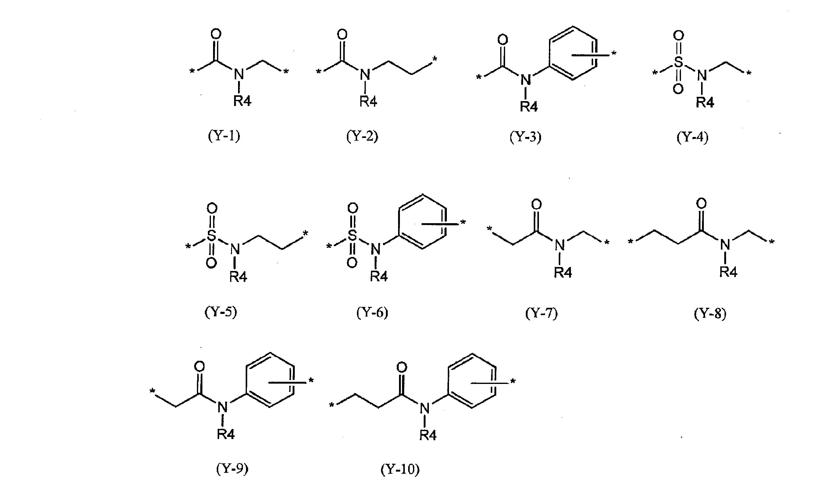


上記芳香族炭化水素環基としては、無置換芳香族炭化水素環基、脂肪族炭化水素基で置換された芳香族炭化水素環基等が挙げられ、上記芳香族ヘテロ環基としては、無置換芳香族ヘテロ環基、脂肪族炭化水素基で置換された芳香族ヘテロ環基等が挙げられる。
炭素原子数1~20の脂肪族炭化水素基としては、例えば、メチル、エチル、プロピル、イソプロピル、ブチル、s-ブチル、t-ブチル、イソブチル、アミル、イソアミル、t-アミル、ヘキシル、ヘプチル、イソヘプチル、t-ヘプチル、n-オクチル、イソオクチル、t-オクチル、ノニル、シクロプロピル、シクロブチル、シクロペンチル、シクロヘキシル、シクロヘプチル、シクロオクチル、シクロノニル、シクロデシル等の直鎖、分岐及び環状のアルキル基が挙げられ、炭素原子数1~20の脂肪族炭化水素基は、-O-、-COO-、-OCO-、-CO-、-S-、-SO-、-SO2-、-NR13-、-C=C-、-C≡C-で中断されていてもよく、R13は炭素原子数1~20の脂肪族炭化水素基であり、その例としては上記炭素原子数1~20の脂肪族炭化水素基と同じであり、中断する基に炭素原子を含む場合、中断される基を含めた炭素原子数が1~20である。
上記の置換されていてもよい脂肪族炭化水素基としては、例えば前述の炭素原子数1~20の脂肪族炭化水素基が挙げられ、それらを置換してもよい置換基は、芳香族炭化水素環基及び芳香族ヘテロ環基を置換してもよい基として挙げたものと同様である。
R7及びR8で表される上記の置換されていてもよい炭化水素基は、R1、R2及びR3で表される置換されていてもよい炭化水素基として後に挙げるものと同様である。
尚、以下には、置換基を有していないものを示しているが、上記の通り、A1は置換基を有していてもよく、A2中の水素原子は置換基で置換されていてもよい。また、以下のA(16)~(23)において、複数の環にまたがって記載されている結合手は、それらの環を構成する炭素原子のいずれかに結合することを意味する(以下同様)。

上記芳香族炭化水素基としては、フェニル、ナフチル、シクロヘキシルフェニル、ビフェニル、ターフェニル、フルオレイル、チオフェニルフェニル、フラニルフェニル、2’-フェニル-プロピルフェニル、ベンジル、ナフチルメチル等が挙げられ、上記脂肪族炭化水素基としては、例えばA1の説明で用いた炭素原子数1~20の脂肪族炭化水素基が挙げられ、上記脂肪族炭化水素基で置換された芳香族炭化水素基としては、上記脂肪族炭化水素基で置換されたフェニル、ナフチル、ベンジル等が挙げられる。
これらの炭化水素基を置換してもよい基としては、フッ素原子、塩素原子、臭素原子、ヨウ素原子、シアノ基、ニトロ基、水酸基、チオール基、-NR7R8基等が挙げられ、R7及びR8が表す基は、A2において説明したR7及びR8と同様である。
尚、下記部分構造(3)及び(3-1)~(3-12)において、A1からA2への結合手は記載を省略している。下記部分構造(3-1)~(3-12)においては、A1からA2への結合手は、芳香族炭化水素環及び芳香族ヘテロ環を構成するいずれの炭素原子に付いていてもよい。


上記部分構造(3)を表す(3-11)及び(3-12)において、M2の金属元素としては、4配位又は6配位が可能な金属が挙げられ、より好ましくはRu、Fe、Os、Cu、W、Cr、Mo、Ni、Pd、Pt、Co、Ir、Rh、Re、Mn、Znであり、更に好ましくはRu、Fe、Os、Cuであり、特に好ましくはRuである。


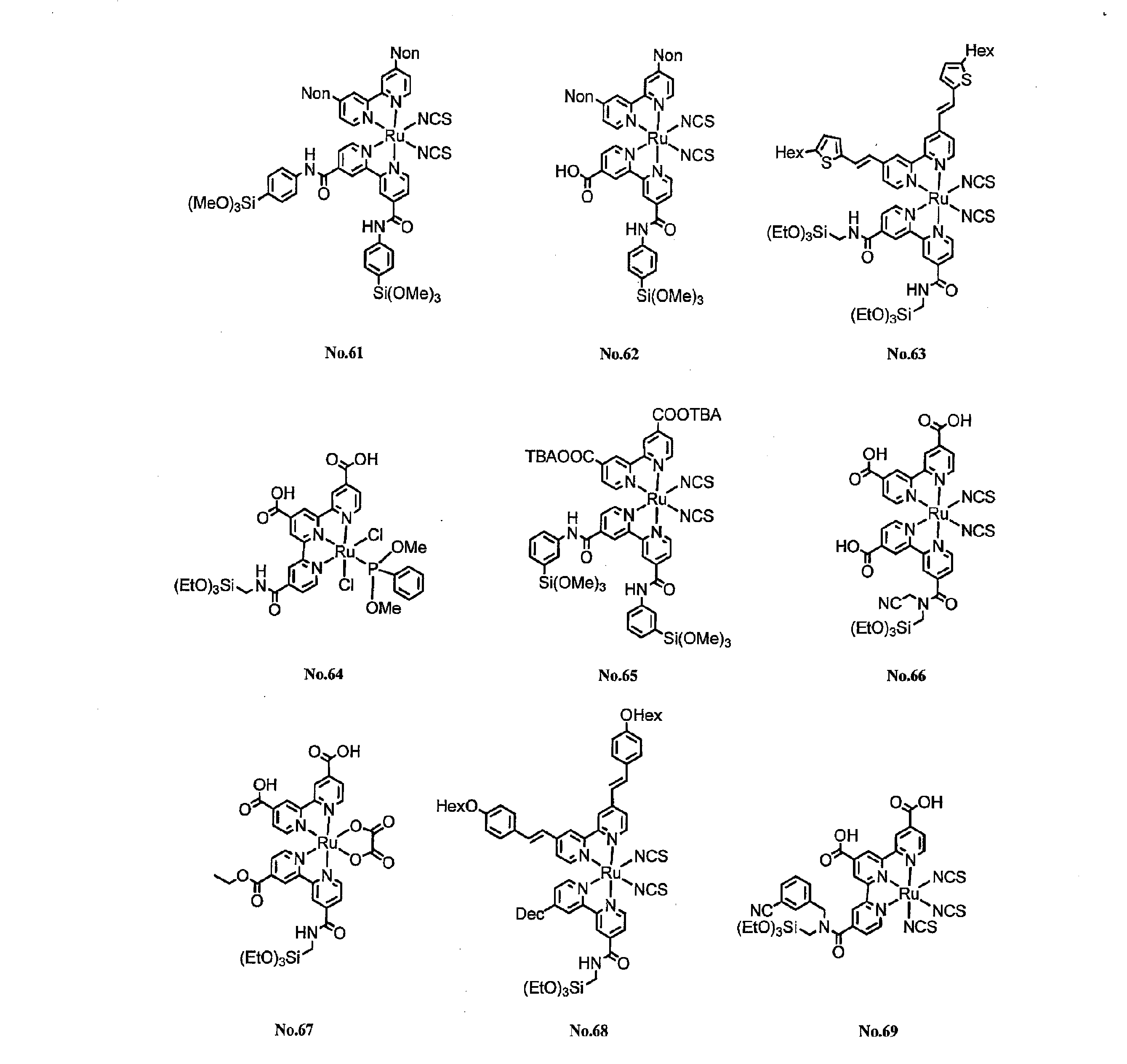

本発明の光電変換素子は、色素増感型光電変換素子であり、色素として本発明の新規化合物を用いる点以外は、従来の色素増感型光電変換素子と同様とすることができる。以下、本発明の光電変換素子の代表的な構成例について、図1及び図2を参照して説明する。
作用電極10は、外部回路に対して、負極として機能するものである。導電性基板11は、例えば、絶縁性の基板11Aの表面に導電層11Bを設けたものである。
有機金属錯体化合物としては、芳香族複素環内にある窒素アニオンと金属カチオンとで形成されるイオン性の配位結合と、窒素原子又はカルコゲン原子と金属カチオンとの間に形成される非イオン性配位結合の両方を有する有機金属錯体化合物や、酸素アニオン又は硫黄アニオンと金属カチオンとで形成されるイオン性の配位結合と、窒素原子又はカルコゲン原子と金属カチオンとの間に形成される非イオン性配位結合の両方を有する有機金属錯体化合物等が挙げられる。具体的には、銅フタロシアニン、チタニルフタロシアニン、コバルトフタロシアニン、ニッケルフタロシアニン、鉄フタロシアニン等の金属フタロシアニン系色素、金属ナフタロシアニン系色素、金属ポルフィリン系色素、金属アザポルフィリン系色素ならびにルテニウム、鉄、オスミウムを用いたビピリジル金属錯体、ターピリジル金属錯体、フェナントロリン金属錯体、ビシンコニン酸金属錯体、アゾ金属錯体あるいはキノリノール金属錯体等のルテニウム錯体等が挙げられる。

MK-2 Dye(シグマアルドリッチ製、0.10mmol、96mg)、塩化オキサリル(0.11mmol、14mg)、ジメチルホルムアミド(0.01ml)及びクロロホルム(2ml)をフラスコに仕込み、25℃で1時間撹拌した。10℃まで冷却した後、N,N-ジイソプロピルエチルアミン(0.20mmol、26mg)及び(トリエトキシシリルメチル)ヘキシルアミン(0.10mmol、28mg)を加えて、更に1時間撹拌した。反応液に水(2ml)を加え、油水分液を行った。得られた有機層をシリカゲルカラムクロマトグラフィー(移動相;クロロホルム)により精製することにより、紫色固体を108mg(収率89%)得た。得られた固体が、化合物No.1であることをUV-VIS(λmax)、1H-NMRを用いて確認した。データを〔表1〕及び〔表2-1〕に示す。
目的化合物に対応したカルボン酸又はスルホン酸を有する化合物及びアミン化合物を用いた以外は合成例1と同様の手法で化合物No.2~No.24、61、62、70~72を合成した。得られた化合物の外観及び収率を〔表1〕に示す。合成した化合物が目的化合物であることは、合成例1と同様に確認した。データを〔表1〕、〔表2-1〕、〔表2-2〕及び〔表2-3〕に示す。

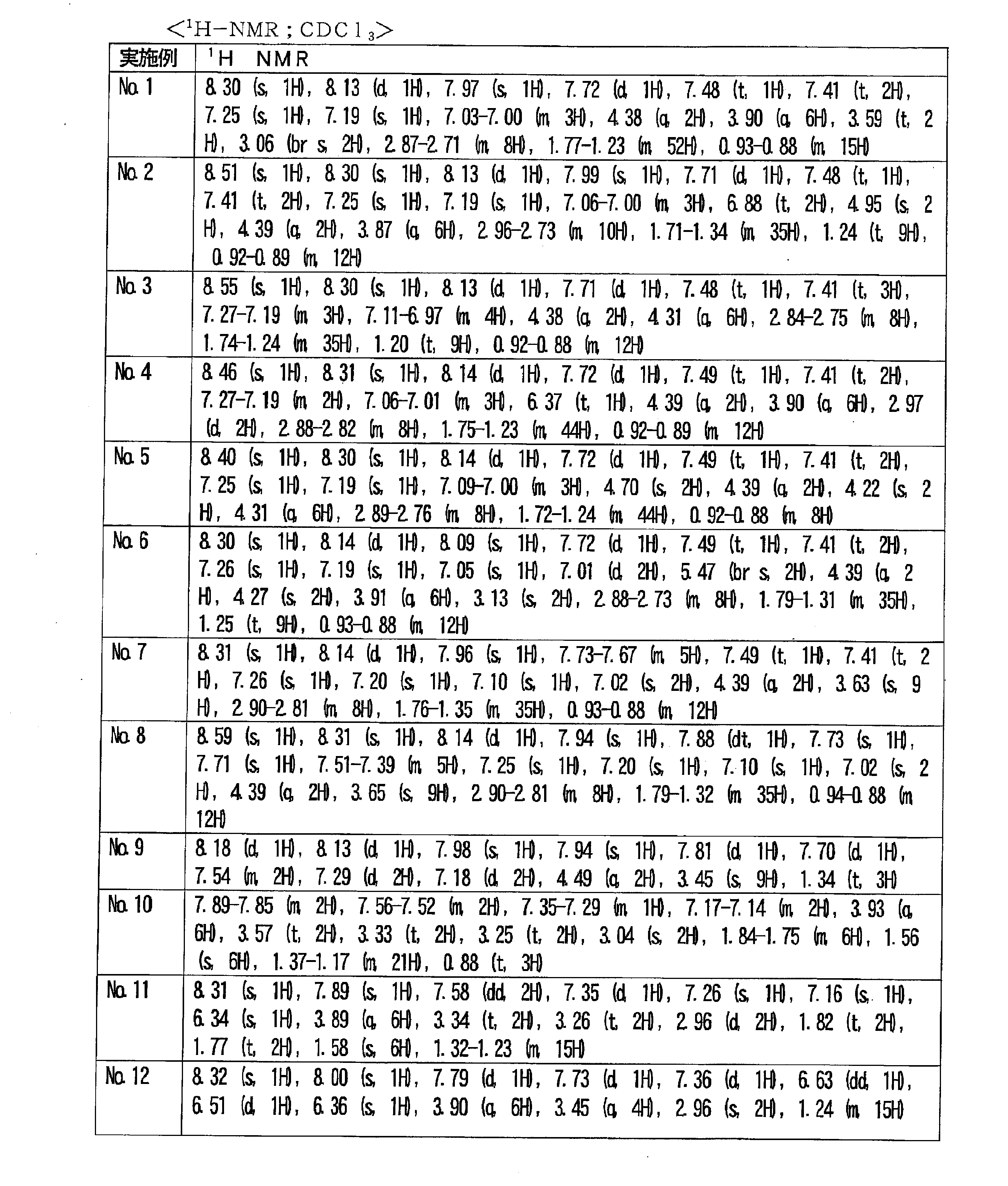


まず、縦2.0cm×横1.5cm×厚さ1.1mmの導電性ガラス基板(F-SnO2)よりなる導電性基板11を用意した。続いて、導電性基板11に、縦0.5cm×横0.5cmの四角形を囲むように厚さ70μmのマスキングテープを貼り、この部分に金属酸化物スラリー3cm3を一様の厚さとなるように塗布して乾燥させた。金属酸化物スラリーとしては、10重量%となるように酸化チタン粉末(TiO2、Solaronix社製Ti-NanoxideD)を、水に懸濁したものを用いた。続いて、導電性基板11上のマスキングテープを剥がし取り、この基板を電気炉により450℃で焼成し、厚さ約5μmの金属酸化物半導体層12を形成した。続いて、化合物No.1を3×10⁻⁴mol/dm3の濃度になるようにトルエンに溶解させて、色素溶液を調製した。続いて、金属酸化物半導体層12が形成された導電性基板11を上記の色素溶液に浸漬し、色素13を担持させた作用電極10を作製した。
作製した作用電極10を25℃、24時間の条件で、剥離液(アセトニトリル:水=99:1)に浸漬した。剥離液浸漬前の色素担持量(色素のλmaxにおけるAbs.)を100としたときの、剥離液浸漬後の色素担持量(剥離液浸漬前の色素担持量に対する割合)を、耐剥離性として〔表3〕に示した。剥離後の色素担持量が100に近いほど耐剥離性が高いといえる。
化合物No.1を〔表3〕の化合物に替えた以外は実施例1と同様の操作により、各化合物を担持させた作用電極10を作製し、色素の耐剥離性を求めた。結果を〔表3〕に示す。

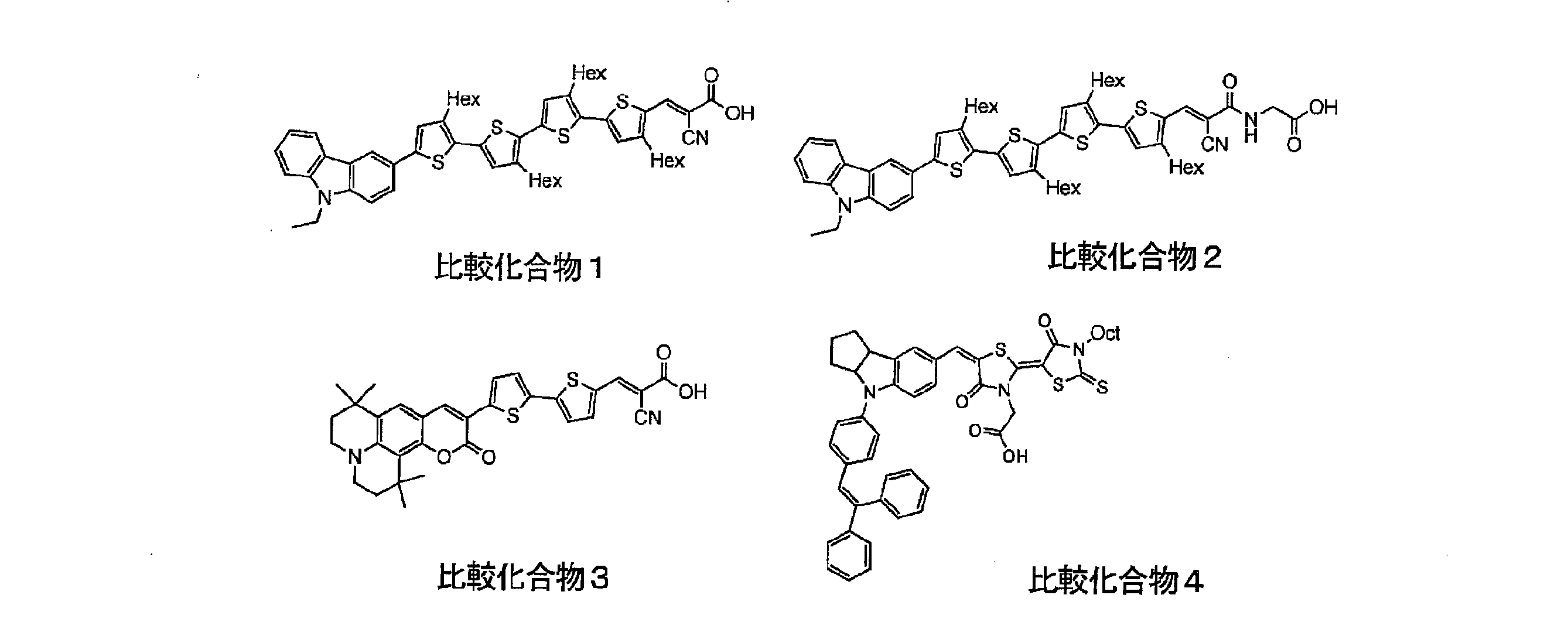
(実施例30~42及び比較例5~8)
図1に示すように、上記実施例1~11、27~29及び比較例1~4で作製した担持体(作用電極)を用いた作用電極10と、導電性基板21としてITO電極(西野田電工(株)製)上に黒鉛微粒子(導電層22)をコーティングして作製した対向電極20とを、スペーサー(63μm)を介して対向させ、それらの間に電解質含有層30を配し、これらをクリップで固定し、電解質含有層30に電解液〔アセトニトリルに対して、4-t-ブチルピリジン(0.5mol/dm3)、ヨウ化リチウム(0.5mol/dm3)、ヨウ素(0.05mol/dm3)を、それぞれ所定の濃度になるように混合したもの〕を浸透させ、光電変換素子を作製した。セル上部を開口部1cm2のマスクで覆い、AM-1.5(1000W/m2)のソーラーシミュレーターを用いて変換効率を測定した。結果を、〔表4〕に示す。

(実施例43~45及び比較例9)
化合物No.1を〔表4A〕の化合物に替え、酸化チタン粉末を酸化亜鉛(ZnO、ソーラー社製)に変更した以外は実施例1と同様の操作により、各化合物を担持させた作用電極10を作製した。得られた作用電極10を用いて、実施例30と同様の操作により変換効率を測定した。結果を〔表4A〕に示す。

上記実施例4、7及び比較例1、2で作製した担持体(作用電極)について耐光性評価を行った。評価は、該作用電極に55000ルクスの光を4時間照射し、UV吸収スペクトルのλmaxの変化を、照射前を100として算出した。具体的には、λmaxにおける照射後のAbs.及び照射前のAbs.を測定し、「(照射後のAbs./照射前のAbs.)×100」を求め、耐光性の値とした。結果を〔表5〕に示す。
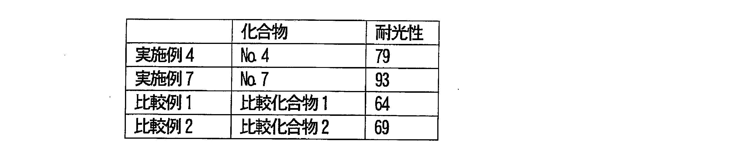
Claims (8)
- 下記一般式(1)で表される新規化合物。

但し、Yは、下記の部分構造式(Y-11)及び(Y-12)で表わされる基を除く。)

- 上記一般式(1)におけるR1、R2及びR3が、直鎖又は分岐鎖脂肪族炭化水素オキシ基である請求項1に記載の新規化合物。
- 上記一般式(1)におけるYが、下記部分構造式(Y-1)~(Y-10)から選ばれる基である請求項1又は2に記載の新規化合物。

- 上記一般式(1)におけるZが、下記部分構造式(2)で表される請求項1~3の何れか一項に記載の新規化合物。


- 上記部分構造式(2)中の下記部分構造(3)が、下記部分構造(3-1)~(3-12)の何れかである請求項1~4の何れか一項に記載の新規化合物。

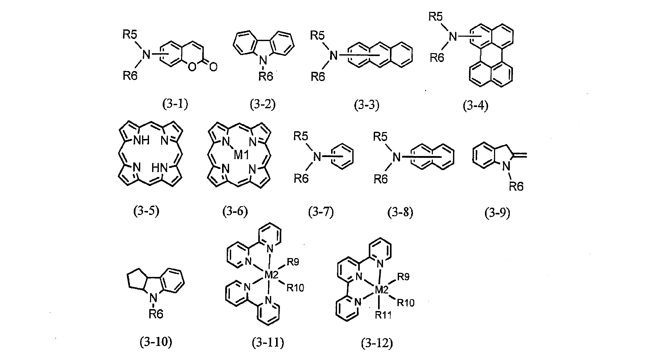
- 下記一般式(1)で表される化合物を担持した担持体。

- 上記一般式(1)におけるR1、R2及びR3が、直鎖又は分岐鎖脂肪族炭化水素オキシ基である請求項6に記載の担持体。
- 請求項6又は7に記載の担持体を有する電極を備えた光電変換素子。
Priority Applications (5)
| Application Number | Priority Date | Filing Date | Title |
|---|---|---|---|
| EP12849937.3A EP2781555A4 (en) | 2011-11-18 | 2012-08-21 | NEW COMPOUND AND SUPPORT SUPPORTING THIS NEW COMPOUND |
| JP2013544156A JP6145407B2 (ja) | 2011-11-18 | 2012-08-21 | 新規化合物及びこの新規化合物を担持した担持体 |
| CN201280046590.0A CN103827126B (zh) | 2011-11-18 | 2012-08-21 | 新型化合物和担载该新型化合物的担载体 |
| US14/350,171 US9530571B2 (en) | 2011-11-18 | 2012-08-21 | Compound and support material supporting this novel compound |
| KR1020147008991A KR20140094507A (ko) | 2011-11-18 | 2012-08-21 | 신규 화합물 및 이 신규 화합물을 담지한 담지체 |
Applications Claiming Priority (2)
| Application Number | Priority Date | Filing Date | Title |
|---|---|---|---|
| JP2011253132 | 2011-11-18 | ||
| JP2011-253132 | 2011-11-18 |
Publications (1)
| Publication Number | Publication Date |
|---|---|
| WO2013073243A1 true WO2013073243A1 (ja) | 2013-05-23 |
Family
ID=48429324
Family Applications (1)
| Application Number | Title | Priority Date | Filing Date |
|---|---|---|---|
| PCT/JP2012/071093 WO2013073243A1 (ja) | 2011-11-18 | 2012-08-21 | 新規化合物及びこの新規化合物を担持した担持体 |
Country Status (7)
| Country | Link |
|---|---|
| US (1) | US9530571B2 (ja) |
| EP (1) | EP2781555A4 (ja) |
| JP (1) | JP6145407B2 (ja) |
| KR (1) | KR20140094507A (ja) |
| CN (1) | CN103827126B (ja) |
| TW (1) | TWI598354B (ja) |
| WO (1) | WO2013073243A1 (ja) |
Cited By (1)
| Publication number | Priority date | Publication date | Assignee | Title |
|---|---|---|---|---|
| ITMI20131621A1 (it) * | 2013-10-01 | 2015-04-02 | Cnrs Ct Nat De La Rech He Scient | Colorante organico per una cella solare sensibilizzata con colorante |
Families Citing this family (5)
| Publication number | Priority date | Publication date | Assignee | Title |
|---|---|---|---|---|
| US9324889B2 (en) * | 2011-04-05 | 2016-04-26 | Adeka Corporation | Compound and photoelectric conversion device |
| EP2940781A4 (en) * | 2012-12-28 | 2016-08-17 | Adeka Corp | LOADED BODY AND PHOTOELECTRIC CONVERSION ELEMENT |
| JPWO2016171153A1 (ja) * | 2015-04-21 | 2018-02-22 | 住友精化株式会社 | 色素増感太陽電池および色素増感太陽電池用電解液 |
| CN111180793B (zh) * | 2020-02-16 | 2021-01-26 | 双登集团股份有限公司 | 一种用于锂电池的防过充安全电解液 |
| GB2618763A (en) * | 2022-03-22 | 2023-11-22 | Ali Fadda Ahmed | Improved three dyes lifelong and low cost solar cells |
Citations (12)
| Publication number | Priority date | Publication date | Assignee | Title |
|---|---|---|---|---|
| CS215229B1 (cs) * | 1981-01-04 | 1982-08-27 | Stanislav Florovic | BLá/trialkoxysilyl/ amidoámóniové .soli a sposob ich přípravy |
| JPH07307133A (ja) * | 1994-03-18 | 1995-11-21 | Hitachi Ltd | 表示装置とそれに用いる波長選択吸収膜用材料およびその製法 |
| JPH08259543A (ja) | 1994-12-21 | 1996-10-08 | Asulab Sa | 疎水性液状塩とその生成法ならびに電気化学への応用 |
| JPH09507334A (ja) | 1993-02-03 | 1997-07-22 | エコール ポリテクニーク フェデラル ドゥ ローザンヌ | 光電気化学電池及びこの電池用の電解液 |
| JP2003168493A (ja) | 2001-11-30 | 2003-06-13 | Tdk Corp | 色素増感型太陽電池 |
| JP2003331936A (ja) | 2002-05-13 | 2003-11-21 | National Institute Of Advanced Industrial & Technology | ピリジン及び/又はピリジン系化合物を含む電解質溶液を用いた光電変換素子及びそれを用いた色素増感型太陽電池 |
| JP2005093313A (ja) | 2003-09-19 | 2005-04-07 | Toyo Ink Mfg Co Ltd | 色素増感型光電変換素子用電解質組成物、それを用いた光電変換素子。 |
| JP2009221059A (ja) * | 2008-03-17 | 2009-10-01 | Furukawa Electric Co Ltd:The | 積層構造のシリカナノ粒子の製造方法、積層構造のシリカナノ粒子、及びそれを用いた標識試薬 |
| JP2010526897A (ja) * | 2007-05-11 | 2010-08-05 | ビーエーエスエフ ソシエタス・ヨーロピア | 高分子色素 |
| JP2011108527A (ja) * | 2009-11-18 | 2011-06-02 | Institute Of Systems Information Technologies & Nanotechnologies | デバイス、薄膜トランジスタおよびその製造方法 |
| JP2011122088A (ja) | 2009-12-11 | 2011-06-23 | National Institute Of Advanced Industrial Science & Technology | 有機色素化合物及びそれを用いた半導体薄膜電極、光電変換素子、光電気化学太陽電池 |
| JP2011132163A (ja) | 2009-12-24 | 2011-07-07 | Shin-Etsu Chemical Co Ltd | 反応性シリル基を有するトリアリールアミン誘導体及び無機材料並びに色素増感型光電変換素子 |
Family Cites Families (12)
| Publication number | Priority date | Publication date | Assignee | Title |
|---|---|---|---|---|
| US4460739A (en) | 1983-07-01 | 1984-07-17 | General Electric Company | Composition for promoting adhesion of curable silicones to substrates |
| JP3524617B2 (ja) * | 1995-03-13 | 2004-05-10 | 新日本石油株式会社 | 紫外線吸収剤及びコーティング材料 |
| ATE324943T1 (de) | 1999-09-20 | 2006-06-15 | Penn State Res Found | Chirale phosphine, deren komplexe mit übergangsmetallen und deren verwendung in asymmetrischen synthesereaktionen |
| JP4912561B2 (ja) * | 2000-08-03 | 2012-04-11 | チバ ホールディング インコーポレーテッド | 光に安定なシリル化ベンゾトリアゾールuv吸収剤及びそれにより安定化された組成物 |
| US20050287560A1 (en) | 2001-07-13 | 2005-12-29 | Nanosphere, Inc. | Method for preparing substrates having immobilized molecules and substrates |
| AU2002322458A1 (en) | 2001-07-13 | 2003-01-29 | Nanosphere, Inc. | Method for immobilizing molecules onto surfaces |
| DE60310521T2 (de) | 2002-01-22 | 2007-11-08 | Universiteit Gent | Metallkomplexe für die metathese |
| JP4648944B2 (ja) * | 2004-05-06 | 2011-03-09 | ナノスフェアー インコーポレイテッド | 分子が固定化された基材を製造する方法および基材 |
| EP2144918B1 (en) * | 2007-05-11 | 2010-11-17 | Basf Se | Functionalized nanoparticles |
| CN101050223B (zh) | 2007-05-14 | 2010-12-01 | 张群朝 | 含硅烷或功能聚硅氧烷改性的异氰酸酯类三聚体及其制备方法 |
| WO2009038659A2 (en) * | 2007-09-14 | 2009-03-26 | Health Research, Inc. | Organically modified silica nanoparticles with covalently incorporated photosensitizers for drug delivery in photodynamic therapy |
| CN102498157A (zh) | 2009-04-29 | 2012-06-13 | 汉高公司 | 湿气固化性聚二硫醚 |
-
2012
- 2012-08-21 CN CN201280046590.0A patent/CN103827126B/zh not_active Expired - Fee Related
- 2012-08-21 EP EP12849937.3A patent/EP2781555A4/en not_active Withdrawn
- 2012-08-21 US US14/350,171 patent/US9530571B2/en not_active Expired - Fee Related
- 2012-08-21 KR KR1020147008991A patent/KR20140094507A/ko active IP Right Grant
- 2012-08-21 WO PCT/JP2012/071093 patent/WO2013073243A1/ja active Application Filing
- 2012-08-21 JP JP2013544156A patent/JP6145407B2/ja not_active Expired - Fee Related
- 2012-09-05 TW TW101132415A patent/TWI598354B/zh not_active IP Right Cessation
Patent Citations (12)
| Publication number | Priority date | Publication date | Assignee | Title |
|---|---|---|---|---|
| CS215229B1 (cs) * | 1981-01-04 | 1982-08-27 | Stanislav Florovic | BLá/trialkoxysilyl/ amidoámóniové .soli a sposob ich přípravy |
| JPH09507334A (ja) | 1993-02-03 | 1997-07-22 | エコール ポリテクニーク フェデラル ドゥ ローザンヌ | 光電気化学電池及びこの電池用の電解液 |
| JPH07307133A (ja) * | 1994-03-18 | 1995-11-21 | Hitachi Ltd | 表示装置とそれに用いる波長選択吸収膜用材料およびその製法 |
| JPH08259543A (ja) | 1994-12-21 | 1996-10-08 | Asulab Sa | 疎水性液状塩とその生成法ならびに電気化学への応用 |
| JP2003168493A (ja) | 2001-11-30 | 2003-06-13 | Tdk Corp | 色素増感型太陽電池 |
| JP2003331936A (ja) | 2002-05-13 | 2003-11-21 | National Institute Of Advanced Industrial & Technology | ピリジン及び/又はピリジン系化合物を含む電解質溶液を用いた光電変換素子及びそれを用いた色素増感型太陽電池 |
| JP2005093313A (ja) | 2003-09-19 | 2005-04-07 | Toyo Ink Mfg Co Ltd | 色素増感型光電変換素子用電解質組成物、それを用いた光電変換素子。 |
| JP2010526897A (ja) * | 2007-05-11 | 2010-08-05 | ビーエーエスエフ ソシエタス・ヨーロピア | 高分子色素 |
| JP2009221059A (ja) * | 2008-03-17 | 2009-10-01 | Furukawa Electric Co Ltd:The | 積層構造のシリカナノ粒子の製造方法、積層構造のシリカナノ粒子、及びそれを用いた標識試薬 |
| JP2011108527A (ja) * | 2009-11-18 | 2011-06-02 | Institute Of Systems Information Technologies & Nanotechnologies | デバイス、薄膜トランジスタおよびその製造方法 |
| JP2011122088A (ja) | 2009-12-11 | 2011-06-23 | National Institute Of Advanced Industrial Science & Technology | 有機色素化合物及びそれを用いた半導体薄膜電極、光電変換素子、光電気化学太陽電池 |
| JP2011132163A (ja) | 2009-12-24 | 2011-07-07 | Shin-Etsu Chemical Co Ltd | 反応性シリル基を有するトリアリールアミン誘導体及び無機材料並びに色素増感型光電変換素子 |
Non-Patent Citations (3)
| Title |
|---|
| ELECTROCHEMISTRY, vol. 2, 2002, pages 130 - 136 |
| INORG. CHEM., vol. 35, 1996, pages 1168 - 1178 |
| See also references of EP2781555A4 |
Cited By (3)
| Publication number | Priority date | Publication date | Assignee | Title |
|---|---|---|---|---|
| ITMI20131621A1 (it) * | 2013-10-01 | 2015-04-02 | Cnrs Ct Nat De La Rech He Scient | Colorante organico per una cella solare sensibilizzata con colorante |
| WO2015049640A3 (en) * | 2013-10-01 | 2015-08-06 | Eni S.P.A. | Organic dye for a dye-sensitized solar cell |
| US9997299B2 (en) | 2013-10-01 | 2018-06-12 | Eni S.P.A. | Organic dye for a dye-sensitized solar cell |
Also Published As
| Publication number | Publication date |
|---|---|
| TW201321391A (zh) | 2013-06-01 |
| US20140261647A1 (en) | 2014-09-18 |
| EP2781555A1 (en) | 2014-09-24 |
| JPWO2013073243A1 (ja) | 2015-04-02 |
| CN103827126B (zh) | 2017-05-17 |
| TWI598354B (zh) | 2017-09-11 |
| KR20140094507A (ko) | 2014-07-30 |
| CN103827126A (zh) | 2014-05-28 |
| EP2781555A4 (en) | 2015-10-07 |
| US9530571B2 (en) | 2016-12-27 |
| JP6145407B2 (ja) | 2017-06-14 |
Similar Documents
| Publication | Publication Date | Title |
|---|---|---|
| JP6145407B2 (ja) | 新規化合物及びこの新規化合物を担持した担持体 | |
| WO2014103831A1 (ja) | 担持体及び光電変換素子 | |
| EP2800199B1 (en) | Dye-sensitized solar cell | |
| JPWO2010038589A1 (ja) | 光電変換素子用色素および光電変換素子 | |
| US9812263B2 (en) | Compound and photoelectric conversion device | |
| JP6113713B2 (ja) | 新規化合物及びこの新規化合物を担持した担持体 | |
| WO2015178257A1 (ja) | 担持方法、担持体及び光電変換素子 | |
| WO2016108269A1 (ja) | 化合物、担持体及び光電変換素子 | |
| JP2016219653A (ja) | 担持体及び光電変換素子 |
Legal Events
| Date | Code | Title | Description |
|---|---|---|---|
| 121 | Ep: the epo has been informed by wipo that ep was designated in this application |
Ref document number: 12849937 Country of ref document: EP Kind code of ref document: A1 |
|
| ENP | Entry into the national phase |
Ref document number: 2013544156 Country of ref document: JP Kind code of ref document: A |
|
| WWE | Wipo information: entry into national phase |
Ref document number: 2012849937 Country of ref document: EP |
|
| ENP | Entry into the national phase |
Ref document number: 20147008991 Country of ref document: KR Kind code of ref document: A |
|
| WWE | Wipo information: entry into national phase |
Ref document number: 14350171 Country of ref document: US |
|
| NENP | Non-entry into the national phase |
Ref country code: DE |