WO2013065474A1 - 半導体装置 - Google Patents
半導体装置 Download PDFInfo
- Publication number
- WO2013065474A1 WO2013065474A1 PCT/JP2012/076685 JP2012076685W WO2013065474A1 WO 2013065474 A1 WO2013065474 A1 WO 2013065474A1 JP 2012076685 W JP2012076685 W JP 2012076685W WO 2013065474 A1 WO2013065474 A1 WO 2013065474A1
- Authority
- WO
- WIPO (PCT)
- Prior art keywords
- die pad
- semiconductor device
- back surface
- layer
- bonding
- Prior art date
- Legal status (The legal status is an assumption and is not a legal conclusion. Google has not performed a legal analysis and makes no representation as to the accuracy of the status listed.)
- Ceased
Links
Images


























Classifications
-
- H—ELECTRICITY
- H10—SEMICONDUCTOR DEVICES; ELECTRIC SOLID-STATE DEVICES NOT OTHERWISE PROVIDED FOR
- H10W—GENERIC PACKAGES, INTERCONNECTIONS, CONNECTORS OR OTHER CONSTRUCTIONAL DETAILS OF DEVICES COVERED BY CLASS H10
- H10W40/00—Arrangements for thermal protection or thermal control
- H10W40/20—Arrangements for cooling
- H10W40/25—Arrangements for cooling characterised by their materials
- H10W40/258—Metallic materials
-
- H—ELECTRICITY
- H10—SEMICONDUCTOR DEVICES; ELECTRIC SOLID-STATE DEVICES NOT OTHERWISE PROVIDED FOR
- H10W—GENERIC PACKAGES, INTERCONNECTIONS, CONNECTORS OR OTHER CONSTRUCTIONAL DETAILS OF DEVICES COVERED BY CLASS H10
- H10W40/00—Arrangements for thermal protection or thermal control
- H10W40/20—Arrangements for cooling
- H10W40/25—Arrangements for cooling characterised by their materials
- H10W40/259—Ceramics or glasses
-
- H—ELECTRICITY
- H10—SEMICONDUCTOR DEVICES; ELECTRIC SOLID-STATE DEVICES NOT OTHERWISE PROVIDED FOR
- H10W—GENERIC PACKAGES, INTERCONNECTIONS, CONNECTORS OR OTHER CONSTRUCTIONAL DETAILS OF DEVICES COVERED BY CLASS H10
- H10W40/00—Arrangements for thermal protection or thermal control
- H10W40/70—Fillings or auxiliary members in containers or in encapsulations for thermal protection or control
- H10W40/77—Auxiliary members characterised by their shape
- H10W40/778—Auxiliary members characterised by their shape in encapsulations
-
- H—ELECTRICITY
- H10—SEMICONDUCTOR DEVICES; ELECTRIC SOLID-STATE DEVICES NOT OTHERWISE PROVIDED FOR
- H10W—GENERIC PACKAGES, INTERCONNECTIONS, CONNECTORS OR OTHER CONSTRUCTIONAL DETAILS OF DEVICES COVERED BY CLASS H10
- H10W70/00—Package substrates; Interposers; Redistribution layers [RDL]
- H10W70/40—Leadframes
- H10W70/411—Chip-supporting parts, e.g. die pads
-
- H—ELECTRICITY
- H10—SEMICONDUCTOR DEVICES; ELECTRIC SOLID-STATE DEVICES NOT OTHERWISE PROVIDED FOR
- H10W—GENERIC PACKAGES, INTERCONNECTIONS, CONNECTORS OR OTHER CONSTRUCTIONAL DETAILS OF DEVICES COVERED BY CLASS H10
- H10W70/00—Package substrates; Interposers; Redistribution layers [RDL]
- H10W70/40—Leadframes
- H10W70/411—Chip-supporting parts, e.g. die pads
- H10W70/417—Bonding materials between chips and die pads
-
- H—ELECTRICITY
- H10—SEMICONDUCTOR DEVICES; ELECTRIC SOLID-STATE DEVICES NOT OTHERWISE PROVIDED FOR
- H10W—GENERIC PACKAGES, INTERCONNECTIONS, CONNECTORS OR OTHER CONSTRUCTIONAL DETAILS OF DEVICES COVERED BY CLASS H10
- H10W70/00—Package substrates; Interposers; Redistribution layers [RDL]
- H10W70/40—Leadframes
- H10W70/421—Shapes or dispositions
-
- H—ELECTRICITY
- H10—SEMICONDUCTOR DEVICES; ELECTRIC SOLID-STATE DEVICES NOT OTHERWISE PROVIDED FOR
- H10W—GENERIC PACKAGES, INTERCONNECTIONS, CONNECTORS OR OTHER CONSTRUCTIONAL DETAILS OF DEVICES COVERED BY CLASS H10
- H10W70/00—Package substrates; Interposers; Redistribution layers [RDL]
- H10W70/40—Leadframes
- H10W70/421—Shapes or dispositions
- H10W70/424—Cross-sectional shapes
- H10W70/427—Bent parts
-
- H—ELECTRICITY
- H10—SEMICONDUCTOR DEVICES; ELECTRIC SOLID-STATE DEVICES NOT OTHERWISE PROVIDED FOR
- H10W—GENERIC PACKAGES, INTERCONNECTIONS, CONNECTORS OR OTHER CONSTRUCTIONAL DETAILS OF DEVICES COVERED BY CLASS H10
- H10W70/00—Package substrates; Interposers; Redistribution layers [RDL]
- H10W70/40—Leadframes
- H10W70/456—Materials
- H10W70/457—Materials of metallic layers on leadframes
-
- H—ELECTRICITY
- H10—SEMICONDUCTOR DEVICES; ELECTRIC SOLID-STATE DEVICES NOT OTHERWISE PROVIDED FOR
- H10W—GENERIC PACKAGES, INTERCONNECTIONS, CONNECTORS OR OTHER CONSTRUCTIONAL DETAILS OF DEVICES COVERED BY CLASS H10
- H10W70/00—Package substrates; Interposers; Redistribution layers [RDL]
- H10W70/40—Leadframes
- H10W70/461—Leadframes specially adapted for cooling
-
- H—ELECTRICITY
- H10—SEMICONDUCTOR DEVICES; ELECTRIC SOLID-STATE DEVICES NOT OTHERWISE PROVIDED FOR
- H10W—GENERIC PACKAGES, INTERCONNECTIONS, CONNECTORS OR OTHER CONSTRUCTIONAL DETAILS OF DEVICES COVERED BY CLASS H10
- H10W72/00—Interconnections or connectors in packages
- H10W72/071—Connecting or disconnecting
- H10W72/072—Connecting or disconnecting of bump connectors
-
- H—ELECTRICITY
- H10—SEMICONDUCTOR DEVICES; ELECTRIC SOLID-STATE DEVICES NOT OTHERWISE PROVIDED FOR
- H10W—GENERIC PACKAGES, INTERCONNECTIONS, CONNECTORS OR OTHER CONSTRUCTIONAL DETAILS OF DEVICES COVERED BY CLASS H10
- H10W74/00—Encapsulations, e.g. protective coatings
- H10W74/10—Encapsulations, e.g. protective coatings characterised by their shape or disposition
- H10W74/111—Encapsulations, e.g. protective coatings characterised by their shape or disposition the semiconductor body being completely enclosed
-
- H—ELECTRICITY
- H10—SEMICONDUCTOR DEVICES; ELECTRIC SOLID-STATE DEVICES NOT OTHERWISE PROVIDED FOR
- H10W—GENERIC PACKAGES, INTERCONNECTIONS, CONNECTORS OR OTHER CONSTRUCTIONAL DETAILS OF DEVICES COVERED BY CLASS H10
- H10W74/00—Encapsulations, e.g. protective coatings
- H10W74/10—Encapsulations, e.g. protective coatings characterised by their shape or disposition
- H10W74/111—Encapsulations, e.g. protective coatings characterised by their shape or disposition the semiconductor body being completely enclosed
- H10W74/114—Encapsulations, e.g. protective coatings characterised by their shape or disposition the semiconductor body being completely enclosed by a substrate and the encapsulations
-
- H—ELECTRICITY
- H10—SEMICONDUCTOR DEVICES; ELECTRIC SOLID-STATE DEVICES NOT OTHERWISE PROVIDED FOR
- H10W—GENERIC PACKAGES, INTERCONNECTIONS, CONNECTORS OR OTHER CONSTRUCTIONAL DETAILS OF DEVICES COVERED BY CLASS H10
- H10W90/00—Package configurations
- H10W90/811—Multiple chips on leadframes
-
- H—ELECTRICITY
- H10—SEMICONDUCTOR DEVICES; ELECTRIC SOLID-STATE DEVICES NOT OTHERWISE PROVIDED FOR
- H10W—GENERIC PACKAGES, INTERCONNECTIONS, CONNECTORS OR OTHER CONSTRUCTIONAL DETAILS OF DEVICES COVERED BY CLASS H10
- H10W40/00—Arrangements for thermal protection or thermal control
- H10W40/20—Arrangements for cooling
- H10W40/22—Arrangements for cooling characterised by their shape, e.g. having conical or cylindrical projections
-
- H—ELECTRICITY
- H10—SEMICONDUCTOR DEVICES; ELECTRIC SOLID-STATE DEVICES NOT OTHERWISE PROVIDED FOR
- H10W—GENERIC PACKAGES, INTERCONNECTIONS, CONNECTORS OR OTHER CONSTRUCTIONAL DETAILS OF DEVICES COVERED BY CLASS H10
- H10W72/00—Interconnections or connectors in packages
- H10W72/071—Connecting or disconnecting
- H10W72/0711—Apparatus therefor
- H10W72/07141—Means for applying energy, e.g. ovens or lasers
-
- H—ELECTRICITY
- H10—SEMICONDUCTOR DEVICES; ELECTRIC SOLID-STATE DEVICES NOT OTHERWISE PROVIDED FOR
- H10W—GENERIC PACKAGES, INTERCONNECTIONS, CONNECTORS OR OTHER CONSTRUCTIONAL DETAILS OF DEVICES COVERED BY CLASS H10
- H10W72/00—Interconnections or connectors in packages
- H10W72/071—Connecting or disconnecting
- H10W72/073—Connecting or disconnecting of die-attach connectors
-
- H—ELECTRICITY
- H10—SEMICONDUCTOR DEVICES; ELECTRIC SOLID-STATE DEVICES NOT OTHERWISE PROVIDED FOR
- H10W—GENERIC PACKAGES, INTERCONNECTIONS, CONNECTORS OR OTHER CONSTRUCTIONAL DETAILS OF DEVICES COVERED BY CLASS H10
- H10W72/00—Interconnections or connectors in packages
- H10W72/071—Connecting or disconnecting
- H10W72/075—Connecting or disconnecting of bond wires
-
- H—ELECTRICITY
- H10—SEMICONDUCTOR DEVICES; ELECTRIC SOLID-STATE DEVICES NOT OTHERWISE PROVIDED FOR
- H10W—GENERIC PACKAGES, INTERCONNECTIONS, CONNECTORS OR OTHER CONSTRUCTIONAL DETAILS OF DEVICES COVERED BY CLASS H10
- H10W72/00—Interconnections or connectors in packages
- H10W72/071—Connecting or disconnecting
- H10W72/075—Connecting or disconnecting of bond wires
- H10W72/07521—Aligning
-
- H—ELECTRICITY
- H10—SEMICONDUCTOR DEVICES; ELECTRIC SOLID-STATE DEVICES NOT OTHERWISE PROVIDED FOR
- H10W—GENERIC PACKAGES, INTERCONNECTIONS, CONNECTORS OR OTHER CONSTRUCTIONAL DETAILS OF DEVICES COVERED BY CLASS H10
- H10W72/00—Interconnections or connectors in packages
- H10W72/071—Connecting or disconnecting
- H10W72/075—Connecting or disconnecting of bond wires
- H10W72/07551—Connecting or disconnecting of bond wires characterised by changes in properties of the bond wires during the connecting
- H10W72/07554—Connecting or disconnecting of bond wires characterised by changes in properties of the bond wires during the connecting changes in dispositions
-
- H—ELECTRICITY
- H10—SEMICONDUCTOR DEVICES; ELECTRIC SOLID-STATE DEVICES NOT OTHERWISE PROVIDED FOR
- H10W—GENERIC PACKAGES, INTERCONNECTIONS, CONNECTORS OR OTHER CONSTRUCTIONAL DETAILS OF DEVICES COVERED BY CLASS H10
- H10W72/00—Interconnections or connectors in packages
- H10W72/071—Connecting or disconnecting
- H10W72/075—Connecting or disconnecting of bond wires
- H10W72/07551—Connecting or disconnecting of bond wires characterised by changes in properties of the bond wires during the connecting
- H10W72/07555—Connecting or disconnecting of bond wires characterised by changes in properties of the bond wires during the connecting changes in materials
-
- H—ELECTRICITY
- H10—SEMICONDUCTOR DEVICES; ELECTRIC SOLID-STATE DEVICES NOT OTHERWISE PROVIDED FOR
- H10W—GENERIC PACKAGES, INTERCONNECTIONS, CONNECTORS OR OTHER CONSTRUCTIONAL DETAILS OF DEVICES COVERED BY CLASS H10
- H10W72/00—Interconnections or connectors in packages
- H10W72/20—Bump connectors, e.g. solder bumps or copper pillars; Dummy bumps; Thermal bumps
- H10W72/241—Dispositions, e.g. layouts
- H10W72/244—Dispositions, e.g. layouts relative to underlying supporting features, e.g. bond pads, RDLs or vias
-
- H—ELECTRICITY
- H10—SEMICONDUCTOR DEVICES; ELECTRIC SOLID-STATE DEVICES NOT OTHERWISE PROVIDED FOR
- H10W—GENERIC PACKAGES, INTERCONNECTIONS, CONNECTORS OR OTHER CONSTRUCTIONAL DETAILS OF DEVICES COVERED BY CLASS H10
- H10W72/00—Interconnections or connectors in packages
- H10W72/20—Bump connectors, e.g. solder bumps or copper pillars; Dummy bumps; Thermal bumps
- H10W72/241—Dispositions, e.g. layouts
- H10W72/247—Dispositions of multiple bumps
-
- H—ELECTRICITY
- H10—SEMICONDUCTOR DEVICES; ELECTRIC SOLID-STATE DEVICES NOT OTHERWISE PROVIDED FOR
- H10W—GENERIC PACKAGES, INTERCONNECTIONS, CONNECTORS OR OTHER CONSTRUCTIONAL DETAILS OF DEVICES COVERED BY CLASS H10
- H10W72/00—Interconnections or connectors in packages
- H10W72/20—Bump connectors, e.g. solder bumps or copper pillars; Dummy bumps; Thermal bumps
- H10W72/241—Dispositions, e.g. layouts
- H10W72/247—Dispositions of multiple bumps
- H10W72/248—Top-view layouts, e.g. mirror arrays
-
- H—ELECTRICITY
- H10—SEMICONDUCTOR DEVICES; ELECTRIC SOLID-STATE DEVICES NOT OTHERWISE PROVIDED FOR
- H10W—GENERIC PACKAGES, INTERCONNECTIONS, CONNECTORS OR OTHER CONSTRUCTIONAL DETAILS OF DEVICES COVERED BY CLASS H10
- H10W72/00—Interconnections or connectors in packages
- H10W72/20—Bump connectors, e.g. solder bumps or copper pillars; Dummy bumps; Thermal bumps
- H10W72/261—Functions other than electrical connecting
-
- H—ELECTRICITY
- H10—SEMICONDUCTOR DEVICES; ELECTRIC SOLID-STATE DEVICES NOT OTHERWISE PROVIDED FOR
- H10W—GENERIC PACKAGES, INTERCONNECTIONS, CONNECTORS OR OTHER CONSTRUCTIONAL DETAILS OF DEVICES COVERED BY CLASS H10
- H10W72/00—Interconnections or connectors in packages
- H10W72/20—Bump connectors, e.g. solder bumps or copper pillars; Dummy bumps; Thermal bumps
- H10W72/29—Bond pads specially adapted therefor
-
- H—ELECTRICITY
- H10—SEMICONDUCTOR DEVICES; ELECTRIC SOLID-STATE DEVICES NOT OTHERWISE PROVIDED FOR
- H10W—GENERIC PACKAGES, INTERCONNECTIONS, CONNECTORS OR OTHER CONSTRUCTIONAL DETAILS OF DEVICES COVERED BY CLASS H10
- H10W72/00—Interconnections or connectors in packages
- H10W72/50—Bond wires
- H10W72/551—Materials of bond wires
-
- H—ELECTRICITY
- H10—SEMICONDUCTOR DEVICES; ELECTRIC SOLID-STATE DEVICES NOT OTHERWISE PROVIDED FOR
- H10W—GENERIC PACKAGES, INTERCONNECTIONS, CONNECTORS OR OTHER CONSTRUCTIONAL DETAILS OF DEVICES COVERED BY CLASS H10
- H10W72/00—Interconnections or connectors in packages
- H10W72/50—Bond wires
- H10W72/551—Materials of bond wires
- H10W72/552—Materials of bond wires comprising metals or metalloids, e.g. silver
- H10W72/5522—Materials of bond wires comprising metals or metalloids, e.g. silver comprising gold [Au]
-
- H—ELECTRICITY
- H10—SEMICONDUCTOR DEVICES; ELECTRIC SOLID-STATE DEVICES NOT OTHERWISE PROVIDED FOR
- H10W—GENERIC PACKAGES, INTERCONNECTIONS, CONNECTORS OR OTHER CONSTRUCTIONAL DETAILS OF DEVICES COVERED BY CLASS H10
- H10W72/00—Interconnections or connectors in packages
- H10W72/50—Bond wires
- H10W72/551—Materials of bond wires
- H10W72/552—Materials of bond wires comprising metals or metalloids, e.g. silver
- H10W72/5524—Materials of bond wires comprising metals or metalloids, e.g. silver comprising aluminium [Al]
-
- H—ELECTRICITY
- H10—SEMICONDUCTOR DEVICES; ELECTRIC SOLID-STATE DEVICES NOT OTHERWISE PROVIDED FOR
- H10W—GENERIC PACKAGES, INTERCONNECTIONS, CONNECTORS OR OTHER CONSTRUCTIONAL DETAILS OF DEVICES COVERED BY CLASS H10
- H10W72/00—Interconnections or connectors in packages
- H10W72/851—Dispositions of multiple connectors or interconnections
- H10W72/874—On different surfaces
- H10W72/884—Die-attach connectors and bond wires
-
- H—ELECTRICITY
- H10—SEMICONDUCTOR DEVICES; ELECTRIC SOLID-STATE DEVICES NOT OTHERWISE PROVIDED FOR
- H10W—GENERIC PACKAGES, INTERCONNECTIONS, CONNECTORS OR OTHER CONSTRUCTIONAL DETAILS OF DEVICES COVERED BY CLASS H10
- H10W72/00—Interconnections or connectors in packages
- H10W72/90—Bond pads, in general
- H10W72/921—Structures or relative sizes of bond pads
- H10W72/926—Multiple bond pads having different sizes
-
- H—ELECTRICITY
- H10—SEMICONDUCTOR DEVICES; ELECTRIC SOLID-STATE DEVICES NOT OTHERWISE PROVIDED FOR
- H10W—GENERIC PACKAGES, INTERCONNECTIONS, CONNECTORS OR OTHER CONSTRUCTIONAL DETAILS OF DEVICES COVERED BY CLASS H10
- H10W72/00—Interconnections or connectors in packages
- H10W72/90—Bond pads, in general
- H10W72/931—Shapes of bond pads
- H10W72/936—Multiple bond pads having different shapes
-
- H—ELECTRICITY
- H10—SEMICONDUCTOR DEVICES; ELECTRIC SOLID-STATE DEVICES NOT OTHERWISE PROVIDED FOR
- H10W—GENERIC PACKAGES, INTERCONNECTIONS, CONNECTORS OR OTHER CONSTRUCTIONAL DETAILS OF DEVICES COVERED BY CLASS H10
- H10W72/00—Interconnections or connectors in packages
- H10W72/90—Bond pads, in general
- H10W72/941—Dispositions of bond pads
- H10W72/944—Dispositions of multiple bond pads
- H10W72/9445—Top-view layouts, e.g. mirror arrays
-
- H—ELECTRICITY
- H10—SEMICONDUCTOR DEVICES; ELECTRIC SOLID-STATE DEVICES NOT OTHERWISE PROVIDED FOR
- H10W—GENERIC PACKAGES, INTERCONNECTIONS, CONNECTORS OR OTHER CONSTRUCTIONAL DETAILS OF DEVICES COVERED BY CLASS H10
- H10W72/00—Interconnections or connectors in packages
- H10W72/90—Bond pads, in general
- H10W72/951—Materials of bond pads
- H10W72/957—Multiple bond pads having different materials
-
- H—ELECTRICITY
- H10—SEMICONDUCTOR DEVICES; ELECTRIC SOLID-STATE DEVICES NOT OTHERWISE PROVIDED FOR
- H10W—GENERIC PACKAGES, INTERCONNECTIONS, CONNECTORS OR OTHER CONSTRUCTIONAL DETAILS OF DEVICES COVERED BY CLASS H10
- H10W74/00—Encapsulations, e.g. protective coatings
-
- H—ELECTRICITY
- H10—SEMICONDUCTOR DEVICES; ELECTRIC SOLID-STATE DEVICES NOT OTHERWISE PROVIDED FOR
- H10W—GENERIC PACKAGES, INTERCONNECTIONS, CONNECTORS OR OTHER CONSTRUCTIONAL DETAILS OF DEVICES COVERED BY CLASS H10
- H10W74/00—Encapsulations, e.g. protective coatings
- H10W74/01—Manufacture or treatment
- H10W74/014—Manufacture or treatment using batch processing
-
- H—ELECTRICITY
- H10—SEMICONDUCTOR DEVICES; ELECTRIC SOLID-STATE DEVICES NOT OTHERWISE PROVIDED FOR
- H10W—GENERIC PACKAGES, INTERCONNECTIONS, CONNECTORS OR OTHER CONSTRUCTIONAL DETAILS OF DEVICES COVERED BY CLASS H10
- H10W90/00—Package configurations
- H10W90/701—Package configurations characterised by the relative positions of pads or connectors relative to package parts
- H10W90/751—Package configurations characterised by the relative positions of pads or connectors relative to package parts of bond wires
- H10W90/753—Package configurations characterised by the relative positions of pads or connectors relative to package parts of bond wires between laterally-adjacent chips
-
- H—ELECTRICITY
- H10—SEMICONDUCTOR DEVICES; ELECTRIC SOLID-STATE DEVICES NOT OTHERWISE PROVIDED FOR
- H10W—GENERIC PACKAGES, INTERCONNECTIONS, CONNECTORS OR OTHER CONSTRUCTIONAL DETAILS OF DEVICES COVERED BY CLASS H10
- H10W90/00—Package configurations
- H10W90/701—Package configurations characterised by the relative positions of pads or connectors relative to package parts
- H10W90/751—Package configurations characterised by the relative positions of pads or connectors relative to package parts of bond wires
- H10W90/756—Package configurations characterised by the relative positions of pads or connectors relative to package parts of bond wires between a chip and a stacked lead frame, conducting package substrate or heat sink
Definitions
- the present invention relates to a semiconductor device.
- IPM Intelligent Power Module
- a semiconductor device for power control called IPM (Intelligent Power Module). Since such a semiconductor device often controls a large amount of electric power and easily generates heat, a plurality of semiconductor chips, a plurality of die pad portions, a metal layer serving as a heat sink, a bonding layer, and a sealing resin are provided. Prepare. The plurality of semiconductor chips are respectively disposed on the plurality of die pad portions. Each die pad portion is bonded to the metal layer via a bonding layer. The sealing resin covers the plurality of semiconductor chips, the plurality of die pad portions, the heat sink, and the bonding layer.
- a semiconductor device called IPM is described in Patent Document 1, for example. *
- Such a semiconductor device is mounted on a substrate (circuit board).
- the heat radiating plate In a state where the semiconductor device is mounted on the substrate, the heat radiating plate is directly opposed to a relatively large heat radiating member outside the semiconductor device. If the bonding layer leaks to the outside of the sealing resin, a gap may be generated between the metal layer and the heat dissipation member. This hinders efficient transfer of heat from the semiconductor chip to the heat dissipation member.
- the heat dissipation layer and the sealing resin are different from each other. For this reason, there exists a possibility that the boundary of the outer edge of a thermal radiation layer and sealing resin may peel. If this peeling propagates to the inside of the sealing resin, there may be a problem that heat dissipation of the semiconductor chip is hindered or the semiconductor chip is corroded. *
- Such a semiconductor device is mounted on a substrate (circuit board).
- the heat radiating plate is directly opposed to a relatively large heat radiating member outside the semiconductor device.
- a plurality of semiconductor chips are mounted on the die pad portion via a solder paste, and each semiconductor chip and the lead are electrically connected using a thicker and harder wire such as aluminum so that a large current can flow. I have to. *
- solder paste between adjacent semiconductor chips may be connected.
- solder erosion may occur in which only part of the solder paste reaches the end of the die pad portion.
- the position of each semiconductor chip may shift from a desired position due to the surface tension of the solder paste or the like. If the mounting position of each semiconductor chip is shifted, bonding with a hard wire may be difficult.
- there is a problem that the outer shape of the semiconductor device is increased by increasing the distance between the semiconductor chips.
- the present invention has been conceived under the circumstances described above, and it is an object of the present invention to provide a semiconductor device that can dissipate heat from a semiconductor chip more efficiently.
- the semiconductor device provided by the first aspect of the present invention includes a die pad portion having a main surface and a back surface facing in opposite directions, a semiconductor chip mounted on the main surface of the die pad portion, and the above-described die pad portion.
- a recess that exposes the back surface is formed, and includes a sealing resin portion that covers the die pad portion and the semiconductor chip, and a heat dissipation layer disposed in the recess.
- the groove has a portion located outside the die pad portion and located on the main surface side from the back surface, and the heat radiation layer is partially filled in the groove, and the die pad And a bonding layer in contact with the back surface of the portion.
- the heat dissipation layer has a metal layer laminated on the opposite side of the die pad portion with respect to the bonding layer.
- the metal layer is made of Cu.
- the bonding layer is made of a resin.
- a part of the metal layer protrudes from the recess in the thickness direction.
- the groove is located outside the metal layer in the direction in which the back surface is widened.
- the recess has a bottom surface having a portion located between the metal layer and the groove.
- the groove is inclined so as to be positioned from the back surface side to the main surface side in the thickness direction of the die pad portion as the groove is separated from the die pad portion in the direction in which the back surface is expanded. is doing.
- the concave portion is located outside the die pad portion in the direction in which the back surface expands, and is connected to the first side surface connected to the bottom surface, the first side surface, and the back surface direction.
- a second side surface located between the die pad portion and the first side surface in a direction in which the back surface expands, and the metal layer has the back surface widened. At least a part in the direction has an outer edge located between the first side surface and the second side surface, and overlaps the first side surface in the thickness direction of the die pad portion.
- a part of the bonding layer is interposed between the support surface and the metal layer.
- a semiconductor device provided by the second aspect of the present invention includes a plurality of die pad portions having a main surface and a back surface facing in opposite directions, and a plurality of semiconductors mounted on the main surface of the plurality of die pad portions.
- the heat dissipation layer has a bonding layer partially filled in the groove and in common contact with the back surface of each die pad portion. *
- a semiconductor device provided by the third aspect of the present invention includes a die pad portion having a main surface and a back surface facing in opposite directions, a semiconductor chip mounted on the main surface of the die pad portion, and a recess from a resin bottom surface. And a recess that exposes the back surface of the die pad portion is formed, and includes a sealing resin portion that covers the die pad portion and the semiconductor chip, and a heat dissipation layer disposed in the recess.
- a second side surface located between the die pad portion and the first side surface in the direction in which the heat spreads, and the heat dissipation layer is in a direction in which the back surface is widened. At least a portion having an outer edge located between the first side surface and the second side surface, the heat dissipation layer overlapping the first side surface in the thickness direction of the die pad portion, and the heat dissipation layer and the die pad portion, And a bonding layer interposed therebetween.
- the heat dissipation layer is made of metal.
- the metal is Cu. *
- the bonding layer is made of a resin.
- a part of the bonding layer is interposed between the support surface and the heat dissipation layer.
- the recess has a groove that is located on the outer side of the die pad portion in the direction in which the back surface expands and that is located on the main surface side of the back surface.
- the bonding layer is partially filled in the groove.
- a part of the heat dissipation layer protrudes from the recess in the thickness direction.
- channel is located outside with respect to the said heat radiating layer in the direction where the said back surface spreads.
- the said recessed part has a recessed part bottom face which has a part located between the said thermal radiation layer and the said groove
- the concave portion is inclined so as to be positioned from the back surface side to the main surface side in the thickness direction of the die pad portion as the back surface is separated from the die pad portion in a direction in which the back surface is widened. is doing.
- a semiconductor device provided by a fourth aspect of the present invention includes a plurality of die pad portions having a main surface and a back surface facing in opposite directions, and a plurality of semiconductors mounted separately on the main surface of the plurality of die pad portions.
- a chip and a recess that is recessed from the resin bottom surface and that exposes at least a part of each back surface of the die pad portion in common, and covers the die pad portion and the semiconductor chip in common.
- a second side surface located between the die pad portion and the first side surface in the direction in which the back surface is connected and connected to the support surface and the back surface is widened;
- the heat dissipation layer has an outer edge located at least partially between the first side surface and the second side surface in the direction in which the back surface spreads, and the heat dissipation layer has the outer edge located in the thickness direction of the die pad portion. It has a heat dissipation layer that overlaps one side surface, and a bonding layer that is interposed between the heat dissipation layer and each of the die pad portions.
- the semiconductor device provided by the fifth aspect of the present invention has a die pad portion having a die pad main surface and a die pad back surface facing in opposite directions, a semiconductor chip mounted on the die pad main surface, and a recess recessed from the bottom surface.
- a recess that exposes the back surface of the die pad is formed, a sealing resin portion that covers the die pad portion and the semiconductor chip, a heat dissipation layer main surface that is disposed in the recess and faces the back surface of the die pad, and the heat dissipation layer main surface And a heat dissipation layer bonded to the die pad portion, the heat dissipation layer being located outside the die pad portion in the direction in which the die pad back surface expands.
- a first side surface connected to the back surface of the heat dissipation layer, an intermediate surface connected to the first side surface and facing the direction in which the main surface of the heat dissipation layer faces, and the intermediate surface Rising, it is characterized by having a second side, which is located between the die pad portion and the first side in the direction in which the die pad rear surface spread.
- the heat dissipation layer is made of ceramics.
- the first side surface, the intermediate surface, and the second side surface are in contact with the sealing resin portion.
- the back surface of the heat dissipation layer of the heat dissipation layer is flush with the bottom surface of the sealing resin portion.
- the first side surface and the intermediate surface form a first corner.
- the intermediate surface and the second side surface form a second corner.
- At least one of the first corner and the second corner is a right angle.
- the thickness direction dimension of the heat dissipation layer on the first side surface is larger than the thickness direction dimension of the heat dissipation layer on the second side surface.
- the heat dissipation layer and the die pad portion are bonded via a bonding layer.
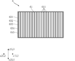
- a plurality of grooves extending in a direction perpendicular to the thickness direction of the heat dissipation layer are formed in the heat dissipation layer main surface of the heat dissipation layer.
- each of the grooves has a rectangular cross section.
- any one of the plurality of grooves is in contact with the bonding layer.
- any of the plurality of grooves is in contact with the sealing resin portion.
- a semiconductor device provided by a sixth aspect of the present invention includes a plurality of die pad portions having a die pad main surface and a die pad back surface facing in opposite directions, and a plurality of semiconductor chips mounted separately on the plurality of die pad main surfaces. And a recess that is recessed from the bottom and that exposes the back surface of each die pad in common, and is disposed in the recess, and a sealing resin portion that covers each die pad and each semiconductor chip in common, and A heat-dissipating layer main surface facing the back surface of the die pad and a heat-dissipating layer back surface opposite to the heat-dissipating layer main surface, and a heat-dissipating layer bonded in common to each of the die pad parts.
- the pair of pressing pieces of the bonding target object is pressed in a state where the pair of pressing pieces are pressed at two spaced apart positions on the bonding target object. It has a wire bonding step of bonding a wire to a portion located between the pair of pressing pieces in the direction in which the pieces are separated.
- the wire in the wire bonding step, is bonded to a portion of the bonding target that intersects a straight line connecting the pair of pressing pieces.
- the bonding object includes a die pad portion made of a metal plate, and a semiconductor chip mounted on the die pad portion and having one or more electrodes.
- a wire bonding step Then, a wire is bonded to the electrode in a state where the pair of pressing pieces are pressed at a position sandwiching the semiconductor chip in the die pad portion.
- the semiconductor chip has a plurality of electrodes, and in the wire bonding step, the pair of pressing pieces are pressed to a position sandwiching the plurality of electrodes.
- the wires are individually bonded to the plurality of electrodes.
- the bonding object includes a wire bonding portion made of a metal plate, and in the wire bonding step, the pair of pressing pieces are pressed against the wire bonding portion. Then, a wire is bonded to the wire bonding portion.
- the bonding object includes a die pad portion made of a metal plate, a semiconductor chip mounted on the die pad portion and having one or more electrodes, and a wire bonding portion separated from the die pad portion.
- a wire bonding step a wire is bonded to the electrode in a state where the pair of pressing pieces are pressed to a position where the semiconductor chip is sandwiched in the die pad portion, and the wire bonding step Thereafter, there is an additional wire bonding step of bonding a wire to the wire bonding portion in a state where an additional pair of pressing pieces are pressed against the wire bonding portion.
- the semiconductor chip has a plurality of electrodes, and in the wire bonding step, the pair of pressing pieces are pressed to a position sandwiching the plurality of electrodes.
- the wires are individually bonded to the plurality of electrodes.
- the wire is made of aluminum.
- pressure and vibration are applied to the wire in the wire bonding step.
- a semiconductor device provided by an eighth aspect of the present invention includes a die pad portion having a main surface and a back surface facing in opposite directions, and a semiconductor mounted on the main surface of the die pad portion and having one or more electrodes.
- a chip, and a sealing resin portion that covers the die pad portion and the semiconductor chip, and the die pad portion is formed with a pair of pressing marks that are spaced apart from each other, and the pair of pressing members among the electrodes.
- One end of the wire is bonded to a portion located between the pair of pressing marks in the direction in which the marks are separated.
- one end of the wire is bonded to a portion of the electrode that intersects a straight line that connects the pair of pressing marks.
- it further comprises a wire bonding portion spaced from the die pad portion, and an additional pair of pressing marks spaced from each other is formed in the wire bonding portion, The other end of the wire is bonded to a portion located between the additional pair of pressing marks in the direction in which the additional pair of pressing marks is separated from the wire bonding portion.
- the other end of the wire is bonded to a portion of the wire bonding portion that intersects a straight line connecting the additional pair of pressing marks.
- a semiconductor device provided by a ninth aspect of the present invention includes a die pad portion having a main surface and a back surface facing in opposite directions, and a semiconductor mounted on the main surface of the die pad portion and having one or more electrodes.
- a chip, a lead electrically connected to the semiconductor chip via a wire, and a sealing resin portion covering the die pad part, the semiconductor chip and a part of the lead, and the wire of the lead A pair of pressing marks that are spaced apart from each other are formed on the surface of the lead that sandwiches the connection part to which one end is bonded.
- the lead having the pressing mark has a wider portion than the lead having no pressing mark.
- the wires have different types of thickness, and the pressing marks are formed only near the connecting portion of the wire having a large thickness.
- the thick wires electrically connect only some of the semiconductor chips and the leads.
- a pair of pressing marks that are spaced apart from each other with the semiconductor chip interposed therebetween are formed on the surface of the die pad that sandwiches the semiconductor chip.
- the semiconductor chip includes a plurality of semiconductor chips and includes an output transistor and a semiconductor chip for controlling the output transistor.
- the lead pressing mark is formed on the lead connected to the output transistor. They are formed so as to be separated from each other with the connecting portion interposed therebetween.
- a method for manufacturing a semiconductor device comprising: an application step of applying a conductive bonding paste to a main surface of a die pad portion; The back surface of the semiconductor chip, which is larger than the region where the bonding paste is applied, is in contact with the conductive bonding paste so as to include the region where the conductive bonding paste is applied inward as viewed in the direction in which the main surface faces. And a bonding step of forming a conductive bonding material by softening and hardening the conductive bonding paste.
- the conductive bonding paste is a solder paste.
- the conductive bonding paste is filled in the opening.
- the back surface of the semiconductor chip has higher wettability with respect to the conductive bonding paste than the main surface of the die pad portion.
- the back surface of the semiconductor chip is made of Ag, Au, Ni or an alloy containing these metals, and the main surface of the die pad portion is any one of Cu, FeNi alloy, and Fe. It consists of *
- a semiconductor device provided by an eleventh aspect of the present invention is interposed between a die pad portion having a main surface, a semiconductor chip having a back surface, the main surface of the die pad portion and the back surface of the semiconductor chip, A conductive bonding material for bonding the die pad portion and the semiconductor chip, and a bonding area between the back surface of the semiconductor chip and the conductive bonding material is determined by the main surface of the die pad portion and the conductive material. It is characterized by being larger than the bonding area with the adhesive bonding material.
- the conductive bonding material is solder.
- the back surface of the semiconductor chip has higher wettability with respect to the conductive bonding paste than the main surface of the die pad portion.
- the back surface of the semiconductor chip is made of Ag, Au, Ni or an alloy containing these metals, and the main surface of the die pad portion is any one of Cu, FeNi alloy, and Fe. It consists of *
- a semiconductor device provided by a twelfth aspect of the present invention includes a die pad portion having a main surface and a back surface facing in opposite directions, a plurality of semiconductor chips mounted on the main surface of the die pad portion, and the die pad portion.
- a conductive bonding material that is interposed between the main surface of the semiconductor chip and the back surfaces of the plurality of semiconductor chips, and bonds the die pad portion and the plurality of semiconductor chips.
- the bonding area between each back surface and the conductive bonding material is larger than the bonding area between the conductive bonding material formed on the main surface of the die pad portion corresponding to the semiconductor chip. It is said. *
- the semiconductor chip has a plurality of output transistors and a semiconductor chip for controlling the output transistors, and the plurality of output transistors have the relationship of the junction area.
- the apparatus further includes a plurality of leads for taking out outputs of the plurality of output transistors to the outside, and a plurality of wires for connecting the output transistors and the leads, respectively. Is aluminum. *
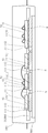
- FIG. 4 is a sectional view taken along line IV-IV in FIG. 2. It is a principal part expanded sectional view of FIG. It is a top view which shows 1 process of the manufacturing method of the semiconductor device based on 1A embodiment of this invention.
- FIG. 7 is a cross-sectional view showing a step subsequent to FIG. 6.
- FIG. 8 is a cross-sectional view showing a step subsequent to FIG. 7.
- FIG. 9 is a cross-sectional view showing a step subsequent to FIG. 8.
- It is a bottom view before bending the lead
- It is a principal part expanded sectional view which follows the XI-XI line of FIG.
- FIG. 18 is a cross-sectional view showing a step subsequent to FIG. 17.
- FIG. 19 is a cross-sectional view showing a step subsequent to FIG. 18.
- FIG. 20 is a cross-sectional view showing a step subsequent to FIG. 19.
- FIG. 22 is an essential part enlarged cross-sectional view along the line XXII-XXII in FIG. 21. It is sectional drawing which shows the mounting structure of the semiconductor device based on 1C Embodiment of this invention. It is a top view (a part of composition omitted) before bending a lead of a semiconductor device based on 1C embodiment of the present invention. It is a bottom view before bending the lead
- FIG. 25 is a sectional view taken along line XXVI-XXVI in FIG. 24.
- FIG. 29 is a cross-sectional view showing a step subsequent to FIG. 28. It is sectional drawing which shows the semiconductor device based on 2C Embodiment of this invention.
- FIG. 31 is a plan view showing a heat dissipation layer of the semiconductor device shown in FIG. 30. It is sectional drawing which shows the mounting structure of the semiconductor device based on 1D Embodiment of this invention.
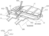
- FIG. 10 is a plan view (partially omitted) of a lead before bending a lead of a semiconductor device according to the first embodiment of the present invention; It is a principal part top view of the semiconductor device based on 1D Embodiment of this invention. It is a bottom view before bending the lead
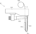
- FIG. 34 is a cross-sectional view taken along line XXXVI-XXXVI in FIG. 33. It is a top view which shows 1 process of the manufacturing method of the semiconductor device based on 1D Embodiment of this invention. It is a side view which shows an example of the bonding apparatus used for the wire bonding method which concerns on this invention.
- FIG. 43 is a perspective view of relevant parts showing one process subsequent to FIG. 42.
- FIG. 43 is a plan view of relevant parts showing one process following FIG. 42.
- FIG. 43 is a plan view showing a process following FIG. 42.
- FIG. 46 is a cross-sectional view showing a process following FIG. 45.
- FIG. 47 is a cross-sectional view showing a process following FIG. 46.
- FIG. 48 is a cross-sectional view showing a process following FIG.
- FIG. 47 It is sectional drawing which shows the mounting structure of the semiconductor device based on 1E Embodiment of this invention. It is a top view (a part of composition omitted) before bending a lead of a semiconductor device based on a 1E embodiment of the present invention. It is a bottom view before bending the lead
- FIG. 52 is a cross-sectional view taken along line LII-LII in FIG. 50. It is a principal part expanded sectional view of FIG. It is a top view which shows 1 process of the manufacturing method of the semiconductor device based on 1E Embodiment of this invention.
- FIG. 55 is an essential part enlarged cross-sectional view showing a process following FIG.
- FIG. 56 is an essential part enlarged cross-sectional view showing a process following FIG. 55.
- FIG. 57 is an essential part enlarged cross-sectional view showing a process following FIG. 56;
- FIG. 58 is an essential part enlarged cross-sectional view showing a process following FIG. 57.
- FIG. 59 is an essential part enlarged cross-sectional view showing a process following FIG. 58.
- FIG. 60 is a plan view showing a process following FIG. 59.
- FIG. 61 is a plan view showing a process following FIG. 60.
- FIG. 62 is a cross-sectional view showing a process following FIG. 61.
- FIG. 63 is a cross-sectional view showing a process following FIG. 62.
- FIG. 64 is a cross-sectional view showing a process following FIG. 63.
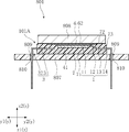
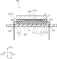
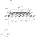
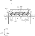
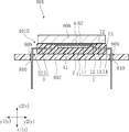
- FIG. 1 is a cross-sectional view showing a mounting structure in which a semiconductor device according to the first embodiment of the present invention is used. *
- a semiconductor device mounting structure 801 illustrated in FIG. 1 includes a semiconductor device 101A, a substrate 807, and a heat dissipation member 808. *
- the substrate 807 has a plurality of electronic components mounted thereon.
- the substrate 807 is made of an insulating material.
- a wiring pattern (not shown) is formed on the substrate 807.
- a plurality of holes 809 are formed in the substrate 807.
- the heat radiating member 808 is made of a material having a relatively large thermal conductivity, for example, a metal such as aluminum.
- the heat dissipation member 808 is fixed to the substrate 807 by a support member (not shown).
- the semiconductor device 101A is mounted on the substrate 807.
- the semiconductor device 101A is a product called IPM (Intelligent Power Module).
- the semiconductor device 101A is used for applications such as power control for air conditioners and motor control devices, for example. *
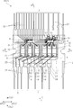
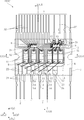
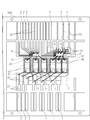
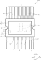
- FIG. 2 is a plan view (partially omitted) of the lead before bending the lead of the semiconductor device according to the first embodiment of the present invention.
- FIG. 3 is a bottom view of the semiconductor device according to the first embodiment of the present invention before bending the leads.
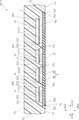
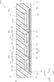
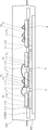
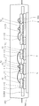
- 4 is a cross-sectional view taken along line IV-IV in FIG.
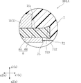
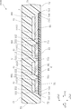
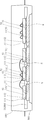
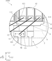
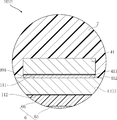
- FIG. 5 is an enlarged cross-sectional view of a main part of FIG. 1 corresponds to a cross section taken along line II in FIG. In FIG. 4, for convenience of understanding, each configuration is schematically shown. *
- the semiconductor device 101A shown in these drawings includes a plurality of first electrode portions 1, a second electrode portion 2, a third electrode portion 3, a plurality of semiconductor chips 41 and 42, a passive component chip 43, and a heat dissipation layer. 6, a sealing resin portion 7, and a wire 8.
- the heat dissipation layer 6 is indicated by a dotted line
- the sealing resin portion 7 is indicated by a virtual line.
- the sealing resin part 7 covers the first electrode part 1, the second electrode part 2, the third electrode part 3, the semiconductor chips 41 and 42, and the passive component chip 43.
- the sealing resin portion 7 is made of, for example, a black epoxy resin. As shown in FIGS. 3 and 4, the sealing resin portion 7 has a resin main surface 71, a resin bottom surface 72, and a resin side surface 73. *
- the resin main surface 71 is a flat surface that faces the direction z1 and extends along the xy plane.
- the resin bottom surface 72 is a flat surface that faces the direction z2 opposite to the direction z1 and extends along the xy plane.
- the resin side surface 73 has a shape surrounding the semiconductor chips 41 and 42 and the passive component chip 43 in the xy plan view. The resin side surface 73 is connected to the resin main surface 71 and the resin bottom surface 72.
- a recess 75 is formed in the sealing resin portion 7.
- the recess 75 is recessed from the resin bottom surface 72.
- the recess 75 has a recess bottom surface 751, a recess side surface 752, and a recess groove 753.
- the recess bottom surface 751 has a shape along the xy plane.
- the concave side surface 752 is connected to the resin bottom surface 72.
- the concave side surface 752 is generally along the direction z. *
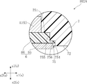
- the recess groove 753 is located between the recess bottom surface 751 and the recess side surface 752, and is arranged in a rectangular ring shape along the outer edge of the recess 75 as viewed in the z direction in this embodiment. As shown in FIG. 5, the recessed groove 753 is recessed from the recessed bottom surface 751 in the z1 direction. In the present embodiment, the recessed groove 753 is disposed outside the metal layer 65 when viewed in the z direction. Further, the concave groove 753 is inclined so as to be positioned in the z1 direction as it is separated from the concave bottom surface 751 in the x direction. The depth of the deepest portion of the recessed groove 753 is, for example, about 50 ⁇ m. *
- the semiconductor chips 41 and 42 and the passive component chip 43 have a rectangular shape in plan view.
- the semiconductor chip 41 is a power chip such as an IGBT, a MOS, or a diode, for example.
- the semiconductor chip 42 is an LSI chip such as a control IC.
- the passive component chip 43 is a passive component such as a resistor or a capacitor, for example. *
- the first electrode portion 1, the second electrode portion 2, and the third electrode portion 3 shown in FIGS. 2 to 4 are all made of a conductive material.
- An example of such a conductive material is copper. 2 is connected to the ground. *
- a plurality (four in the present embodiment) of first electrode parts 1 are respectively a die pad part 11 (see FIGS. 1, 2, and 4), a connection part 12 (see FIGS. 1 and 2), and a wire bonding part. 13 (see FIGS. 1 and 2) and a lead 14 (see FIGS. 1 to 3).
- the plurality of first electrode portions 1 are separated from each other in the direction x. *
- Each die pad portion 11 has a plate shape along the xy plane.
- a semiconductor chip 41 is disposed on the die pad portion 11.
- a bonding layer 991 is interposed between the die pad portion 11 and the semiconductor chip 41.
- the bonding layer 991 is made of a conductive material.
- a conductive material is, for example, solder or silver paste.
- Solder has a relatively high thermal conductivity. When solder is used as the bonding layer 991, heat can be efficiently transferred from the semiconductor chip 41 to the die pad portion 11. All of the plurality of die pad portions 11 are exposed from the recess bottom surface 751. *
- Each die pad portion 11 has a die pad main surface 111 and a die pad back surface 112.
- the die pad main surface 111 faces the direction z1, and the die pad back surface 112 faces the direction z2. That is, the die pad main surface 111 and the die pad back surface 112 face opposite to each other.
- a semiconductor chip 41 is arranged on the die pad main surface 111.
- a bonding layer 991 is interposed between the die pad main surface 111 and the semiconductor chip 41.
- the die pad back surface 112 is located at the same position in the thickness direction (direction z) of the die pad portion 11 with respect to the recess bottom surface 751.
- the die pad back surface 112 may be located closer to the direction in which the recess 75 opens than the recess bottom surface 751.
- each connection portion 12 is located between the die pad portion 11 and the wire bonding portion 13 and is connected to the die pad portion 11 and the wire bonding portion 13.
- the connection part 12 is a shape which follows the surface which inclines to xy plane.
- the connection portion 12 is inclined with respect to the xy plane so as to be directed in the direction z1 as it is separated from the die pad portion 11.
- Each wire bonding portion 13 shown in FIGS. 1 and 2 has a shape along the xy plane. Each wire bonding part 13 is located in the direction z1 side with respect to the die pad part 11 in the direction z.
- a wire 8 is bonded to one wire bonding portion 13 and one semiconductor chip 41. Thereby, one wire bonding part 13 and one semiconductor chip 41 are electrically connected.
- the lead 14 is connected to the wire bonding part 13. Each lead 14 extends along direction y.
- the lead 14 has a portion protruding from the resin side surface 73 of the sealing resin portion 7. In this embodiment, the lead 14 is for insertion mounting. As shown in FIG. 1, the lead 14 is bent and inserted into the hole 809 when the semiconductor device 101 ⁇ / b> A is mounted on the substrate 807. In order to fix the lead 14 to the substrate 807, the hole 809 is filled with a solder layer 810. *
- the plurality (three in this embodiment) of second electrode portions 2 each include a wire bonding portion 23 and leads 24.
- the plurality of second electrode portions 2 are separated from each other in the direction x.
- Each wire bonding portion 23 has a shape along the xy plane. Each wire bonding part 23 is located in the direction z1 side rather than the die pad part 11 in the direction z.
- a wire 8 is bonded to one wire bonding portion 23 and one semiconductor chip 41. Thereby, one wire bonding part 23 and one semiconductor chip 41 are electrically connected.
- the lead 24 is connected to the wire bonding part 23. Each lead 24 extends along direction y.
- the lead 24 has a portion protruding from the resin side surface 73 of the sealing resin portion 7. In this embodiment, the lead 24 is for insertion mounting. Although not shown, like the lead 14, the lead 24 is inserted into the hole 809 when the semiconductor device 101 ⁇ / b> A is mounted on the substrate 807. *
- the third electrode portion 3 shown in FIGS. 1 and 2 includes a plurality of control die pad portions 31 and a plurality of leads 32. Both the control die pad portion 31 and the lead 32 are arranged at the same position in the direction z. In each control die pad portion 31, a semiconductor chip 42 or a passive component chip 43 is arranged. A bonding layer (not shown) is interposed between the control die pad portion 31 and the semiconductor chip 42 and between the control die pad portion 31 and the passive component chip 43. The back surface of the control die pad portion 31 may not face the heat dissipation layer 6 or may not be exposed. *
- Each lead 32 has a portion protruding from the resin side surface 73 of the sealing resin portion 7.
- the lead 32 is for insertion mounting.
- the lead 32 is inserted into the hole 809 when the semiconductor device 101 ⁇ / b> A is mounted on the substrate 807.
- the hole 809 is filled with a solder layer 810 to secure the lead 32 to the substrate 807.
- a wire 8 is bonded to one lead 32 and one semiconductor chip 42.
- one lead 32 and one semiconductor chip 42 are electrically connected.
- the wire 8 is also bonded to one semiconductor chip 42 and one passive component chip 43. *
- the heat dissipation layer 6 is disposed in the recess 75 in the sealing resin portion 7.
- the heat dissipation layer 6 is surrounded by the concave side surface 752.
- the heat dissipation layer 6 has a plate shape along the xy plane.
- the heat dissipation layer 6 includes a metal layer 65 and a bonding layer 66.
- the metal layer 65 is on the z2 direction side and is made of, for example, Cu, aluminum, or ceramics having a thickness of about 105 ⁇ m.
- the bonding layer 66 is on the z1 direction side with respect to the metal layer 65 and functions to bond the metal layer 65 to the die pad back surfaces 112 of the plurality of die pad portions 11.
- the bonding layer 66 is made of, for example, an insulating resin and has a thickness of about 250 ⁇ m, for example. This resin is a material that softens when pressure and vibration are applied in the manufacturing process of the semiconductor device 101A.
- the bonding layer 66 is in direct contact with any of the plurality of die pad portions 11 on which the semiconductor chip 41 is mounted.
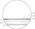
- the metal layer 65 may have a portion that slightly protrudes from the resin bottom surface 72. As shown in FIG. 5, a part of the bonding layer 66 fills the concave groove 753. Further, the bonding layer 66 is in contact with the concave side surface 752. *
- the heat dissipation layer 6 is provided to quickly release the heat generated in the semiconductor chip 41 to the outside of the semiconductor device 101A.
- the heat radiation layer 6 is made of a material having a thermal conductivity larger than that of the material constituting the sealing resin portion 7 and a thermal expansion coefficient close to that of the sealing resin portion 7.
- the heat dissipation layer 6 faces all of the plurality of die pad portions 11. As shown in FIG. 3, the heat dissipation layer 6 overlaps the entirety of each die pad portion 11 in the xy plan view (view in the thickness direction of the heat dissipation layer 6). *
- the heat dissipation layer 6 has a heat dissipation layer main surface 61 and a heat dissipation layer back surface 62.
- the heat radiation layer main surface 61 faces the direction z1.
- the heat radiation layer main surface 61 overlaps the die pad back surface 112 of each die pad portion 11 and the recess bottom surface 751 in the xy plan view.
- the heat radiation layer main surface 61 is in direct contact with the die pad back surface 112 and the recess bottom surface 751.
- the heat radiation layer back surface 62 faces in the direction z ⁇ b> 2, which is the opposite direction to the direction in which the heat radiation layer main surface 61 faces.
- the heat radiation layer back surface 62 is not covered with the sealing resin portion 7 and is exposed from the sealing resin portion 7. *
- a lead frame 300 including a plurality of die pad portions 11 and 31, a plurality of semiconductor chips 41 and 42, and a passive component chip 43 are prepared.
- each semiconductor chip 41 is arranged on any one of the plurality of die pad portions 11 via a bonding layer (not shown).
- each semiconductor chip 42 and the passive component chip 43 are arranged on any one of the plurality of control die pad portions 31 via a bonding layer (not shown).
- the wire 8 is bonded to each of the semiconductor chips 41, 42 and the like.
- a sealing resin portion 7 is formed.
- the sealing resin portion 7 is formed by molding using a mold 881.
- a plurality of die pad portions 11 and the like are pressed with a mold 881.
- a resin material is injected into the mold 881 to cure the resin material.
- the mold 881 is removed from the plurality of die pad portions 11 and the like as shown in FIG. Thereby, the sealing resin part 7 can be formed.
- the concave portions 75 that expose the plurality of die pad portions 11 are formed in the sealing resin portion 7. *
- the heat dissipation layer 6 is fitted into the recess 75 of the sealing resin portion 7. Then, pressure and vibration are applied to the heat dissipation layer 6. Further, the heat dissipation layer 6 may be heated. By the pressurization, vibration, and heating, the bonding layer 66 of the heat dissipation layer 6 is softened. The softened bonding layer 66 moves in the recess 75, and a part thereof is filled in the recess groove 753. Further, the bonding layer 66 is in contact with the concave side surface 752. *
- the lead frame 300 shown in FIG. 6 is appropriately cut to manufacture the semiconductor device 101A shown in FIG. *
- the bonding layer 66 fills the concave groove 753.
- the bonding layer 66 can be prevented from overflowing from the recess 75 by the amount of filling. Therefore, it is possible to prevent the gap between the heat dissipation layer 6 and the heat dissipation member 808 due to the bonding layer 66 overflowing outside the metal layer 65, and efficiently dissipate heat from the semiconductor chips 41 and 42. can do.
- the concave groove 753 By forming the concave groove 753 into a tapered shape, even if the position of the metal layer 65 in the x direction or the y direction is shifted, the volume of the concave groove 753 overlapping the metal layer 65 in the z direction can be reduced. This is preferable for eliminating the above-mentioned voids.
- the recess 75 includes a plurality of recess grooves 753, and further includes a plurality of recess first side surfaces 754, a recess second side surface 755, and a recess support surface 756.
- a plurality of recess grooves 753 and a plurality of recess first side surfaces 754, recess second side surfaces 755, and recess support surfaces 756 are alternately arranged along the outer edge of the recess 75.
- a recess first side surface 754, a recess second side surface 755, and a recess support surface 756 are disposed. *
- the concave first side surface 754 is connected to the resin bottom surface 72 and is generally along the z direction.
- the concave first side surface 754 is located outside the die pad portion 11 when viewed in the z direction.
- the concave second side surface 755 is connected to the concave bottom surface 751 and is generally along the z direction.
- the concave second side surface 755 is located between the die pad portion 11 and the concave first side surface 754 when viewed in the z direction.
- the recessed portion support surface 756 connects the recessed portion first side surface 754 and the recessed portion second side surface 755 and generally faces the z2 direction.
- the region surrounded by the concave second side surface 755 is filled with the bonding layer 66.
- a part of the bonding layer 66 is interposed between the metal layer 65 and the concave support surface 756.
- the metal layer 65 is at least indirectly supported by the concave support surface 756. For this reason, it is possible to prevent the metal layer 65 from being unduly inclined or recessed with respect to the resin bottom surface 72. Therefore, it is possible to suppress a gap from being formed between the heat dissipation member 808 attached so as to be in close contact with the metal layer 65, and heat dissipation from the semiconductor chips 41 and 42 can be enhanced.
- the metal layer 65 can be reliably fixed to the sealing resin portion 7. If the bonding layer 66 does not reach the end of the metal layer 65, the peeling of the metal layer 65 may propagate from that portion. In this embodiment, there is little such a possibility.
- the present invention is not limited to the embodiment described above.
- the specific configuration of each part of the present invention can be changed in various ways. For example, if it is a semiconductor device in which the metal layer is exposed from the back surface of the sealing resin, it can be similarly used in the case of a terminal for surface mounting instead of insertion mounting.
- the present invention can also be applied to a semiconductor device that seals a drive element that has only one semiconductor chip and one island and the metal layer is exposed from the back surface of the sealing resin.
- FIG. 12 is a cross-sectional view showing a mounting structure in which the semiconductor device according to the first embodiment of the present invention is used. *
- a semiconductor device mounting structure 801 illustrated in FIG. 12 includes a semiconductor device 101B, a substrate 807, and a heat dissipation member 808. *
- the substrate 807 has a plurality of electronic components mounted thereon.
- the substrate 807 is made of an insulating material.
- a wiring pattern (not shown) is formed on the substrate 807.
- a plurality of holes 809 are formed in the substrate 807.
- the heat radiating member 808 is made of a material having a relatively large thermal conductivity, for example, a metal such as aluminum.
- the heat dissipation member 808 is fixed to the substrate 807 by a support member (not shown).
- the semiconductor device 101B is mounted on the substrate 807.
- the semiconductor device 101B is a product called IPM (Intelligent Power Module).
- the semiconductor device 101B is used for applications such as power control for air conditioners and motor control devices, for example. *
- FIG. 13 is a plan view (partially omitted) of a lead before bending a lead of the semiconductor device according to the first embodiment of the present invention.
- FIG. 14 is a bottom view of the semiconductor device according to the first embodiment of the present invention before bending the leads.
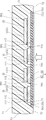
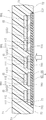
- FIG. 15 is a sectional view taken along line XV-XV in FIG. 16 is an enlarged cross-sectional view of a main part of FIG. 12 corresponds to a cross section taken along line XII-XII in FIG. In FIG. 15, for convenience of understanding, each configuration is schematically shown.
- the semiconductor device 101B shown in these drawings includes a plurality of first electrode portions 1, a second electrode portion 2, a third electrode portion 3, a plurality of semiconductor chips 41 and 42, a passive component chip 43, and a heat dissipation layer. 6, a sealing resin portion 7, and a wire 8.
- the heat radiation layer 6 is indicated by a dotted line
- the sealing resin portion 7 is indicated by a virtual line. *
- the sealing resin part 7 covers the first electrode part 1, the second electrode part 2, the third electrode part 3, the semiconductor chips 41 and 42, and the passive component chip 43.
- the sealing resin portion 7 is made of, for example, a black epoxy resin. As shown in FIGS. 14 and 15, the sealing resin portion 7 has a resin main surface 71, a resin bottom surface 72, and a resin side surface 73. *
- the resin main surface 71 is a flat surface that faces the direction z1 and extends along the xy plane.
- the resin bottom surface 72 is a flat surface that faces the direction z2 opposite to the direction z1 and extends along the xy plane.
- the resin side surface 73 has a shape surrounding the semiconductor chips 41 and 42 and the passive component chip 43 in the xy plan view. The resin side surface 73 is connected to the resin main surface 71 and the resin bottom surface 72.
- a recess 75 is formed in the sealing resin portion 7.
- the recess 75 is recessed from the resin bottom surface 72.
- the recess 75 has a recess bottom surface 751, a recess first side surface 754, a recess second side surface 755, and a recess support surface 756.
- the recess bottom surface 751 has a shape along the xy plane.
- the concave side surface 752 is connected to the resin bottom surface 72. *
- the concave first side surface 754 is connected to the resin bottom surface 72 and is generally along the z direction.
- the concave first side surface 754 is located outside the die pad portion 11 when viewed in the z direction.
- the concave second side surface 755 is connected to the concave bottom surface 751 and is generally along the z direction.
- the concave second side surface 755 is located between the die pad portion 11 and the concave first side surface 754 when viewed in the z direction.
- the recessed portion support surface 756 connects the recessed portion first side surface 754 and the recessed portion second side surface 755 and generally faces the z2 direction.
- the semiconductor chips 41 and 42 and the passive component chip 43 have a rectangular shape in plan view.
- the semiconductor chip 41 is a power chip such as an IGBT, a MOS, or a diode, for example.
- the semiconductor chip 42 is an LSI chip such as a control IC.
- the passive component chip 43 is a passive component such as a resistor or a capacitor, for example. *
- the first electrode part 1, the second electrode part 2, and the third electrode part 3 shown in FIGS. 13 to 4 are all made of a conductive material.
- An example of such a conductive material is copper. Note that the electrode portion shown in the lower right of FIG. 13 is grounded. *
- the plurality of (four in this embodiment) first electrode portions 1 are respectively a die pad portion 11 (see FIGS. 12, 13, and 15), a connection portion 12 (see FIGS. 12 and 13), and a wire bonding portion. 13 (see FIGS. 12 and 13) and a lead 14 (see FIGS. 12 to 14).
- the plurality of first electrode portions 1 are separated from each other in the direction x. *
- Each die pad portion 11 has a plate shape along the xy plane.
- a semiconductor chip 41 is disposed on the die pad portion 11.
- a bonding layer 991 is interposed between the die pad portion 11 and the semiconductor chip 41.
- the bonding layer 991 is made of a conductive material.
- a conductive material is, for example, solder or silver paste.
- Solder has a relatively high thermal conductivity. When solder is used as the bonding layer 991, heat can be efficiently transferred from the semiconductor chip 41 to the die pad portion 11. All of the plurality of die pad portions 11 are exposed from the recess bottom surface 751. *
- Each die pad portion 11 has a die pad main surface 111 and a die pad back surface 112.
- the die pad main surface 111 faces the direction z1, and the die pad back surface 112 faces the direction z2. That is, the die pad main surface 111 and the die pad back surface 112 face opposite to each other.
- a semiconductor chip 41 is arranged on the die pad main surface 111.
- a bonding layer 991 is interposed between the die pad main surface 111 and the semiconductor chip 41.
- the die pad back surface 112 is located at the same position in the thickness direction (direction z) of the die pad portion 11 with respect to the recess bottom surface 751.
- the die pad back surface 112 may be located closer to the direction in which the recess 75 opens than the recess bottom surface 751.
- each connection portion 12 is located between the die pad portion 11 and the wire bonding portion 13 and is connected to the die pad portion 11 and the wire bonding portion 13.
- the connection part 12 is a shape along the surface which inclines to xy plane.
- the connection portion 12 is inclined with respect to the xy plane so as to be directed in the direction z1 as it is separated from the die pad portion 11.
- Each wire bonding portion 13 shown in FIGS. 12 and 13 has a shape along the xy plane. Each wire bonding part 13 is located in the direction z1 side with respect to the die pad part 11 in the direction z.
- a wire 8 is bonded to one wire bonding portion 13 and one semiconductor chip 41. Thereby, one wire bonding part 13 and one semiconductor chip 41 are electrically connected.
- the lead 14 is connected to the wire bonding part 13. Each lead 14 extends along direction y.
- the lead 14 has a portion protruding from the resin side surface 73 of the sealing resin portion 7. In this embodiment, the lead 14 is for insertion mounting. As shown in FIG. 12, the lead 14 is bent and inserted into the hole 809 when the semiconductor device 101 ⁇ / b> B is mounted on the substrate 807. In order to fix the lead 14 to the substrate 807, the hole 809 is filled with a solder layer 810. *
- the plurality (three in this embodiment) of second electrode portions 2 each include a wire bonding portion 23 and leads 24.
- the plurality of second electrode portions 2 are separated from each other in the direction x. *
- Each wire bonding portion 23 has a shape along the xy plane. Each wire bonding part 23 is located in the direction z1 side rather than the die pad part 11 in the direction z.
- a wire 8 is bonded to one wire bonding portion 23 and one semiconductor chip 41. Thereby, one wire bonding part 23 and one semiconductor chip 41 are electrically connected.
- the lead 24 is connected to the wire bonding part 23. Each lead 24 extends along direction y.
- the lead 24 has a portion protruding from the resin side surface 73 of the sealing resin portion 7. In this embodiment, the lead 24 is for insertion mounting. Although not shown, like the lead 14, the lead 24 is inserted into the hole 809 when the semiconductor device 101 ⁇ / b> B is mounted on the substrate 807. *
- the third electrode unit 3 shown in FIGS. 12 and 13 includes a plurality of control die pad units 31 and a plurality of leads 32. Both the control die pad portion 31 and the lead 32 are arranged at the same position in the direction z. In each control die pad portion 31, a semiconductor chip 42 or a passive component chip 43 is arranged. A bonding layer (not shown) is interposed between the control die pad portion 31 and the semiconductor chip 42 and between the control die pad portion 31 and the passive component chip 43. The back surface of the control die pad portion 31 may not face the heat dissipation layer 6 or may not be exposed. *
- Each lead 32 has a portion protruding from the resin side surface 73 of the sealing resin portion 7.
- the lead 32 is for insertion mounting.
- the lead 32 is inserted into the hole 809 when the semiconductor device 101 ⁇ / b> B is mounted on the substrate 807.
- the hole 809 is filled with a solder layer 810 to secure the lead 32 to the substrate 807.
- a wire 8 is bonded to one lead 32 and one semiconductor chip 42. Thereby, one lead 32 and one semiconductor chip 42 are electrically connected.
- the wire 8 is also bonded to one semiconductor chip 42 and one passive component chip 43. *
- the heat dissipation layer 6 is disposed in the recess 75 in the sealing resin portion 7.
- the heat dissipation layer 6 is surrounded by the concave first side surface 754 and the concave second side surface 755.
- the heat dissipation layer 6 has a plate shape along the xy plane.
- the heat dissipation layer 6 includes a metal layer 65 and a bonding layer 66.
- the metal layer 65 is on the z2 direction side and is made of, for example, Cu, aluminum, or ceramics having a thickness of about 105 ⁇ m.
- the metal layer 65 corresponds to an example of the heat dissipation layer in the present invention.
- the bonding layer 66 is on the z1 direction side with respect to the metal layer 65 and functions to bond the metal layer 65 to the die pad back surfaces 112 of the plurality of die pad portions 11.
- the bonding layer 66 is made of, for example, an insulating resin and has a thickness of about 250 ⁇ m, for example. This resin is a material that softens when pressure and vibration are applied in the manufacturing process of the semiconductor device 101B.
- the bonding layer 66 is in direct contact with any of the plurality of die pad portions 11 on which the semiconductor chip 41 is mounted.
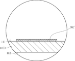
- the metal layer 65 may have a portion that slightly protrudes from the resin bottom surface 72. As shown in FIG. 16, a part of the bonding layer 66 fills a region surrounded by the concave second side surface 755. In the present embodiment, a part of the bonding layer 66 is interposed between the concave support surface 756 and the metal layer 65. *
- the heat dissipation layer 6 is provided in order to quickly release the heat generated in the semiconductor chip 41 to the outside of the semiconductor device 101B.
- the heat radiation layer 6 is made of a material having a thermal conductivity larger than that of the material constituting the sealing resin portion 7 and a thermal expansion coefficient close to that of the sealing resin portion 7.
- the heat dissipation layer 6 faces all of the plurality of die pad portions 11. As shown in FIG. 14, the heat radiation layer 6 overlaps the entirety of each die pad portion 11 in the xy plan view (view in the thickness direction of the heat radiation layer 6). *
- the heat dissipation layer 6 has a heat dissipation layer main surface 61 and a heat dissipation layer back surface 62.
- the heat radiation layer main surface 61 faces the direction z1.
- the heat radiation layer main surface 61 overlaps the die pad back surface 112 of each die pad portion 11 and the recess bottom surface 751 in the xy plan view.
- the heat radiation layer main surface 61 is in direct contact with the die pad back surface 112 and the recess bottom surface 751.
- the heat radiation layer back surface 62 faces in the direction z ⁇ b> 2, which is the opposite direction to the direction in which the heat radiation layer main surface 61 faces.
- the heat radiation layer back surface 62 is not covered with the sealing resin portion 7 and is exposed from the sealing resin portion 7. *
- a lead frame 300 including a plurality of die pad portions 11 and 31, a plurality of semiconductor chips 41 and 42, and a passive component chip 43 are prepared.
- each semiconductor chip 41 is arranged on any one of the plurality of die pad portions 11 via a bonding layer (not shown).
- each semiconductor chip 42 and the passive component chip 43 are arranged on any one of the plurality of control die pad portions 31 via a bonding layer (not shown).
- the wire 8 is bonded to each of the semiconductor chips 41, 42 and the like.
- the sealing resin portion 7 is formed.
- the sealing resin portion 7 is formed by molding using a mold 881.
- a plurality of die pad portions 11 and the like are pressed with a mold 881.
- a resin material is injected into the mold 881 to cure the resin material.
- the mold 881 is removed from the plurality of die pad portions 11 and the like as shown in FIG. Thereby, the sealing resin part 7 can be formed.
- the concave portions 75 that expose the plurality of die pad portions 11 are formed in the sealing resin portion 7. *
- the heat dissipation layer 6 is fitted into the recess 75 of the sealing resin portion 7. Then, pressure and vibration are applied to the heat dissipation layer 6. Further, the heat dissipation layer 6 may be heated. By the pressurization, vibration, and heating, the bonding layer 66 of the heat dissipation layer 6 is softened. The softened bonding layer 66 moves in the recess 75, and a part thereof is filled in the region surrounded by the recess second side surface 755. A part of the bonding layer 66 enters between the concave support surface 756 and the metal layer 65.
- the lead frame 300 shown in FIG. 17 is appropriately cut to manufacture the semiconductor device 101B shown in FIG. *
- the metal layer 65 is at least indirectly supported by the concave support surface 756. For this reason, it is possible to prevent the metal layer 65 from being unduly inclined or recessed with respect to the resin bottom surface 72. Therefore, it is possible to suppress the gap between the metal layer 65 and the heat dissipation member 808 due to the bonding layer 66 overflowing outside the metal layer 65, and to increase heat dissipation from the semiconductor chips 41 and 42, and Further, peeling of the metal layer 65 can be made difficult to occur.
- the metal layer 65 can be reliably fixed to the sealing resin portion 7. If the bonding layer 66 does not reach the end of the metal layer 65, the peeling of the metal layer 65 may propagate from that portion. In this embodiment, there is little such a possibility.
- 21 and 22 show a semiconductor device according to the second embodiment of the present invention.
- the same or similar elements as those in the above embodiment are denoted by the same reference numerals as those in the above embodiment.
- the configuration of the recess 75 is different from that of the semiconductor device 101B described above. *
- the recess 75 has a plurality of recess first side surfaces 754, a recess second side surface 755, and a recess support surface 756, and further includes a plurality of recess side surfaces 752 and a recess groove 753. ing. As shown in FIG. 21, the plurality of recess grooves 753 and the plurality of recess first side surfaces 754, the recess second side surfaces 755, and the recess support surfaces 756 are alternately arranged along the outer edge of the recess 75. In a portion corresponding to the four corners of the recess 75, a recess first side surface 754, a recess second side surface 755, and a recess support surface 756 are disposed. *
- the recess groove 753 is located between the recess bottom surface 751 and the recess side surface 752.
- the recess groove 753 is arranged in a rectangular ring shape along the outer edge of the recess 75 when viewed in the z direction. Yes.
- the recessed groove 753 is recessed from the recessed bottom surface 751 in the z1 direction.
- the concave groove 753 is inclined so as to be positioned in the z1 direction as it is separated from the concave bottom surface 751 in the x direction.
- the depth of the deepest portion of the recessed groove 753 is, for example, about 50 ⁇ m. *
- a part of the bonding layer 66 fills the concave groove 753. Further, the bonding layer 66 is in contact with the concave side surface 752.
- the bonding layer 66 fills the concave groove 753.
- the bonding layer 66 can be prevented from overflowing from the recess 75 in the manufacturing process of the semiconductor device 101B. Therefore, it is possible to prevent a gap from being formed between the heat dissipation member 808 attached so as to be in close contact with the heat dissipation layer 6, and heat from the semiconductor chips 41 and 42 can be efficiently dissipated.
- the concave groove 753 By forming the concave groove 753 into a tapered shape, even if the position of the metal layer 65 in the x direction or the y direction is shifted, the volume of the concave groove 753 overlapping the metal layer 65 in the z direction can be reduced. This is preferable for eliminating the above-mentioned voids.
- the present invention is not limited to the embodiment described above.
- the specific configuration of each part of the present invention can be changed in various ways. For example, if it is a semiconductor device in which the metal layer is exposed from the back surface of the sealing resin, it can be similarly used in the case of a terminal for surface mounting instead of insertion mounting.
- the present invention can also be applied to a semiconductor device that seals a drive element that has only one semiconductor chip and one island and the metal layer is exposed from the back surface of the sealing resin.
- a die pad portion having a main surface and a back surface facing in opposite directions, a semiconductor chip mounted on the main surface of the die pad portion, and recessed from the resin bottom surface and exposing the back surface of the die pad portion
- a recess is formed, and includes a sealing resin portion that covers the die pad portion and the semiconductor chip, and a heat dissipation layer disposed in the recess, and the recess is more than the die pad portion in the direction in which the back surface expands.
- a semiconductor device comprising: [Appendix 2] The semiconductor device according to Appendix 1, wherein the heat dissipation layer is made of metal. [Appendix 3] The semiconductor device according to Appendix 2, wherein the metal is Cu. [Appendix 4] The semiconductor device according to Appendix 2 or 3, wherein the bonding layer is made of a resin. [Appendix 5] The semiconductor device according to Appendix 4, wherein a part of the bonding layer is interposed between the support surface and the heat dissipation layer.
- the concave portion has a groove that is located outside the die pad portion in the direction in which the back surface expands and has a portion located on the main surface side from the back surface, and the bonding layer.
- Appendix 7 The semiconductor device according to Appendix 6, wherein a part of the heat dissipation layer protrudes from the recess in the thickness direction.
- Appendix 8 The semiconductor device according to Appendix 6 or 7, wherein the groove is located outside the heat dissipation layer in a direction in which the back surface expands.
- a plurality of die pad portions having a main surface and a back surface facing in opposite directions, a plurality of semiconductor chips separately mounted on the main surface of the plurality of die pad portions, and recessed from the resin bottom surface
- a recess that exposes at least a part of each back surface of the die pad portion is formed in common
- a sealing resin portion that covers each die pad portion and each semiconductor chip in common, and heat dissipation disposed in the recess A recess, and the concave portion is located outside the die pad portion on the back surface side, is connected to the resin bottom surface, is connected to the first side surface, and is a support surface that faces the back surface.
- a second side surface connected to the support surface and positioned between the die pad portion and the first side surface in a direction in which the back surface is widened.
- a heat-dissipating layer having an outer edge located at least partially between the first side surface and the second side surface in the direction in which the back surface extends, and overlapping the first side surface in the thickness direction of the die pad portion;
- a semiconductor device comprising: a bonding layer interposed between the layer and each of the die pad portions.
- FIG. 23 is a cross-sectional view showing a mounting structure in which the semiconductor device according to the first embodiment of the present invention is used. *
- a semiconductor device mounting structure 801 illustrated in FIG. 23 includes a semiconductor device 101C, a substrate 807, and a heat dissipation member 808. *
- the substrate 807 has a plurality of electronic components mounted thereon.
- the substrate 807 is made of an insulating material.
- a wiring pattern (not shown) is formed on the substrate 807.
- a plurality of holes 809 are formed in the substrate 807.
- the heat radiating member 808 is made of a material having a relatively large thermal conductivity, for example, a metal such as aluminum.
- the heat dissipation member 808 is fixed to the substrate 807 by a support member (not shown).
- the semiconductor device 101C is mounted on the substrate 807.
- the semiconductor device 101C is a product called IPM (Intelligent Power Module).
- the semiconductor device 101C is used for applications such as power control for air conditioners and motor control devices, for example. *
- FIG. 24 is a plan view (partially omitted) of the lead before bending the lead of the semiconductor device according to the first embodiment of the present invention.
- FIG. 25 is a bottom view of the semiconductor device according to the first embodiment of the present invention before bending the leads.
- 26 is a cross-sectional view taken along the line IIVI-IIVI of FIG.
- FIG. 27 is an enlarged cross-sectional view of a main part of FIG.
- FIG. 23 corresponds to a cross section taken along line XXIII-XXIII in FIG.
- each configuration is schematically shown for the sake of easy understanding. *
- the semiconductor device 101C shown in these drawings includes a plurality of first electrode parts 1, a second electrode part 2, a third electrode part 3, a plurality of semiconductor chips 41 and 42, a passive component chip 43, and a heat dissipation layer. 6, a sealing resin portion 7, and a wire 8.
- the heat radiation layer 6 is indicated by a dotted line
- the sealing resin portion 7 is indicated by a virtual line. *
- the sealing resin part 7 covers the first electrode part 1, the second electrode part 2, the third electrode part 3, the semiconductor chips 41 and 42, and the passive component chip 43.
- the sealing resin portion 7 is made of, for example, a black epoxy resin. As shown in FIGS. 25 and 26, the sealing resin portion 7 has a resin main surface 71, a resin bottom surface 72, and a resin side surface 73. *
- the resin main surface 71 is a flat surface that faces the direction z1 and extends along the xy plane.
- the resin bottom surface 72 is a flat surface that faces the direction z2 opposite to the direction z1 and extends along the xy plane.
- the resin side surface 73 has a shape surrounding the semiconductor chips 41 and 42 and the passive component chip 43 in the xy plan view. The resin side surface 73 is connected to the resin main surface 71 and the resin bottom surface 72.
- a recess 75 is formed in the sealing resin portion 7.
- the recess 75 is recessed from the resin bottom surface 72.
- the recess 75 has a recess bottom surface 751.
- the recess bottom surface 751 has a shape along the xy plane. *
- the semiconductor chips 41 and 42 and the passive component chip 43 have a rectangular shape in plan view.
- the semiconductor chip 41 is a power chip such as an IGBT, a MOS, or a diode, for example.
- the semiconductor chip 42 is an LSI chip such as a control IC.
- the passive component chip 43 is a passive component such as a resistor or a capacitor, for example. *
- the first electrode part 1, the second electrode part 2, and the third electrode part 3 shown in FIGS. 24 to 4 are all made of a conductive material.
- An example of such a conductive material is copper. Note that the electrode portion shown in the lower right of FIG. 24 is grounded. *
- a plurality (four in this embodiment) of first electrode portions 1 are respectively a die pad portion 11 (see FIGS. 23, 24, and 26), a connection portion 12 (see FIGS. 23 and 24), and a wire bonding portion. 13 (see FIGS. 23 and 24) and a lead 14 (see FIGS. 23 to 25).
- the plurality of first electrode portions 1 are separated from each other in the direction x. *
- Each die pad portion 11 has a plate shape along the xy plane.
- a semiconductor chip 41 is disposed on the die pad portion 11.
- a bonding layer 991 is interposed between the die pad portion 11 and the semiconductor chip 41.
- the bonding layer 991 is made of a conductive material.
- a conductive material is, for example, solder or silver paste.
- Solder has a relatively high thermal conductivity. When solder is used as the bonding layer 991, heat can be efficiently transferred from the semiconductor chip 41 to the die pad portion 11. All of the plurality of die pad portions 11 are exposed from the recess bottom surface 751.
- Each die pad portion 11 has a die pad main surface 111 and a die pad back surface 112.
- the die pad main surface 111 faces the direction z1, and the die pad back surface 112 faces the direction z2. That is, the die pad main surface 111 and the die pad back surface 112 face opposite to each other.
- a semiconductor chip 41 is arranged on the die pad main surface 111.
- a bonding layer 991 is interposed between the die pad main surface 111 and the semiconductor chip 41.
- the die pad back surface 112 is located at the same position in the thickness direction (direction z) of the die pad portion 11 with respect to the recess bottom surface 751.
- the die pad back surface 112 may be located closer to the direction in which the recess 75 opens than the recess bottom surface 751.
- each connection portion 12 is located between the die pad portion 11 and the wire bonding portion 13 and is connected to the die pad portion 11 and the wire bonding portion 13.
- the connecting portion 12 has a shape along a surface inclined to the xy plane.
- the connection portion 12 is inclined with respect to the xy plane so as to be directed in the direction z1 as it is separated from the die pad portion 11.
- Each wire bonding portion 13 shown in FIGS. 23 and 24 has a shape along the xy plane. Each wire bonding part 13 is located in the direction z1 side with respect to the die pad part 11 in the direction z.
- a wire 8 is bonded to one wire bonding portion 13 and one semiconductor chip 41. Thereby, one wire bonding part 13 and one semiconductor chip 41 are electrically connected.
- the lead 14 is connected to the wire bonding part 13. Each lead 14 extends along direction y.
- the lead 14 has a portion protruding from the resin side surface 73 of the sealing resin portion 7. In this embodiment, the lead 14 is for insertion mounting. As shown in FIG. 23, when the semiconductor device 101C is mounted on the substrate 807, the lead 14 is bent and inserted into the hole 809. In order to fix the lead 14 to the substrate 807, the hole 809 is filled with a solder layer 810. *
- the plurality of (three in this embodiment) second electrode portions 2 each include a wire bonding portion 23 and a lead 24.
- the plurality of second electrode portions 2 are separated from each other in the direction x. *
- Each wire bonding portion 23 has a shape along the xy plane. Each wire bonding part 23 is located in the direction z1 side rather than the die pad part 11 in the direction z.
- a wire 8 is bonded to one wire bonding portion 23 and one semiconductor chip 41. Thereby, one wire bonding part 23 and one semiconductor chip 41 are electrically connected.
- the lead 24 is connected to the wire bonding part 23. Each lead 24 extends along direction y.
- the lead 24 has a portion protruding from the resin side surface 73 of the sealing resin portion 7. In this embodiment, the lead 24 is for insertion mounting. Although not shown, like the lead 14, the lead 24 is inserted into the hole 809 when the semiconductor device 101 ⁇ / b> C is mounted on the substrate 807. *
- the third electrode unit 3 shown in FIGS. 23 and 24 includes a plurality of control die pad units 31 and a plurality of leads 32. Both the control die pad portion 31 and the lead 32 are arranged at the same position in the direction z. In each control die pad portion 31, a semiconductor chip 42 or a passive component chip 43 is arranged. A bonding layer (not shown) is interposed between the control die pad portion 31 and the semiconductor chip 42 and between the control die pad portion 31 and the passive component chip 43. The back surface of the control die pad portion 31 may not face the heat dissipation layer 6 or may not be exposed. *
- Each lead 32 has a portion protruding from the resin side surface 73 of the sealing resin portion 7.
- the lead 32 is for insertion mounting.
- the lead 32 is inserted into the hole 809 when the semiconductor device 101C is mounted on the substrate 807.
- the hole 809 is filled with a solder layer 810 to secure the lead 32 to the substrate 807.
- a wire 8 is bonded to one lead 32 and one semiconductor chip 42.
- one lead 32 and one semiconductor chip 42 are electrically connected.
- the wire 8 is also bonded to one semiconductor chip 42 and one passive component chip 43.
- the wires connected to the control semiconductor chip 42 and the passive component chip 43 are made of fine aluminum and gold wires that are thinner and softer than the wires 8. *
- the heat dissipation layer 6 is disposed in the recess 75 in the sealing resin portion 7.
- the heat dissipation layer 6 has a plate shape along the xy plane.
- the heat dissipation layer 6 is made of ceramics, Cu, or aluminum.
- the heat dissipation layer 6 has a heat dissipation layer main surface 61, a heat dissipation layer back surface 62, a first side surface 631, an intermediate surface 632, and a second side surface 633. *
- the heat radiation layer main surface 61 faces the direction z1.
- the heat radiation layer main surface 61 overlaps the die pad back surface 112 of each die pad portion 11 and the recess bottom surface 751 in the xy plan view.
- the heat radiation layer back surface 62 faces in the direction z ⁇ b> 2, which is the opposite direction to the direction in which the heat radiation layer main surface 61 faces.
- the heat radiation layer back surface 62 is not covered with the sealing resin portion 7 and is exposed from the sealing resin portion 7.
- the heat radiation layer main surface 61 of the heat radiation layer 6 is bonded to the die pad back surfaces 112 of the plurality of die pad portions 11 by the bonding layer 69.
- the bonding layer 69 is made of resin, for example. *
- the first side surface 631 is connected to the heat radiation layer back surface 62 and is generally along the z direction.
- the first side surface 631 is located outside the die pad portion 11 when viewed in the z direction.
- the second side surface 633 is connected to the heat radiation layer main surface 61 and is generally along the z direction.
- the second side surface 633 is located between the die pad portion 11 and the first side surface 631 when viewed in the z direction.
- the intermediate surface 632 connects the first side surface 631 and the second side surface 633, and generally faces the z2 direction.
- the z-direction dimension of the first side surface 631 is preferably larger than the z-direction dimension of the second side surface 633.
- the first side surface 631, the intermediate surface 632, and the second side surface 633 are all in contact with the sealing resin portion 7. Further, the heat radiation layer back surface 62 is flush with the resin bottom surface 72 of the sealing resin portion 7. As shown in FIG. 27, the first side surface 631 and the intermediate surface 632 constitute a first corner portion 634. The intermediate surface 632 and the second side surface 633 constitute a second corner portion 645. In the present embodiment, each of the first corner portion 634 and the second corner portion 645 is a right angle, but may be chamfered. *
- the heat dissipation layer 6 is provided to quickly release the heat generated in the semiconductor chip 41 to the outside of the semiconductor device 101C.
- the thermal expansion coefficient is significantly different from that of the sealing resin portion 7, there arises a problem that the heat radiation layer 6 is easily peeled off. There is a fear.
- the heat radiation layer 6 is made of a material having a thermal conductivity larger than that of the material constituting the sealing resin portion 7 and a thermal expansion coefficient close to that of the sealing resin portion 7.
- the heat dissipation layer 6 faces all of the plurality of die pad portions 11. As shown in FIG. 25, the heat dissipation layer 6 overlaps the entire die pad portion 11 in the xy plan view (view in the thickness direction of the heat dissipation layer 6). *
- a lead frame 300 including a plurality of die pad portions 11 and 31, a plurality of semiconductor chips 41 and 42, and a passive component chip 43 are prepared.
- each semiconductor chip 41 is arranged on any one of the plurality of die pad portions 11 via a bonding layer (not shown).
- each semiconductor chip 42 and the passive component chip 43 are arranged on any one of the plurality of control die pad portions 31 via a bonding layer (not shown).
- the wire 8 is bonded to each of the semiconductor chips 41, 42 and the like.
- the sealing resin portion 7 is formed.
- the heat dissipation layer 6 is bonded to the plurality of die pad portions 11 by the bonding layer 69.
- the heat radiation layer 6 is formed by forming a groove using a blade having a relatively wide width for a plate-like material made of ceramics, for example.
- the plate-like material is cut so as to divide the center of the groove using a blade having a relatively narrow width. Thereby, the heat dissipation layer 6 having the first side surface 631, the intermediate surface 632, and the second side surface 633 can be formed.
- the sealing resin portion 7 is formed by molding using a mold 881. As shown in FIG. 29, the heat dissipation layer 6 and the like are pressed by a mold 881. Next, a resin material is injected into the mold 881 to cure the resin material. When the resin material is cured, the sealing resin portion 7 is obtained. *
- the first corner portion 634 formed at a right angle is suitable for preventing the progress of peeling. Furthermore, by providing the second corner portion 645 formed at a right angle behind the first corner portion 634, the progress of peeling can be more reliably prevented.
- FIGS. 30 and 31 show a semiconductor device according to the second embodiment of the present invention.
- the same or similar elements as those in the above embodiment are denoted by the same reference numerals as those in the above embodiment.
- the configuration of the heat dissipation layer 6 is different from that of the semiconductor device 101C described above. *
- the heat dissipation layer 6 has a plurality of grooves 611.
- the plurality of grooves 611 are formed in the heat dissipation layer main surface 61.
- the plurality of grooves 611 extend along the y direction and are arranged at an equal pitch.
- Each groove 611 has a rectangular cross section.
- a part of the bonding layer 69 enters any one of the plurality of grooves 611.
- a part of the sealing resin portion 7 enters any one of the plurality of grooves 611. *
- the plurality of grooves 611 are formed in the process of forming the heat dissipation layer 6 described above. For example, before cutting the plate-like material, a plurality of parallel grooves are formed in the plate-like material using a plurality of parallel blades or lasers. These grooves become a plurality of grooves 611 of the heat dissipation layer 6. *
- the effect exhibited by the semiconductor device 101C can be achieved.
- the plurality of grooves 611 are formed, a part of the bonding layer 69 and a part of the sealing resin portion 7 enter the groove 611. This can be expected to have a so-called anchor effect that increases the bonding strength between the heat dissipation layer 6 and the bonding layer 69 and the bonding strength between the heat dissipation layer 6 and the sealing resin portion 7.
- Making the cross-sectional shape of the groove 611 rectangular is suitable for enhancing the anchor effect.
- the present invention is not limited to the embodiment described above.
- the specific configuration of each part of the present invention can be changed in various ways. For example, if it is a semiconductor device in which the heat dissipation layer is exposed from the back surface of the sealing resin, it can be used in the same way in the case of a terminal for surface mounting instead of insertion mounting.
- the present invention can also be applied to a semiconductor device that seals a drive element having only one semiconductor chip and island and having a heat dissipation layer exposed from the back surface of the sealing resin.
- a die pad portion having a die pad main surface and a die pad back surface facing in opposite directions, a semiconductor chip mounted on the die pad main surface, a recess recessed from the bottom surface and exposing the die pad back surface is formed. And a sealing resin portion that covers the die pad portion and the semiconductor chip, a heat dissipation layer main surface that faces the back surface of the die pad, and a heat dissipation layer back surface opposite to the heat dissipation layer main surface.
- a heat dissipation layer bonded to the die pad portion, wherein the heat dissipation layer is located outside the die pad portion in a direction in which the back surface of the die pad spreads, and is connected to the back surface of the heat dissipation layer, Connected to the first side surface, the intermediate surface facing the direction of the main surface of the heat dissipation layer, connected to the intermediate surface, and the back surface of the die pad is wide That and having a second side, which is located between the die pad portion and the first side in the direction, the semiconductor device.
- Appendix 2 The semiconductor device according to Appendix 1, wherein the heat dissipation layer is made of ceramics.
- [Supplementary Note 3] The semiconductor device according to Supplementary Note 1 or 2, wherein the first side surface, the intermediate surface, and the second side surface are in contact with the sealing resin portion.
- [Appendix 4] The semiconductor device according to Appendix 3, wherein the back surface of the heat dissipation layer of the heat dissipation layer is flush with the bottom surface of the sealing resin portion.
- [Appendix 5] The semiconductor device according to any one of Appendixes 1 to 4, wherein the first side surface and the intermediate surface form a first corner.
- [Appendix 6] The semiconductor device according to any one of Appendixes 1 to 5, wherein the intermediate surface and the second side surface form a second corner.
- Appendix 7 The semiconductor device according to Appendix 6, wherein at least one of the first corner and the second corner is a right angle.
- Appendix 8 The semiconductor device according to any one of appendices 1 to 7, wherein a dimension in the thickness direction of the heat dissipation layer on the first side surface is larger than a dimension in the thickness direction of the heat dissipation layer on the second side surface.
- Appendix 10 The semiconductor device according to Appendix 9, wherein a plurality of grooves extending in a direction perpendicular to the thickness direction of the heat dissipation layer are formed in the heat dissipation layer main surface of the heat dissipation layer.
- Appendix 11 The semiconductor device according to Appendix 10, wherein each of the grooves has a rectangular cross section.
- Supplementary Note 12 The semiconductor device according to Supplementary Note 10 or 11, wherein any one of the plurality of grooves is in contact with the bonding layer.
- Appendix 13 The semiconductor device according to any one of Appendixes 10 to 12, wherein any one of the plurality of grooves is in contact with the sealing resin portion.
- a plurality of die pad portions having a die pad main surface and a die pad back surface facing in opposite directions, a plurality of semiconductor chips mounted on each of the plurality of die pad main surfaces, and each die pad recessed from the bottom surface
- a concave portion that exposes the back surface in common is formed, and a sealing resin portion that covers each die pad portion and each semiconductor chip in common, a heat radiation layer main surface that is disposed in the concave portion and faces the back surface of the die pad, and A heat-dissipating layer on the opposite side of the heat-dissipating layer main surface, and a heat-dissipating layer commonly bonded to each of the die pad portions.
- Ku intermediate surface leads to the intermediate plane, and having a second side, which is located between the die pad portion and the first side in the direction in which the die pad rear surface widens, the semiconductor device.
- FIG. 32 is a sectional view showing a mounting structure in which the semiconductor device according to the first embodiment of the present invention is used. *
- a semiconductor device mounting structure 801 illustrated in FIG. 32 includes a semiconductor device 101D, a substrate 807, and a heat dissipation member 808. *
- the substrate 807 has a plurality of electronic components mounted thereon.
- the substrate 807 is made of an insulating material.
- a wiring pattern (not shown) is formed on the substrate 807.
- a plurality of holes 809 are formed in the substrate 807.
- the heat radiating member 808 is made of a material having a relatively large thermal conductivity, for example, a metal such as aluminum.
- the heat dissipation member 808 is fixed to the substrate 807 by a support member (not shown).
- the semiconductor device 101D is mounted on the substrate 807.
- the semiconductor device 101D is a product called IPM (Intelligent Power Module).
- the semiconductor device 101D is used for applications such as power control for air conditioners and motor control devices, for example. *
- FIG. 33 and 34 are plan views (partially omitted) of the semiconductor device according to the first embodiment of the present invention before bending the leads.
- FIG. 35 is a bottom view of the semiconductor device according to the first embodiment of the present invention before bending the leads.
- 36 is a cross-sectional view taken along line XXXVI-XXXVI in FIG. 32 corresponds to a cross section taken along line XXXII-XXXII in FIG. In FIG. 36, each component is schematically shown for convenience of understanding. *
- a semiconductor device 101D shown in these drawings includes a plurality of first electrode portions 1, a second electrode portion 2, a third electrode portion 3, a plurality of semiconductor chips 41 and 42, a passive component chip 43, and a heat dissipation layer. 6, a sealing resin portion 7, and a wire 8.
- the heat radiation layer 6 is indicated by a dotted line
- the sealing resin portion 7 is indicated by a virtual line. *
- the sealing resin part 7 covers the first electrode part 1, the second electrode part 2, the third electrode part 3, the semiconductor chips 41 and 42, and the passive component chip 43.
- the sealing resin portion 7 is made of, for example, a black epoxy resin. As shown in FIGS. 35 and 36, the sealing resin portion 7 has a resin main surface 71, a resin bottom surface 72, and a resin side surface 73. *
- the resin main surface 71 is a flat surface that faces the direction z1 and extends along the xy plane.
- the resin bottom surface 72 is a flat surface that faces the direction z2 opposite to the direction z1 and extends along the xy plane.
- the resin side surface 73 has a shape surrounding the semiconductor chips 41 and 42 and the passive component chip 43 in the xy plan view. The resin side surface 73 is connected to the resin main surface 71 and the resin bottom surface 72.
- a recess 75 is formed in the sealing resin portion 7.
- the recess 75 is recessed from the resin bottom surface 72.
- the recess 75 has a recess bottom surface 751 and a recess side surface 752.
- the recess bottom surface 751 has a shape along the xy plane.
- the concave side surface 752 is connected to the resin bottom surface 72.
- the concave side surface 752 is generally along the direction z. *
- the semiconductor chips 41 and 42 and the passive component chip 43 have a rectangular shape in plan view.
- the semiconductor chip 41 is, for example, a power chip such as IGBT, MOS, or diode, or an output transistor.
- the semiconductor chip 42 is an LSI chip such as a control IC, or controls the semiconductor chip 41.
- the passive component chip 43 is a passive component such as a resistor or a capacitor, for example.
- the semiconductor chip 41 has an electrode 411.
- the semiconductor chip 42 also has the same electrode as the electrode 411, and the description thereof is the same as the description of the electrode 411 below. *
- the first electrode portion 1, the second electrode portion 2, and the third electrode portion 3 shown in FIGS. 33 to 4 are all made of a conductive material.
- An example of such a conductive material is copper. Note that the electrode portion shown in the lower right of FIG. 33 is grounded. *
- the plurality of (four in the present embodiment) first electrode parts 1 are respectively a die pad part 11 (see FIGS. 32 to 34 and 36), a connection part 12 (see FIGS. 32 to 34), and a wire bonding part. 13 (see FIGS. 32 to 34) and leads 14 (see FIGS. 32 to 35).
- the plurality of first electrode portions 1 are separated from each other in the direction x. *
- Each die pad portion 11 has a plate shape along the xy plane.
- a semiconductor chip 41 is disposed on the die pad portion 11.
- a bonding layer 991 is interposed between the die pad portion 11 and the semiconductor chip 41.
- the bonding layer 991 is made of a conductive material.
- a conductive material is, for example, solder or silver paste.
- Solder has a relatively high thermal conductivity. When solder is used as the bonding layer 991, heat can be efficiently transferred from the semiconductor chip 41 to the die pad portion 11. All of the plurality of die pad portions 11 are exposed from the recess bottom surface 751. *
- Each die pad portion 11 has a die pad main surface 111 and a die pad back surface 112.
- the die pad main surface 111 faces the direction z1, and the die pad back surface 112 faces the direction z2. That is, the die pad main surface 111 and the die pad back surface 112 face opposite to each other.
- a semiconductor chip 41 is arranged on the die pad main surface 111.
- a bonding layer 991 is interposed between the die pad main surface 111 and the semiconductor chip 41.
- the die pad back surface 112 is located at the same position in the thickness direction (direction z) of the die pad portion 11 with respect to the recess bottom surface 751.
- the die pad back surface 112 may be located closer to the direction in which the recess 75 opens than the recess bottom surface 751.
- each connection portion 12 is located between the die pad portion 11 and the wire bonding portion 13 and is connected to the die pad portion 11 and the wire bonding portion 13.
- the connecting portion 12 has a shape along a surface inclined to the xy plane.
- the connection portion 12 is inclined with respect to the xy plane so as to be directed in the direction z1 as it is separated from the die pad portion 11.
- Each of the wire bonding portions 13 shown in FIGS. 32 to 34 has a shape along the xy plane.
- Each wire bonding part 13 is located in the direction z1 side with respect to the die pad part 11 in the direction z.
- a wire 8 is bonded to one wire bonding portion 13 and one semiconductor chip 41. Thereby, one wire bonding part 13 and one semiconductor chip 41 are electrically connected.
- the lead 14 is connected to the wire bonding part 13.
- Each lead 14 extends along direction y.
- the lead 14 has a portion protruding from the resin side surface 73 of the sealing resin portion 7. In this embodiment, the lead 14 is for insertion mounting.
- FIG. 32 when the semiconductor device 101D is mounted on the substrate 807, the lead 14 is bent and inserted into the hole 809. In order to fix the lead 14 to the substrate 807, the hole 809 is filled with a solder layer 810.
- the wire 8 connected to the semiconductor chip 41 and the wire bonding part 13 is made of aluminum. *
- a pair of pressing marks 113 are formed in the die pad portion 11.
- the pair of pressing marks 113 is formed in the bonding process of the wire 8 described later.
- the press mark 113 has a scratch-like shape slightly recessed from the die pad main surface 111 of the die pad portion 11.
- the pair of pressing marks 113 are separated from each other in the x direction and sandwich the semiconductor chip 41.
- the three electrodes 411 formed on the semiconductor chip 41 are arranged in the x direction and are arranged between a pair of pressing marks 113.
- the first bonding portion 81 of the wire 8 bonded to each electrode 411 intersects with a straight line connecting a pair of pressing marks 113. *
- a pair of pressing marks 131 is formed in the wire bonding portion 13.
- the pair of pressing marks 131 is formed in the bonding process of the wire 8 described later.
- the press mark 131 has a scratch-like shape slightly recessed from the surface of the wire bonding portion 13.
- the pair of pressing marks 131 are separated from each other in the x direction.
- the second bonding portion 82 of the wire 8 bonded to the wire bonding portion 13 intersects with a straight line connecting the pair of pressing marks 131. Pressing marks similar to the pair of pressing marks 131 formed on the wire bonding part 13 are also formed on the wire bonding part 23 described later.
- the plurality of (three in this embodiment) second electrode portions 2 each include a wire bonding portion 23 and a lead 24.
- the plurality of second electrode portions 2 are separated from each other in the direction x. *
- Each wire bonding portion 23 has a shape along the xy plane. Each wire bonding part 23 is located in the direction z1 side rather than the die pad part 11 in the direction z.
- a wire 8 is bonded to one wire bonding portion 23 and one semiconductor chip 41. Thereby, one wire bonding part 23 and one semiconductor chip 41 are electrically connected.
- the lead 24 is connected to the wire bonding part 23. Each lead 24 extends along direction y.
- the lead 24 has a portion protruding from the resin side surface 73 of the sealing resin portion 7, is processed in the same manner as the lead 14, and is inserted into the hole 809 of the substrate 807.
- the wire 8 connected to the semiconductor chip 41 and the wire bonding part 23 is made of aluminum. *
- the third electrode unit 3 shown in FIGS. 32 and 33 includes a plurality of control die pad units 31 and a plurality of leads 32. Both the control die pad portion 31 and the lead 32 are arranged at the same position in the direction z. In each control die pad portion 31, a semiconductor chip 42 or a passive component chip 43 is arranged. A bonding layer (not shown) is interposed between the control die pad portion 31 and the semiconductor chip 42 and between the control die pad portion 31 and the passive component chip 43. The back surface of the control die pad portion 31 may not face the heat dissipation layer 6 or may not be exposed. *
- Each lead 32 has a portion protruding from the resin side surface 73 of the sealing resin portion 7, is processed in the same manner as the lead 14, and is inserted into the hole 809 of the substrate 807.
- a wire 8 is bonded between one lead 32 and a predetermined electrode of one semiconductor chip 42. Thereby, one lead 32 and one semiconductor chip 42 are electrically connected.
- the wire 8 is also bonded to a predetermined electrode of one semiconductor chip 42 and one passive component chip 43.
- the wires connected to the control semiconductor chip 42 and the passive component chip 43 are made of fine aluminum and gold wires that are thinner and softer than the wires 8. *
- the heat dissipation layer 6 is made of ceramics, Cu, or aluminum, and is disposed in the recess 75 in the sealing resin portion 7 as shown in FIG.
- the heat dissipation layer 6 is surrounded by the concave side surface 752.
- the heat dissipation layer 6 has a plate shape along the xy plane.
- the heat dissipation layer 6 includes a metal layer 65 and a bonding layer 66.
- the metal layer 65 is on the z2 direction side and is made of, for example, Cu having a thickness of about 105 ⁇ m.
- the bonding layer 66 is on the z1 direction side with respect to the metal layer 65 and functions to bond the metal layer 65 to the die pad back surfaces 112 of the plurality of die pad portions 11.
- the bonding layer 66 is made of, for example, an insulating resin and has a thickness of about 250 ⁇ m, for example. This resin is a material that softens when pressure and vibration are applied in the manufacturing process of the semiconductor device 101D. It directly contacts any of the plurality of die pad portions 11 on which the semiconductor chip 41 is mounted.
- the metal layer 65 may have a portion that slightly protrudes from the resin bottom surface 72.
- the bonding layer 66 is in contact with the concave side surface 752. *
- the heat dissipation layer 6 is provided to quickly release the heat generated in the semiconductor chip 41 to the outside of the semiconductor device 101D.
- the thermal expansion coefficient is significantly different from that of the sealing resin portion 7, problems such as easy peeling of the metal layer 65 occur. There is a fear.
- the heat radiation layer 6 is made of a material having a thermal conductivity larger than that of the material constituting the sealing resin portion 7 and a thermal expansion coefficient close to that of the sealing resin portion 7.
- the heat dissipation layer 6 faces all of the plurality of die pad portions 11. As shown in FIG. 35, the heat dissipation layer 6 overlaps the entire die pad portion 11 in the xy plan view (view in the thickness direction of the heat dissipation layer 6). *
- the heat dissipation layer 6 has a heat dissipation layer main surface 61 and a heat dissipation layer back surface 62.
- the heat radiation layer main surface 61 faces the direction z1.
- the heat radiation layer main surface 61 overlaps the die pad back surface 112 of each die pad portion 11 and the recess bottom surface 751 in the xy plan view.
- the heat radiation layer main surface 61 is in direct contact with the die pad back surface 112 and the recess bottom surface 751.
- the heat radiation layer back surface 62 faces in the direction z ⁇ b> 2, which is the opposite direction to the direction in which the heat radiation layer main surface 61 faces.
- the heat radiation layer back surface 62 is not covered with the sealing resin portion 7 and is exposed from the sealing resin portion 7. *
- a lead frame 300 including a plurality of die pad portions 11 and 31, a plurality of semiconductor chips 41 and 42, and a passive component chip 43 are prepared.
- each semiconductor chip 41 is arranged on any one of the plurality of die pad portions 11 via a bonding layer (not shown).
- each semiconductor chip 42 and the passive component chip 43 are arranged on any one of the plurality of control die pad portions 31 via a bonding layer (not shown).
- FIG. 38 shows an example of a bonding apparatus for bonding the wire 8 made of aluminum.
- the illustrated bonding apparatus 85 includes a capillary 851, a guide 852, a cutter 853, a base 854, an arm 855, and a wire reel 856.
- a wire 8 is wound around the wire reel 856.
- the arm 855 is attached to the base 854 via a mechanism that generates vibration such as an ultrasonic generation mechanism.
- the wire 8 sent out from the wire reel 856 is sent to the tip of the capillary 851 by the guide 852.
- the capillary 851 is used to press the wire 8 against a bonding target while applying vibration (referred to as “wedge bonding”).
- the cutter 853 functions to cut the bonded wire. *
- the process of bonding the wire 8 to the semiconductor chip 41 mounted on the die pad part 11 and the wire bonding part 13 connected to the die pad part 11 located adjacent to the die pad part 11 will be described as an example.
- the bonding process of the wire 8 made of other aluminum is the same.
- the lead frame 300 Prior to the wire 8 bonding step, the lead frame 300 is set on a jig 860, for example.
- the jig 860 is formed in accordance with the shape of the lead frame 300 and has support surfaces 861 and 862.
- the support surface 861 supports the die pad unit 11, and the support surface 862 supports the wire bonding unit 13. *
- a pair of pressing pieces 831 and a pair of pressing pieces 832 are prepared.
- the pair of pressing pieces 831 and the pair of pressing pieces 832 are constituted by, for example, thin metal bars that are paired with each other.
- a pair of pressing pieces 831 is pressed against the die pad unit 11.
- the pair of pressing pieces 831 are separated from each other in the x direction, and the three electrodes 411 of the semiconductor chip 41 are positioned between the pair of pressing pieces 831.
- the pair of pressing pieces 832 are pressed against the wire bonding portion 13 shown in the figure.
- the pair of pressing pieces 832 are separated from each other in the x direction. *
- a first bonding process of the wire 8 is performed.
- the tip of the capillary 851 to which the wire 8 is attached is brought into contact with the electrode 411 of the semiconductor chip 41.
- the wire 8 is bonded to the electrode 411 by applying pressure and ultrasonic vibration from the capillary 851 to the wire 8.
- a second bonding step of the wire 8 is performed.
- the tip of the capillary 851 is moved from the electrode 411 of the semiconductor chip 41 to the wire bonding unit 13.
- the wire 8 is bonded to the wire bonding portion 13 by applying pressure and ultrasonic vibration to the wire 8 from the capillary 851. Further, after this joining, the wire 8 is cut by the cutter 853 shown in FIG. *
- the first bonding portion 81 is bonded to the electrode 411 of the semiconductor chip 41 and the second bonding portion 82 is bonded to the wire bonding portion 13 as shown in FIGS.
- the obtained wire 8 is obtained.
- a pair of pressing marks 113 is formed in a portion of the die pad portion 11 where the pair of pressing pieces 831 are pressed.
- a pair of pressing marks 131 is formed in the portion of the wire bonding portion 13 where the pair of pressing pieces 832 are pressed.
- the first bonding portion 81 intersects with a straight line connecting the pair of pressing marks 113.
- the second bonding portion 82 intersects with a straight line connecting the pair of pressing marks 131.
- a lead frame 300 in which a plurality of wires 8 are bonded to the semiconductor chips 41, 42, etc. is obtained.
- the wire 8 ′ for connecting the semiconductor chip 42 and the third electrode portion 3 may use a pressing piece 831 as in the above-described method, but uses ball bonding and does not use the holding piece 831. May be. *
- the sealing resin portion 7 is formed.
- the sealing resin portion 7 is formed by molding using a mold 881.
- a plurality of die pad portions 11 and the like are pressed with a mold 881.
- a resin material is injected into the mold 881 to cure the resin material.
- the mold 881 is removed from the plurality of die pad portions 11 and the like as shown in FIG. Thereby, the sealing resin part 7 can be formed.
- the concave portions 75 that expose the plurality of die pad portions 11 are formed in the sealing resin portion 7. *
- the heat dissipation layer 6 is fitted into the recess 75 of the sealing resin portion 7. Then, pressure and vibration are applied to the heat dissipation layer 6. Further, the heat dissipation layer 6 may be heated. By the pressurization, vibration, and heating, the bonding layer 66 of the heat dissipation layer 6 is softened. The softened bonding layer 66 is filled in the recess 75. Further, the bonding layer 66 is in contact with the concave side surface 752. *
- the lead frame 300 is appropriately cut to manufacture the semiconductor device 101D shown in FIG. *
- the die pad portion 11 is shaken by pressure and vibration applied from the capillary 851 in the first bonding step. Or deformation can be suitably prevented.
- the wire bonding portion 13 is caused by pressure and vibration applied from the capillary 851 in the second bonding step. It is possible to suitably prevent shaking and deformation.
- the first bonding process is performed in a posture in which all of the plurality of electrodes 411 formed on the semiconductor chip 41 are sandwiched between a pair of pressing pieces 831. Accordingly, it is not necessary to move the pair of pressing pieces 831 while performing the first bonding process on the plurality of electrodes 411. Therefore, the bonding process can be performed efficiently.
- the present invention is not limited to the embodiment described above.
- the specific configuration of each part of the present invention can be changed in various ways. For example, if it is a semiconductor device in which the metal layer is exposed from the back surface of the sealing resin, it can be similarly used in the case of a terminal for surface mounting instead of insertion mounting.
- the present invention can also be applied to a semiconductor device that seals a drive element that has only one semiconductor chip and one island and the metal layer is exposed from the back surface of the sealing resin.
- the pair of pressing pieces in the bonding object in the direction in which the pair of pressing pieces are separated from each other in a state where the pair of pressing pieces are pressed against two bonding objects spaced apart from each other.
- a wire bonding method comprising a wire bonding step of bonding a wire to a portion located between the two.
- Appendix 2 The wire bonding method according to Appendix 1, wherein, in the wire bonding step, the wire is bonded to a portion of the bonding target that intersects a straight line connecting the pair of pressing pieces.
- the bonding object includes a die pad portion made of a metal plate and a semiconductor chip mounted on the die pad portion and having one or more electrodes.
- the wire bonding method according to appendix 1 or 2 wherein a wire is bonded to the electrode in a state where the pair of pressing pieces are pressed at a position sandwiching the semiconductor chip.
- the semiconductor chip has a plurality of electrodes, and in the wire bonding step, the pair of pressing pieces are pressed at positions sandwiching the plurality of electrodes, The wire bonding method according to appendix 3, wherein the wires are individually bonded to the wire.
- the bonding object includes a wire bonding portion made of a metal plate. In the wire bonding step, the wire bonding portion is pressed with the pair of pressing pieces pressed against the wire bonding portion.
- the bonding object includes a die pad portion made of a metal plate, a semiconductor chip mounted on the die pad portion and having one or more electrodes, and a wire bonding portion spaced from the die pad portion.
- a wire is bonded to the electrode in a state where the pair of pressing pieces are pressed at a position sandwiching the semiconductor chip in the die pad portion, and the wire bonding is performed after the wire bonding step.
- the wire bonding method according to appendix 1 or 2 further comprising an additional wire bonding step of bonding a wire to the wire bonding portion in a state where an additional pair of pressing pieces are pressed against the portion.
- the semiconductor chip has a plurality of electrodes, and in the wire bonding step, the pair of pressing pieces are pressed at a position sandwiching the plurality of electrodes, The wire bonding method according to appendix 6, wherein the wires are individually bonded to the wire.
- Supplementary Note 9 The wire bonding method according to Supplementary Note 8, wherein in the wire bonding step, pressure and vibration are applied to the wire.
- Appendix 10 A die pad portion having a main surface and a back surface facing in opposite directions, a semiconductor chip mounted on the main surface of the die pad portion and having one or more electrodes, and the die pad portion and the semiconductor chip A pair of presser marks that are spaced apart from each other, and the pair of pressers in the direction in which the pair of presser marks are separated from each other. A semiconductor device, wherein one end of a wire is bonded to a portion located between marks.
- Appendix 11 The semiconductor device according to Appendix 10, wherein one end of the wire is bonded to a portion of the electrode that intersects a straight line connecting the pair of pressing marks.
- the wire bonding unit further includes a wire bonding part spaced from the die pad part, and the wire bonding part is formed with an additional pair of pressing marks that are separated from each other.
- Appendix 13 The semiconductor device according to Appendix 12, wherein the other end of the wire is bonded to a portion of the wire bonding portion that intersects a straight line connecting the additional pair of pressing marks.
- a die pad portion having a main surface and a back surface facing in opposite directions, a semiconductor chip mounted on the main surface of the die pad portion and having one or more electrodes, and the semiconductor chip and a wire
- a lead that is electrically connected; and a sealing resin portion that covers the die pad portion, the semiconductor chip, and a part of the lead, and sandwiches the connection portion to which one end of the wire of the lead is bonded.
- a semiconductor device wherein a pair of pressing marks that are spaced apart from each other are formed on a surface of the lead.
- FIG. 49 is a cross-sectional view showing a mounting structure in which the semiconductor device according to the first embodiment of the present invention is used. *
- a semiconductor device mounting structure 801 illustrated in FIG. 49 includes a semiconductor device 101E, a substrate 807, and a heat dissipation member 808. *
- the substrate 807 has a plurality of electronic components mounted thereon.
- the substrate 807 is made of an insulating material.
- a wiring pattern (not shown) is formed on the substrate 807.
- a plurality of holes 809 are formed in the substrate 807.
- the heat radiating member 808 is made of a material having a relatively large thermal conductivity, for example, a metal such as aluminum.
- the heat dissipation member 808 is fixed to the substrate 807 by a support member (not shown).
- the semiconductor device 101E is mounted on the substrate 807.
- the semiconductor device 101E is a product called IPM (Intelligent Power Module).
- the semiconductor device 101E is used for applications such as power control for air conditioners and motor control devices, for example. *
- FIG. 50 is a plan view (partially omitted) of the lead before bending the lead of the semiconductor device according to the first embodiment of the present invention.
- FIG. 51 is a bottom view of the semiconductor device according to the first embodiment of the present invention before the leads are bent.
- 52 is a cross-sectional view taken along line LII-LII in FIG. 53 is an enlarged cross-sectional view of a main part of FIG. 49 corresponds to a cross section taken along line ILIX-ILIX in FIG. In FIG. 52, each component is schematically shown for convenience of understanding. *
- the semiconductor device 101E shown in these drawings includes a plurality of first electrode portions 1, a second electrode portion 2, a third electrode portion 3, a plurality of semiconductor chips 41 and 42, a passive component chip 43, and a heat dissipation layer. 6, a sealing resin portion 7, and a wire 8.
- the heat radiation layer 6 is indicated by a dotted line
- the sealing resin portion 7 is indicated by a virtual line. *
- the sealing resin part 7 covers the first electrode part 1, the second electrode part 2, the third electrode part 3, the semiconductor chips 41 and 42, and the passive component chip 43.
- the sealing resin portion 7 is made of, for example, a black epoxy resin. As shown in FIGS. 51 and 52, the sealing resin portion 7 has a resin main surface 71, a resin bottom surface 72, and a resin side surface 73. *
- the resin main surface 71 is a flat surface that faces the direction z1 and extends along the xy plane.
- the resin bottom surface 72 is a flat surface that faces the direction z2 opposite to the direction z1 and extends along the xy plane.
- the resin side surface 73 has a shape surrounding the semiconductor chips 41 and 42 and the passive component chip 43 in the xy plan view. The resin side surface 73 is connected to the resin main surface 71 and the resin bottom surface 72.
- a recess 75 is formed in the sealing resin portion 7.
- the recess 75 is recessed from the resin bottom surface 72.
- the recess 75 has a recess bottom surface 751 and a recess side surface 752.
- the recess bottom surface 751 has a shape along the xy plane.
- the concave side surface 752 is connected to the resin bottom surface 72.
- the concave side surface 752 is generally along the direction z. *
- the semiconductor chips 41 and 42 and the passive component chip 43 have a rectangular shape in plan view.
- the semiconductor chip 41 is, for example, a power chip such as IGBT, MOS, or diode, or an output transistor.
- the semiconductor chip 42 is an LSI chip such as a control IC or for controlling the semiconductor chip 41.
- the passive component chip 43 is a passive component such as a resistor or a capacitor, for example. *
- the first electrode portion 1, the second electrode portion 2, and the third electrode portion 3 shown in FIGS. 50 to 4 are all made of a conductive material.
- An example of such a conductive material is copper. Note that the electrode portion shown in the lower right of FIG. 50 is grounded. *
- the plurality of (four in this embodiment) first electrode portions 1 are respectively a die pad portion 11 (see FIGS. 49, 50, and 52), a connection portion 12 (see FIGS. 49 and 50), and a wire bonding portion. 13 (see FIGS. 49 and 50) and leads 14 (see FIGS. 49 to 51).
- the plurality of first electrode portions 1 are separated from each other in the direction x. *
- Each die pad portion 11 has a plate shape along the xy plane.
- a semiconductor chip 41 is disposed on the die pad portion 11.
- solder 991 is interposed between the die pad portion 11 and the semiconductor chip 41.
- the solder 991 is an example of the conductive bonding material referred to in the present invention, and an Ag paste may be used instead of the solder 991.
- Solder has a relatively high thermal conductivity. The solder 991 can efficiently transfer heat from the semiconductor chip 41 to the die pad portion 11. All of the plurality of die pad portions 11 are exposed from the recess bottom surface 751. *
- a back surface electrode 413 is formed on the semiconductor chip 41.
- the back electrode 413 is made of a material having relatively high solder wettability such as Ag, Au, Ni, or an alloy containing these metals.
- the back surface 412 of the semiconductor chip 41 is constituted by the back surface electrode 413.
- Each die pad portion 11 has a die pad main surface 111 and a die pad back surface 112.
- the die pad main surface 111 faces the direction z1, and the die pad back surface 112 faces the direction z2. That is, the die pad main surface 111 and the die pad back surface 112 face opposite to each other.
- a semiconductor chip 41 is arranged on the die pad main surface 111. Solder 991 is interposed between the die pad main surface 111 and the semiconductor chip 41.
- the die pad back surface 112 is located at the same position in the thickness direction (direction z) of the die pad portion 11 with respect to the recess bottom surface 751. The die pad back surface 112 may be located closer to the direction in which the recess 75 opens than the recess bottom surface 751. *
- the die pad portion 11 is made of, for example, any one of Cu, FeNi alloy, and Fe, and the die pad main surface 111 is a surface having relatively low solder wettability.
- the bonding area between the solder 991 and the back surface 412 of the semiconductor chip 41 is larger than the bonding area between the solder 991 and the die pad main surface 111.
- each connection portion 12 is located between the die pad portion 11 and the wire bonding portion 13 and is connected to the die pad portion 11 and the wire bonding portion 13.
- the connecting portion 12 has a shape along a surface inclined to the xy plane.
- the connection portion 12 is inclined with respect to the xy plane so as to be directed in the direction z1 as it is separated from the die pad portion 11.
- Each wire bonding portion 13 shown in FIGS. 49 and 50 has a shape along the xy plane. Each wire bonding part 13 is located in the direction z1 side with respect to the die pad part 11 in the direction z.
- a wire 8 is bonded to one wire bonding portion 13 and one semiconductor chip 41. Thereby, one wire bonding part 13 and one semiconductor chip 41 are electrically connected.
- the lead 14 is connected to the wire bonding part 13. Each lead 14 extends along direction y.
- the lead 14 has a portion protruding from the resin side surface 73 of the sealing resin portion 7. In this embodiment, the lead 14 is for insertion mounting. As shown in FIG. 49, when the semiconductor device 101E is mounted on the substrate 807, the lead 14 is bent and inserted into the hole 809. In order to fix the lead 14 to the substrate 807, the hole 809 is filled with a solder layer 810. *
- the plurality of (three in the present embodiment) second electrode portions 2 each include a wire bonding portion 23 and a lead 24.
- the plurality of second electrode portions 2 are separated from each other in the direction x. *
- Each wire bonding portion 23 has a shape along the xy plane. Each wire bonding part 23 is located in the direction z1 side rather than the die pad part 11 in the direction z.
- a wire 8 is bonded to one wire bonding portion 23 and one semiconductor chip 41. Thereby, one wire bonding part 23 and one semiconductor chip 41 are electrically connected.
- the lead 24 is connected to the wire bonding part 23. Each lead 24 extends along direction y.
- the lead 24 has a portion protruding from the resin side surface 73 of the sealing resin portion 7. In this embodiment, the lead 24 is for insertion mounting. Although not shown, like the lead 14, the lead 24 is inserted into the hole 809 when the semiconductor device 101E is mounted on the substrate 807. *
- the third electrode unit 3 shown in FIGS. 49 and 50 includes a plurality of control die pad units 31 and a plurality of leads 32. Both the control die pad portion 31 and the lead 32 are arranged at the same position in the direction z. In each control die pad portion 31, a semiconductor chip 42 or a passive component chip 43 is arranged. A bonding layer (not shown) is interposed between the control die pad portion 31 and the semiconductor chip 42 and between the control die pad portion 31 and the passive component chip 43. The back surface of the control die pad portion 31 may not face the heat dissipation layer 6 or may not be exposed. *
- Each lead 32 has a portion protruding from the resin side surface 73 of the sealing resin portion 7.
- the lead 32 is for insertion mounting. As shown in FIG. 49, the lead 32 is inserted into the hole 809 when the semiconductor device 101E is mounted on the substrate 807. As described with respect to the lead 14, the hole 809 is filled with the solder layer 810 to fix the lead 32 to the substrate 807.
- a wire 8 is bonded to one lead 32 and one semiconductor chip 42. Thereby, one lead 32 and one semiconductor chip 42 are electrically connected. The wire 8 is also bonded to one semiconductor chip 42 and one passive component chip 43. *
- the heat dissipation layer 6 is disposed in the recess 75 in the sealing resin portion 7.
- the heat dissipation layer 6 is surrounded by the concave side surface 752.
- the heat dissipation layer 6 has a plate shape along the xy plane.
- the heat dissipation layer 6 includes a metal layer 65 and a bonding layer 66.
- the metal layer 65 is on the z2 direction side and is made of, for example, Cu, aluminum, or ceramics having a thickness of about 105 ⁇ m.
- the bonding layer 66 is on the z1 direction side with respect to the metal layer 65 and functions to bond the metal layer 65 to the die pad back surfaces 112 of the plurality of die pad portions 11.
- the bonding layer 66 is made of, for example, an insulating resin and has a thickness of about 250 ⁇ m, for example.
- This resin is a material that softens when pressure and vibration are applied in the manufacturing process of the semiconductor device 101E. It directly contacts any of the plurality of die pad portions 11 on which the semiconductor chip 41 is mounted.
- the metal layer 65 may have a portion that slightly protrudes from the resin bottom surface 72.
- the bonding layer 66 is in contact with the concave side surface 752. *
- the heat dissipation layer 6 is provided to quickly release the heat generated in the semiconductor chip 41 to the outside of the semiconductor device 101E.
- the heat radiation layer 6 is made of a material having a thermal conductivity larger than that of the material constituting the sealing resin portion 7 and a thermal expansion coefficient close to that of the sealing resin portion 7.
- the heat dissipation layer 6 faces all of the plurality of die pad portions 11. As shown in FIG. 51, the heat dissipation layer 6 overlaps the entire die pad portion 11 in the xy plan view (view in the thickness direction of the heat dissipation layer 6). *
- the heat dissipation layer 6 has a heat dissipation layer main surface 61 and a heat dissipation layer back surface 62.
- the heat radiation layer main surface 61 faces the direction z1.
- the heat radiation layer main surface 61 overlaps the die pad back surface 112 of each die pad portion 11 and the recess bottom surface 751 in the xy plan view.
- the heat radiation layer main surface 61 is in direct contact with the die pad back surface 112 and the recess bottom surface 751.
- the heat radiation layer back surface 62 faces in the direction z ⁇ b> 2, which is the opposite direction to the direction in which the heat radiation layer main surface 61 faces.
- the heat radiation layer back surface 62 is not covered with the sealing resin portion 7 and is exposed from the sealing resin portion 7. *
- solder paste 991 ' is applied by the procedure described below.
- the solder paste 991 ' is an example of the conductive bonding paste referred to in the present invention, and instead of the solder paste 991', an Ag paste or a paste made of another metal and an organic solvent may be used.
- the region to which the solder paste 991 ′ is applied is smaller than the plan view dimensions of the semiconductor chips 41 and 42 and the passive component chip 43, and is included in the inside thereof. Yes.
- solder paste 991 to the die pad portion 11 and bonding of the semiconductor chip 41 as an example.
- the following method is used only for a portion where a plurality of semiconductor chips 41 are mounted on one of the die pad portions 11, and the conductive bonding paste for other portions is the same as the conventional one. Various methods may be used. *
- a mask 992 is prepared.
- a plurality of openings 993 are formed in the mask 992. These openings 993 correspond to the application area of the solder paste 991 'shown in FIG.
- the lead frame 300 is covered with the mask 992. *
- a solder paste 991 ' is applied. This application is performed by filling the opening 993 of the mask 992 with a solder paste 991 '.
- the solder paste 991 ' is applied to a desired region.
- the semiconductor chip 41 is placed on the solder paste 991 '.
- the area where the solder paste 991 ′ is applied is smaller than the size in plan view of the semiconductor chip 41.
- the semiconductor chip 41 is placed so as to cover the solder paste 991 '.
- the semiconductor chip 42 and the passive component chip 43 described above are also placed. *
- the lead frame 300 is inserted into a reflow furnace and heated to melt the solder paste 991 '.
- the back surface 412 (back surface electrode 413) of the semiconductor chip 41 is made of, for example, Ag or Au having relatively high solder wettability, the molten solder paste 991 'spreads over the entire surface.
- the main surface 111 of the die pad portion 11 is made of Cu, FeNi alloy, or Fe, which has relatively low solder wettability, the molten solder paste 991 'is difficult to spread.
- the solder 991 having the form shown in FIG. 59 is obtained.
- the solder 991 has a larger bonding area with the back surface 412 of the semiconductor chip 41 than a bonding area with the main surface 111 of the die pad portion 11.
- FIG. 60 shows the lead frame 300 taken out from the reflow furnace. *
- the sealing resin portion 7 is formed.
- the sealing resin portion 7 is formed by molding using a mold 881.
- a plurality of die pad portions 11 and the like are pressed with a mold 881.
- a resin material is injected into the mold 881 to cure the resin material.
- the mold 881 is removed from the plurality of die pad portions 11 and the like as shown in FIG. Thereby, the sealing resin part 7 can be formed.
- a recess 75 that exposes the back side of the plurality of die pad portions 11 is formed in the sealing resin portion 7. *
- the heat dissipation layer 6 is fitted into the recess 75 of the sealing resin portion 7. Then, pressure and vibration are applied to the heat dissipation layer 6. Further, the heat dissipation layer 6 may be heated. By the pressurization, vibration, and heating, the bonding layer 66 of the heat dissipation layer 6 is softened. The softened bonding layer 66 is filled in the recess 75. Further, the bonding layer 66 is in contact with the concave side surface 752. *
- the lead frame 300 is appropriately cut to manufacture the semiconductor device 101E shown in FIG. *
- the solder paste 991 ′ is applied to an area smaller than the planar size of the semiconductor chip 41, and the semiconductor chip 41 is placed so as to cover it.
- the solder paste 991 ′ is heated in this state, the solder 991 tends to stay in the semiconductor chip 41 in a plan view. Therefore, it is possible to prevent the solders 991 for joining adjacent semiconductor chips 41 to the die pad main surface 111 from coming into contact with each other or only a part of the solder paste reaching the end of the die pad. .
- each semiconductor chip is not shifted from the predetermined position due to solder erosion, the surface tension of the solder, etc., and the semiconductor chip can be arranged at the predetermined position, so that the wire work can be facilitated. become.
- the outer shape of the semiconductor device can be further reduced.
- the back surface 412 of the semiconductor chip 41 is configured to have relatively high solder wettability, while the main surface 111 of the die pad portion 11 is configured to have relatively low solder wettability, thereby preventing the solder 991 from protruding. Can be aimed at. *
- Applying the solder paste 991 ′ using the mask 992 is suitable for more accurately applying the solder paste 991 ′ to the intended region.
- a method for applying the solder paste 991 ′ in addition to the method using the mask 992, for example, the solder paste 991 ′ filled in a syringe may be dropped.
- the present invention is not limited to the embodiment described above.
- the specific configuration of each part of the present invention can be changed in various ways.
- the semiconductor device uses a thick and hard wire such as aluminum, it is applicable not only to the semiconductor device for IPM described above but also to a semiconductor device such as a power transistor having only one semiconductor chip and one island. Applicable. Furthermore, it can be used not only for insertion mounting but also for a semiconductor device having a terminal for surface mounting. *
- Appendix 2 The method for manufacturing a semiconductor device according to Appendix 1, wherein the conductive bonding paste is a solder paste.
- a die pad portion having a main surface, a semiconductor chip having a back surface, and the main surface of the die pad portion and the back surface of the semiconductor chip are interposed between the die pad portion and the semiconductor chip.
- a bonding area between the back surface of the semiconductor chip and the conductive bonding material is larger than a bonding area between the main surface of the die pad portion and the conductive bonding material.
- the back surface of the semiconductor chip has higher wettability to the conductive bonding paste than the main surface of the die pad portion.
- the back surface of the semiconductor chip is made of Ag, Au, Ni or an alloy containing these metals, and the main surface of the die pad portion is made of Cu, FeNi alloy, or Fe.
- a semiconductor device according to 1. [Supplementary Note 10] A die pad portion having a main surface and a back surface facing in opposite directions, a plurality of semiconductor chips mounted on the main surface of the die pad portion, a main surface of the die pad portion, and a plurality of semiconductor chips, respectively. And a conductive bonding material that bonds the die pad portion and the plurality of semiconductor chips, and each of the back surfaces of the plurality of semiconductor chips and the conductive bonding material.
- a bonding area is larger than a bonding area with the conductive bonding material formed on the main surface of the die pad portion corresponding to the semiconductor chip.
- the semiconductor chip includes a plurality of output transistors and a semiconductor chip for controlling the output transistors, and the plurality of output transistors have a relationship of the junction area.
Landscapes
- Engineering & Computer Science (AREA)
- Structures Or Materials For Encapsulating Or Coating Semiconductor Devices Or Solid State Devices (AREA)
- Chemical & Material Sciences (AREA)
- Cooling Or The Like Of Semiconductors Or Solid State Devices (AREA)
- Materials Engineering (AREA)
- Ceramic Engineering (AREA)
- Microelectronics & Electronic Packaging (AREA)
- Lead Frames For Integrated Circuits (AREA)
Abstract
【課題】 より効率よく半導体チップからの熱を放熱することのできる半導体装置を提供すること。【解決手段】 ダイパッド主面111およびダイパッド裏面112を有するダイパッド部11と、ダイパッド主面111に搭載された半導体チップ41と、ダイパッド裏面112を露出させる凹部75が形成され、且つ、ダイパッド部11および半導体チップ41を覆う封止樹脂部7と、凹部75に配置された放熱層6と、を備え、凹部75は、ダイパッド裏面112が広がる方向においてダイパッド部11よりも外側に位置し、且つ、ダイパッド裏面112よりもダイパッド主面111側に位置する部分を有する凹部溝753を有しており、放熱層6は、一部が凹部溝753に充填され、且つ、ダイパッド裏面112に接する接合層66を有する。
Description
本発明は、半導体装置に関する。
従来から、種々の半導体装置の一つとしてIPM(Intelligent Power Module)と称される電源制御用の半導体装置がある。このような半導体装置は、大きな電力を制御することが多く発熱し易いので、複数の半導体チップと、複数のダイパッド部と、放熱板となる金属層と、接合層と、封止樹脂と、を備える。複数の半導体チップは複数のダイパッド部にそれぞれ配置されている。各ダイパッド部は、接合層を介して金属層に接合されている。封止樹脂は、複数の半導体チップと複数のダイパッド部と放熱板と接合層とを覆っている。IPMと称される半導体装置は、たとえば、特許文献1に記載されている。
このような半導体装置は基板(回路基板)に実装される。半導体装置が基板に実装されている状態においては、放熱板は、半導体装置外部の比較的大きい放熱部材に正対させられる。接合層が封止樹脂の外部にまで漏れてしまうと、金属層と放熱部材との間に隙間が生じるおそれがある。このことは、半導体チップからの熱を放熱部材に効率よく伝達することの妨げとなっている。
放熱層と封止樹脂とは、互いの材質が異なる。このため、放熱層の外縁と封止樹脂との境界が剥離するおそれがある。この剥離が封止樹脂の内方に伝播すると半導体チップの放熱が妨げられたり、半導体チップが腐食するといった不具合が生じうる。
アルミニウムからなるワイヤをボンディングする場合、ワイヤに対して圧力と振動とを加える。この圧力および振動は、ダイパッド部やワイヤボンディング部にも負荷される。ダイパッド部やワイヤボンディング部が揺れたり、変形したりすると、ワイヤを適切にボンディングすることができない。
このような半導体装置は基板(回路基板)に実装される。半導体装置が基板に実装されている状態においては、放熱板は、半導体装置外部の比較的大きい放熱部材に正対させられる。また、ダイパッド部の上に複数の半導体チップをはんだペーストを介して搭載するとともに、大電流を流せるようにより太くて堅いアルミニウム等のワイヤを用いて各半導体チップとリードとを電気的に接続するようにしている。
上述のような半導体装置では、複数の半導体チップの取り付け時に、隣接する半導体チップ間のはんだペーストが繋がってしまうことがある。また、はんだペーストの一部のみがダイパッド部の端部に達っしてしまうはんだ食われが生じるおそれがある。あるいは、はんだペーストの表面張力等によって各半導体チップの位置が所望の位置からずれてしまうことがある。各半導体チップの搭載位置がずれると堅いワイヤによるボンディングが難しくなる場合があった。また、この問題を避けるために、半導体チップ間の距離を大きくとることにより、半導体装置の外形が大きくなってしまうという問題があった。
本発明は、上記した事情のもとで考え出されたものであって、より効率よく半導体チップからの熱を放熱することのできる半導体装置を提供することをその課題とする。
本発明の第1の側面によって提供される半導体装置は、互いに反対方向を向く主面および裏面を有するダイパッド部と、上記ダイパッド部の上記主面に搭載された半導体チップと、上記ダイパッド部の上記裏面を露出させる凹部が形成され、且つ、上記ダイパッド部および上記半導体チップを覆う封止樹脂部と、上記凹部に配置された放熱層と、を備え、上記凹部は、上記裏面が広がる方向において上記ダイパッド部よりも外側に位置し、且つ、上記裏面よりも上記主面側に位置する部分を有する溝を有しており、上記放熱層は、一部が上記溝に充填され、且つ、上記ダイパッド部の上記裏面に接する接合層を有することを特徴としている。
本発明の好ましい実施の形態においては、上記放熱層は、上記接合層に対して上記ダイパッド部とは反対側に積層された金属層を有する。
本発明の好ましい実施の形態においては、上記金属層は、Cuからなる。
本発明の好ましい実施の形態においては、上記接合層は、樹脂からなる。
本発明の好ましい実施の形態においては、上記金属層の一部は、その厚さ方向において上記凹部から突出している。
本発明の好ましい実施の形態においては、上記溝は、上記裏面が広がる方向において上記金属層に対して外側に位置する。
本発明の好ましい実施の形態においては、上記凹部は、上記金属層と上記溝との間に位置する部分を有する底面を有する。
本発明の好ましい実施の形態においては、上記溝は、上記裏面が広がる方向において上記ダイパッド部から離間するほど、上記ダイパッド部の厚さ方向において上記裏面側から上記主面側に位置するように傾斜している。
本発明の好ましい実施の形態においては、上記凹部は、上記裏面が広がる方向において上記ダイパッド部よりも外側に位置し、上記底面に繋がる第1側面、上記第1側面に繋がり、上記裏面が向く方向を向く支持面、上記支持面に繋がり、上記裏面が広がる方向において上記ダイパッド部と上記第1側面との間に位置する第2側面、を有しており、上記金属層は、上記裏面が広がる方向において少なくとも一部が上記第1側面と上記第2側面との間に位置する外縁を有し、上記ダイパッド部の厚さ方向において上記第1側面と重なっている。
本発明の好ましい実施の形態においては、上記支持面と上記金属層との間に、上記接合層の一部が介在する。
本発明の第2の側面によって提供される半導体装置は、互いに反対方向を向く主面および裏面を有する複数のダイパッド部と、上記複数のダイパッド部の上記主面に格別に搭載された複数の半導体チップと、上記各ダイパッド部の内の少なくとも一部の上記各裏面を共通に露出させる凹部が形成され、且つ、上記各ダイパッド部および上記各半導体チップを共通に覆う封止樹脂部と、上記凹部に配置された放熱層と、を備え、上記凹部は、上記裏面側において上記各ダイパッド部よりも外側に位置し、且つ、上記裏面よりも上記主面側に位置するように形成された溝を有しており、上記放熱層は、一部が上記溝に充填され、且つ、上記各ダイパッド部の上記裏面に共通に接する接合層を有することを特徴としている。
本発明の第3の側面によって提供される半導体装置は、互いに反対方向を向く主面および裏面を有するダイパッド部と、上記ダイパッド部の上記主面に搭載された半導体チップと、樹脂底面から凹んでいるとともに上記ダイパッド部の上記裏面を露出させる凹部が形成され、且つ、上記ダイパッド部および上記半導体チップを覆う封止樹脂部と、上記凹部に配置された放熱層と、を備え、上記凹部は、上記裏面が広がる方向において上記ダイパッド部よりも外側に位置し、上記樹脂底面に繋がる第1側面、上記第1側面に繋がり、上記裏面が向く方向を向く支持面、上記支持面に繋がり、上記裏面が広がる方向において上記ダイパッド部と上記第1側面との間に位置する第2側面、を有しており、上記放熱層は、上記裏面が広がる方向において少なくとも一部が上記第1側面と上記第2側面との間に位置する外縁を有し、上記ダイパッド部の厚さ方向において上記第1側面と重なる放熱層、および上記放熱層と上記ダイパッド部との間に介在する接合層、を有することを特徴としている。
本発明の好ましい実施の形態においては、上記放熱層は、金属からなる。
本発明の好ましい実施の形態においては、上記金属は、Cuである。
本発明の好ましい実施の形態においては、上記接合層は、樹脂からなる。
本発明の好ましい実施の形態においては、上記支持面と上記放熱層との間に、上記接合層の一部が介在する。
本発明の好ましい実施の形態においては、上記凹部は、上記裏面が広がる方向において上記ダイパッド部よりも外側に位置し、且つ、上記裏面よりも上記主面側に位置する部分を有する溝を有しており、上記接合層は、一部が上記溝に充填されている。
本発明の好ましい実施の形態においては、上記放熱層の一部は、その厚さ方向において上記凹部から突出している。
本発明の好ましい実施の形態においては、上記溝は、上記裏面が広がる方向において上記放熱層に対して外側に位置する。
本発明の好ましい実施の形態においては、上記凹部は、上記放熱層と上記溝との間に位置する部分を有する凹部底面を有する。
本発明の好ましい実施の形態においては、上記凹部は、上記裏面が広がる方向において上記ダイパッド部から離間するほど、上記ダイパッド部の厚さ方向において上記裏面側から上記主面側に位置するように傾斜している。
本発明の第4の側面によって提供される半導体装置は、互いに反対方向を向く主面および裏面を有する複数のダイパッド部と、上記複数のダイパッド部の上記主面に各別に搭載された複数の半導体チップと、樹脂底面から凹んでいるとともに上記ダイパッド部の内の少なくとも一部の上記各裏面を共通に露出させる凹部が形成され、且つ、上記各ダイパッド部および上記各半導体チップを共通に覆う封止樹脂部と、上記凹部に配置された放熱層と、を備え、上記凹部は、上記裏面側において上記各ダイパッド部よりも外側に位置し、上記樹脂底面に繋がる第1側面、上記第1側面に繋がり、上記裏面が向く方向を向く支持面、上記支持面に繋がり、上記裏面が広がる方向において上記ダイパッド部と上記第1側面との間に位置する第2側面、を有しており、上記放熱層は、上記裏面が広がる方向において少なくとも一部が上記第1側面と上記第2側面との間に位置する外縁を有し、上記ダイパッド部の厚さ方向において上記第1側面と重なる放熱層、および上記放熱層と上記各ダイパッド部との間に介在する接合層、を有することを特徴としている。
本発明の第5の側面によって提供される半導体装置は、互いに反対方向を向くダイパッド主面およびダイパッド裏面を有するダイパッド部と、上記ダイパッド主面に搭載された半導体チップと、底面から凹んでいるとともに上記ダイパッド裏面を露出させる凹部が形成され、且つ、上記ダイパッド部および上記半導体チップを覆う封止樹脂部と、上記凹部に配置され、上記ダイパッド裏面に対面する放熱層主面およびこの放熱層主面とは反対側にある放熱層裏面を有し、且つ、上記ダイパッド部に接合された放熱層と、を備え、上記放熱層は、上記ダイパッド裏面が広がる方向において上記ダイパッド部よりも外側に位置し、上記放熱層裏面に繋がる第1側面、上記第1側面に繋がり、上記放熱層主面が向く方向を向く中間面、上記中間面に繋がり、上記ダイパッド裏面が広がる方向において上記ダイパッド部と上記第1側面との間に位置する第2側面、を有することを特徴としている。
本発明の好ましい実施の形態においては、上記放熱層は、セラミックスからなる。
本発明の好ましい実施の形態においては、上記第1側面、上記中間面、および上記第2側面は、上記封止樹脂部に接している。
本発明の好ましい実施の形態においては、上記放熱層の上記放熱層裏面は、上記封止樹脂部の上記底面と面一とされている。
本発明の好ましい実施の形態においては、上記第1側面と上記中間面とは、第1角部を形成している。
本発明の好ましい実施の形態においては、上記中間面と上記第2側面とは、第2角部を形成している。
本発明の好ましい実施の形態においては、上記第1角部および第2角部の少なくともいずれかは、直角である。
本発明の好ましい実施の形態においては、上記第1側面の上
記放熱層の厚さ方向寸法は、上記第2側面の上記放熱層の厚さ方向寸法よりも大である。
記放熱層の厚さ方向寸法は、上記第2側面の上記放熱層の厚さ方向寸法よりも大である。
本発明の好ましい実施の形態においては、上記放熱層と上記ダイパッド部とは、接合層を介して接合されている。
本発明の好ましい実施の形態においては、上記放熱層の上記放熱層主面には、上記放熱層の厚さ方向に対して直角である方向に延びる複数の溝が形成されている。
本発明の好ましい実施の形態においては、上記各溝は、断面矩形状である。
本発明の好ましい実施の形態においては、上記複数の溝のいずれかは、上記接合層に接している。
本発明の好ましい実施の形態においては、上記複数の溝のいずれかは、上記封止樹脂部に接している。
本発明の第6の側面によって提供される半導体装置は、互いに反対方向を向くダイパッド主面およびダイパッド裏面を有する複数のダイパッド部と、上記複数のダイパッド主面に各別に搭載された複数の半導体チップと、底面から凹んでいるとともに上記各ダイパッド裏面を共通に露出させる凹部が形成され、且つ、上記各ダイパッド部および上記各半導体チップを共通に覆う封止樹脂部と、上記凹部に配置され、上記ダイパッド裏面に対面する放熱層主面およびこの放熱層主面とは反対側にある放熱層裏面を有し、且つ、上記各ダイパッド部に共通に接合された放熱層と、を備え、上記放熱層は、上記ダイパッド裏面が広がる方向において上記各ダイパッド部よりも外側に位置し、上記放熱層裏面に繋がる第1側面、上記第1側面に繋がり、上記放熱層主面が向く方向を向く中間面、上記中間面に繋がり、上記ダイパッド裏面が広がる方向において上記ダイパッド部と上記第1側面との間に位置する第2側面、を有することを特徴としている。
本発明の第7の側面によって提供されるワイヤボンディング方法は、1対の押さえ片を、ボンディング対象物の互いに離間した2か所に押圧した状態で、上記ボンディング対象物のうち上記1対の押さえ片が離間する方向において上記1対の押さえ片の間に位置する部位にワイヤをボンディングするワイヤボンディング工程を有することを特徴としている。
本発明の好ましい実施の形態においては、上記ワイヤボンディング工程においては、上記ボンディング対象物のうち上記1対の押さえ片を結ぶ直線と交差する部位に上記ワイヤをボンディングする。
本発明の好ましい実施の形態においては、上記ボンディング対象物は、金属板からなるダイパッド部と、このダイパッド部に搭載され、1以上の電極を有する半導体チップと、を含み、上記ワイヤボンディング工程においては、上記ダイパッド部のうち上記半導体チップを挟む位置に上記1対の押さえ片を押圧した状態で、上記電極に対してワイヤをボンディングする。
本発明の好ましい実施の形態においては、上記半導体チップは、複数の電極を有しており、上記ワイヤボンディング工程においては、上記複数の電極を挟む位置に上記1対の押さえ片を押圧した状態で、上記複数の電極に対して個別にワイヤをボンディングする。
本発明の好ましい実施の形態においては、上記ボンディング対象物は、金属板からなるワイヤボンディング部を含み、上記ワイヤボンディング工程においては、上記ワイヤボンディング部に対して上記1対の押さえ片を押圧した状態で、上記ワイヤボンディング部にワイヤをボンディングする。
本発明の好ましい実施の形態においては、上記ボンディング対象物は、金属板からなるダイパッド部と、このダイパッド部に搭載され、1以上の電極を有する半導体チップと、上記ダイパッド部と離間したワイヤボンディング部と、を含み、上記ワイヤボンディング工程においては、上記ダイパッド部のうち上記半導体チップを挟む位置に上記1対の押さえ片を押圧した状態で、上記電極に対してワイヤをボンディングし、上記ワイヤボンディング工程の後に、上記ワイヤボンディング部に対して追加の1対の押さえ片を押圧した状態で、上記ワイヤボンディング部にワイヤをボンディングする追加のワイヤボンディング工程を有する。
本発明の好ましい実施の形態においては、上記半導体チップは、複数の電極を有しており、上記ワイヤボンディング工程においては、上記複数の電極を挟む位置に上記1対の押さえ片を押圧した状態で、上記複数の電極に対して個別にワイヤをボンディングする。
本発明の好ましい実施の形態においては、上記ワイヤは、アルミからなる。
本発明の好ましい実施の形態においては、上記ワイヤボンディング工程においては、上記ワイヤに対して圧力および振動を加える。
本発明の第8の側面によって提供される半導体装置は、互いに反対方向を向く主面および裏面を有するダイパッド部と、上記ダイパッド部の上記主面に搭載されており、1以上の電極を有する半導体チップと、上記ダイパッド部および上記半導体チップを覆う封止樹脂部と、を備え、上記ダイパッド部には、互いに離間する1対の押さえ痕が形成されており、上記電極のうち上記1対の押さえ痕が離間する方向において上記1対の押さえ痕の間に位置する部位にワイヤの一端がボンディングされていることを特徴としている。
本発明の好ましい実施の形態においては、上記ワイヤの一端は、上記電極のうち上記1対の押さえ痕を結ぶ直線と交差する部位にボンディングされている。
本発明の好ましい実施の形態においては、上記ダイパッド部に対して離間したワイヤボンディング部をさらに備えており、上記ワイヤボンディング部には、互いに離間する追加の1対の押さえ痕が形成されており、上記ワイヤボンディング部のうち上記追加の1対の押さえ痕が離間する方向において上記追加の1対の押さえ痕の間に位置する部位に上記ワイヤの他端がボンディングされている。
本発明の好ましい実施の形態においては、上記ワイヤの他端は、上記ワイヤボンディング部のうち上記追加の1対の押さえ痕を結ぶ直線と交差する部位にボンディングされている。
本発明の第9の側面によって提供される半導体装置は、互いに反対方向を向く主面および裏面を有するダイパッド部と、上記ダイパッド部の上記主面に搭載されており、1以上の電極を有する半導体チップと、上記半導体チップとワイヤを介して電気的に接続されるリードと、上記ダイパッド部、上記半導体チップおよび上記リードの一部を覆う封止樹脂部と、を備え、上記リードの上記ワイヤの一端がボンディングされている接続部を挟む上記リードの表面には、互いに離間する1対の押さえ痕が形成されていることを特徴としている。
本発明の好ましい実施の形態においては、上記押さえ痕を有するリードは、押さえ痕のないリードよりも幅広の部分を有する。
本発明の好ましい実施の形態においては、上記ワイヤは太さの異なる種類を有し、上記押さえ痕は太さの太い上記ワイヤの接続部の近くのみに形成されている。
本発明の好ましい実施の形態においては、上記半導体チップは複数あり、上記太さの太いワイヤは一部の上記半導体チップと上記リードとの間のみを電気的に接続する。
本発明の好ましい実施の形態においては、上記半導体チップを挟む上記ダイパッドの表面には、上記半導体チップを挟んで互いに離間する1対の押さえ痕が形成されている。
本発明の好ましい実施の形態においては、上記半導体チップは、複数あり、かつ、出力トランジスタとその制御用の半導体チップとを含み、上記リードの押さえ痕は、上記出力トランジスタと接続された上記リードの接続部を挟んで互いに離間するように形成されている。
本発明の第10の側面によって提供される半導体装置の製造方法は、ダイパッド部の主面に導電性接合ペーストを塗布する塗布工程と、上記主面が向く方向視における大きさが、上記導電性接合ペーストが塗布された領域よりも大である半導体チップの裏面を、上記主面が向く方向視において上記導電性接合ペーストが塗布された領域を内方に含むように上記導電性接合ペーストに接しさせる載置工程と、上記導電性接合ペーストを軟化させた後に硬化させることにより導電性接合材を形成する接合工程と、を備えることを特徴としている。
本発明の好ましい実施の形態においては、上記導電性接合ペーストは、はんだペーストである。
本発明の好ましい実施の形態においては、上記塗布工程においては、開口を有するマスクによって上記主面を覆った後に、上記開口に上記導電性接合ペーストを埋める。
本発明の好ましい実施の形態においては、上記半導体チップの上記裏面は、上記ダイパッド部の上記主面よりも上記導電性接合ペーストに対する濡れ性が高い。
本発明の好ましい実施の形態においては、上記半導体チップの上記裏面は、Ag、Au、Niまたはこれらの金属を含む合金からなり、上記ダイパッド部の上記主面は、Cu、FeNi合金、Feのいずれかからなる。
本発明の第11の側面によって提供される半導体装置は、主面を有するダイパッド部と、裏面を有する半導体チップと、上記ダイパッド部の上記主面および上記半導体チップの上記裏面の間に介在し、上記ダイパッド部と上記半導体チップとを接合する導電性接合材と、を備えており、上記半導体チップの上記裏面と上記導電性接合材との接合面積は、上記ダイパッド部の上記主面と上記導電性接合材との接合面積よりも大であることを特徴としている。
本発明の好ましい実施の形態においては、上記導電性接合材は、はんだである。
本発明の好ましい実施の形態においては、上記半導体チップの上記裏面は、上記ダイパッド部の上記主面よりも上記導電性接合ペーストに対する濡れ性が高い。
本発明の好ましい実施の形態においては、上記半導体チップの上記裏面は、Ag、Au、Niまたはこれらの金属を含む合金からなり、上記ダイパッド部の上記主面は、Cu、FeNi合金、Feのいずれかからなる。
本発明の第12の側面によって提供される半導体装置は、互いに反対方向を向く主面および裏面を有するダイパッド部と、上記ダイパッド部の上記主面に搭載される複数の半導体チップと、上記ダイパッド部の主面および上記複数の半導体チップのそれぞれの裏面との間に介在し、上記ダイパッド部と上記複数の半導体チップとを接合する導電性接合材と、を備えており、上記複数の半導体チップのそれぞれの裏面と上記導電性接合材との接合面積は、上記ダイパッド部の主面に上記半導体チップに対応してそれぞれ形成された上記導電性接合材との接合面積よりも大であることを特徴としている。
本発明の好ましい実施の形態においては、上記半導体チップは、複数の出力トランジスタとその制御用の半導体チップとを有し、上記複数の出力トランジスタにて、上記接合面積の関係を有する。
本発明の好ましい実施の形態においては、上記複数の出力トランジスタの出力を外部にそれぞれ取り出すための複数のリードと、上記出力トランジスタと上記リードとをそれぞれ接続する複数のワイヤを更に有し、上記ワイヤはアルミニウムである。
本発明のその他の特徴および利点は、添付図面を参照して以下に行う詳細な説明によって、より明らかとなろう。
以下、本発明の好ましい実施の形態につき、図面を参照して具体的に説明する。
図1は、本発明の第1A実施形態に基づく半導体装置が用いられた実装構造を示す断面図である。
図1に示す半導体装置の実装構造801は、半導体装置101Aと、基板807と、放熱部材808とを備える。
基板807は、複数の電子部品が実装されるものである。基板807は絶縁性の材料よりなる。基板807には図示しない配線パターンが形成されている。基板807には、複数の孔809が形成されている。放熱部材808は、熱伝導率の比較的大きな材料、たとえば、アルミニウムなどの金属よりなる。放熱部材808は、図示しない支持部材によって基板807に対し固定されている。半導体装置101Aは、基板807に実装されている。本実施形態において半導体装置101Aは、IPM(Intelligent Power Module)と称される製品である。半導体装置101Aは、たとえば、エアーコンディショナーやモータ制御機器などの電源制御等の用途に用いられる。
図2は、本発明の第1A実施形態に基づく半導体装置のリードを折り曲げる前の平面図(一部構成省略)である。図3は、本発明の第1A実施形態に基づく半導体装置のリードを折り曲げる前の底面図である。図4は、図2のIV-IV線に沿う断面図である。図5は、図4の要部拡大断面図である。なお、図1は、図2のI-I線に沿う断面に相当する。図4においては理解の便宜上、各構成を模式化して示している。
これらの図に示す半導体装置101Aは、複数の第1電極部1、第2電極部2、および、第3電極部3と、複数の半導体チップ41,42と、受動部品チップ43と、放熱層6と、封止樹脂部7と、ワイヤ8と、を備える。図2においては、放熱層6を点線で示し、封止樹脂部7を仮想線で示している。
封止樹脂部7は、複数の第1電極部1、第2電極部2、および、第3電極部3と、半導体チップ41,42と、受動部品チップ43と、を覆っている。封止樹脂部7は、たとえば、黒色のエポキシ樹脂よりなる。図3、図4に示すように、封止樹脂部7は、樹脂主面71と、樹脂底面72と、樹脂側面73と、を有する。
樹脂主面71は、方向z1を向き、且つ、xy平面に沿う平坦な面である。樹脂底面72は、方向z1とは反対側の方向z2を向き、且つ、xy平面に沿う平坦な面である。樹脂側面73は、xy平面視において半導体チップ41,42および受動部品チップ43を囲む形状である。樹脂側面73は、樹脂主面71と樹脂底面72とにつながる。
図4によく表れているように、封止樹脂部7には凹部75が形成されている。凹部75は樹脂底面72から凹む。凹部75は、凹部底面751、凹部側面752、および凹部溝753を有する。凹部底面751はxy平面に沿う形状である。凹部側面752は、樹脂底面72につながる。凹部側面752は、おおむね方向zに沿っている。
凹部溝753は、凹部底面751と凹部側面752との間に位置しており、本実施形態においては、凹部75のz方向視外縁に沿って矩形環状に配置されている。図5に示すように、凹部溝753は、凹部底面751からz1方向に凹んでいる。本実施形態においては、凹部溝753は、z方向視において金属層65の外側に配置されている。また、凹部溝753は、凹部底面751からx方向において離間するほどz1方向に位置するように傾斜している。凹部溝753の最深部の深さは、たとえば50μm程度である。
図2に示すように、半導体チップ41,42および受動部品チップ43は平面視矩形状を呈する。半導体チップ41は、たとえば、IGBT,MOS,ダイオードなどのパワーチップである。半導体チップ42は、コントロールICなどのLSIチップである。受動部品チップ43は、たとえば、抵抗もしくはコンデンサなどの受動部品である。
図2~4に示す第1電極部1、第2電極部2、および、第3電極部3は、いずれも導電性材料よりなる。このような導電性材料としては、たとえば銅が挙げられる。なお、図2の右下に記載の電極部はグランド接続される。
複数(本実施形態では4つ)の第1電極部1はそれぞれ、ダイパッド部11(図1、図2、図4参照)と、接続部12(図1、図2参照)と、ワイヤボンディング部13(図1、図2参照)と、リード14(図1~図3参照)と、を含む。複数の第1電極部1は、方向xにおいて互いに離間している。
各ダイパッド部11は、xy平面に沿う板状である。ダイパッド部11には半導体チップ41が配置されている。図4に示すように、ダイパッド部11と半導体チップ41との間には、接合層991が介在している。接合層991は、導電性材料よりなる。このような導電性材料は、たとえばハンダもしくは銀ペーストである。ハンダは熱伝導率が比較的大きい。接合層991としてハンダを用いると、半導体チップ41からダイパッド部11に熱を効率よく伝えることができる。複数のダイパッド部11はいずれも、凹部底面751から露出している。
各ダイパッド部11は、ダイパッド主面111とダイパッド裏面112とを有する。ダイパッド主面111は方向z1を向き、ダイパッド裏面112は方向z2を向く。すなわちダイパッド主面111およびダイパッド裏面112は互いに反対側を向く。ダイパッド主面111には、半導体チップ41が配置されている。ダイパッド主面111と半導体チップ41との間には接合層991が介在している。ダイパッド裏面112は、凹部底面751に対し、ダイパッド部11の厚さ方向(方向z)において、同位置に位置している。ダイパッド裏面112は、凹部底面751よりも、凹部75が開口する方向側に位置していてもよい。
図2に示すように、各接続部12は、ダイパッド部11とワイヤボンディング部13との間に位置し且つダイパッド部11とワイヤボンディング部13とにつながる。図1に示すように、接続部12は、xy平面に傾斜する面に沿う形状である。接続部12は、ダイパッド部11から離間するにつれ方向z1に向かうようにxy平面に対し傾斜している。
図1、図2に示す各ワイヤボンディング部13はxy平面に沿う形状である。各ワイヤボンディング部13は、方向zにおいて、ダイパッド部11よりも方向z1側に位置する。一のワイヤボンディング部13と一の半導体チップ41とには、ワイヤ8がボンディングされている。これにより、一のワイヤボンディング部13と一の半導体チップ41とが導通している。リード14は、ワイヤボンディング部13につながる。各リード14は方向yに沿って延びる。リード14は、封止樹脂部7の樹脂側面73から突出する部位を有する。本実施形態にてリード14は挿入実装用のものである。図1に示すように、半導体装置101Aの基板807への実装時において、リード14は折れ曲げられ、孔809に挿入される。リード14を基板807に固定するために、孔809にハンダ層810が充填されている。
図2に示すように、複数(本実施形態では3つ)の第2電極部2はそれぞれ、ワイヤボンディング部23と、リード24と、を含む。複数の第2電極部2は、方向xにおいて互いに
離間している。
離間している。
各ワイヤボンディング部23はxy平面に沿う形状である。各ワイヤボンディング部23は、方向zにおいて、ダイパッド部11よりも方向z1側に位置する。一のワイヤボンディング部23と一の半導体チップ41とには、ワイヤ8がボンディングされている。これにより、一のワイヤボンディング部23と一の半導体チップ41とが導通している。リード24は、ワイヤボンディング部23につながる。各リード24は方向yに沿って延びる。リード24は、封止樹脂部7の樹脂側面73から突出する部位を有する。本実施形態にてリード24は挿入実装用のものである。図示しないが、リード14と同様に、半導体装置101Aの基板807への実装時においてリード24は孔809に挿入される。
図1、図2に示す第3電極部3は、複数の制御用ダイパッド部31と、複数のリード32とを含む。制御用ダイパッド部31およびリード32はいずれも、方向zにおいて同じ位置に配置されている。各制御用ダイパッド部31には、半導体チップ42もしくは受動部品チップ43が配置されている。制御用ダイパッド部31と半導体チップ42との間、および、制御用ダイパッド部31と受動部品チップ43との間には、接合層(図示略)が介在している。制御用ダイパッド部31の裏面は、放熱層6と対向していなくても良いし、露出していなくても良い。
各リード32は、封止樹脂部7の樹脂側面73から突出する部位を有する。本実施形態にてリード32は挿入実装用のものである。図1に示すように、半導体装置101Aの基板807への実装時においてリード32は孔809に挿入される。リード14に関して述べたように、リード32を基板807に固定するために、孔809にハンダ層810が充填されている。一のリード32と一の半導体チップ42とには、ワイヤ8がボンディングされている。これにより、一のリード32と一の半導体チップ42とが導通している。また、ワイヤ8は、一の半導体チップ42と一の受動部品チップ43とにもボンディングされている。
放熱層6は、図4に示すように、封止樹脂部7における凹部75に配置されている。放熱層6は、凹部側面752に囲まれている。本実施形態において、放熱層6は、xy平面に沿う板状である。本実施形態においては、放熱層6は、金属層65および接合層66からなる。金属層65は、z2方向側にあり、たとえば厚さが105μm程度のCuやアルミニウムやセラミックスからなる。接合層66は、金属層65に対してz1方向側にあり、金属層65を複数のダイパッド部11のダイパッド裏面112に接合する機能を果たす。接合層66は、たとえば絶縁性の樹脂からなり、その厚さがたとえば250μm程度である。この樹脂は、半導体装置101Aの製造工程において、圧力および振動を加えられることにより軟化する材質である。接合層66は、半導体チップ41が搭載される複数のダイパッド部11のいずれにも直接接している。金属層65は、樹脂底面72から若干突出している部位を有してもよい。図5に示すように、接合層66の一部は、凹部溝753を埋めている。また、接合層66は、凹部側面752に接している。
放熱層6は、半導体チップ41にて発生した熱を速やかに半導体装置101Aの外部に放出するために、設けられている。半導体チップ41にて発生した熱を速やかに半導体装置101Aの外部に放出するには、放熱層6を構成する材料の熱伝導率は大きければ大きいほど良いが、封止樹脂部7と熱膨張係数が大きく異なると、金属層65が剥離し易くなる等の問題を生じるおそれがある。好ましくは、放熱層6は、封止樹脂部7を構成する材料の熱伝導率よりも熱伝導率が大きく、熱膨張係数が封止樹脂部7に近い材料よりなる。放熱層6は、複数のダイパッド部11のいずれにも正対している。図3に示すように、放熱層6は、xy平面視(放熱層6の厚さ方向視)において、各ダイパッド部11の全体に重なる。
図3、図4に示すように、放熱層6は放熱層主面61と放熱層裏面62とを有する。放熱層主面61は方向z1を向く。放熱層主面61は、xy平面視において、各ダイパッド部11のダイパッド裏面112と、凹部底面751とに重なる。放熱層主面61は、ダイパッド裏面112および凹部底面751に直接接する。放熱層裏面62は放熱層主面61の向く方向とは反対方向である方向z2を向く。放熱層裏面62は封止樹脂部7に覆われておらず、封止樹脂部7から露出している。
次に、半導体装置101Aの製造方法について説明する。製造方法の説明にて用いる図では、上述と同一の構成については、同一の符号を付している。
まず、図6に示すように、複数のダイパッド部11,31を含むリードフレーム300と、複数の半導体チップ41,42と、受動部品チップ43とを用意する。次に、同図に示すように、接合層(図示略)を介して、各半導体チップ41を複数のダイパッド部11のいずれか一つに配置する。同様に、各半導体チップ42および受動部品チップ43を、接合層(図示略)を介して、複数の制御用ダイパッド部31のいずれか一つに配置する。次に、同図に示すように、ワイヤ8を各半導体チップ41,42等にボンディングする。
次に、図7、図8に示すように、封止樹脂部7を形成する。図7に示すように、封止樹脂部7は、金型881を用いたモールド成型により形成する。同図に示すように、金型881で複数のダイパッド部11などを押さえつける。次に、金型881内に樹脂材を注入し、当該樹脂材を硬化させる。当該樹脂材が硬化すると、図8に示すように、金型881を複数のダイパッド部11などから取り外す。これにより、封止樹脂部7を形成できる。封止樹脂部7を形成する工程においては、複数のダイパッド部11を露出させる凹部75を封止樹脂部7に形成する。
次に、図9に示すように、封止樹脂部7の凹部75に放熱層6をはめ込む。そして、放熱層6に圧力および振動を加える。さらに、放熱層6を加熱してもよい。これらの加圧、加振、加熱により、放熱層6の接合層66が軟化する。軟化した接合層66は、凹部75内を移動し、その一部が凹部溝753に充填される。また接合層66は、凹部側面752に接する。
次に、図6に示したリードフレーム300を適宜切断することにより、図2等に示した半導体装置101Aが製造される。
次に、本実施形態の作用効果について説明する。
半導体装置101Aにおいて、接合層66の一部が凹部溝753を埋めている。この埋めている分だけ、半導体装置101Aの製造工程において、凹部75から接合層66があふれることを抑制することができる。したがって、接合層66が金属層65よりも外側にあふれ出すことによって放熱層6と放熱部材808との間に隙間が生じることを阻止可能であり、半導体チップ41,42からの熱を効率よく放熱することができる。
凹部溝753を金属層65の外側に配置することにより、金属層65と凹部溝753との間に意図しない空隙が生じることを防止することができる。空隙を排除することは、放熱をより高め、且つ、金属層65の剥離を生じ難くするのに適している。
凹部溝753をテーパ形状とすることにより、金属層65のx方向またはy方向位置が万が一ずれても、z方向視において金属層65と重なる凹部溝753の容積を縮小することが可能である。これは、上述した空隙の排除に好ましい。
図10および図11は、本発明の第2A実施形態に基づく半導体装置を示している。なお、これらの図において、上記実施形態と同一または類似の要素には、上記実施形態と同一の符号を付している。本実施形態の半導体装置102Aにおいては、凹部75の構成が上述した半導体装置101Aと異なっている。
本実施形態においては、凹部75は、複数の凹部溝753を有しており、さらに複数ずつの凹部第1側面754、凹部第2側面755、および凹部支持面756を有している。図10に示すように、複数の凹部溝753と複数ずつの凹部第1側面754、凹部第2側面755、および凹部支持面756とは、凹部75の外縁に沿って交互に配置されている。凹部75の四隅に相当する部分には、凹部第1側面754、凹部第2側面755、および凹部支持面756が配置されている。
図11に示すように、凹部第1側面754は、樹脂底面72に繋がっており、おおむねz方向に沿っている。凹部第1側面754は、z方向視においてダイパッド部11の外側に位置している。凹部第2側面755は、凹部底面751に繋がっており、おおむねz方向に沿っている。凹部第2側面755は、z方向視においてダイパッド部11と凹部第1側面754との間に位置している。凹部支持面756は、凹部第1側面754と凹部第2側面755とを繋いでおり、おおむねz2方向を向いている。
本実施形態においては、凹部第2側面755に囲まれた領域は、接合層66によって埋められている。また、金属層65と凹部支持面756との間に、接合層66の一部が介在している。
半導体装置102Aにおいては、半導体装置101Aによって奏される効果に加えて、凹部支持面756によって金属層65が少なくとも間接的に支持されることとなる。このため、金属層65が樹脂底面72に対して不当に傾いてしまったり、凹んでしまうことを防止することが可能である。したがって、金属層65に対し密着させるように取り付けられる放熱部材808との間に隙間が生じることを抑制可能であり、半導体チップ41,42からの放熱を高めることができる。
金属層65と凹部支持面756との間に接合層66を介在させることにより、金属層65を封止樹脂部7に対して確実に固定することができる。金属層65の端部に接合層66がいきわたっていないと、その部分から金属層65の剥離が伝播するおそれがある。本実施形態においては、そのようなおそれは少ない。
本発明は、上述した実施形態に限定されるものではない。本発明の各部の具体的な構成は、種々に設計変更自在である。例えば、封止樹脂の裏面から金属層が露出している半導体装置で有れば、挿入実装ではなく、表面実装用の端子の場合も同様に使用できる。また、上述したIPM装置だけでなく、半導体チップとアイランドとがそれぞれ1つしかなく、封止樹脂の裏面から金属層が露出している駆動素子を封止する半導体装置にも適用できる。
図12は、本発明の第1B実施形態に基づく半導体装置が用いられた実装構造を示す断面図である。
図12に示す半導体装置の実装構造801は、半導体装置101Bと、基板807と、放熱部材808とを備える。
基板807は、複数の電子部品が実装されるものである。基板807は絶縁性の材料よりなる。基板807には図示しない配線パターンが形成されている。基板807には、複数の孔809が形成されている。放熱部材808は、熱伝導率の比較的大きな材料、たとえば、アルミニウムなどの金属よりなる。放熱部材808は、図示しない支持部材によって基板807に対し固定されている。半導体装置101Bは、基板807に実装されている。本実施形態において半導体装置101Bは、IPM(Intelligent Power Module)と称される製品である。半導体装置101Bは、たとえば、エアーコンディショナーやモータ制御機器などの電源制御等の用途に用いられる。
図13は、本発明の第1B実施形態に基づく半導体装置のリードを折り曲げる前の平面図(一部構成省略)である。図14は、本発明の第1B実施形態に基づく半導体装置のリードを折り曲げる前の底面図である。図15は、図13のXV-XV線に沿う断面図である。図16は、図15の要部拡大断面図である。なお、図12は、図13のXII-XII線に沿う断面に相当する。図15においては理解の便宜上、各構成を模
式化して示している。
式化して示している。
これらの図に示す半導体装置101Bは、複数の第1電極部1、第2電極部2、および、第3電極部3と、複数の半導体チップ41,42と、受動部品チップ43と、放熱層6と、封止樹脂部7と、ワイヤ8と、を備える。図13においては、放熱層6を点線で示し、封止樹脂部7を仮想線で示している。
封止樹脂部7は、複数の第1電極部1、第2電極部2、および、第3電極部3と、半導体チップ41,42と、受動部品チップ43と、を覆っている。封止樹脂部7は、たとえば、黒色のエポキシ樹脂よりなる。図14、図15に示すように、封止樹脂部7は、樹脂主面71と、樹脂底面72と、樹脂側面73と、を有する。
樹脂主面71は、方向z1を向き、且つ、xy平面に沿う平坦な面である。樹脂底面72は、方向z1とは反対側の方向z2を向き、且つ、xy平面に沿う平坦な面である。樹脂側面73は、xy平面視において半導体チップ41,42および受動部品チップ43を囲む形状である。樹脂側面73は、樹脂主面71と樹脂底面72とにつながる。
図15によく表れているように、封止樹脂部7には凹部75が形成されている。凹部75は樹脂底面72から凹む。凹部75は、凹部底面751、凹部第1側面754、凹部第2側面755、および凹部支持面756を有する。凹部底面751はxy平面に沿う形状である。凹部側面752は、樹脂底面72につながる。
図16に示すように、凹部第1側面754は、樹脂底面72に繋がっており、おおむねz方向に沿っている。凹部第1側面754は、z方向視においてダイパッド部11の外側に位置している。凹部第2側面755は、凹部底面751に繋がっており、おおむねz方向に沿っている。凹部第2側面755は、z方向視においてダイパッド部11と凹部第1側面754との間に位置している。凹部支持面756は、凹部第1側面754と凹部第2側面755とを繋いでおり、おおむねz2方向を向いている。
図13に示すように、半導体チップ41,42および受動部品チップ43は平面視矩形状を呈する。半導体チップ41は、たとえば、IGBT,MOS,ダイオードなどのパワーチップである。半導体チップ42は、コントロールICなどのLSIチップである。受動部品チップ43は、たとえば、抵抗もしくはコンデンサなどの受動部品である。
図13~4に示す第1電極部1、第2電極部2、および、第3電極部3は、いずれも導電性材料よりなる。このような導電性材料としては、たとえば銅が挙げられる。なお、図13の右下に記載の電極部はグランド接続される。
複数(本実施形態では4つ)の第1電極部1はそれぞれ、ダイパッド部11(図12、図13、図15参照)と、接続部12(図12、図13参照)と、ワイヤボンディング部13(図12、図13参照)と、リード14(図12~図14参照)と、を含む。複数の第1電極部1は、方向xにおいて互いに離間している。
各ダイパッド部11は、xy平面に沿う板状である。ダイパッド部11には半導体チップ41が配置されている。図15に示すように、ダイパッド部11と半導体チップ41との間には、接合層991が介在している。接合層991は、導電性材料よりなる。このような導電性材料は、たとえばハンダもしくは銀ペーストである。ハンダは熱伝導率が比較的大きい。接合層991としてハンダを用いると、半導体チップ41からダイパッド部11に熱を効率よく伝えることができる。複数のダイパッド部11はいずれも、凹部底面751から露出している。
各ダイパッド部11は、ダイパッド主面111とダイパッド裏面112とを有する。ダイパッド主面111は方向z1を向き、ダイパッド裏面112は方向z2を向く。すなわちダイパッド主面111およびダイパッド裏面112は互いに反対側を向く。ダイパッド主面111には、半導体チップ41が配置されている。ダイパッド主面111と半導体チップ41との間には接合層991が介在している。ダイパッド裏面112は、凹部底面751に対し、ダイパッド部11の厚さ方向(方向z)において、同位置に位置している。ダイパッド裏面112は、凹部底面751よりも、凹部75が開口する方向側に位置していてもよい。
図13に示すように、各接続部12は、ダイパッド部11とワイヤボンディング部13との間に位置し且つダイパッド部11とワイヤボンディング部13とにつながる。図12に示すように、接続部12は、xy平面に傾斜する面に沿う形状である。接続部12は、ダイパッド部11から離間するにつれ方向z1に向かうようにxy平面に対し傾斜している。
図12、図13に示す各ワイヤボンディング部13はxy平面に沿う形状である。各ワイヤボンディング部13は、方向zにおいて、ダイパッド部11よりも方向z1側に位置する。一のワイヤボンディング部13と一の半導体チップ41とには、ワイヤ8がボンディングされている。これにより、一のワイヤボンディング部13と一の半導体チップ41とが導通している。リード14は、ワイヤボンディング部13につながる。各リード14は方向yに沿って延びる。リード14は、封止樹脂部7の樹脂側面73から突出する部位を有する。本実施形態にてリード14は挿入実装用のものである。図12に示すように、半導体装置101Bの基板807への実装時において、リード14は折れ曲げられ、孔809に挿入される。リード14を基板807に固定するために、孔809にハンダ層810が充填されている。
図13に示すように、複数(本実施形態では3つ)の第2電極部2はそれぞれ、ワイヤボンディング部23と、リード24と、を含む。複数の第2電極部2は、方向xにおいて互いに離間している。
各ワイヤボンディング部23はxy平面に沿う形状である。各ワイヤボンディング部23は、方向zにおいて、ダイパッド部11よりも方向z1側に位置する。一のワイヤボンディング部23と一の半導体チップ41とには、ワイヤ8がボンディングされている。これにより、一のワイヤボンディング部23と一の半導体チップ41とが導通している。リード24は、ワイヤボンディング部23につながる。各リード24は方向yに沿って延びる。リード24は、封止樹脂部7の樹脂側面73から突出する部位を有する。本実施形態にてリード24は挿入実装用のものである。図示しないが、リード14と同様に、半導体装置101Bの基板807への実装時においてリード24は孔809に挿入される。
図12、図13に示す第3電極部3は、複数の制御用ダイパッド部31と、複数のリード32とを含む。制御用ダイパッド部31およびリード32はいずれも、方向zにおいて同じ位置に配置されている。各制御用ダイパッド部31には、半導体チップ42もしくは受動部品チップ43が配置されている。制御用ダイパッド部31と半導体チップ42との間、および、制御用ダイパッド部31と受動部品チップ43との間には、接合層(図示略)が介在している。制御用ダイパッド部31の裏面は、放熱層6と対向していなくても良いし、露出していなくても良い。
各リード32は、封止樹脂部7の樹脂側面73から突出する部位を有する。本実施形態にてリード32は挿入実装用のものである。図12に示すように、半導体装置101Bの基板807への実装時においてリード32は孔809に挿入される。リード14に関して述べたように、リード32を基板807に固定するために、孔809にハンダ層810が充填されている。一のリード32と一の半導体チップ42とには、ワイヤ8がボンディングされている。これにより、一のリード32と一の半導体チップ42とが導通している。また、ワイヤ8は、一の半導体チップ42と一の受動部品チップ43とにもボンディングされている。
放熱層6は、図15に示すように、封止樹脂部7における凹部75に配置されている。放熱層6は、凹部第1側面754および凹部第2側面755に囲まれている。本実施形態において、放熱層6は、xy平面に沿う板状である。本実施形態においては、放熱層6は、金属層65および接合層66からなる。金属層65は、z2方向側にあり、たとえば厚さが105μm程度のCuやアルミニウムやセラミックスからなる。金属層65は、本発明でいう放熱層の一例に相当する。接合層66は、金属層65に対してz1方向側にあり、金属層65を複数のダイパッド部11のダイパッド裏面112に接合する機能を果たす。接合層66は、たとえば絶縁性の樹脂からなり、その厚さがたとえば250μm程度である。この樹脂は、半導体装置101Bの製造工程において、圧力および振動を加えられることにより軟化する材質である。接合層66は、半導体チップ41が搭載される複数のダイパッド部11のいずれにも直接接している。金属層65は、樹脂底面72から若干突出している部位を有してもよい。図16に示すように、接合層66の一部は、凹部第2側面755によって囲まれた領域を埋めている。また、本実施形態においては、接合層66の一部が凹部支持面756と金属層65との間に介在している。
放熱層6は、半導体チップ41にて発生した熱を速やかに半導体装置101Bの外部に放出するために、設けられている。半導体チップ41にて発生した熱を速やかに半導体装置101Bの外部に放出するには、放熱層6を構成する材料の熱伝導率は大きければ大きいほど良いが、封止樹脂部7と熱膨張係数が大きく異なると、金属層65の剥離し易くなる等の問題を生じるおそれがある。好ましくは、放熱層6は、封止樹脂部7を構成する材料の熱伝導率よりも熱伝導率が大きく、熱膨張係数が封止樹脂部7に近い材料よりなる。放熱層6は、複数のダイパッド部11のいずれにも正対している。図14に示すように、放熱層6は、xy平面視(放熱層6の厚さ方向視)において、各ダイパッド部11の全体に重なる。
図14、図15に示すように、放熱層6は放熱層主面61と放熱層裏面62とを有する。放熱層主面61は方向z1を向く。放熱層主面61は、xy平面視において、各ダイパッド部11のダイパッド裏面112と、凹部底面751とに重なる。放熱層主面61は、ダイパッド裏面112および凹部底面751に直接接する。放熱層裏面62は放熱層主面61の向く方向とは反対方向である方向z2を向く。放熱層裏面62は封止樹脂部7に覆われておらず、封止樹脂部7から露出している。
次に、半導体装置101Bの製造方法について説明する。製造方法の説明にて用いる図では、上述と同一の構成については、同一の符号を付している。
まず、図17に示すように、複数のダイパッド部11,31を含むリードフレーム300と、複数の半導体チップ41,42と、受動部品チップ43とを用意する。次に、同図に示すように、接合層(図示略)を介して、各半導体チップ41を複数のダイパッド部11のいずれか一つに配置する。同様に、各半導体チップ42および受動部品チップ43を、接合層(図示略)を介して、複数の制御用ダイパッド部31のいずれか一つに配置する。次に、同図に示すように、ワイヤ8を各半導体チップ41,42等にボンディングする。
次に、図18、図19に示すように、封止樹脂部7を形成する。図18に示すように、封止樹脂部7は、金型881を用いたモールド成型により形成する。同図に示すように、金型881で複数のダイパッド部11などを押さえつける。次に、金型881内に樹脂材を注入し、当該樹脂材を硬化させる。当該樹脂材が硬化すると、図19に示すように、金型881を複数のダイパッド部11などから取り外す。これにより、封止樹脂部7を形成できる。封止樹脂部7を形成する工程においては、複数のダイパッド部11を露出させる凹部75を封止樹脂部7に形成する。
次に、図20に示すように、封止樹脂部7の凹部75に放熱層6をはめ込む。そして、放熱層6に圧力および
振動を加える。さらに、放熱層6を加熱してもよい。これらの加圧、加振、加熱により、放熱層6の接合層66が軟化する。軟化した接合層66は、凹部75内を移動し、その一部が凹部第2側面755に囲まれた領域に充填される。また接合層66の一部が、凹部支持面756と金属層65との間に入り込む。
振動を加える。さらに、放熱層6を加熱してもよい。これらの加圧、加振、加熱により、放熱層6の接合層66が軟化する。軟化した接合層66は、凹部75内を移動し、その一部が凹部第2側面755に囲まれた領域に充填される。また接合層66の一部が、凹部支持面756と金属層65との間に入り込む。
次に、図17に示したリードフレーム300を適宜切断することにより、図13等に示した半導体装置101Bが製造される。
次に、本実施形態の作用効果について説明する。
半導体装置101Bにおいては、凹部支持面756によって金属層65が少なくとも間接的に支持されることとなる。このため、金属層65が樹脂底面72に対して不当に傾いてしまったり、凹んでしまうことを防止することが可能である。したがって、接合層66が金属層65よりも外側にあふれ出すことによって金属層65と放熱部材808との間に隙間が生じることを抑制可能であり、半導体チップ41,42からの放熱を高め、且つ、金属層65の剥離を生じ難くすることができる。
金属層65と凹部支持面756との間に接合層66を介在させることにより、金属層65を封止樹脂部7に対して確実に固定することができる。金属層65の端部に接合層66がいきわたっていないと、その部分から金属層65の剥離が伝播するおそれがある。本実施形態においては、そのようなおそれは少ない。
図21および図22は、本発明の第2B実施形態に基づく半導体装置を示している。なお、これらの図において、上記実施形態と同一または類似の要素には、上記実施形態と同一の符号を付している。本実施形態の半導体装置102Bにおいては、凹部75の構成が上述した半導体装置101Bと異なっている。
本実施形態においては、凹部75は、複数ずつの凹部第1側面754、凹部第2側面755、および凹部支持面756を有しており、さらに複数ずつの凹部側面752および凹部溝753を有している。図21に示すように、複数の凹部溝753と複数ずつの凹部第1側面754、凹部第2側面755、および凹部支持面756とは、凹部75の外縁に沿って交互に配置されている。凹部75の四隅に相当する部分には、凹部第1側面754、凹部第2側面755、および凹部支持面756が配置されている。
図22に示すように、凹部溝753は、凹部底面751と凹部側面752との間に位置しており、本実施形態においては、凹部75のz方向視外縁に沿って矩形環状に配置されている。図22、に示すように、凹部溝753は、凹部底面751からz1方向に凹んでいる。本実施形態においては、凹部溝753は、凹部底面751からx方向において離間するほどz1方向に位置するように傾斜している。凹部溝753の最深部の深さは、たとえば50μm程度である。
本実施形態においては、接合層66の一部は、凹部溝753を埋めている。また、接合層66は、凹部側面752に接している。
半導体装置102Bにおいては、半導体装置101Bによって奏される効果に加えて、接合層66の一部が凹部溝753を埋めている。この埋めている分だけ、半導体装置101Bの製造工程において、凹部75から接合層66があふれることを抑制することができる。したがって、放熱層6に対し密着させるように取り付けられる放熱部材808との間に隙間が生じることを阻止可能であり、半導体チップ41,42からの熱を効率よく放熱することができる。
凹部溝753を金属層65の外側に配置することにより、金属層65と凹部溝753との間に意図しない空隙が生じることを防止することができる。空隙を排除することは、放熱をより高めるのに適している。
凹部溝753をテーパ形状とすることにより、金属層65のx方向またはy方向位置が万が一ずれても、z方向視において金属層65と重なる凹部溝753の容積を縮小することが可能である。これは、上述した空隙の排除に好ましい。
本発明は、上述した実施形態に限定されるものではない。本発明の各部の具体的な構成は、種々に設計変更自在である。例えば、封止樹脂の裏面から金属層が露出している半導体装置で有れば、挿入実装ではなく、表面実装用の端子の場合も同様に使用できる。また、上述したIPM装置だけでなく、半導体チップとアイランドとがそれぞれ1つしかなく、封止樹脂の裏面から金属層が露出している駆動素子を封止する半導体装置にも適用できる。
〔付記1〕 互いに反対方向を向く主面および裏面を有するダイパッド部と、 上記ダイパッド部の上記主面に搭載された半導体チップと、 樹脂底面から凹んでいるとともに上記ダイパッド部の上記裏面を露出させる凹部が形成され、且つ、上記ダイパッド部および上記半導体チップを覆う封止樹脂部と、 上記凹部に配置された放熱層と、を備え、 上記凹部は、上記裏面が広がる方向において上記ダイパッド部よりも外側に位置し、上記樹脂底面に繋がる第1側面、上記第1側面に繋がり、上記裏面が向く方向を向く支持面、上記支持面に繋がり、上記裏面が広がる方向において上記ダイパッド部と上記第1側面との間に位置する第2側面、を有しており、 上記放熱層は、上記裏面が広がる方向において少なくとも一部が上記第1側面と上記第2側面との間に位置する外縁を有し、上記ダイパッド部の厚さ方向において上記第1側面と重なる放熱層、および上記放熱層と上記ダイパッド部との間に介在する接合層、を有することを特徴とする、半導体装置。〔付記2〕 上記放熱層は、金属からなる、付記1に記載の半導体装置。〔付記3〕 上記金属は、Cuである、付記2に記載の半導体装置。〔付記4〕 上記接合層は、樹脂からなる、付記2または3に記載の半導体装置。〔付記5〕 上記支持面と上記放熱層との間に、上記接合層の一部が介在する、付記4に記載の半導体装置。〔付記6〕 上記凹部は、上記裏面が広がる方向において上記ダイパッド部よりも外側に位置し、且つ、上記裏面よりも上記主面側に位置する部分を有する溝を有しており、 上記接合層は、一部が上記溝に充填されている、付記1ないし5のいずれかに記載の半導体装置。〔付記7〕 上記放熱層の一部は、その厚さ方向において上記凹部から突出している、付記6に記載の半導体装置。〔付記8〕 上記溝は、上記裏面が広がる方向において上記放熱層に対して外側に位置する、付記6または7に記載の半導体装置。〔付記9〕 上記凹部は、上記放熱層と上記溝との間に位置する部分を有する凹部底面を有する、付記8に記載の半導体装置。〔付記10〕 上記溝は、上記裏面が広がる方向において上記ダイパッド部から離間するほど、上記ダイパッド部の厚さ方向において上記裏面側から上記主面側に位置するように傾斜している、付記6ないし9のいずれかに記載の半導体装置。〔付記11〕 互いに反対方向を向く主面および裏面を有する複数のダイパッド部と、 上記複数のダイパッド部の上記主面に各別に搭載された複数の半導体チップと、 樹脂底面から凹んでいるとともに上記ダイパッド部の内の少なくとも一部の上記各裏面を共通に露出させる凹部が形成され、且つ、上記各ダイパッド部および上記各半導体チップを共通に覆う封止樹脂部と、 上記凹部に配置された放熱層と、を備え、 上記凹部は、上記裏面側において上記各ダイパッド部よりも外側に位置し、上記樹脂底面に繋がる第1側面、上記第1側面に繋がり、上記裏面が向く方向を向く支持面、上記支持面に繋がり、上記裏面が広がる方向において上記ダイパッド部と上記第1側面との間に位置する第2側面、を有しており、 上記放熱層は、上記裏面が広がる方向において少なくとも一部が上記第1側面と上記第2側面との間に位置する外縁を有し、上記ダイパッド部の厚さ方向において上記第1側面と重なる放熱層、および上記放熱層と上記各ダイパッド部との間に介在する接合層、を有することを特徴とする、半導体装置。
図23は、本発明の第1C実施形態に基づく半導体装置が用いられた実装構造を示す断面図である。
図23に示す半導体装置の実装構造801は、半導体装置101Cと、基板807と、放熱部材808とを備える。
基板807は、複数の電子部品が実装されるものである。基板807は絶縁性の材料よりなる。基板807には図示しない配線パターンが形成されている。基板807には、複数の孔809が形成されている。放熱部材808は、熱伝導率の比較的大きな材料、たとえば、アルミニウムなどの金属よりなる。放熱部材808は、図示しない支持部材によって基板807に対し固定されている。半導体装置101Cは、基板807に実装されている。本実施形態において半導体装置101Cは、IPM(Intelligent Power Module)と称される製品である。半導体装置101Cは、たとえば、エアーコンディショナーやモータ制御機器などの電源制御等の用途に用いられる。
図24は、本発明の第1C実施形態に基づく半導体装置のリードを折り曲げる前の平面図(一部構成省略)である。図25は、本発明の第1C実施形態に基づく半導体装置のリードを折り曲げる前の底面図である。図26は、図24のIIVI-IIVI線に沿う断面図である。図27は、図26の要部拡大断面図である。なお、図23は、図24のXXIII-XXIII線に沿う断面に相当する。図26においては理解の便宜上、各構成を模式化して示している。
これらの図に示す半導体装置101Cは、複数の第1電極部1、第2電極部2、および、第3電極部3と、複数の半導体チップ41,42と、受動部品チップ43と、放熱層6と、封止樹脂部7と、ワイヤ8と、を備える。図24においては、放熱層6を点線で示し、封止樹脂部7を仮想線で示している。
封止樹脂部7は、複数の第1電極部1、第2電極部2、および、第3電極部3と、半導体チップ41,42と、受動部品チップ43と、を覆っている。封止樹脂部7は、たとえば、黒色のエポキシ樹脂よりなる。図25、図26に示すように、封止樹脂部7は、樹脂主面71と、樹脂底面72と、樹脂側面73と、を有する。
樹脂主面71は、方向z1を向き、且つ、xy平面に沿う平坦な面である。樹脂底面72は、方向z1とは反対側の方向z2を向き、且つ、xy平面に沿う平坦な面である。樹脂側面73は、xy平面視において半導体チップ41,42および受動部品チップ43を囲む形状である。樹脂側面73は、樹脂主面71と樹脂底面72とにつながる。
図26によく表れているように、封止樹脂部7には凹部75が形成されている。凹部75は樹脂底面72から凹む。凹部75は、凹部底面751を有する。凹部底面751はxy平面に沿う形状である。
図24に示すように、半導体チップ41,42および受動部品チップ43は平面視矩形状を呈する。半導体チップ41は、たとえば、IGBT,MOS,ダイオードなどのパワーチップである。半導体チップ42は、コントロールICなどのLSIチップである。受動部品チップ43は、たとえば、抵抗もしくはコンデンサなどの受動部品である。
図24~4に示す第1電極部1、第2電極部2、および、第3電極部3は、いずれも導電性材料よりなる。このような導電性材料としては、たとえば銅が挙げられる。なお、図24の右下に記載の電極部はグランド接続される。
複数(本実施形態では4つ)の第1電極部1はそれぞれ、ダイパッド部11(図23、図24、図26参照)と、接続部12(図23、図24参照)と、ワイヤボンディング部13(図23、図24参照)と、リード14(図23~図25参照)と、を含む。複数の第1電極部1は、方向xにおいて互いに離間している。
各ダイパッド部11は、xy平面に沿う板状である。ダイパッド部11には半導体チップ41が配置されている。図26に示すように、ダイパッド部11と半導体チップ41との間には、接合層991が介在してい
る。接合層991は、導電性材料よりなる。このような導電性材料は、たとえばハンダもしくは銀ペーストである。ハンダは熱伝導率が比較的大きい。接合層991としてハンダを用いると、半導体チップ41からダイパッド部11に熱を効率よく伝えることができる。複数のダイパッド部11はいずれも、凹部底面751から露出している。
る。接合層991は、導電性材料よりなる。このような導電性材料は、たとえばハンダもしくは銀ペーストである。ハンダは熱伝導率が比較的大きい。接合層991としてハンダを用いると、半導体チップ41からダイパッド部11に熱を効率よく伝えることができる。複数のダイパッド部11はいずれも、凹部底面751から露出している。
各ダイパッド部11は、ダイパッド主面111とダイパッド裏面112とを有する。ダイパッド主面111は方向z1を向き、ダイパッド裏面112は方向z2を向く。すなわちダイパッド主面111およびダイパッド裏面112は互いに反対側を向く。ダイパッド主面111には、半導体チップ41が配置されている。ダイパッド主面111と半導体チップ41との間には接合層991が介在している。ダイパッド裏面112は、凹部底面751に対し、ダイパッド部11の厚さ方向(方向z)において、同位置に位置している。ダイパッド裏面112は、凹部底面751よりも、凹部75が開口する方向側に位置していてもよい。
図24に示すように、各接続部12は、ダイパッド部11とワイヤボンディング部13との間に位置し且つダイパッド部11とワイヤボンディング部13とにつながる。図23に示すように、接続部12は、xy平面に傾斜する面に沿う形状である。接続部12は、ダイパッド部11から離間するにつれ方向z1に向かうようにxy平面に対し傾斜している。
図23、図24に示す各ワイヤボンディング部13はxy平面に沿う形状である。各ワイヤボンディング部13は、方向zにおいて、ダイパッド部11よりも方向z1側に位置する。一のワイヤボンディング部13と一の半導体チップ41とには、ワイヤ8がボンディングされている。これにより、一のワイヤボンディング部13と一の半導体チップ41とが導通している。リード14は、ワイヤボンディング部13につながる。各リード14は方向yに沿って延びる。リード14は、封止樹脂部7の樹脂側面73から突出する部位を有する。本実施形態にてリード14は挿入実装用のものである。図23に示すように、半導体装置101Cの基板807への実装時において、リード14は折れ曲げられ、孔809に挿入される。リード14を基板807に固定するために、孔809にハンダ層810が充填されている。
図24に示すように、複数(本実施形態では3つ)の第2電極部2はそれぞれ、ワイヤボンディング部23と、リード24と、を含む。複数の第2電極部2は、方向xにおいて互いに離間している。
各ワイヤボンディング部23はxy平面に沿う形状である。各ワイヤボンディング部23は、方向zにおいて、ダイパッド部11よりも方向z1側に位置する。一のワイヤボンディング部23と一の半導体チップ41とには、ワイヤ8がボンディングされている。これにより、一のワイヤボンディング部23と一の半導体チップ41とが導通している。リード24は、ワイヤボンディング部23につながる。各リード24は方向yに沿って延びる。リード24は、封止樹脂部7の樹脂側面73から突出する部位を有する。本実施形態にてリード24は挿入実装用のものである。図示しないが、リード14と同様に、半導体装置101Cの基板807への実装時においてリード24は孔809に挿入される。
図23、図24に示す第3電極部3は、複数の制御用ダイパッド部31と、複数のリード32とを含む。制御用ダイパッド部31およびリード32はいずれも、方向zにおいて同じ位置に配置されている。各制御用ダイパッド部31には、半導体チップ42もしくは受動部品チップ43が配置されている。制御用ダイパッド部31と半導体チップ42との間、および、制御用ダイパッド部31と受動部品チップ43との間には、接合層(図示略)が介在している。制御用ダイパッド部31の裏面は、放熱層6と対向していなくても良いし、露出していなくても良い。
各リード32は、封止樹脂部7の樹脂側面73から突出する部位を有する。本実施形態にてリード32は挿入実装用のものである。図23に示すように、半導体装置101Cの基板807への実装時においてリード32は孔809に挿入される。リード14に関して述べたように、リード32を基板807に固定するために、孔809にハンダ層810が充填されている。一のリード32と一の半導体チップ42とには、ワイヤ8がボンディングされている。これにより、一のリード32と一の半導体チップ42とが導通している。また、ワイヤ8は、一の半導体チップ42と一の受動部品チップ43とにもボンディングされている。なお、制御用の半導体チップ42や受動部品チップ43に繋がるワイヤは、ワイヤ8よりも細く柔らかいアルミニウムや金の細線を用いることが多い。
放熱層6は、図26に示すように、封止樹脂部7における凹部75に配置されている。本実施形態において、放熱層6は、xy平面に沿う板状である。本実施形態においては、放熱層6は、セラミックスやCuやアルミニウムからなる。放熱層6は、放熱層主面61、放熱層裏面62、第1側面631、中間面632、および第2側面633を有する。
放熱層主面61は方向z1を向く。放熱層主面61は、xy平面視において、各ダイパッド部11のダイパッド裏面112と、凹部底面751とに重なる。放熱層裏面62は放熱層主面61の向く方向とは反対方向である方向z2を向く。放熱層裏面62は封止樹脂部7に覆われておらず、封止樹脂部7から露出している。放熱層6の放熱層主面61は、複数のダイパッド部11のダイパッド裏面112に対して接合層69によって接合されている。接合層69は、たとえば樹脂からなる。
図26および図27に示すように、第1側面631は、放熱層裏面62に繋がっており、おおむねz方向に沿っている。第1側面631は、z方向視においてダイパッド部11の外側に位置している。第2側面633は、放熱層主面61に繋がっており、おおむねz方向に沿っている。第2側面633は、z方向視においてダイパッド部11と第1側面631との間に位置している。中間面632は、第1側面631と第2側面633とを繋いでおり、おおむねz2方向を向いている。本願が意図する効果を奏するには、第1側面631のz方向寸法が第2側面633のz方向寸法よりも大であることが好ましい。
第1側面631、中間面632、および第2側面633は、いずれも封止樹脂部7に接している。また、放熱層裏面62は、封止樹脂部7の樹脂底面72と面一とされている。また、図27に示すように、第1側面631と中間面632とは、第1角部634を構成している。中間面632と第2側面633とは、第2角部645を構成している。本実施形態においては、第1角部634および第2角部645は、いずれも直角であるが、面取りされていても構わない。
放熱層6は、半導体チップ41にて発生した熱を速やかに半導体装置101Cの外部に放出するために、設けられている。そのためには、放熱層6を構成する材料の熱伝導率は大きければ大きいほど良いが、封止樹脂部7と熱膨張係数が大きく異なると、放熱層6の剥離し易くなる等の問題を生じるおそれがある。好ましくは、放熱層6は、封止樹脂部7を構成する材料の熱伝導率よりも熱伝導率が大きく、熱膨張係数が封止樹脂部7に近い材料よりなる。放熱層6は、複数のダイパッド部11のいずれにも正対している。図25に示すように、放熱層6は、xy平面視(放熱層6の厚さ方向視)において、各ダイパッド部11の全体に重なる。
次に、半導体装置101Cの製造方法について説明する。製造方法の説明にて用いる図では、上述と同一の構成については、同一の符号を付している。
まず、図28に示すように、複数のダイパッド部11,31を含むリードフレーム300と、複数の半導体チップ41,42と、受動部品チップ43とを用意する。次に、同図に示すように、接合層(図示略)を介して、各半導体チップ41を複数のダイパッド部11のいずれか一つに配置する。同様に、各半導体チップ42および受動部品チップ43を、接合層(図示略)を介して、複数の制御用ダイパッド部31のいずれか一つに配置する。次に、同図に示すように、ワイヤ8を各半導体チップ41,42等にボンディングする。
次に、図29に示すように、封止樹脂部7を形成する。この封止樹脂部7の形成に先立ち、複数のダイパッド部11に放熱層6を接合層69によって接合しておく。放熱層6の形成は、たとえばセラミックスからなる板状材料に対して比較的幅が広いブレードを用いて溝を形成する。次いで、比較的幅が狭いブレードを用いて上記溝の中央を分断するように、上記板状材料を切断する。これにより、第1側面631、中間面632、および第2側面633を有する放熱層6を形成することができる。
封止樹脂部7は、金型881を用いたモールド成型により形成する。図29に示すように、金型881で放熱層6などを押さえつける。次に、金型881内に樹脂材を注入し、当該樹脂材を硬化させる。当該樹脂材が硬化すると、封止樹脂部7が得られる。
次に、図28に示したリードフレーム300を適宜切断することにより、図24等に示した半導体装置101Cが製造される。
次に、本実施形態の作用効果について説明する。
半導体装置101Cにおいては、放熱層6と樹脂底面72との間に剥離が生じても、その剥離の進行が第1側面631内でとどまり、中間面632以降には進展しにくい。このため、剥離の発生後においても、少なくも第2側面633が放熱層6と封止樹脂部7との接合に寄与しうる。したがって、放熱層6と封止樹脂部7との間に放熱層主面61に至るような過大な隙間が生じてしまうことを抑制することができる。
直角に形成された第1角部634は、剥離の進展を阻止するのに適している。さらに、第1角部634の奥方に直角に形成された第2角部645を設けることにより、剥離の進展をより確実に阻止することができる。
第1側面631のz方向寸法(深さ)を第2側面633のz方向寸法(深さ)よりも大としておくことは、剥離が中間面632に到達しにくくすることに寄与し、剥離の進展防止に有利である。
図30および図31は、本発明の第2C実施形態に基づく半導体装置を示している。なお、これらの図において、上記実施形態と同一または類似の要素には、上記実施形態と同一の符号を付している。本実施形態の半導体装置102Cにおいては、放熱層6の構成が上述した半導体装置101Cと異なっている。
本実施形態においては、放熱層6は、複数の溝611を有している。複数の溝611は、放熱層主面61に形成されている。複数の溝611は、y方向に沿って延びており、互いに等ピッチで配置されている。各溝611は、断面矩形状である。複数の溝611のいずれかには、接合層69の一部が入り込んでいる。また、複数の溝611のいずれかには、封止樹脂部7の一部が入り込んでいる。
複数の溝611は、上述した放熱層6の形成工程において形成される。たとえば、上記板状材料を切断する前に、複数の平行なブレードやレーザを用いて、上記板状材料に複数の平行な溝を形成する。これらの溝が、放熱層6の複数の溝611となる。
半導体装置102Cにおいては、半導体装置101Cによって奏される効果を奏し得る。また、複数の溝611が形成されていることにより、溝611に接合層69の一部や封止樹脂部7の一部が入り込む格好となっている。これは、放熱層6と接合層69との接合強度や放熱層6と封止樹脂部7との接合強度を高める、いわゆるアンカー効果が期待できる。溝611の断面形状を矩形状とすることは、アンカー効果を高めるのに適している。
本発明は、上述した実施形態に限定されるものではない。本発明の各部の具体的な構成は、種々に設計変更
自在である。例えば、封止樹脂の裏面から放熱層が露出している半導体装置で有れば、挿入実装ではなく、表面実装用の端子の場合も同様に使用できる。また、上述したIPM装置だけでなく、半導体チップとアイランドとがそれぞれ1つしかなく、封止樹脂の裏面から放熱層が露出している駆動素子を封止する半導体装置にも適用できる。
自在である。例えば、封止樹脂の裏面から放熱層が露出している半導体装置で有れば、挿入実装ではなく、表面実装用の端子の場合も同様に使用できる。また、上述したIPM装置だけでなく、半導体チップとアイランドとがそれぞれ1つしかなく、封止樹脂の裏面から放熱層が露出している駆動素子を封止する半導体装置にも適用できる。
〔付記1〕 互いに反対方向を向くダイパッド主面およびダイパッド裏面を有するダイパッド部と、 上記ダイパッド主面に搭載された半導体チップと、 底面から凹んでいるとともに上記ダイパッド裏面を露出させる凹部が形成され、且つ、上記ダイパッド部および上記半導体チップを覆う封止樹脂部と、 上記凹部に配置され、上記ダイパッド裏面に対面する放熱層主面およびこの放熱層主面とは反対側にある放熱層裏面を有し、且つ、上記ダイパッド部に接合された放熱層と、を備え、 上記放熱層は、上記ダイパッド裏面が広がる方向において上記ダイパッド部よりも外側に位置し、上記放熱層裏面に繋がる第1側面、上記第1側面に繋がり、上記放熱層主面が向く方向を向く中間面、上記中間面に繋がり、上記ダイパッド裏面が広がる方向において上記ダイパッド部と上記第1側面との間に位置する第2側面、を有することを特徴とする、半導体装置。〔付記2〕 上記放熱層は、セラミックスからなる、付記1に記載の半導体装置。〔付記3〕 上記第1側面、上記中間面、および上記第2側面は、上記封止樹脂部に接している、付記1または2に記載の半導体装置。〔付記4〕 上記放熱層の上記放熱層裏面は、上記封止樹脂部の上記底面と面一とされている、付記3に記載の半導体装置。〔付記5〕 上記第1側面と上記中間面とは、第1角部を形成している、付記1ないし4のいずれかに記載の半導体装置。〔付記6〕 上記中間面と上記第2側面とは、第2角部を形成している、付記1ないし5のいずれかに記載の半導体装置。〔付記7〕 上記第1角部および第2角部の少なくともいずれかは、直角である、付記6に記載の半導体装置。〔付記8〕 上記第1側面の上記放熱層の厚さ方向寸法は、上記第2側面の上記放熱層の厚さ方向寸法よりも大である、付記1ないし7のいずれかに記載の半導体装置。〔付記9〕 上記放熱層と上記ダイパッド部とは、接合層を介して接合されている、1ないし8のいずれかに記載の半導体装置。〔付記10〕 上記放熱層の上記放熱層主面には、上記放熱層の厚さ方向に対して直角である方向に延びる複数の溝が形成されている、付記9に記載の半導体装置。〔付記11〕 上記各溝は、断面矩形状である、付記10に記載の半導体装置。〔付記12〕 上記複数の溝のいずれかは、上記接合層に接している、付記10または11に記載の半導体装置。〔付記13〕 上記複数の溝のいずれかは、上記封止樹脂部に接している、付記10ないし12のいずれかに記載の半導体装置。〔付記14〕 互いに反対方向を向くダイパッド主面およびダイパッド裏面を有する複数のダイパッド部と、 上記複数のダイパッド主面に各別に搭載された複数の半導体チップと、 底面から凹んでいるとともに上記各ダイパッド裏面を共通に露出させる凹部が形成され、且つ、上記各ダイパッド部および上記各半導体チップを共通に覆う封止樹脂部と、 上記凹部に配置され、上記ダイパッド裏面に対面する放熱層主面およびこの放熱層主面とは反対側にある放熱層裏面を有し、且つ、上記各ダイパッド部に共通に接合された放熱層と、を備え、 上記放熱層は、上記ダイパッド裏面が広がる方向において上記各ダイパッド部よりも外側に位置し、上記放熱層裏面に繋がる第1側面、上記第1側面に繋がり、上記放熱層主面が向く方向を向く中間面、上記中間面に繋がり、上記ダイパッド裏面が広がる方向において上記ダイパッド部と上記第1側面との間に位置する第2側面、を有することを特徴とする、半導体装置。
図32は、本発明の第1D実施形態に基づく半導体装置が用いられた実装構造を示す断面図である。
図32に示す半導体装置の実装構造801は、半導体装置101Dと、基板807と、放熱部材808とを備える。
基板807は、複数の電子部品が実装されるものである。基板807は絶縁性の材料よりなる。基板807には図示しない配線パターンが形成されている。基板807には、複数の孔809が形成されている。放熱部材808は、熱伝導率の比較的大きな材料、たとえば、アルミニウムなどの金属よりなる。放熱部材808は、図示しない支持部材によって基板807に対し固定されている。半導体装置101Dは、基板807に実装されている。本実施形態において半導体装置101Dは、IPM(Intelligent Power Module)と称される製品である。半導体装置101Dは、たとえば、エアーコンディショナーやモータ制御機器などの電源制御等の用途に用いられる。
図33および図34は、本発明の第1D実施形態に基づく半導体装置のリードを折り曲げる前の平面図(一部構成省略)である。図35は、本発明の第1D実施形態に基づく半導体装置のリードを折り曲げる前の底面図である。図36は、図33のXXXVI-XXXVI線に沿う断面図である。なお、図32は、図33のXXXII-XXXII線に沿う断面に相当する。図36においては理解の便宜上、各構成を模式化して示している。
これらの図に示す半導体装置101Dは、複数の第1電極部1、第2電極部2、および、第3電極部3と、複数の半導体チップ41,42と、受動部品チップ43と、放熱層6と、封止樹脂部7と、ワイヤ8と、を備える。図33においては、放熱層6を点線で示し、封止樹脂部7を仮想線で示している。
封止樹脂部7は、複数の第1電極部1、第2電極部2、および、第3電極部3と、半導体チップ41,42と、受動部品チップ43と、を覆っている。封止樹脂部7は、たとえば、黒色のエポキシ樹脂よりなる。図35、図36に示すように、封止樹脂部7は、樹脂主面71と、樹脂底面72と、樹脂側面73と、を有する。
樹脂主面71は、方向z1を向き、且つ、xy平面に沿う平坦な面である。樹脂底面72は、方向z1とは反対側の方向z2を向き、且つ、xy平面に沿う平坦な面である。樹脂側面73は、xy平面視において半導体チップ41,42および受動部品チップ43を囲む形状である。樹脂側面73は、樹脂主面71と樹脂底面72とにつながる。
図36によく表れているように、封止樹脂部7には凹部75が形成されている。凹部75は樹脂底面72から凹む。凹部75は、凹部底面751、凹部側面752を有する。凹部底面751はxy平面に沿う形状である。凹部側面752は、樹脂底面72につながる。凹部側面752は、おおむね方向zに沿っている。
図33に示すように、半導体チップ41,42および受動部品チップ43は平面視矩形状を呈する。半導体チップ41は、たとえば、IGBT,MOS,ダイオードなどのパワーチップ、あるいは出力トランジスタである。半導体チップ42は、コントロールICなどのLSIチップであり、あるいは、半導体チップ41を制御する。受動部品チップ43は、たとえば、抵抗もしくはコンデンサなどの受動部品である。半導体チップ41は、電極411を有する。また、半導体チップ42も電極411と同様の電極を有しており、その説明は、以下の電極411についての説明と同様である。
図33~4に示す第1電極部1、第2電極部2、および、第3電極部3は、いずれも導電性材料よりなる。このような導電性材料としては、たとえば銅が挙げられる。なお、図33の右下に記載の電極部はグランド接続される。
複数(本実施形態では4つ)の第1電極部1はそれぞれ、ダイパッド部11(図32~図34、図36参照)と、接続部12(図32~図34参照)と、ワイヤボンディング部13(図32~図34参照)と、リード14(図32~図35参照)と、を含む。複数の第1電極部1は、方向xにおいて互いに離間している。
各ダイパッド部11は、xy平面に沿う板状である。ダイパッド部11には半導体チップ41が配置されている。図36に示すように、ダイパッド部11と半導体チップ41との間には、接合層991が介在している。接合層991は、導電性材料よりなる。このような導電性材料は、たとえばハンダもしくは銀ペーストである。ハンダは熱伝導率が比較的大きい。接合層991としてハンダを用いると、半導体チップ41からダイパッド部11に熱を効率よく伝えることができる。複数のダイパッド部11はいずれも、凹部底面751から露出している。
各ダイパッド部11は、ダイパッド主面111とダイパッド裏面112とを有する。ダイパッド主面111は方向z1を向き、ダイパッド裏面112は方向z2を向く。すなわちダイパッド主面111およびダイパッド裏面112は互いに反対側を向く。ダイパッド主面111には、半導体チップ41が配置されている。ダイパッド主面111と半導体チップ41との間には接合層991が介在している。ダイパッド裏面112は、凹部底面751に対し、ダイパッド部11の厚さ方向(方向z)において、同位置に位置している。ダイパッド裏面112は、凹部底面751よりも、凹部75が開口する方向側に位置していてもよい。
図33に示すように、各接続部12は、ダイパッド部11とワイヤボンディング部13との間に位置し且つダイパッド部11とワイヤボンディング部13とにつながる。図32に示すように、接続部12は、xy平面に傾斜する面に沿う形状である。接続部12は、ダイパッド部11から離間するにつれ方向z1に向かうようにxy平面に対し傾斜している。
図32~図34に示す各ワイヤボンディング部13はxy平面に沿う形状である。各ワイヤボンディング部13は、方向zにおいて、ダイパッド部11よりも方向z1側に位置する。一のワイヤボンディング部13と一の半導体チップ41とには、ワイヤ8がボンディングされている。これにより、一のワイヤボンディング部13と一の半導体チップ41とが導通している。リード14は、ワイヤボンディング部13につながる。各リード14は方向yに沿って延びる。リード14は、封止樹脂部7の樹脂側面73から突出する部位を有する。本実施形態にてリード14は挿入実装用のものである。図32に示すように、半導体装置101Dの基板807への実装時において、リード14は折れ曲げられ、孔809に挿入される。リード14を基板807に固定するために、孔809にハンダ層810が充填されている。半導体チップ41とワイヤボンディング部13とに接続されたワイヤ8は、アルミニウムからなる。
図34に示すように、ダイパッド部11には、1対の押さえ痕113が形成されている。1対の押さえ痕113は、後述するワイヤ8のボンディング工程において形成される。押さえ痕113は、ダイパッド部11のダイパッド主面111からわずかに凹む傷状の形態を呈する。本実施形態において、1対の押さえ痕113は、x方向に互いに離間しており、半導体チップ41を挟んでいる。半導体チップ41に形成された3つの電極411は、x方向に並んでおり、1対の押さえ痕113の間に配置されている。各電極411にボンディングされたワイヤ8のファーストボンディング部81は、1対の押さえ痕113を結ぶ直線と交差している。
ワイヤボンディング部13には、1対の押さえ痕131が形成されている。1対の押さえ痕131は、後述するワイヤ8のボンディング工程において形成される。押さえ痕131は、ワイヤボンディング部13の表面からわずかに凹む傷状の形態を呈する。本実施形態において、1対の押さえ痕131は、x方向に互いに離間している。ワイヤボンディング部13にボンディングされたワイヤ8のセカンドボンディング部82は、1対の押さえ痕131を結ぶ直線と交差している。ワイヤボンディング部13に形成された1対の押さえ痕131と同様の押さえ痕
が、後述のワイヤボンディング部23にも形成されている。
が、後述のワイヤボンディング部23にも形成されている。
図33に示すように、複数(本実施形態では3つ)の第2電極部2はそれぞれ、ワイヤボンディング部23と、リード24と、を含む。複数の第2電極部2は、方向xにおいて互いに離間している。
各ワイヤボンディング部23はxy平面に沿う形状である。各ワイヤボンディング部23は、方向zにおいて、ダイパッド部11よりも方向z1側に位置する。一のワイヤボンディング部23と一の半導体チップ41とには、ワイヤ8がボンディングされている。これにより、一のワイヤボンディング部23と一の半導体チップ41とが導通している。リード24は、ワイヤボンディング部23につながる。各リード24は方向yに沿って延びる。リード24は、封止樹脂部7の樹脂側面73から突出する部位を有し、リード14と同様に加工され、基板807の孔809に挿入される。半導体チップ41とワイヤボンディング部23とに接続されたワイヤ8は、アルミニウムからなる。
図32、図33に示す第3電極部3は、複数の制御用ダイパッド部31と、複数のリード32とを含む。制御用ダイパッド部31およびリード32はいずれも、方向zにおいて同じ位置に配置されている。各制御用ダイパッド部31には、半導体チップ42もしくは受動部品チップ43が配置されている。制御用ダイパッド部31と半導体チップ42との間、および、制御用ダイパッド部31と受動部品チップ43との間には、接合層(図示略)が介在している。制御用ダイパッド部31の裏面は、放熱層6と対向していなくても良いし、露出していなくても良い。
各リード32は、封止樹脂部7の樹脂側面73から突出する部位を有し、リード14と同様に加工され、基板807の孔809に挿入される。一のリード32と一の半導体チップ42の所定の電極との間には、ワイヤ8がボンディングされている。これにより、一のリード32と一の半導体チップ42とが導通している。また、ワイヤ8は、一の半導体チップ42の所定の電極と一の受動部品チップ43とにもボンディングされている。なお、制御用の半導体チップ42や受動部品チップ43に繋がるワイヤは、ワイヤ8よりも細く柔らかいアルミニウムや金の細線を用いることが多い。
放熱層6は、セラミックスやCuやアルミニウムからなり、図36に示すように、封止樹脂部7における凹部75に配置されている。放熱層6は、凹部側面752に囲まれている。本実施形態において、放熱層6は、xy平面に沿う板状である。本実施形態においては、放熱層6は、金属層65および接合層66からなる。金属層65は、z2方向側にあり、たとえば厚さが105μm程度のCuからなる。接合層66は、金属層65に対してz1方向側にあり、金属層65を複数のダイパッド部11のダイパッド裏面112に接合する機能を果たす。接合層66は、たとえば絶縁性の樹脂からなり、その厚さがたとえば250μm程度である。この樹脂は、半導体装置101Dの製造工程において、圧力および振動を加えられることにより軟化する材質である。半導体チップ41が搭載される複数のダイパッド部11のいずれにも直接接している。金属層65は、樹脂底面72から若干突出している部位を有してもよい。接合層66は、凹部側面752に接している。
放熱層6は、半導体チップ41にて発生した熱を速やかに半導体装置101Dの外部に放出するために、設けられている。そのためには、放熱層6を構成する材料の熱伝導率は大きければ大きいほど良いが、封止樹脂部7と熱膨張係数が大きく異なると、金属層65の剥離し易くなる等の問題を生じるおそれがある。好ましくは、放熱層6は、封止樹脂部7を構成する材料の熱伝導率よりも熱伝導率が大きく、熱膨張係数が封止樹脂部7に近い材料よりなる。放熱層6は、複数のダイパッド部11のいずれにも正対している。図35に示すように、放熱層6は、xy平面視(放熱層6の厚さ方向視)において、各ダイパッド部11の全体に重なる。
図35、図36に示すように、放熱層6は放熱層主面61と放熱層裏面62とを有する。放熱層主面61は方向z1を向く。放熱層主面61は、xy平面視において、各ダイパッド部11のダイパッド裏面112と、凹部底面751とに重なる。放熱層主面61は、ダイパッド裏面112および凹部底面751に直接接する。放熱層裏面62は放熱層主面61の向く方向とは反対方向である方向z2を向く。放熱層裏面62は封止樹脂部7に覆われておらず、封止樹脂部7から露出している。
次に、半導体装置101Dの製造方法について説明する。製造方法の説明にて用いる図では、上述と同一の構成については、同一の符号を付している。
まず、図37に示すように、複数のダイパッド部11,31を含むリードフレーム300と、複数の半導体チップ41,42と、受動部品チップ43とを用意する。次に、同図に示すように、接合層(図示略)を介して、各半導体チップ41を複数のダイパッド部11のいずれか一つに配置する。同様に、各半導体チップ42および受動部品チップ43を、接合層(図示略)を介して、複数の制御用ダイパッド部31のいずれか一つに配置する。
次いで、ワイヤ8のボンディングを行う。図38は、アルミニウムからなるワイヤ8をボンディングするためのボンディング装置の一例を示している。図示されたボンディング装置85は、キャピラリ851、ガイド852、カッタ853、ベース854、アーム855、ワイヤリール856を備えている。ワイヤリール856には、ワイヤ8が巻かれている。アーム855は、ベース854に対して超音波発生機構などの振動を発生させる機構を介して取り付けられている。ワイヤリール856から送り出されたワイヤ8は、ガイド852によってキャピラリ851の先端へと送られる。キャピラリ851は、ワイヤ8をボンディング対象物に振動を加えながら押し付ける(「ウェッジボンディング」という)ためのものである。カッタ853は、ボンディングされたワイヤを切断する機能を果たす。
図39に示すように、ダイパッド部11に搭載された半導体チップ41とこのダイパッド部11の隣に位置するダイパッド部11に繋がるワイヤボンディング部13とにワイヤ8をボンディングする工程を例に説明するが、他のアルミからなるワイヤ8のボンディング工程も同様である。ワイヤ8のボンディング工程に先立ち、リードフレーム300をたとえば治具860にセットする。治具860は、リードフレーム300の形状に合わせて形成されており、支持面861,862を有する。支持面861は、ダイパッド部11を支持し、支持面862は、ワイヤボンディング部13を支持する。
次いで、図40に示すように、1対の押さえ片831および1対の押さえ片832を用意する。1対の押さえ片831および1対の押さえ片832は、互いに対となったたとえば細い金属棒によって構成されている。1対の押さえ片831をダイパッド部11に押し付ける。このとき、1対の押さえ片831をx方向に離間させ、1対の押さえ片831の間に半導体チップ41の3つの電極411を位置させる。また、1対の押さえ片832を図示されたワイヤボンディング部13に押し付ける。1対の押さえ片832どうしは、x方向に互いに離間させる。
次いで、図41に示すように、ワイヤ8のファーストボンディング工程を行う。ワイヤ8が添えられたキャピラリ851の先端を、半導体チップ41の電極411に当接させる。そして、キャピラリ851からワイヤ8に圧力と超音波振動を付与することにより、ワイヤ8を電極411に接合する。
次いで、図42に示すように、ワイヤ8のセカンドボンディング工程を行う。キャピラリ851の先端を半導体チップ41の電極411からワイヤボンディング部13に移動させる。そして、キャピラリ851からワイヤ8に圧力と超音波振動を付与することにより、ワイヤ8をワイヤボンディング部13に接合する。また、この接合の後に、図38に示したカッタ853によってワイヤ8を切断する。
以上のファーストボンディング工程およびセカンドボンディング工程を経ることにより、図43および図44に示すように、ファーストボンディング部81において半導体チップ41の電極411に接合され、セカンドボンディング部82においてワイヤボンディング部13に接合された、ワイヤ8を得る。図44に示すように、ダイパッド部11のうち1対の押さえ片831が押し付けられていた部位には、1対の押さえ痕113が形成される。また、ワイヤボンディング部13のうち1対の押さえ片832が押し付けられていた部位には、1対の押さえ痕131が形成される。ファーストボンディング部81は、1対の押さえ痕113を結ぶ直線と交差している。また、セカンドボンディング部82は、1対の押さえ痕131を結ぶ直線と交差している。同様のボンディング作業を繰り返すことにより、図45に示すように、複数のワイヤ8が各半導体チップ41,42等にボンディングされた状態のリードフレーム300を得る。なお、半導体チップ42と第3電極部3とを接続するワイヤ8’は、上述の方法と同様に押さえ片831を使用しても良いが、ボールボンディングを用いるとともに押さえ片831を用いないようにしても良い。
次に、図46、図47に示すように、封止樹脂部7を形成する。図46に示すように、封止樹脂部7は、金型881を用いたモールド成型により形成する。同図に示すように、金型881で複数のダイパッド部11などを押さえつける。次に、金型881内に樹脂材を注入し、当該樹脂材を硬化させる。当該樹脂材が硬化すると、図47に示すように、金型881を複数のダイパッド部11などから取り外す。これにより、封止樹脂部7を形成できる。封止樹脂部7を形成する工程においては、複数のダイパッド部11を露出させる凹部75を封止樹脂部7に形成する。
次に、図48に示すように、封止樹脂部7の凹部75に放熱層6をはめ込む。そして、放熱層6に圧力および振動を加える。さらに、放熱層6を加熱してもよい。これらの加圧、加振、加熱により、放熱層6の接合層66が軟化する。軟化した接合層66は、凹部75に充填される。また接合層66は、凹部側面752に接する。
次に、リードフレーム300を適宜切断することにより、図33等に示した半導体装置101Dが製造される。
次に、本実施形態の作用効果について説明する。
1対の押さえ片831,832によってワイヤ8がボンディングされる部位である電極411もしくはワイヤボンディング部13を挟んだ位置を押さえることにより、ワイヤ8のボンディングに伴う加圧や加振によってダイパッド部11やワイヤボンディング部13が不当に揺れたり変形したりすることを防止することができる。したがって、ワイヤ8を適切にボンディングすることができる。
ファーストボンディング部81を1対の押さえ痕113(1対の押さえ片831の先端)を結ぶ直線の間に位置させることにより、ファーストボンディング工程においてキャピラリ851から加えられる圧力および振動によってダイパッド部11が揺れたり変形したりすることを好適に防止することができる。
セカンドボンディング部82を1対の押さえ痕131(1対の押さえ片832の先端)を結ぶ直線の間に位置させることにより、セカンドボンディング工程においてキャピラリ851から加えられる圧力および振動によってワイヤボンディング部13が揺れたり変形したりすることを好適に防止することができる。
半導体チップ41に形成された複数の電極411のすべてを1対の押さえ片831によって挟む姿勢で、ファーストボンディング工程を行っている。これにより、複数の電極411に対するファーストボンディング工程を行う間、1対の押さえ片831を動かす必要がない。したがって、ボンディン
グ工程を効率よく行うことができる。
グ工程を効率よく行うことができる。
本発明は、上述した実施形態に限定されるものではない。本発明の各部の具体的な構成は、種々に設計変更自在である。例えば、封止樹脂の裏面から金属層が露出している半導体装置で有れば、挿入実装ではなく、表面実装用の端子の場合も同様に使用できる。また、上述したIPM装置だけでなく、半導体チップとアイランドとがそれぞれ1つしかなく、封止樹脂の裏面から金属層が露出している駆動素子を封止する半導体装置にも適用できる。
〔付記1〕 1対の押さえ片を、ボンディング対象物の互いに離間した2か所に押圧した状態で、上記ボンディング対象物のうち上記1対の押さえ片が離間する方向において上記1対の押さえ片の間に位置する部位にワイヤをボンディングするワイヤボンディング工程を有することを特徴とする、ワイヤボンディング方法。〔付記2〕 上記ワイヤボンディング工程においては、上記ボンディング対象物のうち上記1対の押さえ片を結ぶ直線と交差する部位に上記ワイヤをボンディングする、付記1に記載のワイヤボンディング方法。〔付記3〕 上記ボンディング対象物は、金属板からなるダイパッド部と、このダイパッド部に搭載され、1以上の電極を有する半導体チップと、を含み、 上記ワイヤボンディング工程においては、上記ダイパッド部のうち上記半導体チップを挟む位置に上記1対の押さえ片を押圧した状態で、上記電極に対してワイヤをボンディングする、付記1または2に記載のワイヤボンディング方法。〔付記4〕 上記半導体チップは、複数の電極を有しており、 上記ワイヤボンディング工程においては、上記複数の電極を挟む位置に上記1対の押さえ片を押圧した状態で、上記複数の電極に対して個別にワイヤをボンディングする、付記3に記載のワイヤボンディング方法。〔付記5〕 上記ボンディング対象物は、金属板からなるワイヤボンディング部を含み、 上記ワイヤボンディング工程においては、上記ワイヤボンディング部に対して上記1対の押さえ片を押圧した状態で、上記ワイヤボンディング部にワイヤをボンディングする、付記1または2に記載のワイヤボンディング方法。〔付記6〕 上記ボンディング対象物は、金属板からなるダイパッド部と、このダイパッド部に搭載され、1以上の電極を有する半導体チップと、上記ダイパッド部と離間したワイヤボンディング部と、を含み、 上記ワイヤボンディング工程においては、上記ダイパッド部のうち上記半導体チップを挟む位置に上記1対の押さえ片を押圧した状態で、上記電極に対してワイヤをボンディングし、 上記ワイヤボンディング工程の後に、上記ワイヤボンディング部に対して追加の1対の押さえ片を押圧した状態で、上記ワイヤボンディング部にワイヤをボンディングする追加のワイヤボンディング工程を有する、付記1または2に記載のワイヤボンディング方法。〔付記7〕 上記半導体チップは、複数の電極を有しており、 上記ワイヤボンディング工程においては、上記複数の電極を挟む位置に上記1対の押さえ片を押圧した状態で、上記複数の電極に対して個別にワイヤをボンディングする、付記6に記載のワイヤボンディング方法。〔付記8〕 上記ワイヤは、アルミニウムからなる、付記1ないし7のいずれかに記載のワイヤボンディング方法。〔付記9〕 上記ワイヤボンディング工程においては、上記ワイヤに対して圧力および振動を加える、 付記8に記載のワイヤボンディング方法。〔付記10〕 互いに反対方向を向く主面および裏面を有するダイパッド部と、 上記ダイパッド部の上記主面に搭載されており、1以上の電極を有する半導体チップと、 上記ダイパッド部および上記半導体チップを覆う封止樹脂部と、を備え、 上記ダイパッド部には、互いに離間する1対の押さえ痕が形成されており、 上記電極のうち上記1対の押さえ痕が離間する方向において上記1対の押さえ痕の間に位置する部位にワイヤの一端がボンディングされていることを特徴とする、半導体装置。〔付記11〕 上記ワイヤの一端は、上記電極のうち上記1対の押さえ痕を結ぶ直線と交差する部位にボンディングされている、付記10に記載の半導体装置。〔付記12〕 上記ダイパッド部に対して離間したワイヤボンディング部をさらに備えており、 上記ワイヤボンディング部には、互いに離間する追加の1対の押さえ痕が形成されており、 上記ワイヤボンディング部のうち上記追加の1対の押さえ痕が離間する方向において上記追加の1対の押さえ痕の間に位置する部位に上記ワイヤの他端がボンディングされている、付記10または11に記載の半導体装置。〔付記13〕 上記ワイヤの他端は、上記ワイヤボンディング部のうち上記追加の1対の押さえ痕を結ぶ直線と交差する部位にボンディングされている、付記12に記載の半導体装置。〔付記14〕 互いに反対方向を向く主面および裏面を有するダイパッド部と、 上記ダイパッド部の上記主面に搭載されており、1以上の電極を有する半導体チップと、 上記半導体チップとワイヤを介して電気的に接続されるリードと、 上記ダイパッド部、上記半導体チップおよび上記リードの一部を覆う封止樹脂部と、を備え、 上記リードの上記ワイヤの一端がボンディングされている接続部を挟む上記リードの表面には、互いに離間する1対の押さえ痕が形成されていることを特徴とする、半導体装置。〔付記15〕 上記押さえ痕を有するリードは、押さえ痕のないリードよりも幅広の部分を有する、付記11に記載の半導体装置。〔付記16〕 上記ワイヤは太さの異なる種類を有し、 上記押さえ痕は太さの太い上記ワイヤの接続部の近くのみに形成されている、付記11または12に記載の半導体装置。〔付記17〕 上記半導体チップは複数あり、 上記太さの太いワイヤは一部の上記半導体チップと上記リードとの間のみを電気的に接続する、付記13に記載の半導体装置。〔付記18〕 上記半導体チップを挟む上記ダイパッドの表面には、上記半導体チップを挟んで互いに離間する1対の押さえ痕が形成されている、付記11ないし14のいずれかに記載の半導体装置。〔付記19〕 上記半導体チップは、複数あり、かつ、出力トランジスタとその制御用の半導体チップとを含み、 上記リードの押さえ痕は、上記出力トランジスタと接続された上記リードの接続部を挟んで互いに離間するように形成されている、付記11ないし15のいずれかに記載の半導体装置。
図49は、本発明の第1E実施形態に基づく半導体装置が用いられた実装構造を示す断面図である。
図49に示す半導体装置の実装構造801は、半導体装置101Eと、基板807と、放熱部材808とを備える。
基板807は、複数の電子部品が実装されるものである。基板807は絶縁性の材料よりなる。基板807には図示しない配線パターンが形成されている。基板807には、複数の孔809が形成されている。放熱部材808は、熱伝導率の比較的大きな材料、たとえば、アルミニウムなどの金属よりなる。放熱部材808は、図示しない支持部材によって基板807に対し固定されている。半導体装置101Eは、基板807に実装されている。本実施形態において半導体装置101Eは、IPM(Intelligent Power Module)と称される製品である。半導体装置101Eは、たとえば、エアーコンディショナーやモータ制御機器などの電源制御等の用途に用いられる。
図50は、本発明の第1E実施形態に基づく半導体装置のリードを折り曲げる前の平面図(一部構成省略)である。図51は、本発明の第1E実施形態に基づく半導体装置のリードを折り曲げる前の底面図である。図52は、図50のLII-LII線に沿う断面図である。図53は、図52の要部拡大断面図である。なお、図49は、図50のILIX-ILIX線に沿う断面に相当する。図52においては理解の便宜上、各構成を模式化して示している。
これらの図に示す半導体装置101Eは、複数の第1電極部1、第2電極部2、および、第3電極部3と、複数の半導体チップ41,42と、受動部品チップ43と、放熱層6と、封止樹脂部7と、ワイヤ8と、を備える。図50においては、放熱層6を点線で示し、封止樹脂部7を仮想線で示している。
封止樹脂部7は、複数の第1電極部1、第2電極部2、および、第3電極部3と、半導体チップ41,42と、受動部品チップ43と、を覆っている。封止樹脂部7は、たとえば、黒色のエポキシ樹脂よりなる。図51、図52に示すように、封止樹脂部7は、樹脂主面71と、樹脂底面72と、樹脂側面73と、を有する。
樹脂主面71は、方向z1を向き、且つ、xy平面に沿う平坦な面である。樹脂底面72は、方向z1とは反対側の方向z2を向き、且つ、xy平面に沿う平坦な面である。樹脂側面73は、xy平面視において半導体チップ41,42および受動部品チップ43を囲む形状である。樹脂側面73は、樹脂主面71と樹脂底面72とにつながる。
図52によく表れているように、封止樹脂部7には凹部75が形成されている。凹部75は樹脂底面72から凹む。凹部75は、凹部底面751および凹部側面752を有する。凹部底面751はxy平面に沿う形状である。凹部側面752は、樹脂底面72につながる。凹部側面752は、おおむね方向zに沿っている。
図50に示すように、半導体チップ41,42および受動部品チップ43は平面視矩形状を呈する。半導体チップ41は、たとえば、IGBT,MOS,ダイオードなどのパワーチップであり、あるいは、出力トランジスタである。半導体チップ42は、コントロールICなどのLSIチップであり、あるいは、半導体チップ41の制御用である。受動部品チップ43は、たとえば、抵抗もしくはコンデンサなどの受動部品である。
図50~4に示す第1電極部1、第2電極部2、および、第3電極部3は、いずれも導電性材料よりなる。このような導電性材料としては、たとえば銅が挙げられる。なお、図50の右下に記載の電極部はグランド接続される。
複数(本実施形態では4つ)の第1電極部1はそれぞれ、ダイパッド部11(図49、図50、図52参照)と、接続部12(図49、図50参照)と、ワイヤボンディング部13(図49、図50参照)と、リード14(図49~図51参照)と、を含む。複数の第1電極部1は、方向xにおいて互いに離間している。
各ダイパッド部11は、xy平面に沿う板状である。ダイパッド部11には半導体チップ41が配置されている。図52に示すように、ダイパッド部11と半導体チップ41との間には、はんだ991が介在している。はんだ991は、本発明で言う導電性接合材の一例であり、はんだ991に代えてAgペーストを用いてもよい。はんだは熱伝導率が比較的大きい。はんだ991は、半導体チップ41からダイパッド部11に熱を効率よく伝えることができる。複数のダイパッド部11はいずれも、凹部底面751から露出している。
図53に示すように、半導体チップ41には、裏面電極413が形成されている。裏面電極413は、たとえばAg、Au、Niまたはこれらの金属を含む合金などのはんだ濡れ性が比較的高い材質からなる。本実施形態においては、半導体チップ41の裏面412が裏面電極413によって構成されている。
各ダイパッド部11は、ダイパッド主面111とダイパッド裏面112とを有する。ダイパッド主面111は方向z1を向き、ダイパッド裏面112は方向z2を向く。すなわちダイパッド主面111およびダイパッド裏面112は互いに反対側を向く。ダイパッド主面111には、半導体チップ41が配置されている。ダイパッド主面111と半導体チップ41との間にははんだ991が介在している。ダイパッド裏面112は、凹部底面751に対し、ダイパッド部11の厚さ方向(方向z)において、同位置に位置している。ダイパッド裏面112は、凹部底面751よりも、凹部75が開口する方向側に位置していてもよい。
ダイパッド部11は、たとえばCu、FeNi合金、Feのいずれかからなり、ダイパッド主面111は、比較的はんだ濡れ性が低い面となっている。本実施形態においては、はんだ991と半導体チップ41の裏面412との接合面積は、はんだ991とダイパッド主面111との接合面積よりも大となっている。
図50に示すように、各接続部12は、ダイパッド部11とワイヤボンディング部13との間に位置し且つダイパッド部11とワイヤボンディング部13とにつながる。図49に示すように、接続部12は、xy平面に傾斜する面に沿う形状である。接続部12は、ダイパッド部11から離間するにつれ方向z1に向かうようにxy平面に対し傾斜している。
図49、図50に示す各ワイヤボンディング部13はxy平面に沿う形状である。各ワイヤボンディング部13は、方向zにおいて、ダイパッド部11よりも方向z1側に位置する。一のワイヤボンディング部13と一の半導体チップ41とには、ワイヤ8がボンディングされている。これにより、一のワイヤボンディング部13と一の半導体チップ41とが導通している。リード14は、ワイヤボンディング部13につながる。各リード14は方向yに沿って延びる。リード14は、封止樹脂部7の樹脂側面73から突出する部位を有する。本実施形態にてリード14は挿入実装用のものである。図49に示すように、半導体装置101Eの基板807への実装時において、リード14は折れ曲げられ、孔809に挿入される。リード14を基板807に固定するために、孔809にはんだ層810が充填されている。
図50に示すように、複数(本実施形態では3つ)の第2電極部2はそれぞれ、ワイヤボンディング部23と、リード24と、を含む。複数の第2電極部2は、方向xにおいて互いに離間している。
各ワイヤボンディング部23はxy平面に沿う形状である。各ワイヤボンディング部23は、方向zにおいて、ダイパッド部11よりも方向z1側に位置する。一のワイヤボンディング部23と一の半導体チップ41とには、ワイヤ8がボンディングされている。これにより、一のワイヤボンディング部23と一の半導体チップ41とが導通している。リード24は、ワイヤボンディング部23につながる。各リード24は方向yに沿って延びる。リード24は、封止樹脂部7の樹脂側面73から突出する部位を有する。本実施形態にてリード24は挿入実装用のものである。図示しないが、リード14と同様に、半導体装置101Eの基板807への実装時においてリード24は孔809に挿入される。
図49、図50に示す第3電極部3は、複数の制御用ダイパッド部31と、複数のリード32とを含む。制御用ダイパッド部31およびリード32はいずれも、方向zにおいて同じ位置に配置されている。各制御用ダイパッド部31には、半導体チップ42もしくは受動部品チップ43が配置されている。制御用ダイパッド部31と半導体チップ42との間、および、制御用ダイパッド部31と受動部品チップ43との間には、接合層(図示略)が介在している。制御用ダイパッド部31の裏面は、放熱層6と対向していなくても良いし、露出していなくても良い。
各リード32は、封止樹脂部7の樹脂側面73から突出する部位を有する。本実施形態にてリード32は挿入実装用のものである。図49に示すように、半導体装置101Eの基板807への実装時においてリード32は孔809に挿入される。リード14に関して述べたように、リード32を基板807に固定するために、孔809にはんだ層810が充填されている。一のリード32と一の半導体チップ42とには、ワイヤ8がボンディングされている。これにより、一のリード32と一の半導体チップ42とが導通している。また、ワイヤ8は、一の半導体チップ42と一の受動部品チップ43とにもボンディングされている。
放熱層6は、図52に示すように、封止樹脂部7における凹部75に配置されている。放熱層6は、凹部側面752に囲まれている。本実施形態において、放熱層6は、xy平面に沿う板状である。本実施形態においては、放熱層6は、金属層65および接合層66からなる。金属層65は、z2方向側にあり、たとえば厚さが105μm程度のCuやアルミニウムやセラミックスからなる。接合層66は、金属層65に対してz1方向側にあり、金属層65を複数のダイパッド部11のダイパッド裏面112に接合する機能を果たす。接合層66は、たとえば絶縁性の樹脂からなり、その厚さがたとえば250μm程度である。この樹脂は、半導体装置101Eの製造工程において、圧力および振動を加えられることにより軟化する材質である。半導体チップ41が搭載される複数のダイパッド部11のいずれにも直接接している。金属層65は、樹脂底面72から若干突出している部位を有してもよい。接合層66は、凹部側面752に接している。
放熱層6は、半導体チップ41にて発生した熱を速やかに半導体装置101Eの外部に放出するために、設けられている。半導体チップ41にて発生した熱を速やかに半導体装置101Eの外部に放出するには、放熱層6を構成する材料の熱伝導率は大きければ大きいほど良いが、封止樹脂部7と熱膨張係数が大きく異なると、金属層65が剥離し易くなる等の問題を生じるおそれがある。好ましくは、放熱層6は、封止樹脂部7を構成する材料の熱伝導率よりも熱伝導率が大きく、熱膨張係数が封止樹脂部7に近い材料よりなる。放熱層6は、複数のダイパッド部11のいずれにも正対している。図51に示すように、放熱層6は、xy平面視(放熱層6の厚さ方向視)において、各ダイパッド部11の全体に重なる。
図51、図52に示すように、放熱層6は放熱層主面61と放熱層裏面62とを有する。放熱層主面61は方向z1を向く。放熱層主面61は、xy平面視において、各ダイパッド部11のダイパッド裏面112と、凹部底面751とに重なる。放熱層主面61は、ダイパッド裏面112および凹部底面751に直接接する。放熱層裏面62は放熱層主面61の向く方向とは反対方向である方向z2を向く。放熱層裏面62は封止樹脂部7に覆われておらず、封止樹脂部7から露出している。
次に、半導体装置101Eの製造方法について説明する。製造方法の説明にて用いる図では、上述と同一の構成については、同一の符号を付している。
まず、図54に示すように、複数のダイパッド部11,31を含むリードフレーム300を用意する。そして、以下に説明する手順により、はんだペースト991’を塗布する。はんだペースト991’は、本発明で言う導電性接合ペーストの一例であり、はんだペースト991’に代えてAgペーストやその他の金属と有機溶剤とからなるペーストを用いてもよい。本図に示されているように、はんだペースト991’が塗布される領域は、半導体チップ41,42や受動部品チップ43の平面視寸法よりも小であり、かつこれらの内方に含まれている。図55~図59においては、ダイパッド部11へのはんだペースト991’の塗布および半導体チップ41の接合を例として説明する。なお、放熱性を良くするために、ダイパッド部11の内1つの上に複数の半導体チップ41を搭載する部分のみに以下の方法を用いるようにし、他の部分の導電性接合ペーストは従来と同様な方法を用いるようにしても良い。
まず、図55に示すように、マスク992を用意する。マスク992には複数の開口993が形成されている。これらの開口993は、図54に示されたはんだペースト991’の塗布領域に対応している。このマスク992によって、リードフレーム300を覆う。
次いで、図56に示すように、はんだペースト991’を塗布する。この塗布は、マスク992の開口993にはんだペースト991’を充てんすることによって行う。次いで、図57に示すように、マスク992を取り外すと、所望の領域にはんだペースト991’が塗布された状態となる。
次いで、半導体チップ41をはんだペースト991’上に載置する。はんだペースト991’が塗布された領域は、半導体チップ41の平面視寸法よりも小である。このはんだペースト991’を覆い隠すように、半導体チップ41を載置する。この際、前述した半導体チップ42や受動部品チップ43も載置する。
次いで、たとえばリフロー炉にリードフレーム300を挿入し加熱することにより、はんだペースト991’を溶融させる。半導体チップ41の裏面412(裏面電極413)は、比較的はんだ濡れ性が高いたとえばAgまたはAuからなるため、溶融したはんだペースト991’がその全面に広がる。一方、ダイパッド部11の主面111は、比較的はんだ濡れ性が低いCu、FeNi合金、Feからなるため、溶融したはんだペースト991’が広がりにくい。これにより、リフロー炉による加熱を経ると、図59に示す形態のはんだ991が得られる。はんだ991は、半導体チップ41の裏面412との接合面積の方が、ダイパッド部11の主面111との接合面積よりも大となっている。図60は、リフロー炉から取り出されたリードフレーム300を示している。
次いで、図61に示すようにワイヤ8を各半導体チップ41,42等と対応するリードとの間にボンディングする。
次に、図62、図63に示すように、封止樹脂部7を形成する。図62に示すように、封止樹脂部7は、金型881を用いたモールド成型により形成する。同図に示すように、金型881で複数のダイパッド部11などを押さえつける。次に、金型881内に樹脂材を注入し、当該樹脂材を硬化させる。当該樹脂材が硬化すると、図63に示すように、金型881を複数のダイパッド部11などから取り外す。これにより、封止樹脂部7を形成できる。封止樹脂部7を形成する工程においては、複数のダイパッド部11の裏面側を露出させる凹部75を封止樹脂部7に形成する。
次に、図64に示すように、封止樹脂部7の凹部75に放熱層6をはめ込む。そして、放熱層6に圧力および振動を加える。さらに、放熱層6を加熱してもよい。これらの加圧、加振、加熱により、放熱層6の接合層66が軟化する。軟化した接合層66は、凹部75内に充填される。また接合層66は、凹部側面752に接する。
次に、リードフレーム300を適宜切断することにより、図50等に示した半導体装置101Eが製造される。
次に、本実施形態の作用効果について説明する。
本実施形態によれば、半導体チップ41の平面視寸法よりも小さい領域に、はんだペースト991’を塗布し、これを覆い隠すように半導体チップ41を載置する。この状態ではんだペースト991’を加熱すると、平面視においてはんだ991が半導体チップ41内にとどまりやすい。したがって、隣り合う半導体チップ41をダイパッド主面111に接合するためのはんだ991どうしが不当に接触したり、はんだペーストの一部のみがダイパッドの端部に達しってしまうことを防止することができる。これにより、はんだ食われやはんだの表面張力等によって各半導体チップの位置が所定の位置からずれてしまうことがなくなり、半導体チップを所定の位置に配置できるようになり、ワイヤ作業が容易にできるようになる。また、隣接するチップ間距離を小さくすることができるようになるので、半導体装置の外形をより小型化できるようになる。
半導体チップ41の裏面412を比較的はんだ濡れ性が高いものとして構成する一方、ダイパッド部11の主面111を比較的はんだ濡れ性が低いものして構成することにより、はんだ991のはみ出し防止を好適に図ることができる。
マスク992を用いてはんだペースト991’を塗布することは、意図する領域にはんだペースト991’をより正確に塗布するのに適している。なお、はんだペースト991’を塗布する手法として、マスク992を用い
た手法のほかに、たとえばシリンジに充てんしたはんだペースト991’を滴下することによって塗布してもよい。
た手法のほかに、たとえばシリンジに充てんしたはんだペースト991’を滴下することによって塗布してもよい。
本発明は、上述した実施形態に限定されるものではない。本発明の各部の具体的な構成は、種々に設計変更自在である。例えば、アルミニウム等の太くて堅いワイヤを用いる半導体装置で有れば、説明したIPM用の半導体装置だけでなく、半導体チップとアイランドとがそれぞれ1つしかないようなパワートランジスタ等の半導体装置にも適用できる。更には、挿入実装だけでなく、表面実装用の端子の半導体装置にも同様に使用できる。
〔付記1〕 ダイパッド部の主面に導電性接合ペーストを塗布する塗布工程と、 上記主面が向く方向視における大きさが、上記導電性接合ペーストが塗布された領域よりも大である半導体チップの裏面を、上記主面が向く方向視において上記導電性接合ペーストが塗布された領域を内方に含むように上記導電性接合ペーストに接しさせる載置工程と、 上記導電性接合ペーストを軟化させた後に硬化させることにより導電性接合材を形成する接合工程と、を備えることを特徴とする、半導体装置の製造方法。〔付記2〕 上記導電性接合ペーストは、はんだペーストである、付記1に記載の半導体装置の製造方法。〔付記3〕 上記塗布工程においては、開口を有するマスクによって上記主面を覆った後に、上記開口に上記導電性接合ペーストを埋める、付記2に記載の半導体装置の製造方法。〔付記4〕 上記半導体チップの上記裏面は、上記ダイパッド部の上記主面よりも上記導電性接合ペーストに対する濡れ性が高い、付記1ないし3のいずれかに記載の半導体装置の製造方法。〔付記5〕 上記半導体チップの上記裏面は、Ag、Au、Niまたはこれらの金属を含む合金からなり、 上記ダイパッド部の上記主面は、Cu、FeNi合金、Feのいずれかからなる、付記4に記載の半導体装置の製造方法。〔付記6〕 主面を有するダイパッド部と、 裏面を有する半導体チップと、 上記ダイパッド部の上記主面および上記半導体チップの上記裏面の間に介在し、上記ダイパッド部と上記半導体チップとを接合する導電性接合材と、を備えており、 上記半導体チップの上記裏面と上記導電性接合材との接合面積は、上記ダイパッド部の上記主面と上記導電性接合材との接合面積よりも大であることを特徴とする、半導体装置。〔付記7〕 上記導電性接合材は、はんだである、付記6に記載の半導体装置。〔付記8〕 上記半導体チップの上記裏面は、上記ダイパッド部の上記主面よりも上記導電性接合ペーストに対する濡れ性が高い、付記6に記載の半導体装置。〔付記9〕 上記半導体チップの上記裏面は、Ag、Au、Niまたはこれらの金属を含む合金からなり、 上記ダイパッド部の上記主面は、Cu、FeNi合金、Feのいずれかからなる、付記8に記載の半導体装置。〔付記10〕 互いに反対方向を向く主面および裏面を有するダイパッド部と、 上記ダイパッド部の上記主面に搭載される複数の半導体チップと、 上記ダイパッド部の主面および上記複数の半導体チップのそれぞれの裏面との間に介在し、上記ダイパッド部と上記複数の半導体チップとを接合する導電性接合材と、を備えており、 上記複数の半導体チップのそれぞれの裏面と上記導電性接合材との接合面積は、上記ダイパッド部の主面に上記半導体チップに対応してそれぞれ形成された上記導電性接合材との接合面積よりも大であることを特徴とする、半導体装置。〔付記11〕 上記半導体チップは、複数の出力トランジスタとその制御用の半導体チップとを有し、 上記複数の出力トランジスタにおいて、上記接合面積の関係を有する、付記9に記載の半導体装置。〔付記12〕 上記複数の出力トランジスタの出力を外部にそれぞれ取り出すための複数のリードと、上記出力トランジスタと上記リードとをそれぞれ接続する複数のワイヤを更に有し、 上記ワイヤはアルミニウムである、付記10に記載の半導体装置。
101A~101E,102A~102C 半導体装置1 第1電極部11 ダイパッド部111 主面111 ダイパッド主面112 ダイパッド裏面113 押さえ痕12 接続部13 ワイヤボンディング部131 (追加の)押さえ痕14 リード2 第2電極部23 ワイヤボンディング部24 リード3 第3電極部31 制御用ダイパッド部32 リード300 リードフレーム41 半導体チップ411 電極412 裏面413 裏面電極42 半導体チップ43 受動部品チップ6 放熱層61 放熱層主面611 溝62 放熱層裏面631 第1側面632 中間面633 第2側面634 第1角部645 第2角部65 金属層66 接合層69 接合層7 封止樹脂部71 樹脂主面72 樹脂底面73 樹脂側面75 凹部751 凹部底面752 凹部側面753 凹部溝754 凹部第1側面755 凹部第2側面756 凹部支持面8 ワイヤ81 ファーストボンディング部82 セカンドボンディング部85 ボンディング装置801 実装構造807 基板808 放熱部材809 孔810 ハンダ層810 はんだ層831 押さえ片832 (追加の)押さえ片851 キャピラリ852 ガイド853 カッタ854 ベース855 アーム856 ワイヤリール860 治具861 支持面862 支持面881 金型991 はんだ(導電性接合材)991 接合層991’ はんだペースト(導電性接合ペースト)992 マスク993 開口
Claims (11)
- 互いに反対方向を向く主面および裏面を有するダイパッド部と、 上記ダイパッド部の上記主面に搭載された半導体チップと、 上記ダイパッド部の上記裏面を露出させる凹部が形成され、且つ、上記ダイパッド部および上記半導体チップを覆う封止樹脂部と、 上記凹部に配置された放熱層と、を備え、 上記凹部は、上記裏面が広がる方向において上記ダイパッド部よりも外側に位置し、且つ、上記裏面よりも上記主面側に位置する部分を有する溝を有しており、 上記放熱層は、一部が上記溝に充填され、且つ、上記ダイパッド部の上記裏面に接する接合層を有することを特徴とする、半導体装置。
- 上記放熱層は、上記接合層に対して上記ダイパッド部とは反対側に積層された金属層を有する、請求項1に記載の半導体装置。
- 上記金属層は、Cuからなる、請求項2に記載の半導体装置。
- 上記接合層は、樹脂からなる、請求項2または3に記載の半導体装置。
- 上記金属層の一部は、その厚さ方向において上記凹部から突出している、請求項2ないし4のいずれかに記載の半導体装置。
- 上記溝は、上記裏面が広がる方向において上記金属層に対して外側に位置する、請求項2ないし5のいずれかに記載の半導体装置。
- 上記凹部は、上記金属層と上記溝との間に位置する部分を有する底面を有する、請求項6に記載の半導体装置。
- 上記溝は、上記裏面が広がる方向において上記ダイパッド部から離間するほど、上記ダイパッド部の厚さ方向において上記裏面側から上記主面側に位置するように傾斜している、請求項2ないし7のいずれかに記載の半導体装置。
- 上記凹部は、上記裏面が広がる方向において上記ダイパッド部よりも外側に位置し、上記底面に繋がる第1側面、上記第1側面に繋がり、上記裏面が向く方向を向く支持面、上記支持面に繋がり、上記裏面が広がる方向において上記ダイパッド部と上記第1側面との間に位置する第2側面、を有しており、 上記金属層は、上記裏面が広がる方向において少なくとも一部が上記第1側面と上記第2側面との間に位置する外縁を有し、上記ダイパッド部の厚さ方向において上記第1側面と重なっている、請求項7に記載の半導体装置。
- 上記支持面と上記金属層との間に、上記接合層の一部が介在する、請求項9に記載の半導体装置。
- 互いに反対方向を向く主面および裏面を有する複数のダイパッド部と、 上記複数のダイパッド部の上記主面に格別に搭載された複数の半導体チップと、 上記各ダイパッド部の内の少なくとも一部の上記各裏面を共通に露出させる凹部が形成され、且つ、上記各ダイパッド部および上記各半導体チップを共通に覆う封止樹脂部と、 上記凹部に配置された放熱層と、を備え、 上記凹部は、上記裏面側において上記各ダイパッド部よりも外側に位置し、且つ、上記裏面よりも上記主面側に位置するように形成された溝を有しており、 上記放熱層は、一部が上記溝に充填され、且つ、上記各ダイパッド部の上記裏面に共通に接する接合層を有することを特徴とする、半導体装置。
Priority Applications (5)
| Application Number | Priority Date | Filing Date | Title |
|---|---|---|---|
| CN201280053813.6A CN104025287B (zh) | 2011-10-31 | 2012-10-16 | 半导体装置 |
| US14/355,002 US9070659B2 (en) | 2011-10-31 | 2012-10-16 | Semiconductor device |
| US14/722,745 US9613883B2 (en) | 2011-10-31 | 2015-05-27 | Semiconductor device |
| US15/439,625 US9905499B2 (en) | 2011-10-30 | 2017-02-22 | Semiconductor device |
| US15/868,798 US10504822B2 (en) | 2011-10-31 | 2018-01-11 | Semiconductor device |
Applications Claiming Priority (12)
| Application Number | Priority Date | Filing Date | Title |
|---|---|---|---|
| JP2011238576 | 2011-10-31 | ||
| JP2011238578 | 2011-10-31 | ||
| JP2011-238575 | 2011-10-31 | ||
| JP2011-238579 | 2011-10-31 | ||
| JP2011238579 | 2011-10-31 | ||
| JP2011-238576 | 2011-10-31 | ||
| JP2011238577 | 2011-10-31 | ||
| JP2011-238577 | 2011-10-31 | ||
| JP2011238575 | 2011-10-31 | ||
| JP2011-238578 | 2011-10-31 | ||
| JP2012-224920 | 2012-10-10 | ||
| JP2012224920A JP6076675B2 (ja) | 2011-10-31 | 2012-10-10 | 半導体装置 |
Related Child Applications (2)
| Application Number | Title | Priority Date | Filing Date |
|---|---|---|---|
| US14/355,002 A-371-Of-International US9070659B2 (en) | 2011-10-31 | 2012-10-16 | Semiconductor device |
| US14/722,745 Continuation US9613883B2 (en) | 2011-10-30 | 2015-05-27 | Semiconductor device |
Publications (1)
| Publication Number | Publication Date |
|---|---|
| WO2013065474A1 true WO2013065474A1 (ja) | 2013-05-10 |
Family
ID=48191831
Family Applications (1)
| Application Number | Title | Priority Date | Filing Date |
|---|---|---|---|
| PCT/JP2012/076685 Ceased WO2013065474A1 (ja) | 2011-10-30 | 2012-10-16 | 半導体装置 |
Country Status (4)
| Country | Link |
|---|---|
| US (4) | US9070659B2 (ja) |
| JP (1) | JP6076675B2 (ja) |
| CN (2) | CN107749401A (ja) |
| WO (1) | WO2013065474A1 (ja) |
Families Citing this family (18)
| Publication number | Priority date | Publication date | Assignee | Title |
|---|---|---|---|---|
| CN106415833B (zh) * | 2014-02-24 | 2019-02-26 | 三菱电机株式会社 | 功率半导体模块以及功率部件 |
| EP3045909B1 (en) | 2015-01-14 | 2020-11-04 | Sensirion AG | Sensor package |
| WO2017013808A1 (ja) * | 2015-07-23 | 2017-01-26 | ルネサスエレクトロニクス株式会社 | 半導体装置およびその製造方法 |
| DE102017100165A1 (de) * | 2017-01-05 | 2018-07-05 | Jabil Optics Germany GmbH | Lichtemittierende Anordnung und lichtemittierendes System |
| DE112018002152B4 (de) * | 2017-04-20 | 2025-10-09 | Rohm Co. Ltd. | Halbleiterbauelement |
| US10622274B2 (en) * | 2017-10-06 | 2020-04-14 | Industrial Technology Research Institute | Chip package |
| CN111868919B (zh) * | 2018-03-12 | 2024-02-27 | 罗姆股份有限公司 | 半导体装置、及半导体装置的安装结构 |
| JP7001826B2 (ja) * | 2018-07-12 | 2022-01-20 | ローム株式会社 | 半導体装置 |
| CN111341750B (zh) * | 2018-12-19 | 2024-03-01 | 奥特斯奥地利科技与系统技术有限公司 | 包括有导电基部结构的部件承载件及制造方法 |
| US10998256B2 (en) * | 2018-12-31 | 2021-05-04 | Texas Instruments Incorporated | High voltage semiconductor device lead frame and method of fabrication |
| JP7548714B2 (ja) * | 2019-03-25 | 2024-09-10 | ローム株式会社 | 電子装置、電子装置の製造方法、およびリードフレーム |
| CN111781405A (zh) * | 2020-06-17 | 2020-10-16 | 西安易恩电气科技有限公司 | 一种ipm动态参数测试夹具 |
| JP7649127B2 (ja) * | 2020-11-04 | 2025-03-19 | ローム株式会社 | 半導体装置 |
| DE112022001675T5 (de) * | 2021-04-27 | 2024-01-11 | Rohm Co., Ltd. | Halbleiterbauelement |
| US11791238B2 (en) * | 2021-06-23 | 2023-10-17 | Infineon Technologies Austria Ag | Semiconductor package with releasable isolation layer protection |
| JP7746726B2 (ja) | 2021-08-11 | 2025-10-01 | 富士電機株式会社 | 半導体装置の製造方法 |
| US12610836B2 (en) * | 2021-09-10 | 2026-04-21 | Rohm Co., Ltd. | Semiconductor device |
| JP7660529B2 (ja) * | 2022-01-06 | 2025-04-11 | 三菱電機株式会社 | 半導体装置 |
Citations (5)
| Publication number | Priority date | Publication date | Assignee | Title |
|---|---|---|---|---|
| JPS5910242A (ja) * | 1982-07-09 | 1984-01-19 | Hitachi Ltd | 樹脂封止型半導体装置 |
| JP2005150595A (ja) * | 2003-11-19 | 2005-06-09 | Mitsubishi Electric Corp | 電力用半導体装置 |
| JP2007173272A (ja) * | 2005-12-19 | 2007-07-05 | Mitsubishi Electric Corp | 半導体装置およびその製造方法 |
| JP2008028011A (ja) * | 2006-07-19 | 2008-02-07 | Denso Corp | モールドパッケージおよびその製造方法 |
| WO2009150995A1 (ja) * | 2008-06-12 | 2009-12-17 | 三菱電機株式会社 | 電力半導体回路装置およびその製造方法 |
Family Cites Families (25)
| Publication number | Priority date | Publication date | Assignee | Title |
|---|---|---|---|---|
| JPS576251U (ja) * | 1980-06-11 | 1982-01-13 | ||
| US5346748A (en) * | 1992-01-08 | 1994-09-13 | Nec Corporation | Fluorescent display panel containing chip of integrated circuit with discrepancy markers to aid in lead bonding |
| JPH05267386A (ja) * | 1992-03-19 | 1993-10-15 | Hitachi Ltd | ボンディング装置 |
| JPH09153576A (ja) * | 1995-11-30 | 1997-06-10 | Nec Corp | ヒートシンクを備える半導体装置 |
| JP3813680B2 (ja) * | 1997-01-24 | 2006-08-23 | ローム株式会社 | 半導体装置の製造方法 |
| KR100342589B1 (ko) * | 1999-10-01 | 2002-07-04 | 김덕중 | 반도체 전력 모듈 및 그 제조 방법 |
| JP3601432B2 (ja) * | 2000-10-04 | 2004-12-15 | 株式会社デンソー | 半導体装置 |
| KR100370231B1 (ko) * | 2000-06-13 | 2003-01-29 | 페어차일드코리아반도체 주식회사 | 리드프레임의 배면에 직접 부착되는 절연방열판을구비하는 전력 모듈 패키지 |
| JP3740116B2 (ja) * | 2002-11-11 | 2006-02-01 | 三菱電機株式会社 | モールド樹脂封止型パワー半導体装置及びその製造方法 |
| JP4065799B2 (ja) * | 2003-03-12 | 2008-03-26 | 株式会社ルネサステクノロジ | 超音波接合装置および方法 |
| JP2004335509A (ja) * | 2003-04-30 | 2004-11-25 | Mitsubishi Electric Corp | ワイヤボンディング方法及びワイヤボンディング装置 |
| JP2005005519A (ja) * | 2003-06-12 | 2005-01-06 | Honda Motor Co Ltd | 半導体デバイス用冷却機構 |
| JP4489485B2 (ja) * | 2004-03-31 | 2010-06-23 | 株式会社ルネサステクノロジ | 半導体装置 |
| JP4158738B2 (ja) * | 2004-04-20 | 2008-10-01 | 株式会社デンソー | 半導体モジュール実装構造、カード状半導体モジュール及びカード状半導体モジュール密着用受熱部材 |
| JP2009076658A (ja) * | 2007-09-20 | 2009-04-09 | Renesas Technology Corp | 半導体装置及びその製造方法 |
| JP2009105389A (ja) | 2007-10-02 | 2009-05-14 | Rohm Co Ltd | パワーモジュール |
| JP5130173B2 (ja) * | 2008-09-25 | 2013-01-30 | 日東シンコー株式会社 | 半導体モジュール及び半導体モジュール製造方法 |
| JP5169964B2 (ja) * | 2009-04-10 | 2013-03-27 | 株式会社デンソー | モールドパッケージの実装構造および実装方法 |
| JP5262983B2 (ja) * | 2009-05-19 | 2013-08-14 | 株式会社デンソー | モールドパッケージおよびその製造方法 |
| JP2011216518A (ja) * | 2010-03-31 | 2011-10-27 | Rohm Co Ltd | ワイヤボンディング構造、半導体装置、ボンディングツールおよびワイヤボンディング方法 |
| JP5525917B2 (ja) * | 2010-05-27 | 2014-06-18 | ローム株式会社 | 電子回路 |
| JP5593864B2 (ja) * | 2010-06-10 | 2014-09-24 | トヨタ自動車株式会社 | 半導体装置冷却器 |
| JP2013070026A (ja) * | 2011-09-08 | 2013-04-18 | Rohm Co Ltd | 半導体装置、半導体装置の製造方法、半導体装置の実装構造、およびパワー用半導体装置 |
| JP5843539B2 (ja) * | 2011-09-16 | 2016-01-13 | 三菱電機株式会社 | 半導体装置及び当該半導体装置の製造方法 |
| JP5891157B2 (ja) * | 2012-09-19 | 2016-03-22 | ルネサスエレクトロニクス株式会社 | 半導体装置の製造方法 |
-
2012
- 2012-10-10 JP JP2012224920A patent/JP6076675B2/ja active Active
- 2012-10-16 US US14/355,002 patent/US9070659B2/en active Active
- 2012-10-16 CN CN201711277647.9A patent/CN107749401A/zh active Pending
- 2012-10-16 WO PCT/JP2012/076685 patent/WO2013065474A1/ja not_active Ceased
- 2012-10-16 CN CN201280053813.6A patent/CN104025287B/zh active Active
-
2015
- 2015-05-27 US US14/722,745 patent/US9613883B2/en active Active
-
2017
- 2017-02-22 US US15/439,625 patent/US9905499B2/en active Active
-
2018
- 2018-01-11 US US15/868,798 patent/US10504822B2/en active Active
Patent Citations (5)
| Publication number | Priority date | Publication date | Assignee | Title |
|---|---|---|---|---|
| JPS5910242A (ja) * | 1982-07-09 | 1984-01-19 | Hitachi Ltd | 樹脂封止型半導体装置 |
| JP2005150595A (ja) * | 2003-11-19 | 2005-06-09 | Mitsubishi Electric Corp | 電力用半導体装置 |
| JP2007173272A (ja) * | 2005-12-19 | 2007-07-05 | Mitsubishi Electric Corp | 半導体装置およびその製造方法 |
| JP2008028011A (ja) * | 2006-07-19 | 2008-02-07 | Denso Corp | モールドパッケージおよびその製造方法 |
| WO2009150995A1 (ja) * | 2008-06-12 | 2009-12-17 | 三菱電機株式会社 | 電力半導体回路装置およびその製造方法 |
Also Published As
| Publication number | Publication date |
|---|---|
| US20170162485A1 (en) | 2017-06-08 |
| CN104025287A (zh) | 2014-09-03 |
| JP2013118353A (ja) | 2013-06-13 |
| US20150255369A1 (en) | 2015-09-10 |
| US20140312514A1 (en) | 2014-10-23 |
| CN104025287B (zh) | 2018-01-09 |
| US9070659B2 (en) | 2015-06-30 |
| US9905499B2 (en) | 2018-02-27 |
| JP6076675B2 (ja) | 2017-02-08 |
| CN107749401A (zh) | 2018-03-02 |
| US9613883B2 (en) | 2017-04-04 |
| US10504822B2 (en) | 2019-12-10 |
| US20180130725A1 (en) | 2018-05-10 |
Similar Documents
| Publication | Publication Date | Title |
|---|---|---|
| JP6076675B2 (ja) | 半導体装置 | |
| US10770380B2 (en) | Semiconductor device and method for manufacturing semiconductor device | |
| US10825758B2 (en) | Semiconductor device | |
| JP5271886B2 (ja) | 半導体装置およびその製造方法 | |
| CN101253627B (zh) | 电路装置及其制造方法 | |
| JP6480550B2 (ja) | ワイヤボンディング方法、および半導体装置 | |
| JP5262983B2 (ja) | モールドパッケージおよびその製造方法 | |
| JP7594950B2 (ja) | 半導体装置 | |
| JP2000236060A (ja) | 半導体装置 | |
| JP5119092B2 (ja) | 半導体装置の製造方法 | |
| CN119673897A (zh) | 半导体装置以及半导体装置的制造方法 |
Legal Events
| Date | Code | Title | Description |
|---|---|---|---|
| 121 | Ep: the epo has been informed by wipo that ep was designated in this application |
Ref document number: 12845446 Country of ref document: EP Kind code of ref document: A1 |
|
| WWE | Wipo information: entry into national phase |
Ref document number: 14355002 Country of ref document: US |
|
| NENP | Non-entry into the national phase |
Ref country code: DE |
|
| 122 | Ep: pct application non-entry in european phase |
Ref document number: 12845446 Country of ref document: EP Kind code of ref document: A1 |