JP5169964B2 - モールドパッケージの実装構造および実装方法 - Google Patents
モールドパッケージの実装構造および実装方法 Download PDFInfo
- Publication number
- JP5169964B2 JP5169964B2 JP2009095538A JP2009095538A JP5169964B2 JP 5169964 B2 JP5169964 B2 JP 5169964B2 JP 2009095538 A JP2009095538 A JP 2009095538A JP 2009095538 A JP2009095538 A JP 2009095538A JP 5169964 B2 JP5169964 B2 JP 5169964B2
- Authority
- JP
- Japan
- Prior art keywords
- semiconductor chip
- mold resin
- mold
- exposed
- package
- Prior art date
- Legal status (The legal status is an assumption and is not a legal conclusion. Google has not performed a legal analysis and makes no representation as to the accuracy of the status listed.)
- Expired - Fee Related
Links
Images


Classifications
-
- H—ELECTRICITY
- H01—ELECTRIC ELEMENTS
- H01L—SEMICONDUCTOR DEVICES NOT COVERED BY CLASS H10
- H01L24/00—Arrangements for connecting or disconnecting semiconductor or solid-state bodies; Methods or apparatus related thereto
- H01L24/93—Batch processes
- H01L24/95—Batch processes at chip-level, i.e. with connecting carried out on a plurality of singulated devices, i.e. on diced chips
- H01L24/97—Batch processes at chip-level, i.e. with connecting carried out on a plurality of singulated devices, i.e. on diced chips the devices being connected to a common substrate, e.g. interposer, said common substrate being separable into individual assemblies after connecting
-
- H—ELECTRICITY
- H01—ELECTRIC ELEMENTS
- H01L—SEMICONDUCTOR DEVICES NOT COVERED BY CLASS H10
- H01L2224/00—Indexing scheme for arrangements for connecting or disconnecting semiconductor or solid-state bodies and methods related thereto as covered by H01L24/00
- H01L2224/01—Means for bonding being attached to, or being formed on, the surface to be connected, e.g. chip-to-package, die-attach, "first-level" interconnects; Manufacturing methods related thereto
- H01L2224/26—Layer connectors, e.g. plate connectors, solder or adhesive layers; Manufacturing methods related thereto
- H01L2224/31—Structure, shape, material or disposition of the layer connectors after the connecting process
- H01L2224/32—Structure, shape, material or disposition of the layer connectors after the connecting process of an individual layer connector
- H01L2224/321—Disposition
- H01L2224/32151—Disposition the layer connector connecting between a semiconductor or solid-state body and an item not being a semiconductor or solid-state body, e.g. chip-to-substrate, chip-to-passive
- H01L2224/32221—Disposition the layer connector connecting between a semiconductor or solid-state body and an item not being a semiconductor or solid-state body, e.g. chip-to-substrate, chip-to-passive the body and the item being stacked
- H01L2224/32245—Disposition the layer connector connecting between a semiconductor or solid-state body and an item not being a semiconductor or solid-state body, e.g. chip-to-substrate, chip-to-passive the body and the item being stacked the item being metallic
-
- H—ELECTRICITY
- H01—ELECTRIC ELEMENTS
- H01L—SEMICONDUCTOR DEVICES NOT COVERED BY CLASS H10
- H01L2224/00—Indexing scheme for arrangements for connecting or disconnecting semiconductor or solid-state bodies and methods related thereto as covered by H01L24/00
- H01L2224/01—Means for bonding being attached to, or being formed on, the surface to be connected, e.g. chip-to-package, die-attach, "first-level" interconnects; Manufacturing methods related thereto
- H01L2224/42—Wire connectors; Manufacturing methods related thereto
- H01L2224/47—Structure, shape, material or disposition of the wire connectors after the connecting process
- H01L2224/48—Structure, shape, material or disposition of the wire connectors after the connecting process of an individual wire connector
- H01L2224/4805—Shape
- H01L2224/4809—Loop shape
- H01L2224/48091—Arched
-
- H—ELECTRICITY
- H01—ELECTRIC ELEMENTS
- H01L—SEMICONDUCTOR DEVICES NOT COVERED BY CLASS H10
- H01L2224/00—Indexing scheme for arrangements for connecting or disconnecting semiconductor or solid-state bodies and methods related thereto as covered by H01L24/00
- H01L2224/01—Means for bonding being attached to, or being formed on, the surface to be connected, e.g. chip-to-package, die-attach, "first-level" interconnects; Manufacturing methods related thereto
- H01L2224/42—Wire connectors; Manufacturing methods related thereto
- H01L2224/47—Structure, shape, material or disposition of the wire connectors after the connecting process
- H01L2224/48—Structure, shape, material or disposition of the wire connectors after the connecting process of an individual wire connector
- H01L2224/481—Disposition
- H01L2224/48151—Connecting between a semiconductor or solid-state body and an item not being a semiconductor or solid-state body, e.g. chip-to-substrate, chip-to-passive
- H01L2224/48221—Connecting between a semiconductor or solid-state body and an item not being a semiconductor or solid-state body, e.g. chip-to-substrate, chip-to-passive the body and the item being stacked
- H01L2224/48245—Connecting between a semiconductor or solid-state body and an item not being a semiconductor or solid-state body, e.g. chip-to-substrate, chip-to-passive the body and the item being stacked the item being metallic
- H01L2224/48247—Connecting between a semiconductor or solid-state body and an item not being a semiconductor or solid-state body, e.g. chip-to-substrate, chip-to-passive the body and the item being stacked the item being metallic connecting the wire to a bond pad of the item
-
- H—ELECTRICITY
- H01—ELECTRIC ELEMENTS
- H01L—SEMICONDUCTOR DEVICES NOT COVERED BY CLASS H10
- H01L2224/00—Indexing scheme for arrangements for connecting or disconnecting semiconductor or solid-state bodies and methods related thereto as covered by H01L24/00
- H01L2224/01—Means for bonding being attached to, or being formed on, the surface to be connected, e.g. chip-to-package, die-attach, "first-level" interconnects; Manufacturing methods related thereto
- H01L2224/42—Wire connectors; Manufacturing methods related thereto
- H01L2224/47—Structure, shape, material or disposition of the wire connectors after the connecting process
- H01L2224/48—Structure, shape, material or disposition of the wire connectors after the connecting process of an individual wire connector
- H01L2224/481—Disposition
- H01L2224/48151—Connecting between a semiconductor or solid-state body and an item not being a semiconductor or solid-state body, e.g. chip-to-substrate, chip-to-passive
- H01L2224/48221—Connecting between a semiconductor or solid-state body and an item not being a semiconductor or solid-state body, e.g. chip-to-substrate, chip-to-passive the body and the item being stacked
- H01L2224/48245—Connecting between a semiconductor or solid-state body and an item not being a semiconductor or solid-state body, e.g. chip-to-substrate, chip-to-passive the body and the item being stacked the item being metallic
- H01L2224/4826—Connecting between the body and an opposite side of the item with respect to the body
-
- H—ELECTRICITY
- H01—ELECTRIC ELEMENTS
- H01L—SEMICONDUCTOR DEVICES NOT COVERED BY CLASS H10
- H01L2224/00—Indexing scheme for arrangements for connecting or disconnecting semiconductor or solid-state bodies and methods related thereto as covered by H01L24/00
- H01L2224/01—Means for bonding being attached to, or being formed on, the surface to be connected, e.g. chip-to-package, die-attach, "first-level" interconnects; Manufacturing methods related thereto
- H01L2224/42—Wire connectors; Manufacturing methods related thereto
- H01L2224/47—Structure, shape, material or disposition of the wire connectors after the connecting process
- H01L2224/49—Structure, shape, material or disposition of the wire connectors after the connecting process of a plurality of wire connectors
- H01L2224/491—Disposition
- H01L2224/4912—Layout
- H01L2224/49171—Fan-out arrangements
-
- H—ELECTRICITY
- H01—ELECTRIC ELEMENTS
- H01L—SEMICONDUCTOR DEVICES NOT COVERED BY CLASS H10
- H01L2224/00—Indexing scheme for arrangements for connecting or disconnecting semiconductor or solid-state bodies and methods related thereto as covered by H01L24/00
- H01L2224/73—Means for bonding being of different types provided for in two or more of groups H01L2224/10, H01L2224/18, H01L2224/26, H01L2224/34, H01L2224/42, H01L2224/50, H01L2224/63, H01L2224/71
- H01L2224/732—Location after the connecting process
- H01L2224/73201—Location after the connecting process on the same surface
- H01L2224/73215—Layer and wire connectors
-
- H—ELECTRICITY
- H01—ELECTRIC ELEMENTS
- H01L—SEMICONDUCTOR DEVICES NOT COVERED BY CLASS H10
- H01L2224/00—Indexing scheme for arrangements for connecting or disconnecting semiconductor or solid-state bodies and methods related thereto as covered by H01L24/00
- H01L2224/73—Means for bonding being of different types provided for in two or more of groups H01L2224/10, H01L2224/18, H01L2224/26, H01L2224/34, H01L2224/42, H01L2224/50, H01L2224/63, H01L2224/71
- H01L2224/732—Location after the connecting process
- H01L2224/73251—Location after the connecting process on different surfaces
- H01L2224/73265—Layer and wire connectors
-
- H—ELECTRICITY
- H01—ELECTRIC ELEMENTS
- H01L—SEMICONDUCTOR DEVICES NOT COVERED BY CLASS H10
- H01L2224/00—Indexing scheme for arrangements for connecting or disconnecting semiconductor or solid-state bodies and methods related thereto as covered by H01L24/00
- H01L2224/93—Batch processes
- H01L2224/95—Batch processes at chip-level, i.e. with connecting carried out on a plurality of singulated devices, i.e. on diced chips
- H01L2224/97—Batch processes at chip-level, i.e. with connecting carried out on a plurality of singulated devices, i.e. on diced chips the devices being connected to a common substrate, e.g. interposer, said common substrate being separable into individual assemblies after connecting
-
- H—ELECTRICITY
- H01—ELECTRIC ELEMENTS
- H01L—SEMICONDUCTOR DEVICES NOT COVERED BY CLASS H10
- H01L2924/00—Indexing scheme for arrangements or methods for connecting or disconnecting semiconductor or solid-state bodies as covered by H01L24/00
- H01L2924/15—Details of package parts other than the semiconductor or other solid state devices to be connected
- H01L2924/151—Die mounting substrate
- H01L2924/156—Material
- H01L2924/15786—Material with a principal constituent of the material being a non metallic, non metalloid inorganic material
- H01L2924/15787—Ceramics, e.g. crystalline carbides, nitrides or oxides
-
- H—ELECTRICITY
- H01—ELECTRIC ELEMENTS
- H01L—SEMICONDUCTOR DEVICES NOT COVERED BY CLASS H10
- H01L2924/00—Indexing scheme for arrangements or methods for connecting or disconnecting semiconductor or solid-state bodies as covered by H01L24/00
- H01L2924/15—Details of package parts other than the semiconductor or other solid state devices to be connected
- H01L2924/181—Encapsulation
- H01L2924/1815—Shape
- H01L2924/1816—Exposing the passive side of the semiconductor or solid-state body
- H01L2924/18165—Exposing the passive side of the semiconductor or solid-state body of a wire bonded chip
Description
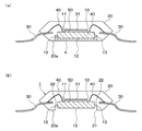
図1は、本発明の第1実施形態に係るモールドパッケージ1を放熱部材2に搭載したモールドパッケージ1の実装構造を示す概略断面図である。また、図2は、図1中のモールドパッケージ1の単体構成を示す図であり、(a)は概略平面図、(b)は概略断面図である。なお、図2(a)では、モールド樹脂20の外形を一点鎖線で示し、モールド樹脂20を透過してモールド樹脂20の内部に位置する構成要素を示している。
図5は、本発明の第2実施形態に係るモールドパッケージ1の実装構造の概略断面構成を示す図である。上記第1実施形態では、モールドパッケージ1を放熱部材2の一面2aに対してフェイスアップで搭載したが、本実施形態では、モールドパッケージ1を配線基板4にフェイスダウンで搭載しつつ放熱部材2の一面2aに対してフェイスアップで搭載したところが、上記第1実施形態とは相違するものである。
図7は、本発明の第3実施形態に係るモールドパッケージ1aの単体構成を示す図であり、(a)は概略平面図、(b)は概略断面図である。なお、図7(a)では、モールド樹脂20の外形を一点鎖線で示し、モールド樹脂20を透過してモールド樹脂20の内部に位置する構成要素を示している。
図9は、本発明の第4実施形態に係るモールドパッケージ1bを放熱部材2に搭載したモールドパッケージの実装構造を示す概略断面図である。
図12は、本発明の他の実施形態に係るモールドパッケージの概略断面図である。この図12に示されるものは、上記第4実施形態に示したノンリード構成において、モールド樹脂20の底面20aに位置するリード端子30を、さらにモールド樹脂20の側部からはみ出すように突出させたものである。
2 放熱部材
2a 放熱部材の一面
3 熱伝導性部材
10 半導体チップ
11 半導体チップの一面
12 半導体チップの他面
13 半導体チップの側面
20 モールド樹脂
20a モールド樹脂の底面
21 モールド樹脂の開口部
22 凹み部
31 アイランド
Claims (2)
- 板状の半導体チップ(10)の両板面のうち一面(11)側をモールド樹脂(20)で封止し、他面(12)を前記モールド樹脂(20)より露出させるようにしたモールドパッケージ(1)を、放熱部材(2)の一面(2a)に搭載し、
前記半導体チップ(10)の他面(12)と前記放熱部材(2)の一面(2a)との間に熱伝導性を有する熱伝導性部材(3)を介在させ、この熱伝導性部材(3)を介して前記半導体チップ(10)と前記放熱部材(2)とを熱的に接続してなるモールドパッケージの実装構造であって、
前記半導体チップ(10)の前記両板面(11、12)の外周端部に位置し前記半導体チップ(10)の板厚方向に延びる面である側面(13)が、前記モールド樹脂(20)より露出しており、
前記熱伝導性部材(3)は、前記半導体チップ(10)の前記他面(12)から前記側面(13)まで回り込むように配置されて、当該他面(12)および当該側面(13)に直接接触しており、
前記熱伝導性部材(3)を介して、前記半導体チップ(10)の前記他面(12)および前記側面(13)と前記放熱部材(2)とが熱的に接続されており、
前記モールド樹脂(20)は前記半導体チップ(10)の前記一面(11)から前記側面(13)の外側に回り込んで前記他面(12)側まで配置されており、
前記モールド樹脂(20)における前記半導体チップ(10)の前記他面(12)側に位置する外表面(20a)のうち前記半導体チップ(10)の前記他面(12)に対向する部位には、前記半導体チップ(10)の前記他面(12)を露出させる開口部(21)が設けられており、
前記開口部(21)の底部のうち前記半導体チップ(10)の前記他面(12)の外側に位置する部位は、前記半導体チップ(10)の前記他面(12)よりも凹んだ凹み部(22)となっており、
前記半導体チップ(10)の側面(13)は、前記凹み部(22)に臨んだ状態で前記モールド樹脂(20)より露出しており、
前記半導体チップ(10)の前記他面(12)は、前記モールド樹脂(20)における前記半導体チップ(10)の前記他面(12)側に位置する外表面(20a)よりも引っこんでおり、
前記熱伝導性部材(3)は、前記凹み部(22)を含む前記開口部(21)内に充填されており、
前記モールド樹脂(20)内にて、前記半導体チップ(10)の前記一面(11)には、前記半導体チップ(10)よりも小さい板状のアイランド(31)が接合され、前記半導体チップ(10)は前記アイランド(31)に支持されており、
前記モールド樹脂(20)内にて前記半導体チップ(10)の周囲には、リード端子(30)が設けられ、
さらに、前記モールド樹脂(20)内にて、前記半導体チップ(10)の前記一面(11)と前記リード端子(30)とが、ワイヤ(40)により接続されていることを特徴とするモールドパッケージの実装構造。 - 請求項1に記載の実装構造を形成するモールドパッケージ(1)の実装方法であって、
前記半導体チップ(10)の全体を前記モールド樹脂(20)で封止した後、前記モールド樹脂(20)のうち前記半導体チップ(10)の前記他面(12)および前記側面(13)を封止する部位を、レーザを照射して除去することにより、前記半導体チップ(10)の前記他面(12)および前記側面(13)を露出させ、
続いて、露出した前記半導体チップ(10)の前記他面(12)および前記側面(13)に前記レーザを照射して、これら各面を粗化する粗化処理を行い、
しかる後、粗化された前記半導体チップ(10)の前記他面(12)および前記側面(13)と前記放熱部材(2)との間に前記熱伝導性部材(3)を介在させつつ、前記モールドパッケージ(1)を前記放熱部材(2)の一面(2a)に搭載することを特徴とするモールドパッケージの実装方法。
Priority Applications (1)
| Application Number | Priority Date | Filing Date | Title |
|---|---|---|---|
| JP2009095538A JP5169964B2 (ja) | 2009-04-10 | 2009-04-10 | モールドパッケージの実装構造および実装方法 |
Applications Claiming Priority (1)
| Application Number | Priority Date | Filing Date | Title |
|---|---|---|---|
| JP2009095538A JP5169964B2 (ja) | 2009-04-10 | 2009-04-10 | モールドパッケージの実装構造および実装方法 |
Publications (2)
| Publication Number | Publication Date |
|---|---|
| JP2010245468A JP2010245468A (ja) | 2010-10-28 |
| JP5169964B2 true JP5169964B2 (ja) | 2013-03-27 |
Family
ID=43098115
Family Applications (1)
| Application Number | Title | Priority Date | Filing Date |
|---|---|---|---|
| JP2009095538A Expired - Fee Related JP5169964B2 (ja) | 2009-04-10 | 2009-04-10 | モールドパッケージの実装構造および実装方法 |
Country Status (1)
| Country | Link |
|---|---|
| JP (1) | JP5169964B2 (ja) |
Cited By (1)
| Publication number | Priority date | Publication date | Assignee | Title |
|---|---|---|---|---|
| CN103077901A (zh) * | 2013-02-06 | 2013-05-01 | 日月光半导体制造股份有限公司 | 半导体封装件的封装方法及应用其形成的半导体封装件 |
Families Citing this family (5)
| Publication number | Priority date | Publication date | Assignee | Title |
|---|---|---|---|---|
| JP5843539B2 (ja) * | 2011-09-16 | 2016-01-13 | 三菱電機株式会社 | 半導体装置及び当該半導体装置の製造方法 |
| JP6076675B2 (ja) * | 2011-10-31 | 2017-02-08 | ローム株式会社 | 半導体装置 |
| JP2016018979A (ja) | 2014-07-11 | 2016-02-01 | 株式会社デンソー | モールドパッケージ |
| JP6818801B2 (ja) * | 2019-04-01 | 2021-01-20 | ローム株式会社 | パワーモジュールおよびその製造方法 |
| EP4333046A1 (en) * | 2021-04-28 | 2024-03-06 | Sony Semiconductor Solutions Corporation | Semiconductor device |
Family Cites Families (8)
| Publication number | Priority date | Publication date | Assignee | Title |
|---|---|---|---|---|
| JPH02240953A (ja) * | 1989-03-14 | 1990-09-25 | Sharp Corp | 半導体装置 |
| JP3222660B2 (ja) * | 1993-10-26 | 2001-10-29 | 松下電工株式会社 | 基材表面の処理方法 |
| MY112145A (en) * | 1994-07-11 | 2001-04-30 | Ibm | Direct attachment of heat sink attached directly to flip chip using flexible epoxy |
| JPH1168016A (ja) * | 1997-08-12 | 1999-03-09 | Nec Corp | 樹脂封止型半導体装置 |
| JP2000236058A (ja) * | 1999-02-15 | 2000-08-29 | Matsushita Electronics Industry Corp | 半導体装置及びその製造方法 |
| JP2007180089A (ja) * | 2005-12-27 | 2007-07-12 | Auto Network Gijutsu Kenkyusho:Kk | 回路導体パターンを有する樹脂成形部品の製造方法 |
| JP4589269B2 (ja) * | 2006-06-16 | 2010-12-01 | ソニー株式会社 | 半導体装置およびその製造方法 |
| JP4963879B2 (ja) * | 2006-06-16 | 2012-06-27 | 株式会社ソニー・コンピュータエンタテインメント | 半導体装置および半導体装置の製造方法 |
-
2009
- 2009-04-10 JP JP2009095538A patent/JP5169964B2/ja not_active Expired - Fee Related
Cited By (2)
| Publication number | Priority date | Publication date | Assignee | Title |
|---|---|---|---|---|
| CN103077901A (zh) * | 2013-02-06 | 2013-05-01 | 日月光半导体制造股份有限公司 | 半导体封装件的封装方法及应用其形成的半导体封装件 |
| CN103077901B (zh) * | 2013-02-06 | 2015-10-28 | 日月光半导体制造股份有限公司 | 半导体封装件的封装方法及应用其形成的半导体封装件 |
Also Published As
| Publication number | Publication date |
|---|---|
| JP2010245468A (ja) | 2010-10-28 |
Similar Documents
| Publication | Publication Date | Title |
|---|---|---|
| EP2005470B1 (en) | Lead frame based, over-molded semiconductor package with integrated through hole technology (tht) heat spreader pin(s) and associated method of manufacturing | |
| JP5802695B2 (ja) | 半導体装置、半導体装置の製造方法 | |
| JP5149854B2 (ja) | 半導体装置 | |
| US8994161B2 (en) | Semiconductor device package and methods for producing same | |
| JP5169964B2 (ja) | モールドパッケージの実装構造および実装方法 | |
| JPH08306855A (ja) | 半導体パッケージ、リードフレーム、回路基板、半導体パッケージモールディング用金型及び電子回路盤並にリードフレームの製造方法 | |
| JP2005191147A (ja) | 混成集積回路装置の製造方法 | |
| JPH0473297B2 (ja) | ||
| JP2010109255A (ja) | 半導体装置 | |
| JPH0637217A (ja) | 半導体装置 | |
| JP2017028131A (ja) | パッケージ実装体 | |
| JP5119092B2 (ja) | 半導体装置の製造方法 | |
| JP2007150044A (ja) | 半導体装置 | |
| JPH06132441A (ja) | 樹脂封止型半導体装置及びその製造方法 | |
| JP2006278607A (ja) | 面実装タイプ樹脂製中空パッケージ及びこれを用いた半導体装置 | |
| JP4994883B2 (ja) | 樹脂封止型半導体装置 | |
| KR20020093250A (ko) | 리드 노출형 리드 프레임 및 그를 이용한 리드 노출형반도체 패키지 | |
| JP5385438B2 (ja) | 半導体装置 | |
| US20170018487A1 (en) | Thermal enhancement for quad flat no lead (qfn) packages | |
| JP2008288493A (ja) | 半導体装置 | |
| JP2009158825A (ja) | 半導体装置 | |
| KR100704311B1 (ko) | 내부리드 노출형 반도체 칩 패키지와 그 제조 방법 | |
| JP2002064174A (ja) | 半導体装置及びその製造方法 | |
| JPH07326690A (ja) | 半導体装置用パッケージおよび半導体装置 | |
| JP4326385B2 (ja) | 半導体装置 |
Legal Events
| Date | Code | Title | Description |
|---|---|---|---|
| A621 | Written request for application examination |
Free format text: JAPANESE INTERMEDIATE CODE: A621 Effective date: 20110624 |
|
| A977 | Report on retrieval |
Free format text: JAPANESE INTERMEDIATE CODE: A971007 Effective date: 20120727 |
|
| A131 | Notification of reasons for refusal |
Free format text: JAPANESE INTERMEDIATE CODE: A131 Effective date: 20120807 |
|
| A521 | Written amendment |
Free format text: JAPANESE INTERMEDIATE CODE: A523 Effective date: 20121004 |
|
| TRDD | Decision of grant or rejection written | ||
| A01 | Written decision to grant a patent or to grant a registration (utility model) |
Free format text: JAPANESE INTERMEDIATE CODE: A01 Effective date: 20121204 |
|
| A61 | First payment of annual fees (during grant procedure) |
Free format text: JAPANESE INTERMEDIATE CODE: A61 Effective date: 20121217 |
|
| R151 | Written notification of patent or utility model registration |
Ref document number: 5169964 Country of ref document: JP Free format text: JAPANESE INTERMEDIATE CODE: R151 |
|
| FPAY | Renewal fee payment (event date is renewal date of database) |
Free format text: PAYMENT UNTIL: 20160111 Year of fee payment: 3 |
|
| R250 | Receipt of annual fees |
Free format text: JAPANESE INTERMEDIATE CODE: R250 |
|
| R250 | Receipt of annual fees |
Free format text: JAPANESE INTERMEDIATE CODE: R250 |
|
| R250 | Receipt of annual fees |
Free format text: JAPANESE INTERMEDIATE CODE: R250 |
|
| LAPS | Cancellation because of no payment of annual fees |