JP5169964B2 - Mold package mounting structure and mounting method - Google Patents
Mold package mounting structure and mounting method Download PDFInfo
- Publication number
- JP5169964B2 JP5169964B2 JP2009095538A JP2009095538A JP5169964B2 JP 5169964 B2 JP5169964 B2 JP 5169964B2 JP 2009095538 A JP2009095538 A JP 2009095538A JP 2009095538 A JP2009095538 A JP 2009095538A JP 5169964 B2 JP5169964 B2 JP 5169964B2
- Authority
- JP
- Japan
- Prior art keywords
- semiconductor chip
- mold resin
- mold
- exposed
- package
- Prior art date
- Legal status (The legal status is an assumption and is not a legal conclusion. Google has not performed a legal analysis and makes no representation as to the accuracy of the status listed.)
- Expired - Fee Related
Links
Images


Classifications
-
- H—ELECTRICITY
- H01—ELECTRIC ELEMENTS
- H01L—SEMICONDUCTOR DEVICES NOT COVERED BY CLASS H10
- H01L24/00—Arrangements for connecting or disconnecting semiconductor or solid-state bodies; Methods or apparatus related thereto
- H01L24/93—Batch processes
- H01L24/95—Batch processes at chip-level, i.e. with connecting carried out on a plurality of singulated devices, i.e. on diced chips
- H01L24/97—Batch processes at chip-level, i.e. with connecting carried out on a plurality of singulated devices, i.e. on diced chips the devices being connected to a common substrate, e.g. interposer, said common substrate being separable into individual assemblies after connecting
-
- H—ELECTRICITY
- H01—ELECTRIC ELEMENTS
- H01L—SEMICONDUCTOR DEVICES NOT COVERED BY CLASS H10
- H01L2224/00—Indexing scheme for arrangements for connecting or disconnecting semiconductor or solid-state bodies and methods related thereto as covered by H01L24/00
- H01L2224/01—Means for bonding being attached to, or being formed on, the surface to be connected, e.g. chip-to-package, die-attach, "first-level" interconnects; Manufacturing methods related thereto
- H01L2224/26—Layer connectors, e.g. plate connectors, solder or adhesive layers; Manufacturing methods related thereto
- H01L2224/31—Structure, shape, material or disposition of the layer connectors after the connecting process
- H01L2224/32—Structure, shape, material or disposition of the layer connectors after the connecting process of an individual layer connector
- H01L2224/321—Disposition
- H01L2224/32151—Disposition the layer connector connecting between a semiconductor or solid-state body and an item not being a semiconductor or solid-state body, e.g. chip-to-substrate, chip-to-passive
- H01L2224/32221—Disposition the layer connector connecting between a semiconductor or solid-state body and an item not being a semiconductor or solid-state body, e.g. chip-to-substrate, chip-to-passive the body and the item being stacked
- H01L2224/32245—Disposition the layer connector connecting between a semiconductor or solid-state body and an item not being a semiconductor or solid-state body, e.g. chip-to-substrate, chip-to-passive the body and the item being stacked the item being metallic
-
- H—ELECTRICITY
- H01—ELECTRIC ELEMENTS
- H01L—SEMICONDUCTOR DEVICES NOT COVERED BY CLASS H10
- H01L2224/00—Indexing scheme for arrangements for connecting or disconnecting semiconductor or solid-state bodies and methods related thereto as covered by H01L24/00
- H01L2224/01—Means for bonding being attached to, or being formed on, the surface to be connected, e.g. chip-to-package, die-attach, "first-level" interconnects; Manufacturing methods related thereto
- H01L2224/42—Wire connectors; Manufacturing methods related thereto
- H01L2224/47—Structure, shape, material or disposition of the wire connectors after the connecting process
- H01L2224/48—Structure, shape, material or disposition of the wire connectors after the connecting process of an individual wire connector
- H01L2224/4805—Shape
- H01L2224/4809—Loop shape
- H01L2224/48091—Arched
-
- H—ELECTRICITY
- H01—ELECTRIC ELEMENTS
- H01L—SEMICONDUCTOR DEVICES NOT COVERED BY CLASS H10
- H01L2224/00—Indexing scheme for arrangements for connecting or disconnecting semiconductor or solid-state bodies and methods related thereto as covered by H01L24/00
- H01L2224/01—Means for bonding being attached to, or being formed on, the surface to be connected, e.g. chip-to-package, die-attach, "first-level" interconnects; Manufacturing methods related thereto
- H01L2224/42—Wire connectors; Manufacturing methods related thereto
- H01L2224/47—Structure, shape, material or disposition of the wire connectors after the connecting process
- H01L2224/48—Structure, shape, material or disposition of the wire connectors after the connecting process of an individual wire connector
- H01L2224/481—Disposition
- H01L2224/48151—Connecting between a semiconductor or solid-state body and an item not being a semiconductor or solid-state body, e.g. chip-to-substrate, chip-to-passive
- H01L2224/48221—Connecting between a semiconductor or solid-state body and an item not being a semiconductor or solid-state body, e.g. chip-to-substrate, chip-to-passive the body and the item being stacked
- H01L2224/48245—Connecting between a semiconductor or solid-state body and an item not being a semiconductor or solid-state body, e.g. chip-to-substrate, chip-to-passive the body and the item being stacked the item being metallic
- H01L2224/48247—Connecting between a semiconductor or solid-state body and an item not being a semiconductor or solid-state body, e.g. chip-to-substrate, chip-to-passive the body and the item being stacked the item being metallic connecting the wire to a bond pad of the item
-
- H—ELECTRICITY
- H01—ELECTRIC ELEMENTS
- H01L—SEMICONDUCTOR DEVICES NOT COVERED BY CLASS H10
- H01L2224/00—Indexing scheme for arrangements for connecting or disconnecting semiconductor or solid-state bodies and methods related thereto as covered by H01L24/00
- H01L2224/01—Means for bonding being attached to, or being formed on, the surface to be connected, e.g. chip-to-package, die-attach, "first-level" interconnects; Manufacturing methods related thereto
- H01L2224/42—Wire connectors; Manufacturing methods related thereto
- H01L2224/47—Structure, shape, material or disposition of the wire connectors after the connecting process
- H01L2224/48—Structure, shape, material or disposition of the wire connectors after the connecting process of an individual wire connector
- H01L2224/481—Disposition
- H01L2224/48151—Connecting between a semiconductor or solid-state body and an item not being a semiconductor or solid-state body, e.g. chip-to-substrate, chip-to-passive
- H01L2224/48221—Connecting between a semiconductor or solid-state body and an item not being a semiconductor or solid-state body, e.g. chip-to-substrate, chip-to-passive the body and the item being stacked
- H01L2224/48245—Connecting between a semiconductor or solid-state body and an item not being a semiconductor or solid-state body, e.g. chip-to-substrate, chip-to-passive the body and the item being stacked the item being metallic
- H01L2224/4826—Connecting between the body and an opposite side of the item with respect to the body
-
- H—ELECTRICITY
- H01—ELECTRIC ELEMENTS
- H01L—SEMICONDUCTOR DEVICES NOT COVERED BY CLASS H10
- H01L2224/00—Indexing scheme for arrangements for connecting or disconnecting semiconductor or solid-state bodies and methods related thereto as covered by H01L24/00
- H01L2224/01—Means for bonding being attached to, or being formed on, the surface to be connected, e.g. chip-to-package, die-attach, "first-level" interconnects; Manufacturing methods related thereto
- H01L2224/42—Wire connectors; Manufacturing methods related thereto
- H01L2224/47—Structure, shape, material or disposition of the wire connectors after the connecting process
- H01L2224/49—Structure, shape, material or disposition of the wire connectors after the connecting process of a plurality of wire connectors
- H01L2224/491—Disposition
- H01L2224/4912—Layout
- H01L2224/49171—Fan-out arrangements
-
- H—ELECTRICITY
- H01—ELECTRIC ELEMENTS
- H01L—SEMICONDUCTOR DEVICES NOT COVERED BY CLASS H10
- H01L2224/00—Indexing scheme for arrangements for connecting or disconnecting semiconductor or solid-state bodies and methods related thereto as covered by H01L24/00
- H01L2224/73—Means for bonding being of different types provided for in two or more of groups H01L2224/10, H01L2224/18, H01L2224/26, H01L2224/34, H01L2224/42, H01L2224/50, H01L2224/63, H01L2224/71
- H01L2224/732—Location after the connecting process
- H01L2224/73201—Location after the connecting process on the same surface
- H01L2224/73215—Layer and wire connectors
-
- H—ELECTRICITY
- H01—ELECTRIC ELEMENTS
- H01L—SEMICONDUCTOR DEVICES NOT COVERED BY CLASS H10
- H01L2224/00—Indexing scheme for arrangements for connecting or disconnecting semiconductor or solid-state bodies and methods related thereto as covered by H01L24/00
- H01L2224/73—Means for bonding being of different types provided for in two or more of groups H01L2224/10, H01L2224/18, H01L2224/26, H01L2224/34, H01L2224/42, H01L2224/50, H01L2224/63, H01L2224/71
- H01L2224/732—Location after the connecting process
- H01L2224/73251—Location after the connecting process on different surfaces
- H01L2224/73265—Layer and wire connectors
-
- H—ELECTRICITY
- H01—ELECTRIC ELEMENTS
- H01L—SEMICONDUCTOR DEVICES NOT COVERED BY CLASS H10
- H01L2224/00—Indexing scheme for arrangements for connecting or disconnecting semiconductor or solid-state bodies and methods related thereto as covered by H01L24/00
- H01L2224/93—Batch processes
- H01L2224/95—Batch processes at chip-level, i.e. with connecting carried out on a plurality of singulated devices, i.e. on diced chips
- H01L2224/97—Batch processes at chip-level, i.e. with connecting carried out on a plurality of singulated devices, i.e. on diced chips the devices being connected to a common substrate, e.g. interposer, said common substrate being separable into individual assemblies after connecting
-
- H—ELECTRICITY
- H01—ELECTRIC ELEMENTS
- H01L—SEMICONDUCTOR DEVICES NOT COVERED BY CLASS H10
- H01L2924/00—Indexing scheme for arrangements or methods for connecting or disconnecting semiconductor or solid-state bodies as covered by H01L24/00
- H01L2924/15—Details of package parts other than the semiconductor or other solid state devices to be connected
- H01L2924/151—Die mounting substrate
- H01L2924/156—Material
- H01L2924/15786—Material with a principal constituent of the material being a non metallic, non metalloid inorganic material
- H01L2924/15787—Ceramics, e.g. crystalline carbides, nitrides or oxides
-
- H—ELECTRICITY
- H01—ELECTRIC ELEMENTS
- H01L—SEMICONDUCTOR DEVICES NOT COVERED BY CLASS H10
- H01L2924/00—Indexing scheme for arrangements or methods for connecting or disconnecting semiconductor or solid-state bodies as covered by H01L24/00
- H01L2924/15—Details of package parts other than the semiconductor or other solid state devices to be connected
- H01L2924/181—Encapsulation
- H01L2924/1815—Shape
- H01L2924/1816—Exposing the passive side of the semiconductor or solid-state body
- H01L2924/18165—Exposing the passive side of the semiconductor or solid-state body of a wire bonded chip
Landscapes
- Engineering & Computer Science (AREA)
- Computer Hardware Design (AREA)
- Microelectronics & Electronic Packaging (AREA)
- Power Engineering (AREA)
- Lead Frames For Integrated Circuits (AREA)
- Cooling Or The Like Of Semiconductors Or Solid State Devices (AREA)
Description
本発明は、半導体チップをハーフモールドしてなるモールドパッケージを放熱部材に搭載してなる実装構造、および、そのようなモールドパッケージを放熱部材に実装する実装方法に関し、特に、半導体チップの他面をモールド樹脂より直接露出させたものに関する。 The present invention relates to a mounting structure in which a mold package obtained by half-molding a semiconductor chip is mounted on a heat radiating member, and a mounting method for mounting such a mold package on a heat radiating member. It relates to those exposed directly from the mold resin.
従来より、半導体チップをハーフモールドしてなるモールドパッケージ、いわゆるハーフモールド構造のものとしては、半導体チップをヒートシンクの一面側に接着し、そのヒートシンクの他面をモールド樹脂より露出させたものが主流である。そして、このパッケージは、シリコーンゲルなどの熱伝導性部材を介して、外部筐体等の放熱部材に熱的に接続されることにより、半導体チップの熱を放熱するようにしている。 Conventionally, as a mold package formed by half-molding a semiconductor chip, a so-called half-mold structure, a semiconductor chip is bonded to one surface of a heat sink and the other surface of the heat sink is exposed from a mold resin. is there. This package is configured to radiate the heat of the semiconductor chip by being thermally connected to a heat radiating member such as an external housing through a heat conductive member such as silicone gel.
一方で、放熱性に優れ且つ小型化されたハーフモールド構造のパッケージとして、板状の半導体チップの両板面のうちの一面側をモールド樹脂で封止し、当該一面とは反対側の他面を直接、モールド樹脂より露出させるようにしたものが提案されている(たとえば、特許文献1参照)。 On the other hand, as a half mold structure package having excellent heat dissipation and miniaturization, one side of both plate surfaces of the plate-like semiconductor chip is sealed with mold resin, and the other side opposite to the one side Has been proposed that is exposed directly from the mold resin (for example, see Patent Document 1).
本発明者は、上記特許文献1に記載されている半導体チップの他面をモールド樹脂より直接露出させたハーフモールド構造のパッケージを、放熱部材に熱的に接続する実装構造について、検討を行った。
The inventor has examined a mounting structure in which a half-molded package in which the other surface of the semiconductor chip described in
この実装構造は、モールド樹脂より露出する半導体チップの他面を放熱部材の一面に対向させつつ、半導体チップの他面と放熱部材の一面との間に熱伝導性部材を介在させた状態で、当該モールドパッケージを放熱部材の一面に搭載することにより形成される。それにより、熱伝導性部材を介して半導体チップと放熱部材とが熱的に接続される。 In this mounting structure, with the other surface of the semiconductor chip exposed from the mold resin facing one surface of the heat radiating member, a thermally conductive member is interposed between the other surface of the semiconductor chip and one surface of the heat radiating member. It is formed by mounting the mold package on one surface of the heat dissipation member. Thereby, the semiconductor chip and the heat radiating member are thermally connected via the heat conductive member.
しかしながら、この実装構造においては、半導体チップと熱伝導性部材とが直接接触して熱的に接続される放熱経路としては、半導体チップの他面の経路のみであり、充分な放熱性を得ることは難しい。 However, in this mounting structure, the heat dissipation path where the semiconductor chip and the thermally conductive member are in direct contact and thermally connected is only the path on the other surface of the semiconductor chip, and sufficient heat dissipation is obtained. Is difficult.
本発明は、上記問題に鑑みてなされたものであり、半導体チップの他面がモールド樹脂より直接露出しているハーフモールド構造のモールドパッケージを、熱伝導性部材を介して放熱部材に搭載する実装構造において、半導体チップと熱伝導性部材とが直接接触して熱的に接続される放熱経路を増加して、放熱性の向上を図ることを目的とする。 The present invention has been made in view of the above problems, and is a mounting in which a mold package having a half mold structure in which the other surface of a semiconductor chip is directly exposed from a mold resin is mounted on a heat dissipation member via a heat conductive member. In the structure, an object is to improve heat dissipation by increasing the heat dissipation path in which the semiconductor chip and the heat conductive member are in direct contact and thermally connected.
上記目的を達成するため、請求項1に記載の発明においては、まず、半導体チップ(10)の両板面(11、12)の外周端部に位置し半導体チップ(10)の板厚方向に延びる面である側面(13)が、モールド樹脂(20)より露出しており、熱伝導性部材(3)は、半導体チップ(10)の他面(12)から側面(13)まで回り込むように配置されて、当該他面(12)および当該側面(13)に直接接触しており、熱伝導性部材(3)を介して、半導体チップ(10)の他面(12)および側面(13)と放熱部材(2)とが、熱的に接続されていることを特徴としている。 In order to achieve the above object, in the first aspect of the present invention, first, the semiconductor chip (10) is positioned at the outer peripheral ends of the two plate surfaces (11, 12) in the thickness direction of the semiconductor chip (10). The side surface (13), which is the extending surface, is exposed from the mold resin (20), and the heat conductive member (3) goes around from the other surface (12) to the side surface (13) of the semiconductor chip (10). It is disposed and is in direct contact with the other surface (12) and the side surface (13), and the other surface (12) and the side surface (13) of the semiconductor chip (10) through the heat conductive member (3). The heat radiating member (2) is thermally connected.
それによれば、半導体チップ(10)の他面(12)に加えて側面(13)も、熱伝導性部材(3)に直接接触するから、半導体チップ(10)と熱伝導性部材(3)とが直接接触して熱的に接続される放熱経路を従来よりも増加して、放熱性の向上を図ることができる。 According to this, since the side surface (13) in addition to the other surface (12) of the semiconductor chip (10) is also in direct contact with the heat conductive member (3), the semiconductor chip (10) and the heat conductive member (3) The number of heat dissipation paths that are in direct contact with each other and thermally connected can be increased as compared with the prior art, thereby improving heat dissipation.
また、請求項1に記載の実装構造は、次のような点も特徴としている。 Also, the mounting structure according to 請 Motomeko 1 is characterized also a point as follows.
・モールド樹脂(20)は半導体チップ(10)の一面(11)から側面(13)の外側に回り込んで他面(12)側まで配置されており、モールド樹脂(20)における半導体チップ(10)の他面(12)側に位置する外表面(20a)のうち半導体チップ(10)の他面(12)に対向する部位には、半導体チップ(10)の他面(12)を露出させる開口部(21)が設けられていること。 The mold resin (20) is arranged from one surface (11) of the semiconductor chip (10) to the outside of the side surface (13) to the other surface (12) side, and the semiconductor chip (10 in the mold resin (20)) ) The other surface (12) of the semiconductor chip (10) is exposed at a portion of the outer surface (20a) located on the other surface (12) side that faces the other surface (12) of the semiconductor chip (10). An opening (21) is provided.
・開口部(21)の底部のうち半導体チップ(10)の他面(12)の外側に位置する部位は、半導体チップ(10)の他面(12)よりも凹んだ凹み部(22)となっており、半導体チップ(10)の側面(13)は、凹み部(22)に臨んだ状態でモールド樹脂(20)より露出していること。 -The part located in the outer side of the other surface (12) of the semiconductor chip (10) in the bottom of the opening (21) is a recessed portion (22) recessed from the other surface (12) of the semiconductor chip (10). The side surface (13) of the semiconductor chip (10) is exposed from the mold resin (20) in a state of facing the recess (22).
・半導体チップ(10)の他面(12)は、モールド樹脂(20)における半導体チップ(10)の他面(12)側に位置する外表面(20a)よりも引っこんでおり、熱伝導性部材(3)は、凹み部(22)を含む開口部(21)内に充填されていること。 The other surface (12) of the semiconductor chip (10) is recessed more than the outer surface (20a) located on the other surface (12) side of the semiconductor chip (10) in the mold resin (20), and is thermally conductive. The member (3) is filled in the opening (21) including the recess (22).
これらの点を特徴とする本発明の実装構造によれば、熱伝導性部材(3)は、引っこんでいる半導体チップ(10)の他面(12)および凹み部(22)を底部とする開口部(21)内に充填された状態となるから、この開口部(21)の外側にはみ出しにくくなる。 According to the mounting structure of the present invention characterized by these points, the thermally conductive member (3) has the other surface (12) and the recessed portion (22) of the recessed semiconductor chip (10) as the bottom. Since it will be in the state filled in the opening part (21), it will become difficult to protrude outside this opening part (21).
さらに、請求項1に記載の発明では、モールド樹脂(20)内にて、半導体チップ(10)の一面(11)には、半導体チップ(10)よりも小さい板状のアイランド(31)が接合され、半導体チップ(10)はアイランド(31)に支持されており、モールド樹脂(20)内にて半導体チップ(10)の周囲には、リード端子(30)が設けられ、さらに、モールド樹脂(20)内にて、半導体チップ(10)の一面(11)とリード端子(30)とが、ワイヤ(40)により接続されていることを特徴としている。
Furthermore , in the invention described in
それによれば、半導体チップ(10)をモールド樹脂(20)で封止する前に、半導体チップ(10)をアイランド(31)によって支持することが可能になるから、製造工程においてモールド封止前の半導体チップ(10)の取り扱いが容易になる。 According to this, before the semiconductor chip (10) is sealed with the mold resin (20), the semiconductor chip (10) can be supported by the island (31). The semiconductor chip (10) can be easily handled.
また、請求項2に記載の発明は、請求項1に記載の実装構造を形成するモールドパッケージ(1)の実装方法であって、以下の各工程を有するものである。
The invention described in
・半導体チップ(10)の全体をモールド樹脂(20)で封止した後、モールド樹脂(20)のうち半導体チップ(10)の他面(12)および側面(13)を封止する部位を、レーザを照射して除去することにより、半導体チップ(10)の他面(12)および側面(13)を露出させる工程。 -After sealing the whole semiconductor chip (10) with mold resin (20), the part which seals the other surface (12) and side surface (13) of the semiconductor chip (10) among mold resin (20), A step of exposing the other surface (12) and the side surface (13) of the semiconductor chip (10) by irradiating and removing the laser.
・続いて、露出した半導体チップ(10)の他面(12)および側面(13)にレーザを照射して、これら各面(12、13)を粗化する粗化処理を行う工程。 Subsequently, a step of performing a roughening process of irradiating the other surface (12) and the side surface (13) of the exposed semiconductor chip (10) with a laser to roughen each of the surfaces (12, 13).
・しかる後、粗化された半導体チップ(10)の他面(12)および側面(13)と放熱部材(2)との間に熱伝導性部材(3)を介在させつつ、モールドパッケージ(1)を放熱部材(2)の一面(2a)に搭載する工程。 Thereafter, while the heat conductive member (3) is interposed between the other surface (12) and the side surface (13) of the roughened semiconductor chip (10) and the heat radiating member (2), the mold package (1 ) Is mounted on one surface (2a) of the heat dissipating member (2).
これらの工程を有する本製造方法によれば、請求項1に記載の実装構造を適切に製造できるとともに、モールドパッケージ(1)においてモールド樹脂(20)より露出する半導体チップ(10)の他面(12)および側面(13)の比表面積を増加させることができ、放熱性の向上の点で好ましい。
According to this manufacturing method having these steps, the mounting structure according to
なお、特許請求の範囲およびこの欄で記載した各手段の括弧内の符号は、後述する実施形態に記載の具体的手段との対応関係を示す一例である。 In addition, the code | symbol in the bracket | parenthesis of each means described in the claim and this column is an example which shows a corresponding relationship with the specific means as described in embodiment mentioned later.
以下、本発明の実施形態について図に基づいて説明する。なお、以下の各実施形態相互において、互いに同一もしくは均等である部分には、説明の簡略化を図るべく、図中、同一符号を付してある。 Hereinafter, embodiments of the present invention will be described with reference to the drawings. In the following embodiments, parts that are the same or equivalent to each other are given the same reference numerals in the drawings in order to simplify the description.
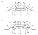
(第1実施形態)
図1は、本発明の第1実施形態に係るモールドパッケージ1を放熱部材2に搭載したモールドパッケージ1の実装構造を示す概略断面図である。また、図2は、図1中のモールドパッケージ1の単体構成を示す図であり、(a)は概略平面図、(b)は概略断面図である。なお、図2(a)では、モールド樹脂20の外形を一点鎖線で示し、モールド樹脂20を透過してモールド樹脂20の内部に位置する構成要素を示している。
(First embodiment)
FIG. 1 is a schematic cross-sectional view showing a mounting structure of a
本実施形態のモールドパッケージ1は、大きくは、板状の半導体チップ10の両板面11、12のうちの一面11側をモールド樹脂20で封止し、他面12をモールド樹脂20より露出させたハーフモールド構造を有するものである。
The
このモールドパッケージ1は、モールド樹脂20より露出する半導体チップ10の他面12を放熱部材2の一面2aに対向させつつ、放熱部材2の一面2aに搭載されている。そして、半導体チップ10の他面12と放熱部材2の一面2aとの間に、熱伝導性を有する熱伝導性部材3を介在させ、この熱伝導性部材3を介して半導体チップ10と放熱部材20とが熱的に接続されている。
The
半導体チップ10は、シリコン半導体などの半導体チップに、たとえば一般的な半導体プロセスによりトランジスタなどの素子を形成したICチップなどが挙げられる。この半導体チップ10は板状をなすが、ここでは一般的な半導体チップと同様、矩形板状をなしている。ここで、半導体チップ10の両板面11、12とは、半導体チップ10における表裏の面11、12つまり、板厚方向に直交する2個の主面11、12である。
Examples of the
また、半導体チップ10の周囲には、リード端子30が設けられている。ここでは、リード端子30は、一端部側を半導体チップ10に対向させつつ、他端部側が半導体チップ10とは反対側に延びるように配置されたものとされている。ここでは、リード端子30は複数本設けられており、これら複数本のものが半導体チップ10を中心として放射状をなすように設けられている。
A
このリード端子30は、Cuや42アロイなどの一般的なリードフレーム材料よりなり、導電性を有するものである。そして、モールド樹脂20の内部にて、リード端子30の一端部側すなわちインナーリードと半導体チップ10の一面11とは、ワイヤ40によって結線されており、このワイヤ40を介して、リード端子30と半導体チップ10とは電気的に接続されている。
The
このワイヤ40は、金やアルミニウムなどの一般的なワイヤボンディングにより形成されるものである。そして、リード端子30の他端部側は、アウターリードとしてモールド樹脂20から突出して露出している。
The
放熱部材2は、半導体チップ10からの熱を放熱する機能を有するとともに、半導体チップ10と電気的に接続されるものである。放熱部材2としては、アルミニウムや銅などの放熱性に優れた部材よりなる筺体が挙げられるが、上記放熱機能を有するならば、モールドパッケージ1を搭載する回路基板やバスバーなどであってもよい。
The
ここでは、図1に示されるように、モールドパッケージ1におけるリード端子30の上記アウターリードが放熱部材2の一面に電気的および機械的に接続されている。この接続は、図示しないが、はんだや導電性接着剤などにより行われている。それにより、半導体チップ10と放熱部材2とは、電気的信号のやりとりが可能となっている。
Here, as shown in FIG. 1, the outer leads of the
また、図1、図2に示されるように、モールド樹脂20内部にて、板状のアイランド31が半導体チップ10の一面11に接合され、半導体チップ10を支持している。このアイランド31は、後述する吊りリード32および上記リード端子30とともに、一般的なリードフレームよりなり、モールド樹脂20による封止後に、リードカットされてリード端子30と分離されるものである。
As shown in FIGS. 1 and 2, a plate-
アイランド31は、半導体チップ10の一面11よりもサイズの小さい矩形板状をなし、当該一面11の外形内に収まるように配置されている。このアイランド31と半導体チップ10の一面11とは、これら両者の間に介在するはんだや導電性接着剤などのダイボンド材50により接合され固定されている。
The
そして、図2(a)に示されるように、この矩形のアイランド31の四隅部には、当該四隅部から外方に突出して延びる吊りリード32が設けられている。吊りリード32の先端部は、半導体チップ10の一面11からはみ出してモールド樹脂20の外表面まで延びており、モールド樹脂20から露出している。
As shown in FIG. 2 (a), suspension leads 32 are provided at the four corners of the
この吊りリード32は、一般的なリードフレームにおけるものと同様に、モールド樹脂20による封止を行う前まで、アイランド31をリード端子30とともに図示しないリードフレームのフレーム部に一体化しておくものであり、当該封止後にカットされ当該フレーム部と分離されるものである。
As in the case of a general lead frame, the
ここで、本実施形態のモールドパッケージ1においては、半導体チップ10の他面12だけでなく半導体チップ10の側面13も、モールド樹脂20より露出する面とされている。
Here, in the
ここで、半導体チップ10の側面13とは、半導体チップ10の両板面11、12の外周端部に位置し半導体チップ10の板厚方向に延びる面13であり、ここでは、矩形板状をなす半導体チップ10の外周端部に位置する4個の面13である。さらに言うならば、半導体チップ10の側面13は、両板面11、12とは角部を介して隣接し当該両板面11、12とは交差して板厚方向に沿って延びる面13である。
Here, the
そして、熱伝導性部材3は、半導体チップ10の他面12から側面13まで回り込むように配置され、これら半導体チップ10の他面12および側面13に直接接触している。それにより、熱伝導性部材3を介して、半導体チップ10の他面12および側面13と放熱部材2とが熱的に接続されている。
The heat
この熱伝導性部材3は、モールド樹脂20よりも熱伝導性の高い樹脂よりなるゲルや接着剤、グリスなどである。モールド樹脂20は、一般的なエポキシ樹脂などのモールド材料よりなるが、熱伝導性部材3としては、たとえば、シリコーンゲルや、樹脂に銀や銅などの熱伝導性フィラーを含有させた接着剤(いわゆる熱伝導性接着剤)などが挙げられる。これらは、塗布することにより配設が行われるが、予めシート成形されたものを用いてもよい。
The heat
また、図1、図2に示されるように、本実施形態では、モールド樹脂20は、半導体チップ10の一面11を封止するだけでなく、半導体チップ10の一面11から側面13の外側に回り込んで他面12側まで配置されている。
As shown in FIGS. 1 and 2, in this embodiment, the
そして、モールド樹脂20においては、半導体チップ10の他面12側に位置する外表面20aのうち半導体チップ10の他面12に対向する部位が除去されて、半導体チップ10の他面12をモールド樹脂20より露出させる開口部21が設けられている。
In the
ここで、モールド樹脂20における半導体チップ10の他面12側に位置する外表面20aとは、本実施形態の実装構造においては、モールド樹脂20における放熱部材2の一面2aに対向する外表面20aである。以下、このモールド樹脂20における半導体チップ10の他面12側に位置する外表面20aを、モールド樹脂20の底面20aということにする。
Here, the
つまり、モールド樹脂20の底面20aのうち半導体チップ10の他面12に対向する部位に、半導体チップ10の他面12まで到達する開口した穴としての開口部21が形成されており、この開口部21を介して半導体チップ10の他面12がモールド樹脂20より露出している。
That is, an
また、この開口部21の底部のうち半導体チップ10の他面12の外側に位置する部位は、半導体チップ10の他面12よりも凹んだ凹み部22となっている。そして、半導体チップ10の側面13は、凹み部22に臨んだ状態でモールド樹脂20より露出している。言い換えれば、凹み部22によって半導体チップ10の側面13がモールド樹脂20と離れており、それにより、当該側面13がモールド樹脂20より露出している。
A portion of the bottom of the
さらに、図1、図2に示される例では、半導体チップ10の他面12は、モールド樹脂20の底面20aよりもモールド樹脂20の内部側に引っこんでいる。そして、熱伝導性部材3は、凹み部22を含む開口部21を埋めるように、当該開口部21内に充填されている。
Further, in the example shown in FIGS. 1 and 2, the
ここで、図1に示される実装構造においては、半導体チップ10の一面11がトランジスタなどの素子やワイヤ40との接続電極が形成された表面であり、他面12が裏面とされている。つまり、図1に示される実装構造は、半導体チップ10の表面11を放熱部材2の一面2aとは反対側に向けた搭載形態、いわゆるフェイスアップ実装の形態を採用している。
Here, in the mounting structure shown in FIG. 1, one
次に、本実施形態のモールドパッケージ1の実装構造を形成するモールドパッケージ1の実装方法の一具体例について、図3を参照して述べる。図3は、本実装方法のうちモールドパッケージ1におけるモールド樹脂20を除去する工程、すなわちモールド樹脂除去工程を示す工程図である。
Next, a specific example of the mounting method of the
まず、上記リード端子30、アイランド31および吊りリード32がパターニングされたリードフレームを用意する。そして、ダイボンド材50を介してアイランド31に半導体チップ10をその一面11側にて接合し、半導体チップ10をアイランド31に支持する。
First, a lead frame in which the
次に、半導体チップ10の一面11とその周囲に位置するリード端子30との間で、ワイヤボンディングを行い、半導体チップ10とリード端子30とをワイヤ40で結線し、接続する。
Next, wire bonding is performed between the one
その後、このものをモールド樹脂成形用の金型(図示せず)に設置し、リード端子30の上記アウターリードを除いて、半導体チップ10の全体、アイランド31、吊りリード32、リード端子30のインナーリードおよびワイヤ40を、モールド樹脂20で包み込むように封止する。
Thereafter, this is placed in a mold (not shown) for molding resin molding, and the outer lead of the
ここまでのワークの概略断面構成が図3(a)に示される。このワークにおいては、図3(a)に示されるように、半導体チップ10については、一面11、他面12および側面13、つまり半導体チップ10の外表面の全体がモールド樹脂20で被覆され、封止されている。
FIG. 3A shows a schematic cross-sectional configuration of the workpiece so far. In this work, as shown in FIG. 3A, for the
このように、半導体チップ10の全体をモールド樹脂20で封止した後、モールド樹脂20のうち半導体チップ10の他面12および側面13を封止する部位Kを除去する。この除去される部位Kは、図3(a)中のモールド樹脂20において、斜線ハッチングで示される部位Kである。
As described above, after the
具体的には、この部位Kに対して、レーザを照射して焼失させる。このようなレーザによるモールド樹脂20の除去は一般的なものであり、当該レーザとしては、YAGなどの半導体レーザが用いられる。こうして、図3(b)に示されるように、レーザを照射して当該部位Kを除去することにより、半導体チップ10の他面12および側面13をモールド樹脂20より露出させる。
Specifically, this portion K is burned off by irradiating with a laser. Such removal of the
本実施形態の実装方法では、さらに、露出した半導体チップ10の他面12および側面13に上記のレーザを照射して、これら各面12、13を粗化する粗化処理を行う。当該半導体10の各面12、13は当該レーザにより物理的に荒らされ、微細な凹凸が形成される。こうして、モールドパッケージ1ができあがる。
In the mounting method of this embodiment, the
その後、本実装方法では、モールドパッケージ1において、粗化された半導体チップ10の他面12および側面13と放熱部材2の一面2aとの間に熱伝導性部材3を介在させつつ、モールドパッケージ1を放熱部材2の一面2aに搭載する。この場合、熱伝導性部材3は、半導体チップ10の他面12および側面13側に塗布してもよいし、放熱部材2の一面2a側に塗布してもよい。
Thereafter, in this mounting method, in the
そして、場合に応じて、熱伝導性部材3に対して乾燥や加熱などの処理を行う。こうして、半導体チップ10の他面12および側面13と放熱部材2の一面2aとの間に介在する熱伝導性部材3を介して、モールドパッケージ1と放熱部材2とが熱的に接続され、実装構造が完成する。
And according to the case, processing, such as drying and a heating, is performed with respect to the heat
なお、ここでは、半導体チップ10の全体をモールド樹脂20で封止した後、モールド樹脂20のうち半導体チップ10の他面12および側面13を封止する部位Kを、レーザを照射して除去することにより、当該他面12および側面13を露出させたが、金型によって、これら各面12、13が露出するようにモールド樹脂20を成形してもよい。
Here, after the
ところで、本実施形態によれば、半導体チップ10の他面12に加えて半導体チップ10の側面13もモールド樹脂20より露出した面とされ、実装構造においては、熱伝導性部材3に直接接触する面となる。
By the way, according to the present embodiment, in addition to the
そのため、半導体チップ10と熱伝導性部材3とが直接接触して熱的に接続される放熱経路としては、従来の半導体チップの他面の経路のみである場合よりも増加し、放熱性の向上が実現される。
Therefore, the heat dissipation path in which the
また、上記図1に示される例では、半導体チップ10の他面12および凹み部22は、放熱部材2の一面2aに対向するモールド樹脂20の底面20aよりもモールド樹脂20の内部側に引っ込んでいる。
Further, in the example shown in FIG. 1, the
そして、モールド樹脂20においては、この引っこんでいる半導体チップ10の他面12および凹み部22を底部とする開口部21が形成されている。そして、この開口部21内に熱伝導性部材3が充填された状態とされているため、熱伝導性部材3は、この開口部21の外側にはみ出しにくくなる。
In the
その結果、熱伝導性部材3が、所望の領域、すなわち半導体チップ10の他面12および側面13に対向する領域から、大きくはみ出すのを防止することができる。ここで、モールド樹脂20における開口部21の開口縁部を、放熱部材2の一面2aに接触させれば、熱伝導部材3の開口部21からのはみ出し防止に好ましい。
As a result, it is possible to prevent the heat
また、本実施形態では、上記図1、図2に示されるように、モールド樹脂20内にて、半導体チップ10は、その一面11に接合された板状のアイランド31に支持されているため、半導体チップ10をモールド樹脂20で封止する前に、半導体チップ10をアイランド31によって支持することが可能になる。
In the present embodiment, as shown in FIGS. 1 and 2, the
これにより、たとえば、半導体チップ10とリード端子30との間でワイヤボンディングを行うときや、半導体チップ10をモールド樹脂成形用の金型に設置するときに、半導体チップ10の支持が安定する。このように、本実施形態によれば、製造工程においてモールド封止前の半導体チップ10の取り扱いが容易になる。
Thereby, for example, when wire bonding is performed between the
また、上記図3に示される製造方法によれば、モールド樹脂20の封止後、レーザ照射によるモールド樹脂20の除去を行って、半導体チップ10の他面12および側面13を露出させ、さらに、露出した当該各面12、13にレーザを照射して、これら各面12、13を粗化している。そのため、これら各面12、13の比表面積を増加させることができ、放熱性の向上の点で好ましい。
Further, according to the manufacturing method shown in FIG. 3, after sealing the
なお、上記図1に示される例では、半導体チップ10の他面12は、モールド樹脂20の底面20aよりもモールド樹脂20の内部側に引っこんでいたが、半導体チップ10の他面12とモールド樹脂20の底面20aとの位置関係は、これに限定されない。
In the example shown in FIG. 1, the
図4は、本実施形態における半導体チップ10の他面12とモールド樹脂20の底面20aとの位置関係のバリエーションを示す概略断面図である。図4(a)に示される例では、半導体チップ10の他面12とモールド樹脂20の底面20aとが同一平面に位置している。
FIG. 4 is a schematic cross-sectional view showing variations in the positional relationship between the
図4(b)に示される例では、半導体チップ10の他面12は、モールド樹脂20の開口部21にてモールド樹脂20の底面20aよりも突出している。そして、半導体チップ10の側面13は、モールド樹脂20の開口部21内に位置して露出する部位と、当該開口部21の外部に位置して露出する部位とが存在する。
In the example shown in FIG. 4B, the
また、図4(c)に示される例でも、半導体チップ10の他面12は、モールド樹脂20の底面20aよりも突出している。ここでは、モールド樹脂20に開口部21を設けておらず、また、半導体チップ10の側面13は、モールド樹脂20の凹みによる露出ではなく、半導体チップ10の他面12側の部位をモールド樹脂20から突出させることによって露出している。
In the example shown in FIG. 4C, the
そして、この図4に示される各例においても、モールド樹脂20より露出する半導体チップ10の他面12および側面13と放熱部材2の一面2aとの間に、熱伝導性部材3を介在させ、これによって、半導体チップ10と放熱部材2との熱的な接続が実現されている。
And also in each example shown by this FIG. 4, between the
なお、この図4の各例においても、上記したようなレーザ照射や金型による成形によって、モールド樹脂20を除去することにより、半導体チップ10の他面12および側面13を露出させることができる。
In each example of FIG. 4 also, the
(第2実施形態)
図5は、本発明の第2実施形態に係るモールドパッケージ1の実装構造の概略断面構成を示す図である。上記第1実施形態では、モールドパッケージ1を放熱部材2の一面2aに対してフェイスアップで搭載したが、本実施形態では、モールドパッケージ1を配線基板4にフェイスダウンで搭載しつつ放熱部材2の一面2aに対してフェイスアップで搭載したところが、上記第1実施形態とは相違するものである。
(Second Embodiment)
FIG. 5 is a diagram showing a schematic cross-sectional configuration of the mounting structure of the
この場合、図5に示されるように、モールドパッケージ1におけるリード端子30のアウターリードの曲げ方向をフェイスアップ実装の場合とは反対にする。具体的には、モールド樹脂20の側部から突出する当該アウターリードを、モールド樹脂20の底面20a方向とは反対の面方向に向けて曲げている。
In this case, as shown in FIG. 5, the bending direction of the outer lead of the
こうすることで、リード端子30のアウターリードは、配線基板4に接続されている。このアウターリードと配線基板4とは、図示しないはんだや導電性接着剤などを介して接合され、電気的・機械的に接続されている。ここで、配線基板4は、たとえばセラミック基板、プリント基板、リードフレームなどである。
By doing so, the outer leads of the
そして、放熱部材2は、モールドパッケージ1を挟んで配線基板4とは反対側に設けられている。そして、モールドパッケージ1は、モールド樹脂20の底面20aを放熱部材2の一面2aに対向させ、放熱部材20に対しては、フェイスアップの状態で搭載され、上記第1実施形態と同様の熱伝導性部材3を介した熱的な接続がなされている。
The
ここで、図6(a)、(b)は、本第2実施形態のモールド樹脂除去工程を示す工程図である。本実施形態のモールドパッケージ1も、上記第1実施形態と同様に、レーザ照射によるモールド樹脂20における部位Kの除去を行い、半導体チップ10の他面12および側面13を露出させることにより、作られる。
Here, FIGS. 6A and 6B are process diagrams showing the mold resin removing process of the second embodiment. Similarly to the first embodiment, the
そして、このモールドパッケージ1を、リード端子30のアウターリードを介して配線基板4に接続し、一方で、熱伝導性部材3を介して接続部材2の一面2aに接続すれば、上記図5に示されるモールドパッケージ1の実装構造ができあがる。本実施形態では、配線基板4にもパッケージ1が搭載されるものの、上記第1実施形態と同様の効果が期待できる。
Then, if this
なお、図5に示される例では、モールドパッケージ1は、モールド樹脂20に開口部21を設け、半導体チップ10の他面12をモールド樹脂20の底面20aよりも引っ込ませたものとしているが、本実施形態のモールドパッケージ1においても、半導体チップ10の他面12とモールド樹脂20の底面20aとの位置関係については、上記第1実施形態と同様のバリエーション(上記図4参照)が可能である。
In the example shown in FIG. 5, the
(第3実施形態)
図7は、本発明の第3実施形態に係るモールドパッケージ1aの単体構成を示す図であり、(a)は概略平面図、(b)は概略断面図である。なお、図7(a)では、モールド樹脂20の外形を一点鎖線で示し、モールド樹脂20を透過してモールド樹脂20の内部に位置する構成要素を示している。
(Third embodiment)
FIGS. 7A and 7B are diagrams showing a unit configuration of a
図7に示されるように、本実施形態では、モールドパッケージ1aにおいて、半導体チップ10を支持するアイランド31を省略した構成としたことが、上記第1実施形態のモールドパッケージ1とは相違するものである。
As shown in FIG. 7, in the present embodiment, the configuration in which the
この場合、半導体チップ10とリード端子30とをワイヤボンディングする工程、および、モールド樹脂20による封止工程では、半導体チップ10の他面12側にて、半導体チップ10とリード端子30とをテープなどに貼り付けて一体に連結すれば、半導体チップ10の支持が安定し、半導体チップ10とリード端子30との位置ずれなどを防止することができる。
In this case, in the step of wire bonding the
そして、モールド樹脂20の封止後は上記テープを剥がす。このテープの剥離に伴い、半導体チップ10の他面12が露出するが、側面13については上記したレーザ照射により露出させればよい。
Then, after sealing the
なお、ワイヤボンディング後に上記テープを剥がし、封止工程では、成型用の金型内に設けられた突起などの支持手段によって、半導体チップ10を当該金型内に支持するようにしてもよい。この場合には、半導体チップ10の他面12および側面13の両方をモールド樹脂20より露出させる方法として、レーザ照射による露出を採用してもよいし、金型成形による露出を採用してもよい。
Note that, after the wire bonding, the tape may be peeled off, and in the sealing step, the
図8は、本第3実施形態の他の例としてのモールドパッケージを示す概略断面図である。本実施形態においても、半導体チップ10の他面12とモールド樹脂20の底面20aとの位置関係については、上記第1実施形態と同様のバリエーションが可能である。
FIG. 8 is a schematic cross-sectional view showing a mold package as another example of the third embodiment. Also in the present embodiment, the positional relationship between the
上記図7に示した例では、モールド樹脂20の開口部21にて露出する半導体チップ10の他面12が、モールド樹脂20の底面20aから引っ込んでいたが、図8には、(a)開口部21から半導体チップ10の他面12がモールド樹脂20の底面20aよりも突出している例、(b)開口部21を持たずに半導体チップ10の他面12がモールド樹脂20の底面20aより突出している例が示されている。
In the example shown in FIG. 7, the
また、この図8に示されるように、モールド樹脂20の底面20aから半導体チップ10の他面12を突出させる場合、上記したレーザ照射や金型成形による方法を採用してもよいが、半導体チップ10の他面12側を上記テープにめり込ませた状態でモールド封止を行い、その後、上記テープを剥がす方法も採用可能である。
As shown in FIG. 8, when the
なお、アイランド31を持たない本実施形態のモールドパッケージ1aにおいても、上記第2実施形態と同様に、配線基板4にフェイスダウンで搭載しつつ放熱部材2の一面2aに対してフェイスアップで搭載する形態を採用してもよいことはもちろんである。
Note that, in the
(第4実施形態)
図9は、本発明の第4実施形態に係るモールドパッケージ1bを放熱部材2に搭載したモールドパッケージの実装構造を示す概略断面図である。
(Fourth embodiment)
FIG. 9 is a schematic sectional view showing a mounting structure of a mold package in which the mold package 1b according to the fourth embodiment of the present invention is mounted on the
上記各実施形態のモールドパッケージにおいては、リード端子30はモールド樹脂20から突出したアウターリードを有する構成であったが、本実施形態のモールドパッケージ1bにおいては、リード端子30がモールド樹脂20から突出するアウターリードを持たないノンリード構成である点が相違するものである。
In the mold package of each of the above embodiments, the
この場合、リード端子30は、モールド樹脂20の底面20aにて露出するものであり、その露出する面は、当該底面20aと実質同一平面に位置している。そして、このリード端子30の露出面は、はんだや導電性接着剤などの導電性接続部材60を介して、放熱部材2の一面2aと電気的に接続されている。
In this case, the
次に、本実施形態のモールドパッケージ1bの製造方法について、図10を参照して述べる。図10は、本第4実施形態に係るモールドパッケージの製造方法における(a)モールド樹脂除去工程、(b)ダイシング工程を示す工程図であり、各ワークは断面的に示されている。 Next, a method for manufacturing the mold package 1b of the present embodiment will be described with reference to FIG. FIG. 10 is a process diagram showing (a) a mold resin removing process and (b) a dicing process in the mold package manufacturing method according to the fourth embodiment, and each workpiece is shown in cross section.
本実施形態のパッケージ1bは、図10に示されるように、一般的なノンリードパッケージを型成形、ダイシングするMAP成形法により作製される。これは、複数の半導体チップをリードフレームに搭載して、一つのキャビティ内にて一括してモールド樹脂で封止した後に 、ダイシングして個々のパッケージを得る、というものである。 As shown in FIG. 10, the package 1b of this embodiment is manufactured by a MAP molding method in which a general non-lead package is molded and diced. In this method, a plurality of semiconductor chips are mounted on a lead frame, sealed in a single cavity with a mold resin, and then diced to obtain individual packages.
図10(a)には、モールド樹脂20にて封止した後のワークの状態が示されており、モールド樹脂20内では、隣り合うパッケージ間で連結されたリード端子30と半導体チップ10とがワイヤ40で結線されている。また、リード端子30のうちワイヤ40が接続されている面とは反対側の面が、モールド樹脂20より露出している。
FIG. 10A shows the state of the workpiece after sealing with the
この状態から、図10(a)中の斜線ハッチングで示される部位Kをレーザで切断する。いわゆるレーザダイシングを行う。この部位Kは、隣り合うパッケージ間では、モールド樹脂20だけでなくリード端子30の連結部も含むものであり、これにより、図10(b)に示されるように、ワークが個片化され、個々のモールドパッケージ1bができあがる。
From this state, a portion K indicated by hatching in FIG. 10A is cut with a laser. So-called laser dicing is performed. This portion K includes not only the
また、このレーザダイシングにおいては、パッケージ間だけでなく、モールド樹脂20のうち半導体チップ10の他面12および側面13を封止する部位Kにも、当該レーザを照射して当該部位Kを除去する。それにより、半導体チップ10の他面12および側面13をモールド樹脂20より露出させる。
In this laser dicing, not only between the packages but also the part K of the
このように、図10に示される方法によれば、MAP成形技術において、レーザダイシングを行うことにより、ダイシングによる個片化と、半導体チップ10の他面12および側面13の露出とを一括して行うことが可能となっている。
As described above, according to the method shown in FIG. 10, in the MAP molding technique, the laser dicing is performed, so that individualization by dicing and exposure of the
そして、このような製造方法を経てできあがった本実施形態のモールドパッケージ1bを、熱伝導性部材3および導電性接続部材60を介して、放熱部材2の一面2aに搭載すれば、上記図9に示される実装構造が完成する。そして、本実施形態の実装構造によっても、上記各実施形態の実装構造と同様に、半導体チップ10と熱伝導性部材3とが直接接触して熱的に接続される放熱経路が、従来よりも増加し、放熱性の向上が実現される。
And if the mold package 1b of this embodiment completed through such a manufacturing method is mounted on the one
また、半導体チップ10の他面12がモールド樹脂20の底面20aよりも引っこんでいることによる熱伝導性部材3のはみ出し防止、半導体チップ10の他面12および側面13をレーザ照射で粗化することによる放熱性向上についても、上記同様の効果が期待できる。
Moreover, the
なお、上記図10では、ダイシングおよびモールド樹脂20の除去の両方を、レーザで行ったが、ダイシングについては一般的なダイシングブレードによる切断を行ってもよい。また、半導体チップ10の他面12および側面13の露出については、モールド樹脂20の金型成形により行うようにしてもよい。
In FIG. 10, both dicing and removal of the
また、図11は、本第4実施形態の他の例としてのモールドパッケージを示す概略断面図である。本実施形態においても、半導体チップ10の他面12とモールド樹脂20の底面20aとの位置関係については、上記第1実施形態と同様のバリエーションが可能である。
FIG. 11 is a schematic cross-sectional view showing a mold package as another example of the fourth embodiment. Also in the present embodiment, the positional relationship between the
上記図9に示した例では、モールド樹脂20の開口部21にて露出する半導体チップ10の他面12が、モールド樹脂20の底面20aから引っ込んでいたが、図11には、開口部21を持たずに半導体チップ10の他面12がモールド樹脂20の底面20aより突出している例が示されている。さらに、当該バリエーションとしては、この図11に示される例以外にも、上記図4と同様の各種の形態が可能である。
In the example shown in FIG. 9, the
また、上記図9〜図11に示される例では、上記アイランド31を持たない構成を示しているが、本実施形態のモールドパッケージにおいても、モールド樹脂20内にて、半導体チップ10の一面11にアイランド31を接合し、半導体チップ10をアイランド31に支持するようにしてもよい。
In the example shown in FIGS. 9 to 11, the configuration without the
(他の実施形態)
図12は、本発明の他の実施形態に係るモールドパッケージの概略断面図である。この図12に示されるものは、上記第4実施形態に示したノンリード構成において、モールド樹脂20の底面20aに位置するリード端子30を、さらにモールド樹脂20の側部からはみ出すように突出させたものである。
(Other embodiments)
FIG. 12 is a schematic cross-sectional view of a mold package according to another embodiment of the present invention. In the non-lead configuration shown in the fourth embodiment, the one shown in FIG. 12 is one in which the
図12において、(a)は、モールド樹脂20の開口部21にて露出する半導体チップ10の他面12が、モールド樹脂20の底面20aから引っ込んでいる例であり、(b)は、開口部21を持たずに半導体チップ10の他面12がモールド樹脂20の底面20aより突出している例である。
12A is an example in which the
もちろん、この場合も、半導体チップ10の他面12とモールド樹脂20の底面20aとの位置関係については、図12に示される例以外にも、上記第1実施形態と同様のバリエーションが可能である。
Of course, in this case as well, the positional relationship between the
また、上記各実施形態のモールドパッケージは、半導体チップ10の放熱経路は、半導体チップ10の一面11側では形成されていなかったが、半導体チップ10の一面11にヒートシンク70を熱的に接続する両面放熱型のパッケージとしてもよい。
In the mold package of each of the above embodiments, the heat dissipation path of the
図13は、本発明のさらなる他の実施形態に係るモールドパッケージとしての両面放熱型のパッケージの一例を示す概略断面図である。これは、半導体チップ10の一面11におけるワイヤ40の接続部をモールド樹脂20で封止するものの、当該一面11のうち封止部位以外の部位に、ヒートシンク70を熱的に接続したものである。
FIG. 13 is a schematic cross-sectional view showing an example of a double-sided heat dissipation type package as a mold package according to still another embodiment of the present invention. In this case, the connection portion of the
このヒートシンク70と半導体チップ10の一面11との熱的および機械的な接続は、これらの間に介在するダイボンド材50によりなされる。そして、ヒートシンク70は、モールド樹脂20の底面20aとは反対側の面にて露出し、このヒートシンク70の露出面に放熱部材などを熱的に接続することにより、半導体チップ10の一面11側からも放熱が可能となる。
Thermal and mechanical connection between the
1 モールドパッケージ
2 放熱部材
2a 放熱部材の一面
3 熱伝導性部材
10 半導体チップ
11 半導体チップの一面
12 半導体チップの他面
13 半導体チップの側面
20 モールド樹脂
20a モールド樹脂の底面
21 モールド樹脂の開口部
22 凹み部
31 アイランド
DESCRIPTION OF
Claims (2)
前記半導体チップ(10)の他面(12)と前記放熱部材(2)の一面(2a)との間に熱伝導性を有する熱伝導性部材(3)を介在させ、この熱伝導性部材(3)を介して前記半導体チップ(10)と前記放熱部材(2)とを熱的に接続してなるモールドパッケージの実装構造であって、
前記半導体チップ(10)の前記両板面(11、12)の外周端部に位置し前記半導体チップ(10)の板厚方向に延びる面である側面(13)が、前記モールド樹脂(20)より露出しており、
前記熱伝導性部材(3)は、前記半導体チップ(10)の前記他面(12)から前記側面(13)まで回り込むように配置されて、当該他面(12)および当該側面(13)に直接接触しており、
前記熱伝導性部材(3)を介して、前記半導体チップ(10)の前記他面(12)および前記側面(13)と前記放熱部材(2)とが熱的に接続されており、
前記モールド樹脂(20)は前記半導体チップ(10)の前記一面(11)から前記側面(13)の外側に回り込んで前記他面(12)側まで配置されており、
前記モールド樹脂(20)における前記半導体チップ(10)の前記他面(12)側に位置する外表面(20a)のうち前記半導体チップ(10)の前記他面(12)に対向する部位には、前記半導体チップ(10)の前記他面(12)を露出させる開口部(21)が設けられており、
前記開口部(21)の底部のうち前記半導体チップ(10)の前記他面(12)の外側に位置する部位は、前記半導体チップ(10)の前記他面(12)よりも凹んだ凹み部(22)となっており、
前記半導体チップ(10)の側面(13)は、前記凹み部(22)に臨んだ状態で前記モールド樹脂(20)より露出しており、
前記半導体チップ(10)の前記他面(12)は、前記モールド樹脂(20)における前記半導体チップ(10)の前記他面(12)側に位置する外表面(20a)よりも引っこんでおり、
前記熱伝導性部材(3)は、前記凹み部(22)を含む前記開口部(21)内に充填されており、
前記モールド樹脂(20)内にて、前記半導体チップ(10)の前記一面(11)には、前記半導体チップ(10)よりも小さい板状のアイランド(31)が接合され、前記半導体チップ(10)は前記アイランド(31)に支持されており、
前記モールド樹脂(20)内にて前記半導体チップ(10)の周囲には、リード端子(30)が設けられ、
さらに、前記モールド樹脂(20)内にて、前記半導体チップ(10)の前記一面(11)と前記リード端子(30)とが、ワイヤ(40)により接続されていることを特徴とするモールドパッケージの実装構造。 A mold package in which one surface (11) side of both plate surfaces of the plate-shaped semiconductor chip (10) is sealed with the mold resin (20) and the other surface (12) is exposed from the mold resin (20). (1) is mounted on one surface (2a) of the heat dissipation member (2),
A thermally conductive member (3) having thermal conductivity is interposed between the other surface (12) of the semiconductor chip (10) and one surface (2a) of the heat radiating member (2), and this thermally conductive member ( 3) a mold package mounting structure in which the semiconductor chip (10) and the heat dissipating member (2) are thermally connected via
A side surface (13) which is a surface located at the outer peripheral end of the both plate surfaces (11, 12) of the semiconductor chip (10) and extending in the plate thickness direction of the semiconductor chip (10) is the mold resin (20). More exposed,
The heat conductive member (3) is arranged so as to go around from the other surface (12) of the semiconductor chip (10) to the side surface (13), and on the other surface (12) and the side surface (13). In direct contact,
The other surface (12) and the side surface (13) of the semiconductor chip (10) and the heat dissipating member (2) are thermally connected through the heat conductive member (3) ,
The mold resin (20) is disposed from the one surface (11) of the semiconductor chip (10) to the outside of the side surface (13) to the other surface (12) side,
Of the outer surface (20a) located on the other surface (12) side of the semiconductor chip (10) in the mold resin (20), the portion facing the other surface (12) of the semiconductor chip (10) An opening (21) for exposing the other surface (12) of the semiconductor chip (10) is provided;
A portion of the bottom of the opening (21) located outside the other surface (12) of the semiconductor chip (10) is a recessed portion recessed from the other surface (12) of the semiconductor chip (10). (22)
The side surface (13) of the semiconductor chip (10) is exposed from the mold resin (20) in a state of facing the recess (22),
The other surface (12) of the semiconductor chip (10) is recessed from an outer surface (20a) located on the other surface (12) side of the semiconductor chip (10) in the mold resin (20). ,
The thermally conductive member (3) is filled in the opening (21) including the recess (22),
In the mold resin (20), a plate-like island (31) smaller than the semiconductor chip (10) is bonded to the one surface (11) of the semiconductor chip (10), and the semiconductor chip (10). ) Is supported by the island (31),
A lead terminal (30) is provided around the semiconductor chip (10) in the mold resin (20).
Further, in the mold resin (20), the one surface (11) of the semiconductor chip (10) and the lead terminal (30) are connected by a wire (40). Implementation structure.
前記半導体チップ(10)の全体を前記モールド樹脂(20)で封止した後、前記モールド樹脂(20)のうち前記半導体チップ(10)の前記他面(12)および前記側面(13)を封止する部位を、レーザを照射して除去することにより、前記半導体チップ(10)の前記他面(12)および前記側面(13)を露出させ、
続いて、露出した前記半導体チップ(10)の前記他面(12)および前記側面(13)に前記レーザを照射して、これら各面を粗化する粗化処理を行い、
しかる後、粗化された前記半導体チップ(10)の前記他面(12)および前記側面(13)と前記放熱部材(2)との間に前記熱伝導性部材(3)を介在させつつ、前記モールドパッケージ(1)を前記放熱部材(2)の一面(2a)に搭載することを特徴とするモールドパッケージの実装方法。 A method for mounting a mold package (1) for forming the mounting structure according to claim 1 ,
After sealing the whole of the semiconductor chip (10) with the mold resin (20), the other surface (12) and the side surface (13) of the semiconductor chip (10) of the mold resin (20) are sealed. The portion to be stopped is removed by irradiating a laser to expose the other surface (12) and the side surface (13) of the semiconductor chip (10),
Subsequently, the other surface (12) and the side surface (13) of the exposed semiconductor chip (10) are irradiated with the laser, and a roughening process for roughening each of these surfaces is performed.
Thereafter, while interposing the thermally conductive member (3) between the other surface (12) and the side surface (13) of the roughened semiconductor chip (10) and the heat radiating member (2), A mold package mounting method comprising mounting the mold package (1) on one surface (2a) of the heat dissipation member (2).
Priority Applications (1)
| Application Number | Priority Date | Filing Date | Title |
|---|---|---|---|
| JP2009095538A JP5169964B2 (en) | 2009-04-10 | 2009-04-10 | Mold package mounting structure and mounting method |
Applications Claiming Priority (1)
| Application Number | Priority Date | Filing Date | Title |
|---|---|---|---|
| JP2009095538A JP5169964B2 (en) | 2009-04-10 | 2009-04-10 | Mold package mounting structure and mounting method |
Publications (2)
| Publication Number | Publication Date |
|---|---|
| JP2010245468A JP2010245468A (en) | 2010-10-28 |
| JP5169964B2 true JP5169964B2 (en) | 2013-03-27 |
Family
ID=43098115
Family Applications (1)
| Application Number | Title | Priority Date | Filing Date |
|---|---|---|---|
| JP2009095538A Expired - Fee Related JP5169964B2 (en) | 2009-04-10 | 2009-04-10 | Mold package mounting structure and mounting method |
Country Status (1)
| Country | Link |
|---|---|
| JP (1) | JP5169964B2 (en) |
Cited By (1)
| Publication number | Priority date | Publication date | Assignee | Title |
|---|---|---|---|---|
| CN103077901A (en) * | 2013-02-06 | 2013-05-01 | 日月光半导体制造股份有限公司 | Packaging method of semiconductor packaging member and semiconductor packaging member formed by applying packaging method |
Families Citing this family (5)
| Publication number | Priority date | Publication date | Assignee | Title |
|---|---|---|---|---|
| JP5843539B2 (en) * | 2011-09-16 | 2016-01-13 | 三菱電機株式会社 | Semiconductor device and method for manufacturing the same |
| JP6076675B2 (en) * | 2011-10-31 | 2017-02-08 | ローム株式会社 | Semiconductor device |
| JP2016018979A (en) | 2014-07-11 | 2016-02-01 | 株式会社デンソー | Mold package |
| JP6818801B2 (en) * | 2019-04-01 | 2021-01-20 | ローム株式会社 | Power module and its manufacturing method |
| EP4333046A1 (en) * | 2021-04-28 | 2024-03-06 | Sony Semiconductor Solutions Corporation | Semiconductor device |
Family Cites Families (8)
| Publication number | Priority date | Publication date | Assignee | Title |
|---|---|---|---|---|
| JPH02240953A (en) * | 1989-03-14 | 1990-09-25 | Sharp Corp | Semiconductor device |
| JP3222660B2 (en) * | 1993-10-26 | 2001-10-29 | 松下電工株式会社 | Substrate surface treatment method |
| MY112145A (en) * | 1994-07-11 | 2001-04-30 | Ibm | Direct attachment of heat sink attached directly to flip chip using flexible epoxy |
| JPH1168016A (en) * | 1997-08-12 | 1999-03-09 | Nec Corp | Resin-sealed semiconductor device |
| JP2000236058A (en) * | 1999-02-15 | 2000-08-29 | Matsushita Electronics Industry Corp | Semiconductor device and its manufacture |
| JP2007180089A (en) * | 2005-12-27 | 2007-07-12 | Auto Network Gijutsu Kenkyusho:Kk | Manufacturing method of resin molded component with circuit conductor pattern |
| JP4589269B2 (en) * | 2006-06-16 | 2010-12-01 | ソニー株式会社 | Semiconductor device and manufacturing method thereof |
| JP4963879B2 (en) * | 2006-06-16 | 2012-06-27 | 株式会社ソニー・コンピュータエンタテインメント | Semiconductor device and manufacturing method of semiconductor device |
-
2009
- 2009-04-10 JP JP2009095538A patent/JP5169964B2/en not_active Expired - Fee Related
Cited By (2)
| Publication number | Priority date | Publication date | Assignee | Title |
|---|---|---|---|---|
| CN103077901A (en) * | 2013-02-06 | 2013-05-01 | 日月光半导体制造股份有限公司 | Packaging method of semiconductor packaging member and semiconductor packaging member formed by applying packaging method |
| CN103077901B (en) * | 2013-02-06 | 2015-10-28 | 日月光半导体制造股份有限公司 | The method for packing of semiconductor package part and apply its semiconductor package part formed |
Also Published As
| Publication number | Publication date |
|---|---|
| JP2010245468A (en) | 2010-10-28 |
Similar Documents
| Publication | Publication Date | Title |
|---|---|---|
| EP2005470B1 (en) | Lead frame based, over-molded semiconductor package with integrated through hole technology (tht) heat spreader pin(s) and associated method of manufacturing | |
| JP5802695B2 (en) | Semiconductor device and method for manufacturing semiconductor device | |
| JP5149854B2 (en) | Semiconductor device | |
| US8994161B2 (en) | Semiconductor device package and methods for producing same | |
| JP5169964B2 (en) | Mold package mounting structure and mounting method | |
| JPH08306855A (en) | Semiconductor package,lead frame,circuit board,metallic moldfor molding semiconductor package,electronic circuit board and manufacture of lead frame | |
| JP2005191147A (en) | Method for manufacturing hybrid integrated circuit device | |
| JPH0473297B2 (en) | ||
| JP2010109255A (en) | Semiconductor device | |
| JPH0637217A (en) | Semiconductor device | |
| JP2017028131A (en) | Package mounting body | |
| JP5119092B2 (en) | Manufacturing method of semiconductor device | |
| JP2007150044A (en) | Semiconductor device | |
| JPH06132441A (en) | Resin-sealed semiconductor device and manufacture thereof | |
| JP2006278607A (en) | Surface-mounting resin-made hollow package and semiconductor device using the same | |
| JP4994883B2 (en) | Resin-sealed semiconductor device | |
| KR20020093250A (en) | ELP type leadframe and ELP using the same | |
| JP5385438B2 (en) | Semiconductor device | |
| US20170018487A1 (en) | Thermal enhancement for quad flat no lead (qfn) packages | |
| JP2008288493A (en) | Semiconductor device | |
| JP2009158825A (en) | Semiconductor device | |
| KR100704311B1 (en) | Semiconductor chip package having exposed inner lead and manufacturing method thereof | |
| JP2002064174A (en) | Semiconductor device and its manufacturing method | |
| JPH07326690A (en) | Package for semiconductor device and semiconductor device | |
| JP4326385B2 (en) | Semiconductor device |
Legal Events
| Date | Code | Title | Description |
|---|---|---|---|
| A621 | Written request for application examination |
Free format text: JAPANESE INTERMEDIATE CODE: A621 Effective date: 20110624 |
|
| A977 | Report on retrieval |
Free format text: JAPANESE INTERMEDIATE CODE: A971007 Effective date: 20120727 |
|
| A131 | Notification of reasons for refusal |
Free format text: JAPANESE INTERMEDIATE CODE: A131 Effective date: 20120807 |
|
| A521 | Written amendment |
Free format text: JAPANESE INTERMEDIATE CODE: A523 Effective date: 20121004 |
|
| TRDD | Decision of grant or rejection written | ||
| A01 | Written decision to grant a patent or to grant a registration (utility model) |
Free format text: JAPANESE INTERMEDIATE CODE: A01 Effective date: 20121204 |
|
| A61 | First payment of annual fees (during grant procedure) |
Free format text: JAPANESE INTERMEDIATE CODE: A61 Effective date: 20121217 |
|
| R151 | Written notification of patent or utility model registration |
Ref document number: 5169964 Country of ref document: JP Free format text: JAPANESE INTERMEDIATE CODE: R151 |
|
| FPAY | Renewal fee payment (event date is renewal date of database) |
Free format text: PAYMENT UNTIL: 20160111 Year of fee payment: 3 |
|
| R250 | Receipt of annual fees |
Free format text: JAPANESE INTERMEDIATE CODE: R250 |
|
| R250 | Receipt of annual fees |
Free format text: JAPANESE INTERMEDIATE CODE: R250 |
|
| R250 | Receipt of annual fees |
Free format text: JAPANESE INTERMEDIATE CODE: R250 |
|
| LAPS | Cancellation because of no payment of annual fees |