JP2017028131A - Package mounting body - Google Patents
Package mounting body Download PDFInfo
- Publication number
- JP2017028131A JP2017028131A JP2015146070A JP2015146070A JP2017028131A JP 2017028131 A JP2017028131 A JP 2017028131A JP 2015146070 A JP2015146070 A JP 2015146070A JP 2015146070 A JP2015146070 A JP 2015146070A JP 2017028131 A JP2017028131 A JP 2017028131A
- Authority
- JP
- Japan
- Prior art keywords
- semiconductor element
- exposed
- island
- package
- mold resin
- Prior art date
- Legal status (The legal status is an assumption and is not a legal conclusion. Google has not performed a legal analysis and makes no representation as to the accuracy of the status listed.)
- Pending
Links
Images


Classifications
-
- H—ELECTRICITY
- H01—ELECTRIC ELEMENTS
- H01L—SEMICONDUCTOR DEVICES NOT COVERED BY CLASS H10
- H01L2224/00—Indexing scheme for arrangements for connecting or disconnecting semiconductor or solid-state bodies and methods related thereto as covered by H01L24/00
- H01L2224/01—Means for bonding being attached to, or being formed on, the surface to be connected, e.g. chip-to-package, die-attach, "first-level" interconnects; Manufacturing methods related thereto
- H01L2224/42—Wire connectors; Manufacturing methods related thereto
- H01L2224/47—Structure, shape, material or disposition of the wire connectors after the connecting process
- H01L2224/48—Structure, shape, material or disposition of the wire connectors after the connecting process of an individual wire connector
- H01L2224/4805—Shape
- H01L2224/4809—Loop shape
- H01L2224/48091—Arched
-
- H—ELECTRICITY
- H01—ELECTRIC ELEMENTS
- H01L—SEMICONDUCTOR DEVICES NOT COVERED BY CLASS H10
- H01L2224/00—Indexing scheme for arrangements for connecting or disconnecting semiconductor or solid-state bodies and methods related thereto as covered by H01L24/00
- H01L2224/01—Means for bonding being attached to, or being formed on, the surface to be connected, e.g. chip-to-package, die-attach, "first-level" interconnects; Manufacturing methods related thereto
- H01L2224/42—Wire connectors; Manufacturing methods related thereto
- H01L2224/47—Structure, shape, material or disposition of the wire connectors after the connecting process
- H01L2224/48—Structure, shape, material or disposition of the wire connectors after the connecting process of an individual wire connector
- H01L2224/481—Disposition
- H01L2224/48151—Connecting between a semiconductor or solid-state body and an item not being a semiconductor or solid-state body, e.g. chip-to-substrate, chip-to-passive
- H01L2224/48221—Connecting between a semiconductor or solid-state body and an item not being a semiconductor or solid-state body, e.g. chip-to-substrate, chip-to-passive the body and the item being stacked
- H01L2224/48245—Connecting between a semiconductor or solid-state body and an item not being a semiconductor or solid-state body, e.g. chip-to-substrate, chip-to-passive the body and the item being stacked the item being metallic
- H01L2224/48247—Connecting between a semiconductor or solid-state body and an item not being a semiconductor or solid-state body, e.g. chip-to-substrate, chip-to-passive the body and the item being stacked the item being metallic connecting the wire to a bond pad of the item
-
- H—ELECTRICITY
- H01—ELECTRIC ELEMENTS
- H01L—SEMICONDUCTOR DEVICES NOT COVERED BY CLASS H10
- H01L2224/00—Indexing scheme for arrangements for connecting or disconnecting semiconductor or solid-state bodies and methods related thereto as covered by H01L24/00
- H01L2224/73—Means for bonding being of different types provided for in two or more of groups H01L2224/10, H01L2224/18, H01L2224/26, H01L2224/34, H01L2224/42, H01L2224/50, H01L2224/63, H01L2224/71
- H01L2224/732—Location after the connecting process
- H01L2224/73251—Location after the connecting process on different surfaces
- H01L2224/73265—Layer and wire connectors
-
- H—ELECTRICITY
- H01—ELECTRIC ELEMENTS
- H01L—SEMICONDUCTOR DEVICES NOT COVERED BY CLASS H10
- H01L2224/00—Indexing scheme for arrangements for connecting or disconnecting semiconductor or solid-state bodies and methods related thereto as covered by H01L24/00
- H01L2224/91—Methods for connecting semiconductor or solid state bodies including different methods provided for in two or more of groups H01L2224/80 - H01L2224/90
- H01L2224/92—Specific sequence of method steps
- H01L2224/922—Connecting different surfaces of the semiconductor or solid-state body with connectors of different types
- H01L2224/9222—Sequential connecting processes
- H01L2224/92242—Sequential connecting processes the first connecting process involving a layer connector
- H01L2224/92247—Sequential connecting processes the first connecting process involving a layer connector the second connecting process involving a wire connector
Abstract
Description
本発明は、アイランドに半導体素子を搭載し、アイランドにおける半導体素子とは反対側の面が露出するように、モールド樹脂による封止を行ったハーフモールドタイプの半導体パッケージを、アイランドにおける露出面とは反対側に配置された配線基板上に搭載してなるパッケージ実装体に関する。 The present invention provides a half mold type semiconductor package in which a semiconductor element is mounted on an island and sealed with a mold resin so that a surface opposite to the semiconductor element in the island is exposed. The present invention relates to a package mounting body mounted on a wiring board disposed on the opposite side.
従来より、この種のパッケージ実装体としては、たとえば特許文献1に記載のものが提案されている。ここで、半導体パッケージは、半導体素子の表裏の主面の一面を配線基板に対向させ、他面側に金属製のアイランドを接続したものを、モールド樹脂で封止してなる。
Conventionally, as this type of package mounting body, for example, the one described in
さらに、この半導体パッケージでは、アイランドのうち半導体素子とは反対側の面をモールド樹脂より露出させる、いわゆるハーフモールドの封止形態を採用している。そして、このアイランドの露出面にて、半導体素子の熱を放熱するようになっている。 Further, in this semiconductor package, a so-called half-mold sealing form is adopted in which the surface of the island opposite to the semiconductor element is exposed from the mold resin. Then, the heat of the semiconductor element is radiated on the exposed surface of the island.
ここで、特許文献1では、半導体パッケージを挟んで配線基板とは反対側に冷却部材が配置されている。そして、この冷却部材に対し、グリス等の熱伝導部材を介して、アイランドの露出面が熱的に接続されている。なお、このような冷却部材は、たとえば金属製のケース等であり、半導体素子の熱は、アイランドを介して冷却部材へ放熱される。
Here, in
また、この種の半導体パッケージでは、モールド樹脂内において半導体素子の外側にリード端子が設けられている。そして、このリード端子と半導体素子の一面とは、ワイヤボンディング等により電気的に接続されている。また、リード端子のアウターリード部は、モールド樹脂より配線基板の一面に向かって突出し、はんだ等の導電性接合材を介して、配線基板の一面に機械的および電気的に接続されている。 In this type of semiconductor package, lead terminals are provided outside the semiconductor element in the mold resin. The lead terminal and one surface of the semiconductor element are electrically connected by wire bonding or the like. In addition, the outer lead portion of the lead terminal protrudes from the mold resin toward one surface of the wiring board, and is mechanically and electrically connected to one surface of the wiring board via a conductive bonding material such as solder.
こうして、半導体パッケージと配線基板との電気的接続がなされている。これにより、半導体パッケージの熱は、アイランドを介して冷却部材へ放熱されるとともに、半導体パッケージと配線基板との間では、リード端子を介して電気的なやりとりが可能とされている。 Thus, electrical connection between the semiconductor package and the wiring board is made. Thereby, the heat of the semiconductor package is radiated to the cooling member via the island, and electrical exchange is possible between the semiconductor package and the wiring board via the lead terminal.
ところで、この種の実装体においては、半導体パッケージと配線基板との線膨張係数差等に起因して、リード端子のアウターリード部と配線基板との接続部に応力が発生する。しかし、当該接続部に発生する応力は、実質的にアウターリード部における長さ方向の変形によって吸収され緩和される。 By the way, in this type of mounting body, stress is generated in the connection portion between the outer lead portion of the lead terminal and the wiring substrate due to a difference in linear expansion coefficient between the semiconductor package and the wiring substrate. However, the stress generated in the connection portion is substantially absorbed and relaxed by the deformation in the length direction of the outer lead portion.
一方、近年の半導体パッケージの小型化に伴い、リード端子のアウターリード部の長さも短くなってきている。しかし、アウターリード部が短くなると、アウターリード部による応力緩和が不十分となりやすい。そうすると、上記接続部にダメージが発生し、半導体パッケージと配線基板との間で断線等の発生が懸念される。 On the other hand, with the recent miniaturization of the semiconductor package, the length of the outer lead portion of the lead terminal is also shortened. However, when the outer lead portion is shortened, stress relaxation by the outer lead portion tends to be insufficient. If it does so, a damage will generate | occur | produce in the said connection part and we are anxious about generation | occurrence | production of disconnection etc. between a semiconductor package and a wiring board.
本発明は、上記問題に鑑みてなされたものであり、ハーフモールドタイプの半導体パッケージを、アイランドの露出面とは反対側に配置された配線基板上に搭載してなるパッケージ実装体において、半導体パッケージと配線基板との間における接続信頼性を向上させることを目的とする。 The present invention has been made in view of the above problems, and in a package mounting body in which a half mold type semiconductor package is mounted on a wiring board disposed on the side opposite to the exposed surface of the island, the semiconductor package The purpose is to improve the connection reliability between the circuit board and the wiring board.
上記目的を達成するため、請求項1に記載の発明では、配線基板(200)と、前記配線基板の一面(201)上に搭載された半導体パッケージ(100)と、を備えるパッケージ実装体であって、
半導体パッケージは、表裏の主面のうちの一方を一面(11)、他方を他面(12)とし、当該一面が配線基板の一面に対向するように配置された半導体素子(10)と、半導体素子の他面側に設けられ半導体素子に接続された金属製のアイランド(20)と、半導体素子の外側に設けられ半導体素子と電気的に接続された複数のリード端子(30)と、半導体素子の一面側に設けられた露出部材(40)と、半導体素子、アイランド、リード端子および露出部材を封止して一体化するモールド樹脂(50)と、を有するものであり、
リード端子の一部は、モールド樹脂より配線基板の一面に向かって突出するアウターリード部(32)とされ、当該アウターリード部は配線基板の一面に機械的および電気的に接続されており、アイランドのうち半導体素子とは反対側の面(22)はモールド樹脂より露出することで、半導体素子の熱を放熱するようになっており、露出部材のうち半導体素子とは反対側の面(42)は、モールド樹脂より露出して、配線基板の一面に機械的に接続されていることを特徴とする。
In order to achieve the above object, the invention according to
The semiconductor package includes a semiconductor element (10) arranged such that one of the front and back main surfaces is one surface (11) and the other is the other surface (12), and the one surface faces one surface of the wiring board, A metal island (20) provided on the other side of the element and connected to the semiconductor element; a plurality of lead terminals (30) provided outside the semiconductor element and electrically connected to the semiconductor element; and the semiconductor element And an exposed member (40) provided on one surface side, and a mold resin (50) for sealing and integrating the semiconductor element, island, lead terminal and exposed member,
A part of the lead terminal is an outer lead portion (32) projecting from the mold resin toward one surface of the wiring board, and the outer lead portion is mechanically and electrically connected to one surface of the wiring substrate. Of the exposed member, the surface (22) opposite to the semiconductor element is exposed from the mold resin so as to dissipate the heat of the semiconductor element. Of the exposed member, the surface (42) opposite to the semiconductor element. Is exposed from the mold resin and mechanically connected to one surface of the wiring board.
それによれば、アウターリード部が接続されている配線基板の一面において、アウターリード部に加えて、露出部材による配線基板との機械的接続がなされている。そのため、半導体パッケージと配線基板の一面との機械的接続について露出部材による補強がなされることから、リード端子のアウターリード部と配線基板との接続部でのダメージが低減される。 According to this, in addition to the outer lead portion, mechanical connection with the wiring substrate by the exposed member is made on one surface of the wiring substrate to which the outer lead portion is connected. Therefore, the mechanical connection between the semiconductor package and one surface of the wiring board is reinforced by the exposed member, so that damage at the connection portion between the outer lead portion of the lead terminal and the wiring substrate is reduced.
よって、本発明によれば、半導体パッケージと配線基板との間における接続信頼性を向上させることができる。さらに、本発明によれば、半導体素子の他面側のアイランドから冷却部材への放熱に加えて、半導体素子の一面側の露出部材から配線基板への放熱も期待できる。つまり、半導体素子の一面および他面からの両面放熱における放熱性の向上が期待できる。 Therefore, according to the present invention, the connection reliability between the semiconductor package and the wiring board can be improved. Furthermore, according to the present invention, in addition to heat radiation from the island on the other surface side of the semiconductor element to the cooling member, heat radiation from the exposed member on one surface side of the semiconductor element to the wiring board can be expected. That is, the improvement of heat dissipation in double-sided heat dissipation from one side and the other side of the semiconductor element can be expected.
なお、特許請求の範囲およびこの欄で記載した各手段の括弧内の符号は、後述する実施形態に記載の具体的手段との対応関係を示す一例である。 In addition, the code | symbol in the bracket | parenthesis of each means described in the claim and this column is an example which shows a corresponding relationship with the specific means as described in embodiment mentioned later.
以下、本発明の実施形態について図に基づいて説明する。なお、以下の各実施形態相互において、互いに同一もしくは均等である部分には、説明の簡略化を図るべく、図中、同一符号を付してある。 Hereinafter, embodiments of the present invention will be described with reference to the drawings. In the following embodiments, parts that are the same or equivalent to each other are given the same reference numerals in the drawings in order to simplify the description.
(第1実施形態)
本発明の第1実施形態にかかるパッケージ実装体について、図1を参照して述べる。このパッケージ実装体は、たとえば自動車などの車両に搭載され、車両用の各種電子装置を駆動または制御するための装置として適用されるものである。
(First embodiment)
The package package according to the first embodiment of the present invention will be described with reference to FIG. This package mounting body is mounted on a vehicle such as an automobile and is applied as a device for driving or controlling various electronic devices for the vehicle.
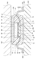
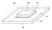
本実施形態のパッケージ実装体は、大きくは、離間して対向する配線基板200および冷却部材300と、配線基板200と冷却部材300との間に介在し、これら両者に結合された半導体パッケージ100と、を備えて構成されている。
The package mounting body of the present embodiment is roughly divided into a
配線基板200は、半導体パッケージ100を搭載する一面201を有し、半導体パッケージ100と電気的なやり取りが行える配線基材であればよい。具体的に、配線基板200としては、典型的なプリント配線基板やセラミック配線基板、あるいは、各種の配線部品等が挙げられる。そして、半導体パッケージ100は、配線基板200の一面201上に搭載されている。
The
一方、冷却部材300は、配線基板200の一面201に対して離間して対向するように配置され、半導体パッケージ100は、配線基板200の一面201と冷却部材300との間に介在されている。この冷却部材300としては、たとえば、半導体パッケージ100および配線基板200を収容するAl等の金属よりなるケース等が挙げられる。
On the other hand, the
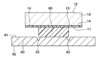
半導体パッケージ100は、大きくは、半導体素子10、金属製のアイランド20、リード端子30、露出部材40、および、これらを封止するモールド樹脂50を備えて構成されたものである。
The
半導体素子10は、表裏の主面のうちの一方を一面11、他方を他面12とする板状をなすものである。そして、モールド樹脂50内に配置された半導体素子10において、半導体素子10の一面11が配線基板200の一面201に対向しつつ、半導体素子10の他面12が冷却部材300に対向している。
The
このような半導体素子10は、シリコン半導体等の半導体材料よりなり、通常の半導体プロセスにより形成されたものである。そして、半導体素子10は、典型的には矩形板状をなすものであり、たとえばマイコン、制御素子、パワー素子等により構成されるものである。
Such a
ここでは、半導体素子10は、ASIC(特定用途向け集積回路、ASICは、application specific integrated circuitの略)である。具体的には、半導体素子10の一面11は、電気絶縁性の保護膜13により構成され、半導体素子10の一面11において、ワイヤパッド14は保護膜13より露出している。
Here, the
ここで、保護膜13は、たとえばポリイミドやポリアミドあるいは窒化シリコン等の絶縁材料を用いた絶縁膜よりなり、ワイヤパッド14は、Al等の導電性材料よりなるものである。
Here, the
アイランド20は、モールド樹脂50内にて、半導体素子10の他面12側に設けられ半導体素子10に接続されている。ここでは、アイランド20は、リード端子30と同一のリードフレーム素材より形成されたアイランドとしている。なお、アイランド20としては、リード端子30とは別体の素材としてのCuやFe等よりなるヒートシンク等であってもよい。
The
このようなアイランド20は、半導体素子10を搭載する素子搭載部としての役目を有する。そして、アイランド20は、通常、金属製の板状をなすものであるが、典型的には半導体素子10よりも大きい矩形板状をなす。ここでは、アイランド20における表裏の板面のうち半導体素子10側の面を一面21とし、半導体素子10とは反対側の面を他面22としている。
Such an
そして、半導体素子10の他面12にて、半導体素子10とアイランド20の一面21とは、ダイボンド材60を介して接合され、固定されている。ここで、ダイボンド材60は、たとえばAgペーストやはんだ等よりなる。
Then, on the
リード端子30は、この種の半導体パッケージと同様、半導体パッケージ100に対して複数設けられている。リード端子30の典型的な配置や形状は、たとえばSOP(スモール・アウトライン・パッケージ)やQFP(クワッド・フラット・パッケージ)等と同様のものにできる。それぞれのリード端子30は、モールド樹脂50内にて、半導体素子10の外側に設けられ、半導体素子10と電気的に接続されている。
Similar to this type of semiconductor package, a plurality of
ここでは、半導体素子10の一面11におけるワイヤパッド14とリード端子30とが、ボンディングワイヤ70により接続されている。このボンディングワイヤ70は、Au、Cu、Ag、Alおよびこれらの合金よりなる。
Here, the
また、ここでは、リード端子30は、上述したようにアイランド20と複数のリード端子30とがタイバー等により一体に連結された典型的なリードフレーム素材を用いて形成されたものである。そして、アイランド20およびリード端子30ともに、たとえばCuや42アロイ等の導電性金属よりなる。リード端子30のそれぞれは、典型的には、細長の板状をなしている。
Here, the
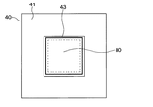
また、半導体パッケージ10において、露出部材40は、モールド樹脂50内にて半導体素子10の一面11側に設けられている。この露出部材40は、具体的には板状、たとえば矩形板状をなすものであり、熱伝導性に優れる材料、たとえばCu等の金属やシリコン、あるいはセラミック等よりなる。ここでは、露出部材40における表裏の板面のうち、半導体素子10側の面を一面41とし、半導体素子10とは反対側の面を他面42としている。
In the
ここで、本実施形態では、モールド樹脂50の内部にて半導体素子10の一面11側には、樹脂よりなる接続部材80が設けられている。接続部材80は、半導体素子10の一面11と露出部材40の一面41との両面間に介在し、これら両面間を接続するものとされている。
Here, in the present embodiment, a
ここで、本実施形態では、露出部材40は接続部材80よりも平面サイズが大きいものとしている。つまり、露出部材40のうち接続部材80との接続面である一面41は、接続部材80の配置面積よりも大きい面積とされている。
Here, in this embodiment, the exposed
この接続部材80を構成する樹脂としては、電気絶縁性は特に問わないが、熱伝導性に優れる樹脂、たとえばポリイミドやエポキシ樹脂等が好ましい。更には、当該樹脂としては、樹脂にアルミナ、シリカ等のセラミック、あるいは、Ag等の金属よりなる熱伝導性に優れたフィラー等が含有されたものであってもよい。本実施形態では、接続部材80として、このような樹脂をフィルム状に成形してなるDAF(ダイ・アタッチ・フィルム)を用いている。
The resin constituting the connecting
また、接続部材80についてさらに言うならば、接続部材80は樹脂より構成されることにより、金属やシリコン等よりなる露出部材40よりも低い弾性率を有するものである。たとえば、露出部材40の弾性率は、接続部材80の弾性率の100倍以上のものとなる。さらには、弾性率の関係としては、接続部材80、モールド樹脂50、露出部材40の順に大きくなっていることが望ましい。
Further, the
また、接続部材80は樹脂よりなるが、加熱により弾性率が低下するもの、具体的には、モールド樹脂50の成形時の加熱により弾性率が低下する樹脂よりなるものであることが望ましい。
The
このような接続部材80の樹脂としては、Tg(ガラス転移点)がモールド樹脂50の成形温度よりも低いものが採用される。限定するものではないが、たとえば、モールド樹脂50の成形温度が175℃とされる場合、接続部材80の樹脂のTgは、100℃程度とされる。
As the resin of the connecting
そして、図1に示されるように、モールド樹脂50は、半導体素子10、アイランド20、リード端子30、露出部材40、ボンディングワイヤ70、接続部材80を封止して一体化している。
As shown in FIG. 1, the
モールド樹脂50は、この種の半導体パッケージに用いられる通常のモールド材料よりなるもので、たとえばエポキシ樹脂等の熱硬化性樹脂よりなる。このようなモールド樹脂50は、トランスファー成形、コンプレッション成形、ディスペンス法、ポッティング法等の通常の樹脂成形方法により形成されるものである。また、限定するものではないが、たとえばエポキシ樹脂の場合、その成形温度は175℃程度である。
The
このような封止形態を有する本実施形態の半導体パッケージにおいて、次のような各部の露出構成が採用されている。それぞれのリード端子30は、モールド樹脂50内に位置するインナーリード部31と、モールド樹脂より突出するアウターリード部32とよりなる。そして、インナーリード部31にて半導体素子10とのボンディングワイヤ70による電気的接続がなされている。
In the semiconductor package of the present embodiment having such a sealing form, the following exposed structure of each part is adopted. Each
一方、アウターリード部32は、典型的なものと同様、リード成形により曲げ加工されることで、モールド樹脂50より配線基板200の一面201に向かって突出している。そしてアウターリード部32は、はんだや導電性接着剤等の接合材202により配線基板200の一面201に機械的および電気的に接続されている。
On the other hand, the
なお、アウターリード部32と配線基板200との接続部において、配線基板200の一面201には図示しない配線や電極等の導電性部材が設けられている。そして、アウターリード部32は、この導電性部材に対して、はんだや導電性接着剤等よりなる接合材202を介して、電気的および機械的に接続されている。
Note that, in a connection portion between the
また、図1に示されるように、アイランド20のうち半導体素子10とは反対側の面である他面22は、モールド樹脂50より露出する露出面とされている。そして、この露出面であるアイランドの他面22において、半導体素子10の熱が放熱されるようになっている。
Further, as shown in FIG. 1, the
本実施形態では、アイランド20の他面22は、モールド樹脂50より露出して、冷却部材300に熱的に接続されている。具体的には、アイランド20の他面22と冷却部材300とは、シリコーングリス等の熱伝導性に優れた熱伝導部材301を介して接触することで、熱的に接続されている。なお、この熱的接続が十分に確保されるならば、熱伝導部材301を省略して、アイランド20の他面22と冷却部材300とは、直接接触するようにしてもよい。
In the present embodiment, the
また、本実施形態では、図1に示されるように、露出部材40のうち半導体素子10とは反対側の面である他面42は、モールド樹脂50より露出して、配線基板200の一面201に機械的に接続されている。
In the present embodiment, as shown in FIG. 1, the
具体的には、露出部材40と配線基板200とは、アウターリード部32と配線基板200との接続部と同様、接合材202を介して機械的に接続されている。この場合も、露出部材40との接続部に位置する配線基板200の一面201には、図示しないが、接合材202との良好な接合性を実現するための金属部材等が設けられていてもよい。
Specifically, the exposed
次に、図2〜図6を参照して、本実施形態にかかる半導体パッケージ100の製造方法の一具体例を示しておく。
Next, a specific example of the method for manufacturing the
まず、図2に示される素子搭載工程を行う。この工程では、アイランド20と複数のリード端子30とが一体に連結されたリードフレーム素材を用意する。そして、アイランド20の一面21に半導体素子10の他面12を対向させ、ダイボンド材60を介して、半導体素子10をアイランド20の一面21に搭載する。
First, the element mounting process shown in FIG. 2 is performed. In this step, a lead frame material in which the
次に、図3に示されるワイヤボンディング工程を行う。この工程では、半導体素子10の一面11におけるワイヤパッド14とリード端子30との間でワイヤボンディングを行い、これらの間を結線するボンディングワイヤ70を形成する。
Next, the wire bonding step shown in FIG. 3 is performed. In this step, wire bonding is performed between the
次に、図4に示される露出部材40の配置工程を行う。この配置工程では、露出部材40の一面41に接続部材80を貼り合わせたものを用意し、このものを、接続部材80を介して半導体素子10の一面11に貼り合わせて接着する。もしくは、半導体素子10の一面11に予め接続部材80を貼り合わせておき、その後、接続部材80に対して露出部材40を貼り付けて接着する。こうして、図4に示されるような樹脂封止前のワークができあがる。
Next, the arrangement process of the exposed
次に、このワークについて、図5に示されるモールド工程を行う。この工程では、上記したトランスファー成形等の樹脂成形方法により、モールド樹脂50による上記ワークの封止を行う。この封止後には、リード端子30のアウターリード部32、アイランド20の他面22および露出部材40の他面42は、モールド樹脂50より露出しており、上述した露出構成を有する封止形態とされている。
Next, the molding process shown in FIG. 5 is performed on the workpiece. In this step, the work is sealed with the
その後、必要に応じて、モールド樹脂50の外部にて、上記したリードフレーム素材におけるタイバー等をカットするリードカットを行う。そして、図6に示されるリード成形工程では、リード端子30のアウターリード部32を、曲げ加工等により所望の形状に成形する。こうして、半導体パッケージ100ができあがる。
Thereafter, if necessary, lead cutting for cutting the tie bars and the like in the lead frame material described above is performed outside the
そして、この半導体パッケージ100は、たとえば、接合材202を介して、配線基板200の一面201に搭載され、接続された後に、配線基板200とともに、ケースとしての冷却部材300に組み付けられる。
Then, for example, the
この冷却部材300への組み付け時に、半導体パッケージ100におけるアイランド20の他面22と冷却部材300との熱的な接続がなされる。こうして、上記図1に示される本実施形態のパッケージ実装体ができあがる。
During the assembly to the cooling
ところで、本実施形態の半導体パッケージ100によれば、配線基板200の一面201に対して、アウターリード部32による機械的接続に加えて、さらに露出部材40による機械的接続がなされている。
By the way, according to the
つまり、半導体パッケージ100と配線基板200の一面201との機械的接続について露出部材40による補強がなされることになるため、リード端子30のアウターリード部32と配線基板200との接続部でのダメージが低減される。
That is, since the exposed
よって、本実施形態のパッケージ実装体によれば、半導体パッケージ100と配線基板200との間における接続信頼性を向上させることができる。さらに、本実施形態によれば、アイランド20から冷却部材300への放熱に加えて、露出部材40から配線基板200への放熱も期待することができる。
Therefore, according to the package package of this embodiment, the connection reliability between the
つまり、半導体素子10の熱は、半導体素子10の一面11からは、接続部材80、露出部材40を介して配線基板200へ放熱され、半導体素子10の他面12からは、アイランド20を介して冷却部材300へ放熱される。そのため、本実施形態によれば、露出部材40の存在により、半導体素子10の一面11および他面12からの両面放熱における放熱性の向上が期待できる。
That is, the heat of the
また、本実施形態のように冷却部材300が設けられている場合、アイランド20の他面22から冷却部材300に放熱することで、アイランド20側における放熱性の更なる向上が期待できる。
Further, when the cooling
なお、本実施形態において、冷却部材300を設けずにアイランド20の他面22を大気に露出させた構成とし、大気への放熱を行うようにしてもよいことはもちろんである。つまり、パッケージ実装体としては、冷却部材300が省略されたものでもよく、少なくとも半導体パッケージ100と、半導体パッケージ100が接続される配線基板200とを備えたものであればよい。
In the present embodiment, it is a matter of course that the
また、本実施形態では、モールド樹脂50の内部にて、半導体素子10の一面11と露出部材40の一面41との間には、半導体素子10と露出部材40とを接続する接続部材80が、介在されている。
Further, in the present embodiment, the
これによれば、モールド樹脂50で封止する前のワーク(図4参照)を、半導体素子10と露出部材40とが接続部材80によって固定されたものにできるため、半導体素子10の両面に組み付けられたアイランド20と露出部材40との間で平行度を出しやすい。具体的に、この平行度は、アイランド20の他面22と露出部材40の他面42との平行度である。
According to this, since the work (see FIG. 4) before sealing with the
ここで、接続部材80が硬いと、たとえば露出部材40が傾いて組み付けられた場合、接続部材80を変形させることによって当該傾きを吸収させることが行いにくい。しかし、本実施形態では、接続部材80は樹脂よりなるので、変形しやすく、上記の平行度を出しやすい。具体的には、接続部材80が厚さ方向(図1の上下方向)に変形することで、上記の傾きの吸収が行われる。
Here, if the connecting
また、上述したが、本実施形態では、接続部材80を露出部材40よりも低い弾性率を有するものとしている。このような低弾性率の接続部材80とすれば、上記した傾きを接続部材80の変形により吸収しやすくなり、上記した平行度に優れたパッケージを実現しやすい。
Further, as described above, in the present embodiment, the
(第2実施形態)
本発明の第2実施形態にかかるパッケージ実装体について、上記第1実施形態との相違点を中心に述べることとする。
(Second Embodiment)
The package mounting body according to the second embodiment of the present invention will be described focusing on the differences from the first embodiment.
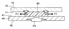
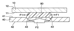
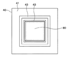
図7、図8に示されるように、本実施形態においても、露出部材40において接続部材80との接続面である一面41は、接続部材80の配置面積よりも大きいものである。そして、本実施形態では、この露出部材40の一面41のうち接続部材80の外周端部に対応する部位に、溝43が設けられている。
As shown in FIGS. 7 and 8, also in the present embodiment, the one
ここでは、溝43は、断面V字形状であり、その配置パターンについては、接続部材80の外周端部の全周に対して設けられている。つまり、図7、図8の例では、溝43の平面形状は矩形の枠状とされている。また、図7、図8に示されるように、溝43全体が、接続部材80の外周端部の外側に位置している。つまり、矩形枠状の溝43の内周領域に接続部材80の外周端部が位置している。
Here, the
このような溝43は、露出部材40の一面41に対して、レーザ照射や切削加工、あるいはエッチング加工等を行うことにより形成される。このように、本第2実施形態は、上記第1実施形態に対して溝43を追加した構成を採用するものであり、それによる効果は、次の通りである。
Such a
上述したが、上記第1実施形態によれば、上記図4に示されるアイランド20と露出部材40との組み付け時に発生する当該両部材間の傾きを、接続部材80が変形することで吸収することができる。
As described above, according to the first embodiment, the connecting
しかしながら、溝43が無い構成の場合、図9に示されるように、接続部材80に大きなせん断応力F1が発生する。これは、モールド工程前のアイランド20と露出部材40との組み付け時に印加される押力F2により、接続部材80が変形して発生するものである。このせん断応力F1が大きいと、接続部材80に接触している半導体素子10へダメージを与えるおそれがある。
However, in the case of the configuration without the
これに対して、本実施形態によれば、図10に示されるように、押力F2により変形した接続部材80の外周端部が溝43に入り込むことで、接続部材80の変形が溝43で吸収される。これにより、本実施形態では、上記の接続部材80に発生するせん断応力F1が低減され、半導体素子10へのダメージが低減されやすいものとなる。
On the other hand, according to the present embodiment, as shown in FIG. 10, the outer peripheral end portion of the
また、本実施形態の半導体パッケージ100の製造方法、および、パッケージ実装体の組み付け方法については、溝43が形成された露出部材40を用いること以外は、上記第1実施形態と同様の方法を採用すればよい。
The manufacturing method of the
なお、露出部材40の配置工程において、先に露出部材40に接続部材80を貼り合わせておき、これを半導体素子10の一面11に貼り合わせる場合、基本的には、露出部材40に溝43を形成した後、露出部材40に接続部材80を貼り合わせればよい。
In the step of arranging the exposed
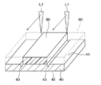
しかし、上記図7、図8に示される例のように、溝43全体が接続部材80の外周端部より外側に位置するときは、溝43の形成前に接続部材80を露出部材40に貼り合わせる方法を採用してもよい。この方法は、図11、図12に示される。
However, when the
この方法では、まず、露出部材40の一面41のうち最終的な接続部材80の配置領域および当該配置領域の外側の領域まで、接続部材80を貼り合わせる。あるいは、露出部材40の一面41の全面に接続部材80を貼り合わせてもよい。
In this method, first, the
その後、図11に示されるように、レーザL1を照射して、接続部材80を切断加工し、不要部分を除去することにより、接続部材80を所望の平面形状にパターニングする。このとき、接続部材80の切断部においては、レーザL1の照射により、露出部材40の一面41が削られて溝43が形成される。
Thereafter, as shown in FIG. 11, the
こうして、図12に示されるように、露出部材40の一面41において、接続部材80が貼り合わせられるとともに、接続部材80の外周端部の位置に溝43が形成される。なお、この手法は、上記したレーザL1に限定されるものではなく、たとえば刃具を用いた切削加工によっても実行できることは、もちろんである。
Thus, as shown in FIG. 12, the
次に、本第2実施形態の他の例について述べておく。図13、図14に示される第1の他の例では、接続部材80の外周端部が、溝43の開口部上に位置している。つまり、溝43のうち内周側の部分は、接続部材80の直下すなわち接続部材80の外周端部よりも内側に位置し、溝43のうち外周側の部分は、接続部材80の外周端部よりも外側に位置している。
Next, another example of the second embodiment will be described. In the first other example shown in FIGS. 13 and 14, the outer peripheral end of the
このように、溝43の一部が接続部材80の外周端部よりも内側に位置するときは、上記図11および図12に示した方法は採用できないので、溝43の形成後に接続部材80を露出部材40に貼り合わせる方法を採用する。そして、本例によっても、上記同様、せん断応力F1の低減による半導体素子10へのダメージ低減の効果が期待できる。
Thus, when a part of the
なお、上記図9および図10に示したように、変形する接続部材80の外周端部が溝43に入り込むことにより、上記効果が発揮されるものである。そのため、接続部材80の外周端部の入り込みを実現するべく、溝43としては、幅方向の一部または全部が、接続部材80の外周端部よりも外側に位置するものであることが望ましい。
As shown in FIGS. 9 and 10, the outer peripheral end portion of the connecting
また、図15、図16に示される第2の例では、上記第1の例において、さらに、もう一つの溝43を外側に設けたものである。つまり、図示例では、露出部材40の他面42のうち接続部材80の外周端部に対応する部位に、2個の連続環状の溝43が、同心の四角形の配置となるように設けられている。
Further, in the second example shown in FIGS. 15 and 16, another
本実施形態では、この第2の例のように、溝43を、2個あるいは3個以上というように複数個設けてもよく、この場合にも、上記同様、せん断応力F1の低減による半導体素子10へのダメージ低減の効果が期待できる。
In the present embodiment, as in the second example, a plurality of
(他の実施形態)
なお、上記各実施形態では、ダイボンド材60として、上記Agペーストやはんだ等、塗布されて配置されるものを用いて、半導体素子10とアイランド20とを固定した。しかし、ダイボンド材60としては、これに限定されるものではなく、たとえば、上記した接続部材80に用いたDAFを用いてもよい。
(Other embodiments)
In each of the above embodiments, the
また、半導体素子10とリード端子30との電気的接続は、上記したボンディングワイヤ70に限定されるものではなく、たとえばリボン等でもよい。あるいは、リード端子30をワイヤパッド14まで延長したものとし、リード端子30とワイヤパッド14とをはんだや金属接合等により直接接合してもよい。
Further, the electrical connection between the
また、露出部材40としては、接続部材80よりも平面サイズが大きいものに限定するものではない。たとえば、上記第2実施形態に示したような溝43を設けない場合には、露出部材40を接続部材80よりも平面サイズが小さいものとしてもよい。つまり、露出部材40の一面41を、接続部材80の配置面積よりも小さいものとしてもよい。あるいは、露出部材40と接続部材80との平面サイズが同等であってもよい。
Further, the exposed
また、露出部材40としては、1個の半導体パッケージ100に複数個設けられていてもよい。この場合、たとえば複数個の露出部材40を、モールド樹脂50内にて平面的に配置し、それぞれの露出部材40の他面42が配線基板200の一面201に対向するようにモールド樹脂50より露出しているものとすればよい。
A plurality of exposed
また、接続部材80としては、上記したDAFのような樹脂をフィルム状に成形してなるものに限定されるものではなく、樹脂を塗布することにより形成された層であってもよい。
Further, the connecting
また、上記各実施形態では、リード端子30のアウターリード部32と配線基板200との接続については、電気的、機械的接続を実現するために、はんだや導電性接着剤等よりなる接合材202が用いられた。しかし、露出部材40と配線基板200との接続については、少なくとも機械的接続が確保されればよいので、接合材202としては、導電性を持たない接着剤等を用いてもよい。
Further, in each of the above embodiments, the connection between the
また、上記各実施形態では、モールド樹脂50の内部にて半導体素子10の一面11と露出部材40との間に、これら両者を接続する接続部材80を介在させたが、この接続部材80は省略された構成であってもよい。この場合、モールド樹脂50の内部にて、半導体素子10の一面11と露出部材40とは離れ、且つ、これら両者間はモールド樹脂50で充填された構成となる。
Further, in each of the above embodiments, the connecting
また、上記第2実施形態では、溝43は断面V字形状であり、接続部材80の外周端部の全周に対して設けられた連続環状のものとされていたが、溝43の断面形状、配置パターンは、これに限定されるものではない。たとえば、溝43は、断面U字、あるいは、断面矩形等の形状でもよい。また、溝43は、接続部材80の外周端部にて断続的に位置するもの、すなわち、不連続形状のものであってもよい。
In the second embodiment, the
さらに、上記第2実施形態において、溝43は、接続部材80の外周端部に対応して設けられるので、たとえば接続部材80が平面円形や平面多角形をなすものであり、溝43を全周に設ける場合には、溝43は円形状や多角形状の配置パターンとされる。
Furthermore, in the said 2nd Embodiment, since the groove |
また、モールド樹脂50内において半導体素子10は、1個に限定されるものではなく、複数個設けられていてもよい。たとえば、アイランド20の一面21に複数個の半導体素子10を設け、それぞれの半導体素子10に対して独立して接続部材80および露出部材40を設ければよい。あるいは、接続部材80および露出部材40は、複数個の半導体素子10に共通するものとしてもよい。
Further, the number of
また、本発明は上記した実施形態に限定されるものではなく、特許請求の範囲に記載した範囲内において適宜変更が可能である。また、上記各実施形態は、互いに無関係なものではなく、組み合わせが明らかに不可な場合を除き、適宜組み合わせが可能であり、また、上記各実施形態は、上記の図示例に限定されるものではない。 Further, the present invention is not limited to the above-described embodiment, and can be appropriately changed within the scope described in the claims. The above embodiments are not irrelevant to each other, and can be combined as appropriate unless the combination is clearly impossible, and the above embodiments are not limited to the illustrated examples. Absent.
10 半導体素子
11 半導体素子の一面
12 半導体素子の他面
20 アイランド
22 アイランドの他面
30 リード端子
32 リード端子のアウターリード部
40 露出部材
42 露出部材の他面
50 モールド樹脂
100 半導体パッケージ
200 配線基板
DESCRIPTION OF
Claims (5)
前記半導体パッケージは、
表裏の主面のうちの一方を一面(11)、他方を他面(12)とし、当該一面が前記配線基板の一面に対向するように配置された半導体素子(10)と、
前記半導体素子の他面側に設けられ前記半導体素子に接続された金属製のアイランド(20)と、
前記半導体素子の外側に設けられ前記半導体素子と電気的に接続された複数のリード端子(30)と、
前記半導体素子の一面側に設けられた露出部材(40)と、
前記半導体素子、前記アイランド、前記リード端子および前記露出部材を封止して一体化するモールド樹脂(50)と、を有するものであり、
前記リード端子の一部は、前記モールド樹脂より前記配線基板の一面に向かって突出するアウターリード部(32)とされ、当該アウターリード部は前記配線基板の一面に機械的および電気的に接続されており、
前記アイランドのうち前記半導体素子とは反対側の面(22)は前記モールド樹脂より露出することで、前記半導体素子の熱を放熱するようになっており、
前記露出部材のうち前記半導体素子とは反対側の面(42)は、前記モールド樹脂より露出して、前記配線基板の一面に機械的に接続されていることを特徴とするパッケージ実装体。 A package mounting body comprising a wiring substrate (200) and a semiconductor package (100) mounted on one surface (201) of the wiring substrate,
The semiconductor package is:
One of the main surfaces of the front and back surfaces is one surface (11), the other is the other surface (12), and the semiconductor element (10) disposed so that the one surface faces one surface of the wiring board;
A metal island (20) provided on the other side of the semiconductor element and connected to the semiconductor element;
A plurality of lead terminals (30) provided outside the semiconductor element and electrically connected to the semiconductor element;
An exposed member (40) provided on one side of the semiconductor element;
A mold resin (50) for sealing and integrating the semiconductor element, the island, the lead terminal and the exposed member;
A part of the lead terminal is an outer lead portion (32) protruding from the mold resin toward one surface of the wiring substrate, and the outer lead portion is mechanically and electrically connected to one surface of the wiring substrate. And
The surface (22) on the opposite side of the island from the island is exposed from the mold resin, so that the heat of the semiconductor element is dissipated,
The package mounting body, wherein a surface (42) of the exposed member opposite to the semiconductor element is exposed from the mold resin and mechanically connected to one surface of the wiring board.
当該接続面のうち前記接続部材の外周端部に対応する部位には、溝(43)が設けられていることを特徴とする請求項1または2に記載のパッケージ実装体。 Of the exposed member, the connection surface (41) with the connection member is larger than the arrangement area of the connection member,
The package mounting body according to claim 1 or 2, wherein a groove (43) is provided in a portion of the connection surface corresponding to the outer peripheral end of the connection member.
前記半導体パッケージは、前記配線基板および前記冷却部材の間に介在されており、
前記アイランドのうち前記半導体素子とは反対側の面は、前記モールド樹脂より露出して、前記冷却部材に熱的に接続されていることを特徴とする請求項1ないし4のいずれか1つに記載のパッケージ実装体。 A cooling member (300) disposed so as to be opposed to and spaced from one surface of the wiring board;
The semiconductor package is interposed between the wiring board and the cooling member,
The surface of the island opposite to the semiconductor element is exposed from the mold resin and is thermally connected to the cooling member. The package package described.
Priority Applications (1)
| Application Number | Priority Date | Filing Date | Title |
|---|---|---|---|
| JP2015146070A JP2017028131A (en) | 2015-07-23 | 2015-07-23 | Package mounting body |
Applications Claiming Priority (1)
| Application Number | Priority Date | Filing Date | Title |
|---|---|---|---|
| JP2015146070A JP2017028131A (en) | 2015-07-23 | 2015-07-23 | Package mounting body |
Publications (1)
| Publication Number | Publication Date |
|---|---|
| JP2017028131A true JP2017028131A (en) | 2017-02-02 |
Family
ID=57946565
Family Applications (1)
| Application Number | Title | Priority Date | Filing Date |
|---|---|---|---|
| JP2015146070A Pending JP2017028131A (en) | 2015-07-23 | 2015-07-23 | Package mounting body |
Country Status (1)
| Country | Link |
|---|---|
| JP (1) | JP2017028131A (en) |
Cited By (2)
| Publication number | Priority date | Publication date | Assignee | Title |
|---|---|---|---|---|
| US10720382B2 (en) | 2017-11-29 | 2020-07-21 | Samsung Electronics Co., Ltd. | Semiconductor package structure and semiconductor module including the same |
| WO2023112709A1 (en) * | 2021-12-14 | 2023-06-22 | オムロン株式会社 | Mounting board, and electric apparatus equipped with mounting board |
Citations (3)
| Publication number | Priority date | Publication date | Assignee | Title |
|---|---|---|---|---|
| JPS58182256A (en) * | 1982-04-16 | 1983-10-25 | Matsushita Electric Ind Co Ltd | Manufacture of semiconductor device |
| JP2003297994A (en) * | 2002-03-29 | 2003-10-17 | Hitachi Ltd | Semiconductor device and manufacturing method thereof |
| JP2005057125A (en) * | 2003-08-06 | 2005-03-03 | Rohm Co Ltd | Semiconductor device |
-
2015
- 2015-07-23 JP JP2015146070A patent/JP2017028131A/en active Pending
Patent Citations (3)
| Publication number | Priority date | Publication date | Assignee | Title |
|---|---|---|---|---|
| JPS58182256A (en) * | 1982-04-16 | 1983-10-25 | Matsushita Electric Ind Co Ltd | Manufacture of semiconductor device |
| JP2003297994A (en) * | 2002-03-29 | 2003-10-17 | Hitachi Ltd | Semiconductor device and manufacturing method thereof |
| JP2005057125A (en) * | 2003-08-06 | 2005-03-03 | Rohm Co Ltd | Semiconductor device |
Cited By (3)
| Publication number | Priority date | Publication date | Assignee | Title |
|---|---|---|---|---|
| US10720382B2 (en) | 2017-11-29 | 2020-07-21 | Samsung Electronics Co., Ltd. | Semiconductor package structure and semiconductor module including the same |
| US11848255B2 (en) | 2017-11-29 | 2023-12-19 | Samsung Electronics Co., Ltd. | Semiconductor package structure on a PCB and semiconductor module including the same |
| WO2023112709A1 (en) * | 2021-12-14 | 2023-06-22 | オムロン株式会社 | Mounting board, and electric apparatus equipped with mounting board |
Similar Documents
| Publication | Publication Date | Title |
|---|---|---|
| JP2020065086A (en) | Semiconductor device | |
| TWI404177B (en) | Electric power semiconductor circuit device and method for making same | |
| JP4438489B2 (en) | Semiconductor device | |
| JP5279632B2 (en) | Semiconductor module | |
| JP6065973B2 (en) | Semiconductor module | |
| JP4899481B2 (en) | Manufacturing method of resin-encapsulated semiconductor device having a heat radiator exposed outside | |
| JP5213884B2 (en) | Semiconductor device module | |
| JP2008141140A (en) | Semiconductor device | |
| JP5262983B2 (en) | Mold package and manufacturing method thereof | |
| JP5169964B2 (en) | Mold package mounting structure and mounting method | |
| JP6048238B2 (en) | Electronic equipment | |
| WO2011083703A1 (en) | Led module device and method for manufacturing same | |
| JP6150866B2 (en) | Power semiconductor device | |
| WO2019038876A1 (en) | Semiconductor device | |
| JP2009283656A (en) | Semiconductor device and manufacturing method thereof | |
| JP2017028131A (en) | Package mounting body | |
| JP2013258354A (en) | Mold package and manufacturing method of the same | |
| JP6048893B2 (en) | Resin package | |
| JP4556732B2 (en) | Semiconductor device and manufacturing method thereof | |
| JP2009206406A (en) | Power semiconductor device | |
| JP2006286679A (en) | Semiconductor device and method of manufacturing it | |
| JP2007150044A (en) | Semiconductor device | |
| JP5987665B2 (en) | Semiconductor device | |
| JP4258391B2 (en) | Semiconductor device | |
| JP2005327791A (en) | Semiconductor device and its packaging structure |
Legal Events
| Date | Code | Title | Description |
|---|---|---|---|
| A621 | Written request for application examination |
Free format text: JAPANESE INTERMEDIATE CODE: A621 Effective date: 20171102 |
|
| A977 | Report on retrieval |
Free format text: JAPANESE INTERMEDIATE CODE: A971007 Effective date: 20180621 |
|
| A02 | Decision of refusal |
Free format text: JAPANESE INTERMEDIATE CODE: A02 Effective date: 20190205 |