WO2013051202A1 - 3レベル電力変換回路システム - Google Patents
3レベル電力変換回路システム Download PDFInfo
- Publication number
- WO2013051202A1 WO2013051202A1 PCT/JP2012/005842 JP2012005842W WO2013051202A1 WO 2013051202 A1 WO2013051202 A1 WO 2013051202A1 JP 2012005842 W JP2012005842 W JP 2012005842W WO 2013051202 A1 WO2013051202 A1 WO 2013051202A1
- Authority
- WO
- WIPO (PCT)
- Prior art keywords
- circuit
- semiconductor switch
- series
- switch
- power supply
- Prior art date
- Legal status (The legal status is an assumption and is not a legal conclusion. Google has not performed a legal analysis and makes no representation as to the accuracy of the status listed.)
- Ceased
Links
Images




Classifications
-
- H—ELECTRICITY
- H02—GENERATION; CONVERSION OR DISTRIBUTION OF ELECTRIC POWER
- H02M—APPARATUS FOR CONVERSION BETWEEN AC AND AC, BETWEEN AC AND DC, OR BETWEEN DC AND DC, AND FOR USE WITH MAINS OR SIMILAR POWER SUPPLY SYSTEMS; CONVERSION OF DC OR AC INPUT POWER INTO SURGE OUTPUT POWER; CONTROL OR REGULATION THEREOF
- H02M7/00—Conversion of AC power input into DC power output; Conversion of DC power input into AC power output
- H02M7/42—Conversion of DC power input into AC power output without possibility of reversal
- H02M7/44—Conversion of DC power input into AC power output without possibility of reversal by static converters
- H02M7/48—Conversion of DC power input into AC power output without possibility of reversal by static converters using discharge tubes with control electrode or semiconductor devices with control electrode
- H02M7/483—Converters with outputs that each can have more than two voltages levels
-
- H—ELECTRICITY
- H02—GENERATION; CONVERSION OR DISTRIBUTION OF ELECTRIC POWER
- H02M—APPARATUS FOR CONVERSION BETWEEN AC AND AC, BETWEEN AC AND DC, OR BETWEEN DC AND DC, AND FOR USE WITH MAINS OR SIMILAR POWER SUPPLY SYSTEMS; CONVERSION OF DC OR AC INPUT POWER INTO SURGE OUTPUT POWER; CONTROL OR REGULATION THEREOF
- H02M1/00—Details of apparatus for conversion
- H02M1/32—Means for protecting converters other than automatic disconnection
-
- H—ELECTRICITY
- H02—GENERATION; CONVERSION OR DISTRIBUTION OF ELECTRIC POWER
- H02M—APPARATUS FOR CONVERSION BETWEEN AC AND AC, BETWEEN AC AND DC, OR BETWEEN DC AND DC, AND FOR USE WITH MAINS OR SIMILAR POWER SUPPLY SYSTEMS; CONVERSION OF DC OR AC INPUT POWER INTO SURGE OUTPUT POWER; CONTROL OR REGULATION THEREOF
- H02M7/00—Conversion of AC power input into DC power output; Conversion of DC power input into AC power output
- H02M7/42—Conversion of DC power input into AC power output without possibility of reversal
- H02M7/44—Conversion of DC power input into AC power output without possibility of reversal by static converters
- H02M7/48—Conversion of DC power input into AC power output without possibility of reversal by static converters using discharge tubes with control electrode or semiconductor devices with control electrode
- H02M7/483—Converters with outputs that each can have more than two voltages levels
- H02M7/487—Neutral point clamped inverters
-
- H—ELECTRICITY
- H02—GENERATION; CONVERSION OR DISTRIBUTION OF ELECTRIC POWER
- H02P—CONTROL OR REGULATION OF ELECTRIC MOTORS, ELECTRIC GENERATORS OR DYNAMO-ELECTRIC CONVERTERS; CONTROLLING TRANSFORMERS, REACTORS OR CHOKE COILS
- H02P27/00—Arrangements or methods for the control of AC motors characterised by the kind of supply voltage
- H02P27/04—Arrangements or methods for the control of AC motors characterised by the kind of supply voltage using variable-frequency supply voltage, e.g. inverter or converter supply voltage
- H02P27/06—Arrangements or methods for the control of AC motors characterised by the kind of supply voltage using variable-frequency supply voltage, e.g. inverter or converter supply voltage using DC to AC converters or inverters
- H02P27/08—Arrangements or methods for the control of AC motors characterised by the kind of supply voltage using variable-frequency supply voltage, e.g. inverter or converter supply voltage using DC to AC converters or inverters with pulse width modulation
- H02P27/14—Arrangements or methods for the control of AC motors characterised by the kind of supply voltage using variable-frequency supply voltage, e.g. inverter or converter supply voltage using DC to AC converters or inverters with pulse width modulation with three or more levels of voltage
-
- H—ELECTRICITY
- H02—GENERATION; CONVERSION OR DISTRIBUTION OF ELECTRIC POWER
- H02P—CONTROL OR REGULATION OF ELECTRIC MOTORS, ELECTRIC GENERATORS OR DYNAMO-ELECTRIC CONVERTERS; CONTROLLING TRANSFORMERS, REACTORS OR CHOKE COILS
- H02P29/00—Arrangements for regulating or controlling electric motors, appropriate for both AC and DC motors
- H02P29/02—Providing protection against overload without automatic interruption of supply
- H02P29/024—Detecting a fault condition, e.g. short circuit, locked rotor, open circuit or loss of load
- H02P29/027—Detecting a fault condition, e.g. short circuit, locked rotor, open circuit or loss of load the fault being an over-current
-
- H—ELECTRICITY
- H02—GENERATION; CONVERSION OR DISTRIBUTION OF ELECTRIC POWER
- H02P—CONTROL OR REGULATION OF ELECTRIC MOTORS, ELECTRIC GENERATORS OR DYNAMO-ELECTRIC CONVERTERS; CONTROLLING TRANSFORMERS, REACTORS OR CHOKE COILS
- H02P29/00—Arrangements for regulating or controlling electric motors, appropriate for both AC and DC motors
- H02P29/02—Providing protection against overload without automatic interruption of supply
- H02P29/032—Preventing damage to the motor, e.g. setting individual current limits for different drive conditions
-
- H—ELECTRICITY
- H04—ELECTRIC COMMUNICATION TECHNIQUE
- H04M—TELEPHONIC COMMUNICATION
- H04M1/00—Substation equipment, e.g. for use by subscribers
- H04M1/26—Devices for calling a subscriber
- H04M1/30—Devices which can set up and transmit only one digit at a time
- H04M1/31—Devices which can set up and transmit only one digit at a time by interrupting current to generate trains of pulses; by periodically opening and closing contacts to generate trains of pulses
- H04M1/32—Locking setting devices during transmission to prevent interference by user
-
- H—ELECTRICITY
- H02—GENERATION; CONVERSION OR DISTRIBUTION OF ELECTRIC POWER
- H02M—APPARATUS FOR CONVERSION BETWEEN AC AND AC, BETWEEN AC AND DC, OR BETWEEN DC AND DC, AND FOR USE WITH MAINS OR SIMILAR POWER SUPPLY SYSTEMS; CONVERSION OF DC OR AC INPUT POWER INTO SURGE OUTPUT POWER; CONTROL OR REGULATION THEREOF
- H02M1/00—Details of apparatus for conversion
- H02M1/32—Means for protecting converters other than automatic disconnection
- H02M1/325—Means for protecting converters other than automatic disconnection with means for allowing continuous operation despite a fault, i.e. fault tolerant converters
Definitions
- the present invention relates to a three-level power conversion circuit system for driving an AC motor.
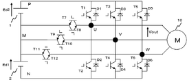
- FIG. 3 shows an example of the circuit configuration of a three-level inverter that converts power from direct current to alternating current.
- the DC power supplies 1 and 2 are connected in series, the positive electrode potential is P, the negative electrode potential is N, and the midpoint potential is M.
- this DC power supply is configured from an AC power supply system, it is possible to configure a rectifier (not shown) and a large capacity electrolytic capacitor in series connection or the like.
- a U-phase series circuit in which an IGBT T1 in which a diode D1 is reverse-parallel connected and an IGBT T2 in which a diode D2 is reverse-parallel connected is connected in series;
- a W-phase series circuit in which an IGBT T5 in which the diode D5 is connected in antiparallel and an IGBT T6 in which the diode D6 is connected in antiparallel are connected in series.
- the three-phase bridge inverter circuit is connected in parallel with the circuit.
- a U-phase bi-directional switch in which reverse blocking IGBTs T7 and T8 are connected anti-parallel to the series connection point U of the U-phase series circuit and the connection point M of the DC power supplies 1 and 2 is a series connection point of the V-phase series circuit.
- a V-phase bidirectional switch in which reverse blocking IGBTs T9 and T10 are connected in antiparallel to the connection point M of V and DC power supplies 1 and 2 is connected between the series connection point W of the W-phase series circuit and DC power supplies 1 and 2
- a W-phase bidirectional switch in which reverse blocking IGBTs T11 and T12 are connected in antiparallel is connected.
- the series connection points U, V, W are connected to the motor 10 which is a load.
- the bidirectional switch can be realized also by a configuration in which an IGBT having no reverse withstand voltage and a diode are combined.
- FIG. 4 shows an example of an output voltage (Vout) waveform. It can output three levels of voltage: DC voltage 0, Ed1, Ed1 + Ed2. This method can construct a high efficiency system because it has less low-order harmonic components and can reduce switching loss of the switch element with respect to the two-level type inverter.
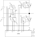
- FIG. 6 shows a system diagram of one phase including a gate drive circuit for driving an IGBT and a control circuit for generating a gate drive signal.
- 11a to 11d are connected between the gate and the emitter of each IGBT in a gate drive circuit, and on / off control of the IGBT is performed by gate drive signals 13a to 13d from the control circuit 12.
- the diodes 14a to 14d are connected for the purpose of detecting the potential of the collector of each IGBT, and detection circuit 15a to 15d in the gate drive circuit causes a short circuit current of the power supply (arm Detect short circuit current). At that time, failure detection signals 16a to 16d are output to the control circuit 12.
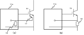
- FIG. 7 shows another method of detecting the arm short circuit current
- FIG. 7 (a) uses the sense IGBT 17 built in the IGBT chip to detect the current value (in fact, the resistor 18 is connected in series and both ends thereof Detect the voltage).
- FIG. 7 (b) shows a method in which a shunt resistor 19 is connected in series with the IGBT to detect a voltage value at both ends thereof. In both methods, detection is performed by detecting an excessive voltage generated across the resistor due to the arm short circuit current.
- an object of the present invention is to provide a small-sized, low-cost system capable of continuing operation even when a semiconductor switch element fails.
- a power conversion circuit that converts power from direct current to alternating current or from alternating current to direct current, and includes two DC power supplies connected in series, and parallel connection with the DC power supply Connected between the series connection point of the semiconductor switch series circuit in which the first and second semiconductor switches in which the respective diodes are reversely connected in series are connected in series and the semiconductor switch series circuit and the series connection point of the DC power supply
- a power conversion circuit capable of outputting three levels of potential using a plurality of switch circuits for one phase consisting of a bidirectional semiconductor switch circuit, a semiconductor switch forming any one of the bidirectional semiconductor switch circuits Or an opening means for electrically opening the path through which the main current of the semiconductor switch or the diode flows in the event of a diode failure, And it turns off the semiconductor switching circuit sex constantly.
- the second invention after failure of the semiconductor switch or the diode forming any one of the bidirectional semiconductor switch circuits in the first invention, a plurality of the semiconductor switch series connected in parallel with the DC power supply is used. In the circuit, the operation is continued as an inverter system of two level output.
- the present invention even if the semiconductor switch or diode constituting the bidirectional semiconductor switch circuit fails, the operation can be continued as an inverter, and it is not necessary to construct a parallel redundant system. As a result, it becomes possible to construct a small and inexpensive power conversion circuit system.
- the present invention is useful for a system such as an uninterruptible power supply (UPS) or an electric vehicle (EV) that requires continuation of the operation even if the semiconductor switch or diode of the bidirectional semiconductor switch circuit fails.
- UPS uninterruptible power supply
- EV electric vehicle
- operation of this invention is shown. It is an example of the driving
- the gist of the present invention is a series connection point of a semiconductor switch series circuit in which two DC power sources connected in series and first and second semiconductor switches connected in parallel with the DC power source are connected in series and the semiconductor switch series circuit.
- a power conversion circuit capable of outputting three levels of potential using a plurality of switch circuits for one phase consisting of a bi-directional semiconductor switch circuit connected between the power supply and the series connection point of the DC power supply.
- the semiconductor switch or the diode is provided with an opening means for electrically opening the path through which the main current of the diode flows, The point is that the semiconductor switch circuit is always turned off and the operation is continued as a two-level inverter.
- the bidirectional semiconductor switch circuit will be described as a bidirectional switch.
- FIG. 1 shows a first embodiment of the present invention. It is an operation
- FIG. 2 is a circuit diagram for explaining the continuous operation operation in the case where the bidirectional switch constituted by the reverse blocking IGBTs T7 and T8 fails.
- the bi-directional switch (anti-parallel connection circuit of T7 and T8) connected between the series connection point of DC power supplies 1 and 2 and the series connection of IGBT T1 and T2 is connected in series
- the mechanical switch 24 and the fuse 25 are connected to each other. It is also required for other two-way switches, but is omitted.
- the main side element which is an element of the semiconductor switch series circuit is not determined to be in arm short circuit state in block 26 during normal operation, and two level operation in block 27 is not performed, At block 28, normal three-level operation is continued.
- the block 23 outputs the signal 23 outputted from the control circuit 12 As a trigger, a mechanical switch 24 forcibly opens electrically so that the failed arm is not energized. Also, as a passive method of electrically opening, if the fuse 25 is connected to each arm in the middle part, the mechanical switch becomes unnecessary (only one phase is shown in the figure, but in fact all three phases are necessary). Further, in the block 31, the control circuit 12 outputs an off command signal to all the semiconductor switches in the middle part which is a bidirectional switch, and in the block 32, the inverter operation is switched to the two level operation using only the main side element.
- the two-level operation is continued as it is. Furthermore, when the arm short circuit detection is performed in block 26 and the two-level operation is further performed in block 29, the system operation is stopped because the continuation of the inverter operation is not possible (block 34). As described above, when a bidirectional switch fails, the broken bidirectional switch is separated by a mechanical switch or a fuse, and the remaining bidirectional switch is supplied with an off signal, and a semiconductor switch series circuit element If the (main element) is sound, the operation is continued as a two-level inverter.
- the main circuit of the two-level inverter is extremely general, and the control method thereof is conventionally implemented by a large number of methods, so the description thereof is omitted in this paper.
- the semiconductor switch element is an IGBT in this embodiment, it can be realized by a MOSFET or a GTO.
- the present invention is also applicable to a multilevel circuit with five or more levels, in which a bidirectional switch circuit is connected to an intermediate potential point of a DC power supply.
- the present invention is a three-level power conversion circuit using a bi-directional switch, which is a proposal of a system that can continue operation as a two-level inverter when an element of the bi-directional switch fails. It is possible to apply to electric vehicles and the like.
Landscapes
- Engineering & Computer Science (AREA)
- Power Engineering (AREA)
- Signal Processing (AREA)
- Inverter Devices (AREA)
Abstract
電力変換回路で、素子故障の場合,運転継続は不可能となるため,故障検知後は半導体スイッチを全オフし,システムを停止する。UPSのような運転継続が必要なシステムでは,インバータを並列接続する並列冗長システムを構築するが、装置の大型化やシステム価格の上昇といった課題を有する。 直列接続された直流電源と、直流電源と並列接続される半導体スイッチ直列回路とその直列接続点と前記直流電源の直列接続点との間に接続される双方向スイッチとからなる1相分のスイッチ回路を複数個用いた3レベル電力変換回路において、双方向スイッチを構成する半導体素子が故障した場合に、前記半導体素子の主電流が流れる経路を電気的に開放する手段を備え、残りの双方向スイッチを常時オフ状態とし、2レベルインバータとして運転を続行させる。
Description
本発明は、交流電動機駆動を目的とした3レベル電力変換回路システムに関する。
図3に、直流から交流に電力変換する3レベルインバータの回路構成例を示す。直流電源1と2が直列に接続され、正極電位をP、負極電位をN、中点電位をMとする。一般に本直流電源を交流電源システムより構成する場合は、図示していない整流器と大容量の電解コンデンサを2直列接続などによって構成することが可能である。
ダイオードD1が逆並列接続されたIGBTT1とダイオードD2が逆並列接続されたIGBTT2とを直列接続したU相用直列回路と、ダイオードD3が逆並列接続されたIGBTT3とダイオードD4が逆並列接続されたIGBTT4とを直列接続したV相用直列回路と、ダイオードD5が逆並列接続されたIGBTT5とダイオードD6が逆並列接続されたIGBTT6とを直列接続したW相用直列回路が、直流電源1と2の直列回路と並列に接続され、3相ブリッジインバータ回路を構成する。
U相用直列回路の直列接続点Uと直流電源1と2の接続点Mには逆阻止形IGBTT7とT8を逆並列接続したU相用双方向スイッチが、V相用直列回路の直列接続点Vと直流電源1と2の接続点Mには逆阻止形IGBTT9とT10を逆並列接続したV相用双方向スイッチが、W相用直列回路の直列接続点Wと直流電源1と2の接続点Mには逆阻止形IGBTT11とT12を逆並列接続したW相用双方向スイッチが、各々接続される。また、直列接続点U、V、Wは負荷である電動機10に接続される。ここで双方向スイッチとしては、図5(b)に示すように、逆耐圧を有しないIGBTとダイオードとを組み合わせた構成でも実現できる。
本回路構成とすることで、電動機10に印加される電位は、P電位、N電位、及びM電位を出力することが可能となるため、3レベル出力のインバータとなる。図4に出力電圧(Vout)波形例を示す。直流電圧0、Ed1、Ed1+Ed2の3つのレベルの電圧を出力できる。本方式は2レベルタイプのインバータに対して、低次の高調波成分が少ないことや、スイッチ素子のスイッチング損失が低減できることから、高効率システムの構築が可能となる。
図6にIGBTを駆動するゲート駆動回路と、ゲート駆動信号を生成する制御回路を含めた1相分のシステム図を示す。11a~11dがゲート駆動回路で各IGBTのゲート・エミッタ間に接続され、制御回路12からのゲート駆動信号13a~13dによってIGBTをオンオフ制御する。また、ダイオード14a~14dは各IGBTのコレクタ部の電位を検出する目的で接続され、ゲート駆動回路内の検出回路15a~15dによって、対応するIGBT又はダイオードが故障したことによって流れる電源短絡電流(アーム短絡電流)の検知を行う。その際、制御回路12へは故障検出信号16a~16dを出力する。
図7はアーム短絡電流を検出する別の方式で、図7(a)がIGBTチップに内蔵のセンスIGBT17を利用し、その電流値を検出する方式(実際は直列に抵抗18を接続してその両端電圧を検出する)である。図7(b)はIGBTと直列にシャント抵抗19を接続してその両端の電圧値を検出する方式である。両方式ともアーム短絡電流によって抵抗の両端に発生した過大な電圧を検出することで検知を行う。
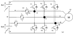
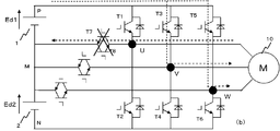
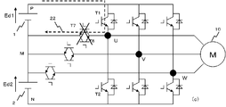
例えば図8(a)の状態(IGBTT3とT5からIGBTT7を介して、電圧Ed1を電動機に供給している状態)で、同図(b)のように中間側素子であるIGBTT7又はT8が故障した時に、同図(c)のようにIGBTT1がターンオンすると、過大な電源短絡電流22が流れる。一般にIGBTは10μs程度は電源短絡電流に対して非破壊保証されているため、正常なIGBTであるT1のゲート駆動回路によって10μs以内に電源短絡電流を検知し、ゲート遮断を行えば、2次被害が発生しない。
即ち、保護動作が行われたゲート駆動回路からの故障検出信号によって、どのアームの半導体素子が故障したかが判る。
以上の3レベルインバータの回路例については、特許文献1に、またIGBTの電源短絡電流保護方式については特許文献2に、各々示されている。
即ち、保護動作が行われたゲート駆動回路からの故障検出信号によって、どのアームの半導体素子が故障したかが判る。
以上の3レベルインバータの回路例については、特許文献1に、またIGBTの電源短絡電流保護方式については特許文献2に、各々示されている。
一般に図3に示すようなインバータシステムでは,半導体スイッチ素子又はダイオードが故障した場合,そのアームは短絡状態又は開放状態となる。いずれの場合も,インバータ運転の継続は不可能であるため,図6に示すような故障検知後はインバータの半導体スイッチを全オフし,システム停止を行う必要があった。
ところが無停電電源装置(UPS)などのような運転継続が必要なシステムでは,インバータを並列接続し,一方のUPSが故障しても,もう一方のUPSにて運転を継続するシステム(待機冗長又は並列冗長システム)を構築している。しかし、このようなシステムでは装置の大型化やシステム価格の上昇といった課題を有する。
従って、本発明の課題は、半導体スイッチ素子が故障しても,小型・低価格で運転継続可能なシステムを提供することである。
ところが無停電電源装置(UPS)などのような運転継続が必要なシステムでは,インバータを並列接続し,一方のUPSが故障しても,もう一方のUPSにて運転を継続するシステム(待機冗長又は並列冗長システム)を構築している。しかし、このようなシステムでは装置の大型化やシステム価格の上昇といった課題を有する。
従って、本発明の課題は、半導体スイッチ素子が故障しても,小型・低価格で運転継続可能なシステムを提供することである。
上述の課題を解決するために、第1の発明においては、直流から交流又は交流から直流に電力変換する電力変換回路であって、2個直列接続された直流電源と、前記直流電源と並列接続されるそれぞれダイオードを逆並列接続した第1及び第2の半導体スイッチを直列接続した半導体スイッチ直列回路と前記半導体スイッチ直列回路の直列接続点と前記直流電源の直列接続点との間に接続される双方向性の半導体スイッチ回路とからなる1相分のスイッチ回路を複数個用いた3レベルの電位が出力可能な電力変換回路において、前記いずれかの双方向性の半導体スイッチ回路を構成する半導体スイッチ又はダイオードが故障した場合に、前記半導体スイッチ又はダイオードの主電流が流れる経路を電気的に開放する開放手段を備え、残りの双方向性の半導体スイッチ回路を常時オフ状態とする。
第2の発明においては、第1の発明におけるいずれかの双方向性の半導体スイッチ回路を構成する半導体スイッチ又はダイオードが故障した後は、前記直流電源と並列に接続される複数の前記半導体スイッチ直列回路にて、2レベル出力のインバータシステムとして運転を継続する。
本発明では、双方向性の半導体スイッチ回路を構成する半導体スイッチ又はダイオードが故障してもインバータとして運転継続が可能となるため、並列冗長システムを構築する必要がなくなる。その結果,小型で低価格の電力変換回路システムの構築が可能となる。
特に、無停電電源装置(UPS)や電気自動車(EV)など,双方向性の半導体スイッチ回路の半導体スイッチ又はダイオードが故障しても運転動作継続が必要なシステムには有用となる。
特に、無停電電源装置(UPS)や電気自動車(EV)など,双方向性の半導体スイッチ回路の半導体スイッチ又はダイオードが故障しても運転動作継続が必要なシステムには有用となる。
本発明の要点は、2個直列接続された直流電源と、前記直流電源と並列接続される第1及び第2の半導体スイッチを直列接続した半導体スイッチ直列回路と前記半導体スイッチ直列回路の直列接続点と前記直流電源の直列接続点との間に接続される双方向性の半導体スイッチ回路とからなる1相分のスイッチ回路を複数個用いた3レベルの電位が出力可能な電力変換回路において、いずれかの双方向性の半導体スイッチ回路を構成する半導体スイッチ又はダイオードが故障した場合に、前記半導体スイッチ又はダイオードの主電流が流れる経路を電気的に開放する開放手段を備え、残りの双方向性の半導体スイッチ回路を常時オフ状態とし、2レベルインバータとして運転を続行させる点である。以下、双方向性の半導体スイッチ回路は双方向スイッチと記載する。
図1に、本発明の第1の実施例を示す。インバータ運転における動作フローチャート図である。図2に、逆阻止形IGBTT7とT8で構成された双方向スイッチが故障した場合の継続運転動作を説明するための回路図を示す。故障した双方向スイッチを開放するために、直流電源1と2の直列接続点とIGBTT1とT2の直列接続点との間に接続された双方向スイッチ(T7とT8の逆並列接続回路)と直列に機械式スイッチ24とヒューズ25を接続する。他の双方向スイッチにも必要であるが、省略してある。
図1の動作フローチャート図において、通常運転中,ブロック26において半導体スイッチ直列回路の素子であるメイン側素子がアーム短絡状態であることが判断されず,かつブロック27で2レベル運転中でない場合は,ブロック28となり,通常の3レベル運転が継続される。
図1の動作フローチャート図において、通常運転中,ブロック26において半導体スイッチ直列回路の素子であるメイン側素子がアーム短絡状態であることが判断されず,かつブロック27で2レベル運転中でない場合は,ブロック28となり,通常の3レベル運転が継続される。
一方,図6に示す信号16(16a~16d)によってアーム短絡状態であることを判断し,かつブロック29で2レベル運転中でない場合は,ブロック30において,制御回路12から出力される信号23をトリガにして,故障したアームに通電が行われないように,機械的なスイッチ24によって強制的に電気的な開放を行う。また、電気的開放を行うパッシブな方法として,中間部の各アームにヒューズ25を接続すれば前記機械的スイッチは不要となる(図では1相分のみを記載しているが,実際は3相とも必要)。さらに、ブロック31では,制御回路12から双方向スイッチである中間部の全ての半導体スイッチに対してオフ指令信号を出力し,ブロック32でインバータ運転をメイン側素子のみによる2レベル運転に切換える。
また、ブロック27で2レベル運転中である時は,そのまま2レベル運転を継続する。
さらに、ブロック26でアーム短絡検知が行われ,さらにブロック29で2レベル運転中であった場合は,インバータ運転の継続は不可であるため,システム停止する(ブロック34)。以上の説明のように、双方向スイッチが故障した場合には、故障した双方向スイッチを機械的スイッチやヒューズなどで切り離し、残りの双方向スイッチにはオフ信号を与え、半導体スイッチ直列回路の素子(メイン素子)が健全であれば、2レベルインバータとして運転を継続する。
さらに、ブロック26でアーム短絡検知が行われ,さらにブロック29で2レベル運転中であった場合は,インバータ運転の継続は不可であるため,システム停止する(ブロック34)。以上の説明のように、双方向スイッチが故障した場合には、故障した双方向スイッチを機械的スイッチやヒューズなどで切り離し、残りの双方向スイッチにはオフ信号を与え、半導体スイッチ直列回路の素子(メイン素子)が健全であれば、2レベルインバータとして運転を継続する。
ところで2レベルインバータの主回路は極一般的であり,その制御方法については,従来から多数の方法で実施されているため,本稿ではその記載を省略する。
尚、本実施例では半導体スイッチ素子をIGBTとしたが,MOSFETやGTOなどでも実現できる。
また本発明は,5レベル以上のマルチレベル回路で,直流電源の中間電位点に双方向性のスイッチ回路が接続される方式においても適用可能である。
尚、本実施例では半導体スイッチ素子をIGBTとしたが,MOSFETやGTOなどでも実現できる。
また本発明は,5レベル以上のマルチレベル回路で,直流電源の中間電位点に双方向性のスイッチ回路が接続される方式においても適用可能である。
本発明は、双方向スイッチを使用した3レベル電力変換回路において、双方向スイッチの素子が故障した場合に、2レベルインバータとして運転継続が可能となるシステムの提案であり、無停電電源装置(UPS)や電気自動車などへの適用が可能である。
1、2・・・直流電源 10・・・電動機
11a~11d・・・ゲート駆動回路 12・・・制御回路
15a~15d・・・検出回路
17・・・センスIGBT
18、19・・・抵抗
T1~T6・・・IGBT
T7~T12・・・逆阻止形IGBT
D1~D6、14a~14d・・・ダイオード
11a~11d・・・ゲート駆動回路 12・・・制御回路
15a~15d・・・検出回路
17・・・センスIGBT
18、19・・・抵抗
T1~T6・・・IGBT
T7~T12・・・逆阻止形IGBT
D1~D6、14a~14d・・・ダイオード
Claims (2)
- 直流から交流又は交流から直流に電力変換する電力変換回路であって、2個直列接続された直流電源と、前記直流電源と並列接続されるそれぞれダイオードを逆並列接続した第1及び第2の半導体スイッチを直列接続した半導体スイッチ直列回路と前記半導体スイッチ直列回路の直列接続点と前記直流電源の直列接続点との間に接続される双方向性の半導体スイッチ回路とからなる1相分のスイッチ回路を複数個用いた3レベルの電位が出力可能な電力変換回路において、前記いずれかの双方向性の半導体スイッチ回路を構成する半導体スイッチ又はダイオードが故障した場合に、前記半導体スイッチ又はダイオードの主電流が流れる経路を電気的に開放する開放手段を備え、残りの双方向性のスイッチ回路を常時オフ状態とすることを特徴とする3レベル電力変換回路システム。
- 前記いずれかの双方向性のスイッチ回路を構成する半導体スイッチ又はダイオードが故障した後は、前記直流電源と並列に接続される複数の前記半導体スイッチ直列回路にて、2レベル出力のインバータシステムとして運転を継続することを特徴とする請求項1に記載の3レベル電力変換回路システム。
Priority Applications (1)
| Application Number | Priority Date | Filing Date | Title |
|---|---|---|---|
| US14/349,866 US9106155B2 (en) | 2011-10-06 | 2012-09-13 | Three-level power conversion circuit system |
Applications Claiming Priority (2)
| Application Number | Priority Date | Filing Date | Title |
|---|---|---|---|
| JP2011221839A JP5849586B2 (ja) | 2011-10-06 | 2011-10-06 | 3レベル電力変換回路システム |
| JP2011-221839 | 2011-10-06 |
Publications (1)
| Publication Number | Publication Date |
|---|---|
| WO2013051202A1 true WO2013051202A1 (ja) | 2013-04-11 |
Family
ID=48043388
Family Applications (1)
| Application Number | Title | Priority Date | Filing Date |
|---|---|---|---|
| PCT/JP2012/005842 Ceased WO2013051202A1 (ja) | 2011-10-06 | 2012-09-13 | 3レベル電力変換回路システム |
Country Status (3)
| Country | Link |
|---|---|
| US (1) | US9106155B2 (ja) |
| JP (1) | JP5849586B2 (ja) |
| WO (1) | WO2013051202A1 (ja) |
Cited By (5)
| Publication number | Priority date | Publication date | Assignee | Title |
|---|---|---|---|---|
| CN103607132A (zh) * | 2013-11-28 | 2014-02-26 | 上海应用技术学院 | 具有容错拓扑的npc三电平逆变器电路及其控制方法 |
| WO2014206374A1 (en) | 2013-06-28 | 2014-12-31 | Shenzhen Byd Auto R & D Company Limited | Charging system for electric vehicle and method for controlling charging of electric vehicle |
| CN104253555A (zh) * | 2013-06-26 | 2014-12-31 | 富士电机株式会社 | 多电平功率转换电路 |
| EP3014734A4 (en) * | 2013-06-28 | 2016-08-10 | Byd Co Ltd | POWER SYSTEM FOR AN ELECTRIC VEHICLE, ELECTRIC VEHICLE AND MOTOR CONTROL |
| CN112671253A (zh) * | 2021-03-15 | 2021-04-16 | 四川华泰电气股份有限公司 | 级联h桥变换器、开路故障冗余处理方法、介质和设备 |
Families Citing this family (24)
| Publication number | Priority date | Publication date | Assignee | Title |
|---|---|---|---|---|
| JP5686103B2 (ja) * | 2012-01-18 | 2015-03-18 | トヨタ自動車株式会社 | 電力変換装置 |
| DE102012016450B4 (de) * | 2012-08-16 | 2015-10-15 | Airbus Defence and Space GmbH | Sende-/Empfangselement für ein aktives, elektronisch gesteuertes Antennensystem |
| WO2014199732A1 (ja) * | 2013-06-14 | 2014-12-18 | 富士電機株式会社 | マルチレベルインバータ |
| JP6086157B2 (ja) * | 2013-10-02 | 2017-03-01 | 富士電機株式会社 | 3レベルインバータ |
| US20150102671A1 (en) * | 2013-10-15 | 2015-04-16 | General Electric Company | Direct current power transmission system |
| EP3128669B1 (en) * | 2014-04-03 | 2020-09-09 | Fuji Electric Co., Ltd. | Safety control device |
| CN103944148A (zh) * | 2014-04-17 | 2014-07-23 | 华为技术有限公司 | 一种t型三电平逆变器的保护方法、装置及逆变电路 |
| CN105226975B (zh) * | 2014-06-06 | 2017-12-15 | 台达电子企业管理(上海)有限公司 | Tnpc逆变器装置及其桥臂短路检测方法 |
| US9825489B2 (en) * | 2015-01-26 | 2017-11-21 | Vertiv S.R.L. | Method of controlling an uninterruptible power supply to clear a shorted load |
| KR102453339B1 (ko) * | 2015-10-30 | 2022-10-11 | 현대모비스 주식회사 | 고장 회피 회로를 가지는 멀티레벨 인버터 |
| US10679949B2 (en) | 2016-03-11 | 2020-06-09 | Mediatek Inc. | Semiconductor package assembly with redistribution layer (RDL) trace |
| DE102016216324A1 (de) * | 2016-08-30 | 2018-03-01 | Robert Bosch Gmbh | Antriebssystem, insbesondere für ein Fahrzeug, und Verfahren zum Aufheizen eines Antriebssystems |
| JP2018107857A (ja) * | 2016-12-22 | 2018-07-05 | 富士電機株式会社 | 電力変換装置 |
| DE102017203065A1 (de) * | 2017-02-24 | 2018-08-30 | Volkswagen Aktiengesellschaft | Antriebsumrichter mit integriertem boost-converter |
| US20200406769A1 (en) | 2018-03-12 | 2020-12-31 | Jabil Inc. | Multilevel motor drive with integrated battery charger |
| JP7154907B2 (ja) | 2018-09-14 | 2022-10-18 | 株式会社東芝 | 半導体モジュール |
| DE102019104145A1 (de) * | 2019-02-19 | 2020-08-20 | Sma Solar Technology Ag | Verfahren zum Ausschalten von Leistungshalbleiterschaltern einer Brückenschaltung, Brückenschaltung und Wechselrichter umfassend eine Brückenschaltung |
| CN112838773A (zh) * | 2019-11-25 | 2021-05-25 | 开利公司 | 具有不对称半导体额定值布置的功率模块和转换器 |
| CN111130369B (zh) * | 2019-12-31 | 2021-06-15 | 华为技术有限公司 | 一种逆变电路控制方法及相关装置 |
| EP4060846B1 (en) | 2021-01-19 | 2024-06-19 | Huawei Digital Power Technologies Co., Ltd. | Fault protection device and photovoltaic power generation system |
| JP7476834B2 (ja) * | 2021-03-29 | 2024-05-01 | 株式会社デンソー | インバータ |
| FR3138743A1 (fr) * | 2022-08-05 | 2024-02-09 | Safran Aerosystems | Convertisseur de puissance, en particulier pour un aéronef, et procédés associés |
| CN117155146B (zh) * | 2023-09-27 | 2024-11-26 | 中车青岛四方车辆研究所有限公司 | 整流控制系统、充电机及充电机的控制方法 |
| DE102024205622B4 (de) * | 2024-06-18 | 2026-05-07 | Schaeffler Technologies AG & Co. KG | Verfahren zum Betrieb eines N-Level-Inverters, System zur Datenverarbeitung, Computerprogramm und computerlesbares Medium |
Citations (3)
| Publication number | Priority date | Publication date | Assignee | Title |
|---|---|---|---|---|
| JP2003259654A (ja) * | 2002-03-05 | 2003-09-12 | Toshiba Corp | 電力変換装置 |
| WO2010095241A1 (ja) * | 2009-02-20 | 2010-08-26 | 東芝三菱電機産業システム株式会社 | 電力変換装置 |
| JP2011024369A (ja) * | 2009-07-17 | 2011-02-03 | Fuji Electric Systems Co Ltd | 電力変換装置 |
Family Cites Families (9)
| Publication number | Priority date | Publication date | Assignee | Title |
|---|---|---|---|---|
| JPH04334976A (ja) * | 1991-05-09 | 1992-11-24 | Hitachi Ltd | インバータ装置と交流電動機駆動システム |
| US7110272B2 (en) * | 2004-06-22 | 2006-09-19 | Smc Electrical Products, Inc. | Inverter bridge controller implementing short-circuit protection scheme |
| JP2008193779A (ja) | 2007-02-02 | 2008-08-21 | Fuji Electric Systems Co Ltd | 半導体モジュール |
| EP2107672A1 (de) * | 2008-03-31 | 2009-10-07 | SMA Solar Technology AG | Dreiphasiger Wechselrichter ohne Verbindung zwischen dem Neutralleiter des Netzes und dem Mittelpunkt des Zwischenkreises |
| CA2754960C (en) * | 2009-03-11 | 2016-08-23 | Abb Technology Ag | A modular voltage source converter |
| JP5417641B2 (ja) | 2009-04-01 | 2014-02-19 | 国立大学法人長岡技術科学大学 | 電力変換装置 |
| JP5487746B2 (ja) | 2009-06-15 | 2014-05-07 | 富士電機株式会社 | 逆耐圧を有するigbtの過電流保護回路 |
| JP5457449B2 (ja) * | 2009-06-19 | 2014-04-02 | 三菱電機株式会社 | 電力変換装置 |
| DE102011051548A1 (de) * | 2011-07-04 | 2013-01-10 | Sma Solar Technology Ag | Betriebsverfahren für einen Wechselrichter und netzfehlertoleranter Wechselrichter |
-
2011
- 2011-10-06 JP JP2011221839A patent/JP5849586B2/ja active Active
-
2012
- 2012-09-13 US US14/349,866 patent/US9106155B2/en active Active
- 2012-09-13 WO PCT/JP2012/005842 patent/WO2013051202A1/ja not_active Ceased
Patent Citations (3)
| Publication number | Priority date | Publication date | Assignee | Title |
|---|---|---|---|---|
| JP2003259654A (ja) * | 2002-03-05 | 2003-09-12 | Toshiba Corp | 電力変換装置 |
| WO2010095241A1 (ja) * | 2009-02-20 | 2010-08-26 | 東芝三菱電機産業システム株式会社 | 電力変換装置 |
| JP2011024369A (ja) * | 2009-07-17 | 2011-02-03 | Fuji Electric Systems Co Ltd | 電力変換装置 |
Cited By (6)
| Publication number | Priority date | Publication date | Assignee | Title |
|---|---|---|---|---|
| CN104253555A (zh) * | 2013-06-26 | 2014-12-31 | 富士电机株式会社 | 多电平功率转换电路 |
| WO2014206374A1 (en) | 2013-06-28 | 2014-12-31 | Shenzhen Byd Auto R & D Company Limited | Charging system for electric vehicle and method for controlling charging of electric vehicle |
| EP3014734A4 (en) * | 2013-06-28 | 2016-08-10 | Byd Co Ltd | POWER SYSTEM FOR AN ELECTRIC VEHICLE, ELECTRIC VEHICLE AND MOTOR CONTROL |
| EP3014730A4 (en) * | 2013-06-28 | 2016-11-16 | Byd Co Ltd | CHARGING SYSTEM FOR AN ELECTRIC VEHICLE AND METHOD FOR CONTROLLING THE LOADING OF AN ELECTRIC VEHICLE |
| CN103607132A (zh) * | 2013-11-28 | 2014-02-26 | 上海应用技术学院 | 具有容错拓扑的npc三电平逆变器电路及其控制方法 |
| CN112671253A (zh) * | 2021-03-15 | 2021-04-16 | 四川华泰电气股份有限公司 | 级联h桥变换器、开路故障冗余处理方法、介质和设备 |
Also Published As
| Publication number | Publication date |
|---|---|
| US20140247634A1 (en) | 2014-09-04 |
| JP2013085325A (ja) | 2013-05-09 |
| JP5849586B2 (ja) | 2016-01-27 |
| US9106155B2 (en) | 2015-08-11 |
Similar Documents
| Publication | Publication Date | Title |
|---|---|---|
| WO2013051202A1 (ja) | 3レベル電力変換回路システム | |
| JP6040582B2 (ja) | マルチレベル電力変換回路の保護制御方式 | |
| CN108780993B (zh) | 一种用于多电平t型变换器的容错拓扑结构 | |
| US20120134184A1 (en) | Multi-level inverter having dual controller | |
| CN105027415B (zh) | 电力变换装置 | |
| JP6131197B2 (ja) | 電力変換装置および電力変換装置の故障検出方法 | |
| JPWO2009084354A1 (ja) | 交流電動機の巻線切替装置およびその巻線切替システム | |
| US10727729B2 (en) | Power converter | |
| JP2009509483A (ja) | 分散配置されたエネルギー蓄積を有する多相電力変換器の故障時における冗長性利用のための制御方法 | |
| WO2014030181A1 (ja) | 電力変換装置 | |
| JP2018007403A (ja) | 電力変換装置 | |
| JP5739734B2 (ja) | 電力変換装置 | |
| JP2008172925A (ja) | マトリックスコンバータのバックアップ運転装置 | |
| JP2015527858A (ja) | モーション及びコントロールシステム | |
| WO2014112232A1 (ja) | 電力変換装置 | |
| JP5938202B2 (ja) | 電力変換装置用部品 | |
| WO2018087891A1 (ja) | 電力変換装置 | |
| JP5490263B2 (ja) | 電力変換装置 | |
| JP2013176240A (ja) | 電力変換装置 | |
| US8760890B2 (en) | Current source inverter | |
| JP2011041348A (ja) | 電力変換装置 | |
| JP2018133849A (ja) | 並列インバータ装置 | |
| JP4575876B2 (ja) | インバータ装置及びインバータシステム | |
| JP2016127677A (ja) | 電力変換装置 | |
| KR20170090911A (ko) | 서브 모듈 제어장치 |
Legal Events
| Date | Code | Title | Description |
|---|---|---|---|
| 121 | Ep: the epo has been informed by wipo that ep was designated in this application |
Ref document number: 12838812 Country of ref document: EP Kind code of ref document: A1 |
|
| WWE | Wipo information: entry into national phase |
Ref document number: 14349866 Country of ref document: US |
|
| NENP | Non-entry into the national phase |
Ref country code: DE |
|
| 122 | Ep: pct application non-entry in european phase |
Ref document number: 12838812 Country of ref document: EP Kind code of ref document: A1 |