WO2013021924A1 - 有機エレクトロルミネッセンス発光装置及びその製造方法 - Google Patents
有機エレクトロルミネッセンス発光装置及びその製造方法 Download PDFInfo
- Publication number
- WO2013021924A1 WO2013021924A1 PCT/JP2012/069762 JP2012069762W WO2013021924A1 WO 2013021924 A1 WO2013021924 A1 WO 2013021924A1 JP 2012069762 W JP2012069762 W JP 2012069762W WO 2013021924 A1 WO2013021924 A1 WO 2013021924A1
- Authority
- WO
- WIPO (PCT)
- Prior art keywords
- layer
- light emitting
- organic
- emitting device
- light
- Prior art date
Links
Images


Classifications
-
- H—ELECTRICITY
- H10—SEMICONDUCTOR DEVICES; ELECTRIC SOLID-STATE DEVICES NOT OTHERWISE PROVIDED FOR
- H10K—ORGANIC ELECTRIC SOLID-STATE DEVICES
- H10K50/00—Organic light-emitting devices
-
- H—ELECTRICITY
- H10—SEMICONDUCTOR DEVICES; ELECTRIC SOLID-STATE DEVICES NOT OTHERWISE PROVIDED FOR
- H10K—ORGANIC ELECTRIC SOLID-STATE DEVICES
- H10K50/00—Organic light-emitting devices
- H10K50/80—Constructional details
- H10K50/84—Passivation; Containers; Encapsulations
- H10K50/846—Passivation; Containers; Encapsulations comprising getter material or desiccants
-
- H—ELECTRICITY
- H10—SEMICONDUCTOR DEVICES; ELECTRIC SOLID-STATE DEVICES NOT OTHERWISE PROVIDED FOR
- H10K—ORGANIC ELECTRIC SOLID-STATE DEVICES
- H10K50/00—Organic light-emitting devices
- H10K50/80—Constructional details
- H10K50/84—Passivation; Containers; Encapsulations
-
- H—ELECTRICITY
- H10—SEMICONDUCTOR DEVICES; ELECTRIC SOLID-STATE DEVICES NOT OTHERWISE PROVIDED FOR
- H10K—ORGANIC ELECTRIC SOLID-STATE DEVICES
- H10K50/00—Organic light-emitting devices
- H10K50/80—Constructional details
- H10K50/84—Passivation; Containers; Encapsulations
- H10K50/842—Containers
- H10K50/8423—Metallic sealing arrangements
-
- H—ELECTRICITY
- H10—SEMICONDUCTOR DEVICES; ELECTRIC SOLID-STATE DEVICES NOT OTHERWISE PROVIDED FOR
- H10K—ORGANIC ELECTRIC SOLID-STATE DEVICES
- H10K50/00—Organic light-emitting devices
- H10K50/80—Constructional details
- H10K50/84—Passivation; Containers; Encapsulations
- H10K50/842—Containers
- H10K50/8426—Peripheral sealing arrangements, e.g. adhesives, sealants
-
- H—ELECTRICITY
- H10—SEMICONDUCTOR DEVICES; ELECTRIC SOLID-STATE DEVICES NOT OTHERWISE PROVIDED FOR
- H10K—ORGANIC ELECTRIC SOLID-STATE DEVICES
- H10K71/00—Manufacture or treatment specially adapted for the organic devices covered by this subclass
-
- H—ELECTRICITY
- H10—SEMICONDUCTOR DEVICES; ELECTRIC SOLID-STATE DEVICES NOT OTHERWISE PROVIDED FOR
- H10K—ORGANIC ELECTRIC SOLID-STATE DEVICES
- H10K2102/00—Constructional details relating to the organic devices covered by this subclass
- H10K2102/301—Details of OLEDs
- H10K2102/351—Thickness
-
- H—ELECTRICITY
- H10—SEMICONDUCTOR DEVICES; ELECTRIC SOLID-STATE DEVICES NOT OTHERWISE PROVIDED FOR
- H10K—ORGANIC ELECTRIC SOLID-STATE DEVICES
- H10K50/00—Organic light-emitting devices
- H10K50/80—Constructional details
- H10K50/84—Passivation; Containers; Encapsulations
- H10K50/844—Encapsulations
-
- H—ELECTRICITY
- H10—SEMICONDUCTOR DEVICES; ELECTRIC SOLID-STATE DEVICES NOT OTHERWISE PROVIDED FOR
- H10K—ORGANIC ELECTRIC SOLID-STATE DEVICES
- H10K50/00—Organic light-emitting devices
- H10K50/80—Constructional details
- H10K50/87—Arrangements for heating or cooling
Definitions
- the present invention relates to an organic electroluminescence (hereinafter also referred to as “organic EL”) light emitting device and a method for manufacturing the same.
- organic EL organic electroluminescence
- the organic EL light-emitting device includes, for example, a light-transmitting substrate such as glass or plastic, an anode made of a transparent electrode, an organic functional layer made of an organic thin film, and an organic electroluminescence element in which a cathode is sequentially laminated.
- a light-transmitting substrate such as glass or plastic
- an anode made of a transparent electrode an organic functional layer made of an organic thin film
- an organic electroluminescence element in which a cathode is sequentially laminated.
- a solid seal is proposed in which an adhesive is laminated directly on the electrode and the flat glass or metal foil as the sealing substrate is fixed via the adhesive to reduce cost, improve heat dissipation, and reduce the weight and weight.
- a solid seal (patented with a dehydrating agent made of alkaline earth metal such as Ca around the light emitting region of the organic electroluminescent element, sealed with epoxy resin, and fixed with a glass plate) Reference 1), solid sealing in which an area wider than the cathode of the organic electroluminescence element is sealed with an ultraviolet curable resin containing crystalline zeolite, and a sealing substrate is adhered thereon (Patent Document 2), etc. Is mentioned.
- an object of the present invention is to provide an organic EL light-emitting device capable of preventing the permeation and diffusion of moisture from the outside and maintaining stable light emission characteristics for a long period of time.
- the subject of this invention is providing the manufacturing method of the organic electroluminescent light emitting device which can manufacture such an organic electroluminescent light emitting device efficiently by a simpler process.
- the present inventors have provided a sealing layer, a hygroscopic layer, and a protective layer on the back surface of the organic electroluminescence element, and arranged them under certain conditions. It has been found that an organic EL light-emitting device capable of maintaining stable light-emitting characteristics over a long period of time can be obtained by constituting with a specific material while suppressing deterioration due to moisture transmitted from the outside.
- the gist of the present invention is as follows. ⁇ 1> A translucent substrate, a first electrode formed on the translucent substrate, an organic functional layer formed on the first electrode and having at least a light emitting layer, and the organic functional layer A sealing layer containing a thermoplastic resin formed so as to cover at least the surfaces of the first electrode, the second electrode, and the organic functional layer, and the sealing layer A flexible protective layer formed thereon, a moisture absorbing layer provided between the protective layer and the sealing layer, and including a desiccant formed so as to surround at least a light emitting region of the light emitting layer;
- the organic electroluminescence light-emitting device includes: an end of the hygroscopic layer that protrudes 0.4 mm or more longer than the end of the light emitting region along the horizontal direction, and shorter than the end of the sealing layer.
- ⁇ 2> The organic electroluminescence light emitting device according to ⁇ 1>, wherein the thickness of the protective layer on the light emitting region is 0.3 times or more the thickness of the sealing layer on the light emitting region.
- ⁇ 3> The organic electro according to ⁇ 1> or ⁇ 2>, wherein a thickness of the sealing layer in a region where the moisture absorption layer is not formed is thinner than a thickness of the sealing layer in the light emitting region.
- Luminescence light emitting device. ⁇ 4> The organic electroluminescence light emission according to any one of ⁇ 1> to ⁇ 3>, wherein a distance in a horizontal direction from an end of the hygroscopic layer to an end of the sealing layer is 0.1 mm or more. apparatus.
- ⁇ 5> The organic material according to any one of ⁇ 1> to ⁇ 4>, wherein the moisture absorption layer includes at least one selected from alkaline earth metals, alkali metals and oxides thereof, and inorganic porous materials.
- ⁇ 6> The organic electroluminescence light-emitting device according to any one of ⁇ 1> to ⁇ 5>, wherein the moisture absorption layer has a thickness of 0.1 ⁇ m or more and 500 ⁇ m or less.
- ⁇ 7> The organic electroluminescence light-emitting device according to any one of ⁇ 1> to ⁇ 6>, wherein the sealing layer has a thickness of 1 ⁇ m to 200 ⁇ m.
- ⁇ 8> The organic electroluminescence light-emitting device according to any one of ⁇ 1> to ⁇ 6>, wherein the sealing layer has a thickness of 10 ⁇ m or more and 100 ⁇ m or less.
- the protective layer has a thickness of 10 ⁇ m to 200 ⁇ m.
- An organic functional layer having at least a light emitting layer is formed on the first electrode of the translucent substrate on which the first electrode is formed, and then a second electrode is formed on the organic functional layer.
- a moisture absorbing layer containing a desiccant on a flexible sheet as a protective layer and a thickness of 3.3 times or less the thickness of the protective layer.
- Forming a sealing layer containing a thermoplastic resin on the hygroscopic layer to obtain a back member, a second electrode formation surface side of the organic electroluminescence element, and sealing the back member The moisture absorption layer surrounds at least the light emitting region of the light emitting layer, and the end of the moisture absorbing layer protrudes 0.4 mm or more from the light emitting region end of the light emitting layer along the horizontal direction.
- Heat treatment to heat Method for manufacturing an organic electroluminescent light emitting device comprising a degree, in this order.
- An organic functional layer having at least a light emitting layer is formed on the first electrode of the translucent substrate on which the first electrode is formed, and then a second electrode is formed on the organic functional layer. And forming a moisture absorbing layer containing a desiccant on a flexible sheet as a protective layer, and a thickness of 3.3 times or less the thickness of the protective layer.
- a sealing layer containing a thermoplastic resin on the hygroscopic layer to obtain a back member, a second electrode formation surface side of the organic electroluminescence element, and sealing the back member
- the moisture absorption layer surrounds at least the light emitting region of the light emitting layer, and the end of the moisture absorbing layer protrudes 0.4 mm or more from the light emitting region end of the light emitting layer along the horizontal direction.
- Heat treatment to heat Degree and, produced by the production method comprising in this order the organic electroluminescent light emitting device.
- the organic EL light emitting device according to the present invention is excellent not only in blocking moisture from the outside but also in heat dissipation, deterioration of the organic electroluminescent element is suppressed, and as a result, stable light emission characteristics are maintained over a long period of time. be able to. Further, the organic EL light emitting device of the present invention can be reduced in weight and thickness as compared with the conventional one, and the substrate can be recycled. Furthermore, according to the present invention, such an organic EL light emitting device can be efficiently manufactured by a simpler process.
- FIG. 1 is a cross-sectional view showing an example of an organic EL light emitting device according to the present invention.
- FIG. 2 is a sectional view showing another example of the organic EL light emitting device according to the present invention.
- FIG. 3 is a cross-sectional view showing an example of the manufacturing process of the organic EL light emitting device according to the present invention.
- FIG. 3A shows a state in which the first electrode 2 is formed on the surface of the translucent substrate 1
- FIG. 3B is a view showing a state in which the organic functional layer 3 serving as a light emitting layer is formed on the first electrode 2
- FIG. 3C is a view showing a state in which the second electrode 4 is formed on the organic functional layer 3. .
- FIG. 3A shows a state in which the first electrode 2 is formed on the surface of the translucent substrate 1
- FIG. 3B is a view showing a state in which the organic functional layer 3 serving as a light emitting layer is formed on the first electrode 2
- FIG. 3C is
- FIG. 4 is a plan view showing an example of the manufacturing process of the organic EL light emitting device according to the present invention.
- FIG. 4 (a) shows a flexible sheet to be the protective layer 7, and
- FIG. 4 (c) shows a state in which the protective layer 7 is cut piece by piece, and
- FIG. 4 (d) contains a thermoplastic resin on the hygroscopic layer 6.
- FIG. 5 is a plan view showing another example of the manufacturing process of the organic EL light emitting device according to the present invention.
- FIG. 5 (a) shows a flexible sheet serving as the protective layer 7, and FIG. FIG.
- FIG. 5 (c) shows a state in which the hygroscopic layer 6 is formed in a matrix on the surface of the layer 7
- FIG. 5 (c) shows a state in which the protective layer 7 is cut piece by piece
- FIG. 5 (d) shows a thermoplastic resin on the hygroscopic layer 6. It is a figure which shows the state in which the sealing layer 5 containing was formed.
- FIG. 6 is a cross-sectional view showing an example of a conventional organic EL light emitting device.
- FIG. 7 is a view showing a method for forming the protective layer 7 into a concave shape in accordance with the shape of the moisture absorbing layer 6, and
- FIG. 7A shows a state in which the moisture absorbing layer 6 is formed on the protective layer 7, and FIG.
- FIG. 8 is a diagram showing a state in which the organic EL element is sealed with the back member
- FIG. 8 (a) shows a state where the back member is superimposed on the organic EL element
- FIG. 8 (b) is a heat press treatment
- FIG.8 (c) is a figure which shows the organic EL element after a heat press process.
- FIG. 1 is a schematic cross-sectional view showing a preferred embodiment of the organic EL light-emitting device of the present invention.
- An organic EL light emitting device 10 shown in FIG. 1 is composed of an organic electroluminescence element and a back member formed on the back surface thereof.
- the organic electroluminescence element and the back member will be described in detail.
- the organic electroluminescence element of the organic EL light emitting device 10 includes a translucent substrate 1, a first electrode 2 formed on the translucent substrate 1, and an organic functional layer 3 formed on the first electrode 2. And the second electrode 4 formed on the organic functional layer 3. The light emitted from the light emitting layer of the organic functional layer 3 of the organic electroluminescence element is extracted through the translucent substrate 1.
- the translucent substrate 1 serves as a support for the organic electroluminescence element, and a quartz or glass plate, a metal plate, a metal foil, a plastic film, a sheet, or the like can be used.
- a glass plate or a transparent synthetic resin plate such as polyester, polymethacrylate, polycarbonate, polysulfone or the like is preferable.
- a method of providing a gas barrier property by providing a dense silicon oxide film or the like on at least one surface of a synthetic resin substrate is also a preferable method.
- the thickness of the translucent substrate 1 is usually 0.01 to 10 mm, preferably 0.1 to 1 mm.
- the first electrode 2 is an anode and plays a role of hole injection into the organic functional layer 3.
- This anode is usually made of metal such as aluminum, gold, silver, nickel, palladium, platinum, metal oxide such as oxide of indium and / or tin, metal halide such as copper iodide, carbon black, poly It is composed of conductive polymers such as (3-methylthiophene), polypyrrole and polyaniline.
- the thickness of the anode depends on the required transparency. When transparency is required, the visible light transmittance is usually 60% or more, preferably 80% or more. In this case, the thickness of the anode is usually 5 nm or more, preferably 10 nm or more, and the upper limit is usually 1000 nm, preferably 500 nm. When opaqueness is acceptable, the thickness of the anode is arbitrary, and the anode may be the same as that of the translucent substrate 1. Note that the first electrode 2 is usually a single layer structure, but may be a laminated structure made of a plurality of materials if desired.
- the organic functional layer 3 may have a single layer structure or a multilayer structure as long as it has at least a light emitting layer.
- the multilayer structure include a three-layer structure including a hole injection transport layer, a light emitting layer, and an electron injection layer, and a hole injection layer, a hole transport layer, a light emitting layer, a hole blocking layer, and an electron injection layer. Examples thereof include a layer structure, and can be appropriately selected.
- the hole transporting material examples include porphyrin compounds, phthalocyanine compounds, quinacridone compounds, indanthrene compounds, aromatic amine compounds, and the like.
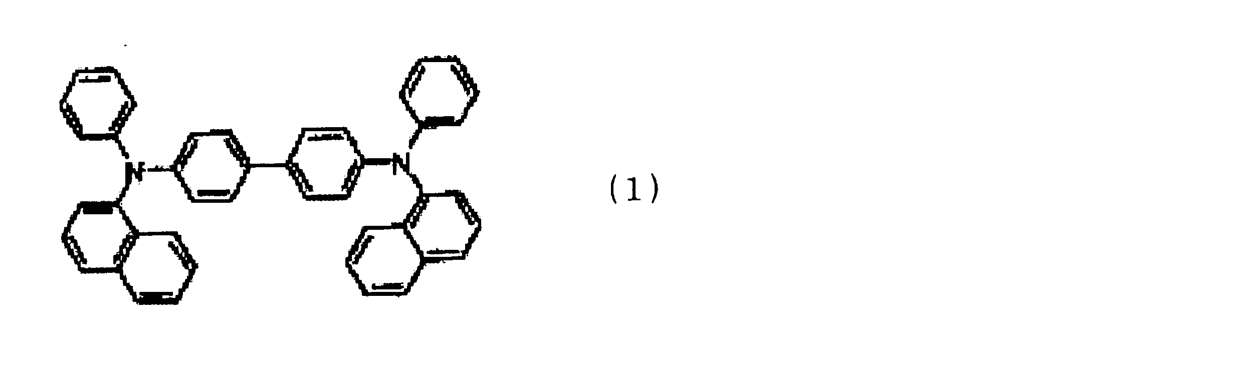
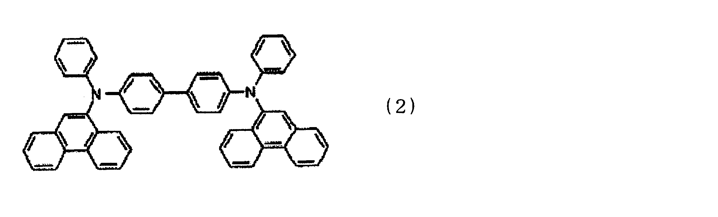
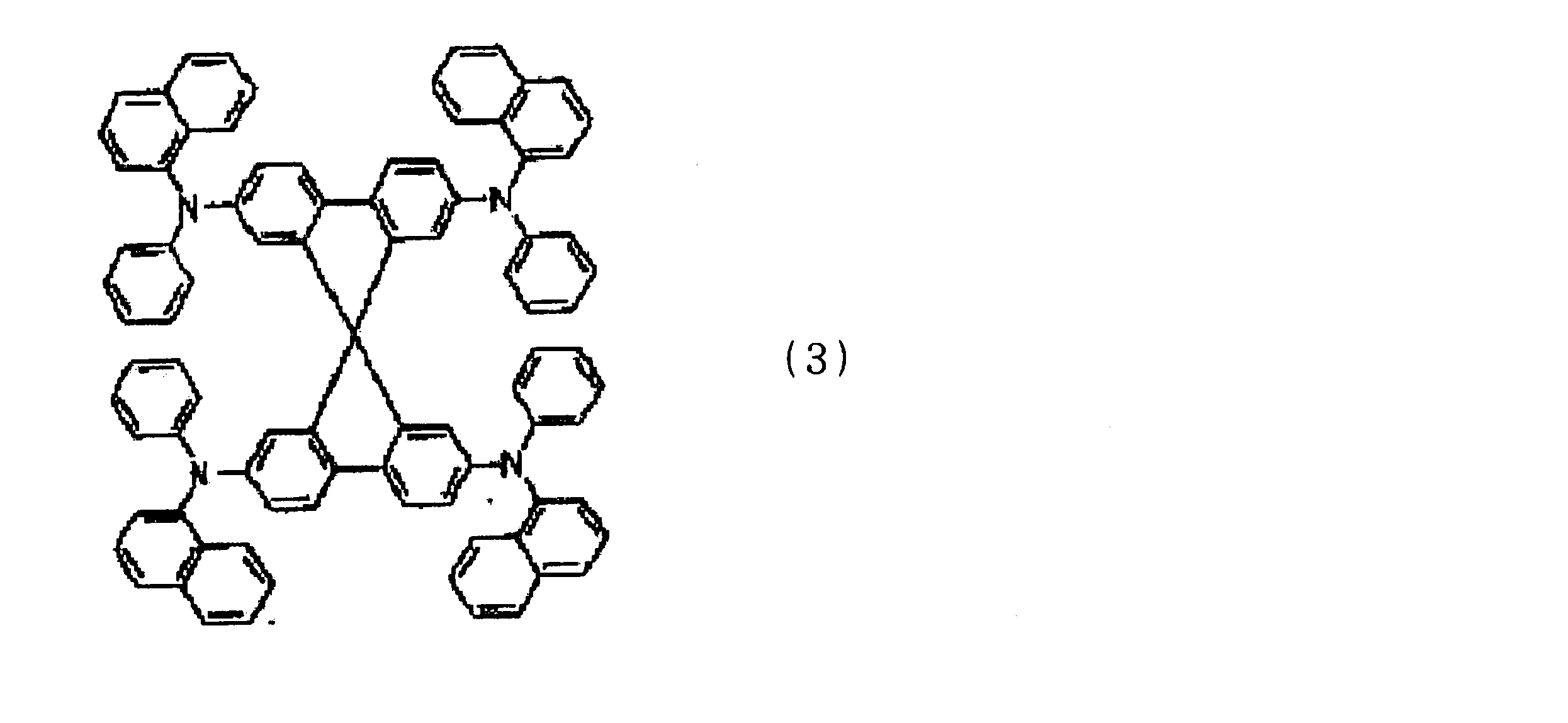
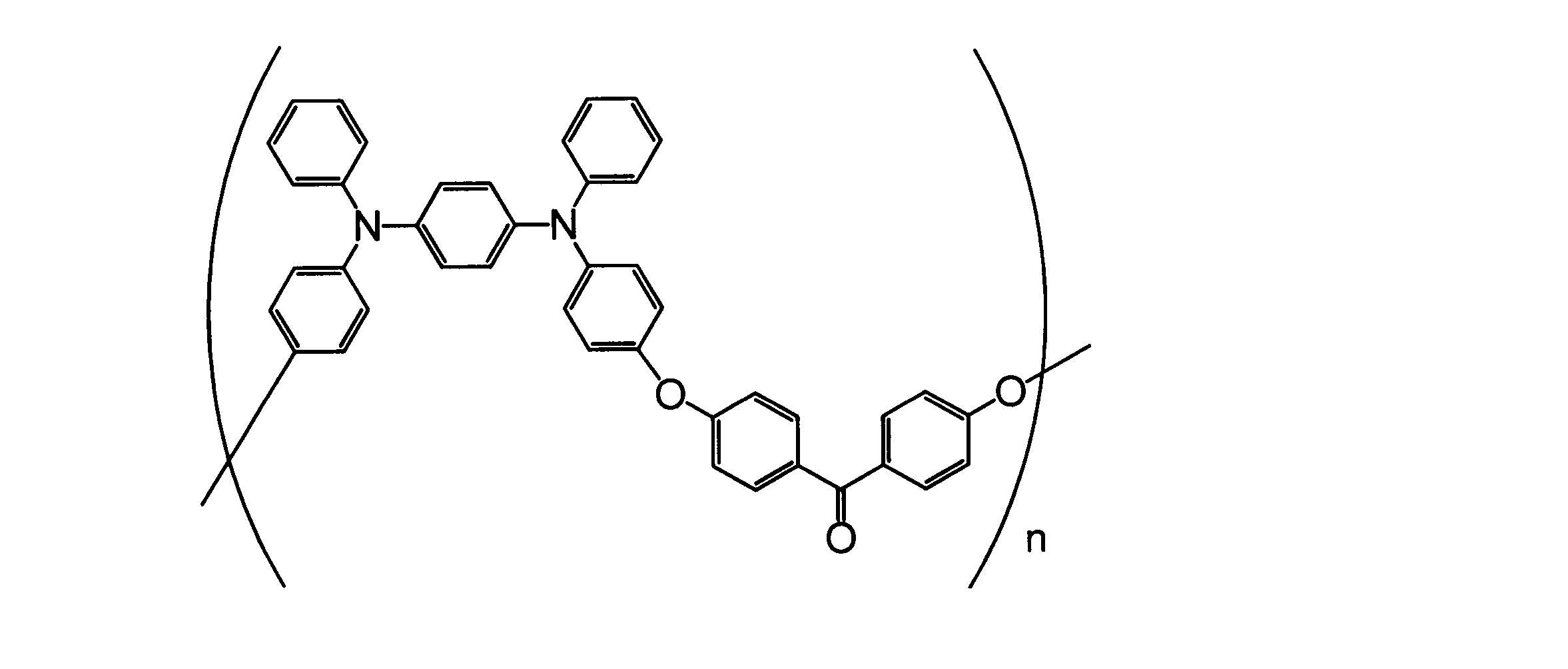
- an aromatic amine compound is preferable, and 4,4′-bis [N- (2-naphthyl) -N-phenyl-amino] biphenyl ( ⁇ -NPD) represented by the following formula (1): ), 4,4′-bis [N- (9-phenanthryl) -N-phenyl-amino] biphenyl (PPD), spiro-NPB represented by the following formula (3), Spiro-TAD represented by (II) and 2-TNATA represented by the following formula (5) are particularly preferred from the viewpoint of the heat resistance of the organic electroluminescence device.
- electron transport materials include oxadiazole derivatives, oxazole derivatives, thiazole derivatives, thiadiazole derivatives, pyrazine derivatives, triazole derivatives, triazine derivatives, perylene derivatives, quinoline derivatives, quinoxaline derivatives, fluorenone derivatives, anthrone derivatives, phenanthroline derivatives, organic Examples thereof include metal complexes, pyridine derivatives, pyrrolopyridine derivatives, pyrimidine derivatives, naphthyridine derivatives, silole derivatives, and the like.
- the charge transport material the above-described hole transport material, electron transport material, and the like can be appropriately selected and used as long as the object of the present invention is not impaired. Of course, other materials can also be used.
- Examples of the luminescent material include 9,10-diarylanthracene derivatives, pyrene, coronene, perylene, rubrene, 1,1,4,4-tetraphenylbutadiene, tris (8-quinolinolato) aluminum complex, tris (4-methyl- 8-quinolinolato) aluminum complex, bis (8-quinolinolato) zinc complex, tris (4-methyl-5-trifluoromethyl-8-quinolinolato) aluminum complex, tris (4-methyl-5-cyano-8-quinolinolato) aluminum Complex, bis (2-methyl-5-trifluoromethyl-8-quinolinolato) [4- (4-cyanophenyl) phenolate] aluminum complex, bis (2-methyl-5-cyano-8-quinolinolato) [4- ( 4-cyanophenyl) phenolate] aluminum , Tris (8-quinolinolato) scandium complex, bis [8- (para-tosyl) aminoquinoline] zinc complex and
- the thickness of the organic functional layer 3 is not uniform depending on the single layer structure or the multilayer structure, but is usually 1000 nm or less, and preferably 50 to 150 nm from the viewpoint of thinning.
- a hole blocking layer, an electron transport layer, and the like may be formed by appropriately selecting a material on the light emitting layer.
- the second electrode 4 is a cathode and plays a role of injecting electrons into the organic functional layer 3.
- the cathode can be made of the same material as that used for the anode, but a metal having a low work function is preferable for efficient electron injection.
- a metal having a low work function is preferable for efficient electron injection.
- tin, magnesium, indium, calcium, A suitable metal such as aluminum or silver or an alloy thereof is used.
- Specific examples include low work function alloy electrodes such as magnesium-silver alloy, magnesium-indium alloy, and aluminum-lithium alloy.
- only 1 type may be used for the material of a cathode, and it may use it combining 2 or more types by arbitrary ratios. Note that the thickness of the cathode is usually the same as that of the anode.
- the back member of the organic EL light emitting device 10 includes a sealing layer 5, a moisture absorption layer 6, and a protective layer 7.
- the sealing layer 5 is formed so as to cover the exposed surface of the organic electroluminescence element on the light-transmitting substrate 1, and the sealing layer 5 according to this embodiment is the main surface of the light-transmitting substrate 1.
- a surface of the anode 2, the organic functional layer 3, and the cathode layer 4 are in direct contact with and covered.
- a protective layer 7 is formed on the sealing layer 5 so as to cover it, and a moisture absorbing layer 6 is formed between the sealing layer 5 and the protective layer 7 so as to be in contact with the protective layer 7. Has been.
- the moisture absorption layer 6 is formed in a hollow rectangular shape while maintaining a constant interval along the outer periphery of the light emitting region so as to surround at least the light emitting region of the light emitting layer constituting the organic functional layer 3. .
- the back member has an end 6 a of the moisture absorbing layer 6 that is longer than the light emitting region end 3 a of the light emitting layer constituting the organic functional layer 3 along the horizontal direction and from the end 5 a of the sealing layer 5. Also short. That is, the end 6 a of the moisture absorbing layer 6 protrudes in the horizontal direction from the light emitting region end 3 a of the light emitting layer of the organic functional layer 3, and the end 5 a of the sealing layer 5 is It protrudes along the horizontal direction from the end 6a.
- the “end portion” refers to a portion that protrudes most outside the organic electroluminescence light emitting device along the horizontal direction
- the “horizontal direction” refers to the main surface of the translucent substrate 1. Parallel direction.
- the “light emitting region of the light emitting layer” refers to a region that emits light in the light emitting layer constituting the organic functional layer 3 when a voltage is applied between the electrodes. This is a region where the functional layer 3 and the second electrode 4 overlap each other, and is a region where light is emitted from the element to the outside.
- the “light emitting region end 3a of the light emitting layer” is the outermost end of the light emitting layer in the region where the first electrode 2, the organic functional layer 3 and the second electrode 4 overlap.
- the distance x in the horizontal direction from the light emitting region end 3a of the light emitting layer to the end 6a of the moisture absorption layer 6 is usually 0.4 mm or more, preferably 1 mm or more, more preferably 10 mm or more.
- the upper limit is usually 100 mm, preferably 50 mm, more preferably 10 mm.
- the position in the horizontal direction is the end of the hygroscopic layer and the position in the vertical direction with respect to the substrate is an arbitrary position, the probability of reaching the hygroscopic layer while moving by a distance x is sealed.
- the film thickness of the sealing layer is usually 200 ⁇ m or less, it is considered that there is a sufficient effect if it is twice or more this thickness. Therefore, x is estimated to be 0.4 mm or more.
- the distance y in the horizontal direction from the end 6a of the hygroscopic layer 6 to the end 5a of the sealing layer 5 is usually 0.1 mm or more, preferably 1 mm or more.
- the upper limit is usually 10 mm, preferably 5 mm.
- the back member of the organic EL light emitting device 10 employs sealing in which the sealing layer 5, the moisture absorbing layer 6 and the protective layer 7 are sequentially laminated, and the end 6a of the moisture absorbing layer 6 is disposed at a predetermined position. Therefore, not only can moisture from the outside be blocked, but also the heat dissipation of the heat generated by the light emitting layer is excellent. Therefore, deterioration of the organic electroluminescence element is suppressed, and stable light emission characteristics can be maintained over a long period of time.
- the protective layer 7 is comprised with the flexible material, the organic electroluminescent light-emitting device 10 can implement
- thermoplastic resin contained in the sealing layer 5 Although it does not specifically limit as a thermoplastic resin contained in the sealing layer 5, for example, a polypropylene, polyethylene, a polystyrene, polyisobutylene, polyester, polyisoprene etc. can be mentioned. These can be used alone or in combination of two or more. Among these, polypropylene, polyethylene, and polyisobutylene are preferable from the viewpoint of low moisture permeability.
- the glass transition temperature of the thermoplastic resin is usually ⁇ 80 ° C. or higher, preferably ⁇ 20 ° C. or higher, from the viewpoint of heat resistance, and the upper limit is not particularly limited.
- the sealing layer 5 may contain components other than the thermoplastic resin, and examples thereof include petroleum resins and cyclic olefin polymers.
- petroleum resins include p. 14 of "14906 Chemical Products” (published by Chemical Industry Daily). 1192, C5 petroleum resin, C9 petroleum resin, C5C9 copolymer petroleum resin, and the like.
- cyclic olefin polymer examples include hydrogenated terpene resins (for example, Clearon P, M, K series), hydrogenated rosin and hydrogenated rosin ester resins (for example, Foral AX, Foral 1105, Pencel A, Ester gum H, superester A series, etc.), disproportionated rosin and disproportionated rosin ester resins (for example, pine crystal series), pentene, isoprene, piperine, 1,3- Hydrogenated dicyclopentadiene resins that are hydrogenated resins of C5 petroleum resins obtained by copolymerizing C5 fractions such as pentadiene (for example, Escholets 5300, 5400 series, Eastotac H series, etc.), thermal decomposition of petroleum naphtha C, such as indene, vinyltoluene, ⁇ or ⁇ -methylstyrene Resin obtained by hydrogenation of C9 petroleum resin obtained by copolymerization of fractions (for example, Alcon
- thermoplastic resin for example, a filler, an ultraviolet absorber, an ultraviolet stabilizer, an antioxidant, a resin stabilizer, and the like may be appropriately added as long as the physical properties of the adhesive are not inhibited.
- the lower limit of the thickness of the sealing layer 5 is usually 1 ⁇ m or more, preferably 10 ⁇ m or more, and the upper limit is usually 200 ⁇ m or less, preferably 150 ⁇ m or less, more preferably 100 ⁇ m or less.
- the moisture absorption layer 6 contains a desiccant
- the desiccant is not particularly limited as long as it is highly hygroscopic.
- alkaline earth metals, alkali metals or oxides thereof, or inorganic porous materials can be used. These can be used alone or in combination of two or more.
- alkaline earth metal or alkali metal oxides and inorganic porous materials are preferable, and calcium oxide and zeolite are particularly preferable.
- the moisture absorption layer 6 may contain components other than the desiccant, and examples thereof include particles and rods made of Si, AlN, and C having high thermal conductivity.
- FIG. 1 is a hollow square, but is not particularly limited as long as it can absorb moisture transmitted from the outside, and depending on the arrangement of the light emitting region of the light emitting layer, a square, a rectangle, a circle, An oval shape or the like can be selected as appropriate.
- a hollow structure or a planar structure may be used as long as moisture from the outside can be blocked.
- the lower limit of the thickness of the moisture absorption layer 6 is usually 0.1 ⁇ m or more, preferably 1 ⁇ m or more, more preferably 10 ⁇ m or more.
- the upper limit is usually 500 ⁇ m or less, preferably 200 ⁇ m or less, more preferably 100 ⁇ m or less.
- the protective layer 7 blocks moisture and oxygen from the outside and also functions as a support when manufacturing the back member. Moreover, the protective layer 7 has flexibility.
- a metal foil or a laminate of a plastic film and an inorganic compound layer can be used.
- the protective layer 7 preferably has a gas barrier property. Examples of the metal having gas barrier properties include aluminum, copper, nickel, alloy materials such as stainless steel and aluminum alloy.
- the laminate of the plastic film and the inorganic compound layer is formed by laminating one layer or multiple layers of an inorganic oxide layer such as silicon oxide or aluminum oxide, or an inorganic nitride layer such as silicon nitride or aluminum nitride on the plastic film. Examples include laminated films.
- metal foil is preferable, and aluminum foil is particularly preferable.
- Use of metal foil is not only preferable from the viewpoint of processing and cost reduction, but also has excellent barrier to moisture and oxygen from the outside, it is easy to bend when necessary, and pinholes when heated or stressed Defects such as cracks are less likely to occur.
- aluminum foil is preferable because it has the best balance between workability and durability.
- the lower limit of the thickness of the protective layer 7 is usually 1 ⁇ m or more, preferably 10 ⁇ m or more.
- the upper limit is usually 500 ⁇ m or less, preferably 200 ⁇ m or less.
- the thickness ⁇ of the protective layer 7 is preferably 0.3 times or more the thickness ⁇ of the sealing layer 5.
- the thickness of the protective layer 7 is 0.3 times or more the thickness of the sealing layer 5
- the heat generated in the organic electroluminescence element is efficiently transmitted to the protective layer 7 via the sealing layer 5, It is considered that heat can be efficiently radiated from the protective layer 7.
- the reason is considered as follows.
- One of the causes of driving deterioration of the organic electroluminescence element is deterioration due to heat generation during driving. In order to suppress the influence of heat generation, it is necessary to efficiently dissipate the heat generated in the organic electroluminescence element.
- the thickness of the organic EL light emitting device 10 is usually 0.1 to 5 mm, preferably 0.5 to 3 mm, more preferably 1 to 2 mm.
- the present invention can be variously modified without departing from the gist thereof.
- the organic electroluminescence element in which the anode 2, the organic functional layer 3, and the cathode 4 are sequentially laminated on the translucent substrate 1 has been described, but the cathode 4,
- An organic electroluminescence element in which the organic functional layer 3 and the anode 2 are sequentially laminated can also be used.
- the moisture absorbing layer 6 having a hollow rectangular shape has been described.
- FIG. 1 the moisture absorbing layer 6 having a hollow rectangular shape has been described.
- a constant interval (for example, an interval x) is provided along the outer periphery of the light emitting region of the light emitting layer. It can also be set as the planar shape which covers all the light emission areas of a light emitting layer, keeping it.
- the configuration of the organic EL light emitting device shown in FIG. 2 is the same as the configuration of the organic EL light emitting device shown in FIG. 1 except for the shape of the moisture absorption layer 6.
- the manufacturing method of the organic EL light emitting device of the present invention includes an element forming step, a back member forming step, and a heat treatment step. Hereinafter, each step will be described.
- An element formation process is a process of forming an organic electroluminescent element, and can employ
- 3 (a) to 3 (c) are schematic cross-sectional views showing the manufacturing process of the organic electroluminescence element of the organic EL light emitting device. A method for manufacturing an organic electroluminescence element will be described with reference to FIGS.
- the translucent substrate 1 is prepared.
- the first electrode 2 is formed on the surface of the translucent substrate 1.
- Formation of the 1st electrode 2 can be normally performed by sputtering method, a vacuum evaporation method, etc.
- the first electrode 2 is formed by using fine metal particles such as silver, fine particles such as copper iodide, carbon black, conductive metal oxide fine particles, conductive polymer fine powder, etc.
- the 1st electrode 2 can also be formed by disperse
- a thin film is directly formed on the light-transmitting substrate 1 by electrolytic polymerization, or the first electrode 2 is formed by applying a conductive polymer on the light-transmitting substrate 1.
- an organic functional layer 3 that forms at least a light emitting layer is formed on the first electrode 2.
- a method for forming the organic functional layer 3 can be appropriately selected depending on the material. For example, a vacuum deposition method, a spin coating method, a dip coating method, a die coating method, a bar coating method, a blade coating method, a roll A coating method, a spray coating method, a capillary coating method, an ink jet method, a screen printing method, a gravure printing method, a flexographic printing method, and the like can be used.
- the second electrode 4 is formed on the organic functional layer 3.
- a method for forming the second electrode 4 a sputtering method, a vacuum evaporation method, or the like can be used.
- FIGS. 4A to 4D are schematic cross-sectional views showing the manufacturing process of the back member of the organic EL light emitting device. With reference to FIGS. 4A to 4D, a method of manufacturing the back member will be described.
- the moisture absorbing layer 6 is formed on the surface of the protective layer 7 so as to surround the light emitting region of the light emitting layer, while maintaining a constant interval along the outer periphery of the light emitting region. Form into shape.
- the method for forming the moisture absorbing layer 6 can be selected as appropriate depending on the material. For example, a dry film forming method such as a vacuum deposition method, insertion of a sheet-like moisture absorbing sheet, spin coating method, dip coating method, etc.
- Wet coating methods such as die coating, bar coating, blade coating, roll coating, spray coating, capillary coating, ink jet, screen printing, gravure printing, flexographic printing, dispenser coating, etc. Can be used.
- a wet film forming method is preferable, and printing methods such as a die coating method, a spray coating method, a screen printing method, a gravure printing method, a flexographic printing method, and a coating method using a dispenser are further included.
- screen printing and dispenser application are particularly preferably employed.
- the protective layer 7 in which the hygroscopic layers 6 are formed in a matrix is maintained at a constant interval along the outer periphery of the hygroscopic layer 6 as shown in FIG. Cut one piece at a time. In addition, you may perform this cutting after the process of forming the next sealing layer.
- the sealing layer 5 including a thermoplastic resin is formed on the moisture absorption layer 6.
- the surface of the hygroscopic layer 6 is entirely covered with the sealing layer 5, and the sealing layer 5 is formed so that the end 5 a of the sealing layer 5 protrudes from the end 6 a of the hygroscopic layer 6.
- a roll coating method, a spin coating method, a screen printing method, a coating method such as spray coating, or a printing method may be used. From the viewpoint of workability, a sheet-like thermoplastic resin is used. A method of applying an adhesive is preferably employed.
- FIGS. 5A to 5D are schematic cross-sectional views showing other manufacturing steps of the back member of the organic EL light emitting device. A method for manufacturing the back member will be described with reference to FIGS.
- a flexible sheet serving as the protective layer 7 as shown in FIG. 5A is prepared.
- the moisture absorption layer 6 is emitted on the surface of the flexible sheet serving as the protective layer 7.
- a flat shape is formed so as to cover the entire light emitting region of the light emitting layer while maintaining a constant interval along the outer periphery of the light emitting region of the layer.
- the formation method of the moisture absorption layer 6 is as having demonstrated in the above.
- the protective layer 7 is cut one by one while maintaining a constant interval along the outer periphery of the moisture absorbing layer 6, and then the moisture absorbing layer 6 is cut as shown in FIG. 5 (d).
- a sealing layer 5 containing a thermoplastic resin is formed thereon.
- FIG. 5D it is good also as a single wafer process which forms the moisture absorption layer 6 in the flexible sheet
- the sealing layer 5 containing a thermoplastic resin is formed on the hygroscopic layer 6.
- the sealing layer 5 is formed in the same manner as in FIG.
- the flexible sheet to be the protective layer 7 is formed by forming a region where the moisture absorption layer 6 is formed into a concave shape in advance, or after forming the moisture absorption layer 6, the protection layer 7 is matched to the shape of the moisture absorption layer 6. Is preferably formed in a concave shape.
- the depth of the recess is preferably substantially equal to the thickness of the hygroscopic layer 6. The reason is that the surface on which the sealing layer 5 is formed coincides with the surface of the hygroscopic layer 6 and the surface of the flexible sheet that becomes the protective layer 7, so that the sealing layer 5 is formed uniformly. For this reason, when the element is sealed with the back member, the adhesiveness between the sealing layer 5 and the element is good, and entry of moisture and oxygen from the outside is prevented.
- the hygroscopic layer 6 is preferably formed in a planar shape that covers the entire light emitting region of the light emitting layer while maintaining a constant interval along the outer periphery of the light emitting region of the light emitting layer, as shown in FIG.
- the reason is that even when a minute defect occurs in the protective layer 7 on the light emitting region for some reason, moisture is blocked by the moisture absorbing layer, thereby preventing deterioration of the element.
- the flexible sheet to be the protective layer 7 is molded into a concave shape in advance in the region where the moisture absorption layer 6 is formed, or after the moisture absorption layer 6 is formed, the protection layer is matched to the shape of the moisture absorption layer 6. In the case where 7 is formed in a concave shape, since the shape to be molded is not complicated, the flexible sheet serving as the protective layer 7 is not subjected to excessive stress, and defects such as pinholes and cracks are less likely to occur.
- FIG. 7A shows a state where the hygroscopic layer 6 is formed on the protective layer 7.
- FIG. 7B the moisture absorption layer 6 is the bottom surface.
- reference numeral 31 denotes a stage, and a surface having a flat surface and rigidity can be used.
- glass, metal such as stainless steel, ceramics, or the like can be used.
- the sealing layer 5 can be formed on a flat surface in which the protective layer 7 and the hygroscopic layer 6 are substantially flush with each other. By forming the sealing layer 5 on a flat surface, it is preferable for the reasons that bubbles do not easily enter and there are no places where the adhesiveness is deteriorated due to deformation.
- the electrode forming surface side of the organic electroluminescent element and the sealing layer forming surface side of the back member are connected to the end of the hygroscopic layer. Are laminated and pasted so that they protrude 0.4 mm or more from the light emitting region end of the light emitting layer along the horizontal direction.
- the heat treatment step is performed by heat-treating the organic electroluminescence element and the back member, which are laminated and bonded, while applying pressure from the organic electroluminescence element side and the back member side under normal pressure, reduced pressure, or high pressure atmosphere. Is called.
- a thermal laminator for the heating, a thermal laminator, an oven, a hot plate, or the like can be used.
- the heating temperature is usually 200 ° C. or lower, preferably 170 ° C. or lower.
- the pressurization can be performed by a pressurizing means such as a laminator, a pressurizing roller or a press, or a high pressure atmosphere. Bonding under reduced pressure is preferable because air bubbles do not enter between the organic electroluminescence element and the back member, so that moisture permeability is reduced and peeling is difficult.
- the heat treatment step includes a treatment (heating press treatment) in which a region of the protective layer 7 outside the light emitting region end portion of the light emitting layer and having no moisture absorbing layer 6 is heated while being heated.
- a treatment heating press treatment
- the thickness of the sealing layer 5 in the region outside the light emitting region end of the light emitting layer is reduced, and moisture and oxygen from the outside that permeate through the layer of the sealing layer 5 are preferably reduced.
- the thickness of the sealing layer 5 in the region where the light emitting region and the hygroscopic layer 6 exist is larger than the thickness of the sealing layer 5 in the region outside the light emitting region end of the light emitting layer and where the hygroscopic layer 6 does not exist.
- FIG. 8 shows an example of sealing an organic electroluminescence element with a back member.
- FIG. 8A shows a first electrode 2, an organic functional layer 3 formed on the first electrode 2, and a second electrode formed on the organic functional layer 3 on the translucent substrate 1. It is a figure of the state which piled up the back member which consists of the protective layer 7, the moisture absorption layer 6, and the sealing layer 5 on the organic electroluminescent element in which the electrode 4 was formed. In this state, the back member is adhered to such an extent that it cannot be peeled off, but may be easily peeled off when used for a long time or in a high temperature and high humidity environment.
- the heat treatment process includes a heat press process shown in FIG.
- Reference numeral 33 in FIG. 8B denotes a heating press member, which is a part of the press device.
- the translucent substrate is disposed on the stage.
- the stage may be heated, the pressurizing member 33 may be heated, or heat press treatment may be performed in a high temperature environment.
- the adhesiveness is excellent, the back member is not peeled off even under long-term use or high temperature and high humidity, and the non-light emitting region is difficult to spread.
- An organic EL light-emitting device with excellent durability can be obtained.
- the heating temperature at the time of hot pressing is usually 50 ° C.
- the organic functional layer 3 is not thermally deteriorated, and the sealing layer 5 can enhance the adhesion with the translucent substrate 1.
- the protective layer 7 and the sealing layer 5 are deformed by the heating press, and the sealing layer 5 becomes thinner than the initial thickness.
- ⁇ is the initial thickness of the sealing layer 5
- ⁇ is the thickness of the sealing layer 5 after hot pressing.
- the moisture that penetrates from the end portion and permeates the sealing layer 5 has a cross-sectional area that increases when it reaches the region where the moisture absorption layer 6 exists and the light emitting region of the sealing layer 5. It is preferable that the concentration is lowered and the organic functional layer 3 is hardly deteriorated.
- the thickness of the organic electroluminescence element on the light emitting region (total of 2, 3, 4) is sufficiently smaller than the thickness of the sealing layer 5, and therefore the sealing layer 5 on the light emitting region.
- the thickness ⁇ of the region where the hygroscopic layer 6 protrudes from the edge of the light emitting region are considered to be substantially the same.
- the deformation amount of the sealing layer 5 by heating press ((1- ⁇ / ⁇ ) ⁇ 100 (%)) is usually 10% or more, preferably 20% or more of the thickness of the sealing layer 5. 90% or less, preferably 80% or less. Within this range, it is preferable that the sealing layer 5 is sufficiently adhered to the light-transmitting substrate 1 to reduce moisture permeability, hardly peel off, and does not break. Further, it is preferable that cracks and pinholes are not easily generated in the protective layer 7.
- the organic EL light-emitting device of the present invention can be manufactured.
- the organic EL light-emitting device of the present invention is, for example, a personal computer, a mobile phone, a digital still camera, a television, a viewfinder type, or a monitor direct view type. It can be applied as a display unit of a video tape recorder, a car navigation device, a pager, an electronic notebook, a calculator, a word processor, a workstation, a video phone, a POS terminal, and a device equipped with a touch panel.
- the organic EL display device of the present invention is a display device using the above-described organic electroluminescence element of the present invention.
- the organic EL display device of the present invention is produced by a method described in “Organic EL display” (Ohm, published on August 20, 2004, written by Shizushi Tokito, Chiba Adachi, and Hideyuki Murata). can do.
- the organic EL illumination of the present invention is illumination using the above-described organic electroluminescence element of the present invention.
- Example 1 The organic EL light emitting device shown in FIG. 1 was manufactured by the following method. First, an organic electroluminescence device having a 2 mm square light emitting region was manufactured by the procedure shown in FIG. ⁇ Formation of hole injection layer on ITO substrate> As an ITO substrate 1, an indium tin oxide (ITO) transparent conductive film (anode 2) having a thickness of 70 nm is formed on a glass substrate 1 having a length of 3.75 cm, a width of 2.5 cm, and a thickness of 0.7 mm. was used.
- ITO indium tin oxide
- a polymer compound having a repeating structure represented by the following formula (6) (PB-1, weight average molecular weight: 52000, number average molecular weight: 32500) and 4-isopropyl-4′-methyldiphenyliodonium tetrakis (pentafluorophenyl) ) Borate was mixed at a mass ratio of 100 to 20, and a composition dissolved in ethyl benzoate was prepared so that the concentration of the mixture was 2.0% by weight.
- This composition was spin-coated on the ITO substrate 1 in the air atmosphere in two stages at a spinner rotation number of 500 rpm for 2 seconds and further at 1500 rpm for 30 seconds. Then, the 30-nm-thick hole injection layer was formed by heating at 230 degreeC for 15 minutes.
- LiF lithium fluoride
- a back member was manufactured according to the procedure shown in FIG. ⁇ Formation of moisture absorption layer>
- An aluminum foil having a thickness of 40 ⁇ m was cut into a 100 mm square.
- Dry Paste-S1 manufactured by SaesGetters
- a screen printer HP-300, manufactured by Neurong Seimitsu Kogyo Co., Ltd.
- a hollow rectangular hygroscopic layer having a thickness of 60 ⁇ m, a width of 3 mm, and a side of 16 mm was formed.
- it moved under a nitrogen atmosphere and baked on a hot plate at 200 ° C. for 30 minutes.
- the aluminum foil was cut into 23 mm square so that the hollow square moisture absorption layer was in the center.
- thermoplastic sheet adhesive made by JTY-0806, 3M sandwiched between two PET films is cut into 23 mm square, and then the PET film on one side is peeled off to cover the entire surface of the moisture absorbing layer. And three thermoplastic sheet adhesives (75 ⁇ m) are stacked and pasted on aluminum foil so that the edge of the sealing layer protrudes 3.5mm from the edge of the hygroscopic layer along the horizontal direction. A layer was formed. In order to make it adhere so that air may not enter between an aluminum foil and a moisture absorption layer, and a sealing layer, the sheet-like adhesive was roller press-bonded on the PET film on a 100 degreeC hotplate.
- the opposite PET film from which the PET film was peeled off is peeled off from the end of the sealing layer, the adhesive surface of the sealing layer covers the light emitting layer of the organic electroluminescence element, and the end of the moisture absorbing layer emits light along the horizontal direction.
- the layer was attached by hand so as to protrude 4 mm from the end of the light emitting region of the layer. Place the glass side of the organic electroluminescence element on a hot plate at 100 ° C., press the aluminum foil of the back member with a roller, and then, outside the light emitting region of the back member, the region where the moisture absorption layer is not formed,
- the organic EL light emitting device shown in FIG. 1 was obtained by applying pressure with a roller. This organic EL light-emitting device is surrounded by a hollow rectangular moisture-absorbing layer while maintaining a constant interval along the outer periphery of the light-emitting region of the light-emitting layer.
- Example 1 (Comparative Example 1) In Example 1, instead of the calcium oxide paste, a water getter sheet (HD-S050914W-40, manufactured by Dynic) having a length of 0.9 cm and a width of 1.4 cm was attached to an aluminum foil, and a thickness of 25 ⁇ m was formed thereon. Four sheets (100 ⁇ m) of thermoplastic sheet-like pressure-sensitive adhesive (manufactured by JTY-0806, 3M) were laminated and pasted. The back member thus obtained and the organic electroluminescence element produced by the same operation as in Example 1 were bonded together by the same operation as in Example 1 to obtain an organic EL light emitting device. In this organic EL light emitting device, the moisture absorbing layer does not surround the light emitting region of the light emitting layer, and the moisture absorbing layer exists only in a part of the upper portion of the light emitting region.
- a water getter sheet (HD-S050914W-40, manufactured by Dynic) having a length of 0.9 cm and a width of 1.4 cm
- Example 1 The organic EL light-emitting devices obtained in Example 1 and Comparative Example 1 were subjected to a storage test in a constant temperature and humidity chamber at 85 ° C. and 85% RH, and shrink growth using an industrial microscope (ECLIPSE LV100D, manufactured by NiKon). The width was measured. The results are shown in Table 1.
- Example 2 The organic EL light emitting device shown in FIG. 2 was manufactured by the following method.
- an organic electroluminescence device having a 7 mm square light emitting region was manufactured by the procedure shown in FIG.
- the manufacturing method of the organic electroluminescence element is the same as that in Example 1.
- a back member was manufactured according to the procedure shown in FIG. ⁇ Formation of moisture absorption layer> An aluminum foil having a thickness of 100 ⁇ m was cut into a 100 mm square. Using Dry Paste-S1 (manufactured by SaesGetters) mainly composed of calcium oxide as a desiccant, on a cut aluminum foil in an air atmosphere, using a screen printer (HP-300, manufactured by Neurong Seimitsu Kogyo Co., Ltd.) A square type moisture absorption layer having a thickness of 50 ⁇ m and a side of 18 mm was formed. Immediately after printing, it moved under a nitrogen atmosphere and baked on a hot plate at 200 ° C. for 30 minutes. The aluminum foil was cut into a square with a side of 22 mm so that the moisture absorption layer was in the center.
- Dry Paste-S1 manufactured by SaesGetters
- a screen printer HP-300, manufactured by Neurong Seimitsu Kogyo Co., Ltd.
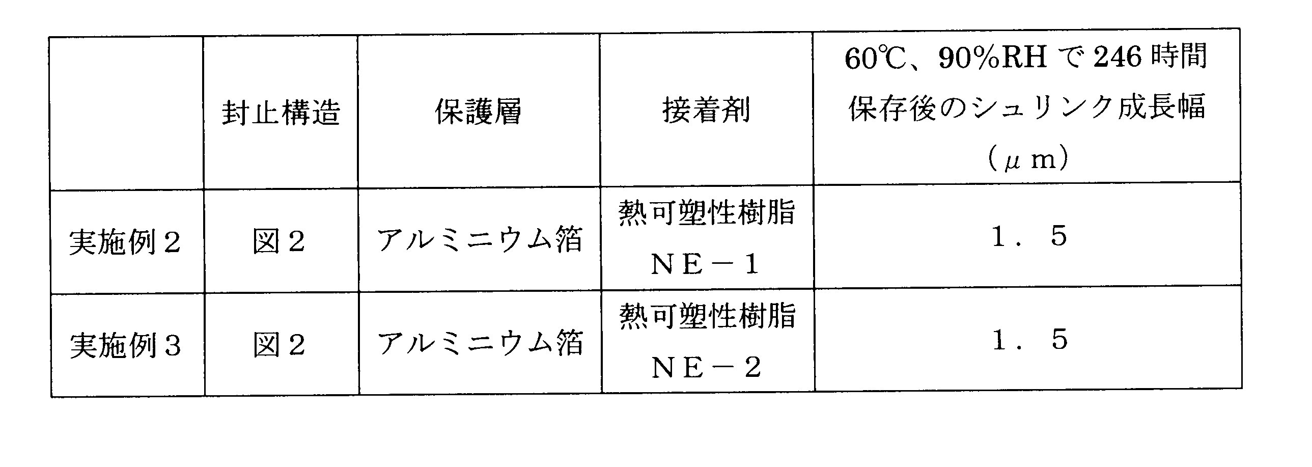
- a sheet-like adhesive having a thickness of 50 ⁇ m is sandwiched between two PET films and a thermoplastic resin NE-1 in which polyisobutylene and a cyclopentadiene / dicyclopentadiene copolymer are mixed at a mass ratio of 28:72. Cut to. Thereafter, the thermoplastic resin NE-1 is removed so that the PET film on one side is peeled to cover the entire surface of the hygroscopic layer and the end of the sealing layer protrudes 2 mm from the end of the hygroscopic layer along the horizontal direction.
- Two coated sheet-like pressure-sensitive adhesives (100 ⁇ m) were stacked and attached to an aluminum foil to form a sealing layer. In order to make it adhere so that air may not enter between an aluminum foil and a moisture absorption layer, and a sealing layer, the sheet-like adhesive was roller press-bonded on the PET film on a 100 degreeC hotplate.
- the PET film of the sealing layer is peeled off, the adhesive surface of the sealing layer covers the light emitting layer of the organic electroluminescence element, and the end of the hygroscopic layer protrudes 1 mm from the end of the light emitting region of the light emitting layer along the horizontal direction. Pasted by hand. Place the glass side of the organic electroluminescence element on a hot plate at 100 ° C., press the aluminum foil of the back member with a roller, and then, outside the light emitting region of the back member, the region where the moisture absorption layer is not formed, The organic EL light emitting device shown in FIG. 2 was obtained by applying pressure with a roller. The entire surface of the organic EL light emitting device is covered with a square moisture absorbing layer that is 1 mm larger than the outer periphery of the light emitting region of the light emitting layer.
- Example 3 In Example 2, a mass ratio of polyisobutylene, cyclopentadiene / dicyclopentadiene copolymer and polybutene was used instead of the 50 ⁇ m-thick sheet-like adhesive in which the thermoplastic resin NE-1 was sandwiched between two PET films.
- FIG. 2 shows the same procedure as in Example 2 except that a 50 ⁇ m thick sheet-like adhesive in which the thermoplastic resin NE-2 mixed at a ratio of 23:58:19 was sandwiched between two PET films was used. The organic EL light emitting device shown was obtained.
- Test Example 2 The organic EL light emitting devices obtained in Examples 2 to 3 were subjected to a storage test in a constant temperature and humidity chamber of 60 ° C. and 90% RH, and the shrink growth width was measured using an industrial microscope (ECLIPSE LV100D, manufactured by Nikon). Measured. The results are shown in Table 2.
- Example 3 The organic EL light-emitting device obtained in Example 2 was subjected to a storage test in a thermostatic chamber at 85 ° C., and the shrinkage growth width was measured using an industrial microscope (ECLIPSE LV100D, manufactured by Nikon). After storage for 560 hours The shrink growth width was 10 ⁇ m or less.
- Example 4 The organic EL light-emitting device obtained in Example 2 was subjected to a storage test in a constant temperature bath of ⁇ 20 ° C., and the shrinkage growth width was measured using an industrial microscope (ECLIPSE LV100D, manufactured by Nikon). As a result, it was stored for 250 hours. Later, the shrink growth width was 5 ⁇ m or less.
- Example 4 An organic electroluminescence device having the structure shown in FIG. 1 was prepared by the following method.
- the ITO substrate 1 is formed by forming an indium tin oxide (ITO) transparent conductive film with a thickness of 70 nm as an anode 2 on a glass substrate 1 having a length of 3.75 cm, a width of 2.5 cm, and a thickness of 0.7 mm.
- ITO indium tin oxide
- the polymer compound PB-1 having the following repeating structure represented by the following formula and 4-isopropyl-4′-methyldiphenyliodonium tetrakis (pentafluorophenyl) borate were mixed at a weight ratio of 100: 20.
- a composition dissolved in ethyl benzoate so as to have a concentration of 2.0% by weight was prepared.
- This composition was spin-coated on the ITO substrate 1 in the air atmosphere in two stages of spinner rotation speed of 500 rpm for 2 seconds and 1500 rpm for 30 seconds. Then, the 30-nm-thick hole injection layer was formed by heating at 230 degreeC for 15 minutes.
- lithium fluoride (LiF) is deposited on the light emitting layer by a vacuum deposition method to a film thickness of 0.5 nm to form an electron injection layer, and then aluminum is deposited by a vacuum deposition method to a film thickness of 80 nm.
- the cathode 4 was formed.
- a back member was manufactured according to the procedure shown in FIG. ⁇ Formation of back member> A 40 ⁇ m thick aluminum foil was cut into 22 mm squares to form a protective layer. Next, a desiccant (Moist Catch CCA Co., Ltd., 80 um thick) was cut into 18 mm square in N 2 and thermocompression bonded at 120 ° C. to the center of the aluminum foil to form a moisture absorption layer. At this time, 2 mm around the hygroscopic layer is only aluminum foil.
- a sealing layer a 40 ⁇ m sheet in which polyisobutylene and cyclopentadiene / dicyclopentadiene copolymer are mixed at a mass ratio of 1: 1 is cut into 22 mm square, and thermocompression-bonded to the surface where the moisture absorption layer is exposed. Bonding was made into a back member. This back member is formed only on the protective layer and the sealing layer in the periphery 2 mm of the region where the moisture absorption layer is formed.
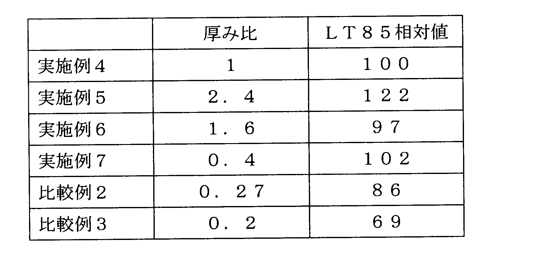
- Examples 5 to 7, Comparative Examples 2 and 3 A back member was formed in the same manner as in Example 4 except that the thickness of the aluminum foil and the thickness of the pressure-sensitive adhesive were changed as follows.
- the sealing layer of the back member covers the light emitting layer of the organic electroluminescence element, and the moisture absorption layer protrudes along the outer periphery while keeping a distance of 1 mm from the edge of the light emitting layer in the horizontal direction with the substrate. And bonded by thermocompression bonding at 110 ° C. Thereafter, a frame-shaped polycarbonate heating press member is disposed over the entire area of 2 mm width around the hygroscopic layer where the aluminum foil and the translucent substrate are bonded by the sealing layer.
- Test Example 5 The organic EL light-emitting devices obtained in Examples 4 to 7 and Comparative Examples 2 and 3 were subjected to a drive test at 65.3 mA / cm 2 . The time until the luminance reduction rate (L / L0) reached 0.85 (LT85) was compared.
- Table 1 shows an example in which the ratio of the protective layer thickness to the sealing layer thickness (thickness of the protective layer / sealing layer thickness) as the thickness ratio and the LT85 time of Comparative Example 1 is set to 100 as the relative value of LT85. The relative value of LT85 is described.
- Example 6 The organic EL light emitting devices obtained in Example 8-12 and Comparative Example 4-7 were subjected to a storage test for 315 hours in a constant temperature and humidity chamber at 85 ° C. and 85% RH. The device was caused to emit light and the shrink width was measured in the same manner as in Example 1.
- Example 13 An organic EL light emitting device was produced in the same manner as in Example 5.
- the thickness of the sealing layer in the hot-pressed region after the hot pressing was 14 ⁇ m, and the pressing amount of the protective layer was 26 ⁇ m.
- Example 8 An organic EL light emitting device was fabricated in the same manner as in Example 5 except that the back member and the organic electroluminescent element were bonded by thermocompression bonding at 110 ° C., and then the heat pressing at 110 ° C. and 10 MPa was not performed. . Since the heating press was not performed, the protective layer pressing amount was 0 ⁇ m.
- Test Example 7 The organic EL light-emitting devices obtained in Example 13 and Comparative Example 8 were subjected to a storage test in a constant temperature and humidity chamber at 85 ° C. and 85% RH for 287 hours, and the shrink width was measured as in Test Example 2.
Abstract
Description
したがって、本発明の課題は、外部からの水分の透過と拡散を防止し、安定な発光特性を長期間維持することが可能な有機EL発光装置を提供することにある。また、本発明の課題は、このような有機EL発光装置を、より簡便な工程で効率良く製造できる有機EL発光装置の製造方法を提供することにある。
<1>透光性基板と、該透光性基板上に形成された第1の電極と、該第1の電極上に形成され、少なくとも発光層を有する有機機能層と、該有機機能層上に形成された第2の電極と、少なくとも前記第1の電極、前記第2の電極及び前記有機機能層の表面を覆うように形成された熱可塑性樹脂を含む封止層と、該封止層上に形成され、可撓性を有する保護層と、該保護層と前記封止層との間に設けられ、前記発光層の発光領域を少なくとも囲うように形成された乾燥剤を含む吸湿層とを備え、該吸湿層の端部は、水平方向に沿って前記発光領域の端部よりも0.4mm以上長く突出し、かつ前記封止層の端部よりも短い、有機エレクトロルミネッセンス発光装置。
<2>前記発光領域上の前記保護層の厚みが、前記発光領域上の前記封止層の厚みの0.3倍以上である、前記<1>に記載の有機エレクトロルミネッセンス発光装置。
<3>前記吸湿層が形成されていない領域の前記封止層の厚みの方が、前記発光領域の前記封止層の厚みよりも薄い、前記<1>または<2>に記載の有機エレクトロルミネッセンス発光装置。
<4>前記吸湿層の端部から前記封止層の端部までの水平方向における間隔が0.1mm以上である、前記<1>~<3>のいずれか1に記載の有機エレクトロルミネッセンス発光装置。
<5>前記吸湿層がアルカリ土類金属、アルカリ金属及びそれらの酸化物、並びに無機多孔質材料から選ばれる少なくとも1種を含む、前記<1>~<4>のいずれか1に記載の有機エレクトロルミネッセンス発光装置。
<6>前記吸湿層の厚みが0.1μm以上、500μm以下である、前記<1>~<5>のいずれか1に記載の有機エレクトロルミネッセンス発光装置。
<7>前記封止層の厚みが1μm以上、200μm以下である、前記<1>~<6>のいずれか1に記載の有機エレクトロルミネッセンス発光装置。
<8>前記封止層の厚みが10μm以上、100μm以下である、前記<1>~<6>のいずれか1に記載の有機エレクトロルミネッセンス発光装置。
<9>前記保護層の厚みが10μm以上、200μm以下である、前記<1>~<6>のいずれか1に記載の有機エレクトロルミネッセンス発光装置。
<10>第1の電極が形成された透光性基板の該第1の電極上に、少なくとも発光層を有する有機機能層を形成し、次いで該有機機能層上に第2の電極を形成して有機エレクトロルミネッセンス素子を得る素子形成工程と、保護層としての可撓性シート上に乾燥剤を含む吸湿層を形成する工程と、該保護層の厚みの3.3倍以下の厚みであって、熱可塑性樹脂を含む封止層を、該吸湿層上に形成して背面部材を得る背面部材形成工程と、前記有機エレクトロルミネッセンス素子の前記第2の電極形成面側と、前記背面部材の封止層形成面側とを、前記吸湿層が前記発光層の発光領域を少なくとも囲い、かつ前記吸湿層の端部が水平方向に沿って前記発光層の発光領域端部よりも0.4mm以上突出するように重ね合わせて加熱処理する熱処理工程と、をこの順に含む有機エレクトロルミネッセンス発光装置の製造方法。
<11>第1の電極が形成された透光性基板の該第1の電極上に、少なくとも発光層を有する有機機能層を形成し、次いで該有機機能層上に第2の電極を形成して有機エレクトロルミネッセンス素子を得る素子形成工程と、保護層としての可撓性シート上に乾燥剤を含む吸湿層を形成する工程と、該保護層の厚みの3.3倍以下の厚みであって、熱可塑性樹脂を含む封止層を、該吸湿層上に形成して背面部材を得る背面部材形成工程と、前記有機エレクトロルミネッセンス素子の前記第2の電極形成面側と、前記背面部材の封止層形成面側とを、前記吸湿層が前記発光層の発光領域を少なくとも囲い、かつ前記吸湿層の端部が水平方向に沿って前記発光層の発光領域端部よりも0.4mm以上突出するように重ね合わせて加熱処理する熱処理工程と、をこの順に含む製造方法によって製造された有機エレクトロルミネッセンス発光装置。
<12>前記<11>に記載の有機エレクロルミネッセンス発光装置を用いた、有機エレクロルミネッセンス表示装置。
<13>前記<11>に記載の有機エレクロルミネッセンス発光装置を用いた、有機エレクロルミネッセンス照明装置。
<14>前記<11>に記載の有機エレクロルミネッセンス発光装置を用いた、有機エレクロルミネッセンス電気装置。
更に、本発明によれば、このような有機EL発光装置をより簡便な工程で効率良く製造することができる。
なお、“重量%”と“質量%”とは同義である。
図1に示す有機EL発光装置10は、有機エレクトロルミネッセンス素子と、その背面に形成された背面部材とから構成されるものである。以下、有機エレクトロルミネッセンス素子及び背面部材について詳細に説明する。
有機EL発光装置10の有機エレクトロルミネッセンス素子は、透光性基板1と、透光性基板1上に形成された第1の電極2と、第1の電極2上に形成された有機機能層3と、有機機能層3上に形成された第2の電極4を有するものである。有機エレクトロルミネッセンス素子の有機機能層3の発光層で発光された光は、透光性基板1を通して取り出されるものである。
有機エレクトロルミネッセンス素子の構成及びその構成材料は、従来公知のものを採用することができるが、構成材料として、例えば、次のものを挙げることができる。
透光性基板1は有機エレクトロルミネッセンス素子の支持体となるものであり、石英やガラスの板、金属板や金属箔、プラスチックフィルムやシート等を用いることができる。特にガラス板や、ポリエステル、ポリメタクリレート、ポリカーボネート、ポリスルホン等の透明な合成樹脂の板が好ましい。
合成樹脂製基板を使用する場合には、ガスバリア性に留意する必要がある。透光性基板1のガスバリア性が小さすぎると、透光性基板1を透過した外気により有機エレクトロルミネッセンス素子が劣化することがある。このため、合成樹脂製基板の少なくとも片面に緻密なシリコン酸化膜等を設けてガスバリア性を確保する方法も好ましい方法の一つである。
透光性基板1の厚みは、通常0.01~10mm、好ましくは0.1~1mmである。
第1の電極2は陽極であり、有機機能層3へ正孔注入の役割を果たすものである。この陽極は、通常、アルミニウム、金、銀、ニッケル、パラジウム、白金等の金属、インジウム及び/又はスズの酸化物等の金属酸化物、ヨウ化銅などのハロゲン化金属、カーボンブラックの他、ポリ(3-メチルチオフェン)、ポリピロール、ポリアニリン等の導電性高分子等により構成される。
有機機能層3は、少なくとも発光層を有するものであれば、単層構造でも、多層構造でもよい。多層構造の例としては、正孔注入輸送層、発光層及び電子注入層からなる3層構造や、正孔注入層、正孔輸送層、発光層、正孔阻止層及び電子注入層からなる5層構造などが挙げられ、適宜選択することが可能である。


第2の電極4は陰極であり、有機機能層3に電子を注入する役割を果たすものである。この陰極は、陽極に使用される材料と同様のものを用いることが可能であるが、効率良く電子注入を行なうには、仕事関数の低い金属が好ましく、例えば、スズ、マグネシウム、インジウム、カルシウム、アルミニウム、銀等の適当な金属又はそれらの合金が用いられる。具体例としては、マグネシウム-銀合金、マグネシウム-インジウム合金、アルミニウム-リチウム合金等の低仕事関数合金電極を挙げることができる。また、陰極の材料は、1種のみを用いてもよく、2種以上を任意の比率で組み合わせて用いてもよい。
なお、陰極の厚みは、通常、陽極と同様である。
一方、有機EL発光装置10の背面部材は、封止層5と、吸湿層6と、保護層7を具備するものである。封止層5は、有機エレクトロルミネッセンス素子の透光性基板1上の露出面を覆うように形成されるものであり、本実施形態に係る封止層5は、透光性基板1の主面の一部と、陽極2、有機機能層3及び陰極層4の表面に直接接触して被覆する状態で形成されている。また、封止層5上には、これを覆うように保護層7が形成されており、封止層5と保護層7の間には、保護層7に接触するように吸湿層6が形成されている。本実施形態に係る吸湿層6は、有機機能層3を構成する発光層の発光領域を少なくとも取り囲むように、発光領域の外周に沿って一定の間隔を保ちながら中空方形の形状に形成されている。
ここで、本明細書において「端部」とは、水平方向に沿って有機エレクトロルミネッセンス発光装置の外側に最も突出した部分をいい、「水平方向」とは透光性基板1の主面に対して平行な方向をいう。また、本明細書において「発光層の発光領域」とは、電極間に電圧を印加したときに有機機能層3を構成する発光層の中で発光する領域をいい、第1の電極2、有機機能層3及び第2の電極4が重なり合った領域であって、素子から発光が外部に出射される領域である。「発光層の発光領域端部3a」とは、第1の電極2、有機機能層3及び第2の電極4が重なり合った領域における発光層の最外端部とする。
xが0.4mm以上であることによって、背面部材端部から侵入してくる水分を効率よく吸湿層で吸湿し、発光層の劣化を抑制することができる。
本発明者らは、背面部材端部から侵入してきた封止層中の水分子を効率よく吸湿層に到達するための部材構成を考察した結果、封止層中の水分子の位置が、基板に対して水平方向の位置が吸湿層端部であり、基板に対して垂直方向の位置が任意の位置である場合、そこから距離xだけ移動する間に吸湿層に到達する確率は、封止層の膜厚がxと同等か薄い方が大きいという結論に達した。後述の通り、封止層の膜厚は通常200μm以下なので、この厚みの2倍以上あれば十分効果があると考えられる。従って、xは0.4mm以上であると推察される。
また、有機EL発光装置10は、保護層7が可撓性材料で構成されているため、従来に比して軽量化、薄膜化が可能になるとともに、低コスト化を実現することができる。更に、封止層5が熱可塑性樹脂を含むため、有機エレクトロルミネッセンス素子が劣化した場合に当該封止層の熱可塑性樹脂を溶融させて基板をリサイクルすることもできる。
封止層5に含まれる熱可塑性樹脂としては特に限定されないが、例えばポリプロピレン、ポリエチレン、ポリスチレン、ポリイソブチレン、ポリエステル、ポリイソプレンなどを挙げることができる。これらは単独で又は2種以上組み合わせて使用することができる。中でも、低透湿性の観点から、ポリプロピレン、ポリエチレン、ポリイソブチレンが好ましい。また、熱可塑性樹脂のガラス転移温度は、耐熱性の観点から、通常-80℃以上、好ましくは-20℃以上であり、上限は特に限定されない。
石油樹脂としては、例えば「14906の化学商品」(化学工業日報社刊行)のp.1192に記載のC5系石油樹脂、C9系石油樹脂、C5C9共重合石油樹脂等が挙げられる。
環状オレフィン系重合体は、具体的には、水添テルペン系樹脂(例えば、クリアロンP,M,Kシリーズ)、水添ロジン及び水添ロジンエステル系樹脂(例えば、Foral AX,Foral1105,ペンセルA,エステルガムH,スーパーエステルAシリーズ等)、不均化ロジン及び不均化ロジンエステル系樹脂(例えば、パインクリスタルシリーズ等)、石油ナフサの熱分解で生成するペンテン、イソプレン、ピペリン、1,3-ペンタジエン等のC5留分を共重合して得られるC5系石油樹脂の水添加樹脂である水添ジシクロペンタジエン系樹脂(例えば、エスコレッツ5300,5400シリーズ、Eastotac Hシリーズ等)、石油ナフサの熱分解で生成するインデン、ビニルトルエン、α又はβ-メチルスチレンなどのC9留分を共重合して得られるC9系石油樹脂を水添した樹脂(例えば、アルコンP又はMシリーズ)、上記したC5留分とC9留分の共重合石油樹脂を水添した樹脂(例えば、アイマーブシリーズ)等を挙げることができる。
吸湿層6には乾燥剤が含まれるが、乾燥剤としては吸湿性の高いものであれば特に限定されるものではない。例えば、アルカリ土類金属、アルカリ金属若しくはそれらの酸化物、又は無機多孔質材料などを挙げることができる。これらは単独で又は2種以上を組み合わせて使用することができる。中でも、吸湿性と取り扱いの安全性の観点から、アルカリ土類金属又はアルカリ金属の酸化物、無機多孔質材料が好ましく、酸化カルシウム、ゼオライトが特に好ましい。
吸湿層6は、乾燥剤以外の成分を含有していてもよく、例えば、高熱伝導性のSi,AlN,Cからなる粒子、ロッドなどを挙げることができる。
吸湿層6の厚みは、その下限値は、通常0.1μm以上、好ましくは1μm以上、より好ましくは10μm以上である。またその上限値は、通常500μm以下、好ましくは200μm以下、より好ましくは100μm以下である。
保護層7は、外部からの水分や酸素を遮断するとともに、背面部材を製造する際の支持体としても機能するものである。また、保護層7は、可撓性を有する。
保護層7は、通常、金属箔又はプラスチックフィルムと無機化合物層の積層体などを用いることができる。保護層7は、ガスバリア性を有するものが好ましい。ガスバリア性を有する金属としては、例えば、アルミニウム、銅、ニッケルや、ステンレス、アルミニウム合金などの合金材料などが挙げられる。また、プラスチックフィルムと無機化合物層の積層体としては、プラスチックフィルムに酸化ケイ素、酸化アルミニウムなどの無機酸化物の層、窒化ケイ素、窒化アルミニウム等の無機窒化物の層を一層又は多層積層してなる積層フィルムなどがあげられる。中でも、好ましくは金属箔であり、特に好ましくはアルミニウム箔である。金属箔を用いると加工やコスト低減の観点から好ましいだけでなく、外部からの水分や酸素の遮断性に優れ、必要に応じて屈曲加工しやすく、加熱したり応力がかかった際にピンホールやクラックなどの欠陥が生じにくい。特にアルミニウム箔は、加工性と耐久性を最もバランスよく兼ね備えており好ましい。
保護層7の厚みは、その下限値は、通常1μm以上、好ましくは10μm以上である。またその上限値は、通常500μm以下、好ましくは200μm以下である。
この理由は次のように考えられる。有機エレクトロルミネッセンス素子の駆動劣化の原因の一つに、駆動時の発熱による劣化が上げられる。発熱の影響を抑えるためには、有機エレクトロルミネッセンス素子で発生した熱を効率よく放熱する必要がある。放熱するためには、背面部材の最外層である保護層7に効率よく熱を伝え、保護層7で熱を受け取りやすくすることが考えられる。有機エレクトロルミネッセンス素子からの熱を効率よく移動させるためには、封止層5の「単位面積当たりの熱抵抗」を下げる必要がある。保護層7で熱を受け取りやすくするためには、保護層7の「単位面積当たりの熱容量」を大きくする必要がある。封止層5の「単位面積当たりの熱抵抗」は封止層5の厚みに比例し、保護層7の「単位面積当たりの熱容量」は保護層7の厚みに比例する。封止層5の「単位面積当たりの熱抵抗」は小さいほど熱伝導性が高く、保護層7の「単位面積当たりの熱容量」は大きいほど熱をためやすいため、有機エレクトロルミネッセンス素子で発生した熱を効率よく保護層7へ移動して保護層7に熱を溜めやすく、有機エレクトロルミネッセンス素子の温度上昇を抑制し、駆動時の素子劣化を抑制する、と考えられる。
発明者らは後述の実施例に示すように、鋭意検討の結果、保護層7の厚みが封止層5の厚みの0.3倍以上である場合に駆動寿命が長い素子を得ることができることを見出した。
本発明の有機EL発光装置の製造方法は、素子形成工程と、背面部材形成工程と、熱処理工程を含むものである。以下、各工程について説明する。
素子形成工程は有機エレクトロルミネッセンス素子を形成する工程であり、公知の方法を採用することが可能であるが、例えば、次の方法により行うことができる。図3(a)~(c)は、有機EL発光装置の有機エレクトロルミネッセンス素子の製造工程を示す概略断面図である。図3(a)~(c)を参照しながら、有機エレクトロルミネッセンス素子の製造方法について説明する。
第1の電極2の形成は、通常、スパッタリング法、真空蒸着法等により行うことができる。また、銀等の金属微粒子、ヨウ化銅等の微粒子、カーボンブラック、導電性の金属酸化物微粒子、導電性高分子微粉末等を用いて第1の電極2を形成する場合には、適当なバインダー樹脂溶液に分散させて、透光性基板1上に塗布することにより第1の電極2を形成することもできる。さらに、導電性高分子の場合は、電解重合により直接透光性基板1上に薄膜を形成したり、透光性基板1上に導電性高分子を塗布して第1の電極2を形成することもできる(Appl.Phys.Lett.,60巻,2711頁,1992年)。
有機機能層3の形成方法としては、材料に応じて適宜選択することが可能であるが、例えば、真空蒸着法、スピンコート法、ディップコート法、ダイコート法、バーコート法、ブレードコート法、ロールコート法、スプレーコート法、キャピラリーコート法、インクジェット法、スクリーン印刷法、グラビア印刷法、フレキソ印刷法などを用いることができる。
第2の電極4の形成方法としては、スパッタリング法、真空蒸着法などを用いることができる。
図4(a)~(d)は、有機EL発光装置の背面部材の製造工程を示す概略断面図である。図4(a)~(d)を参照しながら、背面部材の製造方法について説明する。
次に、図4(b)に示すように、保護層7の表面に吸湿層6を、発光層の発光領域を取り囲むように、発光領域の外周に沿って一定の間隔を保ちながら中空方形の形状に形成する。
吸湿層6の形成方法としては、材料に応じて適宜選択することが可能であるが、例えば、真空蒸着法などの乾式成膜法、シート状の吸湿シートの挿入、スピンコート法、ディップコート法、ダイコート法、バーコート法、ブレードコート法、ロールコート法、スプレーコート法、キャピラリーコート法、インクジェット法、スクリーン印刷法、グラビア印刷法、フレキソ印刷法、ディスペンサによる塗布法などの湿式成膜法などを用いることができる。中でも、印刷パターンの自由度とコスト低減の観点から、湿式成膜法が好ましく、ダイコート法、スプレーコート法、スクリーン印刷法、グラビア印刷法、フレキソ印刷法、ディスペンサによる塗布法などの印刷法が更に好ましく、スクリーン印刷、ディスペンサ塗布が特に好ましく採用される。
封止層5の形成方法としては、ロールコート、スピンコート、スクリーン印刷法、スプレーコートなどのコーティング法、印刷法等の方法を用いてもよいが、作業性の観点から、シート状の熱可塑性粘着剤を貼付する方法が好ましく採用される。
次に、上記工程により得られた有機エレクトロルミネッセンス素子と、背面部材とを用いて、有機エレクトロルミネッセンス素子の電極形成面側と、背面部材の封止層形成面側とを、吸湿層の端部が水平方向に沿って発光層の発光領域端部よりも0.4mm以上突出するように重ね合わせて貼合する。
熱処理工程は、重ね合わせて貼合した有機エレクトロルミネッセンス素子と背面部材とを、常圧、減圧、あるいは高圧雰囲気下で、有機エレクトロルミネッセンス素子側と背面部材側から加圧しながら加熱処理することによって行われる。加熱は熱ラミネータやオーブン、ホットプレートなどを用いることができる。加熱温度は、通常、200℃以下、好ましくは170℃以下である。加圧は、ラミネーター、加圧ローラやプレス機などの加圧手段、あるいは高圧雰囲気等によって加圧することができる。減圧下での貼合は、有機エレクトロルミネッセンス素子と背面部材との間に気泡が入らないため、水分の透過性を低減し、かつ剥がれにくくなり好ましい。
熱処理工程は、発光層の発光領域端部より外側であって吸湿層6が存在しない保護層7の領域を加熱しながら加圧する処理(加熱プレス処理)を含むことが、特に好ましい。この処理を有することにより、発光層の発光領域端部より外側の領域の封止層5の厚みが薄くなり、封止層5の層内を透過する外部からの水分や酸素が低減され好ましい。また、発光領域および吸湿層6が存在する領域の封止層5の厚みの方が、発光層の発光領域端部より外側であって吸湿層6が存在しない領域の封止層5の厚みより厚いため、外部から封止層5を透過してきた水分や酸素が発光領域および吸湿層6が存在する領域の封止層5内で拡散され、水分や酸素が発光層に到達して発光層を劣化させる確率を低減することができ好ましい。
加熱プレス時の加熱温度は、通常50℃以上、好ましくは60℃以上、通常200℃以下、好ましくは170℃以下である。この温度範囲で加熱プレスすることにより、有機機能層3が熱劣化せず、かつ、封止層5が透光性基板1との密着性を高めることができる。
また、加熱プレスにより、保護層7および封止層5が変形し、封止層5は当初厚みよりも薄くなる。図8(c)において、βは封止層5の当初厚みであり、γは加熱プレス後の封止層5の厚みである。β>γであることから、端部から侵入して封止層5を透過する水分は、封止層5の吸湿層6が存在する領域および発光領域上に到達すると断面積が大きくなるため水分濃度が低下し、有機機能層3を劣化させにくく好ましい。なお、図8(c)において、発光領域上の有機エレクトロルミネッセンス素子の厚み(2、3、4の合計)は封止層5の厚みに比べて十分薄いため、発光領域上の封止層5の厚みと、発光領域端部から吸湿層6が突出している領域の厚みβとはほぼ同じ厚みと見なされる。
また、封止層5の加熱プレスによる変形量((1-γ/β)×100(%))は、通常、封止層5の厚みの10%以上、好ましくは20%以上であり、通常90%以下、好ましくは80%以下である。この範囲であると、封止層5が十分透光性基板1に密着して水分の透過性を低減し、かつ剥がれにくくなり、また、破断することなく、好ましい。また、保護層7に亀裂やピンホールが発生しにくく好ましい。
本発明の有機EL表示装置は、上述の本発明の有機エレクトロルミネッセンス素子を用いた表示装置である。本発明の有機EL表示装置の型式や構造については特に制限はなく、本発明の有機エレクトロルミネッセンス素子を用いて常法に従って組み立てることができる。例えば、「有機ELディスプレイ」(オーム社、2004年8月20日発行、時任静士、安達千波矢、村田英幸著)に記載されているような方法で、本発明の有機EL表示装置を作製することができる。
本発明の有機EL照明は、上述の本発明の有機エレクトロルミネッセンス素子を用いた照明である。本発明の有機EL照明の型式や構造については特に制限はなく、本発明の有機エレクトロルミネッセンス素子を用いて常法に従って作製することができる。
図1に示す有機EL発光装置を以下の方法により製造した。
先ず、図3に示す手順にて2mm角の発光領域を持つ有機エレクトロルミネッセンス素子を製造した。
<ITO基板への正孔注入層の形成>
ITO基板1として、縦3.75cm、横2.5cm、厚み0.7mmのガラス基板1上に、膜厚70nmのインジウム・スズ酸化物(ITO)透明導電膜(陽極2)が形成されたものを用いた。
次いで、下記式(6)に示す繰り返し構造を有する高分子化合物(PB-1、重量平均分子量:52000、数平均分子量:32500)と、4-イソプロピル-4’-メチルジフェニルヨードニウムテトラキス(ペンタフルオロフェニル)ボラートとを質量比100対20で混合し、混合物の濃度が2.0重量%となるように安息香酸エチルに溶解させた組成物を調製した。この組成物を、大気雰囲気中で、前記ITO基板1上に、スピナ回転数500rpmで2秒、更に1500rpmで30秒の2段階でスピンコートした。その後、230℃で15分間加熱することで、膜厚30nmの正孔注入層を形成した。

次いで、正孔輸送層として、上記式(2)に示す4,4’-ビス[N-(9-フェナントリル)-N-フェニル-アミノ]ビフェニル(PPD)を膜厚40nmとなるように真空蒸着法により製膜した。
次いで、発光層としてトリス(8-ヒドロキシキノリナート)アルミニウム(Alq3)を膜厚60nmとなるように真空蒸着法により製膜した。
次いで、発光層上にフッ化リチウム(LiF)を膜厚0.5nmとなるように真空蒸着法によって蒸着し電子注入層を形成した。正孔注入層から電子注入層までを有機機能層3とした。
次いで、アルミニウムを膜厚80nmとなるように真空蒸着法によって蒸着し、陰極4を形成した。
<吸湿層の形成>
厚さ40μmのアルミニウム箔を100mm角に裁断した。乾燥剤として酸化カルシウムを主剤としたDryPaste-S1(SaesGetters製)を用い、裁断したアルミニウム箔上に、大気雰囲気中で、スクリーン印刷機(HP-300、ニューロング精密工業(株)製)により、厚さ60μm、幅3mm、一辺16mmの中空方形の吸湿層を形成した。印刷後、直ちに窒素雰囲気下に移動し、ホットプレート上で200℃30分ベークした。中空方形の吸湿層が中央になるようにアルミニウム箔を23mm角に裁断した。
2枚のPETフィルムに挟みこまれた厚さ25μmの熱可塑性シート状粘着剤(JTY-0806、3M製)を23mm角に裁断後、片側のPETフィルムを剥離し、吸湿層の全面を被覆し、かつ封止層の端部が水平方向に沿って吸湿層の端部から3.5mm突出するように、熱可塑性シート状粘着剤3枚(75μm)を重ねてアルミニウム箔に貼り付け、封止層を形成した。アルミニウム箔及び吸湿層と、封止層との間に空気が入らないように密着させるために、100℃のホットプレート上で、シート状粘着剤をPETフィルムの上からローラ圧着した。
封止層の先にPETフィルムを剥離した反対側のPETフィルムを剥離し、封止層の粘着面が有機エレクトロルミネッセンス素子の発光層を覆い、かつ吸湿層の端部が水平方向に沿って発光層の発光領域端部から4mm突出するように手で貼り付けた。有機エレクトロルミネッセンス素子のガラス側を100℃のホットプレートに載せ、背面部材のアルミニウム箔をローラで圧着し、次いで、背面部材の発光領域より外側であって吸湿層が形成されていない領域を、さらにローラで加圧し、図1に示す有機EL発光装置を得た。この有機EL発光装置は、発光層の発光領域の外周に沿って一定の間隔を保ちながら中空方形の吸湿層で囲まれている。
実施例1において、酸化カルシウムのペーストの代わりに縦0.9cm、横1.4cmの水分ゲッターシート(HD-S050914W-40、ダイニック社製)をアルミニウム箔に貼り付け、その上に厚さ25μmの熱可塑性シート状粘着剤(JTY-0806、3M製)を4枚(100μm)重ねて貼り付けた。このようにして得られた背面部材と、実施例1と同様の操作により作製した有機エレクトロルミネッセンス素子とを、実施例1と同様の操作により貼り合わせて、有機EL発光装置を得た。なお、この有機EL発光装置は、吸湿層が発光層の発光領域を囲っておらず、吸湿層は発光領域の上部の一部のみに存在している。
実施例1及び比較例1で得られた有機EL発光装置について、85℃、85%RHの恒温恒湿槽で保存試験を行い、工業用顕微鏡(ECLIPSE LV100D,NiKon製)を用いてシュリンクの成長幅を計測した。その結果を表1に示す。

図2に示す有機EL発光装置を以下の方法により製造した。
<吸湿層の形成>
厚さ100μmのアルミニウム箔を100mm角に裁断した。乾燥剤として酸化カルシウムを主剤としたDryPaste-S1(SaesGetters製)を用い、裁断したアルミニウム箔上に、大気雰囲気中で、スクリーン印刷機(HP-300、ニューロング精密工業(株)製)により、厚さ50μm、一辺18mmの正方形型の吸湿層を形成した。印刷後、直ちに窒素雰囲気下に移動し、ホットプレート上で200℃30分ベークした。吸湿層が中央になるように一辺22mmの正方形にアルミニウム箔を裁断した。
ポリイソブチレンとシクロペンタジエン・ジシクロペンタジエン共重合体を質量比28:72の割合で混合した熱可塑性樹脂NE-1が2枚のPETフィルムで挟まれた厚さ50μmのシート状粘着剤を22mm角に裁断した。その後、片側のPETフィルムを剥離し、吸湿層の全面を被覆し、かつ封止層の端部が水平方向に沿って吸湿層の端部から2mm突出するように、熱可塑性樹脂NE-1を被覆したシート状粘着剤2枚(100μm)を重ねてアルミニウム箔に貼り付け、封止層を形成した。アルミニウム箔及び吸湿層と、封止層との間に空気が入らないように密着させるために、100℃のホットプレート上で、シート状粘着剤をPETフィルムの上からローラ圧着した。
封止層のPETフィルムを剥離し、封止層の粘着面が有機エレクトロルミネッセンス素子の発光層を覆い、かつ吸湿層の端部が水平方向に沿って発光層の発光領域端部から1mm突出するように手で貼り付けた。有機エレクトロルミネッセンス素子のガラス側を100℃のホットプレートに載せ、背面部材のアルミニウム箔をローラで圧着し、次いで、背面部材の発光領域より外側であって吸湿層が形成されていない領域を、さらにローラで加圧し、図2に示す有機EL発光装置を得た。この有機EL発光装置は、発光層の発光領域の外周より1mm大きい正方形の吸湿層によって全面が覆われている。
実施例2において、熱可塑性樹脂NE-1が2枚のPETフィルムで挟まれた厚さ50μmのシート状粘着剤の代わりに、ポリイソブチレンとシクロペンタジエン・ジシクロペンタジエン共重合体とポリブテンを質量比23:58:19の割合で混合した熱可塑性樹脂NE-2が2枚のPETフィルムで挟まれた厚さ50μmのシート状粘着剤を用いた以外は、実施例2と同様にして図2に示す有機EL発光装置を得た。
実施例2~3で得られた有機EL発光装置について、60℃、90%RHの恒温恒湿槽で保存試験を行い、工業用顕微鏡(ECLIPSE LV100D,Nikon製)を用いてシュリンクの成長幅を計測した。その結果を表2に示す。
実施例2で得られた有機EL発光装置について、85℃の恒温槽で保存試験を行い、工業用顕微鏡(ECLIPSE LV100D,Nikon製)を用いてシュリンクの成長幅を計測した結果、560時間保存後、シュリンク成長幅は10μm以下であった。
実施例2で得られた有機EL発光装置について、-20℃の恒温槽で保存試験を行い、工業用顕微鏡(ECLIPSE LV100D,Nikon製)を用いてシュリンクの成長幅を計測した結果、250時間保存後、シュリンク成長幅は5μm以下であった。
図1に示す構造を有する有機エレクトロルミネッセンス素子を以下の方法で作成した。
ITO基板1には、縦3.75cm、横2.5cm、厚み0.7mmのガラス基板1上に、膜厚70nmのインジウム・スズ酸化物(ITO)透明導電膜が陽極2として形成されたものを用いた。
次いで、以下に示す繰り返し構造を有する下記式に表す高分子化合物PB-1と4-イソプロピル-4’-メチルジフェニルヨードニウムテトラキス(ペンタフルオロフェニル)ボラートとを重量比100対20で混合し、混合物の濃度が2.0重量%となるように安息香酸エチルに溶解させた組成物を調製した。この組成物を、大気雰囲気中で、前記ITO基板1上に、スピナ回転数500rpmで2秒、そして1500rpmで30秒の2段階でスピンコートした。その後、230℃で15分間加熱することで、膜厚30nmの正孔注入層を形成した。
次いで、正孔輸送層として下記式に表す4,4’-ビス[N-(9-フェナントリル)-N-フェニル-アミノ]ビフェニル(PPD)を膜厚40nm真空蒸着法により製膜した。

次いで、発光層としてトリス(8-ヒドロキシキノリナート)アルミニウム(Alq3)を膜厚60nm真空蒸着法により製膜した。正孔注入層から発光層までを有機機能層3とした。
次いで、発光層上にフッ化リチウム(LiF)を膜厚0.5nmとなるように真空蒸着法によって蒸着し電子注入層を形成した後に、アルミニウムを膜厚80nmとなるように真空蒸着法によって蒸着し、陰極4を形成した。
<背面部材の形成>
厚さ40μmのアルミ箔を22mm角に裁断し、保護層とした。次いで、N2中で、乾燥剤(モイストキャッチCCA共同印刷(株)製厚さ80um)を18mm角に切断し、アルミ箔の中央に120℃で熱圧着し、吸湿層とした。このとき、吸湿層の周囲2mmはアルミ箔のみである。次に乾燥剤を下向きにしてアルミ箔を平らな台に置き、吸湿層の形状にあわせて吸湿層が形成されていない領域をローラーで加圧して保護層を成型し、保護層と吸湿層を略同一面とした。次いで、封止層として、ポリイソブチレンとシクロペンタジエン・ジシクロペンタジエン共重合体とを質量比1:1で混合した40μmのシートを22mm角に裁断し、吸湿層が露出した面に熱圧着して貼り合わせ、背面部材とした。この背面部材は、吸湿層が形成されている領域の周囲2mmは、保護層上と封止層のみで形成されている。
アルミ箔の厚みと粘着剤の厚みを以下のように変更した以外は実施例4と同様に背面部材を形成した。

このようにして得られた背面部材の封止層が有機エレクトロルミネッセンス素子の発光層を覆い、吸湿層が基板と水平方向に発光層端部より1mmの間隔を保ちながら外周に沿って突出するように配置し、110℃で熱圧着して貼り合わせた。その後、アルミ箔と透光性基板が封止層によって接着されている、吸湿層の周囲2mm幅の領域全体に、枠状のポリカーボネート製の加熱プレス部材を配置し、油圧プレス機にて、110℃、10MPaにて加熱プレスし、有機EL発光装置を作製した。(図3および図8(c) x=1.0、y=2.0)
実施例4~7及び比較例2、3で得られた有機EL発光装置について、65.3mA/cm2で駆動試験を行った。輝度低下率(L/L0)が0.85になるまでの時間(LT85)を比較した。表1に、厚み比として保護層厚みと封止層厚みの比(保護層厚み/封止層厚み)と、LT85の相対値として、比較例1のLT85の時間を100とした場合の実施例のLT85の相対値を記す。
吸湿層と発光領域端部との距離が、基板と水平方向に0.5~3mmの間隔を保ちながら外周に沿って突出するようにした以外は、実施例5と同様にして、有機EL発光装置を作製した。(図3および図8(c) x=0.5~3.0、y=2.0)
吸湿層と発光領域端部との距離が、基板と水平方向に-0.5~0.3mmの間隔を保ちながら外周に沿って突出するようにした以外は、実施例5と同様にして、有機EL発光装置を作製した。(図3および図8(c) x=-0.5~0.3、y=2.0)
実施例8-12及び比較例4-7で得られた有機EL発光装置について、85℃85%RHの恒温恒湿槽で315時間保存試験を行った。この素子を発光させて実施例1と同様にシュリンク幅を計測した。

実施例5と同様にして、有機EL発光装置を作製した。加熱プレス後の加熱プレスした領域の封止層厚みは14μmであり、保護層押下げ量は26μmであった。
背面部材と有機エレクトロルミネッセンス素子を110℃で熱圧着して貼り合わせた後、110℃、10MPaでの加熱プレスを行わなかった以外は、実施例5と同様にして、有機EL発光装置を作製した。加熱プレスを行っていないので、保護層押下げ量は0μmであった。
実施例13及び比較例8で得られた有機EL発光装置について、85℃85%RHの恒温恒湿槽で287時間保存試験を行い、試験例2と同様にシュリンク幅を計測した。

試験例6より、発光領域からの基板と水平方向の吸湿層突出幅は0.5μm以上でシュリンク幅が小さく良好となることが分かる。
試験例7より、加熱プレスによって、保護層が押下げられ、封止層が薄くなっていると、シュリンク幅が小さく良好であることが分かる。
本出願は2011年8月5日出願の日本特許出願(特願2011-172178)に基づくものであり、その内容はここに参照として取り込まれる。
2 第1の電極
2a 第2の電極の取り出し電極
3 有機機能層
3a 有機機能層3を構成する発光層の発光領域端部
4 第2の電極
5 封止層
5a 封止層5の端部
6 吸湿層
6a 吸湿層6の端部
7 保護層
10 有機EL発光装置
15 接着剤
16 乾燥剤
17 封止缶
20 有機EL発光装置
30 有機EL発光装置
31 ステージ
32 ローラ
33 加熱プレス部材
x 発光層の発光領域端部3aから吸湿層6の端部6aまでの水平方向における間隔
y 吸湿層6の端部6aから封止層5の端部5aまでの水平方向における間隔
α 保護層7の厚み
β 封止層5の当初厚み
γ 加熱プレス処理後の封止層5の厚み
Claims (14)
- 透光性基板と、
該透光性基板上に形成された第1の電極と、
該第1の電極上に形成され、少なくとも発光層を有する有機機能層と、
該有機機能層上に形成された第2の電極と、
少なくとも前記第1の電極、前記第2の電極及び前記有機機能層の表面を覆うように形成された熱可塑性樹脂を含む封止層と、
該封止層上に形成され、可撓性を有する保護層と、
該保護層と前記封止層との間に設けられ、前記発光層の発光領域を少なくとも囲うように形成された乾燥剤を含む吸湿層とを備え、
該吸湿層の端部は、水平方向に沿って前記発光領域の端部よりも0.4mm以上長く突出し、かつ前記封止層の端部よりも短い、有機エレクトロルミネッセンス発光装置。 - 前記発光領域上の前記保護層の厚みが、前記発光領域上の前記封止層の厚みの0.3倍以上である、請求項1に記載の有機エレクトロルミネッセンス発光装置。
- 前記吸湿層が形成されていない領域の前記封止層の厚みの方が、前記発光領域の前記封止層の厚みよりも薄い、請求項1または2に記載の有機エレクトロルミネッセンス発光装置。
- 前記吸湿層の端部から前記封止層の端部までの水平方向における間隔が0.1mm以上である、請求項1~3のいずれか1項に記載の有機エレクトロルミネッセンス発光装置。
- 前記吸湿層がアルカリ土類金属、アルカリ金属及びそれらの酸化物、並びに無機多孔質材料から選ばれる少なくとも1種を含む、請求項1~4のいずれか1項に記載の有機エレクトロルミネッセンス発光装置。
- 前記吸湿層の厚みが0.1μm以上、500μm以下である、請求項1~5のいずれか1項に記載の有機エレクトロルミネッセンス発光装置。
- 前記封止層の厚みが1μm以上、200μm以下である、請求項1~6のいずれか1項に記載の有機エレクトロルミネッセンス発光装置。
- 前記封止層の厚みが10μm以上、100μm以下である、請求項1~6のいずれか1項に記載の有機エレクトロルミネッセンス発光装置。
- 前記保護層の厚みが10μm以上、200μm以下である、請求項1~6のいずれか1項に記載の有機エレクトロルミネッセンス発光装置。
- 第1の電極が形成された透光性基板の該第1の電極上に、
少なくとも発光層を有する有機機能層を形成し、
次いで該有機機能層上に第2の電極を形成して有機エレクトロルミネッセンス素子を得る素子形成工程と、
保護層としての可撓性シート上に乾燥剤を含む吸湿層を形成する工程と、
該保護層の厚みの3.3倍以下の厚みであって、熱可塑性樹脂を含む封止層を、該吸湿層上に形成して背面部材を得る背面部材形成工程と、
前記有機エレクトロルミネッセンス素子の前記第2の電極形成面側と、前記背面部材の封止層形成面側とを、前記吸湿層が前記発光層の発光領域を少なくとも囲い、かつ前記吸湿層の端部が水平方向に沿って前記発光層の発光領域端部よりも0.4mm以上突出するように重ね合わせて加熱処理する熱処理工程と、
をこの順に含む有機エレクトロルミネッセンス発光装置の製造方法。 - 第1の電極が形成された透光性基板の該第1の電極上に、
少なくとも発光層を有する有機機能層を形成し、
次いで該有機機能層上に第2の電極を形成して有機エレクトロルミネッセンス素子を得る素子形成工程と、
保護層としての可撓性シート上に乾燥剤を含む吸湿層を形成する工程と、
該保護層の厚みの3.3倍以下の厚みであって、熱可塑性樹脂を含む封止層を、該吸湿層上に形成して背面部材を得る背面部材形成工程と、
前記有機エレクトロルミネッセンス素子の前記第2の電極形成面側と、前記背面部材の封止層形成面側とを、前記吸湿層が前記発光層の発光領域を少なくとも囲い、かつ前記吸湿層の端部が水平方向に沿って前記発光層の発光領域端部よりも0.4mm以上突出するように重ね合わせて加熱処理する熱処理工程と、
をこの順に含む製造方法によって製造された有機エレクトロルミネッセンス発光装置。 - 請求項11に記載の有機エレクロルミネッセンス発光装置を用いた、有機エレクロルミネッセンス表示装置。
- 請求項11に記載の有機エレクロルミネッセンス発光装置を用いた、有機エレクロルミネッセンス照明装置。
- 請求項11に記載の有機エレクロルミネッセンス発光装置を用いた、有機エレクロルミネッセンス電気装置。
Priority Applications (6)
| Application Number | Priority Date | Filing Date | Title |
|---|---|---|---|
| KR1020187034225A KR102157996B1 (ko) | 2011-08-05 | 2012-08-02 | 유기 일렉트로 루미네선스 발광 장치 및 그 제조 방법 |
| CN201280037760.9A CN103718646B (zh) | 2011-08-05 | 2012-08-02 | 有机电致发光装置及其制造方法 |
| KR1020147002656A KR20140048225A (ko) | 2011-08-05 | 2012-08-02 | 유기 일렉트로 루미네선스 발광 장치 및 그 제조 방법 |
| EP12822555.4A EP2741577B1 (en) | 2011-08-05 | 2012-08-02 | Organic electroluminescent light emitting device and method for manufacturing same |
| JP2013527997A JP6070558B2 (ja) | 2011-08-05 | 2012-08-02 | 有機エレクトロルミネッセンス発光装置及びその製造方法 |
| US14/173,002 US9385334B2 (en) | 2011-08-05 | 2014-02-05 | Organic electroluminescence light-emitting device and production method thereof |
Applications Claiming Priority (2)
| Application Number | Priority Date | Filing Date | Title |
|---|---|---|---|
| JP2011-172178 | 2011-08-05 | ||
| JP2011172178 | 2011-08-05 |
Related Child Applications (1)
| Application Number | Title | Priority Date | Filing Date |
|---|---|---|---|
| US14/173,002 Continuation US9385334B2 (en) | 2011-08-05 | 2014-02-05 | Organic electroluminescence light-emitting device and production method thereof |
Publications (1)
| Publication Number | Publication Date |
|---|---|
| WO2013021924A1 true WO2013021924A1 (ja) | 2013-02-14 |
Family
ID=47668432
Family Applications (1)
| Application Number | Title | Priority Date | Filing Date |
|---|---|---|---|
| PCT/JP2012/069762 WO2013021924A1 (ja) | 2011-08-05 | 2012-08-02 | 有機エレクトロルミネッセンス発光装置及びその製造方法 |
Country Status (7)
| Country | Link |
|---|---|
| US (1) | US9385334B2 (ja) |
| EP (1) | EP2741577B1 (ja) |
| JP (1) | JP6070558B2 (ja) |
| KR (2) | KR20140048225A (ja) |
| CN (1) | CN103718646B (ja) |
| TW (1) | TWI603514B (ja) |
| WO (1) | WO2013021924A1 (ja) |
Cited By (7)
| Publication number | Priority date | Publication date | Assignee | Title |
|---|---|---|---|---|
| JP2014164888A (ja) * | 2013-02-22 | 2014-09-08 | Mitsubishi Chemicals Corp | 有機電界発光装置及びその製造方法 |
| JP2015108045A (ja) * | 2013-12-03 | 2015-06-11 | 古河電気工業株式会社 | 樹脂組成物、有機電子デバイス素子封止用樹脂シート、有機エレクトロルミネッセンス素子および画像表示用装置 |
| KR20150078504A (ko) * | 2013-12-30 | 2015-07-08 | 엘지디스플레이 주식회사 | 유기발광 표시장치 |
| WO2018163937A1 (ja) * | 2017-03-09 | 2018-09-13 | パイオニア株式会社 | 発光装置 |
| JP2019514175A (ja) * | 2016-04-12 | 2019-05-30 | エルジー・ケム・リミテッド | 封止フィルム |
| JP2020021558A (ja) * | 2018-07-30 | 2020-02-06 | 双葉電子工業株式会社 | 有機el素子及びその製造方法 |
| WO2020066496A1 (ja) * | 2018-09-27 | 2020-04-02 | 富士フイルム株式会社 | 電子デバイス積層体の製造方法、および、電子デバイス積層体 |
Families Citing this family (10)
| Publication number | Priority date | Publication date | Assignee | Title |
|---|---|---|---|---|
| US11038144B2 (en) * | 2010-12-16 | 2021-06-15 | Samsung Display Co., Ltd. | Organic light-emitting display apparatus |
| KR20150011231A (ko) * | 2013-07-22 | 2015-01-30 | 삼성디스플레이 주식회사 | 유기 발광 표시 장치 및 이의 제조 방법 |
| JP6367920B2 (ja) * | 2014-03-12 | 2018-08-01 | パナソニック株式会社 | 有機el装置の設計方法及び有機el装置の製造方法 |
| KR102557315B1 (ko) | 2015-05-08 | 2023-07-19 | 삼성디스플레이 주식회사 | 유기 발광 표시 장치 |
| KR102550693B1 (ko) | 2016-08-04 | 2023-07-04 | 삼성디스플레이 주식회사 | 플렉시블 디스플레이 장치 및 제조 방법 |
| CN107425134B (zh) * | 2017-05-03 | 2019-09-24 | 京东方科技集团股份有限公司 | 一种有机电致发光显示面板、其制作方法及显示装置 |
| WO2018230525A1 (ja) * | 2017-06-14 | 2018-12-20 | パナソニックIpマネジメント株式会社 | 表示装置および表示装置の製造方法 |
| KR102482255B1 (ko) | 2018-10-26 | 2022-12-28 | 현대모비스 주식회사 | 파워팩의 커버장치 |
| CN111599934A (zh) * | 2020-05-07 | 2020-08-28 | Tcl华星光电技术有限公司 | 显示面板及其制备方法 |
| CN115536835A (zh) * | 2022-10-25 | 2022-12-30 | 吉林大学 | 一种基于三苯胺及其衍生物的聚芳醚类聚合物及其制备方法和应用 |
Citations (8)
| Publication number | Priority date | Publication date | Assignee | Title |
|---|---|---|---|---|
| JP2002175877A (ja) * | 2000-09-27 | 2002-06-21 | Seiko Epson Corp | 有機エレクトロルミネッセンス装置、有機エレクトロルミネッセンス装置の製造方法、電子機器 |
| JP2003168555A (ja) * | 2001-11-29 | 2003-06-13 | Sumitomo Electric Ind Ltd | エレクトロルミネッセンス表示装置 |
| JP2003323975A (ja) * | 2002-04-30 | 2003-11-14 | Seiko Epson Corp | 電気光学装置及び電子機器 |
| JP2006080094A (ja) | 2005-11-30 | 2006-03-23 | Seiko Epson Corp | 有機エレクトロルミネッセンス装置及びその製造方法並びに電子機器 |
| JP2007123102A (ja) * | 2005-10-28 | 2007-05-17 | Kyocera Corp | 有機elディスプレイ |
| JP2010055861A (ja) | 2008-08-27 | 2010-03-11 | Panasonic Corp | 発光装置及び発光装置の製造方法 |
| JP2010080289A (ja) * | 2008-09-26 | 2010-04-08 | Dainippon Printing Co Ltd | 有機エレクトロルミネッセンスパネル、及びその製造方法 |
| JP2011009076A (ja) * | 2009-06-25 | 2011-01-13 | Panasonic Electric Works Co Ltd | 有機エレクトロルミネッセンス素子 |
Family Cites Families (23)
| Publication number | Priority date | Publication date | Assignee | Title |
|---|---|---|---|---|
| JP2001307871A (ja) | 2000-04-21 | 2001-11-02 | Toppan Printing Co Ltd | エレクトロルミネッセンス素子 |
| JP3936151B2 (ja) * | 2000-05-08 | 2007-06-27 | 双葉電子工業株式会社 | 有機el素子 |
| JP4926324B2 (ja) | 2001-02-08 | 2012-05-09 | 三星モバイルディスプレイ株式會社 | 有機elデバイス |
| JP3975739B2 (ja) | 2001-12-14 | 2007-09-12 | 旭硝子株式会社 | 有機elディスプレイ用対向基板の製造方法および有機elディスプレイの製造方法 |
| CN1678639A (zh) * | 2002-07-24 | 2005-10-05 | 粘合剂研究公司 | 可转换的压敏粘合剂胶带及其在显示屏上的用途 |
| JP4178887B2 (ja) | 2002-09-04 | 2008-11-12 | 凸版印刷株式会社 | 有機エレクトロルミネッセンス素子 |
| JP2004171806A (ja) | 2002-11-18 | 2004-06-17 | Toppan Printing Co Ltd | 有機エレクトロルミネッセンス素子 |
| JP4325249B2 (ja) | 2003-03-31 | 2009-09-02 | 凸版印刷株式会社 | 有機エレクトロルミネッセンス素子の製造方法 |
| JP4325248B2 (ja) | 2003-03-31 | 2009-09-02 | 凸版印刷株式会社 | 有機エレクトロルミネッセンス素子の製造方法 |
| US6998648B2 (en) * | 2003-08-25 | 2006-02-14 | Universal Display Corporation | Protected organic electronic device structures incorporating pressure sensitive adhesive and desiccant |
| JP2005320404A (ja) * | 2004-05-07 | 2005-11-17 | Nagase Chemtex Corp | 電子部品シール用接着剤組成物及び有機電界発光装置の製造方法 |
| EP1804310B1 (en) | 2005-12-30 | 2016-10-19 | Samsung Display Co., Ltd. | Organic light emiting device and method of manufacturing the same |
| US20070172971A1 (en) | 2006-01-20 | 2007-07-26 | Eastman Kodak Company | Desiccant sealing arrangement for OLED devices |
| JP5362948B2 (ja) | 2006-06-27 | 2013-12-11 | パナソニック株式会社 | 有機エレクトロルミネッセンス発光装置及び有機エレクトロルミネッセンス照明装置 |
| JP5144041B2 (ja) | 2006-07-26 | 2013-02-13 | パナソニック株式会社 | 有機エレクトロルミネッセンス発光装置及び有機エレクトロルミネッセンス照明装置 |
| JP4861206B2 (ja) | 2007-01-26 | 2012-01-25 | パナソニック電工株式会社 | 有機エレクトロルミネッセンス発光装置及び有機エレクトロルミネッセンス照明装置 |
| JP2008210788A (ja) | 2007-02-02 | 2008-09-11 | Toppan Printing Co Ltd | 有機el素子 |
| KR101383713B1 (ko) * | 2007-03-21 | 2014-04-09 | 삼성디스플레이 주식회사 | 표시 장치 및 그 제조 방법 |
| JP2009117181A (ja) * | 2007-11-06 | 2009-05-28 | Hitachi Displays Ltd | 有機el表示装置およびその製造方法 |
| WO2009107201A1 (ja) | 2008-02-26 | 2009-09-03 | パイオニア株式会社 | 有機elパネル及びその製造方法 |
| JP2010102994A (ja) * | 2008-10-24 | 2010-05-06 | Hitachi Displays Ltd | 有機エレクトロルミネッセンス装置 |
| JP5133228B2 (ja) | 2008-12-04 | 2013-01-30 | 株式会社ジャパンディスプレイイースト | 有機el表示装置の製造方法および有機el表示装置 |
| EP2438610A4 (en) * | 2009-06-01 | 2015-12-02 | Sumitomo Chemical Co | Encapsulation method and structure for electronic equipment |
-
2012
- 2012-08-02 CN CN201280037760.9A patent/CN103718646B/zh active Active
- 2012-08-02 WO PCT/JP2012/069762 patent/WO2013021924A1/ja active Application Filing
- 2012-08-02 JP JP2013527997A patent/JP6070558B2/ja active Active
- 2012-08-02 EP EP12822555.4A patent/EP2741577B1/en active Active
- 2012-08-02 KR KR1020147002656A patent/KR20140048225A/ko active Application Filing
- 2012-08-02 KR KR1020187034225A patent/KR102157996B1/ko active IP Right Grant
- 2012-08-03 TW TW101127969A patent/TWI603514B/zh active
-
2014
- 2014-02-05 US US14/173,002 patent/US9385334B2/en active Active
Patent Citations (8)
| Publication number | Priority date | Publication date | Assignee | Title |
|---|---|---|---|---|
| JP2002175877A (ja) * | 2000-09-27 | 2002-06-21 | Seiko Epson Corp | 有機エレクトロルミネッセンス装置、有機エレクトロルミネッセンス装置の製造方法、電子機器 |
| JP2003168555A (ja) * | 2001-11-29 | 2003-06-13 | Sumitomo Electric Ind Ltd | エレクトロルミネッセンス表示装置 |
| JP2003323975A (ja) * | 2002-04-30 | 2003-11-14 | Seiko Epson Corp | 電気光学装置及び電子機器 |
| JP2007123102A (ja) * | 2005-10-28 | 2007-05-17 | Kyocera Corp | 有機elディスプレイ |
| JP2006080094A (ja) | 2005-11-30 | 2006-03-23 | Seiko Epson Corp | 有機エレクトロルミネッセンス装置及びその製造方法並びに電子機器 |
| JP2010055861A (ja) | 2008-08-27 | 2010-03-11 | Panasonic Corp | 発光装置及び発光装置の製造方法 |
| JP2010080289A (ja) * | 2008-09-26 | 2010-04-08 | Dainippon Printing Co Ltd | 有機エレクトロルミネッセンスパネル、及びその製造方法 |
| JP2011009076A (ja) * | 2009-06-25 | 2011-01-13 | Panasonic Electric Works Co Ltd | 有機エレクトロルミネッセンス素子 |
Non-Patent Citations (3)
| Title |
|---|
| APPL. PHYS. LETT., vol. 60, 1992, pages 2711 |
| See also references of EP2741577A4 |
| TOKITO SHIZUO; ADACHI CHIHAYA; MURATA HIDEYUKI: "Yilki EL Disupurei", 20 August 2004, OHMSHA, LTD. |
Cited By (12)
| Publication number | Priority date | Publication date | Assignee | Title |
|---|---|---|---|---|
| JP2014164888A (ja) * | 2013-02-22 | 2014-09-08 | Mitsubishi Chemicals Corp | 有機電界発光装置及びその製造方法 |
| JP2015108045A (ja) * | 2013-12-03 | 2015-06-11 | 古河電気工業株式会社 | 樹脂組成物、有機電子デバイス素子封止用樹脂シート、有機エレクトロルミネッセンス素子および画像表示用装置 |
| KR20150078504A (ko) * | 2013-12-30 | 2015-07-08 | 엘지디스플레이 주식회사 | 유기발광 표시장치 |
| KR102127923B1 (ko) | 2013-12-30 | 2020-06-29 | 엘지디스플레이 주식회사 | 유기발광 표시장치 |
| JP2019514175A (ja) * | 2016-04-12 | 2019-05-30 | エルジー・ケム・リミテッド | 封止フィルム |
| US10937990B2 (en) | 2016-04-12 | 2021-03-02 | Lg Chem Ltd. | Encapsulation film |
| WO2018163937A1 (ja) * | 2017-03-09 | 2018-09-13 | パイオニア株式会社 | 発光装置 |
| JPWO2018163937A1 (ja) * | 2017-03-09 | 2020-01-09 | パイオニア株式会社 | 発光装置 |
| JP2020021558A (ja) * | 2018-07-30 | 2020-02-06 | 双葉電子工業株式会社 | 有機el素子及びその製造方法 |
| WO2020066496A1 (ja) * | 2018-09-27 | 2020-04-02 | 富士フイルム株式会社 | 電子デバイス積層体の製造方法、および、電子デバイス積層体 |
| JPWO2020066496A1 (ja) * | 2018-09-27 | 2021-08-30 | 富士フイルム株式会社 | 電子デバイス積層体の製造方法、および、電子デバイス積層体 |
| JP7112505B2 (ja) | 2018-09-27 | 2022-08-03 | 富士フイルム株式会社 | 電子デバイス積層体の製造方法、および、電子デバイス積層体 |
Also Published As
| Publication number | Publication date |
|---|---|
| TW201314987A (zh) | 2013-04-01 |
| EP2741577A4 (en) | 2015-07-22 |
| CN103718646A (zh) | 2014-04-09 |
| JPWO2013021924A1 (ja) | 2015-03-05 |
| EP2741577B1 (en) | 2018-03-21 |
| TWI603514B (zh) | 2017-10-21 |
| US20140151671A1 (en) | 2014-06-05 |
| CN103718646B (zh) | 2016-06-29 |
| JP6070558B2 (ja) | 2017-02-01 |
| EP2741577A1 (en) | 2014-06-11 |
| US9385334B2 (en) | 2016-07-05 |
| KR20180128995A (ko) | 2018-12-04 |
| KR20140048225A (ko) | 2014-04-23 |
| KR102157996B1 (ko) | 2020-09-21 |
Similar Documents
| Publication | Publication Date | Title |
|---|---|---|
| JP6070558B2 (ja) | 有機エレクトロルミネッセンス発光装置及びその製造方法 | |
| JP6160107B2 (ja) | 有機エレクトロルミネッセンス発光装置、有機el表示装置及び有機el照明 | |
| TW576128B (en) | Electrooptic device and manufacturing method of the same, and electronic device | |
| KR101717472B1 (ko) | 봉지용 적층체, 유기발광장치 및 이들의 제조방법 | |
| JP6751459B2 (ja) | 有機エレクトロルミネッセンス照明パネル、その製造方法及び有機エレクトロルミネッセンス照明装置 | |
| US20150129855A1 (en) | Organic el luminescent device | |
| JP5170067B2 (ja) | 有機elパネルおよび有機elパネルの製造方法 | |
| KR101866296B1 (ko) | 유기 발광 소자 및 이의 제조방법 | |
| JP2014203707A (ja) | 有機elディスプレイの製造方法及び有機elディスプレイ | |
| JP3691192B2 (ja) | 有機エレクトロルミネッセンス素子 | |
| JP2007073332A (ja) | 有機エレクトロルミネッセンスパネル、有機エレクトロルミネッセンスパネルの製造方法 | |
| JP2008071608A (ja) | 有機エレクトロルミネッセンス素子の製造方法 | |
| JP6064351B2 (ja) | 有機el装置およびその製造方法 | |
| JP2012199207A (ja) | 有機エレクトロルミネッセンスディスプレイ及びその製造方法 | |
| JP4830222B2 (ja) | エレクトロルミネッセンス素子 | |
| JP2011076759A (ja) | 有機エレクトロルミネッセンスパネルの製造方法およびパッシベーション層成膜用マスク | |
| JP5960047B2 (ja) | 有機エレクトロルミネッセンス素子及びその製造方法 | |
| JP2014067599A (ja) | 有機elディスプレイの製造方法及び有機elディスプレイ | |
| JP2013222599A (ja) | 有機el表示装置 | |
| JP2016141044A (ja) | フレキシブル基板及びその製造方法 | |
| JP6107200B2 (ja) | シート状封止材、有機エレクトロルミネッセンスパネル、シート状封止材の製造方法及び有機エレクトロルミネッセンスパネルの製造方法 | |
| WO2021035692A1 (en) | Display screen and terminal device | |
| JP2015026578A (ja) | 有機el発光装置の製造方法 | |
| JP2013200985A (ja) | 有機el表示装置 | |
| JP2017068979A (ja) | フレキシブル有機elデバイス及びその製造方法 |
Legal Events
| Date | Code | Title | Description |
|---|---|---|---|
| 121 | Ep: the epo has been informed by wipo that ep was designated in this application |
Ref document number: 12822555 Country of ref document: EP Kind code of ref document: A1 |
|
| ENP | Entry into the national phase |
Ref document number: 2013527997 Country of ref document: JP Kind code of ref document: A |
|
| ENP | Entry into the national phase |
Ref document number: 20147002656 Country of ref document: KR Kind code of ref document: A |
|
| NENP | Non-entry into the national phase |
Ref country code: DE |
|
| WWE | Wipo information: entry into national phase |
Ref document number: 2012822555 Country of ref document: EP |