WO2013021835A1 - タッチパネル - Google Patents
タッチパネル Download PDFInfo
- Publication number
- WO2013021835A1 WO2013021835A1 PCT/JP2012/069099 JP2012069099W WO2013021835A1 WO 2013021835 A1 WO2013021835 A1 WO 2013021835A1 JP 2012069099 W JP2012069099 W JP 2012069099W WO 2013021835 A1 WO2013021835 A1 WO 2013021835A1
- Authority
- WO
- WIPO (PCT)
- Prior art keywords
- electrode
- detection sub
- piezoelectric voltage
- electrodes
- capacitance detection
- Prior art date
Links
Images


Classifications
-
- G—PHYSICS
- G06—COMPUTING; CALCULATING OR COUNTING
- G06F—ELECTRIC DIGITAL DATA PROCESSING
- G06F3/00—Input arrangements for transferring data to be processed into a form capable of being handled by the computer; Output arrangements for transferring data from processing unit to output unit, e.g. interface arrangements
- G06F3/01—Input arrangements or combined input and output arrangements for interaction between user and computer
- G06F3/03—Arrangements for converting the position or the displacement of a member into a coded form
- G06F3/041—Digitisers, e.g. for touch screens or touch pads, characterised by the transducing means
- G06F3/044—Digitisers, e.g. for touch screens or touch pads, characterised by the transducing means by capacitive means
- G06F3/0446—Digitisers, e.g. for touch screens or touch pads, characterised by the transducing means by capacitive means using a grid-like structure of electrodes in at least two directions, e.g. using row and column electrodes
-
- G—PHYSICS
- G06—COMPUTING; CALCULATING OR COUNTING
- G06F—ELECTRIC DIGITAL DATA PROCESSING
- G06F3/00—Input arrangements for transferring data to be processed into a form capable of being handled by the computer; Output arrangements for transferring data from processing unit to output unit, e.g. interface arrangements
- G06F3/01—Input arrangements or combined input and output arrangements for interaction between user and computer
- G06F3/03—Arrangements for converting the position or the displacement of a member into a coded form
- G06F3/041—Digitisers, e.g. for touch screens or touch pads, characterised by the transducing means
- G06F3/044—Digitisers, e.g. for touch screens or touch pads, characterised by the transducing means by capacitive means
- G06F3/0445—Digitisers, e.g. for touch screens or touch pads, characterised by the transducing means by capacitive means using two or more layers of sensing electrodes, e.g. using two layers of electrodes separated by a dielectric layer
-
- G—PHYSICS
- G06—COMPUTING; CALCULATING OR COUNTING
- G06F—ELECTRIC DIGITAL DATA PROCESSING
- G06F2203/00—Indexing scheme relating to G06F3/00 - G06F3/048
- G06F2203/041—Indexing scheme relating to G06F3/041 - G06F3/045
- G06F2203/04103—Manufacturing, i.e. details related to manufacturing processes specially suited for touch sensitive devices
-
- G—PHYSICS
- G06—COMPUTING; CALCULATING OR COUNTING
- G06F—ELECTRIC DIGITAL DATA PROCESSING
- G06F2203/00—Indexing scheme relating to G06F3/00 - G06F3/048
- G06F2203/041—Indexing scheme relating to G06F3/041 - G06F3/045
- G06F2203/04105—Pressure sensors for measuring the pressure or force exerted on the touch surface without providing the touch position
Definitions
- the present invention relates to a touch panel that detects a position where an operation is input with a finger or the like and a push amount during the operation.
- Patent Document 1 describes a touch input device having a structure in which a flat pressure sensor and a touch panel for detecting a touch position are in close contact with each other.
- the touch position is detected by a touch panel.
- the push-in amount is formed separately from the touch panel, and is detected by a pressure-sensitive sensor superimposed on the touch panel.
- the thickness of the touch input device is not less than the sum of the thickness of the touch panel and the thickness of the pressure sensor, and it is not easy to form a thin shape.
- the translucency higher than the translucency obtained by adding the translucency of the touch panel and the translucency of the pressure sensor. Can't get. Therefore, the touch panel input device has a relatively low translucency.
- an object of the present invention is to provide a thin touch panel capable of detecting a touch position and a push amount.
- a touch panel of the present invention includes a flat film-like piezoelectric film having a first main surface and a second main surface facing each other, and at least one of the first main surface side and the second main surface side of the piezoelectric film.
- An electrostatic capacity detection electrode arranged on either side is provided.
- the capacitance detection electrode detects a touch position.
- the touch panel includes piezoelectric voltage detection electrodes arranged on the first main surface side and the second main surface side of the piezoelectric film.
- the piezoelectric voltage detection electrode detects a piezoelectric voltage corresponding to the amount of pressing into the piezoelectric film.
- the capacitance at the touch position changes.
- This capacitance change is detected by the capacitance detection electrode arranged on at least one of the first main surface side and the second main surface side, and the touch position is detected.
- a piezoelectric voltage is obtained by the piezoelectric voltage detection electrodes arranged on the first main surface side and the second main surface side. Since the piezoelectric voltage depends on the push-in amount, the push-in amount is detected by obtaining the piezoelectric voltage. Therefore, the touch position and the pressing amount are detected by one piezoelectric film and the electrodes on both sides thereof, and the touch panel can be configured to be thin.
- the piezoelectric film of the touch panel of the present invention is preferably made of polylactic acid that has been stretched in at least a uniaxial direction.
- uniaxially stretched polylactic acid has a high piezoelectric constant and a low dielectric constant, so if polylactic acid is used as the material of the piezoelectric film, the detection sensitivity of the amount of indentation by touch is high, and the capacitance by touch The detection sensitivity of the change of becomes high.
- polylactic acid has high translucency like an acrylic resin, a touch panel with high translucency is also realizable.
- polylactic acid does not have pyroelectricity, even if a body temperature is transmitted when a finger or the like touches the surface of the touch panel, it does not affect the detection voltage of the pressing amount (pressing force). Therefore, when polylactic acid is used as the material of the piezoelectric film, it is more complicated to transmit the pressing force indirectly so that the body temperature is not transmitted as compared with the case of using a piezoelectric film having pyroelectric properties such as PVDF. There is no need to add a mechanism.
- the touch panel of the present invention preferably has the following configuration.
- the capacitance detection electrode has a shape extending along a first direction parallel to the first main surface and the second main surface, and is parallel to the first main surface and the second main surface and intersects the first direction.
- a plurality of first capacitance detection sub-electrodes arranged at intervals in the second direction and a shape extending along the second direction, and a plurality of second capacitances arranged at intervals in the first direction.
- the piezoelectric voltage detection electrode includes a first piezoelectric voltage detection sub-electrode formed on the first main surface and a second piezoelectric voltage detection sub-electrode formed on the second main surface. The first capacitance detection sub-electrode and the first piezoelectric voltage detection sub-electrode are formed on the same plane.
- the capacitance detection electrode includes the first capacitance detection subelectrode extending in the first direction and the second capacitance detection subelectrode extending in the second direction intersecting the first direction.
- the touch position can be detected by two-dimensional coordinates. Since the first capacitance detection sub-electrode and the first piezoelectric voltage detection sub-electrode are on the same plane, the touch panel can be made thin.
- the first piezoelectric voltage detection sub-electrode is formed between the individual first capacitance detection sub-electrodes constituting the plurality of first capacitance detection sub-electrodes. Has been.
- the first capacitance detection sub-electrode and the first piezoelectric voltage detection sub-electrode can be efficiently arranged on the same plane.
- the first capacitance detection sub-electrode is formed on the first main surface
- the second capacitance detection sub-electrode is formed on the second main surface. preferable.
- the second piezoelectric voltage detection sub-electrode is formed between the individual second capacitance detection sub-electrodes constituting the plurality of second capacitance detection sub-electrodes.
- the electrode and the second piezoelectric voltage detecting sub-electrode are formed so as to be substantially uniformly distributed across the entire surface through the piezoelectric film. According to this configuration, the first main surface and the second main electrode are opposed to each other. The pressing force can be detected substantially uniformly over substantially the entire surface. And the opposing area according to the length and width of the sub electrode for piezoelectric voltage detection can be earned.
- the touch panel of the present invention may adopt the following configuration.
- a protective layer is formed on the surfaces of the plurality of first capacitance detection sub-electrodes and the surface of the first piezoelectric voltage detection sub-electrode.
- a plurality of second capacitance detection sub-electrodes are formed on the opposite side of the plurality of first capacitance detection sub-electrodes and the first piezoelectric voltage detection sub-electrode via the protective layer.
- the detection sensitivity of the change in capacitance can be further increased. Can be high.
- the first capacitance detection sub-electrode and the second capacitance detection sub-electrode have a shape in which the wide portion and the narrow portion are alternately connected, and the first capacitance detection The first capacitance detection subelectrode and the second capacitance detection so that the narrow portion of the subelectrode for use and the narrow portion of the second capacitance detection subelectrode face each other through the piezoelectric film
- the sub-electrode is preferably formed.
- the wide portion having a large area in the first capacitance detection sub-electrode and the second capacitance detection sub-electrode does not overlap when viewed from the direction orthogonal to the operation surface (first main surface). Therefore, when the operator touches the operation surface with a finger or the like, the capacitance is likely to change, and the touch position can be easily detected. That is, detection sensitivity can be improved at the touch position.
- the piezoelectric voltage detecting electrode of the touch panel of the present invention can be individually formed for each partial region obtained by dividing the plane of the piezoelectric film into four parts.
- each region has two orthogonal sides. Only the structure is fixed. Therefore, by obtaining the detection voltage for each of the divided areas as described above, even if the four sides of the operation surface of the piezoelectric film are fixed, the pushing amount can be detected effectively.
- the piezoelectric voltage detection electrodes of the touch panel of the present invention can be formed separately for each partial region.
- the piezoelectric voltage detection electrode has a shape in which the electrode of the first partial region and the electrode of the second partial region of the first main surface are separated from each other.
- the piezoelectric voltage detection electrode has a shape in which the electrode of the third partial region and the electrode of the fourth partial region of the first main surface are continuous.
- the piezoelectric voltage detection electrode has a shape in which the electrode of the first partial region and the electrode of the third partial region of the second main surface are continuous.
- the piezoelectric voltage detection electrode has a shape in which the electrode of the second partial region and the electrode of the fourth partial region of the second main surface are continuous.
- the piezoelectric voltage detection electrode in the first partial region, the piezoelectric voltage detection electrode in the third partial region, the piezoelectric voltage detection electrode in the fourth partial region, and the piezoelectric voltage detection electrode in the second partial region are: A structure connected in series in this order is realized. This eliminates the need for a separate lead electrode for adding the detection voltages in each partial region. Therefore, not only the push amount detection of each partial area but also a configuration including a detection voltage adding circuit can be formed in a small size.
- the touch panel of the present invention preferably has the following configuration.
- the wide portion of the first capacitance detection sub-electrode and the wide portion of the second capacitance detection sub-electrode do not face each other, and a predetermined width is provided between the wide portions when viewed from the direction orthogonal to the main surface of the piezoelectric film
- the first capacitance detection sub-electrode and the second capacitance detection sub-electrode are formed so as to form a gap between the first capacitance detection sub-electrode and the second capacitance detection sub-electrode.
- the first piezoelectric voltage detection sub-electrode and the second piezoelectric voltage detection sub-electrode are formed so that the opposing portions of the first piezoelectric voltage detection sub-electrode and the second piezoelectric voltage detection sub-electrode are within the gap. Yes.
- the first and second capacitance detection sub-electrodes and the first and second piezoelectric voltage detection sub-electrodes are effective without degrading the detection performance of capacitance and piezoelectric voltage. Can be arranged.
- the touch panel of the present invention preferably has the following configuration.
- the wide portion of the first capacitance detection sub-electrode and the wide portion of the second capacitance detection sub-electrode are formed in a substantially square shape having a hypotenuse of approximately 45 ° with respect to the first direction and the second direction, respectively.
- the first piezoelectric voltage detection subelectrode includes a straight line portion extending in the first direction along a narrow portion of the first capacitance detection subelectrode and a wide portion of the first capacitance detection subelectrode. And an inclined portion inclined by approximately 45 ° with respect to the first direction.
- the second piezoelectric voltage detection subelectrode includes a straight line portion extending in the second direction along the narrow portion of the second capacitance detection subelectrode, and a wide portion of the second capacitance detection subelectrode. And an inclined portion inclined by approximately 45 ° with respect to the second direction.
- the inclined portion of the first piezoelectric voltage detecting sub-electrode and the inclined portion of the second piezoelectric voltage detecting sub-electrode are opposed to each other with the piezoelectric film therebetween.
- the first and second capacitance detection sub-electrodes and the first and second piezoelectric voltage detection sub-electrodes can be more effectively arranged.
- 1 is a plan view of a touch panel 1 according to a first embodiment of the present invention. It is a plurality of sectional views of touch panel 1 concerning a 1st embodiment of the present invention. It is a top view of 1st main surface 100ST of the main function part 10 which comprises the touch panel 1 which concerns on the 1st Embodiment of this invention. It is a top view of 2nd main surface 100SB of the main function part 10 which comprises the touch panel 1 which concerns on the 1st Embodiment of this invention. It is a figure for demonstrating the pushing amount detection function of the main function part 10 which concerns on the 1st Embodiment of this invention.
- FIG. 5 is a diagram for explaining a first manufacturing method of the touch panel 1.
- FIG. 10 is a diagram for explaining a second manufacturing method of the touch panel 1. It is a top view of 1st main surface 100ST of 10 A of main function parts which comprise the touchscreen 1A which concerns on the 2nd Embodiment of this invention. It is a top view of 2nd main surface 100SB of 10 A of main function parts which comprise the touchscreen 1A which concerns on the 2nd Embodiment of this invention.
- 1st main surface 100ST of the main function part 10B which comprises the touchscreen 1B which concerns on the 3rd Embodiment of this invention.
- 2nd main surface 100SB of the main function part 10B which comprises the touchscreen 1B which concerns on the 3rd Embodiment of this invention.
- 1st main surface 100ST of 10 C of main function parts which comprise the touchscreen 1C which concerns on the 4th Embodiment of this invention.
- 2nd main surface 100SB of 10 C of main function parts which comprise the touchscreen 1C which concerns on the 4th Embodiment of this invention.
- FIG. 1 is a plan view of the main function unit 10 of the touch panel 1 according to the first embodiment of the present invention.
- FIG. 2 is an AA ′ sectional view, a BB ′ sectional view, a CC ′ sectional view, and a DD ′ sectional view in the main functional unit 10 of the touch panel 1 according to the first embodiment of the present invention. is there.
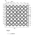
- FIG. 3 is a plan view of the first main surface 100ST of the main functional unit 10 configuring the touch panel 1 according to the first embodiment of the present invention.
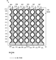
- FIG. 4 is a plan view of the second main surface 100SB of the main function unit 10 constituting the touch panel 1 according to the first embodiment of the present invention.
- 3 and 4 are views of the first main surface 100ST and the second main surface 100SB as viewed from the first main surface 100SST side. 1, 2, 3, and 4 are examples, and the first capacitance detection sub-electrode, the second capacitance detection sub-electrode, the first piezoelectric voltage detection sub-electrode, and The number of the second piezoelectric voltage detection sub-electrodes is not limited to this, and the number is appropriately determined according to the specifications of the touch panel.
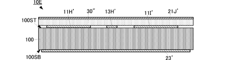
- the touch panel 1 includes a piezoelectric film 100, protective layers 30 and 40, a piezoelectric voltage detection electrode and a capacitance detection electrode formed in a pattern to be described later.
- the piezoelectric film 100 is formed of a rectangular flat film having a first main surface 100ST and a second main surface 100SB facing each other.
- the piezoelectric film 100 is made of uniaxially stretched L-type polylactic acid (PLLA).
- PLLA is a chiral polymer and its main chain has a helical structure.
- PLLA is uniaxially stretched and has piezoelectricity when the molecules are oriented.
- the piezoelectric constant of uniaxially stretched PLLA belongs to a very high class among the piezoelectric constants of various polymers.
- the draw ratio is preferably about 3 to 8 times.
- the same effect as that of uniaxial stretching can be obtained by varying the stretching ratio of each axis. For example, when a certain direction is taken as an X-axis, 8 times in that direction, and 2 times in the Y-axis direction perpendicular to that axis, the piezoelectric constant is about 4 times in the X-axis direction, The same effect can be obtained. Since a film that is simply uniaxially stretched easily tears along the direction of the stretch axis, the strength can be somewhat increased by performing biaxial stretching as described above.
- PLLA generates piezoelectricity by molecular orientation processing such as stretching, and there is no need to perform poling processing like other polymers such as PVDF and piezoelectric ceramics. That is, the piezoelectricity of PLLA that does not belong to ferroelectrics is not expressed by the polarization of ions like ferroelectrics such as PVDF and PZT, but is derived from a helical structure that is a characteristic structure of molecules. is there. For this reason, the pyroelectricity generated in other ferroelectric piezoelectric materials does not occur in PLLA. Further, PVDF or the like shows a change in piezoelectric constant over time, and in some cases, the piezoelectric constant may be significantly reduced, but the piezoelectric constant of PLLA is extremely stable over time.
- PLLA has a low dielectric constant, unlike a general ferroelectric that can obtain a high piezoelectric constant. Therefore, the electric field confinement effect between the electrode formed on first main surface 100ST and the electrode formed on second main surface 100SB is low. Thereby, if a dielectric such as a finger approaches or contacts from the outside, the capacitance is likely to change. That is, the detection sensitivity to the change in capacitance is high.
- the first main surface 100ST of the piezoelectric film 100 made of PLLA having such characteristics is provided with a plurality of first capacitance detection sub-electrodes 11A to 11F constituting capacitance detection electrodes and a piezoelectric voltage detection.
- a plurality of first piezoelectric voltage detection sub-electrodes 13A to 13L constituting the electrodes are formed in a pattern as shown in FIGS.
- the plurality of first capacitance detection sub-electrodes 11A to 11F and the plurality of first piezoelectric voltage detection sub-electrodes 13A to 13L are organic electrodes mainly composed of ITO, ZnO, polythiophene, and polyaniline as a main component.
- an organic electrode it is preferable to use any one of an organic electrode, an electrode using silver nanowires, and an electrode using carbon nanotubes.
- an electrode pattern with high translucency can be formed.
- These materials are formed by vapor deposition, sputtering, plating, or the like.
- a metal electrode other than the above-mentioned material formed by vapor deposition, sputtering, plating, or the like, or an electrode formed of silver paste can be used.
- the plurality of first capacitance detection sub-electrodes 11A to 11F have the same shape.
- the first capacitance detection sub-electrode 11A includes a plurality of wide portions 111, a plurality of narrow portions 112, and a pair of wide portions 113 for end portions.
- Each wide portion 111 is a square.
- the wide portion 111 does not necessarily have to be a square, and may be a rhombus, a parallelogram, or the like, and can have any shape required by the detection IC.
- the narrow portion 112 has a rectangular shape with a long length with respect to the width.
- the wide portion 113 for the end portion is formed of a substantially isosceles triangle.
- the plurality of wide portions 111 and the plurality of narrow portions 112 are connected so as to be alternately arranged along the extending direction of the first capacitance detection sub-electrode 11A. At this time, each wide portion 111 is connected to the narrow portion 112 so that the diagonal line of the square and the connection direction to the narrow portion 112 are parallel to each other. Further, each wide portion 111 is connected to the narrow portion 112 at a pair of apex angles forming the diagonal line.
- Wide ends 113 for end portions are provided at both ends in the extending direction of the first capacitance detection sub-electrode 11A. Both ends of the continuous electrode pattern composed of the plurality of wide portions 111 and the plurality of narrow portions 112 are connected to the wide portions 113 for the end portions by the narrow portions 112. At this time, the wide portion 113 for the end portion is connected to the narrow portion 112 at an apex angle of an isosceles triangle.
- the plurality of first capacitance detection sub-electrodes 11A to 11F are formed so as to extend along the first direction on the first main surface 100ST of the piezoelectric film 100.
- the plurality of first capacitance detection sub-electrodes 11A to 11F are formed at predetermined intervals along a second direction orthogonal to the first direction on the first main surface 100ST.
- the plurality of first capacitance detection sub-electrodes 11A to 11F are arranged so that the wide portions 111 are at the same position along the first direction, in other words, the wide portions 111 are respectively in the second direction. It is formed so that it may be arranged along.
- the first direction and the second direction are set to directions that form an angle of about 45 ° with respect to the uniaxial stretching direction 900 of the piezoelectric film 100.
- About 45 ° means an angle including about 45 ° ⁇ 10 °, for example.
- These angles are design items that should be determined as appropriate based on the overall design, such as bending detection accuracy, based on the application of the displacement sensor.
- the plurality of first piezoelectric voltage detection sub-electrodes 13A to 13L are shaped along the outer shape of the first capacitance detection sub-electrodes 11A to 11F, and are separated from the first capacitance detection sub-electrodes 11A to 11F. Is formed.
- the first piezoelectric voltage detection sub-electrode 13A is arranged along the outer diameter shape of the first capacitance detection sub-electrode 11A opposite to the first capacitance detection sub-electrode 11B.
- 1 Capacitance detection sub-electrode 11A is formed apart from it.
- the first piezoelectric voltage detection sub-electrode 13B is arranged along the outer diameter shape of the first capacitance detection sub-electrode 11A on the first capacitance detection sub-electrode 11B side. It is formed away from the electrode 11A.
- the first piezoelectric voltage detection sub-electrode 13C is arranged along the outer diameter shape of the first capacitance detection sub-electrode 11B on the first capacitance detection sub-electrode 11A side. It is formed away from the electrode 11B.
- the first piezoelectric voltage detection sub-electrodes 13B and 13C are connected to each other in the vicinity of the corners of the wide portion 111 and the wide end portion 113 of the first capacitance detection sub-electrode.
- the first piezoelectric voltage detection sub-electrode 13D is arranged along the outer diameter shape of the first capacitance detection sub-electrode 11B on the first capacitance detection sub-electrode 11C side. It is formed away from the electrode 11B.
- the first piezoelectric voltage detection sub-electrode 13E is arranged along the outer diameter shape of the first capacitance detection sub-electrode 11C on the first capacitance detection sub-electrode 11B side. It is formed away from the electrode 11C.
- the first piezoelectric voltage detection sub-electrodes 13D and 13E are connected to each other in the vicinity of the corners of the wide portion 111 and the wide end portion 113 of the first capacitance detection sub-electrode.
- the first piezoelectric voltage detection sub-electrode 13F is arranged along the outer diameter shape of the first capacitance detection sub-electrode 11C on the first capacitance detection sub-electrode 11D side. It is formed away from the electrode 11C.
- the first piezoelectric voltage detection sub-electrode 13G is arranged along the outer diameter shape of the first capacitance detection sub-electrode 11D on the first capacitance detection sub-electrode 11C side. It is formed apart from the electrode 11D.
- the first piezoelectric voltage detection sub-electrodes 13F and 13G are connected to each other in the vicinity of the corners of the wide portion 111 and the wide end portion 113 of the first capacitance detection sub-electrode.
- the first piezoelectric voltage detection sub-electrode 13H is arranged along the outer diameter shape of the first capacitance detection sub-electrode 11D on the first capacitance detection sub-electrode 11E side. It is formed apart from the electrode 11D.
- the first piezoelectric voltage detection sub-electrode 13I is arranged along the outer diameter shape of the first capacitance detection sub-electrode 11E on the first capacitance detection sub-electrode 11D side. It is formed apart from the electrode 11E.
- the first piezoelectric voltage detection sub-electrodes 13H and 13I are connected to each other in the vicinity of the corners of the wide portion 111 and the wide end portion 113 of the first capacitance detection sub-electrode.
- the first piezoelectric voltage detection sub-electrode 13J is arranged along the outer diameter shape of the first capacitance detection sub-electrode 11E on the first capacitance detection sub-electrode 11F side. It is formed apart from the electrode 11E.
- the first piezoelectric voltage detection sub-electrode 13K is arranged along the outer diameter shape of the first capacitance detection sub-electrode 11F on the first capacitance detection sub-electrode 11E side. It is formed away from the electrode 11F.
- the first piezoelectric voltage detection sub-electrodes 13J and 13K are connected to each other in the vicinity of the corners of the wide portion 111 and the wide end portion 113 of the first capacitance detection sub-electrode.
- the first piezoelectric voltage detection sub-electrode 13L is arranged along the outer diameter shape of the first capacitance detection sub-electrode 11F opposite to the first capacitance detection sub-electrode 11E. It is formed apart from the sub electrode 11F for use.
- the first piezoelectric voltage detection sub-electrodes 13A to 13K are grouped together by the routing electrode 14 and connected to an external circuit.
- the first capacitance detection sub-electrodes 11A to 11F are individually connected to the routing electrodes 12A to 12F, respectively, and connected to an external circuit via the routing electrodes 12A to 12F.
- the routing electrodes 12A to 12F and 14 are formed outside the region where the first capacitance detection sub-electrodes 11A to 11F and the first piezoelectric voltage detection sub-electrodes 13A to 13K are formed. Further, the routing electrodes 12A to 12F are formed at one end in the first direction, and the routing electrode 14 is formed at the other end in the first direction.
- a plurality of second capacitance detection sub-electrodes 21A, 21B, 21C, 21D, 21E, 21F constituting the capacitance detection electrode, and a piezoelectric voltage detection are in a pattern as shown in FIGS. Is formed.
- the plurality of second capacitance detection sub-electrodes 21A to 21F and second piezoelectric voltage detection sub-electrodes 23A to 23L are also organic electrodes mainly composed of ITO, ZnO, polythiophene, and organic electrodes mainly composed of polyaniline. It is preferable to use either an electrode using silver nanowires or an electrode using carbon nanotubes. By using these materials, an electrode pattern with high translucency can be formed. When transparency is not required, an electrode formed of silver paste, or a metal electrode formed by vapor deposition, sputtering, plating, or the like can be used.
- the plurality of second capacitance detection sub-electrodes 21A to 21F have the same shape.
- the second capacitance detection sub-electrode 21A includes a plurality of wide portions 211, a plurality of narrow portions 212, and a pair of wide portions 213 for end portions.
- Each wide portion 211 is a square.
- the wide portion 211 is not necessarily square, and may be a rhombus, a parallelogram, or the like, and can have any shape required by the detection IC.
- the narrow portion 212 has a rectangular shape with a long length with respect to the width.
- the wide portion 213 for the end portion is formed of a substantially isosceles triangle.
- the plurality of wide portions 211 and the plurality of narrow portions 212 are connected to be alternately arranged along the extending direction of the second capacitance detection sub-electrode 21A. At this time, each wide portion 211 is connected to the narrow portion 212 so that the diagonal line of the square and the connection direction to the narrow portion 212 are parallel to each other. Further, each wide portion 211 is connected to the narrow portion 212 at a pair of apex angles forming the diagonal line.
- Wide ends 213 for end portions are provided at both ends in the extending direction of the second capacitance detection sub-electrode 21A. Both ends of a continuous electrode pattern composed of a plurality of wide portions 211 and a plurality of narrow portions 212 are connected to the wide portions 213 for the end portions by the narrow portions 212. At this time, the wide portion 213 for the end portion is connected to the narrow portion 212 at an apex angle of an isosceles triangle.
- the plurality of second capacitance detection sub-electrodes 21A to 21F are formed to extend along the second direction of the second main surface 100SB of the piezoelectric film 100.
- the plurality of second capacitance detection sub-electrodes 21A to 21F are formed at predetermined intervals along a first direction orthogonal to the second direction on the second main surface 100SB.
- the plurality of second capacitance detection sub-electrodes 21A to 21F are arranged so that the wide portions 211 are at the same position along the second direction, in other words, the wide portions 211 are respectively in the first direction. It is formed so that it may be arranged along.
- the plurality of second capacitance detection sub-electrodes 21A to 21F are configured such that the wide portions 212 do not face the wide portions 111 of the first capacitance detection sub-electrodes 11A to 11F via the piezoelectric film 100. Is formed.
- the wide portions 212 constituting the plurality of second capacitance detection sub-electrodes 21A to 21F constitute the first capacitance detection sub-electrodes 11A to 11F.
- the second capacitance detection sub-electrodes 21A to 21F are formed so as not to overlap the wide portions 111 to be performed.
- the plurality of first capacitance detection sub-electrodes 11A to 11F and the plurality of second capacitance detection sub-electrodes 21A to 21F are piezoelectric only at the narrow portions 112 and 212. It faces through the film 100.
- the wide portions 211 constituting the plurality of second capacitance detection sub-electrodes 21A to 21F and the first capacitance detection sub-electrodes 11A to 11F are constituted.
- the first capacitance detection sub-electrodes 11A to 11F and the second capacitance detection sub-electrodes 21A to 21F are formed so that gaps with a predetermined width are formed between the wide portions 111.
- the width of the gap is set so that the first piezoelectric voltage detection sub-electrodes 13A to 13K formed on the first main surface 100ST are within the gap when viewed from the first main surface 100ST side. ing.
- the plurality of second piezoelectric voltage detection sub-electrodes 23A to 23L are shaped along the outer diameter of the second capacitance detection sub-electrodes 21A to 21F, and are connected to the second capacitance detection sub-electrodes 21A to 21F. They are spaced apart.
- the second piezoelectric voltage detection sub-electrode 23A is arranged along the outer diameter shape of the second capacitance detection sub-electrode 21A opposite to the second capacitance detection sub-electrode 21B. 2 It is formed apart from the capacitance detecting sub-electrode 21A.
- the second piezoelectric voltage detection sub-electrode 23B is arranged along the outer diameter shape of the second capacitance detection sub-electrode 21A on the second capacitance detection sub-electrode 21B side. It is formed away from the electrode 21A.
- the second piezoelectric voltage detection sub-electrode 23C extends along the outer diameter shape of the second capacitance detection sub-electrode 21B on the second capacitance detection sub-electrode 21A side. It is formed away from the electrode 21B.
- the second piezoelectric voltage detection sub-electrodes 23B and 23C are connected to each other in the vicinity of the corners of the wide portion 211 and the wide end portion 213 of the second capacitance detection sub-electrode.
- the second piezoelectric voltage detection sub-electrode 23D is arranged along the outer diameter shape of the second capacitance detection sub-electrode 21B on the second capacitance detection sub-electrode 21C side. It is formed away from the electrode 21B.
- the second piezoelectric voltage detection sub-electrode 23E is arranged along the outer diameter shape of the second capacitance detection sub-electrode 21C on the second capacitance detection sub-electrode 21B side. It is formed away from the electrode 21C.
- the second piezoelectric voltage detection sub-electrodes 23D and 23E are connected to each other in the vicinity of the corners of the wide portion 211 and the wide end portion 213 of the second capacitance detection sub-electrode.
- the second piezoelectric voltage detection sub-electrode 23F is arranged along the outer diameter shape of the second capacitance detection sub-electrode 21C on the second capacitance detection sub-electrode 21D side. It is formed away from the electrode 21C.
- the second piezoelectric voltage detection sub-electrode 23G is arranged along the outer diameter shape of the second capacitance detection sub-electrode 21D on the second capacitance detection sub-electrode 21C side. It is formed away from the electrode 21D.
- the second piezoelectric voltage detection sub-electrodes 23F and 23G are connected to each other in the vicinity of the corners of the wide portion 211 and the wide end portion 213 of the second capacitance detection sub-electrode.
- the second piezoelectric voltage detection sub-electrode 23H extends along the outer diameter shape of the second capacitance detection sub-electrode 21D on the second capacitance detection sub-electrode 21E side. It is formed away from the electrode 21D.
- the second piezoelectric voltage detection sub-electrode 23I is arranged along the outer diameter shape of the second capacitance detection sub-electrode 21E on the second capacitance detection sub-electrode 21D side. It is formed away from the electrode 21E.
- the second piezoelectric voltage detection sub-electrodes 23H and 23I are connected to each other in the vicinity of the corners of the wide portion 211 and the wide end portion 213 of the second capacitance detection sub-electrode.
- the second piezoelectric voltage detection sub-electrode 23J is arranged along the outer diameter shape of the second capacitance detection sub-electrode 21E on the second capacitance detection sub-electrode 21F side. It is formed away from the electrode 21E.
- the second piezoelectric voltage detection sub-electrode 23K is arranged along the outer diameter shape of the second capacitance detection sub-electrode 21F on the second capacitance detection sub-electrode 21E side. It is formed away from the electrode 21F.
- the second piezoelectric voltage detection sub-electrodes 23J and 23K are connected to each other in the vicinity of the corners of the wide portion 211 and the wide end portion 213 of the second capacitance detection sub-electrode.
- the second piezoelectric voltage detection sub-electrode 23L is arranged along the outer diameter shape of the second capacitance detection sub-electrode 21F opposite to the second capacitance detection sub-electrode 21E. It is formed apart from the sub electrode 21F for use.
- the second piezoelectric voltage detection sub-electrodes 23A to 23L formed on the second main surface 100SB and the first piezoelectric voltage detection sub-electrodes 13A to 13K formed on the first main surface 100ST are wide portions 211 and 213, respectively. Are formed so as to face each other through the piezoelectric film 100 over substantially the entire length in a gap seen from the first main surface 100ST side generated between the wide film portions 111 and 113.
- the second piezoelectric voltage detection sub-electrode 23A includes a wide portion 213 for the end of the second capacitance detection sub-electrode 21A and a first capacitance detection sub-electrode 11A.
- the first piezoelectric voltage detection sub-electrode 13A is opposed to the wide end portion 113 for the end portion.
- the second piezoelectric voltage detection sub-electrode 23A includes a wide portion 211 of the second capacitance detection sub-electrode 21A and a wide portion 113 for the ends of the first capacitance detection sub-electrodes 11A and 11B.
- the first piezoelectric voltage detection sub-electrodes 13B and 13C are opposed to each other.
- the other portions of the second piezoelectric voltage detection sub-electrode 23A are similarly opposed to the first piezoelectric voltage detection sub-electrodes 13D to 13L, and the other second piezoelectric voltage detection sub-electrodes 23A to 13L.
- the electrodes 23B to 23L also face the first piezoelectric voltage detection sub-electrodes 13A to 13L, respectively.
- the second piezoelectric voltage detection sub-electrodes 23A to 23K are grouped together by the routing electrode 24 and connected to an external circuit.
- the second capacitance detection sub-electrodes 21A to 21F are individually connected to the routing electrodes 22A to 22F, and are connected to an external circuit via the routing electrodes 22A to 22F.
- the routing electrodes 22A to 22F and 24 are formed outside the formation area of the second capacitance detection sub-electrodes 21A to 21F and the second piezoelectric voltage detection sub-electrodes 23A to 23K. Further, the routing electrodes 22A to 22F are formed at one end in the second direction, and the routing electrode 24 is formed at the other end in the second direction.
- the main functional unit 10 of the touch panel 1 is configured by the piezoelectric film 100 on which ⁇ 23L is formed.
- the protective layer 30 is disposed so as to cover.
- the protective layer 30 has an insulating property and is formed of a light-transmitting material. Note that in the case where translucency is not required, the material is not particularly limited as long as it has insulating properties.
- the entire electrode pattern formation region of the second capacitance detection sub-electrodes 21A to 21F and the second piezoelectric voltage detection sub-electrodes 23A to 23L is formed.
- a protective layer 40 is disposed so as to cover.
- the protective layer 40 is also made of a material having insulating properties and translucency. Note that in the case where translucency is not required, the material is not particularly limited as long as it has insulating properties.
- the protective layers 30 and 40 may be made of polyethylene terephthalate PET, polyethylene naphthalate PEN, polypropylene PP, or the like, and may be formed in a shape (thickness or the like) that does not inhibit the bending of the piezoelectric film 100.
- the touch panel 1 having the above structure detects the touch position and the push-in amount as shown below.
- the routing electrodes 12A to 12F and 22A to 22F for detecting the capacitance are connected to the capacitance detecting circuit.
- the lead electrodes 14 and 24 for detecting the piezoelectric voltage are connected to a piezoelectric voltage detecting circuit.
- the touch position is detected by the following principle.
- a so-called projection type mutual capacitance method touch position detection concept is used, and a detailed description of the detection concept is omitted. Therefore, the touch position detection concept will be schematically described below.
- a drive signal is applied between the first capacitance detection sub-electrodes 11A to 11F and the second capacitance detection sub-electrodes 21A to 21F via the routing electrodes 12A to 12F and the routing electrodes 22A to 22F. Is done.
- the first capacitance detection sub-electrodes 11A to 11F extend in the first direction and are arranged at predetermined intervals along the second direction. Since 21A to 21F extend in the second direction and are arranged at predetermined intervals along the first direction, the first capacitance detection sub-electrodes 11A to 11F and the second capacitance detection sub-electrode The positions at which 21A to 21F face each other through the piezoelectric film 100, in other words, the positions at which an electric field is generated and a detection current flows, are the first capacitance detection sub-electrode and the second capacitance that constitute the facing position. Two-dimensional coordinates can be detected from the combination with the detection sub-electrode.
- the touch position can be detected.
- first capacitance detection sub-electrodes 11A to 11F and the second capacitance detection sub-electrodes 21A to 21F of the present embodiment are viewed along a direction orthogonal to the first main surface 100ST which is an operation surface.
- first capacitance detection sub-electrodes 11A to 11F and the second capacitance detection are arranged so as to face each other at the narrow portions 112 and 212 and not to overlap each other at the wide portions 111 and 112. Electric field changes due to the touch of the finger are likely to occur on both the sub electrodes 21A to 21F. Thereby, the detection sensitivity of a touch can be improved.
- the piezoelectric film 100 is PLLA, the dielectric constant for forming the capacitance is low, and it is easily affected by the outside. Thereby, an electric field change due to a finger touch is more likely to occur, and the touch detection sensitivity can be further improved.
- FIG. 5 is a diagram for explaining the push-in amount detection function of the main function unit 10 according to the first embodiment of the present invention.
- FIG. 5A shows a state where the pushing force is not involved
- FIG. 5B shows a state where the pushing force by the finger is concerned.
- FIG. 6A is a graph showing the correlation between the push-in amount and the detection voltage
- FIG. 6B is a waveform diagram of the push-in detection voltage of the main function unit 10 according to the first embodiment of the present invention. It is.
- the main functional unit 10 of the touch panel 1 is attached to one main surface of the flat elastic body 50 so that the flat surfaces are in close contact with each other.
- the elastic body 50 is made of glass, acrylic, polycarbonate, or the like.
- the elastic body 50 is not limited to the material described here, and an appropriate material may be selected according to the use conditions. Moreover, what is necessary is just to select an appropriate surface according to use conditions also about the surface which bonds the main function part 10 of the touch panel 1.
- the opposite ends of the elastic body 50 are supported by the support body 501. That is, in the case of the touch panel 1, both ends in the first direction of the touch panel 1 are fixed. In this state, since the elastic body 50 is not bent and no stress is applied to the piezoelectric film 100, no charge is generated.
- the elastic body 50 when the surface of the elastic body 50 is pressed with a finger 510, a pressing force as shown by a thick arrow 520 is applied to the elastic body 50.
- the elastic body 50 is curved so as to swell toward the arrangement surface side of the main function unit 10.
- the piezoelectric film 100 of the main functional unit 10 is stretched substantially along the first direction, and a tensile stress as indicated by a thick arrow 530 is generated. Due to this stress, the piezoelectric film 100 is polarized into the first main surface 100ST and the second main surface 100SB.
- the first piezoelectric voltage detection sub-electrodes 13A to 13L are formed on the first main surface 100ST, and the second piezoelectric voltage detection sub-electrodes 23A to 23L are formed on the second main surface 100SB.
- a potential difference is generated between the first piezoelectric voltage detection sub-electrodes 13A to 13L and the second piezoelectric voltage detection sub-electrodes 23A to 23L. Therefore, by detecting this potential difference, that is, the piezoelectric voltage, it is possible to detect pressing by a finger, in other words, pressing by a finger touch.
- the detection voltage (piezoelectric voltage) changes linearly as the film is stretched according to the amount of pressing. Therefore, the push-in amount can be detected by measuring the detection voltage value with the piezoelectric voltage detection circuit. That is, it is possible to accurately detect whether the operator has touched the operation surface lightly or pressed it strongly.
- the detection voltage by the piezoelectric film 100 is normally generated at the moment when the stress is generated, and the detection voltage value is rapidly decreased with the leakage of electric charge due to the piezoelectric effect.
- the detection voltage value can be maintained for a predetermined time as shown in FIG. 6B. As a result, the detected voltage value can be more reliably measured and the push-in amount can be detected. Similar effects can be obtained by integrating signals in a software manner instead of the detection circuit and the integration circuit having a large input impedance.
- the touch position and the push-in amount can be obtained simply by forming the capacitance detection electrode and the piezoelectric voltage detection electrode on both opposing surfaces of one piezoelectric film 100. Pressure) can be detected simultaneously. Furthermore, a touch panel with high translucency can be realized.
- PLLA is a polymer and has flexibility, so that it is not damaged by a large displacement unlike piezoelectric ceramics. Therefore, even if the displacement amount is large, the displacement amount can be reliably detected.
- the protective layers 30 and 40 are simply disposed.
- the elastic body 50 such as an acrylic plate having a high elastic modulus is provided on the first main surface 100ST side of the main functional unit 10.
- the protective layer 40 may be disposed only on the second main surface 100SB side.
- the protective layers 30 and 40 may be provided so that the surface of the protective layer 40 on the side opposite to the main functional portion 10 has adhesiveness. Furthermore, by making this adhesiveness weakly adhesive, it is possible to realize a touch panel that can be mounted or removed depending on the place of use.
- FIG. 7 is a diagram for explaining a first manufacturing method of the touch panel 1.
- FIG. 8 is a diagram for explaining a second manufacturing method of the touch panel 1. In FIG. 7 and FIG. 8, detailed electrode patterns are not shown, but are simply shown.
- the first capacitance detection sub-electrodes 11A to 11F, the first piezoelectric voltage detection sub-electrodes 13A to 13L, and the routing electrode are formed on the first main surface 100ST of the piezoelectric film 100.
- 12A to 12F and 14 are formed.
- the second capacitance detection sub-electrodes 21A to 21F, the second piezoelectric voltage detection sub-electrodes 23A to 23L, and the routing electrodes 22A to 22F and 24 are formed on the second main surface 100SB of the piezoelectric film 100. .
- the order of electrode formation on the first main surface 100ST and the second main surface 100SB may be reversed. Thereby, the main function unit 10 is configured first.
- the protective layer 30 is disposed on the first main surface 100ST side of the piezoelectric film 100 in the main function unit 10. And the protective layer 40 is arrange
- the first capacitance detection sub-electrodes 11A to 11F, the first piezoelectric voltage detection sub-electrodes 13A to 13L, and the routing electrodes 12A to 12F are formed on one main surface of the protective layer 30. , 14 are formed.
- the second capacitance detection sub-electrodes 21A to 21F, the second piezoelectric voltage detection sub-electrodes 23A to 23L, and the routing electrodes 22A to 22F, 24 are formed on one main surface of the protective layer 40.
- the protective layer 30 on which the electrode pattern is formed is adhered to the first main surface 100ST of the piezoelectric film 100 so that the electrode pattern surface is on the piezoelectric film 100 side. Further, the protective layer 40 on which the electrode pattern is formed is adhered to the second main surface 100SB of the piezoelectric film 100 so that the electrode pattern surface is on the piezoelectric film 100 side. Thereby, the touch panel 1 is formed.
- a touch panel can be formed by an easy process as compared with the manufacturing method of FIG. This is because the surface of the PLLA is inactive, and thus when the electrode pattern is formed, a process for improving the adhesion of the electrode is required.
- the protective layers 30 and 40 are formed of PET or PEN, electrode formation is easy. Therefore, the touch panel 1 can be easily manufactured by using the manufacturing method of FIG.
- any treatment is performed on the surface of PLLA, the light transmittance of PLLA may be lowered. Therefore, if the use application places importance on light transmittance, it is better to use the manufacturing method of FIG. .
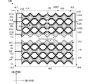
- FIG. 9 is a plan view of the first main surface 100ST of the main functional unit 10A constituting the touch panel 1A according to the second embodiment of the present invention.
- FIG. 10 is a plan view of the second main surface 100SB of the main functional unit 10A constituting the touch panel 1A according to the second embodiment of the present invention.
- the touch panel 1A of the present embodiment is different from the touch panel 1 shown in the first embodiment only in the fixing structure, the uniaxial stretching direction of the piezoelectric film 100, and the shape of the piezoelectric voltage detection sub-electrode, Other configurations are the same. Therefore, below, only a different part from the touch panel 1 shown in 1st Embodiment is demonstrated concretely.
- the touch panel 1A of the present embodiment has a structure in which the four sides of the piezoelectric film 100 are fixed. At this time, the piezoelectric film 100 is formed such that the uniaxial stretching direction 900 is orthogonal to the pair of fixed sides and parallel to the other pair of fixed sides.
- first capacitance detection sub-electrodes 11A to 11F are formed on the first main surface 100ST of the piezoelectric film 100. As shown in FIG. The first capacitance detection sub-electrodes 11A to 11F have the same structure as that of the first embodiment, but the extending direction of the first capacitance detection sub-electrodes 11A to 11F is a uniaxial extension direction 900 (first direction). ) To be parallel to each other.
- the first piezoelectric voltage detection sub-electrodes 131A and 132A are arranged along the outer diameter of the first capacitance detection sub-electrode 11A opposite to the first capacitance detection sub-electrode 11B. It is formed apart from the capacitance detection sub-electrode 11A.
- the first piezoelectric voltage detection sub-electrodes 131A and 132A are separated at an intermediate point along the first direction, and one end side along the first direction from the separation point 150 becomes the first piezoelectric voltage detection sub-electrode 131A.
- the other end side along the first direction from the separation point 150 is the first piezoelectric voltage detection sub-electrode 132A.
- the first piezoelectric voltage detection sub-electrodes 131B and 132B are arranged along the outer diameter shape on the first capacitance detection sub-electrode 11B side in the first capacitance detection sub-electrode 11A. It is formed apart from the sub electrode 11A for use.
- the first piezoelectric voltage detection sub-electrodes 131B and 132B are separated at an intermediate point along the first direction, and one end side along the first direction from the separation point 150 becomes the first piezoelectric voltage detection sub-electrode 131B.
- the other end side along the first direction from the separation point 150 is the first piezoelectric voltage detection sub-electrode 132B.
- the first piezoelectric voltage detection sub-electrodes 131C and 132C are arranged along the outer diameter shape of the first capacitance detection sub-electrode 11B on the first capacitance detection sub-electrode 11A side. It is formed away from the sub electrode 11B for use.
- the first piezoelectric voltage detection sub-electrodes 131C and 132C are separated at an intermediate point along the first direction, and one end side along the first direction from the separation point 150 becomes the first piezoelectric voltage detection sub-electrode 131C.
- the other end along the first direction from the separation point 150 is the first piezoelectric voltage detecting sub-electrode 132C.
- the first piezoelectric voltage detection sub-electrodes 131B and 131C are connected to each other in the vicinity of the corners of the wide portion 111 and the wide end portion 113 of the first capacitance detection sub-electrode.
- the first piezoelectric voltage detection sub-electrodes 132B and 132C are connected to each other in the vicinity of the corners of the wide portion 111 and the wide end portion 113 of the first capacitance detection sub-electrode.
- the first piezoelectric voltage detection sub-electrodes 131D and 132D are arranged along the outer diameter shape of the first capacitance detection sub-electrode 11B on the first capacitance detection sub-electrode 11C side. It is formed away from the sub electrode 11B for use.
- the first piezoelectric voltage detection sub-electrodes 131D and 132D are separated at an intermediate point along the first direction, and one end side along the first direction from the separation point 150 is the first piezoelectric voltage detection sub-electrode 131D.
- the other end side along the first direction from the separation point 150 is the first piezoelectric voltage detection sub-electrode 132D.
- the first piezoelectric voltage detection sub-electrodes 131E and 132E are arranged along the outer diameter shape of the first capacitance detection sub-electrode 11C on the first capacitance detection sub-electrode 11B side. It is formed away from the sub electrode 11C.
- the first piezoelectric voltage detection sub-electrodes 131E and 132E are separated at an intermediate point along the first direction, and one end side along the first direction from the separation point 150 becomes the first piezoelectric voltage detection sub-electrode 131E.
- the other end side in the first direction from the separation point 150 is the first piezoelectric voltage detection sub-electrode 132E.
- the first piezoelectric voltage detection sub-electrodes 131D and 131E are connected to each other in the vicinity of the corners of the wide portion 111 and the wide end portion 113 of the first capacitance detection sub-electrode.
- the first piezoelectric voltage detection sub-electrodes 132D and 132E are connected to each other in the vicinity of the corners of the wide portion 111 and the wide end portion 113 of the first capacitance detection sub-electrode.
- the first piezoelectric voltage detection sub-electrodes 131A, 131B, 131C, 131D, and 131E are grouped together by the lead-out electrode 141, and are connected to an external circuit from one end side in the first direction of the piezoelectric film 100.
- the first piezoelectric voltage detection sub-electrodes 132A, 132B, 132C, 132D, and 132E are grouped together by the lead-out electrode 142, and are connected to the external circuit from the other end side in the first direction of the piezoelectric film 100.
- a piezoelectric voltage detection subelectrode is provided between the first capacitance detection subelectrode 11C and the first capacitance detection subelectrode 11D, which is a central region along the second direction of the first main surface 100ST. Not formed.
- the first piezoelectric voltage detection sub-electrodes 131H and 132H are arranged along the outer diameter shape of the first capacitance detection sub-electrode 11D on the first capacitance detection sub-electrode 11E side. It is formed away from the sub electrode 11D for use.
- the first piezoelectric voltage detection sub-electrodes 131H and 132H are separated at an intermediate point along the first direction, and one end side along the first direction from the separation point 150 becomes the first piezoelectric voltage detection sub-electrode 131H.
- the other end side along the first direction from the separation point 150 is the first piezoelectric voltage detection sub-electrode 132H.
- the first piezoelectric voltage detection sub-electrodes 131I and 132I are arranged along the outer diameter shape of the first capacitance detection sub-electrode 11E on the first capacitance detection sub-electrode 11D side. It is formed apart from the sub electrode 11E for use.
- the first piezoelectric voltage detection sub-electrodes 131I and 132I are separated at an intermediate point along the first direction, and one end side along the first direction from the separation point 150 becomes the first piezoelectric voltage detection sub-electrode 131I.
- the other end side along the first direction from the separation point 150 is the first piezoelectric voltage detection sub-electrode 132I.
- the first piezoelectric voltage detection sub-electrodes 131H and 131I are connected to each other in the vicinity of the corners of the wide portion 111 and the wide end portion 113 of the first capacitance detection sub-electrode.
- the first piezoelectric voltage detection sub-electrodes 132H and 132I are connected to each other in the vicinity of the corners of the wide portion 111 and the wide end portion 113 of the first capacitance detection sub-electrode.
- the first piezoelectric voltage detection sub-electrodes 131J and 132J are arranged along the outer diameter shape of the first capacitance detection sub-electrode 11E on the first capacitance detection sub-electrode 11F side. It is formed apart from the sub electrode 11E for use.
- the first piezoelectric voltage detection sub-electrodes 131J and 132J are separated at an intermediate point along the first direction, and one end side along the first direction from the separation point 150 becomes the first piezoelectric voltage detection sub-electrode 131J.
- the other end side along the first direction from the separation point 150 is the first piezoelectric voltage detection sub-electrode 132J.
- the first piezoelectric voltage detection sub-electrodes 131K and 132K are arranged along the outer diameter shape of the first capacitance detection sub-electrode 11F on the first capacitance detection sub-electrode 11E side. It is formed apart from the sub electrode 11F for use.
- the first piezoelectric voltage detection sub-electrodes 131K and 132K are separated at an intermediate point along the first direction, and one end side along the first direction from the separation point 150 becomes the first piezoelectric voltage detection sub-electrode 131K.
- the other end side along the first direction from the separation point 150 is the first piezoelectric voltage detection sub-electrode 132K.
- the first piezoelectric voltage detection sub-electrodes 131J and 131K are connected to each other in the vicinity of the corners of the wide portion 111 and the wide end portion 113 of the first capacitance detection sub-electrode.
- the first piezoelectric voltage detection sub-electrodes 132J and 132K are connected to each other in the vicinity of the corners of the wide portion 111 and the wide end portion 113 of the first capacitance detection sub-electrode.
- the first piezoelectric voltage detection sub-electrodes 131L and 132L are arranged along the outer diameter of the first capacitance detection sub-electrode 11F on the opposite side of the first capacitance detection sub-electrode 11E. It is formed away from the capacitance detection sub-electrode 11F.
- the first piezoelectric voltage detection sub-electrodes 131L and 132L are separated at an intermediate point along the first direction, and one end side along the first direction from the separation point 150 becomes the first piezoelectric voltage detection sub-electrode 131L.
- the other end side along the first direction from the separation point 150 is the first piezoelectric voltage detection sub-electrode 132L.
- the first piezoelectric voltage detection sub-electrodes 131H, 131I, 131J, 131K, and 131L are gathered together by a lead-out electrode 143, and are connected to an external circuit from one end side in the first direction of the piezoelectric film 100.
- the first piezoelectric voltage detection sub-electrodes 132H, 132I, 132J, 132K, and 132L are grouped together by the lead-out electrode 144, and are connected to the external circuit from the other end side in the first direction of the piezoelectric film 100.
- second capacitance detection sub-electrodes 21A to 21F are formed on the second main surface 100SB of the piezoelectric film 100, as shown in FIG. 10, second capacitance detection sub-electrodes 21A to 21F are formed.
- the second capacitance detection sub-electrodes 21A to 21F have the same structure as that of the first embodiment, but the extending direction of the second capacitance detection sub-electrodes 21A to 21F is orthogonal to the uniaxial extension direction 900. To be formed.
- the second piezoelectric voltage detection sub-electrodes 231A and 232A are arranged along the outer diameter of the second capacitance detection sub-electrode 21A on the opposite side of the second capacitance detection sub-electrode 21B. It is formed apart from the capacitance detection sub-electrode 21A.
- the second piezoelectric voltage detection sub-electrodes 231A and 232A are separated at an intermediate point along the second direction, and one end side along the second direction from the separation point 150 becomes the second piezoelectric voltage detection sub-electrode 231A.
- the other end side along the second direction from the separation point 150 is the second piezoelectric voltage detection sub-electrode 232A.
- the second piezoelectric voltage detection sub-electrodes 231B and 232B detect the second capacitance detection along the outer diameter shape of the second capacitance detection sub-electrode 21B on the second capacitance detection sub-electrode 21B side. It is formed away from the sub electrode 21A for use.
- the second piezoelectric voltage detection sub-electrodes 231B and 232B are separated at an intermediate point along the second direction, and one end side along the second direction from the separation point 150 becomes the second piezoelectric voltage detection sub-electrode 231B.
- the other end side along the second direction from the separation point 150 is the second piezoelectric voltage detection sub-electrode 232B.
- the second piezoelectric voltage detection sub-electrodes 231C and 232C detect the second capacitance detection along the outer diameter shape of the second capacitance detection sub-electrode 21B on the second capacitance detection sub-electrode 21A side. It is formed away from the sub electrode 21B.
- the second piezoelectric voltage detection sub-electrodes 231C and 232C are separated at an intermediate point along the second direction, and one end side along the second direction from the separation point 150 becomes the second piezoelectric voltage detection sub-electrode 231C.
- the other end side along the second direction from the separation point 150 is the second piezoelectric voltage detection sub-electrode 232C.
- the second piezoelectric voltage detection sub-electrodes 231B and 231C are connected to each other in the vicinity of the corners of the wide portion 211 and the wide end portion 213 of the second capacitance detection sub-electrode.
- the second piezoelectric voltage detection sub-electrodes 232B and 232C are connected to each other in the vicinity of the corners of the wide portion 211 and the wide end portion 213 of the second capacitance detection sub-electrode.
- the second piezoelectric voltage detection sub-electrodes 231D and 232D detect the second capacitance detection along the outer diameter shape of the second capacitance detection sub-electrode 21B on the second capacitance detection sub-electrode 21C side. It is formed away from the sub electrode 21B.
- the second piezoelectric voltage detection sub-electrodes 231D and 232D are separated at an intermediate point along the second direction, and one end side along the second direction from the separation point 150 is the second piezoelectric voltage detection sub-electrode 231D. The other end side along the second direction from the separation point 150 is the second piezoelectric voltage detection sub-electrode 232D.
- the second piezoelectric voltage detection sub-electrodes 231E and 232E detect the second capacitance detection along the outer diameter shape of the second capacitance detection sub-electrode 21B on the second capacitance detection sub-electrode 21B side. It is formed apart from the sub electrode 21C for use.
- the second piezoelectric voltage detection sub-electrodes 231E and 232E are separated at an intermediate point along the second direction, and one end side along the second direction from the separation point 150 becomes the second piezoelectric voltage detection sub-electrode 231E.
- the other end side along the second direction from the separation point 150 is the second piezoelectric voltage detection sub-electrode 232E.
- the second piezoelectric voltage detection sub-electrodes 231D and 231E are connected to each other in the vicinity of the corners of the wide portion 211 and the wide end portion 213 of the second capacitance detection sub-electrode.
- the second piezoelectric voltage detection sub-electrodes 232D and 232E are connected to each other in the vicinity of the corners of the wide portion 211 and the wide end portion 213 of the second capacitance detection sub-electrode.
- the second piezoelectric voltage detection sub-electrodes 231A, 231B, 231C, 231D, and 231E are gathered together by the lead-out electrode 241 and connected to an external circuit from one end side in the second direction of the piezoelectric film 100.
- the second piezoelectric voltage detection sub-electrodes 232A, 232B, 232C, 232D, and 232E are gathered together by the lead-out electrode 242, and are connected to the external circuit from the other end side of the piezoelectric film 100 in the second direction.
- the second piezoelectric voltage detection sub-electrodes 231H and 232H detect the second capacitance detection along the outer diameter shape of the second capacitance detection sub-electrode 21D on the second capacitance detection sub-electrode 21E side. It is formed apart from the sub electrode 21D for use.
- the second piezoelectric voltage detection sub-electrodes 231H and 232H are separated at an intermediate point along the second direction, and one end side along the second direction from the separation point 150 becomes the second piezoelectric voltage detection sub-electrode 231H.
- the other end side in the second direction from the separation point 150 is the second piezoelectric voltage detection sub-electrode 232H.
- the second piezoelectric voltage detection sub-electrodes 231I and 232I detect the second capacitance detection along the outer diameter shape of the second capacitance detection sub-electrode 21E on the second capacitance detection sub-electrode 21D side. It is formed apart from the sub electrode 21E for use.
- the second piezoelectric voltage detection sub-electrodes 231I and 232I are separated at an intermediate point along the second direction, and one end side along the second direction from the separation point 150 becomes the second piezoelectric voltage detection sub-electrode 231I.
- the other end side along the second direction from the separation point 150 is the second piezoelectric voltage detection sub-electrode 232I.
- the second piezoelectric voltage detection sub-electrodes 231H and 231I are connected to each other in the vicinity of the corners of the wide portion 211 and the wide end portion 213 of the second capacitance detection sub-electrode.
- the second piezoelectric voltage detection sub-electrodes 232H and 232I are connected to each other in the vicinity of the corners of the wide portion 211 and the wide end portion 213 of the second capacitance detection sub-electrode.
- the second piezoelectric voltage detection sub-electrodes 231J and 232J detect the second capacitance detection along the outer diameter shape of the second capacitance detection sub-electrode 21E on the second capacitance detection sub-electrode 21F side. It is formed apart from the sub electrode 21E for use.
- the second piezoelectric voltage detection sub-electrodes 231J and 232J are separated at an intermediate point along the second direction, and one end side along the second direction from the separation point 150 is the second piezoelectric voltage detection sub-electrode 231J. The other end side along the second direction from the separation point 150 is the second piezoelectric voltage detection sub-electrode 232J.
- the second piezoelectric voltage detection sub-electrodes 231K and 232K detect the second capacitance detection along the outer diameter shape of the second capacitance detection sub-electrode 21F on the second capacitance detection sub-electrode 21E side. It is formed apart from the sub electrode 21F for use.
- the second piezoelectric voltage detection sub-electrodes 231K and 232K are separated at an intermediate point along the second direction, and one end side along the second direction from the separation point 150 becomes the second piezoelectric voltage detection sub-electrode 231K.
- the other end side along the second direction from the separation point 150 is the second piezoelectric voltage detection sub-electrode 232K.
- the second piezoelectric voltage detection sub-electrodes 231J and 231K are connected to each other in the vicinity of the corners of the wide portion 211 and the wide end portion 213 of the second capacitance detection sub-electrode.
- the second piezoelectric voltage detection sub-electrodes 232J and 232K are connected to each other in the vicinity of the corners of the wide portion 211 and the wide end portion 213 of the second capacitance detection sub-electrode.
- the second piezoelectric voltage detection sub-electrodes 231L and 232L are arranged along the outer diameter of the second capacitance detection sub-electrode 21F on the opposite side of the second capacitance detection sub-electrode 21E. It is formed away from the capacitance detection sub-electrode 21F.
- the second piezoelectric voltage detection sub-electrodes 231L and 232L are separated at an intermediate point along the second direction, and one end side along the first direction from the separation point 150 becomes the second piezoelectric voltage detection sub-electrode 231L.
- the other end side along the first direction from the separation point 150 is the second piezoelectric voltage detection sub-electrode 232L.
- the second piezoelectric voltage detection sub-electrodes 231H, 231I, 231J, 231K, and 231L are gathered together by a lead-out electrode 243, and are connected to an external circuit from one end side in the second direction of the piezoelectric film 100.
- the second piezoelectric voltage detection sub-electrodes 232H, 232I, 232J, 232K, and 232L are gathered together by the lead-out electrode 244, and are connected to the external circuit from the other end side in the second direction of the piezoelectric film 100.
- Ar1, Ar2, Ar3, Ar4 can be detected individually.
- the piezoelectric voltage in the first partial region Ar1 is the first piezoelectric voltage detecting sub-electrode 131A, 131B, 131C, 131D, 131E on the first main surface 100ST and the second piezoelectric voltage detecting sub-electrode 231A on the second main surface 100SB. , 231B, 231C, 231D, and 231E.
- the piezoelectric voltage in the second partial area Ar2 is the first piezoelectric voltage detecting sub-electrodes 132A, 132B, 132C, 132D, 132E on the first main surface 100ST and the second piezoelectric voltage detecting sub-electrode 231H on the second main surface 100SB. , 231I, 231J, 231K, and 231L.
- the piezoelectric voltage in the third partial region Ar3 is the first piezoelectric voltage detecting sub-electrode 131H, 131I, 131J, 131K, 131L on the first main surface 100ST and the second piezoelectric voltage detecting sub-electrode 232A on the second main surface 100SB. , 232B, 232C, 232D, and 232E.
- the piezoelectric voltage in the fourth partial region Ar4 is the first piezoelectric voltage detecting sub-electrodes 132H, 132I, 132J, 132K, 132L on the first main surface 100ST and the second piezoelectric voltage detecting sub-electrode 232H on the second main surface 100SB. , 232I, 232J, 232K, and 232L.
- each of the partial areas Ar1, Ar2, Ar3, Ar4 has two orthogonal sides fixed, and the other two sides orthogonal to the main surface. It becomes a structure which can be bent in the direction to be. Accordingly, when the operator presses the operation surface (first main surface side) with a finger, each of the partial regions Ar1, Ar2, Ar3, Ar4 is extended to both along substantially the diagonal lines of the two orthogonal sides ( (Or it can be shrunk).
- the uniaxial stretching direction and the first direction of the piezoelectric film 100 are parallel as described above, the piezoelectric voltage due to such displacement is effectively detected in each of the partial regions Ar1, Ar2, Ar3, Ar4. can do.
- the amount of pressing as the touch panel 1A can be detected by performing arithmetic operations by combining these piezoelectric voltages. Can do.
- the first partial region Ar1 when a positive potential is detected on the first piezoelectric voltage detection sub-electrodes 131A, 131B, 131C, 131D, and 131E on the first main surface 100ST, in the second partial region Ar2, A negative potential is detected on the first piezoelectric voltage detection sub-electrodes 132A, 132B, 132C, 132D, 132E on the first main surface 100ST, and the first piezoelectric voltage detection on the first main surface 100ST is detected in the third partial region Ar3. Negative potentials are detected at the sub-electrodes 131H, 131I, 131J, 131K, and 131L.
- the first piezoelectric voltage detection sub-electrodes 132H, 132I, 132J, 132K A positive potential is detected at 132L.
- the relationship of the sign of the generated potential is almost constant regardless of the pressed position. Whether the voltages generated in the four regions are connected in a parallel relationship or a serial relationship can be selected as appropriate, and may be properly selected depending on the performance of the detection circuit and the usage environment. For example, when importance is attached to the amount of generated charge, it is preferable to connect in parallel, and when importance is attached to the magnitude of the generated potential, it may be connected in series.
- the pressing amount can be detected together with the touch position.
- FIG. 11 is a plan view of the first main surface 100ST of the main function unit 10B constituting the touch panel 1B according to the third embodiment of the present invention.
- FIG. 12 is a plan view of the second main surface 100SB of the main function unit 10B constituting the touch panel 1B according to the third embodiment of the present invention.
- the touch panel 1B of the present embodiment is different from the touch panel 1A shown in the second embodiment only in the shape of the piezoelectric voltage detection sub-electrode, and the other configurations are the same. Therefore, below, only a different part from the touch panel 1A shown in 2nd Embodiment is demonstrated concretely.
- the first piezoelectric voltage detection sub-electrode 131H and the first piezoelectric voltage detection sub-electrode 132H in the second embodiment are connected, and the first Similar to the embodiment, the first piezoelectric voltage detection sub-electrode 13H extending along the first direction is provided.
- the first piezoelectric voltage detection sub-electrode 131I and the first piezoelectric voltage detection sub-electrode 132I in the second embodiment are connected to each other, and the first piezoelectric voltage extending along the first direction is the same as in the first embodiment.
- a sub electrode for detection 13I is provided.
- the first piezoelectric voltage detecting sub-electrode 131J and the first piezoelectric voltage detecting sub-electrode 132J in the second embodiment are connected to each other and the first piezoelectric voltage extending in the first direction as in the first embodiment.
- the detection sub-electrode 13J is provided.
- the first piezoelectric voltage detection sub-electrode 131K and the first piezoelectric voltage detection sub-electrode 132K in the second embodiment are connected, and the first piezoelectric voltage extending along the first direction is the same as in the first embodiment.
- a sub electrode for detection 13K is provided.
- the first piezoelectric voltage detecting sub-electrode 131L and the first piezoelectric voltage detecting sub-electrode 132L in the second embodiment are connected, and the first piezoelectric voltage extending along the first direction as in the first embodiment.
- a sub electrode for detection 13L is provided.
- the lead-out electrodes connected to the first piezoelectric voltage detection sub-electrodes 13H, 13I, 13J, 13K, and 13L are not formed.
- the second piezoelectric voltage detection sub-electrode 231A and the second piezoelectric voltage detection sub-electrode 232A in the second embodiment are connected to each other in the second direction as in the first embodiment.
- the second piezoelectric voltage detection sub-electrode 23A extending along the line.
- the second piezoelectric voltage detection sub-electrode 231B and the second piezoelectric voltage detection sub-electrode 232B in the second embodiment are connected to each other, and the second piezoelectric voltage extending in the second direction as in the first embodiment.
- a sub electrode for detection 23B is provided.
- the second piezoelectric voltage detecting sub-electrode 231C and the second piezoelectric voltage detecting sub-electrode 232C in the second embodiment are connected, and the second piezoelectric voltage extending along the second direction is connected as in the first embodiment.
- a sub electrode for detection 23C is provided.
- the second piezoelectric voltage detecting sub-electrode 231D and the second piezoelectric voltage detecting sub-electrode 232D in the second embodiment are connected to each other, and the second piezoelectric voltage extending in the second direction as in the first embodiment.
- a detection sub-electrode 23D is provided.
- the second piezoelectric voltage detection sub-electrode 231E and the second piezoelectric voltage detection sub-electrode 232E in the second embodiment are connected to each other, and the second piezoelectric voltage extending in the second direction as in the first embodiment.
- a sub electrode for detection 23E is provided.
- the second piezoelectric voltage detection sub-electrode 231H and the second piezoelectric voltage detection sub-electrode 232H in the second embodiment are connected to each other, as in the first embodiment.
- a second piezoelectric voltage detecting sub-electrode 23H extending along two directions is provided.
- the second piezoelectric voltage detecting sub-electrode 231I and the second piezoelectric voltage detecting sub-electrode 232I in the second embodiment are connected, and the second piezoelectric voltage extending along the second direction is connected as in the first embodiment.
- a sub electrode for detection 23I is provided.
- the second piezoelectric voltage detecting sub-electrode 231J and the second piezoelectric voltage detecting sub-electrode 232J in the second embodiment are connected, and the second piezoelectric voltage extending along the second direction is connected as in the first embodiment.
- a sub electrode for detection 23J is provided.
- the second piezoelectric voltage detecting sub-electrode 231K and the second piezoelectric voltage detecting sub-electrode 232K in the second embodiment are connected, and the second piezoelectric voltage extending along the second direction is connected as in the first embodiment.
- a detection sub-electrode 23K is provided.
- the second piezoelectric voltage detection sub-electrode 231L and the second piezoelectric voltage detection sub-electrode 232L in the second embodiment are connected, and the second piezoelectric voltage extending along the second direction is connected as in the first embodiment.
- a sub electrode for detection 23L is provided.
- the lead electrodes connected to the second piezoelectric voltage detection sub-electrodes 23A, 23B, 23C, 23D, 23E, 23H, 23I, 23J, 23K, and 23L are not formed.
- the electrode pattern for detecting piezoelectric voltage in the first partial area Ar1 and the electrode pattern for detecting piezoelectric voltage in the third partial area Ar3 are connected on the second main surface 100SB side.
- the electrode pattern for detecting piezoelectric voltage in the third partial region Ar3 and the electrode pattern for detecting piezoelectric voltage in the fourth partial region Ar4 are connected on the first main surface 100ST side.
- the electrode pattern for detecting piezoelectric voltage in the fourth partial region Ar4 and the electrode pattern for detecting piezoelectric voltage in the second partial region Ar2 are connected on the second main surface 100SB side.
- FIG. 13 is a plan view of the first main surface 100ST of the main functional unit 10C constituting the touch panel 1C according to the fourth embodiment of the present invention.
- FIG. 14 is a plan view of the second main surface 100SB of the main functional unit 10C constituting the touch panel 1C according to the fourth embodiment of the present invention.
- the touch panel 1C of this embodiment is different from the touch panel 1B shown in the third embodiment only in the shape of the piezoelectric voltage detection sub-electrode and the pattern of the extraction electrode, and the other configurations are the same. Therefore, below, only a different part from the touch panel 1B shown in 3rd Embodiment is demonstrated concretely.
- the first piezoelectric voltage detection sub-electrodes 13H, 13I, 13J, 13K, and 13L are gathered together by a lead electrode 143 and connected to an external circuit.
- the lead electrode 143 is formed at the end of the first main surface 100ST on the third partial region Ar3 side in the first direction.
- the routing electrodes 12D, 12E, and 12F connected to the first capacitance detection sub-electrodes 11D, 11E, and 11F, respectively, on the fourth partial region Ar4 side in the first direction on the first main surface 100ST. It is formed at the end.
- the second piezoelectric voltage detection sub-electrode 231A formed in the first partial region Ar1 and the third partial region Ar3 are formed.
- the second piezoelectric voltage detection sub-electrode 232A is separated at the separation point 150.
- the second piezoelectric voltage detection sub-electrode 231B formed in the first partial region Ar1 and the second piezoelectric voltage detection sub-electrode 232B formed in the third partial region Ar3 are separated at a separation point 150.
- the second piezoelectric voltage detection sub-electrode 231C formed in the first partial region Ar1 and the second piezoelectric voltage detection sub-electrode 232C formed in the third partial region Ar3 are separated at a separation point 150.
- the second piezoelectric voltage detection sub-electrode 231D formed in the first partial region Ar1 and the second piezoelectric voltage detection sub-electrode 232D formed in the third partial region Ar3 are separated at a separation point 150.
- the second piezoelectric voltage detection sub-electrode 231E formed in the first partial region Ar1 and the second piezoelectric voltage detection sub-electrode 232E formed in the third partial region Ar3 are separated at a separation point 150. These may have a structure that is not separated as shown in the third embodiment.
- the electrode pattern for detecting piezoelectric voltage in the third partial region Ar3 and the electrode pattern for detecting piezoelectric voltage in the fourth partial region Ar4 are connected on the first main surface 100ST side.
- the electrode pattern for detecting piezoelectric voltage in the fourth partial region Ar4 and the electrode pattern for detecting piezoelectric voltage in the second partial region Ar2 are connected on the second main surface 100SB side.
- the piezoelectric voltage cannot be detected in the first partial region Ar1, but when the first partial region Ar1 is pressed with a finger or the like, the first partial region Ar1 is displaced according to the displacement of the first partial region Ar1.
- the second, third, and fourth partial regions Ar2, Ar3, Ar4 are also displaced. Therefore, if the piezoelectric voltages of the second, third, and fourth partial regions Ar2, Ar3, and Ar4 are acquired, the push-in amount as the piezoelectric film 100 is detected even if the piezoelectric voltage of the first partial region Ar1 cannot be acquired. It is possible.
- -11F, routing electrodes 12D-12F connected to the first piezoelectric voltage detection sub-electrodes 132A-132E, and routing electrodes 142 connected to the first piezoelectric voltage detection sub-electrodes 13H-13L. Can be formed in different partial regions. For this reason, it can connect to an external circuit, without making each routing electrode cross. Thereby, the routing pattern and structure of the routing electrode are facilitated, and the touch panel can be manufactured more easily.
- FIG. 15 is a plan view of the first main surface 100ST of the main function unit 10D constituting the touch panel according to the fifth embodiment of the present invention.
- FIG. 16 is a side view of the main function unit 10D of the touch panel according to the fifth embodiment of the present invention.
- FIG. 17 is a side cross-sectional view in which the main function unit 10D of the touch panel according to the fifth embodiment of the present invention is partially enlarged.
- the touch panel shown in each of the embodiments described above shows an example in which both the capacitance detection electrode and the piezoelectric voltage detection electrode are arranged to face the first main surface 100ST and the second main surface 100SB of the piezoelectric film 100, respectively. It was.
- the piezoelectric voltage detection electrodes are arranged on the first main surface 100ST and the second main surface 100SB of the piezoelectric film 100, but the capacitance detection electrodes are the first electrode of the piezoelectric film 100. It is arranged only on the 1 main surface 100ST side.
- first capacitance detection sub-electrodes 11A 'to 11I' are formed on the first main surface 100ST of the piezoelectric film 100.
- the first capacitance detection sub-electrodes 11A 'to 11I' are elongated electrodes extending in the first direction.
- the first capacitance detection sub-electrodes 11A 'to 11I' are arranged at a predetermined interval in the second direction.
- first piezoelectric voltage detection sub-electrodes 13A ′ to 13H ′ are arranged on the first main surface 100ST of the piezoelectric film 100.
- the first piezoelectric voltage detection sub-electrodes 13A 'to 13H' are elongated electrodes extending in the first direction.
- the first piezoelectric voltage detection sub-electrodes 13A 'to 13H' are formed between adjacent first capacitance detection sub-electrodes of the first capacitance detection sub-electrodes 11A 'to 11I'.
- the first piezoelectric voltage detection sub-electrode 13A ' is formed between the first capacitance detection sub-electrode 11A' and the first capacitance detection sub-electrode 11B '.
- the first piezoelectric voltage detection sub-electrodes 13B 'to 13G' are also formed between the adjacent first capacitance detection sub-electrodes.
- the first piezoelectric voltage detection sub-electrode 13H ' is formed between the first capacitance detection sub-electrode 11H' and the first capacitance detection sub-electrode 11I '.
- a protective layer 30 ′ that is an insulator is formed on the surfaces of the first capacitance detection sub-electrodes 11 A ′ to 11 I ′ and the first piezoelectric voltage detection sub-electrodes 13 A ′ to 13 H ′.
- Capacitance detection sub-electrodes 21A ′ to 21K ′ are formed on the first main surface 100ST of the piezoelectric film 100 on which the first capacitance detection sub-electrodes 11A ′ to 11I ′, the first piezoelectric voltage detection sub-electrodes 13A ′ to 13H ′, and the protective layer 30 ′ are formed.
- the second capacitance detection sub-electrodes 21A 'to 21K' are elongated electrodes extending in the second direction.
- the second capacitance detection sub-electrodes 21A 'to 21K' are arranged at a predetermined interval along the first direction.
- a second piezoelectric voltage detection electrode 23 ′ is formed on the second main surface 100 SB of the piezoelectric film 100.
- the second piezoelectric voltage detection electrode 23 ' is formed in a rectangular shape that covers a predetermined area of the second main surface 100SB.
- the second piezoelectric voltage detection electrode 23 ′ is formed in such a size and shape that the piezoelectric voltage can be detected regardless of which position in the region for detecting the push-in amount is pressed.
- the touch position and the pressing amount (pressing force) can be detected at the same time as in the above embodiments. Furthermore, a thin touch panel with high translucency can be realized.
- FIG. 18 is a side view of the main function unit 10E of the touch panel according to the sixth embodiment of the present invention.
- FIG. 19 is a side cross-sectional view in which a main functional part 10E of a touch panel according to a sixth embodiment of the present invention is partially enlarged.
- the touch panel of this embodiment is different from the main function unit 10D of the touch panel shown in the fifth embodiment in the electrode arrangement structure on the first main surface 100ST side, and the other configurations are the same as those in the fifth embodiment. It is the same as the touch panel concerning a form. Therefore, only different parts will be specifically described.
- the first piezoelectric voltage detecting sub-electrodes 13A ′ to 13H ′ and the first piezoelectric voltage detecting sub-electrode are provided on the first main surface 100ST of the touch panel of the fifth embodiment.
- Sub-electrodes 13A ′ to 13H ′ are arranged.
- the surface of the first main surface 100ST of the piezoelectric film 100 on which the first capacitance detection sub-electrodes 11A ′ to 11I ′ and the first piezoelectric voltage detection sub-electrodes 13A ′ to 13H ′ are formed is substantially the entire surface.
- a protective layer 30 ′′ is formed.
- second capacitance detection sub-electrodes 21A ′ to 21K ′ are formed on the surface of the protective layer 30 ′′ (surface opposite to the piezoelectric film 100).
- the touch position and the pressing amount (pressing force) can be detected at the same time as in the above embodiments.
- a thin and highly translucent touch panel can be realized.
- the wide and narrow portions are alternately connected as the capacitance detection electrodes on both main surfaces of the flat film-like PLLA.
- the example in which the piezoelectric voltage detection electrode is formed in a line having a constant width narrower than that of the capacitance detection electrode is shown.
- the relationship between the material of the piezoelectric film, each electrode pattern, and the electrode width is an example, and the above-described effects can be obtained if the configuration is conceivable from the combination of the above-described embodiments or the configuration of each of the above-described embodiments. Can be obtained.
- piezoelectric film it is possible to use other piezoelectric elements, but it is very preferable to use PLLA in consideration of piezoelectric constant, dielectric constant, pyroelectricity, flexibility, and the like. .
- the second piezoelectric voltage detection electrode when the second piezoelectric voltage detection electrode is rectangular, the detection voltage generated at each position of the second piezoelectric voltage detection electrode is canceled out. It may act like this.
- the second piezoelectric voltage detection electrode may be formed in a non-rectangular shape.
- FIG. 20 is a diagram illustrating a shape example of the second piezoelectric voltage detection electrode. As shown in FIG. 20, the second piezoelectric voltage detection electrode 23 ′′ has a shape that is recessed toward the center in the first direction at both ends in the first direction and near the center in the second direction. By adopting the shape, the offset of the detection voltage can be suppressed.
- the shape of the detection utilization region is not limited to this, and the shape of the second piezoelectric voltage detection electrode may be set as appropriate so that the detection voltage is not canceled out.
- the shape of the second piezoelectric voltage detection electrode may be divided into a plurality of regions, for example, four regions, and the voltage generated in each region may be detected.
- the first piezoelectric voltage detection electrode can be used as an electrode common to each region.
- the electrode pattern that realizes the projected position detection concept by the mutual capacitance method is used in the projection type, but the electrode pattern that realizes the projected position detection concept by the self-capacitance method is static.
- a capacitance detection electrode may be formed.
- 1, 1A, 1B, 1C Touch panel, 10, 10, 10B, 10C, 10D, 10E: main function unit, 30, 30 ', 30 ", 40: protective layer, 50: elastic body, 100: Piezoelectric film, 100ST: 1st main surface, 100SB: 2nd main surface, 11A, 11B, 11C, 11D, 11E, 11F, 11A ′, 11B ′, 11C ′, 11D ′, 11E ′, 11F ′, 11G ′, 11H ′, 11I ′: first capacitance detection sub-electrodes, 21A, 21B, 21C, 21D, 21E, 21F, 21A ', 21B', 21C ', 21D', 21E ', 21F', 21G ', 21H', 21I ', 21J', 21K ': second capacitance Sub-electrode for detection, 13A, 13B, 13C, 13D, 13E, 13F, 13G, 13H
Priority Applications (6)
| Application Number | Priority Date | Filing Date | Title |
|---|---|---|---|
| EP12822597.6A EP2743804B1 (en) | 2011-08-11 | 2012-07-27 | Touch panel |
| CN201280046972.3A CN103858079B (zh) | 2011-08-11 | 2012-07-27 | 触摸面板 |
| JP2013527959A JP5780303B2 (ja) | 2011-08-11 | 2012-07-27 | タッチパネル |
| TW101129114A TWI486850B (zh) | 2011-08-11 | 2012-08-10 | Touch panel |
| US14/174,146 US9348473B2 (en) | 2011-08-11 | 2014-02-06 | Touch panel |
| US14/959,134 US10303308B2 (en) | 2011-08-11 | 2015-12-04 | Touch panel |
Applications Claiming Priority (2)
| Application Number | Priority Date | Filing Date | Title |
|---|---|---|---|
| JP2011-175476 | 2011-08-11 | ||
| JP2011175476 | 2011-08-11 |
Related Child Applications (1)
| Application Number | Title | Priority Date | Filing Date |
|---|---|---|---|
| US14/174,146 Continuation US9348473B2 (en) | 2011-08-11 | 2014-02-06 | Touch panel |
Publications (1)
| Publication Number | Publication Date |
|---|---|
| WO2013021835A1 true WO2013021835A1 (ja) | 2013-02-14 |
Family
ID=47668348
Family Applications (1)
| Application Number | Title | Priority Date | Filing Date |
|---|---|---|---|
| PCT/JP2012/069099 WO2013021835A1 (ja) | 2011-08-11 | 2012-07-27 | タッチパネル |
Country Status (6)
| Country | Link |
|---|---|
| US (2) | US9348473B2 (zh) |
| EP (1) | EP2743804B1 (zh) |
| JP (1) | JP5780303B2 (zh) |
| CN (1) | CN103858079B (zh) |
| TW (1) | TWI486850B (zh) |
| WO (1) | WO2013021835A1 (zh) |
Cited By (29)
| Publication number | Priority date | Publication date | Assignee | Title |
|---|---|---|---|---|
| WO2014045847A1 (ja) * | 2012-09-20 | 2014-03-27 | 株式会社村田製作所 | タッチパネル |
| WO2014129083A1 (ja) * | 2013-02-23 | 2014-08-28 | 日本写真印刷株式会社 | 押圧力測定を備えたタッチパネル |
| WO2014148521A1 (ja) * | 2013-03-21 | 2014-09-25 | 株式会社村田製作所 | 変位センサ、押込量検出センサ、およびタッチ式入力装置 |
| JP2014209297A (ja) * | 2013-03-28 | 2014-11-06 | 日本写真印刷株式会社 | 押圧力測定を備えたタッチパネル |
| WO2014192786A1 (ja) * | 2013-05-29 | 2014-12-04 | 株式会社村田製作所 | タッチ式入力装置および表示装置 |
| WO2014196365A1 (ja) * | 2013-06-04 | 2014-12-11 | 日本写真印刷株式会社 | 圧力検出表示装置および電子機器 |
| WO2014208225A1 (ja) * | 2013-06-23 | 2014-12-31 | 日本写真印刷株式会社 | 押圧検出機能付タッチパネル |
| JP2015041160A (ja) * | 2013-08-20 | 2015-03-02 | 日本写真印刷株式会社 | タッチパネル |
| WO2015050097A1 (ja) * | 2013-10-04 | 2015-04-09 | 株式会社村田製作所 | タッチセンサ |
| JP2015069264A (ja) * | 2013-09-27 | 2015-04-13 | 株式会社村田製作所 | 押圧検出センサ、タッチ式入力装置 |
| WO2015060281A1 (ja) * | 2013-10-25 | 2015-04-30 | 株式会社村田製作所 | タッチ式入力装置 |
| WO2015068615A1 (ja) * | 2013-11-05 | 2015-05-14 | 株式会社村田製作所 | タッチ式入力装置 |
| WO2015068618A1 (ja) * | 2013-11-05 | 2015-05-14 | 株式会社村田製作所 | 表示装置 |
| JP5720851B2 (ja) * | 2012-04-27 | 2015-05-20 | 株式会社村田製作所 | 操作入力装置および情報表示装置 |
| WO2015156196A1 (ja) * | 2014-04-07 | 2015-10-15 | 株式会社村田製作所 | タッチパネルおよび電子機器 |
| KR20160021379A (ko) * | 2014-08-14 | 2016-02-25 | 삼성디스플레이 주식회사 | 터치 스크린 패널 |
| WO2016027818A1 (ja) * | 2014-08-20 | 2016-02-25 | 株式会社村田製作所 | 押圧センサ及び電子機器 |
| JP2016053952A (ja) * | 2014-09-02 | 2016-04-14 | エルジー ディスプレイ カンパニー リミテッド | 移動端末機及びその駆動方法 |
| JP2016511902A (ja) * | 2013-02-27 | 2016-04-21 | シナプティクス インコーポレイテッド | 局所化された力の感知の為の装置および方法 |
| JP6020745B2 (ja) * | 2014-04-07 | 2016-11-02 | 株式会社村田製作所 | タッチセンサ |
| KR20170015681A (ko) * | 2015-07-30 | 2017-02-09 | 엘지디스플레이 주식회사 | 터치 패널 및 이를 포함하는 전자 기기 |
| WO2017038172A1 (ja) * | 2015-08-31 | 2017-03-09 | アルプス電気株式会社 | 入力装置 |
| JP2017525028A (ja) * | 2014-06-23 | 2017-08-31 | マイクロソフト テクノロジー ライセンシング,エルエルシー | 容量ベースのデジタイザセンサ |
| US10120507B2 (en) | 2013-09-27 | 2018-11-06 | Murata Manufacturing Co., Ltd. | Touch type input device |
| US10120518B2 (en) | 2014-07-02 | 2018-11-06 | Murata Manufacturing Co., Ltd. | Touch panel |
| WO2018230317A1 (ja) * | 2017-06-16 | 2018-12-20 | 株式会社ジャパンディスプレイ | 表示装置 |
| US10503291B2 (en) * | 2014-09-03 | 2019-12-10 | Murata Manufacturing Co., Ltd. | Touch input device and electronic device |
| WO2022091829A1 (ja) | 2020-10-30 | 2022-05-05 | 株式会社クレハ | 透明導電圧電フィルムおよびタッチパネル |
| WO2022230622A1 (ja) | 2021-04-28 | 2022-11-03 | 株式会社クレハ | 圧電積層フィルム、および圧電積層フィルムの製造方法 |
Families Citing this family (44)
| Publication number | Priority date | Publication date | Assignee | Title |
|---|---|---|---|---|
| WO2012137897A1 (ja) | 2011-04-08 | 2012-10-11 | 株式会社村田製作所 | 変位センサ、変位検出装置、および操作デバイス |
| JP5780303B2 (ja) * | 2011-08-11 | 2015-09-16 | 株式会社村田製作所 | タッチパネル |
| CN104395860B (zh) | 2012-05-09 | 2018-06-22 | 苹果公司 | 用于确定计算设备中的反馈的阈值 |
| US10108265B2 (en) | 2012-05-09 | 2018-10-23 | Apple Inc. | Calibration of haptic feedback systems for input devices |
| WO2013188307A2 (en) | 2012-06-12 | 2013-12-19 | Yknots Industries Llc | Haptic electromagnetic actuator |
| JP5733479B2 (ja) * | 2012-07-26 | 2015-06-10 | 株式会社村田製作所 | 押圧力センサ |
| US9886116B2 (en) | 2012-07-26 | 2018-02-06 | Apple Inc. | Gesture and touch input detection through force sensing |
| JP6485618B2 (ja) * | 2013-11-11 | 2019-03-20 | Tianma Japan株式会社 | 圧電シートならびにそれを用いたタッチパネルならびにそれらを用いた入出力装置 |
| US20150242037A1 (en) | 2014-01-13 | 2015-08-27 | Apple Inc. | Transparent force sensor with strain relief |
| CN104978065B (zh) * | 2014-04-07 | 2018-09-11 | 苹果公司 | 具有应变消除的透明力传感器 |
| US10297119B1 (en) | 2014-09-02 | 2019-05-21 | Apple Inc. | Feedback device in an electronic device |
| US9939901B2 (en) | 2014-09-30 | 2018-04-10 | Apple Inc. | Haptic feedback assembly |
| JP6197962B2 (ja) * | 2014-10-07 | 2017-09-20 | 株式会社村田製作所 | タッチ式入力装置及びタッチ入力検出方法 |
| CN104281328A (zh) * | 2014-10-31 | 2015-01-14 | 合肥鑫晟光电科技有限公司 | 一种触摸屏和显示面板 |
| KR102480003B1 (ko) | 2014-12-23 | 2022-12-21 | 케임브리지 터치 테크놀로지스 리미티드 | 압력감지 방식 터치 패널 |
| GB2533667B (en) | 2014-12-23 | 2017-07-19 | Cambridge Touch Tech Ltd | Pressure-sensitive touch panel |
| US10117086B2 (en) * | 2015-02-12 | 2018-10-30 | Qualcomm Incorporated | Sharing of proximate discovery announcements in a wireless communications network |
| US9798409B1 (en) | 2015-03-04 | 2017-10-24 | Apple Inc. | Multi-force input device |
| CN106017747A (zh) * | 2015-03-25 | 2016-10-12 | 松下知识产权经营株式会社 | 感压传感器 |
| CN106293290B (zh) * | 2015-06-10 | 2023-08-29 | 宸鸿科技(厦门)有限公司 | 触控装置 |
| CN106325579B (zh) * | 2015-07-10 | 2023-04-07 | 宸鸿科技(厦门)有限公司 | 一种压力感测输入装置 |
| CN106325583B (zh) * | 2015-07-10 | 2023-10-10 | 宸鸿科技(厦门)有限公司 | 压力感测输入装置 |
| CN105094425A (zh) * | 2015-07-17 | 2015-11-25 | 苏州诺菲纳米科技有限公司 | 触控传感器及其制备方法及具有触控传感器的显示器件 |
| CN105183230B (zh) * | 2015-09-18 | 2017-09-19 | 京东方科技集团股份有限公司 | 一种显示装置、压力检测方法及压力检测装置 |
| US10635222B2 (en) * | 2015-10-02 | 2020-04-28 | Samsung Electronics Co., Ltd. | Touch pad and electronic apparatus using the same, and method of producing touch pad |
| KR102476610B1 (ko) | 2015-10-02 | 2022-12-12 | 삼성전자주식회사 | 터치 패드, 이를 이용한 터치 스크린 및 전자 장치, 및 터치 패드의 제조 방법 |
| CN108139821A (zh) * | 2015-10-29 | 2018-06-08 | 惠普发展公司,有限责任合伙企业 | 触摸设备 |
| GB2544353B (en) | 2015-12-23 | 2018-02-21 | Cambridge Touch Tech Ltd | Pressure-sensitive touch panel |
| US10282046B2 (en) | 2015-12-23 | 2019-05-07 | Cambridge Touch Technologies Ltd. | Pressure-sensitive touch panel |
| WO2017122466A1 (ja) * | 2016-01-12 | 2017-07-20 | 株式会社村田製作所 | 電子機器 |
| US10585480B1 (en) | 2016-05-10 | 2020-03-10 | Apple Inc. | Electronic device with an input device having a haptic engine |
| TWI607362B (zh) * | 2016-08-15 | 2017-12-01 | 友達光電股份有限公司 | 感測裝置及偵測方法 |
| KR102564349B1 (ko) * | 2016-09-30 | 2023-08-04 | 엘지디스플레이 주식회사 | 유기 발광 표시 장치 |
| KR101958324B1 (ko) * | 2016-11-24 | 2019-03-15 | 주식회사 하이딥 | 터치 입력 장치 |
| US11093088B2 (en) | 2017-08-08 | 2021-08-17 | Cambridge Touch Technologies Ltd. | Device for processing signals from a pressure-sensing touch panel |
| GB2565305A (en) | 2017-08-08 | 2019-02-13 | Cambridge Touch Tech Ltd | Device for processing signals from a pressure-sensing touch panel |
| US11054932B2 (en) * | 2017-09-06 | 2021-07-06 | Apple Inc. | Electronic device having a touch sensor, force sensor, and haptic actuator in an integrated module |
| KR102372564B1 (ko) * | 2017-11-29 | 2022-03-08 | 엘지디스플레이 주식회사 | 터치 패널 및 이를 포함하는 표시 장치 |
| CN108304093B (zh) * | 2018-01-30 | 2021-01-29 | 合肥京东方显示光源有限公司 | 一种触控面板及其制作方法、触控显示装置 |
| US10966007B1 (en) | 2018-09-25 | 2021-03-30 | Apple Inc. | Haptic output system |
| TWI708173B (zh) * | 2019-08-26 | 2020-10-21 | 友達光電股份有限公司 | 觸控面板 |
| US11024135B1 (en) | 2020-06-17 | 2021-06-01 | Apple Inc. | Portable electronic device having a haptic button assembly |
| GB2612381A (en) * | 2021-10-29 | 2023-05-03 | Cirrus Logic Int Semiconductor Ltd | User input device |
| CN115061280B (zh) * | 2022-08-17 | 2022-11-22 | 歌尔股份有限公司 | 智能眼镜及智能眼镜的控制方法 |
Citations (6)
| Publication number | Priority date | Publication date | Assignee | Title |
|---|---|---|---|---|
| JPH04273316A (ja) * | 1991-02-27 | 1992-09-29 | Pentel Kk | タブレット装置 |
| JPH0561592A (ja) | 1991-09-04 | 1993-03-12 | Yamaha Corp | タツチ入力装置 |
| JP2005213376A (ja) * | 2004-01-29 | 2005-08-11 | Mitsui Chemicals Inc | ポリ乳酸系樹脂と無機化合物からなる高分子圧電材料 |
| JP2006163618A (ja) * | 2004-12-03 | 2006-06-22 | Seiko Epson Corp | 検出装置、入力装置及び電子機器 |
| JP2010108490A (ja) * | 2008-10-03 | 2010-05-13 | Daikin Ind Ltd | タッチパネルおよび透明圧電シート |
| WO2010143528A1 (ja) * | 2009-06-11 | 2010-12-16 | 株式会社村田製作所 | タッチパネルおよびタッチ式入力装置 |
Family Cites Families (18)
| Publication number | Priority date | Publication date | Assignee | Title |
|---|---|---|---|---|
| US4001798A (en) | 1975-09-18 | 1977-01-04 | Rockwell International Corporation | Self-contained sensor |
| DE19900082C2 (de) | 1999-01-04 | 2003-09-25 | Continental Ag | Reibkraftregelsystem und Fahrzeugluftreifen mit Sensor dafür |
| DE10017572B4 (de) | 2000-04-10 | 2008-04-17 | INSTITUT FüR MIKROTECHNIK MAINZ GMBH | Wälzlager mit fernabfragbaren Erfassungseinheiten |
| US20040174287A1 (en) | 2002-11-21 | 2004-09-09 | Deak David G. | Self-contained switch |
| JP4427665B2 (ja) | 2004-07-28 | 2010-03-10 | 国立大学法人広島大学 | 曲げ変形センサおよび変形測定装置 |
| CN101754873B (zh) * | 2007-07-18 | 2014-03-05 | 倍耐力轮胎股份公司 | 用于在车轮轮胎内产生电能的方法和系统 |
| JP5473905B2 (ja) | 2008-05-12 | 2014-04-16 | 学校法人 関西大学 | 圧電素子および音響機器 |
| CN102037740B (zh) | 2008-05-29 | 2014-08-27 | 株式会社村田制作所 | 压电扬声器、扬声器装置以及触觉反馈装置 |
| US8421483B2 (en) * | 2008-06-13 | 2013-04-16 | Sony Ericsson Mobile Communications Ab | Touch and force sensing for input devices |
| CN102349170B (zh) | 2009-03-13 | 2015-04-08 | 三井化学株式会社 | 高分子压电材料及其制造方法以及压电元件 |
| TWI395008B (zh) * | 2009-10-22 | 2013-05-01 | Au Optronics Corp | 觸控面板及觸控顯示器裝置 |
| JP5216041B2 (ja) * | 2010-04-07 | 2013-06-19 | ダイキン工業株式会社 | 透明圧電シートをそれぞれ有するフレーム付透明圧電シート、タッチパネル、および電子装置 |
| SG186204A1 (en) * | 2010-06-11 | 2013-01-30 | 3M Innovative Properties Co | Positional touch sensor with force measurement |
| US8599165B2 (en) * | 2010-08-16 | 2013-12-03 | Perceptive Pixel Inc. | Force and true capacitive touch measurement techniques for capacitive touch sensors |
| JP5580155B2 (ja) * | 2010-09-27 | 2014-08-27 | スタンレー電気株式会社 | タッチパネル入力装置の製造方法 |
| US9557857B2 (en) * | 2011-04-26 | 2017-01-31 | Synaptics Incorporated | Input device with force sensing and haptic response |
| JP5780303B2 (ja) * | 2011-08-11 | 2015-09-16 | 株式会社村田製作所 | タッチパネル |
| US9748952B2 (en) * | 2011-09-21 | 2017-08-29 | Synaptics Incorporated | Input device with integrated deformable electrode structure for force sensing |
-
2012
- 2012-07-27 JP JP2013527959A patent/JP5780303B2/ja active Active
- 2012-07-27 CN CN201280046972.3A patent/CN103858079B/zh active Active
- 2012-07-27 WO PCT/JP2012/069099 patent/WO2013021835A1/ja active Application Filing
- 2012-07-27 EP EP12822597.6A patent/EP2743804B1/en active Active
- 2012-08-10 TW TW101129114A patent/TWI486850B/zh active
-
2014
- 2014-02-06 US US14/174,146 patent/US9348473B2/en active Active
-
2015
- 2015-12-04 US US14/959,134 patent/US10303308B2/en active Active
Patent Citations (6)
| Publication number | Priority date | Publication date | Assignee | Title |
|---|---|---|---|---|
| JPH04273316A (ja) * | 1991-02-27 | 1992-09-29 | Pentel Kk | タブレット装置 |
| JPH0561592A (ja) | 1991-09-04 | 1993-03-12 | Yamaha Corp | タツチ入力装置 |
| JP2005213376A (ja) * | 2004-01-29 | 2005-08-11 | Mitsui Chemicals Inc | ポリ乳酸系樹脂と無機化合物からなる高分子圧電材料 |
| JP2006163618A (ja) * | 2004-12-03 | 2006-06-22 | Seiko Epson Corp | 検出装置、入力装置及び電子機器 |
| JP2010108490A (ja) * | 2008-10-03 | 2010-05-13 | Daikin Ind Ltd | タッチパネルおよび透明圧電シート |
| WO2010143528A1 (ja) * | 2009-06-11 | 2010-12-16 | 株式会社村田製作所 | タッチパネルおよびタッチ式入力装置 |
Cited By (73)
| Publication number | Priority date | Publication date | Assignee | Title |
|---|---|---|---|---|
| JPWO2013161784A1 (ja) * | 2012-04-27 | 2015-12-24 | 株式会社村田製作所 | 操作入力装置および情報表示装置 |
| US9904382B2 (en) | 2012-04-27 | 2018-02-27 | Murata Manufacturing Co., Ltd. | Rear piezoelectric operation input device and front information display device |
| JP5720851B2 (ja) * | 2012-04-27 | 2015-05-20 | 株式会社村田製作所 | 操作入力装置および情報表示装置 |
| WO2014045847A1 (ja) * | 2012-09-20 | 2014-03-27 | 株式会社村田製作所 | タッチパネル |
| JP5761465B2 (ja) * | 2012-09-20 | 2015-08-12 | 株式会社村田製作所 | タッチパネル |
| US9575608B2 (en) | 2012-09-20 | 2017-02-21 | Murata Manufacturing Co., Ltd. | Touch panel |
| JP2014186711A (ja) * | 2013-02-23 | 2014-10-02 | Nissha Printing Co Ltd | 押圧力測定を備えたタッチパネル |
| CN105144043A (zh) * | 2013-02-23 | 2015-12-09 | 日本写真印刷株式会社 | 带按压力测定的触摸面板 |
| WO2014129083A1 (ja) * | 2013-02-23 | 2014-08-28 | 日本写真印刷株式会社 | 押圧力測定を備えたタッチパネル |
| US20150355771A1 (en) * | 2013-02-23 | 2015-12-10 | Nissha Printing Co., Ltd. | Touch panel with pressing-force measuring performance |
| KR101626766B1 (ko) | 2013-02-23 | 2016-06-02 | 니폰샤신인사츠가부시키가이샤 | 가압력 측정을 구비한 터치패널 |
| KR20150119838A (ko) * | 2013-02-23 | 2015-10-26 | 니폰샤신인사츠가부시키가이샤 | 가압력 측정을 구비한 터치패널 |
| US9507456B2 (en) | 2013-02-23 | 2016-11-29 | Nissha Printing Co., Ltd. | Touch panel with pressing-force measuring performance |
| JP2016511902A (ja) * | 2013-02-27 | 2016-04-21 | シナプティクス インコーポレイテッド | 局所化された力の感知の為の装置および方法 |
| JP6041978B2 (ja) * | 2013-03-21 | 2016-12-14 | 株式会社村田製作所 | 変位センサ、押込量検出センサ、およびタッチ式入力装置 |
| JPWO2014148521A1 (ja) * | 2013-03-21 | 2017-02-16 | 株式会社村田製作所 | 変位センサ、押込量検出センサ、およびタッチ式入力装置 |
| CN105190224A (zh) * | 2013-03-21 | 2015-12-23 | 株式会社村田制作所 | 位移传感器、按压量检测传感器以及触摸式输入装置 |
| WO2014148521A1 (ja) * | 2013-03-21 | 2014-09-25 | 株式会社村田製作所 | 変位センサ、押込量検出センサ、およびタッチ式入力装置 |
| JP2014209297A (ja) * | 2013-03-28 | 2014-11-06 | 日本写真印刷株式会社 | 押圧力測定を備えたタッチパネル |
| GB2529088B (en) * | 2013-05-29 | 2020-07-15 | Murata Manufacturing Co | Touch input device and display device |
| GB2529088A (en) * | 2013-05-29 | 2016-02-10 | Murata Manufacturing Co | Touch input device and display device |
| US9891772B2 (en) | 2013-05-29 | 2018-02-13 | Murata Manufacturing Co., Ltd. | Touch input device and display device |
| JP5854174B2 (ja) * | 2013-05-29 | 2016-02-09 | 株式会社村田製作所 | タッチ式入力装置および表示装置 |
| WO2014192786A1 (ja) * | 2013-05-29 | 2014-12-04 | 株式会社村田製作所 | タッチ式入力装置および表示装置 |
| US9836171B2 (en) | 2013-06-04 | 2017-12-05 | Nissha Co., Ltd. | Pressure detection and display apparatus and electronic device |
| WO2014196365A1 (ja) * | 2013-06-04 | 2014-12-11 | 日本写真印刷株式会社 | 圧力検出表示装置および電子機器 |
| CN105264468B (zh) * | 2013-06-04 | 2017-07-28 | 日本写真印刷株式会社 | 压力检测显示装置和电子设备 |
| CN105264468A (zh) * | 2013-06-04 | 2016-01-20 | 日本写真印刷株式会社 | 压力检测显示装置和电子设备 |
| JP2014235136A (ja) * | 2013-06-04 | 2014-12-15 | 日本写真印刷株式会社 | 圧力検出表示装置および電子機器 |
| WO2014208225A1 (ja) * | 2013-06-23 | 2014-12-31 | 日本写真印刷株式会社 | 押圧検出機能付タッチパネル |
| JP2015005231A (ja) * | 2013-06-23 | 2015-01-08 | 日本写真印刷株式会社 | 押圧検出機能付タッチパネル |
| CN105378609A (zh) * | 2013-06-23 | 2016-03-02 | 日本写真印刷株式会社 | 带有按压检测功能的触控面板 |
| US9417725B1 (en) | 2013-06-23 | 2016-08-16 | Nissha Printing Co., Ltd. | Touch panel having press detection function |
| CN105378609B (zh) * | 2013-06-23 | 2017-03-15 | 日本写真印刷株式会社 | 带有按压检测功能的触控面板 |
| JP2015041160A (ja) * | 2013-08-20 | 2015-03-02 | 日本写真印刷株式会社 | タッチパネル |
| US10120507B2 (en) | 2013-09-27 | 2018-11-06 | Murata Manufacturing Co., Ltd. | Touch type input device |
| JP2015069264A (ja) * | 2013-09-27 | 2015-04-13 | 株式会社村田製作所 | 押圧検出センサ、タッチ式入力装置 |
| US9690414B2 (en) | 2013-10-04 | 2017-06-27 | Murata Manufacturing Co., Ltd. | Touch sensor having a pressure detecting sensor with an electrode non-forming section |
| US10101866B2 (en) | 2013-10-04 | 2018-10-16 | Murata Manufacturing Co., Ltd. | Touch sensor having a hard coat layer |
| WO2015050097A1 (ja) * | 2013-10-04 | 2015-04-09 | 株式会社村田製作所 | タッチセンサ |
| WO2015060281A1 (ja) * | 2013-10-25 | 2015-04-30 | 株式会社村田製作所 | タッチ式入力装置 |
| JPWO2015060281A1 (ja) * | 2013-10-25 | 2017-03-09 | 株式会社村田製作所 | タッチ式入力装置 |
| JP6079895B2 (ja) * | 2013-10-25 | 2017-02-15 | 株式会社村田製作所 | タッチ式入力装置 |
| WO2015068618A1 (ja) * | 2013-11-05 | 2015-05-14 | 株式会社村田製作所 | 表示装置 |
| JP5983892B2 (ja) * | 2013-11-05 | 2016-09-06 | 株式会社村田製作所 | 表示装置 |
| JP5971430B2 (ja) * | 2013-11-05 | 2016-08-17 | 株式会社村田製作所 | タッチ式入力装置 |
| WO2015068615A1 (ja) * | 2013-11-05 | 2015-05-14 | 株式会社村田製作所 | タッチ式入力装置 |
| US20160357331A1 (en) * | 2014-04-07 | 2016-12-08 | Murata Manufacturing Co., Ltd. | Touch panel and electronic device |
| JP6020745B2 (ja) * | 2014-04-07 | 2016-11-02 | 株式会社村田製作所 | タッチセンサ |
| JPWO2015156195A1 (ja) * | 2014-04-07 | 2017-04-13 | 株式会社村田製作所 | タッチセンサ |
| US9946388B2 (en) | 2014-04-07 | 2018-04-17 | Murata Manufacturing Co., Ltd. | Touch sensor with improved pressure sensing characteristics |
| JP5871111B1 (ja) * | 2014-04-07 | 2016-03-01 | 株式会社村田製作所 | タッチパネルおよび電子機器 |
| EP3130984A4 (en) * | 2014-04-07 | 2017-11-01 | Murata Manufacturing Co., Ltd. | Touch panel and electronic device |
| US10156930B2 (en) | 2014-04-07 | 2018-12-18 | Murata Manufacturing Co., Ltd. | Touch panel and electronic device |
| WO2015156196A1 (ja) * | 2014-04-07 | 2015-10-15 | 株式会社村田製作所 | タッチパネルおよび電子機器 |
| JP2017525028A (ja) * | 2014-06-23 | 2017-08-31 | マイクロソフト テクノロジー ライセンシング,エルエルシー | 容量ベースのデジタイザセンサ |
| US10120518B2 (en) | 2014-07-02 | 2018-11-06 | Murata Manufacturing Co., Ltd. | Touch panel |
| KR20160021379A (ko) * | 2014-08-14 | 2016-02-25 | 삼성디스플레이 주식회사 | 터치 스크린 패널 |
| KR102321635B1 (ko) * | 2014-08-14 | 2021-11-08 | 삼성디스플레이 주식회사 | 터치 스크린 패널 |
| US10248232B2 (en) | 2014-08-20 | 2019-04-02 | Murata Manufacturing Co., Ltd. | Press sensor and electronic device |
| WO2016027818A1 (ja) * | 2014-08-20 | 2016-02-25 | 株式会社村田製作所 | 押圧センサ及び電子機器 |
| JPWO2016027818A1 (ja) * | 2014-08-20 | 2017-06-01 | 株式会社村田製作所 | 押圧センサ及び電子機器 |
| JP2016053952A (ja) * | 2014-09-02 | 2016-04-14 | エルジー ディスプレイ カンパニー リミテッド | 移動端末機及びその駆動方法 |
| US10209811B2 (en) | 2014-09-02 | 2019-02-19 | Lg Display Co., Ltd. | Mobile terminal device and driving method thereof |
| US10503291B2 (en) * | 2014-09-03 | 2019-12-10 | Murata Manufacturing Co., Ltd. | Touch input device and electronic device |
| KR102395112B1 (ko) * | 2015-07-30 | 2022-05-06 | 엘지디스플레이 주식회사 | 터치 패널 및 이를 포함하는 전자 기기 |
| KR20170015681A (ko) * | 2015-07-30 | 2017-02-09 | 엘지디스플레이 주식회사 | 터치 패널 및 이를 포함하는 전자 기기 |
| JPWO2017038172A1 (ja) * | 2015-08-31 | 2018-06-07 | アルプス電気株式会社 | 入力装置 |
| WO2017038172A1 (ja) * | 2015-08-31 | 2017-03-09 | アルプス電気株式会社 | 入力装置 |
| US10474301B2 (en) | 2015-08-31 | 2019-11-12 | Alps Alpine Co., Ltd. | Input device detecting both of position and applied weight |
| WO2018230317A1 (ja) * | 2017-06-16 | 2018-12-20 | 株式会社ジャパンディスプレイ | 表示装置 |
| WO2022091829A1 (ja) | 2020-10-30 | 2022-05-05 | 株式会社クレハ | 透明導電圧電フィルムおよびタッチパネル |
| WO2022230622A1 (ja) | 2021-04-28 | 2022-11-03 | 株式会社クレハ | 圧電積層フィルム、および圧電積層フィルムの製造方法 |
Also Published As
| Publication number | Publication date |
|---|---|
| JPWO2013021835A1 (ja) | 2015-03-05 |
| US20160109983A1 (en) | 2016-04-21 |
| US20140152618A1 (en) | 2014-06-05 |
| US9348473B2 (en) | 2016-05-24 |
| EP2743804A4 (en) | 2015-04-08 |
| EP2743804B1 (en) | 2018-11-14 |
| EP2743804A1 (en) | 2014-06-18 |
| CN103858079B (zh) | 2016-12-14 |
| TW201314541A (zh) | 2013-04-01 |
| JP5780303B2 (ja) | 2015-09-16 |
| US10303308B2 (en) | 2019-05-28 |
| CN103858079A (zh) | 2014-06-11 |
| TWI486850B (zh) | 2015-06-01 |
Similar Documents
| Publication | Publication Date | Title |
|---|---|---|
| JP5780303B2 (ja) | タッチパネル | |
| JP5874739B2 (ja) | タッチ式操作入力装置 | |
| JP5871111B1 (ja) | タッチパネルおよび電子機器 | |
| JP5733432B2 (ja) | タッチ式入力端末 | |
| JP5761465B2 (ja) | タッチパネル | |
| KR101623809B1 (ko) | 압압 검출 기능이 있는 터치 패널 | |
| JP6252680B2 (ja) | タッチパネル | |
| WO2015046289A1 (ja) | タッチ式入力装置 | |
| CN105556442B (zh) | 触摸传感器 | |
| US20160320899A1 (en) | Pressure detector and touch panel provided with pressure detector | |
| JP6103148B2 (ja) | 入力端末 | |
| CN106796466B (zh) | 触摸式输入装置以及触摸输入检测方法 |
Legal Events
| Date | Code | Title | Description |
|---|---|---|---|
| 121 | Ep: the epo has been informed by wipo that ep was designated in this application |
Ref document number: 12822597 Country of ref document: EP Kind code of ref document: A1 |
|
| ENP | Entry into the national phase |
Ref document number: 2013527959 Country of ref document: JP Kind code of ref document: A |
|
| WWE | Wipo information: entry into national phase |
Ref document number: 2012822597 Country of ref document: EP |
|
| NENP | Non-entry into the national phase |
Ref country code: DE |