WO2013021835A1 - タッチパネル - Google Patents
タッチパネル Download PDFInfo
- Publication number
- WO2013021835A1 WO2013021835A1 PCT/JP2012/069099 JP2012069099W WO2013021835A1 WO 2013021835 A1 WO2013021835 A1 WO 2013021835A1 JP 2012069099 W JP2012069099 W JP 2012069099W WO 2013021835 A1 WO2013021835 A1 WO 2013021835A1
- Authority
- WO
- WIPO (PCT)
- Prior art keywords
- electrode
- detection sub
- piezoelectric voltage
- electrodes
- capacitance detection
- Prior art date
Links
Images


Classifications
-
- G—PHYSICS
- G06—COMPUTING; CALCULATING OR COUNTING
- G06F—ELECTRIC DIGITAL DATA PROCESSING
- G06F3/00—Input arrangements for transferring data to be processed into a form capable of being handled by the computer; Output arrangements for transferring data from processing unit to output unit, e.g. interface arrangements
- G06F3/01—Input arrangements or combined input and output arrangements for interaction between user and computer
- G06F3/03—Arrangements for converting the position or the displacement of a member into a coded form
- G06F3/041—Digitisers, e.g. for touch screens or touch pads, characterised by the transducing means
- G06F3/044—Digitisers, e.g. for touch screens or touch pads, characterised by the transducing means by capacitive means
- G06F3/0446—Digitisers, e.g. for touch screens or touch pads, characterised by the transducing means by capacitive means using a grid-like structure of electrodes in at least two directions, e.g. using row and column electrodes
-
- G—PHYSICS
- G06—COMPUTING; CALCULATING OR COUNTING
- G06F—ELECTRIC DIGITAL DATA PROCESSING
- G06F3/00—Input arrangements for transferring data to be processed into a form capable of being handled by the computer; Output arrangements for transferring data from processing unit to output unit, e.g. interface arrangements
- G06F3/01—Input arrangements or combined input and output arrangements for interaction between user and computer
- G06F3/03—Arrangements for converting the position or the displacement of a member into a coded form
- G06F3/041—Digitisers, e.g. for touch screens or touch pads, characterised by the transducing means
- G06F3/044—Digitisers, e.g. for touch screens or touch pads, characterised by the transducing means by capacitive means
- G06F3/0445—Digitisers, e.g. for touch screens or touch pads, characterised by the transducing means by capacitive means using two or more layers of sensing electrodes, e.g. using two layers of electrodes separated by a dielectric layer
-
- G—PHYSICS
- G06—COMPUTING; CALCULATING OR COUNTING
- G06F—ELECTRIC DIGITAL DATA PROCESSING
- G06F2203/00—Indexing scheme relating to G06F3/00 - G06F3/048
- G06F2203/041—Indexing scheme relating to G06F3/041 - G06F3/045
- G06F2203/04103—Manufacturing, i.e. details related to manufacturing processes specially suited for touch sensitive devices
-
- G—PHYSICS
- G06—COMPUTING; CALCULATING OR COUNTING
- G06F—ELECTRIC DIGITAL DATA PROCESSING
- G06F2203/00—Indexing scheme relating to G06F3/00 - G06F3/048
- G06F2203/041—Indexing scheme relating to G06F3/041 - G06F3/045
- G06F2203/04105—Pressure sensors for measuring the pressure or force exerted on the touch surface without providing the touch position
Definitions
- the present invention relates to a touch panel that detects a position where an operation is input with a finger or the like and a push amount during the operation.
- Patent Document 1 describes a touch input device having a structure in which a flat pressure sensor and a touch panel for detecting a touch position are in close contact with each other.
- the touch position is detected by a touch panel.
- the push-in amount is formed separately from the touch panel, and is detected by a pressure-sensitive sensor superimposed on the touch panel.
- the thickness of the touch input device is not less than the sum of the thickness of the touch panel and the thickness of the pressure sensor, and it is not easy to form a thin shape.
- the translucency higher than the translucency obtained by adding the translucency of the touch panel and the translucency of the pressure sensor. Can't get. Therefore, the touch panel input device has a relatively low translucency.
- an object of the present invention is to provide a thin touch panel capable of detecting a touch position and a push amount.
- a touch panel of the present invention includes a flat film-like piezoelectric film having a first main surface and a second main surface facing each other, and at least one of the first main surface side and the second main surface side of the piezoelectric film.
- An electrostatic capacity detection electrode arranged on either side is provided.
- the capacitance detection electrode detects a touch position.
- the touch panel includes piezoelectric voltage detection electrodes arranged on the first main surface side and the second main surface side of the piezoelectric film.
- the piezoelectric voltage detection electrode detects a piezoelectric voltage corresponding to the amount of pressing into the piezoelectric film.
- the capacitance at the touch position changes.
- This capacitance change is detected by the capacitance detection electrode arranged on at least one of the first main surface side and the second main surface side, and the touch position is detected.
- a piezoelectric voltage is obtained by the piezoelectric voltage detection electrodes arranged on the first main surface side and the second main surface side. Since the piezoelectric voltage depends on the push-in amount, the push-in amount is detected by obtaining the piezoelectric voltage. Therefore, the touch position and the pressing amount are detected by one piezoelectric film and the electrodes on both sides thereof, and the touch panel can be configured to be thin.
- the piezoelectric film of the touch panel of the present invention is preferably made of polylactic acid that has been stretched in at least a uniaxial direction.
- uniaxially stretched polylactic acid has a high piezoelectric constant and a low dielectric constant, so if polylactic acid is used as the material of the piezoelectric film, the detection sensitivity of the amount of indentation by touch is high, and the capacitance by touch The detection sensitivity of the change of becomes high.
- polylactic acid has high translucency like an acrylic resin, a touch panel with high translucency is also realizable.
- polylactic acid does not have pyroelectricity, even if a body temperature is transmitted when a finger or the like touches the surface of the touch panel, it does not affect the detection voltage of the pressing amount (pressing force). Therefore, when polylactic acid is used as the material of the piezoelectric film, it is more complicated to transmit the pressing force indirectly so that the body temperature is not transmitted as compared with the case of using a piezoelectric film having pyroelectric properties such as PVDF. There is no need to add a mechanism.
- the touch panel of the present invention preferably has the following configuration.
- the capacitance detection electrode has a shape extending along a first direction parallel to the first main surface and the second main surface, and is parallel to the first main surface and the second main surface and intersects the first direction.
- a plurality of first capacitance detection sub-electrodes arranged at intervals in the second direction and a shape extending along the second direction, and a plurality of second capacitances arranged at intervals in the first direction.
- the piezoelectric voltage detection electrode includes a first piezoelectric voltage detection sub-electrode formed on the first main surface and a second piezoelectric voltage detection sub-electrode formed on the second main surface. The first capacitance detection sub-electrode and the first piezoelectric voltage detection sub-electrode are formed on the same plane.
- the capacitance detection electrode includes the first capacitance detection subelectrode extending in the first direction and the second capacitance detection subelectrode extending in the second direction intersecting the first direction.
- the touch position can be detected by two-dimensional coordinates. Since the first capacitance detection sub-electrode and the first piezoelectric voltage detection sub-electrode are on the same plane, the touch panel can be made thin.
- the first piezoelectric voltage detection sub-electrode is formed between the individual first capacitance detection sub-electrodes constituting the plurality of first capacitance detection sub-electrodes. Has been.
- the first capacitance detection sub-electrode and the first piezoelectric voltage detection sub-electrode can be efficiently arranged on the same plane.
- the first capacitance detection sub-electrode is formed on the first main surface
- the second capacitance detection sub-electrode is formed on the second main surface. preferable.
- the second piezoelectric voltage detection sub-electrode is formed between the individual second capacitance detection sub-electrodes constituting the plurality of second capacitance detection sub-electrodes.
- the electrode and the second piezoelectric voltage detecting sub-electrode are formed so as to be substantially uniformly distributed across the entire surface through the piezoelectric film. According to this configuration, the first main surface and the second main electrode are opposed to each other. The pressing force can be detected substantially uniformly over substantially the entire surface. And the opposing area according to the length and width of the sub electrode for piezoelectric voltage detection can be earned.
- the touch panel of the present invention may adopt the following configuration.
- a protective layer is formed on the surfaces of the plurality of first capacitance detection sub-electrodes and the surface of the first piezoelectric voltage detection sub-electrode.
- a plurality of second capacitance detection sub-electrodes are formed on the opposite side of the plurality of first capacitance detection sub-electrodes and the first piezoelectric voltage detection sub-electrode via the protective layer.
- the detection sensitivity of the change in capacitance can be further increased. Can be high.
- the first capacitance detection sub-electrode and the second capacitance detection sub-electrode have a shape in which the wide portion and the narrow portion are alternately connected, and the first capacitance detection The first capacitance detection subelectrode and the second capacitance detection so that the narrow portion of the subelectrode for use and the narrow portion of the second capacitance detection subelectrode face each other through the piezoelectric film
- the sub-electrode is preferably formed.
- the wide portion having a large area in the first capacitance detection sub-electrode and the second capacitance detection sub-electrode does not overlap when viewed from the direction orthogonal to the operation surface (first main surface). Therefore, when the operator touches the operation surface with a finger or the like, the capacitance is likely to change, and the touch position can be easily detected. That is, detection sensitivity can be improved at the touch position.
- the piezoelectric voltage detecting electrode of the touch panel of the present invention can be individually formed for each partial region obtained by dividing the plane of the piezoelectric film into four parts.
- each region has two orthogonal sides. Only the structure is fixed. Therefore, by obtaining the detection voltage for each of the divided areas as described above, even if the four sides of the operation surface of the piezoelectric film are fixed, the pushing amount can be detected effectively.
- the piezoelectric voltage detection electrodes of the touch panel of the present invention can be formed separately for each partial region.
- the piezoelectric voltage detection electrode has a shape in which the electrode of the first partial region and the electrode of the second partial region of the first main surface are separated from each other.
- the piezoelectric voltage detection electrode has a shape in which the electrode of the third partial region and the electrode of the fourth partial region of the first main surface are continuous.
- the piezoelectric voltage detection electrode has a shape in which the electrode of the first partial region and the electrode of the third partial region of the second main surface are continuous.
- the piezoelectric voltage detection electrode has a shape in which the electrode of the second partial region and the electrode of the fourth partial region of the second main surface are continuous.
- the piezoelectric voltage detection electrode in the first partial region, the piezoelectric voltage detection electrode in the third partial region, the piezoelectric voltage detection electrode in the fourth partial region, and the piezoelectric voltage detection electrode in the second partial region are: A structure connected in series in this order is realized. This eliminates the need for a separate lead electrode for adding the detection voltages in each partial region. Therefore, not only the push amount detection of each partial area but also a configuration including a detection voltage adding circuit can be formed in a small size.
- the touch panel of the present invention preferably has the following configuration.
- the wide portion of the first capacitance detection sub-electrode and the wide portion of the second capacitance detection sub-electrode do not face each other, and a predetermined width is provided between the wide portions when viewed from the direction orthogonal to the main surface of the piezoelectric film
- the first capacitance detection sub-electrode and the second capacitance detection sub-electrode are formed so as to form a gap between the first capacitance detection sub-electrode and the second capacitance detection sub-electrode.
- the first piezoelectric voltage detection sub-electrode and the second piezoelectric voltage detection sub-electrode are formed so that the opposing portions of the first piezoelectric voltage detection sub-electrode and the second piezoelectric voltage detection sub-electrode are within the gap. Yes.
- the first and second capacitance detection sub-electrodes and the first and second piezoelectric voltage detection sub-electrodes are effective without degrading the detection performance of capacitance and piezoelectric voltage. Can be arranged.
- the touch panel of the present invention preferably has the following configuration.
- the wide portion of the first capacitance detection sub-electrode and the wide portion of the second capacitance detection sub-electrode are formed in a substantially square shape having a hypotenuse of approximately 45 ° with respect to the first direction and the second direction, respectively.
- the first piezoelectric voltage detection subelectrode includes a straight line portion extending in the first direction along a narrow portion of the first capacitance detection subelectrode and a wide portion of the first capacitance detection subelectrode. And an inclined portion inclined by approximately 45 ° with respect to the first direction.
- the second piezoelectric voltage detection subelectrode includes a straight line portion extending in the second direction along the narrow portion of the second capacitance detection subelectrode, and a wide portion of the second capacitance detection subelectrode. And an inclined portion inclined by approximately 45 ° with respect to the second direction.
- the inclined portion of the first piezoelectric voltage detecting sub-electrode and the inclined portion of the second piezoelectric voltage detecting sub-electrode are opposed to each other with the piezoelectric film therebetween.
- the first and second capacitance detection sub-electrodes and the first and second piezoelectric voltage detection sub-electrodes can be more effectively arranged.
- 1 is a plan view of a touch panel 1 according to a first embodiment of the present invention. It is a plurality of sectional views of touch panel 1 concerning a 1st embodiment of the present invention. It is a top view of 1st main surface 100ST of the main function part 10 which comprises the touch panel 1 which concerns on the 1st Embodiment of this invention. It is a top view of 2nd main surface 100SB of the main function part 10 which comprises the touch panel 1 which concerns on the 1st Embodiment of this invention. It is a figure for demonstrating the pushing amount detection function of the main function part 10 which concerns on the 1st Embodiment of this invention.
- FIG. 5 is a diagram for explaining a first manufacturing method of the touch panel 1.
- FIG. 10 is a diagram for explaining a second manufacturing method of the touch panel 1. It is a top view of 1st main surface 100ST of 10 A of main function parts which comprise the touchscreen 1A which concerns on the 2nd Embodiment of this invention. It is a top view of 2nd main surface 100SB of 10 A of main function parts which comprise the touchscreen 1A which concerns on the 2nd Embodiment of this invention.
- 1st main surface 100ST of the main function part 10B which comprises the touchscreen 1B which concerns on the 3rd Embodiment of this invention.
- 2nd main surface 100SB of the main function part 10B which comprises the touchscreen 1B which concerns on the 3rd Embodiment of this invention.
- 1st main surface 100ST of 10 C of main function parts which comprise the touchscreen 1C which concerns on the 4th Embodiment of this invention.
- 2nd main surface 100SB of 10 C of main function parts which comprise the touchscreen 1C which concerns on the 4th Embodiment of this invention.
- FIG. 1 is a plan view of the main function unit 10 of the touch panel 1 according to the first embodiment of the present invention.
- FIG. 2 is an AA ′ sectional view, a BB ′ sectional view, a CC ′ sectional view, and a DD ′ sectional view in the main functional unit 10 of the touch panel 1 according to the first embodiment of the present invention. is there.
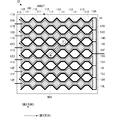
- FIG. 3 is a plan view of the first main surface 100ST of the main functional unit 10 configuring the touch panel 1 according to the first embodiment of the present invention.
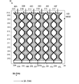
- FIG. 4 is a plan view of the second main surface 100SB of the main function unit 10 constituting the touch panel 1 according to the first embodiment of the present invention.
- 3 and 4 are views of the first main surface 100ST and the second main surface 100SB as viewed from the first main surface 100SST side. 1, 2, 3, and 4 are examples, and the first capacitance detection sub-electrode, the second capacitance detection sub-electrode, the first piezoelectric voltage detection sub-electrode, and The number of the second piezoelectric voltage detection sub-electrodes is not limited to this, and the number is appropriately determined according to the specifications of the touch panel.
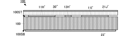
- the touch panel 1 includes a piezoelectric film 100, protective layers 30 and 40, a piezoelectric voltage detection electrode and a capacitance detection electrode formed in a pattern to be described later.
- the piezoelectric film 100 is formed of a rectangular flat film having a first main surface 100ST and a second main surface 100SB facing each other.
- the piezoelectric film 100 is made of uniaxially stretched L-type polylactic acid (PLLA).
- PLLA is a chiral polymer and its main chain has a helical structure.
- PLLA is uniaxially stretched and has piezoelectricity when the molecules are oriented.
- the piezoelectric constant of uniaxially stretched PLLA belongs to a very high class among the piezoelectric constants of various polymers.
- the draw ratio is preferably about 3 to 8 times.
- the same effect as that of uniaxial stretching can be obtained by varying the stretching ratio of each axis. For example, when a certain direction is taken as an X-axis, 8 times in that direction, and 2 times in the Y-axis direction perpendicular to that axis, the piezoelectric constant is about 4 times in the X-axis direction, The same effect can be obtained. Since a film that is simply uniaxially stretched easily tears along the direction of the stretch axis, the strength can be somewhat increased by performing biaxial stretching as described above.
- PLLA generates piezoelectricity by molecular orientation processing such as stretching, and there is no need to perform poling processing like other polymers such as PVDF and piezoelectric ceramics. That is, the piezoelectricity of PLLA that does not belong to ferroelectrics is not expressed by the polarization of ions like ferroelectrics such as PVDF and PZT, but is derived from a helical structure that is a characteristic structure of molecules. is there. For this reason, the pyroelectricity generated in other ferroelectric piezoelectric materials does not occur in PLLA. Further, PVDF or the like shows a change in piezoelectric constant over time, and in some cases, the piezoelectric constant may be significantly reduced, but the piezoelectric constant of PLLA is extremely stable over time.
- PLLA has a low dielectric constant, unlike a general ferroelectric that can obtain a high piezoelectric constant. Therefore, the electric field confinement effect between the electrode formed on first main surface 100ST and the electrode formed on second main surface 100SB is low. Thereby, if a dielectric such as a finger approaches or contacts from the outside, the capacitance is likely to change. That is, the detection sensitivity to the change in capacitance is high.
- the first main surface 100ST of the piezoelectric film 100 made of PLLA having such characteristics is provided with a plurality of first capacitance detection sub-electrodes 11A to 11F constituting capacitance detection electrodes and a piezoelectric voltage detection.
- a plurality of first piezoelectric voltage detection sub-electrodes 13A to 13L constituting the electrodes are formed in a pattern as shown in FIGS.
- the plurality of first capacitance detection sub-electrodes 11A to 11F and the plurality of first piezoelectric voltage detection sub-electrodes 13A to 13L are organic electrodes mainly composed of ITO, ZnO, polythiophene, and polyaniline as a main component.
- an organic electrode it is preferable to use any one of an organic electrode, an electrode using silver nanowires, and an electrode using carbon nanotubes.
- an electrode pattern with high translucency can be formed.
- These materials are formed by vapor deposition, sputtering, plating, or the like.
- a metal electrode other than the above-mentioned material formed by vapor deposition, sputtering, plating, or the like, or an electrode formed of silver paste can be used.
- the plurality of first capacitance detection sub-electrodes 11A to 11F have the same shape.
- the first capacitance detection sub-electrode 11A includes a plurality of wide portions 111, a plurality of narrow portions 112, and a pair of wide portions 113 for end portions.
- Each wide portion 111 is a square.
- the wide portion 111 does not necessarily have to be a square, and may be a rhombus, a parallelogram, or the like, and can have any shape required by the detection IC.
- the narrow portion 112 has a rectangular shape with a long length with respect to the width.
- the wide portion 113 for the end portion is formed of a substantially isosceles triangle.
- the plurality of wide portions 111 and the plurality of narrow portions 112 are connected so as to be alternately arranged along the extending direction of the first capacitance detection sub-electrode 11A. At this time, each wide portion 111 is connected to the narrow portion 112 so that the diagonal line of the square and the connection direction to the narrow portion 112 are parallel to each other. Further, each wide portion 111 is connected to the narrow portion 112 at a pair of apex angles forming the diagonal line.
- Wide ends 113 for end portions are provided at both ends in the extending direction of the first capacitance detection sub-electrode 11A. Both ends of the continuous electrode pattern composed of the plurality of wide portions 111 and the plurality of narrow portions 112 are connected to the wide portions 113 for the end portions by the narrow portions 112. At this time, the wide portion 113 for the end portion is connected to the narrow portion 112 at an apex angle of an isosceles triangle.
- the plurality of first capacitance detection sub-electrodes 11A to 11F are formed so as to extend along the first direction on the first main surface 100ST of the piezoelectric film 100.
- the plurality of first capacitance detection sub-electrodes 11A to 11F are formed at predetermined intervals along a second direction orthogonal to the first direction on the first main surface 100ST.
- the plurality of first capacitance detection sub-electrodes 11A to 11F are arranged so that the wide portions 111 are at the same position along the first direction, in other words, the wide portions 111 are respectively in the second direction. It is formed so that it may be arranged along.
- the first direction and the second direction are set to directions that form an angle of about 45 ° with respect to the uniaxial stretching direction 900 of the piezoelectric film 100.
- About 45 ° means an angle including about 45 ° ⁇ 10 °, for example.
- These angles are design items that should be determined as appropriate based on the overall design, such as bending detection accuracy, based on the application of the displacement sensor.
- the plurality of first piezoelectric voltage detection sub-electrodes 13A to 13L are shaped along the outer shape of the first capacitance detection sub-electrodes 11A to 11F, and are separated from the first capacitance detection sub-electrodes 11A to 11F. Is formed.
- the first piezoelectric voltage detection sub-electrode 13A is arranged along the outer diameter shape of the first capacitance detection sub-electrode 11A opposite to the first capacitance detection sub-electrode 11B.
- 1 Capacitance detection sub-electrode 11A is formed apart from it.
- the first piezoelectric voltage detection sub-electrode 13B is arranged along the outer diameter shape of the first capacitance detection sub-electrode 11A on the first capacitance detection sub-electrode 11B side. It is formed away from the electrode 11A.
- the first piezoelectric voltage detection sub-electrode 13C is arranged along the outer diameter shape of the first capacitance detection sub-electrode 11B on the first capacitance detection sub-electrode 11A side. It is formed away from the electrode 11B.
- the first piezoelectric voltage detection sub-electrodes 13B and 13C are connected to each other in the vicinity of the corners of the wide portion 111 and the wide end portion 113 of the first capacitance detection sub-electrode.
- the first piezoelectric voltage detection sub-electrode 13D is arranged along the outer diameter shape of the first capacitance detection sub-electrode 11B on the first capacitance detection sub-electrode 11C side. It is formed away from the electrode 11B.
- the first piezoelectric voltage detection sub-electrode 13E is arranged along the outer diameter shape of the first capacitance detection sub-electrode 11C on the first capacitance detection sub-electrode 11B side. It is formed away from the electrode 11C.
- the first piezoelectric voltage detection sub-electrodes 13D and 13E are connected to each other in the vicinity of the corners of the wide portion 111 and the wide end portion 113 of the first capacitance detection sub-electrode.
- the first piezoelectric voltage detection sub-electrode 13F is arranged along the outer diameter shape of the first capacitance detection sub-electrode 11C on the first capacitance detection sub-electrode 11D side. It is formed away from the electrode 11C.
- the first piezoelectric voltage detection sub-electrode 13G is arranged along the outer diameter shape of the first capacitance detection sub-electrode 11D on the first capacitance detection sub-electrode 11C side. It is formed apart from the electrode 11D.
- the first piezoelectric voltage detection sub-electrodes 13F and 13G are connected to each other in the vicinity of the corners of the wide portion 111 and the wide end portion 113 of the first capacitance detection sub-electrode.
- the first piezoelectric voltage detection sub-electrode 13H is arranged along the outer diameter shape of the first capacitance detection sub-electrode 11D on the first capacitance detection sub-electrode 11E side. It is formed apart from the electrode 11D.
- the first piezoelectric voltage detection sub-electrode 13I is arranged along the outer diameter shape of the first capacitance detection sub-electrode 11E on the first capacitance detection sub-electrode 11D side. It is formed apart from the electrode 11E.
- the first piezoelectric voltage detection sub-electrodes 13H and 13I are connected to each other in the vicinity of the corners of the wide portion 111 and the wide end portion 113 of the first capacitance detection sub-electrode.
- the first piezoelectric voltage detection sub-electrode 13J is arranged along the outer diameter shape of the first capacitance detection sub-electrode 11E on the first capacitance detection sub-electrode 11F side. It is formed apart from the electrode 11E.
- the first piezoelectric voltage detection sub-electrode 13K is arranged along the outer diameter shape of the first capacitance detection sub-electrode 11F on the first capacitance detection sub-electrode 11E side. It is formed away from the electrode 11F.
- the first piezoelectric voltage detection sub-electrodes 13J and 13K are connected to each other in the vicinity of the corners of the wide portion 111 and the wide end portion 113 of the first capacitance detection sub-electrode.
- the first piezoelectric voltage detection sub-electrode 13L is arranged along the outer diameter shape of the first capacitance detection sub-electrode 11F opposite to the first capacitance detection sub-electrode 11E. It is formed apart from the sub electrode 11F for use.
- the first piezoelectric voltage detection sub-electrodes 13A to 13K are grouped together by the routing electrode 14 and connected to an external circuit.
- the first capacitance detection sub-electrodes 11A to 11F are individually connected to the routing electrodes 12A to 12F, respectively, and connected to an external circuit via the routing electrodes 12A to 12F.
- the routing electrodes 12A to 12F and 14 are formed outside the region where the first capacitance detection sub-electrodes 11A to 11F and the first piezoelectric voltage detection sub-electrodes 13A to 13K are formed. Further, the routing electrodes 12A to 12F are formed at one end in the first direction, and the routing electrode 14 is formed at the other end in the first direction.
- a plurality of second capacitance detection sub-electrodes 21A, 21B, 21C, 21D, 21E, 21F constituting the capacitance detection electrode, and a piezoelectric voltage detection are in a pattern as shown in FIGS. Is formed.
- the plurality of second capacitance detection sub-electrodes 21A to 21F and second piezoelectric voltage detection sub-electrodes 23A to 23L are also organic electrodes mainly composed of ITO, ZnO, polythiophene, and organic electrodes mainly composed of polyaniline. It is preferable to use either an electrode using silver nanowires or an electrode using carbon nanotubes. By using these materials, an electrode pattern with high translucency can be formed. When transparency is not required, an electrode formed of silver paste, or a metal electrode formed by vapor deposition, sputtering, plating, or the like can be used.
- the plurality of second capacitance detection sub-electrodes 21A to 21F have the same shape.
- the second capacitance detection sub-electrode 21A includes a plurality of wide portions 211, a plurality of narrow portions 212, and a pair of wide portions 213 for end portions.
- Each wide portion 211 is a square.
- the wide portion 211 is not necessarily square, and may be a rhombus, a parallelogram, or the like, and can have any shape required by the detection IC.
- the narrow portion 212 has a rectangular shape with a long length with respect to the width.
- the wide portion 213 for the end portion is formed of a substantially isosceles triangle.
- the plurality of wide portions 211 and the plurality of narrow portions 212 are connected to be alternately arranged along the extending direction of the second capacitance detection sub-electrode 21A. At this time, each wide portion 211 is connected to the narrow portion 212 so that the diagonal line of the square and the connection direction to the narrow portion 212 are parallel to each other. Further, each wide portion 211 is connected to the narrow portion 212 at a pair of apex angles forming the diagonal line.
- Wide ends 213 for end portions are provided at both ends in the extending direction of the second capacitance detection sub-electrode 21A. Both ends of a continuous electrode pattern composed of a plurality of wide portions 211 and a plurality of narrow portions 212 are connected to the wide portions 213 for the end portions by the narrow portions 212. At this time, the wide portion 213 for the end portion is connected to the narrow portion 212 at an apex angle of an isosceles triangle.
- the plurality of second capacitance detection sub-electrodes 21A to 21F are formed to extend along the second direction of the second main surface 100SB of the piezoelectric film 100.
- the plurality of second capacitance detection sub-electrodes 21A to 21F are formed at predetermined intervals along a first direction orthogonal to the second direction on the second main surface 100SB.
- the plurality of second capacitance detection sub-electrodes 21A to 21F are arranged so that the wide portions 211 are at the same position along the second direction, in other words, the wide portions 211 are respectively in the first direction. It is formed so that it may be arranged along.
- the plurality of second capacitance detection sub-electrodes 21A to 21F are configured such that the wide portions 212 do not face the wide portions 111 of the first capacitance detection sub-electrodes 11A to 11F via the piezoelectric film 100. Is formed.
- the wide portions 212 constituting the plurality of second capacitance detection sub-electrodes 21A to 21F constitute the first capacitance detection sub-electrodes 11A to 11F.
- the second capacitance detection sub-electrodes 21A to 21F are formed so as not to overlap the wide portions 111 to be performed.
- the plurality of first capacitance detection sub-electrodes 11A to 11F and the plurality of second capacitance detection sub-electrodes 21A to 21F are piezoelectric only at the narrow portions 112 and 212. It faces through the film 100.
- the wide portions 211 constituting the plurality of second capacitance detection sub-electrodes 21A to 21F and the first capacitance detection sub-electrodes 11A to 11F are constituted.
- the first capacitance detection sub-electrodes 11A to 11F and the second capacitance detection sub-electrodes 21A to 21F are formed so that gaps with a predetermined width are formed between the wide portions 111.
- the width of the gap is set so that the first piezoelectric voltage detection sub-electrodes 13A to 13K formed on the first main surface 100ST are within the gap when viewed from the first main surface 100ST side. ing.
- the plurality of second piezoelectric voltage detection sub-electrodes 23A to 23L are shaped along the outer diameter of the second capacitance detection sub-electrodes 21A to 21F, and are connected to the second capacitance detection sub-electrodes 21A to 21F. They are spaced apart.
- the second piezoelectric voltage detection sub-electrode 23A is arranged along the outer diameter shape of the second capacitance detection sub-electrode 21A opposite to the second capacitance detection sub-electrode 21B. 2 It is formed apart from the capacitance detecting sub-electrode 21A.
- the second piezoelectric voltage detection sub-electrode 23B is arranged along the outer diameter shape of the second capacitance detection sub-electrode 21A on the second capacitance detection sub-electrode 21B side. It is formed away from the electrode 21A.
- the second piezoelectric voltage detection sub-electrode 23C extends along the outer diameter shape of the second capacitance detection sub-electrode 21B on the second capacitance detection sub-electrode 21A side. It is formed away from the electrode 21B.
- the second piezoelectric voltage detection sub-electrodes 23B and 23C are connected to each other in the vicinity of the corners of the wide portion 211 and the wide end portion 213 of the second capacitance detection sub-electrode.
- the second piezoelectric voltage detection sub-electrode 23D is arranged along the outer diameter shape of the second capacitance detection sub-electrode 21B on the second capacitance detection sub-electrode 21C side. It is formed away from the electrode 21B.
- the second piezoelectric voltage detection sub-electrode 23E is arranged along the outer diameter shape of the second capacitance detection sub-electrode 21C on the second capacitance detection sub-electrode 21B side. It is formed away from the electrode 21C.
- the second piezoelectric voltage detection sub-electrodes 23D and 23E are connected to each other in the vicinity of the corners of the wide portion 211 and the wide end portion 213 of the second capacitance detection sub-electrode.
- the second piezoelectric voltage detection sub-electrode 23F is arranged along the outer diameter shape of the second capacitance detection sub-electrode 21C on the second capacitance detection sub-electrode 21D side. It is formed away from the electrode 21C.
- the second piezoelectric voltage detection sub-electrode 23G is arranged along the outer diameter shape of the second capacitance detection sub-electrode 21D on the second capacitance detection sub-electrode 21C side. It is formed away from the electrode 21D.
- the second piezoelectric voltage detection sub-electrodes 23F and 23G are connected to each other in the vicinity of the corners of the wide portion 211 and the wide end portion 213 of the second capacitance detection sub-electrode.
- the second piezoelectric voltage detection sub-electrode 23H extends along the outer diameter shape of the second capacitance detection sub-electrode 21D on the second capacitance detection sub-electrode 21E side. It is formed away from the electrode 21D.
- the second piezoelectric voltage detection sub-electrode 23I is arranged along the outer diameter shape of the second capacitance detection sub-electrode 21E on the second capacitance detection sub-electrode 21D side. It is formed away from the electrode 21E.
- the second piezoelectric voltage detection sub-electrodes 23H and 23I are connected to each other in the vicinity of the corners of the wide portion 211 and the wide end portion 213 of the second capacitance detection sub-electrode.
- the second piezoelectric voltage detection sub-electrode 23J is arranged along the outer diameter shape of the second capacitance detection sub-electrode 21E on the second capacitance detection sub-electrode 21F side. It is formed away from the electrode 21E.
- the second piezoelectric voltage detection sub-electrode 23K is arranged along the outer diameter shape of the second capacitance detection sub-electrode 21F on the second capacitance detection sub-electrode 21E side. It is formed away from the electrode 21F.
- the second piezoelectric voltage detection sub-electrodes 23J and 23K are connected to each other in the vicinity of the corners of the wide portion 211 and the wide end portion 213 of the second capacitance detection sub-electrode.
- the second piezoelectric voltage detection sub-electrode 23L is arranged along the outer diameter shape of the second capacitance detection sub-electrode 21F opposite to the second capacitance detection sub-electrode 21E. It is formed apart from the sub electrode 21F for use.
- the second piezoelectric voltage detection sub-electrodes 23A to 23L formed on the second main surface 100SB and the first piezoelectric voltage detection sub-electrodes 13A to 13K formed on the first main surface 100ST are wide portions 211 and 213, respectively. Are formed so as to face each other through the piezoelectric film 100 over substantially the entire length in a gap seen from the first main surface 100ST side generated between the wide film portions 111 and 113.
- the second piezoelectric voltage detection sub-electrode 23A includes a wide portion 213 for the end of the second capacitance detection sub-electrode 21A and a first capacitance detection sub-electrode 11A.
- the first piezoelectric voltage detection sub-electrode 13A is opposed to the wide end portion 113 for the end portion.
- the second piezoelectric voltage detection sub-electrode 23A includes a wide portion 211 of the second capacitance detection sub-electrode 21A and a wide portion 113 for the ends of the first capacitance detection sub-electrodes 11A and 11B.
- the first piezoelectric voltage detection sub-electrodes 13B and 13C are opposed to each other.
- the other portions of the second piezoelectric voltage detection sub-electrode 23A are similarly opposed to the first piezoelectric voltage detection sub-electrodes 13D to 13L, and the other second piezoelectric voltage detection sub-electrodes 23A to 13L.
- the electrodes 23B to 23L also face the first piezoelectric voltage detection sub-electrodes 13A to 13L, respectively.
- the second piezoelectric voltage detection sub-electrodes 23A to 23K are grouped together by the routing electrode 24 and connected to an external circuit.
- the second capacitance detection sub-electrodes 21A to 21F are individually connected to the routing electrodes 22A to 22F, and are connected to an external circuit via the routing electrodes 22A to 22F.
- the routing electrodes 22A to 22F and 24 are formed outside the formation area of the second capacitance detection sub-electrodes 21A to 21F and the second piezoelectric voltage detection sub-electrodes 23A to 23K. Further, the routing electrodes 22A to 22F are formed at one end in the second direction, and the routing electrode 24 is formed at the other end in the second direction.
- the main functional unit 10 of the touch panel 1 is configured by the piezoelectric film 100 on which ⁇ 23L is formed.
- the protective layer 30 is disposed so as to cover.
- the protective layer 30 has an insulating property and is formed of a light-transmitting material. Note that in the case where translucency is not required, the material is not particularly limited as long as it has insulating properties.
- the entire electrode pattern formation region of the second capacitance detection sub-electrodes 21A to 21F and the second piezoelectric voltage detection sub-electrodes 23A to 23L is formed.
- a protective layer 40 is disposed so as to cover.
- the protective layer 40 is also made of a material having insulating properties and translucency. Note that in the case where translucency is not required, the material is not particularly limited as long as it has insulating properties.
- the protective layers 30 and 40 may be made of polyethylene terephthalate PET, polyethylene naphthalate PEN, polypropylene PP, or the like, and may be formed in a shape (thickness or the like) that does not inhibit the bending of the piezoelectric film 100.
- the touch panel 1 having the above structure detects the touch position and the push-in amount as shown below.
- the routing electrodes 12A to 12F and 22A to 22F for detecting the capacitance are connected to the capacitance detecting circuit.
- the lead electrodes 14 and 24 for detecting the piezoelectric voltage are connected to a piezoelectric voltage detecting circuit.
- the touch position is detected by the following principle.
- a so-called projection type mutual capacitance method touch position detection concept is used, and a detailed description of the detection concept is omitted. Therefore, the touch position detection concept will be schematically described below.
- a drive signal is applied between the first capacitance detection sub-electrodes 11A to 11F and the second capacitance detection sub-electrodes 21A to 21F via the routing electrodes 12A to 12F and the routing electrodes 22A to 22F. Is done.
- the first capacitance detection sub-electrodes 11A to 11F extend in the first direction and are arranged at predetermined intervals along the second direction. Since 21A to 21F extend in the second direction and are arranged at predetermined intervals along the first direction, the first capacitance detection sub-electrodes 11A to 11F and the second capacitance detection sub-electrode The positions at which 21A to 21F face each other through the piezoelectric film 100, in other words, the positions at which an electric field is generated and a detection current flows, are the first capacitance detection sub-electrode and the second capacitance that constitute the facing position. Two-dimensional coordinates can be detected from the combination with the detection sub-electrode.
- the touch position can be detected.
- first capacitance detection sub-electrodes 11A to 11F and the second capacitance detection sub-electrodes 21A to 21F of the present embodiment are viewed along a direction orthogonal to the first main surface 100ST which is an operation surface.
- first capacitance detection sub-electrodes 11A to 11F and the second capacitance detection are arranged so as to face each other at the narrow portions 112 and 212 and not to overlap each other at the wide portions 111 and 112. Electric field changes due to the touch of the finger are likely to occur on both the sub electrodes 21A to 21F. Thereby, the detection sensitivity of a touch can be improved.
- the piezoelectric film 100 is PLLA, the dielectric constant for forming the capacitance is low, and it is easily affected by the outside. Thereby, an electric field change due to a finger touch is more likely to occur, and the touch detection sensitivity can be further improved.
- FIG. 5 is a diagram for explaining the push-in amount detection function of the main function unit 10 according to the first embodiment of the present invention.
- FIG. 5A shows a state where the pushing force is not involved
- FIG. 5B shows a state where the pushing force by the finger is concerned.
- FIG. 6A is a graph showing the correlation between the push-in amount and the detection voltage
- FIG. 6B is a waveform diagram of the push-in detection voltage of the main function unit 10 according to the first embodiment of the present invention. It is.
- the main functional unit 10 of the touch panel 1 is attached to one main surface of the flat elastic body 50 so that the flat surfaces are in close contact with each other.
- the elastic body 50 is made of glass, acrylic, polycarbonate, or the like.
- the elastic body 50 is not limited to the material described here, and an appropriate material may be selected according to the use conditions. Moreover, what is necessary is just to select an appropriate surface according to use conditions also about the surface which bonds the main function part 10 of the touch panel 1.
- the opposite ends of the elastic body 50 are supported by the support body 501. That is, in the case of the touch panel 1, both ends in the first direction of the touch panel 1 are fixed. In this state, since the elastic body 50 is not bent and no stress is applied to the piezoelectric film 100, no charge is generated.
- the elastic body 50 when the surface of the elastic body 50 is pressed with a finger 510, a pressing force as shown by a thick arrow 520 is applied to the elastic body 50.
- the elastic body 50 is curved so as to swell toward the arrangement surface side of the main function unit 10.
- the piezoelectric film 100 of the main functional unit 10 is stretched substantially along the first direction, and a tensile stress as indicated by a thick arrow 530 is generated. Due to this stress, the piezoelectric film 100 is polarized into the first main surface 100ST and the second main surface 100SB.
- the first piezoelectric voltage detection sub-electrodes 13A to 13L are formed on the first main surface 100ST, and the second piezoelectric voltage detection sub-electrodes 23A to 23L are formed on the second main surface 100SB.
- a potential difference is generated between the first piezoelectric voltage detection sub-electrodes 13A to 13L and the second piezoelectric voltage detection sub-electrodes 23A to 23L. Therefore, by detecting this potential difference, that is, the piezoelectric voltage, it is possible to detect pressing by a finger, in other words, pressing by a finger touch.
- the detection voltage (piezoelectric voltage) changes linearly as the film is stretched according to the amount of pressing. Therefore, the push-in amount can be detected by measuring the detection voltage value with the piezoelectric voltage detection circuit. That is, it is possible to accurately detect whether the operator has touched the operation surface lightly or pressed it strongly.
- the detection voltage by the piezoelectric film 100 is normally generated at the moment when the stress is generated, and the detection voltage value is rapidly decreased with the leakage of electric charge due to the piezoelectric effect.
- the detection voltage value can be maintained for a predetermined time as shown in FIG. 6B. As a result, the detected voltage value can be more reliably measured and the push-in amount can be detected. Similar effects can be obtained by integrating signals in a software manner instead of the detection circuit and the integration circuit having a large input impedance.
- the touch position and the push-in amount can be obtained simply by forming the capacitance detection electrode and the piezoelectric voltage detection electrode on both opposing surfaces of one piezoelectric film 100. Pressure) can be detected simultaneously. Furthermore, a touch panel with high translucency can be realized.
- PLLA is a polymer and has flexibility, so that it is not damaged by a large displacement unlike piezoelectric ceramics. Therefore, even if the displacement amount is large, the displacement amount can be reliably detected.
- the protective layers 30 and 40 are simply disposed.
- the elastic body 50 such as an acrylic plate having a high elastic modulus is provided on the first main surface 100ST side of the main functional unit 10.
- the protective layer 40 may be disposed only on the second main surface 100SB side.
- the protective layers 30 and 40 may be provided so that the surface of the protective layer 40 on the side opposite to the main functional portion 10 has adhesiveness. Furthermore, by making this adhesiveness weakly adhesive, it is possible to realize a touch panel that can be mounted or removed depending on the place of use.
- FIG. 7 is a diagram for explaining a first manufacturing method of the touch panel 1.
- FIG. 8 is a diagram for explaining a second manufacturing method of the touch panel 1. In FIG. 7 and FIG. 8, detailed electrode patterns are not shown, but are simply shown.
- the first capacitance detection sub-electrodes 11A to 11F, the first piezoelectric voltage detection sub-electrodes 13A to 13L, and the routing electrode are formed on the first main surface 100ST of the piezoelectric film 100.
- 12A to 12F and 14 are formed.
- the second capacitance detection sub-electrodes 21A to 21F, the second piezoelectric voltage detection sub-electrodes 23A to 23L, and the routing electrodes 22A to 22F and 24 are formed on the second main surface 100SB of the piezoelectric film 100. .
- the order of electrode formation on the first main surface 100ST and the second main surface 100SB may be reversed. Thereby, the main function unit 10 is configured first.
- the protective layer 30 is disposed on the first main surface 100ST side of the piezoelectric film 100 in the main function unit 10. And the protective layer 40 is arrange
- the first capacitance detection sub-electrodes 11A to 11F, the first piezoelectric voltage detection sub-electrodes 13A to 13L, and the routing electrodes 12A to 12F are formed on one main surface of the protective layer 30. , 14 are formed.
- the second capacitance detection sub-electrodes 21A to 21F, the second piezoelectric voltage detection sub-electrodes 23A to 23L, and the routing electrodes 22A to 22F, 24 are formed on one main surface of the protective layer 40.
- the protective layer 30 on which the electrode pattern is formed is adhered to the first main surface 100ST of the piezoelectric film 100 so that the electrode pattern surface is on the piezoelectric film 100 side. Further, the protective layer 40 on which the electrode pattern is formed is adhered to the second main surface 100SB of the piezoelectric film 100 so that the electrode pattern surface is on the piezoelectric film 100 side. Thereby, the touch panel 1 is formed.
- a touch panel can be formed by an easy process as compared with the manufacturing method of FIG. This is because the surface of the PLLA is inactive, and thus when the electrode pattern is formed, a process for improving the adhesion of the electrode is required.
- the protective layers 30 and 40 are formed of PET or PEN, electrode formation is easy. Therefore, the touch panel 1 can be easily manufactured by using the manufacturing method of FIG.
- any treatment is performed on the surface of PLLA, the light transmittance of PLLA may be lowered. Therefore, if the use application places importance on light transmittance, it is better to use the manufacturing method of FIG. .
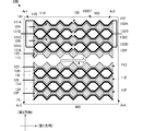
- FIG. 9 is a plan view of the first main surface 100ST of the main functional unit 10A constituting the touch panel 1A according to the second embodiment of the present invention.
- FIG. 10 is a plan view of the second main surface 100SB of the main functional unit 10A constituting the touch panel 1A according to the second embodiment of the present invention.
- the touch panel 1A of the present embodiment is different from the touch panel 1 shown in the first embodiment only in the fixing structure, the uniaxial stretching direction of the piezoelectric film 100, and the shape of the piezoelectric voltage detection sub-electrode, Other configurations are the same. Therefore, below, only a different part from the touch panel 1 shown in 1st Embodiment is demonstrated concretely.
- the touch panel 1A of the present embodiment has a structure in which the four sides of the piezoelectric film 100 are fixed. At this time, the piezoelectric film 100 is formed such that the uniaxial stretching direction 900 is orthogonal to the pair of fixed sides and parallel to the other pair of fixed sides.
- first capacitance detection sub-electrodes 11A to 11F are formed on the first main surface 100ST of the piezoelectric film 100. As shown in FIG. The first capacitance detection sub-electrodes 11A to 11F have the same structure as that of the first embodiment, but the extending direction of the first capacitance detection sub-electrodes 11A to 11F is a uniaxial extension direction 900 (first direction). ) To be parallel to each other.
- the first piezoelectric voltage detection sub-electrodes 131A and 132A are arranged along the outer diameter of the first capacitance detection sub-electrode 11A opposite to the first capacitance detection sub-electrode 11B. It is formed apart from the capacitance detection sub-electrode 11A.
- the first piezoelectric voltage detection sub-electrodes 131A and 132A are separated at an intermediate point along the first direction, and one end side along the first direction from the separation point 150 becomes the first piezoelectric voltage detection sub-electrode 131A.
- the other end side along the first direction from the separation point 150 is the first piezoelectric voltage detection sub-electrode 132A.
- the first piezoelectric voltage detection sub-electrodes 131B and 132B are arranged along the outer diameter shape on the first capacitance detection sub-electrode 11B side in the first capacitance detection sub-electrode 11A. It is formed apart from the sub electrode 11A for use.
- the first piezoelectric voltage detection sub-electrodes 131B and 132B are separated at an intermediate point along the first direction, and one end side along the first direction from the separation point 150 becomes the first piezoelectric voltage detection sub-electrode 131B.
- the other end side along the first direction from the separation point 150 is the first piezoelectric voltage detection sub-electrode 132B.
- the first piezoelectric voltage detection sub-electrodes 131C and 132C are arranged along the outer diameter shape of the first capacitance detection sub-electrode 11B on the first capacitance detection sub-electrode 11A side. It is formed away from the sub electrode 11B for use.
- the first piezoelectric voltage detection sub-electrodes 131C and 132C are separated at an intermediate point along the first direction, and one end side along the first direction from the separation point 150 becomes the first piezoelectric voltage detection sub-electrode 131C.
- the other end along the first direction from the separation point 150 is the first piezoelectric voltage detecting sub-electrode 132C.
- the first piezoelectric voltage detection sub-electrodes 131B and 131C are connected to each other in the vicinity of the corners of the wide portion 111 and the wide end portion 113 of the first capacitance detection sub-electrode.
- the first piezoelectric voltage detection sub-electrodes 132B and 132C are connected to each other in the vicinity of the corners of the wide portion 111 and the wide end portion 113 of the first capacitance detection sub-electrode.
- the first piezoelectric voltage detection sub-electrodes 131D and 132D are arranged along the outer diameter shape of the first capacitance detection sub-electrode 11B on the first capacitance detection sub-electrode 11C side. It is formed away from the sub electrode 11B for use.
- the first piezoelectric voltage detection sub-electrodes 131D and 132D are separated at an intermediate point along the first direction, and one end side along the first direction from the separation point 150 is the first piezoelectric voltage detection sub-electrode 131D.
- the other end side along the first direction from the separation point 150 is the first piezoelectric voltage detection sub-electrode 132D.
- the first piezoelectric voltage detection sub-electrodes 131E and 132E are arranged along the outer diameter shape of the first capacitance detection sub-electrode 11C on the first capacitance detection sub-electrode 11B side. It is formed away from the sub electrode 11C.
- the first piezoelectric voltage detection sub-electrodes 131E and 132E are separated at an intermediate point along the first direction, and one end side along the first direction from the separation point 150 becomes the first piezoelectric voltage detection sub-electrode 131E.
- the other end side in the first direction from the separation point 150 is the first piezoelectric voltage detection sub-electrode 132E.
- the first piezoelectric voltage detection sub-electrodes 131D and 131E are connected to each other in the vicinity of the corners of the wide portion 111 and the wide end portion 113 of the first capacitance detection sub-electrode.
- the first piezoelectric voltage detection sub-electrodes 132D and 132E are connected to each other in the vicinity of the corners of the wide portion 111 and the wide end portion 113 of the first capacitance detection sub-electrode.
- the first piezoelectric voltage detection sub-electrodes 131A, 131B, 131C, 131D, and 131E are grouped together by the lead-out electrode 141, and are connected to an external circuit from one end side in the first direction of the piezoelectric film 100.
- the first piezoelectric voltage detection sub-electrodes 132A, 132B, 132C, 132D, and 132E are grouped together by the lead-out electrode 142, and are connected to the external circuit from the other end side in the first direction of the piezoelectric film 100.
- a piezoelectric voltage detection subelectrode is provided between the first capacitance detection subelectrode 11C and the first capacitance detection subelectrode 11D, which is a central region along the second direction of the first main surface 100ST. Not formed.
- the first piezoelectric voltage detection sub-electrodes 131H and 132H are arranged along the outer diameter shape of the first capacitance detection sub-electrode 11D on the first capacitance detection sub-electrode 11E side. It is formed away from the sub electrode 11D for use.
- the first piezoelectric voltage detection sub-electrodes 131H and 132H are separated at an intermediate point along the first direction, and one end side along the first direction from the separation point 150 becomes the first piezoelectric voltage detection sub-electrode 131H.
- the other end side along the first direction from the separation point 150 is the first piezoelectric voltage detection sub-electrode 132H.
- the first piezoelectric voltage detection sub-electrodes 131I and 132I are arranged along the outer diameter shape of the first capacitance detection sub-electrode 11E on the first capacitance detection sub-electrode 11D side. It is formed apart from the sub electrode 11E for use.
- the first piezoelectric voltage detection sub-electrodes 131I and 132I are separated at an intermediate point along the first direction, and one end side along the first direction from the separation point 150 becomes the first piezoelectric voltage detection sub-electrode 131I.
- the other end side along the first direction from the separation point 150 is the first piezoelectric voltage detection sub-electrode 132I.
- the first piezoelectric voltage detection sub-electrodes 131H and 131I are connected to each other in the vicinity of the corners of the wide portion 111 and the wide end portion 113 of the first capacitance detection sub-electrode.
- the first piezoelectric voltage detection sub-electrodes 132H and 132I are connected to each other in the vicinity of the corners of the wide portion 111 and the wide end portion 113 of the first capacitance detection sub-electrode.
- the first piezoelectric voltage detection sub-electrodes 131J and 132J are arranged along the outer diameter shape of the first capacitance detection sub-electrode 11E on the first capacitance detection sub-electrode 11F side. It is formed apart from the sub electrode 11E for use.
- the first piezoelectric voltage detection sub-electrodes 131J and 132J are separated at an intermediate point along the first direction, and one end side along the first direction from the separation point 150 becomes the first piezoelectric voltage detection sub-electrode 131J.
- the other end side along the first direction from the separation point 150 is the first piezoelectric voltage detection sub-electrode 132J.
- the first piezoelectric voltage detection sub-electrodes 131K and 132K are arranged along the outer diameter shape of the first capacitance detection sub-electrode 11F on the first capacitance detection sub-electrode 11E side. It is formed apart from the sub electrode 11F for use.
- the first piezoelectric voltage detection sub-electrodes 131K and 132K are separated at an intermediate point along the first direction, and one end side along the first direction from the separation point 150 becomes the first piezoelectric voltage detection sub-electrode 131K.
- the other end side along the first direction from the separation point 150 is the first piezoelectric voltage detection sub-electrode 132K.
- the first piezoelectric voltage detection sub-electrodes 131J and 131K are connected to each other in the vicinity of the corners of the wide portion 111 and the wide end portion 113 of the first capacitance detection sub-electrode.
- the first piezoelectric voltage detection sub-electrodes 132J and 132K are connected to each other in the vicinity of the corners of the wide portion 111 and the wide end portion 113 of the first capacitance detection sub-electrode.
- the first piezoelectric voltage detection sub-electrodes 131L and 132L are arranged along the outer diameter of the first capacitance detection sub-electrode 11F on the opposite side of the first capacitance detection sub-electrode 11E. It is formed away from the capacitance detection sub-electrode 11F.
- the first piezoelectric voltage detection sub-electrodes 131L and 132L are separated at an intermediate point along the first direction, and one end side along the first direction from the separation point 150 becomes the first piezoelectric voltage detection sub-electrode 131L.
- the other end side along the first direction from the separation point 150 is the first piezoelectric voltage detection sub-electrode 132L.
- the first piezoelectric voltage detection sub-electrodes 131H, 131I, 131J, 131K, and 131L are gathered together by a lead-out electrode 143, and are connected to an external circuit from one end side in the first direction of the piezoelectric film 100.
- the first piezoelectric voltage detection sub-electrodes 132H, 132I, 132J, 132K, and 132L are grouped together by the lead-out electrode 144, and are connected to the external circuit from the other end side in the first direction of the piezoelectric film 100.
- second capacitance detection sub-electrodes 21A to 21F are formed on the second main surface 100SB of the piezoelectric film 100, as shown in FIG. 10, second capacitance detection sub-electrodes 21A to 21F are formed.
- the second capacitance detection sub-electrodes 21A to 21F have the same structure as that of the first embodiment, but the extending direction of the second capacitance detection sub-electrodes 21A to 21F is orthogonal to the uniaxial extension direction 900. To be formed.
- the second piezoelectric voltage detection sub-electrodes 231A and 232A are arranged along the outer diameter of the second capacitance detection sub-electrode 21A on the opposite side of the second capacitance detection sub-electrode 21B. It is formed apart from the capacitance detection sub-electrode 21A.
- the second piezoelectric voltage detection sub-electrodes 231A and 232A are separated at an intermediate point along the second direction, and one end side along the second direction from the separation point 150 becomes the second piezoelectric voltage detection sub-electrode 231A.
- the other end side along the second direction from the separation point 150 is the second piezoelectric voltage detection sub-electrode 232A.
- the second piezoelectric voltage detection sub-electrodes 231B and 232B detect the second capacitance detection along the outer diameter shape of the second capacitance detection sub-electrode 21B on the second capacitance detection sub-electrode 21B side. It is formed away from the sub electrode 21A for use.
- the second piezoelectric voltage detection sub-electrodes 231B and 232B are separated at an intermediate point along the second direction, and one end side along the second direction from the separation point 150 becomes the second piezoelectric voltage detection sub-electrode 231B.
- the other end side along the second direction from the separation point 150 is the second piezoelectric voltage detection sub-electrode 232B.
- the second piezoelectric voltage detection sub-electrodes 231C and 232C detect the second capacitance detection along the outer diameter shape of the second capacitance detection sub-electrode 21B on the second capacitance detection sub-electrode 21A side. It is formed away from the sub electrode 21B.
- the second piezoelectric voltage detection sub-electrodes 231C and 232C are separated at an intermediate point along the second direction, and one end side along the second direction from the separation point 150 becomes the second piezoelectric voltage detection sub-electrode 231C.
- the other end side along the second direction from the separation point 150 is the second piezoelectric voltage detection sub-electrode 232C.
- the second piezoelectric voltage detection sub-electrodes 231B and 231C are connected to each other in the vicinity of the corners of the wide portion 211 and the wide end portion 213 of the second capacitance detection sub-electrode.
- the second piezoelectric voltage detection sub-electrodes 232B and 232C are connected to each other in the vicinity of the corners of the wide portion 211 and the wide end portion 213 of the second capacitance detection sub-electrode.
- the second piezoelectric voltage detection sub-electrodes 231D and 232D detect the second capacitance detection along the outer diameter shape of the second capacitance detection sub-electrode 21B on the second capacitance detection sub-electrode 21C side. It is formed away from the sub electrode 21B.
- the second piezoelectric voltage detection sub-electrodes 231D and 232D are separated at an intermediate point along the second direction, and one end side along the second direction from the separation point 150 is the second piezoelectric voltage detection sub-electrode 231D. The other end side along the second direction from the separation point 150 is the second piezoelectric voltage detection sub-electrode 232D.
- the second piezoelectric voltage detection sub-electrodes 231E and 232E detect the second capacitance detection along the outer diameter shape of the second capacitance detection sub-electrode 21B on the second capacitance detection sub-electrode 21B side. It is formed apart from the sub electrode 21C for use.
- the second piezoelectric voltage detection sub-electrodes 231E and 232E are separated at an intermediate point along the second direction, and one end side along the second direction from the separation point 150 becomes the second piezoelectric voltage detection sub-electrode 231E.
- the other end side along the second direction from the separation point 150 is the second piezoelectric voltage detection sub-electrode 232E.
- the second piezoelectric voltage detection sub-electrodes 231D and 231E are connected to each other in the vicinity of the corners of the wide portion 211 and the wide end portion 213 of the second capacitance detection sub-electrode.
- the second piezoelectric voltage detection sub-electrodes 232D and 232E are connected to each other in the vicinity of the corners of the wide portion 211 and the wide end portion 213 of the second capacitance detection sub-electrode.
- the second piezoelectric voltage detection sub-electrodes 231A, 231B, 231C, 231D, and 231E are gathered together by the lead-out electrode 241 and connected to an external circuit from one end side in the second direction of the piezoelectric film 100.
- the second piezoelectric voltage detection sub-electrodes 232A, 232B, 232C, 232D, and 232E are gathered together by the lead-out electrode 242, and are connected to the external circuit from the other end side of the piezoelectric film 100 in the second direction.
- the second piezoelectric voltage detection sub-electrodes 231H and 232H detect the second capacitance detection along the outer diameter shape of the second capacitance detection sub-electrode 21D on the second capacitance detection sub-electrode 21E side. It is formed apart from the sub electrode 21D for use.
- the second piezoelectric voltage detection sub-electrodes 231H and 232H are separated at an intermediate point along the second direction, and one end side along the second direction from the separation point 150 becomes the second piezoelectric voltage detection sub-electrode 231H.
- the other end side in the second direction from the separation point 150 is the second piezoelectric voltage detection sub-electrode 232H.
- the second piezoelectric voltage detection sub-electrodes 231I and 232I detect the second capacitance detection along the outer diameter shape of the second capacitance detection sub-electrode 21E on the second capacitance detection sub-electrode 21D side. It is formed apart from the sub electrode 21E for use.
- the second piezoelectric voltage detection sub-electrodes 231I and 232I are separated at an intermediate point along the second direction, and one end side along the second direction from the separation point 150 becomes the second piezoelectric voltage detection sub-electrode 231I.
- the other end side along the second direction from the separation point 150 is the second piezoelectric voltage detection sub-electrode 232I.
- the second piezoelectric voltage detection sub-electrodes 231H and 231I are connected to each other in the vicinity of the corners of the wide portion 211 and the wide end portion 213 of the second capacitance detection sub-electrode.
- the second piezoelectric voltage detection sub-electrodes 232H and 232I are connected to each other in the vicinity of the corners of the wide portion 211 and the wide end portion 213 of the second capacitance detection sub-electrode.
- the second piezoelectric voltage detection sub-electrodes 231J and 232J detect the second capacitance detection along the outer diameter shape of the second capacitance detection sub-electrode 21E on the second capacitance detection sub-electrode 21F side. It is formed apart from the sub electrode 21E for use.
- the second piezoelectric voltage detection sub-electrodes 231J and 232J are separated at an intermediate point along the second direction, and one end side along the second direction from the separation point 150 is the second piezoelectric voltage detection sub-electrode 231J. The other end side along the second direction from the separation point 150 is the second piezoelectric voltage detection sub-electrode 232J.
- the second piezoelectric voltage detection sub-electrodes 231K and 232K detect the second capacitance detection along the outer diameter shape of the second capacitance detection sub-electrode 21F on the second capacitance detection sub-electrode 21E side. It is formed apart from the sub electrode 21F for use.
- the second piezoelectric voltage detection sub-electrodes 231K and 232K are separated at an intermediate point along the second direction, and one end side along the second direction from the separation point 150 becomes the second piezoelectric voltage detection sub-electrode 231K.
- the other end side along the second direction from the separation point 150 is the second piezoelectric voltage detection sub-electrode 232K.
- the second piezoelectric voltage detection sub-electrodes 231J and 231K are connected to each other in the vicinity of the corners of the wide portion 211 and the wide end portion 213 of the second capacitance detection sub-electrode.
- the second piezoelectric voltage detection sub-electrodes 232J and 232K are connected to each other in the vicinity of the corners of the wide portion 211 and the wide end portion 213 of the second capacitance detection sub-electrode.
- the second piezoelectric voltage detection sub-electrodes 231L and 232L are arranged along the outer diameter of the second capacitance detection sub-electrode 21F on the opposite side of the second capacitance detection sub-electrode 21E. It is formed away from the capacitance detection sub-electrode 21F.
- the second piezoelectric voltage detection sub-electrodes 231L and 232L are separated at an intermediate point along the second direction, and one end side along the first direction from the separation point 150 becomes the second piezoelectric voltage detection sub-electrode 231L.
- the other end side along the first direction from the separation point 150 is the second piezoelectric voltage detection sub-electrode 232L.
- the second piezoelectric voltage detection sub-electrodes 231H, 231I, 231J, 231K, and 231L are gathered together by a lead-out electrode 243, and are connected to an external circuit from one end side in the second direction of the piezoelectric film 100.
- the second piezoelectric voltage detection sub-electrodes 232H, 232I, 232J, 232K, and 232L are gathered together by the lead-out electrode 244, and are connected to the external circuit from the other end side in the second direction of the piezoelectric film 100.
- Ar1, Ar2, Ar3, Ar4 can be detected individually.
- the piezoelectric voltage in the first partial region Ar1 is the first piezoelectric voltage detecting sub-electrode 131A, 131B, 131C, 131D, 131E on the first main surface 100ST and the second piezoelectric voltage detecting sub-electrode 231A on the second main surface 100SB. , 231B, 231C, 231D, and 231E.
- the piezoelectric voltage in the second partial area Ar2 is the first piezoelectric voltage detecting sub-electrodes 132A, 132B, 132C, 132D, 132E on the first main surface 100ST and the second piezoelectric voltage detecting sub-electrode 231H on the second main surface 100SB. , 231I, 231J, 231K, and 231L.
- the piezoelectric voltage in the third partial region Ar3 is the first piezoelectric voltage detecting sub-electrode 131H, 131I, 131J, 131K, 131L on the first main surface 100ST and the second piezoelectric voltage detecting sub-electrode 232A on the second main surface 100SB. , 232B, 232C, 232D, and 232E.
- the piezoelectric voltage in the fourth partial region Ar4 is the first piezoelectric voltage detecting sub-electrodes 132H, 132I, 132J, 132K, 132L on the first main surface 100ST and the second piezoelectric voltage detecting sub-electrode 232H on the second main surface 100SB. , 232I, 232J, 232K, and 232L.
- each of the partial areas Ar1, Ar2, Ar3, Ar4 has two orthogonal sides fixed, and the other two sides orthogonal to the main surface. It becomes a structure which can be bent in the direction to be. Accordingly, when the operator presses the operation surface (first main surface side) with a finger, each of the partial regions Ar1, Ar2, Ar3, Ar4 is extended to both along substantially the diagonal lines of the two orthogonal sides ( (Or it can be shrunk).
- the uniaxial stretching direction and the first direction of the piezoelectric film 100 are parallel as described above, the piezoelectric voltage due to such displacement is effectively detected in each of the partial regions Ar1, Ar2, Ar3, Ar4. can do.
- the amount of pressing as the touch panel 1A can be detected by performing arithmetic operations by combining these piezoelectric voltages. Can do.
- the first partial region Ar1 when a positive potential is detected on the first piezoelectric voltage detection sub-electrodes 131A, 131B, 131C, 131D, and 131E on the first main surface 100ST, in the second partial region Ar2, A negative potential is detected on the first piezoelectric voltage detection sub-electrodes 132A, 132B, 132C, 132D, 132E on the first main surface 100ST, and the first piezoelectric voltage detection on the first main surface 100ST is detected in the third partial region Ar3. Negative potentials are detected at the sub-electrodes 131H, 131I, 131J, 131K, and 131L.
- the first piezoelectric voltage detection sub-electrodes 132H, 132I, 132J, 132K A positive potential is detected at 132L.
- the relationship of the sign of the generated potential is almost constant regardless of the pressed position. Whether the voltages generated in the four regions are connected in a parallel relationship or a serial relationship can be selected as appropriate, and may be properly selected depending on the performance of the detection circuit and the usage environment. For example, when importance is attached to the amount of generated charge, it is preferable to connect in parallel, and when importance is attached to the magnitude of the generated potential, it may be connected in series.
- the pressing amount can be detected together with the touch position.
- FIG. 11 is a plan view of the first main surface 100ST of the main function unit 10B constituting the touch panel 1B according to the third embodiment of the present invention.
- FIG. 12 is a plan view of the second main surface 100SB of the main function unit 10B constituting the touch panel 1B according to the third embodiment of the present invention.
- the touch panel 1B of the present embodiment is different from the touch panel 1A shown in the second embodiment only in the shape of the piezoelectric voltage detection sub-electrode, and the other configurations are the same. Therefore, below, only a different part from the touch panel 1A shown in 2nd Embodiment is demonstrated concretely.
- the first piezoelectric voltage detection sub-electrode 131H and the first piezoelectric voltage detection sub-electrode 132H in the second embodiment are connected, and the first Similar to the embodiment, the first piezoelectric voltage detection sub-electrode 13H extending along the first direction is provided.
- the first piezoelectric voltage detection sub-electrode 131I and the first piezoelectric voltage detection sub-electrode 132I in the second embodiment are connected to each other, and the first piezoelectric voltage extending along the first direction is the same as in the first embodiment.
- a sub electrode for detection 13I is provided.
- the first piezoelectric voltage detecting sub-electrode 131J and the first piezoelectric voltage detecting sub-electrode 132J in the second embodiment are connected to each other and the first piezoelectric voltage extending in the first direction as in the first embodiment.
- the detection sub-electrode 13J is provided.
- the first piezoelectric voltage detection sub-electrode 131K and the first piezoelectric voltage detection sub-electrode 132K in the second embodiment are connected, and the first piezoelectric voltage extending along the first direction is the same as in the first embodiment.
- a sub electrode for detection 13K is provided.
- the first piezoelectric voltage detecting sub-electrode 131L and the first piezoelectric voltage detecting sub-electrode 132L in the second embodiment are connected, and the first piezoelectric voltage extending along the first direction as in the first embodiment.
- a sub electrode for detection 13L is provided.
- the lead-out electrodes connected to the first piezoelectric voltage detection sub-electrodes 13H, 13I, 13J, 13K, and 13L are not formed.
- the second piezoelectric voltage detection sub-electrode 231A and the second piezoelectric voltage detection sub-electrode 232A in the second embodiment are connected to each other in the second direction as in the first embodiment.
- the second piezoelectric voltage detection sub-electrode 23A extending along the line.
- the second piezoelectric voltage detection sub-electrode 231B and the second piezoelectric voltage detection sub-electrode 232B in the second embodiment are connected to each other, and the second piezoelectric voltage extending in the second direction as in the first embodiment.
- a sub electrode for detection 23B is provided.
- the second piezoelectric voltage detecting sub-electrode 231C and the second piezoelectric voltage detecting sub-electrode 232C in the second embodiment are connected, and the second piezoelectric voltage extending along the second direction is connected as in the first embodiment.
- a sub electrode for detection 23C is provided.
- the second piezoelectric voltage detecting sub-electrode 231D and the second piezoelectric voltage detecting sub-electrode 232D in the second embodiment are connected to each other, and the second piezoelectric voltage extending in the second direction as in the first embodiment.
- a detection sub-electrode 23D is provided.
- the second piezoelectric voltage detection sub-electrode 231E and the second piezoelectric voltage detection sub-electrode 232E in the second embodiment are connected to each other, and the second piezoelectric voltage extending in the second direction as in the first embodiment.
- a sub electrode for detection 23E is provided.
- the second piezoelectric voltage detection sub-electrode 231H and the second piezoelectric voltage detection sub-electrode 232H in the second embodiment are connected to each other, as in the first embodiment.
- a second piezoelectric voltage detecting sub-electrode 23H extending along two directions is provided.
- the second piezoelectric voltage detecting sub-electrode 231I and the second piezoelectric voltage detecting sub-electrode 232I in the second embodiment are connected, and the second piezoelectric voltage extending along the second direction is connected as in the first embodiment.
- a sub electrode for detection 23I is provided.
- the second piezoelectric voltage detecting sub-electrode 231J and the second piezoelectric voltage detecting sub-electrode 232J in the second embodiment are connected, and the second piezoelectric voltage extending along the second direction is connected as in the first embodiment.
- a sub electrode for detection 23J is provided.
- the second piezoelectric voltage detecting sub-electrode 231K and the second piezoelectric voltage detecting sub-electrode 232K in the second embodiment are connected, and the second piezoelectric voltage extending along the second direction is connected as in the first embodiment.
- a detection sub-electrode 23K is provided.
- the second piezoelectric voltage detection sub-electrode 231L and the second piezoelectric voltage detection sub-electrode 232L in the second embodiment are connected, and the second piezoelectric voltage extending along the second direction is connected as in the first embodiment.
- a sub electrode for detection 23L is provided.
- the lead electrodes connected to the second piezoelectric voltage detection sub-electrodes 23A, 23B, 23C, 23D, 23E, 23H, 23I, 23J, 23K, and 23L are not formed.
- the electrode pattern for detecting piezoelectric voltage in the first partial area Ar1 and the electrode pattern for detecting piezoelectric voltage in the third partial area Ar3 are connected on the second main surface 100SB side.
- the electrode pattern for detecting piezoelectric voltage in the third partial region Ar3 and the electrode pattern for detecting piezoelectric voltage in the fourth partial region Ar4 are connected on the first main surface 100ST side.
- the electrode pattern for detecting piezoelectric voltage in the fourth partial region Ar4 and the electrode pattern for detecting piezoelectric voltage in the second partial region Ar2 are connected on the second main surface 100SB side.
- FIG. 13 is a plan view of the first main surface 100ST of the main functional unit 10C constituting the touch panel 1C according to the fourth embodiment of the present invention.
- FIG. 14 is a plan view of the second main surface 100SB of the main functional unit 10C constituting the touch panel 1C according to the fourth embodiment of the present invention.
- the touch panel 1C of this embodiment is different from the touch panel 1B shown in the third embodiment only in the shape of the piezoelectric voltage detection sub-electrode and the pattern of the extraction electrode, and the other configurations are the same. Therefore, below, only a different part from the touch panel 1B shown in 3rd Embodiment is demonstrated concretely.
- the first piezoelectric voltage detection sub-electrodes 13H, 13I, 13J, 13K, and 13L are gathered together by a lead electrode 143 and connected to an external circuit.
- the lead electrode 143 is formed at the end of the first main surface 100ST on the third partial region Ar3 side in the first direction.
- the routing electrodes 12D, 12E, and 12F connected to the first capacitance detection sub-electrodes 11D, 11E, and 11F, respectively, on the fourth partial region Ar4 side in the first direction on the first main surface 100ST. It is formed at the end.
- the second piezoelectric voltage detection sub-electrode 231A formed in the first partial region Ar1 and the third partial region Ar3 are formed.
- the second piezoelectric voltage detection sub-electrode 232A is separated at the separation point 150.
- the second piezoelectric voltage detection sub-electrode 231B formed in the first partial region Ar1 and the second piezoelectric voltage detection sub-electrode 232B formed in the third partial region Ar3 are separated at a separation point 150.
- the second piezoelectric voltage detection sub-electrode 231C formed in the first partial region Ar1 and the second piezoelectric voltage detection sub-electrode 232C formed in the third partial region Ar3 are separated at a separation point 150.
- the second piezoelectric voltage detection sub-electrode 231D formed in the first partial region Ar1 and the second piezoelectric voltage detection sub-electrode 232D formed in the third partial region Ar3 are separated at a separation point 150.
- the second piezoelectric voltage detection sub-electrode 231E formed in the first partial region Ar1 and the second piezoelectric voltage detection sub-electrode 232E formed in the third partial region Ar3 are separated at a separation point 150. These may have a structure that is not separated as shown in the third embodiment.
- the electrode pattern for detecting piezoelectric voltage in the third partial region Ar3 and the electrode pattern for detecting piezoelectric voltage in the fourth partial region Ar4 are connected on the first main surface 100ST side.
- the electrode pattern for detecting piezoelectric voltage in the fourth partial region Ar4 and the electrode pattern for detecting piezoelectric voltage in the second partial region Ar2 are connected on the second main surface 100SB side.
- the piezoelectric voltage cannot be detected in the first partial region Ar1, but when the first partial region Ar1 is pressed with a finger or the like, the first partial region Ar1 is displaced according to the displacement of the first partial region Ar1.
- the second, third, and fourth partial regions Ar2, Ar3, Ar4 are also displaced. Therefore, if the piezoelectric voltages of the second, third, and fourth partial regions Ar2, Ar3, and Ar4 are acquired, the push-in amount as the piezoelectric film 100 is detected even if the piezoelectric voltage of the first partial region Ar1 cannot be acquired. It is possible.
- -11F, routing electrodes 12D-12F connected to the first piezoelectric voltage detection sub-electrodes 132A-132E, and routing electrodes 142 connected to the first piezoelectric voltage detection sub-electrodes 13H-13L. Can be formed in different partial regions. For this reason, it can connect to an external circuit, without making each routing electrode cross. Thereby, the routing pattern and structure of the routing electrode are facilitated, and the touch panel can be manufactured more easily.
- FIG. 15 is a plan view of the first main surface 100ST of the main function unit 10D constituting the touch panel according to the fifth embodiment of the present invention.
- FIG. 16 is a side view of the main function unit 10D of the touch panel according to the fifth embodiment of the present invention.
- FIG. 17 is a side cross-sectional view in which the main function unit 10D of the touch panel according to the fifth embodiment of the present invention is partially enlarged.
- the touch panel shown in each of the embodiments described above shows an example in which both the capacitance detection electrode and the piezoelectric voltage detection electrode are arranged to face the first main surface 100ST and the second main surface 100SB of the piezoelectric film 100, respectively. It was.
- the piezoelectric voltage detection electrodes are arranged on the first main surface 100ST and the second main surface 100SB of the piezoelectric film 100, but the capacitance detection electrodes are the first electrode of the piezoelectric film 100. It is arranged only on the 1 main surface 100ST side.
- first capacitance detection sub-electrodes 11A 'to 11I' are formed on the first main surface 100ST of the piezoelectric film 100.
- the first capacitance detection sub-electrodes 11A 'to 11I' are elongated electrodes extending in the first direction.
- the first capacitance detection sub-electrodes 11A 'to 11I' are arranged at a predetermined interval in the second direction.
- first piezoelectric voltage detection sub-electrodes 13A ′ to 13H ′ are arranged on the first main surface 100ST of the piezoelectric film 100.
- the first piezoelectric voltage detection sub-electrodes 13A 'to 13H' are elongated electrodes extending in the first direction.
- the first piezoelectric voltage detection sub-electrodes 13A 'to 13H' are formed between adjacent first capacitance detection sub-electrodes of the first capacitance detection sub-electrodes 11A 'to 11I'.
- the first piezoelectric voltage detection sub-electrode 13A ' is formed between the first capacitance detection sub-electrode 11A' and the first capacitance detection sub-electrode 11B '.
- the first piezoelectric voltage detection sub-electrodes 13B 'to 13G' are also formed between the adjacent first capacitance detection sub-electrodes.
- the first piezoelectric voltage detection sub-electrode 13H ' is formed between the first capacitance detection sub-electrode 11H' and the first capacitance detection sub-electrode 11I '.
- a protective layer 30 ′ that is an insulator is formed on the surfaces of the first capacitance detection sub-electrodes 11 A ′ to 11 I ′ and the first piezoelectric voltage detection sub-electrodes 13 A ′ to 13 H ′.
- Capacitance detection sub-electrodes 21A ′ to 21K ′ are formed on the first main surface 100ST of the piezoelectric film 100 on which the first capacitance detection sub-electrodes 11A ′ to 11I ′, the first piezoelectric voltage detection sub-electrodes 13A ′ to 13H ′, and the protective layer 30 ′ are formed.
- the second capacitance detection sub-electrodes 21A 'to 21K' are elongated electrodes extending in the second direction.
- the second capacitance detection sub-electrodes 21A 'to 21K' are arranged at a predetermined interval along the first direction.
- a second piezoelectric voltage detection electrode 23 ′ is formed on the second main surface 100 SB of the piezoelectric film 100.
- the second piezoelectric voltage detection electrode 23 ' is formed in a rectangular shape that covers a predetermined area of the second main surface 100SB.
- the second piezoelectric voltage detection electrode 23 ′ is formed in such a size and shape that the piezoelectric voltage can be detected regardless of which position in the region for detecting the push-in amount is pressed.
- the touch position and the pressing amount (pressing force) can be detected at the same time as in the above embodiments. Furthermore, a thin touch panel with high translucency can be realized.
- FIG. 18 is a side view of the main function unit 10E of the touch panel according to the sixth embodiment of the present invention.
- FIG. 19 is a side cross-sectional view in which a main functional part 10E of a touch panel according to a sixth embodiment of the present invention is partially enlarged.
- the touch panel of this embodiment is different from the main function unit 10D of the touch panel shown in the fifth embodiment in the electrode arrangement structure on the first main surface 100ST side, and the other configurations are the same as those in the fifth embodiment. It is the same as the touch panel concerning a form. Therefore, only different parts will be specifically described.
- the first piezoelectric voltage detecting sub-electrodes 13A ′ to 13H ′ and the first piezoelectric voltage detecting sub-electrode are provided on the first main surface 100ST of the touch panel of the fifth embodiment.
- Sub-electrodes 13A ′ to 13H ′ are arranged.
- the surface of the first main surface 100ST of the piezoelectric film 100 on which the first capacitance detection sub-electrodes 11A ′ to 11I ′ and the first piezoelectric voltage detection sub-electrodes 13A ′ to 13H ′ are formed is substantially the entire surface.
- a protective layer 30 ′′ is formed.
- second capacitance detection sub-electrodes 21A ′ to 21K ′ are formed on the surface of the protective layer 30 ′′ (surface opposite to the piezoelectric film 100).
- the touch position and the pressing amount (pressing force) can be detected at the same time as in the above embodiments.
- a thin and highly translucent touch panel can be realized.
- the wide and narrow portions are alternately connected as the capacitance detection electrodes on both main surfaces of the flat film-like PLLA.
- the example in which the piezoelectric voltage detection electrode is formed in a line having a constant width narrower than that of the capacitance detection electrode is shown.
- the relationship between the material of the piezoelectric film, each electrode pattern, and the electrode width is an example, and the above-described effects can be obtained if the configuration is conceivable from the combination of the above-described embodiments or the configuration of each of the above-described embodiments. Can be obtained.
- piezoelectric film it is possible to use other piezoelectric elements, but it is very preferable to use PLLA in consideration of piezoelectric constant, dielectric constant, pyroelectricity, flexibility, and the like. .
- the second piezoelectric voltage detection electrode when the second piezoelectric voltage detection electrode is rectangular, the detection voltage generated at each position of the second piezoelectric voltage detection electrode is canceled out. It may act like this.
- the second piezoelectric voltage detection electrode may be formed in a non-rectangular shape.
- FIG. 20 is a diagram illustrating a shape example of the second piezoelectric voltage detection electrode. As shown in FIG. 20, the second piezoelectric voltage detection electrode 23 ′′ has a shape that is recessed toward the center in the first direction at both ends in the first direction and near the center in the second direction. By adopting the shape, the offset of the detection voltage can be suppressed.
- the shape of the detection utilization region is not limited to this, and the shape of the second piezoelectric voltage detection electrode may be set as appropriate so that the detection voltage is not canceled out.
- the shape of the second piezoelectric voltage detection electrode may be divided into a plurality of regions, for example, four regions, and the voltage generated in each region may be detected.
- the first piezoelectric voltage detection electrode can be used as an electrode common to each region.
- the electrode pattern that realizes the projected position detection concept by the mutual capacitance method is used in the projection type, but the electrode pattern that realizes the projected position detection concept by the self-capacitance method is static.
- a capacitance detection electrode may be formed.
- 1, 1A, 1B, 1C Touch panel, 10, 10, 10B, 10C, 10D, 10E: main function unit, 30, 30 ', 30 ", 40: protective layer, 50: elastic body, 100: Piezoelectric film, 100ST: 1st main surface, 100SB: 2nd main surface, 11A, 11B, 11C, 11D, 11E, 11F, 11A ′, 11B ′, 11C ′, 11D ′, 11E ′, 11F ′, 11G ′, 11H ′, 11I ′: first capacitance detection sub-electrodes, 21A, 21B, 21C, 21D, 21E, 21F, 21A ', 21B', 21C ', 21D', 21E ', 21F', 21G ', 21H', 21I ', 21J', 21K ': second capacitance Sub-electrode for detection, 13A, 13B, 13C, 13D, 13E, 13F, 13G, 13H
Abstract
タッチパネル(1)は、互いに対向する第1主面(100ST)と第2主面(100SB)を備えた平膜状の圧電フィルム(100)を備える。圧電フィルム(100)の第1主面(100ST)および第2主面(100SB)に形成された静電容量検出用電極用の第1、第2静電容量検出用サブ電極(11A~11F、21A~21F)を備える。第1、第2静電容量検出用サブ電極(11A~11F、21A~21F)はタッチ位置を検出する。タッチパネル(1)は、圧電フィルム(100)の第1主面(100ST)および第2主面(100SB)に形成された圧電電圧検出用電極用の第1、第2圧電電圧検出用サブ電極(13A~13L、23A~23L)を備える。第1、第2圧電電圧検出用サブ電極(13A~13L、23A~23L)は圧電フィルム(100)に対する押し込み量に応じた圧電電圧を検出する。
Description
本発明は、指等で操作入力された位置と当該操作時の押し込み量とを検出するタッチパネルに関する。
従来、操作者が指等で平面状の操作面をタッチすることで、当該タッチ位置とタッチ時の押し込み量とを同時に検出するタッチパネルが各種考案されている。
例えば、特許文献1には、平板状の感圧センサと、タッチ位置を検出するタッチパネルとを密着させて重ね合わせた構造のタッチ入力装置が記載されている。このタッチ入力装置では、タッチ位置は、タッチパネルで検出される。押し込み量は、タッチパネルとは別体で形成され、当該タッチパネルに重ねられた感圧センサで検出される。
しかしながら、特許文献1に記載のタッチ入力装置は、タッチ位置と押し込み量を検出するために、それぞれタッチパネルと感圧センサを用い、これらを重ねる必要がある。したがって、タッチ入力装置の厚みは、タッチパネルの厚みと感圧センサの厚みとを加算したもの以上となり、薄型に形成することが容易ではない。
また、透光性の高いタッチ入力装置にしようとした場合、特許文献1に記載の構造では、タッチパネルの透光性と感圧センサの透光性を加算した透光性よりも高い透光性を得ることはできない。したがって、透光性が比較的に低いタッチパネル入力装置となってしまう。
したがって、本発明の目的は、タッチ位置と押し込み量を検出できる薄型のタッチパネルを提供することにある。
(1)この発明のタッチパネルは、互いに対向する第1主面と第2主面を備えた平膜状の圧電フィルムを備え、圧電フィルムの第1主面側または第2主面側の少なくともいずれか一方に配置された静電容量検出用電極を備える。静電容量検出用電極はタッチ位置を検出する。タッチパネルは、圧電フィルムの第1主面側および第2主面側に配置された圧電電圧検出用電極を備える。圧電電圧検出用電極は圧電フィルムに対する押し込み量に応じた圧電電圧を検出する。
この構成によれば、1枚の圧電フィルムの第1主面を操作面として、当該操作面を操作者がタッチすれば、タッチ位置での静電容量が変化する。第1主面側または第2主面側の少なくともいずれか一方に配置された静電容量検出用電極によって、この静電容量の変化が検出され、タッチ位置が検出される。また、第1主面側および第2主面側に配置された圧電電圧検出用電極によって、圧電電圧が得られる。圧電電圧は押し込み量に依存するので、圧電電圧が得られることにより、押し込み量が検出される。したがって、1枚の圧電フィルムとその両面の電極で、タッチ位置と押し込み量とが検出され、タッチパネルを薄型に構成できる。
(2)また、この発明のタッチパネルの圧電フィルムは、少なくとも一軸方向へ延伸処理を行ったポリ乳酸からなることが好ましい。
この構成によれば、一軸延伸したポリ乳酸は、圧電定数が高く、誘電率が低いので、圧電フィルムの材料としてポリ乳酸を用いれば、タッチによる押し込み量の検出感度が高く、タッチによる静電容量の変化の検出感度も高くなる。これにより、1枚の圧電フィルムのみの構成でありながら、従来の静電容量検出用のタッチパネルと感圧センサとを重ね合わせた構造よりも、タッチ位置及び押し込み量の双方で高精度な検出を行うことができる。さらに、ポリ乳酸は、アクリル樹脂と同様に、透光性が高いので、透光性の高いタッチパネルも実現できる。そして、ポリ乳酸は、焦電性がないため、指等がタッチパネル表面に触れた際に、体温が伝わっても、押し込み量(押圧力)の検出電圧に影響を与えない。したがって、圧電フィルムの材料としてポリ乳酸を用いた場合、PVDF等の焦電性を有する圧電フィルムを用いた場合と比較すると、体温が伝達されないように間接的に押圧力を伝達するような複雑な機構を付与する必要が無い。
(3)また、この発明のタッチパネルは、次の構成であることが好ましい。静電容量検出用電極は、第1主面および第2主面に平行な第1方向に沿って延びる形状からなり、第1主面および第2主面に平行で且つ第1方向に交差する第2方向に間隔を空けて配置された複数の第1静電容量検出用サブ電極と、第2方向に沿って延びる形状からなり、第1方向に間隔を空けて配置された複数の第2静電容量検出用サブ電極と、を備える。圧電電圧検出用電極は、第1主面に形成された第1圧電電圧検出用サブ電極と第2主面に形成された第2圧電電圧検出用サブ電極とを備える。第1静電容量検出用サブ電極と第1圧電電圧検出用サブ電極とは、同一平面に形成されている。
この構成によれば、静電容量検出用電極が、第1方向に延びる第1静電容量検出用サブ電極と、第1方向に交差する第2方向に延びる第2静電容量検出用サブ電極とを含むことで、タッチ位置を二次元座標で検出できる。そして、第1静電容量検出用サブ電極と第1圧電電圧検出用サブ電極とが同一平面にあるので、タッチパネルを薄型にできる。
(4)また、この発明のタッチパネルは、第1圧電電圧検出用サブ電極が、複数の第1静電容量検出用サブ電極を構成する個別の第1静電容量検出用サブ電極の間に形成されている。
この構成によれば、第1静電容量検出用サブ電極と第1圧電電圧検出用サブ電極とを同一平面に効率的に配置できる。
(5)また、この発明のタッチパネルは、第1静電容量検出用サブ電極が第1主面に形成され、第2静電容量検出用サブ電極が第2主面に形成されていることが好ましい。
この構成によれば、第1静電容量検出用サブ電極と第2静電容量検出用サブ電極との間に挟む誘電体が圧電フィルムとなるため、この誘電体を別途必要とせず、タッチパネルの構造が簡素化される。
上述した好ましい実施形態において、次のような構成を採用することがより好ましい。第2圧電電圧検出用サブ電極は、複数の第2静電容量検出用サブ電極を構成する個別の第2静電容量検出用サブ電極の間に形成されており、第1圧電電圧検出用サブ電極と第2圧電電圧検出用サブ電極とは、圧電フィルムを介して略全面に亘り略均一に分布して対向するように形成されている
この構成によれば、第1主面と第2主面の略全面に亘り略均一に押圧力の検出ができる。そして、圧電電圧検出用サブ電極の長さおよび幅に応じた対向面積を稼ぐことができる。したがって、それぞれの圧電電圧検出用サブ電極としての電荷検出能力はそれほど高くなくても、全ての第1、第2圧電電圧検出用サブ電極による第1主面と第2主面の全体での対向面積は、ある程度以上確保できるので、圧電効果による電荷の発生を効率良く検出できる。さらに、圧電フィルムの材料としてポリ乳酸を用いた場合には圧電定数が高いため、第1、第2圧電電圧検出用サブ電極による対向面積がある程度確保できれば、押し込み量の検出に十分な電荷量を検出することができる。
この構成によれば、第1主面と第2主面の略全面に亘り略均一に押圧力の検出ができる。そして、圧電電圧検出用サブ電極の長さおよび幅に応じた対向面積を稼ぐことができる。したがって、それぞれの圧電電圧検出用サブ電極としての電荷検出能力はそれほど高くなくても、全ての第1、第2圧電電圧検出用サブ電極による第1主面と第2主面の全体での対向面積は、ある程度以上確保できるので、圧電効果による電荷の発生を効率良く検出できる。さらに、圧電フィルムの材料としてポリ乳酸を用いた場合には圧電定数が高いため、第1、第2圧電電圧検出用サブ電極による対向面積がある程度確保できれば、押し込み量の検出に十分な電荷量を検出することができる。
また、この発明のタッチパネルは、次の構成を採用してもよい。複数の第1静電容量検出用サブ電極の表面と、第1圧電電圧検出用サブ電極の表面には保護層が形成されている。保護層を介して、複数の第1静電容量検出用サブ電極および第1圧電電圧検出用サブ電極の反対側に複数の第2静電容量検出用サブ電極が形成されている。
この構成によれば、第1静電容量検出用サブ電極と第2静電容量検出用サブ電極とが極薄い保護層を介して配置されるので、静電容量の変化の検出感度を、さらに高くすることができる。
また、この発明のタッチパネルは、第1静電容量検出用サブ電極および第2静電容量検出用サブ電極が、幅広部と幅狭部とが交互に繋がる形状からなり、第1静電容量検出用サブ電極の幅狭部と第2静電容量検出用サブ電極の幅狭部とが圧電フィルムを介して対向するように、第1静電容量検出用サブ電極および第2静電容量検出用サブ電極は形成されていることが好ましい。
この構成によれば、第1静電容量検出用サブ電極と第2静電容量検出用サブ電極における面積の広い幅広部が操作面(第1主面)に直交する方向から見て重なり合わないため、操作者が操作面に指等を接触させた場合に、静電容量の変化が生じやすく、タッチ位置を検出し易くなる。すなわち、タッチ位置に検出感度を向上させることができる。
また、この発明のタッチパネルの圧電電圧検出用電極は、圧電フィルムの平面を四分割した部分領域毎に個別に形成することも可能である。
この構成によれば、圧電フィルムの平面(操作面)を4つの領域に分割することで、圧電フィルムの操作面の4側辺が固定されていても、それぞれの領域は、直交する2側辺だけが固定される構造と同じになる。したがって、このように分割した各領域の検出電圧を得ることで、圧電フィルムの操作面の4側辺が固定されていても、効果的に押し込み量を検出することができる。
また、この発明のタッチパネルの圧電電圧検出用電極は、部分領域毎に離間して形成することができる。
この構成では、圧電電圧検出用電極が部分領域毎に形成されるので、その部分領域に応じた検出電圧を、部分領域毎に得ることができる。
また、この発明のタッチパネルは、次の構成で実現することも可能である。圧電電圧検出用電極は、第1主面の第1部分領域の電極と第2部分領域の電極とが離間する形状からなる。圧電電圧検出用電極は、第1主面の第3部分領域の電極と第4部分領域の電極とが連続する形状からなる。圧電電圧検出用電極は、第2主面の第1部分領域の電極と第3部分領域の電極とが連続する形状からなる。圧電電圧検出用電極は、第2主面の第2部分領域の電極と第4部分領域の電極とが連続する形状からなる。
この構成では、第1部分領域の圧電電圧検出用電極、第3部分領域の圧電電圧検出用電極、第4部分領域の圧電電圧検出用電極、および第2部分領域の圧電電圧検出用電極が、この順で直列接続される構造が実現される。これにより、各部分領域での検出電圧を加算するための引き回し電極を別途必要としない。したがって、各部分領域の押し込み量検出のみでなく、検出電圧の加算回路を含む構成を、小型に形成できる。
また、この発明のタッチパネルは、次の構成であることが好ましい。第1静電容量検出用サブ電極の幅広部と第2静電容量検出用サブ電極の幅広部とが対向せず、かつ圧電フィルムの主面と直交方向からみて両幅広部の間に所定幅の隙間ができるように、第1静電容量検出用サブ電極および第2静電容量検出用サブ電極が形成されている。隙間内に第1圧電電圧検出用サブ電極と第2圧電電圧検出用サブ電極との対向部分が収まるように、第1圧電電圧検出用サブ電極および第2圧電電圧検出用サブ電極が形成されている。
この構成によれば、第1、第2静電容量検出用サブ電極、および、第1、第2圧電電圧検出用サブ電極を、静電容量や圧電電圧の検出性能を低下させることなく、効果的に配置することができる。
また、この発明のタッチパネルは、次の構成であることが、より好ましい。第1静電容量検出用サブ電極の幅広部と第2静電容量検出用サブ電極の幅広部とは、それぞれ第1方向および第2方向に対して略45°の斜辺を持つ略正方形に形成されている。第1圧電電圧検出用サブ電極は、第1静電容量検出用サブ電極の幅狭部に沿って第1方向に延びる直線部と、第1静電容量検出用サブ電極の幅広部に沿って第1方向に対して略45°傾斜した傾斜部とを有する。第2圧電電圧検出用サブ電極は、第2静電容量検出用サブ電極の幅狭部に沿って第2方向に延びる直線部と、第2静電容量検出用サブ電極の幅広部に沿って第2方向に対して略45°傾斜した傾斜部とを有する。第1圧電電圧検出用サブ電極の傾斜部と第2圧電電圧検出用サブ電極の傾斜部とが圧電フィルムを間にして対向している。
この構成によれば、第1、第2静電容量検出用サブ電極、および、第1、第2圧電電圧検出用サブ電極を、さらに効果的に配置することができる。
この発明によれば、タッチ位置と押し込み量を検出できる薄型のタッチパネルを実現することができる。
本発明の第1の実施形態に係るタッチパネルについて、図を参照して説明する。図1は、本発明の第1の実施形態に係るタッチパネル1の主機能部10の平面図である。図2は、本発明の第1の実施形態に係るタッチパネル1の主機能部10におけるA-A’断面図、B-B’断面図、C-C’断面図、D-D’断面図である。図3は、本発明の第1の実施形態に係るタッチパネル1を構成する主機能部10の第1主面100STの平面図である。図4は、本発明の第1の実施形態に係るタッチパネル1を構成する主機能部10の第2主面100SBの平面図である。なお、図3、図4は、第1主面100ST、第2主面100SBを、第1主面100SST側から見た図である。なお、図1、図2、図3、図4の電極パターンは一例であり、第1静電容量検出用サブ電極、第2静電容量検出用サブ電極、第1圧電電圧検出用サブ電極および第2圧電電圧検出用サブ電極の配設個数はこれに限るものではなく、タッチパネルの仕様に応じて、これらの個数は適宜決定されている。
タッチパネル1は、圧電フィルム100、保護層30,40、後述するパターンで形成された圧電電圧検出用電極および静電容量検出用電極を備える。
圧電フィルム100は、互いに対向する第1主面100STと第2主面100SBを備える矩形状の平膜からなる。圧電フィルム100は、一軸延伸されたL型ポリ乳酸(PLLA)によって形成されている。
PLLAは、キラル高分子であり、その主鎖が螺旋構造を有する。PLLAは、一軸延伸され、分子が配向すると、圧電性を有する。一軸延伸されたPLLAの圧電定数は、種々の高分子が有する圧電定数の中でも非常に高い部類に属する。
なお延伸倍率は3~8倍程度が好適である。延伸後に熱処理を施すことにより、ポリ乳酸の延びきり鎖結晶の結晶化が促進され圧電定数が向上する。尚、二軸延伸した場合はそれぞれの軸の延伸倍率を異ならせることによって一軸延伸と同様の効果を得ることが出来る。例えばある方向をX軸としてその方向に8倍、その軸に直交するY軸方向に2倍の延伸を施した場合、圧電定数に関してはおよそX軸方向に4倍の一軸延伸を施した場合と同等の効果が得られる。単純に一軸延伸したフィルムは延伸軸方向に沿って裂け易いため、前述したような二軸延伸を行うことにより幾分強度を増すことが出来る。
また、PLLAは、延伸等による分子の配向処理で圧電性を生じ、PVDF等の他のポリマーや圧電セラミックスのように、ポーリング処理を行う必要がない。すなわち、強誘電体に属さないPLLAの圧電性は、PVDFやPZT等の強誘電体のようにイオンの分極によって発現するものではなく、分子の特徴的な構造である螺旋構造に由来するものである。このため、PLLAには、他の強誘電性の圧電体で生じる焦電性が生じない。さらに、PVDF等は経時的に圧電定数の変動が見られ、場合によっては圧電定数が著しく低下する場合があるが、PLLAの圧電定数は経時的に極めて安定している。
また、PLLAは比誘電率が約2.5と非常に低いため、dを圧電定数とし、εTを誘電率とすると、圧電出力定数(=圧電g定数、g=d/εT)が大きな値となる。
ここで、誘電率ε33
T=13×ε0,圧電定数d31=25pC/NのPVDFの圧電g定数は、上述の式から、g31=0.2172Vm/Nとなる。一方、圧電定数d14=10pC/NであるPLLAの圧電g定数をg31に換算して求めると、d14=2×d31であるので、d31=5pC/Nとなり、圧電g定数は、g31=0.2258Vm/Nとなる。したがって、圧電定数d14=10pC/NのPLLAで、PVDFと同様の押し込み量の検出感度を十分に得ることができる。そして、本願発明の発明者は、d14=15~20pC/NのPLLAを実験的に得ており、当該PLLAを用いることで、さらに非常に高感度に押し込み量を検出することが可能になる。
さらに、PLLAは、上述のように、高い圧電定数が得られる一般的な強誘電体とは異なり、誘電率が低い。したがって、第1主面100STに形成された電極と、第2主面100SBに形成された電極間での電界閉じ込め効果が低い。これにより、外部から指等の誘電体が接近、接触すれば、静電容量が変化しやすい。すなわち、静電容量の変化に対する検出感度が高い。
このような特性を有するPLLAからなる圧電フィルム100の第1主面100STには、静電容量検出用電極を構成する複数の第1静電容量検出用サブ電極11A~11Fと、圧電電圧検出用電極を構成する複数の第1圧電電圧検出用サブ電極13A~13Lが図1,図3に示すようなパターンで形成されている。これら複数の第1静電容量検出用サブ電極11A~11Fと、複数の第1圧電電圧検出用サブ電極13A~13Lは、ITO、ZnO、ポリチオフェンを主成分とする有機電極、ポリアニリンを主成分とする有機電極、銀ナノワイヤを用いた電極、カーボンナノチューブを用いた電極のいずれかを用いるのが好適である。これらの材料を用いることで、透光性の高い電極パターンを形成できる。これらの材料は蒸着やスパッタ、あるいはメッキ等により形成される。尚、透明性が必要とされない場合には蒸着やスパッタ、あるいはメッキなどにより形成された上記の材料以外の金属系の電極や銀ペーストにより形成された電極を用いることもできる。
複数の第1静電容量検出用サブ電極11A~11Fは、互いに同じ形状からなる。具体的に、例えば、第1静電容量検出用サブ電極11Aは、複数の幅広部111と複数の幅狭部112と一対の端部用の幅広部113を備える。各幅広部111は、正方形からなる。幅広部111は、必ずしも正方形である必要はなく、ひし形、平行四辺形などであってもよく、検知ICが求める任意の形状とすることができる。幅狭部112は幅に対して長さの長い矩形状からなる。端部用の幅広部113は、略二等辺三角形からなる。複数の幅広部111と複数の幅狭部112は、第1静電容量検出用サブ電極11Aの延びる方向に沿って、交互に並ぶように接続されている。この際、各幅広部111は、正方形の対角線と幅狭部112に対する接続方向とが平行になるように、幅狭部112に接続される。さらに、各幅広部111は、当該対角線を形成する一対の頂角で、幅狭部112に接続される。
第1静電容量検出用サブ電極11Aの延びる方向の両端には、端部用の幅広部113が備えられている。複数の幅広部111と複数の幅狭部112とからなる連続の電極パターンの両端は、幅狭部112によって端部用の幅広部113へ接続されている。この際、端部用の幅広部113は、二等辺三角形の頂角で幅狭部112に接続されている。
複数の第1静電容量検出用サブ電極11A~11Fは、圧電フィルム100の第1主面100STにおける第1方向に沿って延びるように形成されている。複数の第1静電容量検出用サブ電極11A~11Fは、第1主面100STにおける前記第1方向と直交する第2方向に沿って、所定間隔をおいて形成されている。この際、複数の第1静電容量検出用サブ電極11A~11Fは、それぞれの幅広部111が第1方向に沿った同じ位置となるように、言い換えれば、それぞれに幅広部111が第2方向に沿って配列されるように、形成されている。
ここで、第1方向と第2方向は、圧電フィルム100の一軸延伸方向900に対して略45°の角度を成す方向に設定されている。略45°とは、例えば45°±10°程度を含む角度をいう。これらの角度は、変位センサの用途に基づき、曲げの検知精度など全体の設計に応じて、適宜決定されるべき設計事項である。
複数の第1圧電電圧検出用サブ電極13A~13Lは、第1静電容量検出用サブ電極11A~11Fの外形形状に沿う形状で、当該第1静電容量検出用サブ電極11A~11Fから離間して形成されている。
具体的には、第1圧電電圧検出用サブ電極13Aは、第1静電容量検出用サブ電極11Aにおける第1静電容量検出用サブ電極11Bと反対側の外径形状に沿って、当該第1静電容量検出用サブ電極11Aから離間して形成されている。
第1圧電電圧検出用サブ電極13Bは、第1静電容量検出用サブ電極11Aにおける第1静電容量検出用サブ電極11B側の外径形状に沿って、当該第1静電容量検出用サブ電極11Aから離間して形成されている。第1圧電電圧検出用サブ電極13Cは、第1静電容量検出用サブ電極11Bにおける第1静電容量検出用サブ電極11A側の外径形状に沿って、当該第1静電容量検出用サブ電極11Bから離間して形成されている。第1圧電電圧検出用サブ電極13B,13Cは、第1静電容量検出用サブ電極の幅広部111および端部の幅広部113の角部付近で互いに接続している。
第1圧電電圧検出用サブ電極13Dは、第1静電容量検出用サブ電極11Bにおける第1静電容量検出用サブ電極11C側の外径形状に沿って、当該第1静電容量検出用サブ電極11Bから離間して形成されている。第1圧電電圧検出用サブ電極13Eは、第1静電容量検出用サブ電極11Cにおける第1静電容量検出用サブ電極11B側の外径形状に沿って、当該第1静電容量検出用サブ電極11Cから離間して形成されている。第1圧電電圧検出用サブ電極13D,13Eは、第1静電容量検出用サブ電極の幅広部111および端部の幅広部113の角部付近で互いに接続している。
第1圧電電圧検出用サブ電極13Fは、第1静電容量検出用サブ電極11Cにおける第1静電容量検出用サブ電極11D側の外径形状に沿って、当該第1静電容量検出用サブ電極11Cから離間して形成されている。第1圧電電圧検出用サブ電極13Gは、第1静電容量検出用サブ電極11Dにおける第1静電容量検出用サブ電極11C側の外径形状に沿って、当該第1静電容量検出用サブ電極11Dから離間して形成されている。第1圧電電圧検出用サブ電極13F,13Gは、第1静電容量検出用サブ電極の幅広部111および端部の幅広部113の角部付近で互いに接続している。
第1圧電電圧検出用サブ電極13Hは、第1静電容量検出用サブ電極11Dにおける第1静電容量検出用サブ電極11E側の外径形状に沿って、当該第1静電容量検出用サブ電極11Dから離間して形成されている。第1圧電電圧検出用サブ電極13Iは、第1静電容量検出用サブ電極11Eにおける第1静電容量検出用サブ電極11D側の外径形状に沿って、当該第1静電容量検出用サブ電極11Eから離間して形成されている。第1圧電電圧検出用サブ電極13H,13Iは、第1静電容量検出用サブ電極の幅広部111および端部の幅広部113の角部付近で互いに接続している。
第1圧電電圧検出用サブ電極13Jは、第1静電容量検出用サブ電極11Eにおける第1静電容量検出用サブ電極11F側の外径形状に沿って、当該第1静電容量検出用サブ電極11Eから離間して形成されている。第1圧電電圧検出用サブ電極13Kは、第1静電容量検出用サブ電極11Fにおける第1静電容量検出用サブ電極11E側の外径形状に沿って、当該第1静電容量検出用サブ電極11Fから離間して形成されている。第1圧電電圧検出用サブ電極13J,13Kは、第1静電容量検出用サブ電極の幅広部111および端部の幅広部113の角部付近で互いに接続している。
第1圧電電圧検出用サブ電極13Lは、第1静電容量検出用サブ電極11Fにおける第1静電容量検出用サブ電極11Eと反対側の外径形状に沿って、当該第1静電容量検出用サブ電極11Fから離間して形成されている。
第1圧電電圧検出用サブ電極13A~13Kは、引き回し電極14によってまとめられており、外部回路へ接続されている。第1静電容量検出用サブ電極11A~11Fは、それぞれ個別に引き回し電極12A~12Fに接続され、当該引き回し電極12A~12Fを介して外部回路へ接続される。これら引き回し電極12A~12F,14は、第1静電容量検出用サブ電極11A~11Fと第1圧電電圧検出用サブ電極13A~13Kの形成領域よりも外側に形成されている。さらに、引き回し電極12A~12Fは第1方向の一方端に形成され、引き回し電極14は第1方向の他方端に形成されている。
また、圧電フィルム100の第2主面100SBには、静電容量検出用電極を構成する複数の第2静電容量検出用サブ電極21A,21B,21C,21D,21E,21Fと、圧電電圧検出用電極を構成する複数の第2圧電電圧検出用サブ電極23A,23B,23C,23D,23E,23F,23G,23H,23I,23J,23K,23Lが図1,図4に示すようなパターンで形成されている。これら複数の第2静電容量検出用サブ電極21A~21Fと第2圧電電圧検出用サブ電極23A~23Lも、ITO、ZnO、ポリチオフェンを主成分とする有機電極、ポリアニリンを主成分とする有機電極、銀ナノワイヤを用いた電極、カーボンナノチューブを用いた電極のいずれかを用いるのが好適である。これらの材料を用いることで、透光性の高い電極パターンを形成できる。尚、透明性が必要とされない場合には銀ペーストにより形成された電極や、蒸着やスパッタ、あるいはメッキなどにより形成された金属系の電極を用いることもできる。
複数の第2静電容量検出用サブ電極21A~21Fは、同じ形状からなる。具体的に、例えば、第2静電容量検出用サブ電極21Aは、複数の幅広部211と複数の幅狭部212と一対の端部用の幅広部213を備える。各幅広部211は、正方形からなる。幅広部211は必ずしも正方形である必要はなく、ひし形、平行四辺形などであっても良く、検知ICが求める任意の形状とすることができる。幅狭部212は幅に対して長さの長い矩形状からなる。端部用の幅広部213は、略二等辺三角形からなる。複数の幅広部211と複数の幅狭部212は、第2静電容量検出用サブ電極21Aの延びる方向に沿って、交互に並ぶように接続されている。この際、各幅広部211は、正方形の対角線と幅狭部212に対する接続方向とが平行になるように、幅狭部212に接続される。さらに、各幅広部211は、当該対角線を形成する一対の頂角で、幅狭部212に接続される。
第2静電容量検出用サブ電極21Aの延びる方向の両端には、端部用の幅広部213が備えられている。複数の幅広部211と複数の幅狭部212とからなる連続の電極パターンの両端は、幅狭部212によって端部用の幅広部213へ接続されている。この際、端部用の幅広部213は、二等辺三角形の頂角で幅狭部212に接続されている。
複数の第2静電容量検出用サブ電極21A~21Fは、圧電フィルム100の第2主面100SBにおける第2方向に沿って延びるように形成されている。複数の第2静電容量検出用サブ電極21A~21Fは、第2主面100SBにおける前記第2方向と直交する第1方向に沿って、所定間隔をおいて形成されている。この際、複数の第2静電容量検出用サブ電極21A~21Fは、それぞれの幅広部211が第2方向に沿った同じ位置となるように、言い換えれば、それぞれに幅広部211が第1方向に沿って配列されるように、形成されている。
また、複数の第2静電容量検出用サブ電極21A~21Fは、それぞれの幅広部212が圧電フィルム100を介して第1静電容量検出用サブ電極11A~11Fの幅広部111と対向しないように、形成されている。言い換えれば、第1主面100ST側から見て、複数の第2静電容量検出用サブ電極21A~21Fを構成する各幅広部212が、第1静電容量検出用サブ電極11A~11Fを構成する各幅広部111に重ならないように、第2静電容量検出用サブ電極21A~21Fは形成されている。さらに別の表現をすれば、複数の第1静電容量検出用サブ電極11A~11Fおよび複数の第2静電容量検出用サブ電極21A~21Fは、幅狭部112,212の部分でのみ圧電フィルム100を介して対向している。
さらには、第1主面100ST側から見て、複数の第2静電容量検出用サブ電極21A~21Fを構成する各幅広部211と、第1静電容量検出用サブ電極11A~11Fを構成する各幅広部111との間に所定の幅の隙間ができるように、第1静電容量検出用サブ電極11A~11Fおよび第2静電容量検出用サブ電極21A~21Fは形成されている。そして、この隙間の幅は、上述の第1主面100STに形成される第1圧電電圧検出用サブ電極13A~13Kが、第1主面100ST側から見て隙間内に収まるように、設定されている。
複数の第2圧電電圧検出用サブ電極23A~23Lは、第2静電容量検出用サブ電極21A~21Fの外径形状に沿う形状で、当該第2静電容量検出用サブ電極21A~21Fから離間して形成されている。
具体的には、第2圧電電圧検出用サブ電極23Aは、第2静電容量検出用サブ電極21Aにおける第2静電容量検出用サブ電極21Bと反対側の外径形状に沿って、当該第2静電容量検出用サブ電極21Aから離間して形成されている。
第2圧電電圧検出用サブ電極23Bは、第2静電容量検出用サブ電極21Aにおける第2静電容量検出用サブ電極21B側の外径形状に沿って、当該第2静電容量検出用サブ電極21Aから離間して形成されている。第2圧電電圧検出用サブ電極23Cは、第2静電容量検出用サブ電極21Bにおける第2静電容量検出用サブ電極21A側の外径形状に沿って、当該第2静電容量検出用サブ電極21Bから離間して形成されている。第2圧電電圧検出用サブ電極23B,23Cは、第2静電容量検出用サブ電極の幅広部211および端部の幅広部213の角部付近で互いに接続している。
第2圧電電圧検出用サブ電極23Dは、第2静電容量検出用サブ電極21Bにおける第2静電容量検出用サブ電極21C側の外径形状に沿って、当該第2静電容量検出用サブ電極21Bから離間して形成されている。第2圧電電圧検出用サブ電極23Eは、第2静電容量検出用サブ電極21Cにおける第2静電容量検出用サブ電極21B側の外径形状に沿って、当該第2静電容量検出用サブ電極21Cから離間して形成されている。第2圧電電圧検出用サブ電極23D,23Eは、第2静電容量検出用サブ電極の幅広部211および端部の幅広部213の角部付近で互いに接続している。
第2圧電電圧検出用サブ電極23Fは、第2静電容量検出用サブ電極21Cにおける第2静電容量検出用サブ電極21D側の外径形状に沿って、当該第2静電容量検出用サブ電極21Cから離間して形成されている。第2圧電電圧検出用サブ電極23Gは、第2静電容量検出用サブ電極21Dにおける第2静電容量検出用サブ電極21C側の外径形状に沿って、当該第2静電容量検出用サブ電極21Dから離間して形成されている。第2圧電電圧検出用サブ電極23F,23Gは、第2静電容量検出用サブ電極の幅広部211および端部の幅広部213の角部付近で互いに接続している。
第2圧電電圧検出用サブ電極23Hは、第2静電容量検出用サブ電極21Dにおける第2静電容量検出用サブ電極21E側の外径形状に沿って、当該第2静電容量検出用サブ電極21Dから離間して形成されている。第2圧電電圧検出用サブ電極23Iは、第2静電容量検出用サブ電極21Eにおける第2静電容量検出用サブ電極21D側の外径形状に沿って、当該第2静電容量検出用サブ電極21Eから離間して形成されている。第2圧電電圧検出用サブ電極23H,23Iは、第2静電容量検出用サブ電極の幅広部211および端部の幅広部213の角部付近で互いに接続している。
第2圧電電圧検出用サブ電極23Jは、第2静電容量検出用サブ電極21Eにおける第2静電容量検出用サブ電極21F側の外径形状に沿って、当該第2静電容量検出用サブ電極21Eから離間して形成されている。第2圧電電圧検出用サブ電極23Kは、第2静電容量検出用サブ電極21Fにおける第2静電容量検出用サブ電極21E側の外径形状に沿って、当該第2静電容量検出用サブ電極21Fから離間して形成されている。第2圧電電圧検出用サブ電極23J,23Kは、第2静電容量検出用サブ電極の幅広部211および端部の幅広部213の角部付近で互いに接続している。
第2圧電電圧検出用サブ電極23Lは、第2静電容量検出用サブ電極21Fにおける第2静電容量検出用サブ電極21Eと反対側の外径形状に沿って、当該第2静電容量検出用サブ電極21Fから離間して形成されている。
そして、第2主面100SBに形成された第2圧電電圧検出用サブ電極23A~23Lと第1主面100STに形成された第1圧電電圧検出用サブ電極13A~13Kは、幅広部211,213と幅広部111,113との間に生じる第1主面100ST側から見た隙間において、略全長に亘り、圧電フィルム100を介して、互いに対向するように形成されている。
例えば、図1に示すように、第2圧電電圧検出用サブ電極23Aは、第2静電容量検出用サブ電極21Aの端部用の幅広部213と第1静電容量検出用サブ電極11Aの端部用の幅広部113との間において、第1圧電電圧検出用サブ電極13Aに対向する。また、第2圧電電圧検出用サブ電極23Aは、第2静電容量検出用サブ電極21Aの幅広部211と第1静電容量検出用サブ電極11A,11Bの端部用の幅広部113との間において、それぞれ第1圧電電圧検出用サブ電極13B,13Cに対向する。
なお、図1に示すように、第2圧電電圧検出用サブ電極23Aの他の箇所も同様に、第1圧電電圧検出用サブ電極13D~13Lに対向し、他の第2圧電電圧検出用サブ電極23B~23Lも、それぞれ第1圧電電圧検出用サブ電極13A~13Lに対向する。
第2圧電電圧検出用サブ電極23A~23Kは、引き回し電極24によってまとめられており、外部回路へ接続されている。第2静電容量検出用サブ電極21A~21Fは、それぞれ個別に引き回し電極22A~22Fに接続され、当該引き回し電極22A~22Fを介して外部回路へ接続される。これら引き回し電極22A~22F,24は、第2静電容量検出用サブ電極21A~21Fと第2圧電電圧検出用サブ電極23A~23Kの形成領域よりも外側に形成されている。さらに、引き回し電極22A~22Fは第2方向の一方端に形成され、引き回し電極24は第2方向の他方端に形成されている。
このように第1静電容量検出用サブ電極11A~11F、第1圧電電圧検出用サブ電極13A~13L、第2静電容量検出用サブ電極21A~21Fおよび第2圧電電圧検出用サブ電極23A~23Lが形成された圧電フィルム100により、タッチパネル1の主機能部10が構成される。
主機能部10における圧電フィルム100の第1主面100ST側には、第1静電容量検出用サブ電極11A~11Fおよび第1圧電電圧検出用サブ電極13A~13Lの電極パターン形成領域の全面を覆うように、保護層30が配設されている。保護層30は、絶縁性を有し、透光性を有する材料によって形成されている。なお、透光性が必要とされない場合には、絶縁性を有していれば特に材料は限定されない。
主機能部10における圧電フィルム100の第2主面100SB側には、第2静電容量検出用サブ電極21A~21Fおよび第2圧電電圧検出用サブ電極23A~23Lの電極パターン形成領域の全面を覆うように、保護層40が配設されている。保護層40も、保護層30と同様に、絶縁性を有し、透光性を有する材料によって形成されている。なお、透光性が必要とされない場合には、絶縁性を有していれば特に材料は限定されない。
また、保護層30,40は、ポリエチレンテレフタレートPET、ポリエチレンナフタレートPEN、ポリプロピレンPP等を用いればよく、圧電フィルム100の湾曲を阻害しない形状(厚み等)で形成するとよい。
以上のような構造からなるタッチパネル1は、次に示すように、タッチ位置および押し込み量を検出する。
静電容量検出用の引き回し電極12A~12F,22A~22Fは静電容量検出回路に接続されている。圧電電圧検出用の引き回し電極14,24は、圧電電圧検出回路に接続されている。
まず、タッチ位置は、次のような原理で検出される。なお、本実施形態の構成では、所謂、投影型で相互キャパシタンス方式によるタッチ位置の検出概念を用いており、詳細な検出概念の説明は省略する。したがって、以下では、タッチ位置の検出概念を概略的に説明する。
第1静電容量検出用サブ電極11A~11Fと、第2静電容量検出用サブ電極21A~21Fとの間には、引き回し電極12A~12F、引き回し電極22A~22Fを介して駆動信号が印加される。
このような状態において、操作者が指で保護層30の所定位置をタッチすると、当該タッチ位置での電界の一部が指側に誘導される。これにより、タッチ位置では、指によるタッチを行っていない時に対して、静電容量が変化する。したがって、このような静電容量の変化を静電容量検出回路で検出することで、指によるタッチを検出することができる。
ここで、上述のように、第1静電容量検出用サブ電極11A~11Fが第1方向に延びる形状で第2方向に沿って所定間隔で配設され、第2静電容量検出用サブ電極21A~21Fが第2方向に延びる形状で第1方向に沿って所定間隔で配設されていることから、第1静電容量検出用サブ電極11A~11Fと第2静電容量検出用サブ電極21A~21Fが圧電フィルム100を介して対向する位置、言い換えれば電界を生じて検出用の電流を流す位置は、当該対向位置を構成する第1静電容量検出用サブ電極と第2静電容量検出用サブ電極との組合せから二次元座標で検出できる。例えば、操作者が、第1静電容量検出用サブ電極11Cと第2静電容量検出用サブ電極21Dの対向位置付近をタッチした場合、当該対向位置付近では、電界が変化し、第1静電容量検出用サブ電極11Cから第2静電容量検出用サブ電極21Dを介して流れる電流が変化する。この際、他の対向箇所では電界が変化しないので、電流も変化しない。このような原理を用いることで、タッチ位置を検出することができる。
さらに、本実施形態の第1静電容量検出用サブ電極11A~11Fおよび第2静電容量検出用サブ電極21A~21Fは、操作面である第1主面100STに直交する方向に沿って見て、幅狭部112,212で対向し、幅広部111,112では重なり合わないように配設されていることで、第1静電容量検出用サブ電極11A~11Fおよび第2静電容量検出用サブ電極21A~21Fの両方に対して、指のタッチによる電界変化が生じやすくなる。これにより、タッチの検出感度を向上させることができる。
また、さらに、本実施形態では、圧電フィルム100がPLLAであることから、静電容量を形成する誘電率が低く、外部からの影響を受けやすい。これにより、指のタッチによる電界変化が、より生じやすく、タッチの検出感度をさらに向上させることができる。
次に、押し込み量の検出概念について説明する。図5は、本発明の第1の実施形態に係る主機能部10の押し込み量検出機能を説明するための図である。図5(A)が押し込み力の係っていない状態を示し、図5(B)は指による押し込み力の係っている状態を示す。図6(A)は、押し込み量と検出電圧との相関を示すグラフであり、図6(B)は本発明の第1の実施形態に係る主機能部10の押し込み量の検出電圧の波形図である。
図5(A)に示すように、タッチパネル1の主機能部10を平板状の弾性体50の一方主面に、互いの平面が密着するように取り付ける。弾性体50はガラス、アクリル、ポリカーボネート等で形成されている。弾性体50はここに記載した材料に限らず、使用条件に応じて適切な材料を選択すればよい。また、タッチパネル1の主機能部10を貼り合わせる面についても使用条件に応じて適切な面を選択すればよい。弾性体50の対向する両端を支持体501で支持する。すなわち、タッチパネル1であれば、タッチパネル1の第1方向の両端を固定する。この状態では、弾性体50は屈曲しておらず、圧電フィルム100に応力が係っていないため、電荷は生じない。
図5(B)に示すように、弾性体50の表面を指510で押すと、太矢印520に示すような押圧力が弾性体50に加わる。この場合、弾性体50は、主機能部10の配設面側へ膨らむように湾曲する。これにより、主機能部10の圧電フィルム100は第1方向に略沿って伸延され、太矢印530に示すような引っ張り応力が発生する。この応力により、圧電フィルム100は、第1主面100STと第2主面100SBとに分極する。
ここで、上述のように、第1主面100STに第1圧電電圧検出用サブ電極13A~13Lが形成され、第2主面100SBに第2圧電電圧検出用サブ電極23A~23Lが形成されていることで、第1圧電電圧検出用サブ電極13A~13Lと第2圧電電圧検出用サブ電極23A~23Lとの間に電位差が生じる。したがって、この電位差、すなわち圧電電圧を検出することで、指による押圧、言い換えれば指のタッチによる押し込みを検出することができる。
さらに、PLLAでは、図6(A)に示すように、押し込み量に応じてフィルムが引き伸ばされることにより検出電圧(圧電電圧)が線形で変化する。したがって、圧電電圧検出回路によって検出電圧値を計測することで押し込み量を検出することもできる。すなわち、操作者が操作面を軽くタッチしたか、強く押し込んだかを、正確に検出することができる。なお、圧電フィルム100による検出電圧は、通常、応力の生じた瞬間に生じ、圧電効果による電荷の漏洩とともに、急速に検出電圧値も低下してしまう。しかしながら、押し込み量の検出回路に大きな入力インピーダンスを有する検出回路を用いる、もしくは積分回路を用いれば、図6(B)に示すように、検出電圧値を所定時間維持することができる。これにより、より確実に検出電圧値を計測し、押し込み量を検出することができる。上記の大きな入力インピーダンスを有する検出回路や積分回路の代わりにソフト的に信号を積分することにより同様な効果を得ることも可能である。
以上のように、本実施形態の構成を用いれば、1枚の圧電フィルム100の対向する両面に静電容量検出用電極および圧電電圧検出用電極を形成するだけで、タッチ位置と押し込み量(押圧力)を同時に検出することができる。さらに、透光性の高いタッチパネルを実現することができる。
さらに、圧電フィルム100の材料としてPLLAを用いることにより、焦電性による影響を受けない。したがって、検出時、検出位置の温度に依存することなく、押し込み量のみに応じた検出電圧を得ることができる。すなわち、より正確に押し込み量を検出することができる。また、PLLAはポリマーであり、柔軟性を有するので、圧電セラミックスのように、大きな変位で破損することがない。したがって、変位量が大きくても、当該変位量を確実に検出することができる。
なお、上述の説明では、単に保護層30,40を配設することを記載したが、上述のように弾性率の高いアクリル板等の弾性体50に主機能部10の第1主面100ST側を当接し、第2主面100SB側にのみ保護層40を配設するようにしてもよい。
また、保護層30,40を配設し、保護層40の主機能部10と反対側の面に粘着性を持たせるようにしてもよい。さらに、この粘着性を弱粘着性にすることで、使用場所に応じて、装着したり剥がしたりすることが可能なタッチパネルを実現できる。
ところで、上述の構成のタッチパネル1は、次に示すような製造工程で製造することができる。図7はタッチパネル1の第1の製造方法を説明するための図である。図8はタッチパネル1の第2の製造方法を説明するための図である。なお、図7、図8では、詳細な電極パターンは図示せず、簡略的に示している。
図6に示す第1の製造方法では、圧電フィルム100の第1主面100STに、第1静電容量検出用サブ電極11A~11F、第1圧電電圧検出用サブ電極13A~13L、および引き回し電極12A~12F,14を形成する。次に、圧電フィルム100の第2主面100SBに、第2静電容量検出用サブ電極21A~21F、第2圧電電圧検出用サブ電極23A~23L、および引き回し電極22A~22F,24を形成する。なお、第1主面100ST、第2主面100SBの電極形成順は、逆であってもよい。これにより、主機能部10が先に構成される。
次に、主機能部10における圧電フィルム100の第1主面100ST側に保護層30を配設する。そして、主機能部10における圧電フィルム100の第2主面100SB側に保護層40を配設する。これにより、タッチパネル1が形成される。
図8に示す第2の製造方法では、保護層30の一方主面に第1静電容量検出用サブ電極11A~11F、第1圧電電圧検出用サブ電極13A~13L、および引き回し電極12A~12F,14を形成する。次に、保護層40の一方主面に第2静電容量検出用サブ電極21A~21F、第2圧電電圧検出用サブ電極23A~23L、および引き回し電極22A~22F,24を形成する。
次に、電極パターンが形成された保護層30を、電極パターン面が圧電フィルム100側となるようにして、圧電フィルム100の第1主面100STへ接着する。また、電極パターンが形成された保護層40を、電極パターン面が圧電フィルム100側となるようにして、圧電フィルム100の第2主面100SBへ接着する。これにより、タッチパネル1が形成される。
このような図8の製法を用いた場合、図7の製法と比較して、容易な工程でタッチパネルを形成することができる。これは、PLLAの表面が不活性であるため、電極パターンを形成する場合には、電極の密着性を向上させる処理が必要となるからである。一方、保護層30,40をPETやPENで形成すれば、電極形成が容易である。したがって、図7の製法を用いた方がタッチパネル1を容易に製造することができる。さらに、PLLAの表面に何らかの処理を行う場合、PLLAの透光率が低下してしまう可能性があるため、透光性を重視する使用用途であれば、図8の製法を用いた方がよい。
次に、本発明の第2の実施形態に係るタッチパネルについて、図を参照して説明する。図9は本発明の第2の実施形態に係るタッチパネル1Aを構成する主機能部10Aの第1主面100STの平面図である。図10は、本発明の第2の実施形態に係るタッチパネル1Aを構成する主機能部10Aの第2主面100SBの平面図である。なお、本実施形態のタッチパネル1Aは、第1の実施形態に示したタッチパネル1に対して、固定構造、圧電フィルム100の一軸延伸方向、および圧電電圧検出用サブ電極の形状が異なるだけであり、他の構成は同じである。したがって、以下では、第1の実施形態に示したタッチパネル1と異なる箇所のみを具体的に説明する。
本実施形態のタッチパネル1Aは、圧電フィルム100の4側辺が固定された構造からなる。この際、圧電フィルム100は、一軸延伸方向900が一対の固定辺に直交し、他の一対の固定辺に平行になるように形成されている。
圧電フィルム100の第1主面100STには、図9に示すように、第1静電容量検出用サブ電極11A~11Fが形成されている。第1静電容量検出用サブ電極11A~11Fは、第1の実施形態と同じ構造であるが、第1静電容量検出用サブ電極11A~11Fの延びる方向が一軸延伸方向900(第1方向)に対して平行になるように、形成されている。
第1圧電電圧検出用サブ電極131A,132Aは、第1静電容量検出用サブ電極11Aにおける第1静電容量検出用サブ電極11Bと反対側の外径形状に沿って、当該第1静電容量検出用サブ電極11Aから離間して形成されている。第1圧電電圧検出用サブ電極131A,132Aは、第1方向に沿った中間点で分離されており、分離点150から第1方向に沿った一方端側が第1圧電電圧検出用サブ電極131Aとなり、分離点150から第1方向に沿った他方端側が第1圧電電圧検出用サブ電極132Aとなる。
第1圧電電圧検出用サブ電極131B,132Bは、第1静電容量検出用サブ電極11Aにおける第1静電容量検出用サブ電極11B側の外径形状に沿って、当該第1静電容量検出用サブ電極11Aから離間して形成されている。第1圧電電圧検出用サブ電極131B,132Bは、第1方向に沿った中間点で分離されており、分離点150から第1方向に沿った一方端側が第1圧電電圧検出用サブ電極131Bとなり、分離点150から第1方向に沿った他方端側が第1圧電電圧検出用サブ電極132Bとなる。
第1圧電電圧検出用サブ電極131C,132Cは、第1静電容量検出用サブ電極11Bにおける第1静電容量検出用サブ電極11A側の外径形状に沿って、当該第1静電容量検出用サブ電極11Bから離間して形成されている。第1圧電電圧検出用サブ電極131C,132Cは、第1方向に沿った中間点で分離されており、分離点150から第1方向に沿った一方端側が第1圧電電圧検出用サブ電極131Cとなり、分離点150から第1方向に沿った他方端側が第1圧電電圧検出用サブ電極132Cとなる。
第1圧電電圧検出用サブ電極131B,131Cは、第1静電容量検出用サブ電極の幅広部111および端部の幅広部113の角部付近で互いに接続している。第1圧電電圧検出用サブ電極132B,132Cは、第1静電容量検出用サブ電極の幅広部111および端部の幅広部113の角部付近で互いに接続している。
第1圧電電圧検出用サブ電極131D,132Dは、第1静電容量検出用サブ電極11Bにおける第1静電容量検出用サブ電極11C側の外径形状に沿って、当該第1静電容量検出用サブ電極11Bから離間して形成されている。第1圧電電圧検出用サブ電極131D,132Dは、第1方向に沿った中間点で分離されており、分離点150から第1方向に沿った一方端側が第1圧電電圧検出用サブ電極131Dとなり、分離点150から第1方向に沿った他方端側が第1圧電電圧検出用サブ電極132Dとなる。
第1圧電電圧検出用サブ電極131E,132Eは、第1静電容量検出用サブ電極11Cにおける第1静電容量検出用サブ電極11B側の外径形状に沿って、当該第1静電容量検出用サブ電極11Cから離間して形成されている。第1圧電電圧検出用サブ電極131E,132Eは、第1方向に沿った中間点で分離されており、分離点150から第1方向に沿った一方端側が第1圧電電圧検出用サブ電極131Eとなり、分離点150から第1方向に沿った他方端側が第1圧電電圧検出用サブ電極132Eとなる。
第1圧電電圧検出用サブ電極131D,131Eは、第1静電容量検出用サブ電極の幅広部111および端部の幅広部113の角部付近で互いに接続している。第1圧電電圧検出用サブ電極132D,132Eは、第1静電容量検出用サブ電極の幅広部111および端部の幅広部113の角部付近で互いに接続している。
第1圧電電圧検出用サブ電極131A,131B,131C,131D,131Eは、引き回し電極141によってまとめられており、圧電フィルム100の第1方向の一方端部側から外部回路へ接続されている。第1圧電電圧検出用サブ電極132A,132B,132C,132D,132Eは、引き回し電極142によってまとめられており、圧電フィルム100の第1方向の他方端部側から外部回路へ接続されている。
第1主面100STの第2方向に沿った中央領域となる第1静電容量検出用サブ電極11Cと第1静電容量検出用サブ電極11Dとの間には、圧電電圧検出用サブ電極が形成されていない。
第1圧電電圧検出用サブ電極131H,132Hは、第1静電容量検出用サブ電極11Dにおける第1静電容量検出用サブ電極11E側の外径形状に沿って、当該第1静電容量検出用サブ電極11Dから離間して形成されている。第1圧電電圧検出用サブ電極131H,132Hは、第1方向に沿った中間点で分離されており、分離点150から第1方向に沿った一方端側が第1圧電電圧検出用サブ電極131Hとなり、分離点150から第1方向に沿った他方端側が第1圧電電圧検出用サブ電極132Hとなる。
第1圧電電圧検出用サブ電極131I,132Iは、第1静電容量検出用サブ電極11Eにおける第1静電容量検出用サブ電極11D側の外径形状に沿って、当該第1静電容量検出用サブ電極11Eから離間して形成されている。第1圧電電圧検出用サブ電極131I,132Iは、第1方向に沿った中間点で分離されており、分離点150から第1方向に沿った一方端側が第1圧電電圧検出用サブ電極131Iとなり、分離点150から第1方向に沿った他方端側が第1圧電電圧検出用サブ電極132Iとなる。
第1圧電電圧検出用サブ電極131H,131Iは、第1静電容量検出用サブ電極の幅広部111および端部の幅広部113の角部付近で互いに接続している。第1圧電電圧検出用サブ電極132H,132Iは、第1静電容量検出用サブ電極の幅広部111および端部の幅広部113の角部付近で互いに接続している。
第1圧電電圧検出用サブ電極131J,132Jは、第1静電容量検出用サブ電極11Eにおける第1静電容量検出用サブ電極11F側の外径形状に沿って、当該第1静電容量検出用サブ電極11Eから離間して形成されている。第1圧電電圧検出用サブ電極131J,132Jは、第1方向に沿った中間点で分離されており、分離点150から第1方向に沿った一方端側が第1圧電電圧検出用サブ電極131Jとなり、分離点150から第1方向に沿った他方端側が第1圧電電圧検出用サブ電極132Jとなる。
第1圧電電圧検出用サブ電極131K,132Kは、第1静電容量検出用サブ電極11Fにおける第1静電容量検出用サブ電極11E側の外径形状に沿って、当該第1静電容量検出用サブ電極11Fから離間して形成されている。第1圧電電圧検出用サブ電極131K,132Kは、第1方向に沿った中間点で分離されており、分離点150から第1方向に沿った一方端側が第1圧電電圧検出用サブ電極131Kとなり、分離点150から第1方向に沿った他方端側が第1圧電電圧検出用サブ電極132Kとなる。
第1圧電電圧検出用サブ電極131J,131Kは、第1静電容量検出用サブ電極の幅広部111および端部の幅広部113の角部付近で互いに接続している。第1圧電電圧検出用サブ電極132J,132Kは、第1静電容量検出用サブ電極の幅広部111および端部の幅広部113の角部付近で互いに接続している。
第1圧電電圧検出用サブ電極131L,132Lは、第1静電容量検出用サブ電極11Fにおける第1静電容量検出用サブ電極11Eと反対側の外径形状に沿って、当該第1静電容量検出用サブ電極11Fから離間して形成されている。第1圧電電圧検出用サブ電極131L,132Lは、第1方向に沿った中間点で分離されており、分離点150から第1方向に沿った一方端側が第1圧電電圧検出用サブ電極131Lとなり、分離点150から第1方向に沿った他方端側が第1圧電電圧検出用サブ電極132Lとなる。
第1圧電電圧検出用サブ電極131H,131I,131J,131K,131Lは、引き回し電極143によってまとめられており、圧電フィルム100の第1方向の一方端部側から外部回路へ接続されている。第1圧電電圧検出用サブ電極132H,132I,132J,132K,132Lは、引き回し電極144によってまとめられており、圧電フィルム100の第1方向の他方端部側から外部回路へ接続されている。
圧電フィルム100の第2主面100SBには、図10に示すように、第2静電容量検出用サブ電極21A~21Fが形成されている。第2静電容量検出用サブ電極21A~21Fは、第1の実施形態と同じ構造であるが、第2静電容量検出用サブ電極21A~21Fの延びる方向が一軸延伸方向900に対して直交するように、形成されている。
第2圧電電圧検出用サブ電極231A,232Aは、第2静電容量検出用サブ電極21Aにおける第2静電容量検出用サブ電極21Bと反対側の外径形状に沿って、当該第2静電容量検出用サブ電極21Aから離間して形成されている。第2圧電電圧検出用サブ電極231A,232Aは、第2方向に沿った中間点で分離されており、分離点150から第2方向に沿った一方端側が第2圧電電圧検出用サブ電極231Aとなり、分離点150から第2方向に沿った他方端側が第2圧電電圧検出用サブ電極232Aとなる。
第2圧電電圧検出用サブ電極231B,232Bは、第2静電容量検出用サブ電極21Aにおける第2静電容量検出用サブ電極21B側の外径形状に沿って、当該第2静電容量検出用サブ電極21Aから離間して形成されている。第2圧電電圧検出用サブ電極231B,232Bは、第2方向に沿った中間点で分離されており、分離点150から第2方向に沿った一方端側が第2圧電電圧検出用サブ電極231Bとなり、分離点150から第2方向に沿った他方端側が第2圧電電圧検出用サブ電極232Bとなる。
第2圧電電圧検出用サブ電極231C,232Cは、第2静電容量検出用サブ電極21Bにおける第2静電容量検出用サブ電極21A側の外径形状に沿って、当該第2静電容量検出用サブ電極21Bから離間して形成されている。第2圧電電圧検出用サブ電極231C,232Cは、第2方向に沿った中間点で分離されており、分離点150から第2方向に沿った一方端側が第2圧電電圧検出用サブ電極231Cとなり、分離点150から第2方向に沿った他方端側が第2圧電電圧検出用サブ電極232Cとなる。
第2圧電電圧検出用サブ電極231B,231Cは、第2静電容量検出用サブ電極の幅広部211および端部の幅広部213の角部付近で互いに接続している。第2圧電電圧検出用サブ電極232B,232Cは、第2静電容量検出用サブ電極の幅広部211および端部の幅広部213の角部付近で互いに接続している。
第2圧電電圧検出用サブ電極231D,232Dは、第2静電容量検出用サブ電極21Bにおける第2静電容量検出用サブ電極21C側の外径形状に沿って、当該第2静電容量検出用サブ電極21Bから離間して形成されている。第2圧電電圧検出用サブ電極231D,232Dは、第2方向に沿った中間点で分離されており、分離点150から第2方向に沿った一方端側が第2圧電電圧検出用サブ電極231Dとなり、分離点150から第2方向に沿った他方端側が第2圧電電圧検出用サブ電極232Dとなる。
第2圧電電圧検出用サブ電極231E,232Eは、第2静電容量検出用サブ電極21Cにおける第2静電容量検出用サブ電極21B側の外径形状に沿って、当該第2静電容量検出用サブ電極21Cから離間して形成されている。第2圧電電圧検出用サブ電極231E,232Eは、第2方向に沿った中間点で分離されており、分離点150から第2方向に沿った一方端側が第2圧電電圧検出用サブ電極231Eとなり、分離点150から第2方向に沿った他方端側が第2圧電電圧検出用サブ電極232Eとなる。
第2圧電電圧検出用サブ電極231D,231Eは、第2静電容量検出用サブ電極の幅広部211および端部の幅広部213の角部付近で互いに接続している。第2圧電電圧検出用サブ電極232D,232Eは、第2静電容量検出用サブ電極の幅広部211および端部の幅広部213の角部付近で互いに接続している。
第2圧電電圧検出用サブ電極231A,231B,231C,231D,231Eは、引き回し電極241によってまとめられており、圧電フィルム100の第2方向の一方端部側から外部回路へ接続されている。第2圧電電圧検出用サブ電極232A,232B,232C,232D,232Eは、引き回し電極242によってまとめられており、圧電フィルム100の第2方向の他方端部側から外部回路へ接続されている。
第2主面100SBの第1方向に沿った中央領域となる第2静電容量検出用サブ電極21Cと第2静電容量検出用サブ電極21Dとの間には、圧電電圧検出用サブ電極が形成されていない。
第2圧電電圧検出用サブ電極231H,232Hは、第2静電容量検出用サブ電極21Dにおける第2静電容量検出用サブ電極21E側の外径形状に沿って、当該第2静電容量検出用サブ電極21Dから離間して形成されている。第2圧電電圧検出用サブ電極231H,232Hは、第2方向に沿った中間点で分離されており、分離点150から第2方向に沿った一方端側が第2圧電電圧検出用サブ電極231Hとなり、分離点150から第2方向に沿った他方端側が第2圧電電圧検出用サブ電極232Hとなる。
第2圧電電圧検出用サブ電極231I,232Iは、第2静電容量検出用サブ電極21Eにおける第2静電容量検出用サブ電極21D側の外径形状に沿って、当該第2静電容量検出用サブ電極21Eから離間して形成されている。第2圧電電圧検出用サブ電極231I,232Iは、第2方向に沿った中間点で分離されており、分離点150から第2方向に沿った一方端側が第2圧電電圧検出用サブ電極231Iとなり、分離点150から第2方向に沿った他方端側が第2圧電電圧検出用サブ電極232Iとなる。
第2圧電電圧検出用サブ電極231H,231Iは、第2静電容量検出用サブ電極の幅広部211および端部の幅広部213の角部付近で互いに接続している。第2圧電電圧検出用サブ電極232H,232Iは、第2静電容量検出用サブ電極の幅広部211および端部の幅広部213の角部付近で互いに接続している。
第2圧電電圧検出用サブ電極231J,232Jは、第2静電容量検出用サブ電極21Eにおける第2静電容量検出用サブ電極21F側の外径形状に沿って、当該第2静電容量検出用サブ電極21Eから離間して形成されている。第2圧電電圧検出用サブ電極231J,232Jは、第2方向に沿った中間点で分離されており、分離点150から第2方向に沿った一方端側が第2圧電電圧検出用サブ電極231Jとなり、分離点150から第2方向に沿った他方端側が第2圧電電圧検出用サブ電極232Jとなる。
第2圧電電圧検出用サブ電極231K,232Kは、第2静電容量検出用サブ電極21Fにおける第2静電容量検出用サブ電極21E側の外径形状に沿って、当該第2静電容量検出用サブ電極21Fから離間して形成されている。第2圧電電圧検出用サブ電極231K,232Kは、第2方向に沿った中間点で分離されており、分離点150から第2方向に沿った一方端側が第2圧電電圧検出用サブ電極231Kとなり、分離点150から第2方向に沿った他方端側が第2圧電電圧検出用サブ電極232Kとなる。
第2圧電電圧検出用サブ電極231J,231Kは、第2静電容量検出用サブ電極の幅広部211および端部の幅広部213の角部付近で互いに接続している。第2圧電電圧検出用サブ電極232J,232Kは、第2静電容量検出用サブ電極の幅広部211および端部の幅広部213の角部付近で互いに接続している。
第2圧電電圧検出用サブ電極231L,232Lは、第2静電容量検出用サブ電極21Fにおける第2静電容量検出用サブ電極21Eと反対側の外径形状に沿って、当該第2静電容量検出用サブ電極21Fから離間して形成されている。第2圧電電圧検出用サブ電極231L,232Lは、第2方向に沿った中間点で分離されており、分離点150から第1方向に沿った一方端側が第2圧電電圧検出用サブ電極231Lとなり、分離点150から第1方向に沿った他方端側が第2圧電電圧検出用サブ電極232Lとなる。
第2圧電電圧検出用サブ電極231H,231I,231J,231K,231Lは、引き回し電極243によってまとめられており、圧電フィルム100の第2方向の一方端部側から外部回路へ接続されている。第2圧電電圧検出用サブ電極232H,232I,232J,232K,232Lは、引き回し電極244によってまとめられており、圧電フィルム100の第2方向の他方端部側から外部回路へ接続されている。
このような構成とすることで、圧電フィルム100に生じる圧電電圧を、第1主面100STに直交する方向から見て圧電フィルム100の中央で直交する2つの分割線で分割される4つの部分領域Ar1,Ar2,Ar3,Ar4で個別に検出することができる。
第1部分領域Ar1の圧電電圧は、第1主面100STの第1圧電電圧検出用サブ電極131A,131B,131C,131D,131Eと、第2主面100SBの第2圧電電圧検出用サブ電極231A,231B,231C,231D,231Eとの組で検出される。
第2部分領域Ar2の圧電電圧は、第1主面100STの第1圧電電圧検出用サブ電極132A,132B,132C,132D,132Eと、第2主面100SBの第2圧電電圧検出用サブ電極231H,231I,231J,231K,231Lとの組で検出される。
第3部分領域Ar3の圧電電圧は、第1主面100STの第1圧電電圧検出用サブ電極131H,131I,131J,131K,131Lと、第2主面100SBの第2圧電電圧検出用サブ電極232A,232B,232C,232D,232Eとの組で検出される。
第4部分領域Ar4の圧電電圧は、第1主面100STの第1圧電電圧検出用サブ電極132H,132I,132J,132K,132Lと、第2主面100SBの第2圧電電圧検出用サブ電極232H,232I,232J,232K,232Lとの組で検出される。
このような構成からなる部分領域Ar1,Ar2,Ar3,Ar4を設定することで、各部分領域Ar1,Ar2,Ar3,Ar4は、直交する二辺が固定され、他の二辺が主面に直交する方向に屈曲可能な構造となる。これにより、操作者が操作面(第1主面側)を指で押すと、各部分領域Ar1,Ar2,Ar3,Ar4は、前記直交する二辺のほぼ対角線に沿って双方に引き延ばされる(もしくは縮められる)ように変位する。ここで、上述のように圧電フィルム100の一軸延伸方向と第1方向とが平行であるので、各部分領域Ar1,Ar2,Ar3,Ar4では、このような変位による圧電電圧を、効果的に検出することができる。
そして、これら部分領域Ar1,Ar2,Ar3,Ar4毎の圧電電圧は、押し込み量によって異なる値となるので、これらの圧電電圧を組み合わせて算術演算することにより、タッチパネル1Aとしての押し込み量を検出することができる。
例えば、第1部分領域Ar1において、第1主面100STの第1圧電電圧検出用サブ電極131A,131B,131C,131D,131Eに正の電位が検出されるとき、第2部分領域Ar2においては、第1主面100STの第1圧電電圧検出用サブ電極132A,132B,132C,132D,132Eに負の電位が検出され、第3部分領域Ar3においては、第1主面100STの第1圧電電圧検出用サブ電極131H,131I,131J,131K,131Lに負の電位が検出され、第4部分領域Ar4においては、第1主面100STの第1圧電電圧検出用サブ電極132H,132I,132J,132K,132Lに正の電位が検出される。この発生電位の符号の関係は押圧位置によらずほぼ一定である。4つの領域の発生電圧を並列の関係に接続するか、直列の関係に接続するかは適宜選択可能で、検知回路の性能や使用環境により使い分ければよい。例えば、発生電荷の量を重視する場合は並列接続するのが好ましく、発生電位の大きさを重視する場合は直列接続すればよい。
以上のように、本実施形態の構成を用いれば、圧電フィルム100の4側辺を固定した態様であっても、タッチ位置とともに押し込み量を検出することができる。
次に、第3の実施形態に係るタッチパネルについて、図を参照して説明する。図11は本発明の第3の実施形態に係るタッチパネル1Bを構成する主機能部10Bの第1主面100STの平面図である。図12は本発明の第3の実施形態に係るタッチパネル1Bを構成する主機能部10Bの第2主面100SBの平面図である。なお、本実施形態のタッチパネル1Bは、第2の実施形態に示したタッチパネル1Aに対して、圧電電圧検出用サブ電極の形状が異なるだけであり、他の構成は同じである。したがって、以下では、第2の実施形態に示したタッチパネル1Aと異なる箇所のみを具体的に説明する。
本実施形態では、圧電フィルム100の第1主面100STにおいては、第2の実施形態における第1圧電電圧検出用サブ電極131Hと第1圧電電圧検出用サブ電極132Hとが接続され、第1の実施形態と同様に、第1方向に沿って延びる第1圧電電圧検出用サブ電極13Hを備える。第2の実施形態における第1圧電電圧検出用サブ電極131Iと第1圧電電圧検出用サブ電極132Iとが接続され、第1の実施形態と同様に、第1方向に沿って延びる第1圧電電圧検出用サブ電極13Iを備える。第2の実施形態における第1圧電電圧検出用サブ電極131Jと第1圧電電圧検出用サブ電極132Jとが接続され、第1の実施形態と同様に、第1方向に沿って延びる第1圧電電圧検出用サブ電極13Jを備える。第2の実施形態における第1圧電電圧検出用サブ電極131Kと第1圧電電圧検出用サブ電極132Kとが接続され、第1の実施形態と同様に、第1方向に沿って延びる第1圧電電圧検出用サブ電極13Kを備える。第2の実施形態における第1圧電電圧検出用サブ電極131Lと第1圧電電圧検出用サブ電極132Lとが接続され、第1の実施形態と同様に、第1方向に沿って延びる第1圧電電圧検出用サブ電極13Lを備える。
第1圧電電圧検出用サブ電極13H,13I,13J,13K,13Lに接続する引き回し電極は形成されていない。
第2主面100SBにおいては、第2の実施形態における第2圧電電圧検出用サブ電極231Aと第2圧電電圧検出用サブ電極232Aとが接続され、第1の実施形態と同様に、第2方向に沿って延びる第2圧電電圧検出用サブ電極23Aを備える。第2の実施形態における第2圧電電圧検出用サブ電極231Bと第2圧電電圧検出用サブ電極232Bとが接続され、第1の実施形態と同様に、第2方向に沿って延びる第2圧電電圧検出用サブ電極23Bを備える。第2の実施形態における第2圧電電圧検出用サブ電極231Cと第2圧電電圧検出用サブ電極232Cとが接続され、第1の実施形態と同様に、第2方向に沿って延びる第2圧電電圧検出用サブ電極23Cを備える。第2の実施形態における第2圧電電圧検出用サブ電極231Dと第2圧電電圧検出用サブ電極232Dとが接続され、第1の実施形態と同様に、第2方向に沿って延びる第2圧電電圧検出用サブ電極23Dを備える。第2の実施形態における第2圧電電圧検出用サブ電極231Eと第2圧電電圧検出用サブ電極232Eとが接続され、第1の実施形態と同様に、第2方向に沿って延びる第2圧電電圧検出用サブ電極23Eを備える。
また、第2主面100SBにおいては、第2の実施形態における第2圧電電圧検出用サブ電極231Hと第2圧電電圧検出用サブ電極232Hとが接続され、第1の実施形態と同様に、第2方向に沿って延びる第2圧電電圧検出用サブ電極23Hを備える。第2の実施形態における第2圧電電圧検出用サブ電極231Iと第2圧電電圧検出用サブ電極232Iとが接続され、第1の実施形態と同様に、第2方向に沿って延びる第2圧電電圧検出用サブ電極23Iを備える。第2の実施形態における第2圧電電圧検出用サブ電極231Jと第2圧電電圧検出用サブ電極232Jとが接続され、第1の実施形態と同様に、第2方向に沿って延びる第2圧電電圧検出用サブ電極23Jを備える。第2の実施形態における第2圧電電圧検出用サブ電極231Kと第2圧電電圧検出用サブ電極232Kとが接続され、第1の実施形態と同様に、第2方向に沿って延びる第2圧電電圧検出用サブ電極23Kを備える。第2の実施形態における第2圧電電圧検出用サブ電極231Lと第2圧電電圧検出用サブ電極232Lとが接続され、第1の実施形態と同様に、第2方向に沿って延びる第2圧電電圧検出用サブ電極23Lを備える。
第2圧電電圧検出用サブ電極23A,23B,23C,23D,23E,23H,23I,23J,23K,23Lに接続する引き回し電極は、形成されていない。
このような構成では、第1部分領域Ar1における圧電電圧検出用の電極パターンと、第3部分領域Ar3における圧電電圧検出用の電極パターンとが、第2主面100SB側で接続される。第3部分領域Ar3における圧電電圧検出用の電極パターンと、第4部分領域Ar4における圧電電圧検出用の電極パターンとが、第1主面100ST側で接続される。第4部分領域Ar4における圧電電圧検出用の電極パターンと、第2部分領域Ar2における圧電電圧検出用の電極パターンとが、第2主面100SB側で接続される。
これにより、各部分領域Ar1,Ar2,Ar3,Ar4の圧電電圧検出用の電極パターンが直列接続された構造を実現できる。すなわち、各部分領域Ar1,Ar2,Ar3,Ar4で検出された圧電電圧を順次加算する回路を、検出用の電極と別の引き回し電極を形成することなく、実現することができる。これにより、このような各部分領域Ar1,Ar2,Ar3,Ar4で検出された圧電電圧を順次加算する回路を有するタッチパネルを、より小型に形成することができる。
次に、第4の実施形態に係るタッチパネルについて、図を参照して説明する。図13は本発明の第4の実施形態に係るタッチパネル1Cを構成する主機能部10Cの第1主面100STの平面図である。図14は本発明の第4の実施形態に係るタッチパネル1Cを構成する主機能部10Cの第2主面100SBの平面図である。
本実施形態のタッチパネル1Cは、第3の実施形態に示したタッチパネル1Bに対して、圧電電圧検出用サブ電極の形状と引き出し電極のパターンが異なるだけであり、他の構成は同じである。したがって、以下では、第3の実施形態に示したタッチパネル1Bと異なる箇所のみを具体的に説明する。
圧電フィルム100の第1主面100STにおいて、第1部分領域Ar1に形成された第1圧電電圧検出用サブ電極131A,131B,131C,131D,131Eには引き出し電極が形成されていない。
第1圧電電圧検出用サブ電極13H,13I,13J,13K,13Lは、引き出し電極143によってまとめられており、外部回路へ接続されている。引き出し電極143は、第1主面100STにおける第1方向の第3部分領域Ar3側の端部に形成されている。
この構成に応じて、第1静電容量検出用サブ電極11D,11E,11Fにそれぞれ接続する引き回し電極12D、12E,12Fは、第1主面100STにおける第1方向の第4部分領域Ar4側の端部に形成されている。
圧電フィルム100の第2主面100SBにおいて、第2の実施形態の構成と同様に、第1部分領域Ar1に形成された第2圧電電圧検出用サブ電極231Aと、第3部分領域Ar3に形成された第2圧電電圧検出用サブ電極232Aは、分離点150で分離されている。第1部分領域Ar1に形成された第2圧電電圧検出用サブ電極231Bと、第3部分領域Ar3に形成された第2圧電電圧検出用サブ電極232Bは、分離点150で分離されている。第1部分領域Ar1に形成された第2圧電電圧検出用サブ電極231Cと、第3部分領域Ar3に形成された第2圧電電圧検出用サブ電極232Cは、分離点150で分離されている。第1部分領域Ar1に形成された第2圧電電圧検出用サブ電極231Dと、第3部分領域Ar3に形成された第2圧電電圧検出用サブ電極232Dは、分離点150で分離されている。第1部分領域Ar1に形成された第2圧電電圧検出用サブ電極231Eと、第3部分領域Ar3に形成された第2圧電電圧検出用サブ電極232Eは、分離点150で分離されている。なお、これらは、第3の実施形態に示したように分離しない構造としてもよい。
このような構成では、第3部分領域Ar3における圧電電圧検出用の電極パターンと、第4部分領域Ar4における圧電電圧検出用の電極パターンとが、第1主面100ST側で接続される。第4部分領域Ar4における圧電電圧検出用の電極パターンと、第2部分領域Ar2における圧電電圧検出用の電極パターンとが、第2主面100SB側で接続される。
これにより、各部分領域Ar2,Ar3,Ar4の圧電電圧検出用の電極パターンが直列接続された構造を実現できる。すなわち、各部分領域Ar2,Ar3,Ar4で検出された電圧を順次加算する回路を、検出用の電極と別の引き回し電極を形成することなく、実現することができる。これにより、このような各部分領域Ar2,Ar3,Ar4で検出された電圧を順次加算する回路を有するタッチパネルを、より小型に形成することができる。
なお、本実施形態の構成では、第1部分領域Ar1での圧電電圧の検出を行うことができないが、第1部分領域Ar1を指等で押した場合、第1部分領域Ar1の変位に応じて、第2、第3、第4部分領域Ar2,Ar3,Ar4も変位する。したがって、第2、第3、第4部分領域Ar2,Ar3,Ar4の圧電電圧を取得すれば、第1部分領域Ar1の圧電電圧を取得できなくても、圧電フィルム100としての押し込み量を検出することが可能である。
また、本実施形態の構成を用いれば、第1主面100STにおいて、第1静電容量検出用サブ電極11A~11Cに接続する引き回し電極12A~12Cと、第1静電容量検出用サブ電極11D~11Fに接続する引き回し電極12D~12Fと、第1圧電電圧検出用サブ電極132A~132Eに接続する引き回し電極142と、第1圧電電圧検出用サブ電極13H~13Lに接続する引き回し電極143とを、それぞれ異なる部分領域に形成できる。このため、各引き回し電極を交差させることなく、外部回路へ接続できる。これにより、引き回し電極の引き回しパターンおよび構造が容易になり、タッチパネルをより容易に製造することができる。
次に、第5の実施形態に係るタッチパネルについて、図を参照して説明する。図15は本発明の第5の実施形態に係るタッチパネルを構成する主機能部10Dの第1主面100STの平面図である。図16は本発明の第5の実施形態に係るタッチパネルの主機能部10Dの側面図である。図17は本発明の第5の実施形態に係るタッチパネルの主機能部10Dを部分的に拡大した側面断面図である。
上述の各実施形態に示したタッチパネルは、静電容量検出用電極も圧電電圧検出用電極も圧電フィルム100の第1主面100STと第2主面100SBとにそれぞれ対向させて配置する例を示した。本実施形態のタッチパネルでは、圧電電圧検出用電極は、圧電フィルム100の第1主面100STと第2主面100SBとに配置しているが、静電容量検出用電極は、圧電フィルム100の第1主面100ST側にのみ配置される。
圧電フィルム100の第1主面100STには、第1静電容量検出用サブ電極11A’~11I’が形成されている。第1静電容量検出用サブ電極11A’~11I’は、第1方向に延びる長尺状の電極である。第1静電容量検出用サブ電極11A’~11I’は、第2方向に沿って所定の間隔を空けて配置されている。
さらに、圧電フィルム100の第1主面100STには、第1圧電電圧検出用サブ電極13A’~13H’が配列形成されている。第1圧電電圧検出用サブ電極13A’~13H’は第1方向に延びる長尺状の電極である。第1圧電電圧検出用サブ電極13A’~13H’は、第1静電容量検出用サブ電極11A’~11I’における隣り合う第1静電容量検出用サブ電極の間にそれぞれ形成されている。例えば、第1圧電電圧検出用サブ電極13A’は、第1静電容量検出用サブ電極11A’と第1静電容量検出用サブ電極11B’との間に形成されている。同様に、第1圧電電圧検出用サブ電極13B’~13G’も隣り合う第1静電容量検出用サブ電極の間に形成されている。そして、第1圧電電圧検出用サブ電極13H’は、第1静電容量検出用サブ電極11H’と第1静電容量検出用サブ電極11I’との間に形成されている。
第1静電容量検出用サブ電極11A’~11I’および第1圧電電圧検出用サブ電極13A’~13H’の表面には、絶縁体である保護層30’が形成されている。
第1静電容量検出用サブ電極11A’~11I’、第1圧電電圧検出用サブ電極13A’~13H’、保護層30’が形成された圧電フィルム100の第1主面100STには、第2静電容量検出用サブ電極21A’~21K’が形成されている。第2静電容量検出用サブ電極21A’~21K’は第2方向に延びる長尺状の電極である。第2静電容量検出用サブ電極21A’~21K’は、第1方向に沿って所定の間隔を空けて配置されている。
圧電フィルム100の第2主面100SBには、第2圧電電圧検出用電極23’が形成されている。第2圧電電圧検出用電極23’は、第2主面100SBの所定面積を覆う矩形状に形成されている。この際、第2圧電電圧検出用電極23’は、押し込み量を検出する領域のいずれの位置を押されても、圧電電圧が検出できる程度の大きさ、形状で形成されている。
このような構造であっても、上述の各実施形態と同様に、タッチ位置と押し込み量(押圧力)を同時に検出することができる。さらに、薄型で透光性の高いタッチパネルを実現することができる。
次に、第6の実施形態に係るタッチパネルについて、図を参照して説明する。図18は本発明の第6の実施形態に係るタッチパネルの主機能部10Eの側面図である。図19は本発明の第6の実施形態に係るタッチパネルの主機能部10Eを部分的に拡大した側面断面図である。
本実施形態のタッチパネルは、第5の実施形態に示したタッチパネルの主機能部10Dに対して、第1主面100ST側の電極配置構造が異なるものであり、他の構成は、第5の実施形態に係るタッチパネルと同じである。したがって、異なる箇所のみを具体的に説明する。
圧電フィルム100の第1主面100STには、第5の実施形態のタッチパネルの主機能部10Dと同様に、第1圧電電圧検出用サブ電極13A’~13H’、および、第1圧電電圧検出用サブ電極13A’~13H’が配列形成されている。
第1静電容量検出用サブ電極11A’~11I’および第1圧電電圧検出用サブ電極13A’~13H’が形成された、圧電フィルム100の第1主面100STの表面には、略全面に保護層30”が形成されている。
保護層30”の表面(圧電フィルム100と反対側の面)には、第2静電容量検出用サブ電極21A’~21K’が形成されている。
このような構造であっても、上述の各実施形態と同様に、タッチ位置と押し込み量(押圧力)を同時に検出することができる。薄型で透光性の高いタッチパネルを実現することができる。
なお、上述の第5、第6の実施形態では、長尺状の静電容量検出用サブ電極を用いる例を示したが、上述の第1の実施形態から第4の実施形態に示した幅広部と幅狭部とが交互に繋がる形状であってもよい。
なお、上述の第1の実施形態から第4の実施形態では、平膜状のPLLAの両主面に、静電容量検出用電極として幅広部と幅狭部とが交互に繋がる形成でするとともに、圧電電圧検出用電極として静電容量検出用電極よりも細い一定幅の線状で形成する例を示した。しかしながら、圧電フィルムの材料、および各電極パターンおよび電極幅の関係は一例であって、上述の各実施形態の組合せや上述の各実施形態の構成から想到可能な構成であれば、上述の作用効果を得ることができる。
なお、圧電フィルムに関しては、他の圧電素子を用いることも可能であるが、圧電定数、誘電率、焦電性、可撓性等を加味した上で、PLLAであることが非常に好適である。
また、上述の第5、第6の実施形態に示したように、第2圧電電圧検出用電極が矩形の場合には、第2圧電電圧検出用電極の各位置で発生する検出電圧が相殺されるように作用してしまうことがある。この場合、図20に示すように、第2圧電電圧検出用電極を矩形ではない形状にするとよい。図20は、第2圧電電圧検出用電極の形状例を示す図である。図20に示すように、第2圧電電圧検出用電極23”は、第1方向の両端で、且つ、第2方向の中央付近で、第1方向の中央側に凹む形状からなる。このような形状とすることで、検出電圧の相殺を抑制することができる。
これにより、より高感度に圧電電圧を検出することができる。なお、検出利用領域の形状はこれに限るものではなく、第2圧電電圧検出用電極の形状を、検出電圧が相殺されないように適宜設定すればよい。第2圧電電圧検出用電極の形状を、複数の領域、例えば4領域に分け、それぞれの領域に発生する電圧を検出するようにしてもよい。この場合第1圧電電圧検出用電極は各領域共通の電極として用いることができる。
また、上述の実施形態では、投影型で相互キャパシタンス方式によるタッチ位置の検出概念を実現する電極パターンを用いたが、投影型で自己キャパシタンス方式によるタッチ位置の検出概念を実現する電極パターンで、静電容量検出用電極を形成してよい。
1,1A,1B,1C:タッチパネル、
10,10,10B,10C,10D,10E:主機能部、
30,30’,30”,40:保護層、
50:弾性体、
100:圧電フィルム、
100ST:第1主面、100SB:第2主面、
11A,11B,11C,11D,11E,11F,11A’,11B’,11C’,11D’,11E’,11F’,11G’,11H’,11I’:第1静電容量検出用サブ電極、
21A,21B,21C,21D,21E,21F,21A’ ,21B’,21C’,21D’,21E’,21F’,21G’,21H’,21I’,21J’,21K’:第2静電容量検出用サブ電極、
13A,13B,13C,13D,13E,13F,13G,13H,13I,13J,13K,13L,131A,132A,131B,132B,131C,132C,131D,132D,131E,132E,131H,132H,131I,132I,131J,132J,131K,132K,131L,132L,13A’,13B’,13C’,13D’,13E’,13F’,13G’,13H’:第1圧電電圧検出用サブ電極、
23’,23”:第2圧電電圧検出用電極、
23A,23B,23C,23D,23E,23F,23G,23H,23I,23J,23K,23L,231A,232A,231B,232B,231C,232C,231D,232D,231E,232E,231H,232H,231I,232I,231J,232J,231K,232K,231L,232L:第2圧電電圧検出用サブ電極、
12A~12F,14,22A~22F,24,141,142,143,144,241,242,243,244:引き回し電極、
111,211:幅広部、
112,212:幅狭部、
113,213:端部用の幅広部、
Ar1:第1部分領域、
Ar2:第2部分領域、
Ar3:第3部分領域、
Ar4:第4部分領域
Claims (13)
- 互いに対向する第1主面と第2主面を備えた平膜状の圧電フィルムと、
該圧電フィルムの前記第1主面側または前記第2主面側の少なくともいずれか一方に配置された、タッチ位置を検出するための静電容量検出用電極と、
前記圧電フィルムの前記第1主面および前記第2主面に配置された、前記圧電フィルムの押し込み量に応じた圧電電圧を検出する圧電電圧検出用電極を備えた、タッチパネル。 - 前記圧電フィルムは、少なくとも一軸方向に延伸処理を行ったポリ乳酸からなる、請求項1に記載のタッチパネル。
- 前記静電容量検出用電極は、
前記第1主面および前記第2主面に平行な第1方向に沿って延びる形状からなり、前記第1主面および前記第2主面に平行で且つ前記第1方向に交差する第2方向に間隔を空けて配置された複数の第1静電容量検出用サブ電極と、
前記第2方向に沿って延びる形状からなり、前記第1方向に間隔を空けて配置された複数の第2静電容量検出用サブ電極と、を備え、
前記圧電電圧検出用電極は、
前記第1主面に形成された第1圧電電圧検出用サブ電極と前記第2主面に形成された第2圧電電圧検出用サブ電極とを備え、
前記第1静電容量検出用サブ電極と前記第1圧電電圧検出用サブ電極とは、同一平面に形成されている、請求項1または請求項2に記載のタッチパネル。 - 前記第1圧電電圧検出用サブ電極は、前記複数の第1静電容量検出用サブ電極を構成する個別の第1静電容量検出用サブ電極の間に形成されている、請求項3に記載のタッチパネル。
- 前記第1静電容量検出用サブ電極は前記第1主面に形成され、前記第2静電容量検出用サブ電極は前記第2主面に形成されている、請求項3に記載のタッチパネル。
- 前記第2圧電電圧検出用サブ電極は、前記複数の第2静電容量検出用サブ電極を構成する個別の第2静電容量検出用サブ電極の間に形成されており、
第1圧電電圧検出用サブ電極と第2圧電電圧検出用サブ電極とは、前記圧電フィルムを介して略全面に亘り略均一に分布して対向するように形成されている、請求項5に記載のタッチパネル。 - 前記複数の第1静電容量検出用サブ電極の表面と、前記第1圧電電圧検出用サブ電極の表面には保護層が形成されており、
前記保護層を介して、前記複数の第1静電容量検出用サブ電極および前記第1圧電電圧検出用サブ電極の反対側に前記複数の第2静電容量検出用サブ電極が形成されている、請求項3に記載のタッチパネル。 - 前記第1静電容量検出用サブ電極および前記第2静電容量検出用サブ電極は、幅広部と幅狭部とが交互に繋がる形状からなり、前記第1静電容量検出用サブ電極の幅狭部と前記第2静電容量検出用サブ電極の幅狭部とが対向するように、形成されている、請求項3乃至請求項7のいずれか1項に記載のタッチパネル。
- 前記圧電電圧検出用電極は、前記圧電フィルムの平面を四分割した部分領域毎に個別に形成されている、請求項1乃至請求項8のいずれか1項に記載のタッチパネル。
- 前記圧電電圧検出用電極は、前記部分領域毎に離間して形成されている、請求項9に記載のタッチパネル。
- 前記圧電電圧検出用電極は、前記第1主面の第1部分領域の電極と第2部分領域の電極とが離間し、前記第1主面の第3部分領域の電極と前記第4部分領域の電極とが連続し、前記第2主面の前記第1部分領域の電極と前記第3部分領域の電極とが連続し、前記第2主面の前記第2部分領域の電極と前記第4部分領域の電極とが連続するように、形成されている、請求項9に記載のタッチパネル。
- 前記第1静電容量検出用サブ電極の幅広部と前記第2静電容量検出用サブ電極の幅広部とが対向せず、かつ前記圧電フィルムの主面と直交方向からみて両幅広部の間に所定幅の隙間ができるように、前記第1静電容量検出用サブ電極および第2静電容量検出用サブ電極が形成されており、
前記隙間内に前記第1圧電電圧検出用サブ電極と前記第2圧電電圧検出用サブ電極との対向部分が収まるように、前記第1圧電電圧検出用サブ電極および前記第2圧電電圧検出用サブ電極が形成されている、請求項8に記載のタッチパネル。 - 前記第1静電容量検出用サブ電極の幅広部と前記第2静電容量検出用サブ電極の幅広部とは、それぞれ第1方向および第2方向に対して略45°の斜辺を持つ略正方形に形成され、
前記第1圧電電圧検出用サブ電極は、前記第1静電容量検出用サブ電極の幅狭部に沿って第1方向に延びる直線部と、前記第1静電容量検出用サブ電極の幅広部に沿って第1方向に対して略45°傾斜した傾斜部とを有し、
前記第2圧電電圧検出用サブ電極は、前記第2静電容量検出用サブ電極の幅狭部に沿って第2方向に延びる直線部と、前記第2静電容量検出用サブ電極の幅広部に沿って第2方向に対して略45°傾斜した傾斜部とを有し、
前記第1圧電電圧検出用サブ電極の傾斜部と前記第2圧電電圧検出用サブ電極の傾斜部とが前記圧電フィルムを間にして対向している、請求項12に記載のタッチパネル。
Priority Applications (6)
| Application Number | Priority Date | Filing Date | Title |
|---|---|---|---|
| JP2013527959A JP5780303B2 (ja) | 2011-08-11 | 2012-07-27 | タッチパネル |
| EP12822597.6A EP2743804B1 (en) | 2011-08-11 | 2012-07-27 | Touch panel |
| CN201280046972.3A CN103858079B (zh) | 2011-08-11 | 2012-07-27 | 触摸面板 |
| TW101129114A TWI486850B (zh) | 2011-08-11 | 2012-08-10 | Touch panel |
| US14/174,146 US9348473B2 (en) | 2011-08-11 | 2014-02-06 | Touch panel |
| US14/959,134 US10303308B2 (en) | 2011-08-11 | 2015-12-04 | Touch panel |
Applications Claiming Priority (2)
| Application Number | Priority Date | Filing Date | Title |
|---|---|---|---|
| JP2011-175476 | 2011-08-11 | ||
| JP2011175476 | 2011-08-11 |
Related Child Applications (1)
| Application Number | Title | Priority Date | Filing Date |
|---|---|---|---|
| US14/174,146 Continuation US9348473B2 (en) | 2011-08-11 | 2014-02-06 | Touch panel |
Publications (1)
| Publication Number | Publication Date |
|---|---|
| WO2013021835A1 true WO2013021835A1 (ja) | 2013-02-14 |
Family
ID=47668348
Family Applications (1)
| Application Number | Title | Priority Date | Filing Date |
|---|---|---|---|
| PCT/JP2012/069099 WO2013021835A1 (ja) | 2011-08-11 | 2012-07-27 | タッチパネル |
Country Status (6)
| Country | Link |
|---|---|
| US (2) | US9348473B2 (ja) |
| EP (1) | EP2743804B1 (ja) |
| JP (1) | JP5780303B2 (ja) |
| CN (1) | CN103858079B (ja) |
| TW (1) | TWI486850B (ja) |
| WO (1) | WO2013021835A1 (ja) |
Cited By (29)
| Publication number | Priority date | Publication date | Assignee | Title |
|---|---|---|---|---|
| WO2014045847A1 (ja) * | 2012-09-20 | 2014-03-27 | 株式会社村田製作所 | タッチパネル |
| WO2014129083A1 (ja) * | 2013-02-23 | 2014-08-28 | 日本写真印刷株式会社 | 押圧力測定を備えたタッチパネル |
| WO2014148521A1 (ja) * | 2013-03-21 | 2014-09-25 | 株式会社村田製作所 | 変位センサ、押込量検出センサ、およびタッチ式入力装置 |
| JP2014209297A (ja) * | 2013-03-28 | 2014-11-06 | 日本写真印刷株式会社 | 押圧力測定を備えたタッチパネル |
| WO2014192786A1 (ja) * | 2013-05-29 | 2014-12-04 | 株式会社村田製作所 | タッチ式入力装置および表示装置 |
| WO2014196365A1 (ja) * | 2013-06-04 | 2014-12-11 | 日本写真印刷株式会社 | 圧力検出表示装置および電子機器 |
| WO2014208225A1 (ja) * | 2013-06-23 | 2014-12-31 | 日本写真印刷株式会社 | 押圧検出機能付タッチパネル |
| JP2015041160A (ja) * | 2013-08-20 | 2015-03-02 | 日本写真印刷株式会社 | タッチパネル |
| WO2015050097A1 (ja) * | 2013-10-04 | 2015-04-09 | 株式会社村田製作所 | タッチセンサ |
| JP2015069264A (ja) * | 2013-09-27 | 2015-04-13 | 株式会社村田製作所 | 押圧検出センサ、タッチ式入力装置 |
| WO2015060281A1 (ja) * | 2013-10-25 | 2015-04-30 | 株式会社村田製作所 | タッチ式入力装置 |
| WO2015068615A1 (ja) * | 2013-11-05 | 2015-05-14 | 株式会社村田製作所 | タッチ式入力装置 |
| WO2015068618A1 (ja) * | 2013-11-05 | 2015-05-14 | 株式会社村田製作所 | 表示装置 |
| JP5720851B2 (ja) * | 2012-04-27 | 2015-05-20 | 株式会社村田製作所 | 操作入力装置および情報表示装置 |
| WO2015156196A1 (ja) * | 2014-04-07 | 2015-10-15 | 株式会社村田製作所 | タッチパネルおよび電子機器 |
| KR20160021379A (ko) * | 2014-08-14 | 2016-02-25 | 삼성디스플레이 주식회사 | 터치 스크린 패널 |
| WO2016027818A1 (ja) * | 2014-08-20 | 2016-02-25 | 株式会社村田製作所 | 押圧センサ及び電子機器 |
| JP2016053952A (ja) * | 2014-09-02 | 2016-04-14 | エルジー ディスプレイ カンパニー リミテッド | 移動端末機及びその駆動方法 |
| JP2016511902A (ja) * | 2013-02-27 | 2016-04-21 | シナプティクス インコーポレイテッド | 局所化された力の感知の為の装置および方法 |
| JP6020745B2 (ja) * | 2014-04-07 | 2016-11-02 | 株式会社村田製作所 | タッチセンサ |
| KR20170015681A (ko) * | 2015-07-30 | 2017-02-09 | 엘지디스플레이 주식회사 | 터치 패널 및 이를 포함하는 전자 기기 |
| WO2017038172A1 (ja) * | 2015-08-31 | 2017-03-09 | アルプス電気株式会社 | 入力装置 |
| JP2017525028A (ja) * | 2014-06-23 | 2017-08-31 | マイクロソフト テクノロジー ライセンシング,エルエルシー | 容量ベースのデジタイザセンサ |
| US10120507B2 (en) | 2013-09-27 | 2018-11-06 | Murata Manufacturing Co., Ltd. | Touch type input device |
| US10120518B2 (en) | 2014-07-02 | 2018-11-06 | Murata Manufacturing Co., Ltd. | Touch panel |
| WO2018230317A1 (ja) * | 2017-06-16 | 2018-12-20 | 株式会社ジャパンディスプレイ | 表示装置 |
| US10503291B2 (en) * | 2014-09-03 | 2019-12-10 | Murata Manufacturing Co., Ltd. | Touch input device and electronic device |
| WO2022091829A1 (ja) | 2020-10-30 | 2022-05-05 | 株式会社クレハ | 透明導電圧電フィルムおよびタッチパネル |
| WO2022230622A1 (ja) | 2021-04-28 | 2022-11-03 | 株式会社クレハ | 圧電積層フィルム、および圧電積層フィルムの製造方法 |
Families Citing this family (44)
| Publication number | Priority date | Publication date | Assignee | Title |
|---|---|---|---|---|
| EP2982938B1 (en) | 2011-04-08 | 2018-08-29 | Murata Manufacturing Co., Ltd. | Operation device including displacement sensor |
| EP2743804B1 (en) * | 2011-08-11 | 2018-11-14 | Murata Manufacturing Co., Ltd. | Touch panel |
| US10108265B2 (en) | 2012-05-09 | 2018-10-23 | Apple Inc. | Calibration of haptic feedback systems for input devices |
| US20150234493A1 (en) | 2012-05-09 | 2015-08-20 | Nima Parivar | Varying output for a computing device based on tracking windows |
| US20150109223A1 (en) | 2012-06-12 | 2015-04-23 | Apple Inc. | Haptic electromagnetic actuator |
| JP5733479B2 (ja) * | 2012-07-26 | 2015-06-10 | 株式会社村田製作所 | 押圧力センサ |
| US9886116B2 (en) | 2012-07-26 | 2018-02-06 | Apple Inc. | Gesture and touch input detection through force sensing |
| JP6485618B2 (ja) * | 2013-11-11 | 2019-03-20 | Tianma Japan株式会社 | 圧電シートならびにそれを用いたタッチパネルならびにそれらを用いた入出力装置 |
| US20150242037A1 (en) | 2014-01-13 | 2015-08-27 | Apple Inc. | Transparent force sensor with strain relief |
| CN104978065B (zh) * | 2014-04-07 | 2018-09-11 | 苹果公司 | 具有应变消除的透明力传感器 |
| US10297119B1 (en) | 2014-09-02 | 2019-05-21 | Apple Inc. | Feedback device in an electronic device |
| US9939901B2 (en) | 2014-09-30 | 2018-04-10 | Apple Inc. | Haptic feedback assembly |
| CN106796466B (zh) * | 2014-10-07 | 2020-05-12 | 株式会社村田制作所 | 触摸式输入装置以及触摸输入检测方法 |
| CN104281328A (zh) * | 2014-10-31 | 2015-01-14 | 合肥鑫晟光电科技有限公司 | 一种触摸屏和显示面板 |
| JP6712597B2 (ja) | 2014-12-23 | 2020-06-24 | ケンブリッジ タッチ テクノロジーズ リミテッドCambridge Touch Technologies Limited | 感圧式タッチパネル |
| GB2533667B (en) | 2014-12-23 | 2017-07-19 | Cambridge Touch Tech Ltd | Pressure-sensitive touch panel |
| US10117086B2 (en) * | 2015-02-12 | 2018-10-30 | Qualcomm Incorporated | Sharing of proximate discovery announcements in a wireless communications network |
| US9798409B1 (en) | 2015-03-04 | 2017-10-24 | Apple Inc. | Multi-force input device |
| CN106017747A (zh) * | 2015-03-25 | 2016-10-12 | 松下知识产权经营株式会社 | 感压传感器 |
| CN106293290B (zh) * | 2015-06-10 | 2023-08-29 | 宸鸿科技(厦门)有限公司 | 触控装置 |
| CN106325579B (zh) * | 2015-07-10 | 2023-04-07 | 宸鸿科技(厦门)有限公司 | 一种压力感测输入装置 |
| CN106325583B (zh) * | 2015-07-10 | 2023-10-10 | 宸鸿科技(厦门)有限公司 | 压力感测输入装置 |
| CN105094425A (zh) * | 2015-07-17 | 2015-11-25 | 苏州诺菲纳米科技有限公司 | 触控传感器及其制备方法及具有触控传感器的显示器件 |
| CN105183230B (zh) * | 2015-09-18 | 2017-09-19 | 京东方科技集团股份有限公司 | 一种显示装置、压力检测方法及压力检测装置 |
| US10635222B2 (en) * | 2015-10-02 | 2020-04-28 | Samsung Electronics Co., Ltd. | Touch pad and electronic apparatus using the same, and method of producing touch pad |
| KR102476610B1 (ko) | 2015-10-02 | 2022-12-12 | 삼성전자주식회사 | 터치 패드, 이를 이용한 터치 스크린 및 전자 장치, 및 터치 패드의 제조 방법 |
| EP3314382A4 (en) * | 2015-10-29 | 2019-01-23 | Hewlett-Packard Development Company, L.P. | TOUCH DEVICE |
| GB2544353B (en) | 2015-12-23 | 2018-02-21 | Cambridge Touch Tech Ltd | Pressure-sensitive touch panel |
| US10282046B2 (en) | 2015-12-23 | 2019-05-07 | Cambridge Touch Technologies Ltd. | Pressure-sensitive touch panel |
| CN108463791B (zh) * | 2016-01-12 | 2021-08-31 | 株式会社村田制作所 | 电子设备 |
| US10585480B1 (en) | 2016-05-10 | 2020-03-10 | Apple Inc. | Electronic device with an input device having a haptic engine |
| TWI607362B (zh) * | 2016-08-15 | 2017-12-01 | 友達光電股份有限公司 | 感測裝置及偵測方法 |
| KR102564349B1 (ko) * | 2016-09-30 | 2023-08-04 | 엘지디스플레이 주식회사 | 유기 발광 표시 장치 |
| KR101958324B1 (ko) * | 2016-11-24 | 2019-03-15 | 주식회사 하이딥 | 터치 입력 장치 |
| US11093088B2 (en) | 2017-08-08 | 2021-08-17 | Cambridge Touch Technologies Ltd. | Device for processing signals from a pressure-sensing touch panel |
| GB2565305A (en) | 2017-08-08 | 2019-02-13 | Cambridge Touch Tech Ltd | Device for processing signals from a pressure-sensing touch panel |
| US11054932B2 (en) * | 2017-09-06 | 2021-07-06 | Apple Inc. | Electronic device having a touch sensor, force sensor, and haptic actuator in an integrated module |
| KR102372564B1 (ko) * | 2017-11-29 | 2022-03-08 | 엘지디스플레이 주식회사 | 터치 패널 및 이를 포함하는 표시 장치 |
| CN108304093B (zh) * | 2018-01-30 | 2021-01-29 | 合肥京东方显示光源有限公司 | 一种触控面板及其制作方法、触控显示装置 |
| US10966007B1 (en) | 2018-09-25 | 2021-03-30 | Apple Inc. | Haptic output system |
| TWI708173B (zh) * | 2019-08-26 | 2020-10-21 | 友達光電股份有限公司 | 觸控面板 |
| US11024135B1 (en) | 2020-06-17 | 2021-06-01 | Apple Inc. | Portable electronic device having a haptic button assembly |
| GB2612381A (en) * | 2021-10-29 | 2023-05-03 | Cirrus Logic Int Semiconductor Ltd | User input device |
| CN115061280B (zh) * | 2022-08-17 | 2022-11-22 | 歌尔股份有限公司 | 智能眼镜及智能眼镜的控制方法 |
Citations (6)
| Publication number | Priority date | Publication date | Assignee | Title |
|---|---|---|---|---|
| JPH04273316A (ja) * | 1991-02-27 | 1992-09-29 | Pentel Kk | タブレット装置 |
| JPH0561592A (ja) | 1991-09-04 | 1993-03-12 | Yamaha Corp | タツチ入力装置 |
| JP2005213376A (ja) * | 2004-01-29 | 2005-08-11 | Mitsui Chemicals Inc | ポリ乳酸系樹脂と無機化合物からなる高分子圧電材料 |
| JP2006163618A (ja) * | 2004-12-03 | 2006-06-22 | Seiko Epson Corp | 検出装置、入力装置及び電子機器 |
| JP2010108490A (ja) * | 2008-10-03 | 2010-05-13 | Daikin Ind Ltd | タッチパネルおよび透明圧電シート |
| WO2010143528A1 (ja) * | 2009-06-11 | 2010-12-16 | 株式会社村田製作所 | タッチパネルおよびタッチ式入力装置 |
Family Cites Families (18)
| Publication number | Priority date | Publication date | Assignee | Title |
|---|---|---|---|---|
| US4001798A (en) | 1975-09-18 | 1977-01-04 | Rockwell International Corporation | Self-contained sensor |
| DE19900082C2 (de) | 1999-01-04 | 2003-09-25 | Continental Ag | Reibkraftregelsystem und Fahrzeugluftreifen mit Sensor dafür |
| DE10017572B4 (de) | 2000-04-10 | 2008-04-17 | INSTITUT FüR MIKROTECHNIK MAINZ GMBH | Wälzlager mit fernabfragbaren Erfassungseinheiten |
| US20040174287A1 (en) | 2002-11-21 | 2004-09-09 | Deak David G. | Self-contained switch |
| JP4427665B2 (ja) | 2004-07-28 | 2010-03-10 | 国立大学法人広島大学 | 曲げ変形センサおよび変形測定装置 |
| CN101754873B (zh) * | 2007-07-18 | 2014-03-05 | 倍耐力轮胎股份公司 | 用于在车轮轮胎内产生电能的方法和系统 |
| WO2009139237A1 (ja) | 2008-05-12 | 2009-11-19 | 学校法人関西大学 | 圧電素子および音響機器 |
| EP2288179B1 (en) | 2008-05-29 | 2015-09-30 | Murata Manufacturing Co., Ltd. | Piezoelectric speaker, speaker device and tactile feedback device |
| US8421483B2 (en) * | 2008-06-13 | 2013-04-16 | Sony Ericsson Mobile Communications Ab | Touch and force sensing for input devices |
| TWI546995B (zh) | 2009-03-13 | 2016-08-21 | Mitsui Chemicals Inc | 高分子壓電材料及其製造方法以及壓電元件 |
| TWI395008B (zh) * | 2009-10-22 | 2013-05-01 | Au Optronics Corp | 觸控面板及觸控顯示器裝置 |
| JP5216041B2 (ja) * | 2010-04-07 | 2013-06-19 | ダイキン工業株式会社 | 透明圧電シートをそれぞれ有するフレーム付透明圧電シート、タッチパネル、および電子装置 |
| US9904393B2 (en) * | 2010-06-11 | 2018-02-27 | 3M Innovative Properties Company | Positional touch sensor with force measurement |
| US8599165B2 (en) * | 2010-08-16 | 2013-12-03 | Perceptive Pixel Inc. | Force and true capacitive touch measurement techniques for capacitive touch sensors |
| JP5580155B2 (ja) * | 2010-09-27 | 2014-08-27 | スタンレー電気株式会社 | タッチパネル入力装置の製造方法 |
| US9557857B2 (en) * | 2011-04-26 | 2017-01-31 | Synaptics Incorporated | Input device with force sensing and haptic response |
| EP2743804B1 (en) * | 2011-08-11 | 2018-11-14 | Murata Manufacturing Co., Ltd. | Touch panel |
| US9748952B2 (en) * | 2011-09-21 | 2017-08-29 | Synaptics Incorporated | Input device with integrated deformable electrode structure for force sensing |
-
2012
- 2012-07-27 EP EP12822597.6A patent/EP2743804B1/en active Active
- 2012-07-27 CN CN201280046972.3A patent/CN103858079B/zh active Active
- 2012-07-27 JP JP2013527959A patent/JP5780303B2/ja active Active
- 2012-07-27 WO PCT/JP2012/069099 patent/WO2013021835A1/ja active Application Filing
- 2012-08-10 TW TW101129114A patent/TWI486850B/zh active
-
2014
- 2014-02-06 US US14/174,146 patent/US9348473B2/en active Active
-
2015
- 2015-12-04 US US14/959,134 patent/US10303308B2/en active Active
Patent Citations (6)
| Publication number | Priority date | Publication date | Assignee | Title |
|---|---|---|---|---|
| JPH04273316A (ja) * | 1991-02-27 | 1992-09-29 | Pentel Kk | タブレット装置 |
| JPH0561592A (ja) | 1991-09-04 | 1993-03-12 | Yamaha Corp | タツチ入力装置 |
| JP2005213376A (ja) * | 2004-01-29 | 2005-08-11 | Mitsui Chemicals Inc | ポリ乳酸系樹脂と無機化合物からなる高分子圧電材料 |
| JP2006163618A (ja) * | 2004-12-03 | 2006-06-22 | Seiko Epson Corp | 検出装置、入力装置及び電子機器 |
| JP2010108490A (ja) * | 2008-10-03 | 2010-05-13 | Daikin Ind Ltd | タッチパネルおよび透明圧電シート |
| WO2010143528A1 (ja) * | 2009-06-11 | 2010-12-16 | 株式会社村田製作所 | タッチパネルおよびタッチ式入力装置 |
Cited By (73)
| Publication number | Priority date | Publication date | Assignee | Title |
|---|---|---|---|---|
| JPWO2013161784A1 (ja) * | 2012-04-27 | 2015-12-24 | 株式会社村田製作所 | 操作入力装置および情報表示装置 |
| US9904382B2 (en) | 2012-04-27 | 2018-02-27 | Murata Manufacturing Co., Ltd. | Rear piezoelectric operation input device and front information display device |
| JP5720851B2 (ja) * | 2012-04-27 | 2015-05-20 | 株式会社村田製作所 | 操作入力装置および情報表示装置 |
| WO2014045847A1 (ja) * | 2012-09-20 | 2014-03-27 | 株式会社村田製作所 | タッチパネル |
| JP5761465B2 (ja) * | 2012-09-20 | 2015-08-12 | 株式会社村田製作所 | タッチパネル |
| US9575608B2 (en) | 2012-09-20 | 2017-02-21 | Murata Manufacturing Co., Ltd. | Touch panel |
| JP2014186711A (ja) * | 2013-02-23 | 2014-10-02 | Nissha Printing Co Ltd | 押圧力測定を備えたタッチパネル |
| CN105144043A (zh) * | 2013-02-23 | 2015-12-09 | 日本写真印刷株式会社 | 带按压力测定的触摸面板 |
| WO2014129083A1 (ja) * | 2013-02-23 | 2014-08-28 | 日本写真印刷株式会社 | 押圧力測定を備えたタッチパネル |
| US20150355771A1 (en) * | 2013-02-23 | 2015-12-10 | Nissha Printing Co., Ltd. | Touch panel with pressing-force measuring performance |
| KR101626766B1 (ko) | 2013-02-23 | 2016-06-02 | 니폰샤신인사츠가부시키가이샤 | 가압력 측정을 구비한 터치패널 |
| KR20150119838A (ko) * | 2013-02-23 | 2015-10-26 | 니폰샤신인사츠가부시키가이샤 | 가압력 측정을 구비한 터치패널 |
| US9507456B2 (en) | 2013-02-23 | 2016-11-29 | Nissha Printing Co., Ltd. | Touch panel with pressing-force measuring performance |
| JP2016511902A (ja) * | 2013-02-27 | 2016-04-21 | シナプティクス インコーポレイテッド | 局所化された力の感知の為の装置および方法 |
| JP6041978B2 (ja) * | 2013-03-21 | 2016-12-14 | 株式会社村田製作所 | 変位センサ、押込量検出センサ、およびタッチ式入力装置 |
| JPWO2014148521A1 (ja) * | 2013-03-21 | 2017-02-16 | 株式会社村田製作所 | 変位センサ、押込量検出センサ、およびタッチ式入力装置 |
| CN105190224A (zh) * | 2013-03-21 | 2015-12-23 | 株式会社村田制作所 | 位移传感器、按压量检测传感器以及触摸式输入装置 |
| WO2014148521A1 (ja) * | 2013-03-21 | 2014-09-25 | 株式会社村田製作所 | 変位センサ、押込量検出センサ、およびタッチ式入力装置 |
| JP2014209297A (ja) * | 2013-03-28 | 2014-11-06 | 日本写真印刷株式会社 | 押圧力測定を備えたタッチパネル |
| GB2529088B (en) * | 2013-05-29 | 2020-07-15 | Murata Manufacturing Co | Touch input device and display device |
| GB2529088A (en) * | 2013-05-29 | 2016-02-10 | Murata Manufacturing Co | Touch input device and display device |
| US9891772B2 (en) | 2013-05-29 | 2018-02-13 | Murata Manufacturing Co., Ltd. | Touch input device and display device |
| JP5854174B2 (ja) * | 2013-05-29 | 2016-02-09 | 株式会社村田製作所 | タッチ式入力装置および表示装置 |
| WO2014192786A1 (ja) * | 2013-05-29 | 2014-12-04 | 株式会社村田製作所 | タッチ式入力装置および表示装置 |
| US9836171B2 (en) | 2013-06-04 | 2017-12-05 | Nissha Co., Ltd. | Pressure detection and display apparatus and electronic device |
| WO2014196365A1 (ja) * | 2013-06-04 | 2014-12-11 | 日本写真印刷株式会社 | 圧力検出表示装置および電子機器 |
| CN105264468B (zh) * | 2013-06-04 | 2017-07-28 | 日本写真印刷株式会社 | 压力检测显示装置和电子设备 |
| CN105264468A (zh) * | 2013-06-04 | 2016-01-20 | 日本写真印刷株式会社 | 压力检测显示装置和电子设备 |
| JP2014235136A (ja) * | 2013-06-04 | 2014-12-15 | 日本写真印刷株式会社 | 圧力検出表示装置および電子機器 |
| WO2014208225A1 (ja) * | 2013-06-23 | 2014-12-31 | 日本写真印刷株式会社 | 押圧検出機能付タッチパネル |
| JP2015005231A (ja) * | 2013-06-23 | 2015-01-08 | 日本写真印刷株式会社 | 押圧検出機能付タッチパネル |
| CN105378609A (zh) * | 2013-06-23 | 2016-03-02 | 日本写真印刷株式会社 | 带有按压检测功能的触控面板 |
| US9417725B1 (en) | 2013-06-23 | 2016-08-16 | Nissha Printing Co., Ltd. | Touch panel having press detection function |
| CN105378609B (zh) * | 2013-06-23 | 2017-03-15 | 日本写真印刷株式会社 | 带有按压检测功能的触控面板 |
| JP2015041160A (ja) * | 2013-08-20 | 2015-03-02 | 日本写真印刷株式会社 | タッチパネル |
| US10120507B2 (en) | 2013-09-27 | 2018-11-06 | Murata Manufacturing Co., Ltd. | Touch type input device |
| JP2015069264A (ja) * | 2013-09-27 | 2015-04-13 | 株式会社村田製作所 | 押圧検出センサ、タッチ式入力装置 |
| US9690414B2 (en) | 2013-10-04 | 2017-06-27 | Murata Manufacturing Co., Ltd. | Touch sensor having a pressure detecting sensor with an electrode non-forming section |
| US10101866B2 (en) | 2013-10-04 | 2018-10-16 | Murata Manufacturing Co., Ltd. | Touch sensor having a hard coat layer |
| WO2015050097A1 (ja) * | 2013-10-04 | 2015-04-09 | 株式会社村田製作所 | タッチセンサ |
| WO2015060281A1 (ja) * | 2013-10-25 | 2015-04-30 | 株式会社村田製作所 | タッチ式入力装置 |
| JPWO2015060281A1 (ja) * | 2013-10-25 | 2017-03-09 | 株式会社村田製作所 | タッチ式入力装置 |
| JP6079895B2 (ja) * | 2013-10-25 | 2017-02-15 | 株式会社村田製作所 | タッチ式入力装置 |
| WO2015068618A1 (ja) * | 2013-11-05 | 2015-05-14 | 株式会社村田製作所 | 表示装置 |
| JP5983892B2 (ja) * | 2013-11-05 | 2016-09-06 | 株式会社村田製作所 | 表示装置 |
| JP5971430B2 (ja) * | 2013-11-05 | 2016-08-17 | 株式会社村田製作所 | タッチ式入力装置 |
| WO2015068615A1 (ja) * | 2013-11-05 | 2015-05-14 | 株式会社村田製作所 | タッチ式入力装置 |
| US20160357331A1 (en) * | 2014-04-07 | 2016-12-08 | Murata Manufacturing Co., Ltd. | Touch panel and electronic device |
| JP6020745B2 (ja) * | 2014-04-07 | 2016-11-02 | 株式会社村田製作所 | タッチセンサ |
| JPWO2015156195A1 (ja) * | 2014-04-07 | 2017-04-13 | 株式会社村田製作所 | タッチセンサ |
| US9946388B2 (en) | 2014-04-07 | 2018-04-17 | Murata Manufacturing Co., Ltd. | Touch sensor with improved pressure sensing characteristics |
| JP5871111B1 (ja) * | 2014-04-07 | 2016-03-01 | 株式会社村田製作所 | タッチパネルおよび電子機器 |
| EP3130984A4 (en) * | 2014-04-07 | 2017-11-01 | Murata Manufacturing Co., Ltd. | Touch panel and electronic device |
| US10156930B2 (en) | 2014-04-07 | 2018-12-18 | Murata Manufacturing Co., Ltd. | Touch panel and electronic device |
| WO2015156196A1 (ja) * | 2014-04-07 | 2015-10-15 | 株式会社村田製作所 | タッチパネルおよび電子機器 |
| JP2017525028A (ja) * | 2014-06-23 | 2017-08-31 | マイクロソフト テクノロジー ライセンシング,エルエルシー | 容量ベースのデジタイザセンサ |
| US10120518B2 (en) | 2014-07-02 | 2018-11-06 | Murata Manufacturing Co., Ltd. | Touch panel |
| KR20160021379A (ko) * | 2014-08-14 | 2016-02-25 | 삼성디스플레이 주식회사 | 터치 스크린 패널 |
| KR102321635B1 (ko) * | 2014-08-14 | 2021-11-08 | 삼성디스플레이 주식회사 | 터치 스크린 패널 |
| US10248232B2 (en) | 2014-08-20 | 2019-04-02 | Murata Manufacturing Co., Ltd. | Press sensor and electronic device |
| WO2016027818A1 (ja) * | 2014-08-20 | 2016-02-25 | 株式会社村田製作所 | 押圧センサ及び電子機器 |
| JPWO2016027818A1 (ja) * | 2014-08-20 | 2017-06-01 | 株式会社村田製作所 | 押圧センサ及び電子機器 |
| JP2016053952A (ja) * | 2014-09-02 | 2016-04-14 | エルジー ディスプレイ カンパニー リミテッド | 移動端末機及びその駆動方法 |
| US10209811B2 (en) | 2014-09-02 | 2019-02-19 | Lg Display Co., Ltd. | Mobile terminal device and driving method thereof |
| US10503291B2 (en) * | 2014-09-03 | 2019-12-10 | Murata Manufacturing Co., Ltd. | Touch input device and electronic device |
| KR102395112B1 (ko) * | 2015-07-30 | 2022-05-06 | 엘지디스플레이 주식회사 | 터치 패널 및 이를 포함하는 전자 기기 |
| KR20170015681A (ko) * | 2015-07-30 | 2017-02-09 | 엘지디스플레이 주식회사 | 터치 패널 및 이를 포함하는 전자 기기 |
| JPWO2017038172A1 (ja) * | 2015-08-31 | 2018-06-07 | アルプス電気株式会社 | 入力装置 |
| WO2017038172A1 (ja) * | 2015-08-31 | 2017-03-09 | アルプス電気株式会社 | 入力装置 |
| US10474301B2 (en) | 2015-08-31 | 2019-11-12 | Alps Alpine Co., Ltd. | Input device detecting both of position and applied weight |
| WO2018230317A1 (ja) * | 2017-06-16 | 2018-12-20 | 株式会社ジャパンディスプレイ | 表示装置 |
| WO2022091829A1 (ja) | 2020-10-30 | 2022-05-05 | 株式会社クレハ | 透明導電圧電フィルムおよびタッチパネル |
| WO2022230622A1 (ja) | 2021-04-28 | 2022-11-03 | 株式会社クレハ | 圧電積層フィルム、および圧電積層フィルムの製造方法 |
Also Published As
| Publication number | Publication date |
|---|---|
| EP2743804A1 (en) | 2014-06-18 |
| US20140152618A1 (en) | 2014-06-05 |
| JP5780303B2 (ja) | 2015-09-16 |
| US9348473B2 (en) | 2016-05-24 |
| CN103858079B (zh) | 2016-12-14 |
| EP2743804B1 (en) | 2018-11-14 |
| TW201314541A (zh) | 2013-04-01 |
| JPWO2013021835A1 (ja) | 2015-03-05 |
| US20160109983A1 (en) | 2016-04-21 |
| US10303308B2 (en) | 2019-05-28 |
| EP2743804A4 (en) | 2015-04-08 |
| CN103858079A (zh) | 2014-06-11 |
| TWI486850B (zh) | 2015-06-01 |
Similar Documents
| Publication | Publication Date | Title |
|---|---|---|
| JP5780303B2 (ja) | タッチパネル | |
| JP5874739B2 (ja) | タッチ式操作入力装置 | |
| JP5871111B1 (ja) | タッチパネルおよび電子機器 | |
| JP5733432B2 (ja) | タッチ式入力端末 | |
| JP5761465B2 (ja) | タッチパネル | |
| KR101623809B1 (ko) | 압압 검출 기능이 있는 터치 패널 | |
| JP6252680B2 (ja) | タッチパネル | |
| WO2015046289A1 (ja) | タッチ式入力装置 | |
| CN105556442B (zh) | 触摸传感器 | |
| US20160320899A1 (en) | Pressure detector and touch panel provided with pressure detector | |
| JP6103148B2 (ja) | 入力端末 | |
| CN106796466B (zh) | 触摸式输入装置以及触摸输入检测方法 |
Legal Events
| Date | Code | Title | Description |
|---|---|---|---|
| 121 | Ep: the epo has been informed by wipo that ep was designated in this application |
Ref document number: 12822597 Country of ref document: EP Kind code of ref document: A1 |
|
| ENP | Entry into the national phase |
Ref document number: 2013527959 Country of ref document: JP Kind code of ref document: A |
|
| WWE | Wipo information: entry into national phase |
Ref document number: 2012822597 Country of ref document: EP |
|
| NENP | Non-entry into the national phase |
Ref country code: DE |