WO2013015332A1 - 防眩性フィルム、偏光板及び画像表示装置 - Google Patents
防眩性フィルム、偏光板及び画像表示装置 Download PDFInfo
- Publication number
- WO2013015332A1 WO2013015332A1 PCT/JP2012/068879 JP2012068879W WO2013015332A1 WO 2013015332 A1 WO2013015332 A1 WO 2013015332A1 JP 2012068879 W JP2012068879 W JP 2012068879W WO 2013015332 A1 WO2013015332 A1 WO 2013015332A1
- Authority
- WO
- WIPO (PCT)
- Prior art keywords
- antiglare
- parts
- chain
- fine particles
- mass
- Prior art date
- Legal status (The legal status is an assumption and is not a legal conclusion. Google has not performed a legal analysis and makes no representation as to the accuracy of the status listed.)
- Ceased
Links
Images


Classifications
-
- G—PHYSICS
- G02—OPTICS
- G02B—OPTICAL ELEMENTS, SYSTEMS OR APPARATUS
- G02B1/00—Optical elements characterised by the material of which they are made; Optical coatings for optical elements
- G02B1/10—Optical coatings produced by application to, or surface treatment of, optical elements
- G02B1/11—Anti-reflection coatings
-
- G—PHYSICS
- G02—OPTICS
- G02B—OPTICAL ELEMENTS, SYSTEMS OR APPARATUS
- G02B5/00—Optical elements other than lenses
- G02B5/02—Diffusing elements; Afocal elements
- G02B5/0205—Diffusing elements; Afocal elements characterised by the diffusing properties
- G02B5/021—Diffusing elements; Afocal elements characterised by the diffusing properties the diffusion taking place at the element's surface, e.g. by means of surface roughening or microprismatic structures
- G02B5/0221—Diffusing elements; Afocal elements characterised by the diffusing properties the diffusion taking place at the element's surface, e.g. by means of surface roughening or microprismatic structures the surface having an irregular structure
-
- G—PHYSICS
- G02—OPTICS
- G02B—OPTICAL ELEMENTS, SYSTEMS OR APPARATUS
- G02B5/00—Optical elements other than lenses
- G02B5/02—Diffusing elements; Afocal elements
- G02B5/0205—Diffusing elements; Afocal elements characterised by the diffusing properties
- G02B5/021—Diffusing elements; Afocal elements characterised by the diffusing properties the diffusion taking place at the element's surface, e.g. by means of surface roughening or microprismatic structures
- G02B5/0226—Diffusing elements; Afocal elements characterised by the diffusing properties the diffusion taking place at the element's surface, e.g. by means of surface roughening or microprismatic structures having particles on the surface
-
- G—PHYSICS
- G02—OPTICS
- G02B—OPTICAL ELEMENTS, SYSTEMS OR APPARATUS
- G02B5/00—Optical elements other than lenses
- G02B5/02—Diffusing elements; Afocal elements
- G02B5/0205—Diffusing elements; Afocal elements characterised by the diffusing properties
- G02B5/0236—Diffusing elements; Afocal elements characterised by the diffusing properties the diffusion taking place within the volume of the element
- G02B5/0242—Diffusing elements; Afocal elements characterised by the diffusing properties the diffusion taking place within the volume of the element by means of dispersed particles
-
- G—PHYSICS
- G02—OPTICS
- G02B—OPTICAL ELEMENTS, SYSTEMS OR APPARATUS
- G02B5/00—Optical elements other than lenses
- G02B5/30—Polarising elements
-
- G—PHYSICS
- G02—OPTICS
- G02F—OPTICAL DEVICES OR ARRANGEMENTS FOR THE CONTROL OF LIGHT BY MODIFICATION OF THE OPTICAL PROPERTIES OF THE MEDIA OF THE ELEMENTS INVOLVED THEREIN; NON-LINEAR OPTICS; FREQUENCY-CHANGING OF LIGHT; OPTICAL LOGIC ELEMENTS; OPTICAL ANALOGUE/DIGITAL CONVERTERS
- G02F1/00—Devices or arrangements for the control of the intensity, colour, phase, polarisation or direction of light arriving from an independent light source, e.g. switching, gating or modulating; Non-linear optics
- G02F1/01—Devices or arrangements for the control of the intensity, colour, phase, polarisation or direction of light arriving from an independent light source, e.g. switching, gating or modulating; Non-linear optics for the control of the intensity, phase, polarisation or colour
- G02F1/13—Devices or arrangements for the control of the intensity, colour, phase, polarisation or direction of light arriving from an independent light source, e.g. switching, gating or modulating; Non-linear optics for the control of the intensity, phase, polarisation or colour based on liquid crystals, e.g. single liquid crystal display cells
- G02F1/133—Constructional arrangements; Operation of liquid crystal cells; Circuit arrangements
- G02F1/1333—Constructional arrangements; Manufacturing methods
- G02F1/1335—Structural association of cells with optical devices, e.g. polarisers or reflectors
- G02F1/133502—Antiglare, refractive index matching layers
-
- G—PHYSICS
- G02—OPTICS
- G02F—OPTICAL DEVICES OR ARRANGEMENTS FOR THE CONTROL OF LIGHT BY MODIFICATION OF THE OPTICAL PROPERTIES OF THE MEDIA OF THE ELEMENTS INVOLVED THEREIN; NON-LINEAR OPTICS; FREQUENCY-CHANGING OF LIGHT; OPTICAL LOGIC ELEMENTS; OPTICAL ANALOGUE/DIGITAL CONVERTERS
- G02F2201/00—Constructional arrangements not provided for in groups G02F1/00 - G02F7/00
- G02F2201/50—Protective arrangements
Definitions
- the present invention relates to an antiglare film, a polarizing plate, and an image display device.
- image display devices such as cathode ray tube display (CRT), liquid crystal display (LCD), plasma display (PDP), electroluminescence display (ELD), touch panel, electronic paper, tablet PC, etc.
- An optical laminate is provided. Such an anti-reflection optical laminate suppresses the reflection of an image or reduces the reflectance due to light scattering or interference.
- an antiglare film in which an antiglare layer having an uneven shape is formed on the surface of a transparent substrate.
- This antiglare film can prevent external light from being scattered due to the uneven shape of the surface, thereby preventing a decrease in visibility due to reflection of external light or reflection of an image.
- These antiglare films include those in which an irregular shape is formed on the surface of the antiglare layer by agglomeration of particles such as cohesive silica, and organic fillers having a particle size equal to or greater than the film thickness and / or less than the film thickness. Is added to the resin to form an uneven shape on the surface of the layer, an uneven shape is formed on the surface of the layer by phase separation of the resin, or a film having an uneven surface is laminated to transfer the uneven shape. (For example, refer to Patent Documents 1 and 2).
- the anti-glare film needs to have a certain strength.
- the anti-glare film has a hardness of “H” or more in a pencil hardness test specified in JIS K5600-5-4 (1999). What shows hardness is considered desirable.
- a method for producing such an antiglare film having a high hardness a method of forming an antiglare layer containing silica particles is known (Patent Document 3).
- the anti-glare layer has a thin thickness for the purpose of preventing cracks, reducing weight, and reducing costs during manufacturing such as post-processing while having excellent anti-glare properties and optical properties. Things are going to be required.
- the thickness is reduced, the strength of the antiglare layer as a hard coat layer is lowered, so that a specification that satisfies both strength and crack prevention properties is required.
- the present invention has an object to provide an antiglare film having high pencil hardness and scratch resistance, retaining anti-cracking properties, and having high image contrast and excellent antiglare properties.
- the present invention is an antiglare film having a light transmissive substrate and an antiglare layer having an uneven surface on at least one surface of the light transmissive substrate, wherein the antiglare layer comprises: An antiglare film comprising chain inorganic fine particles, wherein the area ratio of the chain inorganic fine particles in the cross section in the thickness direction of the antiglare layer is 30 to 94%.
- the area ratio of the chain inorganic fine particles in the cross section in the thickness direction of the antiglare layer is preferably 40 to 80%.
- the filling rate of the chain inorganic fine particles in the antiglare layer is preferably 40 to 150%.
- the chain inorganic fine particles are preferably those in which 3 to 20 spherical inorganic fine particles having an average primary particle size of 1 to 90 nm are continuously chained.
- the chain inorganic fine particles are preferably chain silica.
- the antiglare layer is preferably a single layer.
- the film thickness of the antiglare layer is preferably 3 to 10 ⁇ m.
- the antiglare layer preferably further contains 5 to 25% by mass of a filler.
- the filler is preferably at least one selected from the group consisting of styrene-acrylic copolymer beads, polystyrene beads, and acrylic beads.
- this invention is a polarizing plate provided with a polarizing element, Comprising: The above-mentioned anti-glare film is provided on the surface of the said polarizing element, It is also a polarizing plate characterized by the above-mentioned. Moreover, this invention is also an image display apparatus provided with the above-mentioned anti-glare film or the above-mentioned polarizing plate.
- the present invention will be described in detail.
- the antiglare film of the present invention has a light transmissive substrate and an antiglare layer having an uneven shape on the surface on at least one surface of the light transmissive substrate. It contains a predetermined amount of chain-like inorganic fine particles. For this reason, it can be set as the anti-glare film with high pencil hardness and abrasion resistance, excellent anti-glare property, and high image contrast.
- the antiglare film of the present invention is characterized in that the antiglare layer contains a specific amount of chain-like inorganic fine particles.
- the antiglare layer contains chain-like inorganic fine particles, compared to the case of containing conventional spherical inorganic fine particles, the inorganic fine particles are more likely to be concentrated on the surface of the layer, so that the antiglare layer has improved scratch resistance.
- Inorganic particles generally have a higher specific gravity than a resin matrix that forms an antiglare layer, and in the case of a spherical shape, since the surface area is small, they tend to sink to the lower part of the antiglare layer. Was difficult.
- the layer surface of the antiglare layer of the present invention is a portion not including the uppermost layer surface or the lowermost layer surface on the substrate side, and is an arbitrary region separated by 200 nm from the uppermost layer surface or the lowermost layer surface.
- the chain inorganic fine particles are inorganic fine particles having a refractive index lower than that of the antiglare layer matrix resin such as silica, only the chain fine particles are likely to be densely present on the surface of the uppermost layer.
- a low refractive index layer having a film thickness of about the particle diameter is likely to be formed (FIGS. 1 to 4), and this is considered to be effective in further reducing the reflectance of the antiglare layer.
- the antiglare layer is a single layer, it is also a feature of the present invention that a pseudo low refractive index layer is formed on the outermost surface due to the presence of chain-like inorganic fine particles at a filling rate.
- the chain inorganic fine particles have an area ratio of 30 to 94% in the cross section in the thickness direction of the antiglare layer. That is, in the antiglare film of the present invention, the chain-like inorganic fine particles are densely filled in the antiglare layer. Since chain-like inorganic fine particles are present in the antiglare layer in such a specific state, not only pencil hardness but also scratch resistance can be improved. Furthermore, when the antiglare film of the present invention is installed on a display screen by having an antiglare layer containing chain-like inorganic fine particles in the above-mentioned state, the fine particles are chain-like having a low refractive index such as chain silica.
- the contrast of the image can also be made high.
- the fine particles are chain-like hollow silica, the refractive index can be further reduced, so that there is an effect of further improving the contrast.
- the fine particles are chain ATO, the contact point between the fine particles is increased even with a small addition amount, so that there is an effect of improving the conductivity.
- the chain inorganic fine particles are preferably dispersed continuously with the antiglare layer.
- the chain inorganic fine particles are dispersed in a continuous manner with the antiglare layer, more preferably in a state where the chain inorganic fine particles are densely present in the antiglare layer (satisfying an area ratio described later). Is a state in which a plurality of agglomerates (50 to 200 nm square size) of chain inorganic fine particles are formed in the antiglare layer, and these agglomerates are in contact to form a network structure or a similar structure. .
- This agglomerate (50 to 200 nm square size) may have a shape in which inorganic fine particles connected in a chain form extend linearly, or may have a shape curved two-dimensionally or three-dimensionally. Therefore, the definition of the chain inorganic fine particles of the present invention is consistent with the fact that 3 to 20 spherical inorganic fine particles having an average primary particle diameter of 1 to 90 nm are continuously formed into a chain shape. Accordingly, the chain inorganic fine particles are not densely present in the antiglare layer (the area ratio is not satisfied), and the aggregates of the chain inorganic fine particles are roughly present (for example, FIG.
- the agglomerates are not in contact with each other, and are separated from each other), and the area ratio is satisfied as shown in FIG. 1, more preferably FIG.
- the area ratio as shown in FIG. 3 is satisfied, and the chain inorganic fine particles or the aggregates of the chain inorganic fine particles are in contact with each other.
- the dispersion state of the chain inorganic fine particles in the antiglare layer can be confirmed by observing a cross section in the thickness direction of the antiglare layer with an SEM or the like.
- the anti-glare film of this invention can provide the function of being excellent in pencil hardness, scratch resistance, anti-glare property, and contrast.
- the antiglare layer is preferably a single layer. When the chain-like inorganic fine particles in the antiglare layer are present in the above dispersed state, the antiglare film having a thin thickness and these functions can be obtained.
- the chain inorganic fine particles are formed by chaining inorganic fine particles in a chain.
- the chain inorganic fine particles are preferably those in which 3 to 20 spherical inorganic fine particles having an average primary particle diameter of 1 to 100 nm are continuously chained. If the average primary particle size and the number of the chain inorganic fine particles are outside the above range, an antiglare layer having sufficient pencil hardness may not be obtained.
- the chain-like inorganic fine particles may have a shape in which the chain-like inorganic fine particles extend linearly, or may have a shape that is two-dimensionally or three-dimensionally curved.
- the average primary particle diameter of the present invention refers to any 10 average particle diameters of one spherical fine particle constituting the chain inorganic fine particles that can be visually observed when a cross section is observed with an SEM or the like.
- chain inorganic fine particles examples include chain silica, chain ATO, and chain hollow silica.
- the chain inorganic fine particles are preferably chain silica.
- the chain silica refers to those in which silica fine particles are continuously chained, and examples thereof include a shape that extends linearly or a shape that is curved two-dimensionally or three-dimensionally.
- Examples of commercial products of the chain silica include V-8803 manufactured by JGC Catalysts & Chemicals.
- the chain ATO in addition to high pencil hardness and scratch resistance, antistatic performance can be suitably imparted to the antiglare film.
- the refractive index of the whole glare-proof layer can be made small by containing the said chain
- the area ratio of the chain inorganic fine particles in the cross section in the thickness direction of the antiglare layer is 30 to 94%.
- the area ratio refers to the ratio of the area occupied by the chain inorganic fine particles per unit area of the cross section in the thickness direction of the antiglare layer.
- the lower limit of the area ratio is preferably 40%.
- the area ratio exceeds 94%, the adhesion between the antiglare layer and the light-transmitting substrate is lowered, or the hardness of the antiglare film of the present invention increases, but it becomes brittle.
- the upper limit of the area ratio is preferably 80%.
- the area ratio is measured from a cross-sectional photograph obtained by SEM by binarizing the image (making the abundance of chain fine particles an area) by using image analysis software Win Roof (manufactured by Mitani Corporation, Visual System Department). Can be obtained. For example, it can be measured by the following method.
- SEM cross-sectional photograph The optical laminate was cut using a microtome to create an ultrathin section sample, and a magnification of 50000 times (acceleration) using a digital scanning electron microscope (S-4800) manufactured by Hitachi Kyowa Engineering Co., Ltd.
- a SEM cross-sectional photograph is obtained at a voltage of 30.0 kV and an emission current of 10 ⁇ A.
- the filling rate of the chain inorganic fine particles in the antiglare layer is preferably 40 to 150%. If it is less than 40%, an antiglare layer having sufficient pencil hardness and scratch resistance may not be obtained. Moreover, the blackness of appearance cannot be felt, and further, the control effect of forming a desired uneven shape may be inferior. If it exceeds 150%, the ratio of the binder resin becomes too small, and there is a possibility that adhesion with the substrate is impaired.
- the filling rate of the chain inorganic fine particles the lower limit is more preferably 50%, and the upper limit is more preferably 90%.
- the filling rate is a percentage (B / A) of the mass (B) of the chain inorganic fine particles with respect to the mass (A) of the resin in the antiglare layer.
- the binder resin used for the antiglare layer is preferably a transparent resin, for example, an ionizing radiation curable resin, an ionizing radiation curable resin, and a solvent drying resin (heat Examples thereof include a mixture with a resin such as a plastic resin and the like, which is a film formed by simply drying a solvent added to adjust the solid content during coating, or a thermosetting resin. More preferred is an ionizing radiation curable resin.
- “resin” is a concept including resin components such as monomers, oligomers, and polymers.
- Examples of the ionizing radiation curable resin include compounds having one or more unsaturated bonds, for example, compounds having an acrylate-based reactive functional group.
- Examples of the compound having one unsaturated bond include ethyl (meth) acrylate, ethylhexyl (meth) acrylate, styrene, methylstyrene, N-vinylpyrrolidone and the like.
- Examples of the compound having two or more unsaturated bonds include polymethylolpropane tri (meth) acrylate, hexanediol (meth) acrylate, tripropylene glycol di (meth) acrylate, diethylene glycol di (meth) acrylate, pentaerythritol tri ( (Meth) acrylate, trimethylolpropane triacrylate, pentaerythritol tetraacrylate, dipentaerythritol pentaacrylate, dipentaerythritol hexa (meth) acrylate, 1,6-hexanediol di (meth) acrylate, neopentyl glycol di (meth) Polyfunctional compounds such as acrylates, or reaction products such as the above polyfunctional compounds and (meth) acrylates (for example, poly (meth) acrylate esters of polyhydric alcohols) Tel), and the like.
- (meth) acrylate refers to methacrylate and acrylate.
- a compound having a trifunctional or higher functional unsaturated bond is particularly preferable, for example, pentaerythritol tri (meth) acrylate, dipentaerythritol hexa (meth) acrylate, and the like are particularly preferable.
- polyester resins having unsaturated double bonds polyether resins, acrylic resins, epoxy resins, urethane resins, alkyd resins, spiroacetal resins, polybutadiene resins, polythiol polyene resins, etc. It can be used as an ionizing radiation curable resin.
- the ionizing radiation curable resin can be used in combination with a solvent-drying resin.
- a solvent-drying resin By using a solvent-drying resin in combination, coating defects on the coated surface can be effectively prevented, and thereby more excellent antiglare properties can be obtained.
- the solvent-drying resin that can be used in combination with the ionizing radiation curable resin is not particularly limited, and a thermoplastic resin can be generally used.
- the thermoplastic resin is not particularly limited.
- a styrene resin a (meth) acrylic resin, a vinyl acetate resin, a vinyl ether resin, a halogen-containing resin, an alicyclic olefin resin, a polycarbonate resin, or a polyester resin.
- examples thereof include resins, polyamide-based resins, cellulose derivatives, silicone-based resins, rubbers, and elastomers.
- the thermoplastic resin is preferably amorphous and soluble in an organic solvent (particularly a common solvent capable of dissolving a plurality of polymers and curable compounds).
- styrene resins (meth) acrylic resins, alicyclic olefin resins, polyester resins, cellulose derivatives (cellulose esters, etc.) and the like are preferable.
- Thermosetting resins that can be used as the binder resin include phenol resin, urea resin, diallyl phthalate resin, melamine resin, guanamine resin, unsaturated polyester resin, polyurethane resin, epoxy resin, aminoalkyd resin, melamine-urea cocondensation resin. , Silicon resin, polysiloxane resin, and the like.
- the binder resin is preferably a mixture of pentaerythritol tri (meth) acrylate and an acrylic resin containing methacrylic acid in that the chain inorganic fine particles are easily connected in the coating film.
- the antiglare layer preferably contains a filler.
- a filler By containing the filler, an uneven surface shape can be formed in the antiglare layer, and antiglare properties due to light diffusion and internal scattering can be imparted.
- the filler is fine particles, and the shape is not particularly limited, such as a true sphere, an ellipse, or an indefinite shape. Further, as the filler, inorganic or organic fine particles can be used, and transparent fine particles are preferable.
- plastic beads include polystyrene beads (refractive index 1.59 to 1.60), benzoguanamine-melamine-formaldehyde condensate (refractive index 1.66), acrylic beads (refractive index 1.49), styrene-acrylic copolymer. Beads (refractive index 1.50 to 1.58), benzoguanamine-formaldehyde condensate beads (refractive index 1.66), melamine-formaldehyde condensate (refractive index 1.66), polycarbonate beads (refractive index 1.57), Examples thereof include polyethylene beads (refractive index 1.50).
- the inorganic filler examples include inorganic silica beads having a specific shape such as amorphous silica and spherical shape.
- the said filler may be contained independently and may contain 2 or more types.
- the filler is preferably at least one selected from the group consisting of styrene-acrylic copolymer beads, polystyrene beads, and acrylic beads. Further, a styrene-acrylic copolymer bead is more preferable from the viewpoint of easy formation of surface irregularities and adjustment of the refractive index.
- the styrene-acrylic copolymer beads having a refractive index difference within 0.05 with respect to the binder resin with respect to a total of 100 parts by mass of the binder resin and the chain inorganic fine particles. It is preferable to contain below.
- the refractive index can be directly measured with an Abbe refractometer by taking out the cross section of the material itself or, for example, the anti-glare film and then taking out the cross section of the filler or binder, or by removing the filler or binder piece after removing the cross section. It can be measured quantitatively by measuring, using a method using a Cargill reagent such as the Becke method, or directly measuring an anti-glare film by laser interference, measuring a spectral reflection spectrum or spectral ellipsometry.
- the average particle size of the filler is preferably 1 to 10 ⁇ m. If it is less than 1 ⁇ m, the cohesiveness of the particles is improved, and it may be difficult to form a fine and uniform uneven shape. On the other hand, when the thickness exceeds 10 ⁇ m, the coating thickness is increased, which may cause curling and cracking.
- the average particle size is more preferably 1.5 to 6 ⁇ m.
- the particle size of the filler in the anti-glare film after coating and curing the composition for the anti-glare layer is analyzed through transmission observation with an optical microscope and observed at a magnification of 200 to 1000 times. Measurement is possible using software. In that case, the particle size of 10 particles or more is observed and measured, and the average value is defined as the average particle size.
- the filler content is preferably 5 to 25% by mass in the antiglare layer. If it is less than 5% by mass, the antiglare property may be impaired. If it exceeds 25 mass%, the contrast may be impaired.
- the content of the filler is more preferably 7 to 20% by mass.
- the antiglare layer preferably contains a leveling agent.
- a leveling agent By containing the leveling agent, it becomes easy to form a desired uneven shape.
- the leveling agent include a fluorine leveling agent, a silicone leveling agent, and an acrylic leveling agent. Among these, a silicone leveling agent is preferable because it is effective when added in a small amount.
- the content of the leveling agent is preferably 0.01 to 5.0% by mass in the antiglare layer. If it is less than 0.01% by mass, coating defects such as Benard cell and coating unevenness may occur, and the desired unevenness may not be achieved. If it exceeds 5.0% by mass, repellency defects starting from the particles may occur and the desired unevenness may not be achieved.
- the content of the leveling agent is more preferably 0.02 to 3.0% by mass.
- the antiglare layer may contain other components as necessary in addition to the components described above.
- the other components include resins other than those described above, thermal polymerization initiators, ultraviolet absorbers, photopolymerization initiators, light stabilizers, crosslinking agents, curing agents, polymerization accelerators, viscosity modifiers, antistatic agents, and oxidation agents.
- examples thereof include an inhibitor, an antifouling agent, a slip agent, a refractive index adjuster, and a dispersant. These can use a well-known thing.
- the uneven shape of the antiglare layer may be formed by a composition containing a filler, formed by phase separation of a resin, or formed by embossing. Especially, it is preferable that the uneven
- the surface uneven shape of the antiglare layer is not particularly limited as long as it is an uneven shape capable of exhibiting antiglare properties, and may be a known uneven shape.
- the layer thickness of the antiglare layer is preferably 3 to 10 ⁇ m. There exists a possibility that anti-glare property cannot be provided suitably as it is less than 3 micrometers. If it exceeds 10 ⁇ m, curling or cracking may occur.
- the layer thickness of the antiglare layer is more preferably 3 to 6 ⁇ m.
- the layer thickness is an average value obtained by measuring the thickness of any 10 points by observing the cross section of the antiglare film with an electron microscope (SEM, TEM, STEM).
- the antiglare layer can be formed using a composition for an antiglare layer obtained by mixing and dispersing the above-described chain inorganic fine particles, binder resin, and other optional components such as a filler in a solvent.
- the mixing and dispersing may be performed using a known apparatus such as a paint shaker, a bead mill, a kneader.
- the solvent examples include alcohols (eg, methanol, ethanol, propanol, isopropanol, n-butanol, s-butanol, t-butanol, benzyl alcohol), ketones (eg, acetone, methyl ethyl ketone, methyl isobutyl ketone, cyclopentanone, cyclohexanone).
- alcohols eg, methanol, ethanol, propanol, isopropanol, n-butanol, s-butanol, t-butanol, benzyl alcohol
- ketones eg, acetone, methyl ethyl ketone, methyl isobutyl ketone, cyclopentanone, cyclohexanone.
- aliphatic hydrocarbons
- Particularly desirable solvents are toluene, methyl isobutyl ketone, propylene glycol methyl ethyl acetate, and cyclohexanone. These solvents have a relatively low volatilization rate, and the film structure in the present invention can be easily achieved by selecting such a solvent.
- the viscosity of the antiglare layer composition is preferably 2.0 to 7.0 mPa ⁇ s. When the viscosity is in the above range, an antiglare layer having a desired uneven shape can be suitably formed.
- the anti-glare layer is formed by applying the anti-glare layer composition on a light-transmitting substrate to form a coating film, drying the coating as necessary, and then curing the coating film. Can do.
- Examples of the method for forming a coating film by coating are spin coating, dipping, spraying, die coating, bar coating, roll coater, meniscus coater, flexographic printing, screen printing, and bead coater.
- Various known methods such as methods can be listed.
- the drying method is not particularly limited. In general, drying is preferably performed at 30 to 120 ° C. for 3 to 120 seconds.
- the composition is of an ultraviolet curable type, it may be cured by irradiating the coating film with ultraviolet rays.
- a method of irradiating ultraviolet rays of 40 to 300 mJ / cm 2 can be mentioned.
- the antiglare film of the present invention has a light transmissive substrate.
- the light-transmitting substrate preferably has smoothness and heat resistance and is excellent in mechanical strength.
- Specific examples of the material forming the light-transmitting substrate include polyester (polyethylene terephthalate, polyethylene naphthalate), cellulose triacetate, cellulose diacetate, cellulose acetate butyrate, polyamide, polyimide, polyethersulfone, polysulfone, and polypropylene.
- Thermoplastic resins such as polymethylpentene, polyvinyl chloride, polyvinyl acetal, polyether ketone, polymethyl methacrylate, polycarbonate or polyurethane, preferably polyester (polyethylene terephthalate, polyethylene naphthalate), triacetyl cellulose Is mentioned.
- an amorphous olefin polymer (Cyclo-Olefin-Polymer: COP) film having an alicyclic structure can also be used.
- This is a base material in which norbornene polymer, monocyclic olefin polymer, cyclic conjugated diene polymer, vinyl alicyclic hydrocarbon polymer resin, etc. are used.
- ZEONEX and ZEONOR (norbornene resin) manufactured by Sumitomo Bakelite Co., Ltd., Sumilite FS-1700, JSR Arton (modified norbornene resin), Mitsui Chemicals Appel (cyclic olefin copolymer), Ticona Corporation Topas ( Cyclic olefin copolymer), OPTREZ OZ-1000 series (alicyclic acrylic resin) manufactured by Hitachi Chemical. Further, the FV series (low birefringence, low photoelastic modulus film) manufactured by Asahi Kasei Chemicals is also preferable as an alternative base material for triacetylcellulose.
- thermoplastic resin As a flexible film-like body as the light-transmitting substrate.
- these thermoplastic resin plates are used. It is also possible, or a glass plate plate may be used.
- the thickness of the light-transmitting substrate is preferably 10 to 300 ⁇ m, more preferably the upper limit is 200 ⁇ m and the lower limit is 15 ⁇ m. When the light-transmitting substrate is a plate-like body, the thickness may exceed these thicknesses.
- the light-transmitting substrate is called an anchor agent or primer in addition to physical treatment such as corona discharge treatment and oxidation treatment to improve adhesion when an antiglare layer is formed thereon. Application of the paint may be performed in advance.
- the antiglare film of the present invention may have other arbitrary layers in addition to the antiglare layer and the light-transmitting substrate described above.
- the optional layer include an antistatic layer, an antifouling layer, a high refractive index layer, a medium refractive index layer, and a low refractive index layer. These layers may be formed by a known method by mixing a known antistatic agent, a low refractive index agent, a high refractive index agent, an antifouling agent and the like with a resin and a solvent.
- the antiglare film of the present invention has a hardness of preferably 2H or more, more preferably 3H or more, in a pencil hardness test (load 4.9 N) according to JIS K5600-5-4 (1999).
- the anti-glare film of this invention has a certain amount of flexibility from a viewpoint of prevention of the crack generation at the time of manufacture or use.
- the diameter of the mandrel bar is 8 mm or less and no crack is generated.
- the antiglare film of the present invention preferably has a haze of 30% or less. If it exceeds 30%, the color reproducibility and visibility may be impaired when mounted on the display surface, and a desired contrast may not be obtained.
- the haze is more preferably 1 to 30%.
- the haze can be measured by a method based on JISK-7136 using a haze / transmittance meter HM-150 (manufactured by Murakami Color Research Laboratory). Haze is measured with the substrate facing the light source.
- the antiglare film of the present invention preferably has an internal haze of 20% or less, and more preferably 15% or less. If it exceeds 20%, when it is mounted on the display surface, internal scattering may be too strong, stray light may be generated, color reproducibility and visibility may be impaired, and a desired contrast may not be obtained. is there.
- the internal haze can be measured by the following method. That is, a resin such as pentaerythritol triacrylate (including a resin component such as a monomer or an oligomer) is diluted with toluene or the like on the unevenness on the outermost surface of the antiglare film so that the solid content is 60% with a wire bar. It is applied so that the dry layer thickness is 8 ⁇ m. As a result, the surface unevenness of the antiglare layer is crushed and a flat layer is formed. However, if the leveling agent is contained in the composition for forming the antiglare film, and the recoat agent is easy to repel and is difficult to wet, the antiglare film is saponified (2 mol / l NaOH in advance).
- a resin such as pentaerythritol triacrylate (including a resin component such as a monomer or an oligomer) is diluted with toluene or the like on the unevenness on the outermost surface of the anti
- the antiglare film having a flat surface does not have haze due to surface irregularities and has only internal haze. This haze can be determined as an internal haze.
- the haze value can be measured according to JIS K-7136.
- An instrument used for the measurement includes a haze / transmittance meter HM-150 (manufactured by Murakami Color Research Laboratory). Haze is measured with the substrate facing the light source.
- the antiglare film of the present invention can be produced by forming an antiglare layer on a light-transmitting substrate using a composition for an antiglare layer containing chain-like inorganic fine particles and a binder resin. .
- examples of the material and the forming method constituting the antiglare layer composition include the same materials and methods as those described in the above-described formation of the antiglare layer. It is done.
- a polarizing plate comprising a polarizing element, comprising the antiglare film of the present invention by bonding a light-transmitting substrate to the surface of the polarizing element. It is one of the inventions.
- the polarizing element is not particularly limited, and for example, a polyvinyl alcohol film, a polyvinyl formal film, a polyvinyl acetal film, an ethylene-vinyl acetate copolymer saponified film, etc. dyed and stretched with iodine or the like can be used.
- a polyvinyl alcohol film a polyvinyl formal film, a polyvinyl acetal film, an ethylene-vinyl acetate copolymer saponified film, etc. dyed and stretched with iodine or the like
- the adhesiveness is improved and an antistatic effect can be obtained.
- This invention is also an image display apparatus provided with the said anti-glare film or the said polarizing plate.
- the image display device may be an image display device such as an LCD, PDP, FED, ELD (organic EL, inorganic EL), CRT, touch panel, electronic paper, or tablet PC.
- the LCD which is a typical example of the above, includes a transmissive display body and a light source device that irradiates the transmissive display body from the back.
- the image display device of the present invention is an LCD
- the antiglare film of the present invention or the polarizing plate of the present invention is formed on the surface of the transmissive display.
- the light source of the light source device is irradiated from the lower side (base material side) of the antiglare film.
- a retardation plate may be inserted between the liquid crystal display element and the polarizing plate.
- An adhesive layer may be provided between the layers of the liquid crystal display device as necessary.
- the PDP which is the image display device includes a front glass substrate and a rear glass substrate disposed so as to face the front glass substrate with a discharge gas sealed therebetween.
- the image display device of the present invention is a PDP
- the above-described antiglare film is also provided on the surface of the surface glass substrate or the front plate (glass substrate or film substrate).
- the image display device is an ELD device that performs display by controlling a voltage applied to the substrate by depositing a light emitting material such as zinc sulfide or a diamine substance that emits light when a voltage is applied thereto, or an electric signal to light. It may be an image display device such as a CRT that converts and generates an image visible to the human eye.
- the antiglare film described above is provided on the outermost surface of each display device as described above or the surface of the front plate.
- the antiglare film of the present invention can be used for display display of a television, a computer, a word processor or the like.
- it can be suitably used for the surface of high-definition image displays such as CRT, liquid crystal panel, PDP, ELD, touch panel, electronic paper, tablet PC and the like.
- the antiglare film of the present invention Since the antiglare film of the present invention has the above-described configuration, it has high pencil hardness and scratch resistance and is excellent in antiglare property. Further, when the antiglare film of the present invention is installed in an image display device, the contrast of the image is increased. Therefore, the antiglare film of the present invention is a display such as a cathode ray tube display (CRT), a liquid crystal display (LCD), a plasma display (PDP), an electroluminescence display (ELD), a touch panel, electronic paper, a tablet PC, In particular, it can be suitably used for high definition displays.
- CTR cathode ray tube display
- LCD liquid crystal display
- PDP plasma display
- ELD electroluminescence display
- touch panel electronic paper
- tablet PC tablet PC
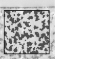
- the cross-sectional SEM photograph of the thickness direction of the glare-proof layer of the anti-glare film of Example 1 shows an example of the figure which binarized the fixed area.
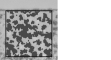
- the cross-sectional SEM photograph of the thickness direction of the anti-glare layer of the anti-glare film of Example 2 shows an example of a figure in which a certain area is binarized.
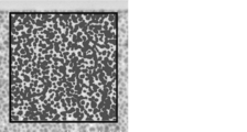
- the cross-sectional SEM photograph of the anti-glare layer thickness direction of the anti-glare film of Example 5 shows an example of a figure in which a certain area is binarized.
- the cross-sectional SEM photograph of the anti-glare layer thickness direction of the anti-glare film of the comparative example 3 shows an example of the figure which binarized a certain area. It is explanatory drawing of the measuring method of (theta) a.
- Example 1 An antiglare layer composition prepared by preparing a light transmissive substrate (thickness 40 ⁇ m, triacetyl cellulose resin film, Konica Minolta, KC4UYW) on one side of the light transmissive substrate with the composition shown below. 1 was applied so that the coating thickness was 6.0 ⁇ m (when dried) to form a coating film. Next, the formed coating film is dried in a heating oven at a temperature of 70 ° C. for 60 seconds, the solvent in the coating film is evaporated, and the coating film is irradiated with ultraviolet rays so that the irradiation dose becomes 120 mJ / cm 2. By curing, an antiglare layer was formed, and the antiglare film of Example 1 was produced.
- a light transmissive substrate thickness 40 ⁇ m, triacetyl cellulose resin film, Konica Minolta, KC4UYW
- MIBK methyl isobutyl ketone
- Example 2 An antiglare film was produced in the same manner as in Example 1 except that the antiglare layer composition 2 having the following composition was used instead of the antiglare layer composition 1.
- Product name V-8803 Average primary particle size 25 nm 36 parts by mass
- Organic filler A Sekisui Plastics Co., Ltd.
- Techpolymer SSX styrene-acrylic copolymer, average particle size 5.0 ⁇ m 1.52 20 parts by mass of organic filler B: Sekisui Plastics Co., Ltd.
- Example 3 An antiglare film was produced in the same manner as in Example 1 except that the antiglare layer composition 3 having the following composition was used instead of the antiglare layer composition 1.
- Isocyanuric acid EO-modified triacrylate Product name M-313 22 parts by mass Binder resin E: DNP Fine Chemicals PMMA polymer (weight average molecular weight 75000)
- Example 4 The same composition as in Example 1 except that the antiglare layer composition 4 having the following composition was used instead of the antiglare layer composition 1 and the antiglare layer was formed with a coating thickness of 3.0 ⁇ m (when dried). Thus, an antiglare film was produced.
- Product name V-8803 Average primary particle size 25 nm 40 parts by mass Organic filler D: SX series manufactured by Soken Chemical Co., Ltd., styrene beads, average particle size 3.5 ⁇ m Refractive index 1.59 1.25 Mass parts inorganic filler F: Amorphous silica manufactured by Dainichi Seika Co., Ltd., average particle size 1.5 ⁇ m
- Binder resin E PNP polymer (weight average molecular weight 75000) manufactured by DNP Fine Chemical Co., Ltd.
- HRAG acrylic 10 parts by mass Irgacure 184 6 parts by mass polyether-modified silicone manufactured by BASF Japan Oil: Momentive Performance Materials, Inc.
- TSF4460 0.1 parts by mass Toluene 60 parts by mass Methyl isobutyl ketone (MIBK) 40 parts by mass
- Example 5 An antiglare film was produced in the same manner as in Example 1 except that the antiglare layer composition 5 having the following composition was used instead of the antiglare layer composition 1.
- Example 6 An antiglare film was produced in the same manner as in Example 1 except that the antiglare layer composition 6 having the following composition was used instead of the antiglare layer composition 1.
- Product name V-8803 Average primary particle size 25 nm 45 parts by mass Organic filler B: Techpolymer SSX, styrene-acrylic copolymer manufactured by Sekisui Plastics Co., Ltd., average particle size 3.5 ⁇ m 1.52 part by mass Organic filler E: Techpolymer SSX, styrene-acrylic copolymer, Sekisui Plastics Co., Ltd., average particle size 3.5 ⁇ m, refractive index 1.50 11 parts by mass Binder resin A: Nippon Kayaku Co., Ltd.
- Example 7 An antiglare film was produced in the same manner as in Example 1 except that the antiglare layer composition 7 having the following composition was used instead of the antiglare layer composition 1.
- Product name V-8803 Average primary particle size 25 nm 60 parts by mass Organic filler B: Techpolymer SSX, styrene-acrylic copolymer manufactured by Sekisui Plastics Co., Ltd., average particle size 3.5 ⁇ m 1.52 part by mass Organic filler E: Techpolymer SSX, styrene-acrylic copolymer, Sekisui Plastics Co., Ltd., average particle size 3.5 ⁇ m, refractive index 1.50 11 parts by mass Binder resin A: Nippon Kayaku Co., Ltd.
- Example 1 In place of the antiglare layer composition 1, the antiglare layer composition 8 having the following composition was used, and the antiglare layer was prepared in the same manner as in Example 1 except that the coating thickness was 3.0 ⁇ m (when dried). A conductive film was prepared.
- Binder resin A Pentaerystol triacrylate manufactured by Nippon Kayaku Co., Ltd.
- Example 2 An antiglare film was produced in the same manner as in Example 1 except that the antiglare layer composition 9 having the following composition was used instead of the antiglare layer composition 1.
- ⁇ Anti-glare layer composition 9> Organic filler A: Sekisui Plastics Co., Ltd. Techpolymer SSX, styrene-acrylic copolymer, average particle size 5.0 ⁇ m Refractive index 1.52 20 parts by mass
- Organic filler B Sekisui Plastics Co., Ltd.
- Binder resin A Pentaerystol triacrylate manufactured by Nippon Kayaku Co., Ltd.
- Binder resin C Isocyanuric acid manufactured by Toa Gosei Co., Ltd.
- EO-modified triacrylate Product name M-313 22 parts by mass
- Binder resin E PMMA polymer (weight average molecular weight 75000) manufactured by DNP Fine Chemical Co., Ltd.
- Example 3 An antiglare film was produced in the same manner as in Example 1 except that the antiglare layer composition 10 having the following composition was used instead of the antiglare layer composition 1.
- Product name V-8803 Average primary particle size 25 nm 27 parts by mass
- Organic filler A Sekisui Plastics Co., Ltd.
- Techpolymer SSX styrene-acrylic copolymer, average particle size 5.0 ⁇ m 1.52 20 parts by mass of organic filler B: Sekisui Plastics Co., Ltd.
- Example 4 An antiglare film was produced in the same manner as in Example 1 except that the composition 11 for antiglare layer having the following composition was used instead of the composition 1 for antiglare layer.
- Product name V-8803 Average primary particle size 25 nm 65 parts by mass Organic filler B: Techpolymer SSX, styrene-acrylic copolymer manufactured by Sekisui Plastics Co., Ltd., average particle size 3.5 ⁇ m 1.52 part by mass Organic filler E: Techpolymer SSX, styrene-acrylic copolymer, Sekisui Plastics Co., Ltd., average particle size 3.5 ⁇ m, refractive index 1.50 11 parts by mass Binder resin A: Nippon Kayaku Co., Ltd.
- Binder resin D acrylic resin containing methacrylic acid manufactured by DIC, weight average molecular weight 8300
- Irgacure 184 6 parts by weight polyether manufactured by BASF Japan Modified silicone oil: Momentive Performance Materials, product name TSF 4460 0.1 parts by mass Toluene 60 parts by mass Methyl isobutyl ketone (MIBK) 40 parts by mass
- Comparative Example 5 An antiglare film was produced in the same manner as in Comparative Example 1 except that the coating thickness of the antiglare layer was 11.0 ⁇ m.
- Antiglare film was produced in the same manner as in Example 1 except that the antiglare layer composition 12 having the following composition was used instead of the antiglare layer composition 1.
- Organic filler A Sekisui Plastics Co., Ltd.
- Example 7 An antiglare film was produced in the same manner as in Example 1 except that the antiglare layer composition 13 having the following composition was used instead of the antiglare layer composition 1 and the film thickness was changed to 11.0 ⁇ m. .
- Techpolymer SSX styrene-acrylic copolymer, average particle size 5.0 ⁇ m Refractive index 1.52 20 parts by mass of organic filler B: Sekisui Plastics Co., Ltd.
- Example 8 An antiglare film was produced in the same manner as in Example 1 except that the antiglare layer composition 14 having the following composition was used instead of the antiglare layer composition 1 and the film thickness was changed to 3.0 ⁇ m. .
- ⁇ Anti-glare layer composition 14> Spherical silica: manufactured by JGC Catalysts & Chemicals Co., Ltd.
- ⁇ Pencil hardness> Each anti-glare film was conditioned for 2 hours under the conditions of a temperature of 25 ° C. and a relative humidity of 60%, and then JIS K5600-5 using a test pencil specified by JIS-S-6006 (hardness HB to 3H). -4 (1999), the pencil hardness of the surface on which the antiglare layer was formed was measured under a load of 4.9 N.
- ⁇ Abrasion resistance> The surface of the antiglare film, using a # 0000 steel wool (manufactured by Bonsuta Sales Co., Ltd.), 10 double rubs with friction load 4.9 N / cm 2 and 6.86N / cm 2, then the coating film The results were evaluated according to the following criteria. ⁇ : No scratch of the coating film at the friction load of 6.86N / cm 2 ⁇ : Friction load 4.9 N / cm 2 in no scratches coating, there scratches friction load 6.86N / cm 2 in the coating film ⁇ : Friction There is a scratch on the coating film at a load of 4.9 N / cm 2
- each antiglare film (side surface of the light transmissive substrate) is a transparent adhesive film for optical films (total light transmittance of 91% or more, haze of 0.3% or less, film thickness of 20 to 50 ⁇ m, for example, MHM series. : A sample bonded to a black acrylic plate by Niei Engineering Co., Ltd.) was placed on a horizontal plane, visually observed from various directions under a bright room condition of 1000 Lx, and evaluated according to the following evaluation criteria.
- ⁇ Coating adhesion> Put 100mm squares on the surface of each antiglare film (antiglare layer surface) with 1mm square grid cut, apply 24mm adhesive tape made by Nichiban Co., Ltd., and rub it with the back of the cutter knife. Rapid peeling was performed 5 times in the 90 ° direction, and the meshes where the coating film remained on the film surface were visually confirmed. The peeling along the cut line was not counted, and it was confirmed whether or not the inside of the square was peeled off. No peeling: The number of coating films remaining in a 100 square cell is 100 Exfoliation: The number of coating films remaining in a 100 square cell is less than 100
- ⁇ Mandrel test> Cut each anti-glare film into 2.5cm x 20cm square, wrap it around a mandrel rod with a different diameter manufactured by Toyo Seiki Co., Ltd. And visually confirmed with the transmitted light from the stand, the presence or absence of cracks in the antiglare layer was confirmed. In the evaluation, the value of the minimum diameter at which no cracks occurred was described.
- the antiglare films of the examples were excellent in all of physical properties and optical properties such as pencil hardness, scratch resistance, coating film adhesion, and crack prevention properties.
- none of the anti-glare films of Comparative Examples were good in all of pencil hardness, scratch resistance, coating film adhesion and optical properties.
- ⁇ Surface roughness (average interval of unevenness (Sm), arithmetic average roughness of unevenness (Ra), average inclination angle of unevenness ( ⁇ a))>
- the average spacing (Sm) of the irregularities on the surface of the antiglare layer, the arithmetic average roughness (Ra) of the irregularities, and the average inclination angle ( ⁇ a) of the irregularities was measured under the following conditions using a surface roughness measuring instrument: SE-3400 / manufactured by Kosaka Laboratory.
- the average interval (Sm) of unevenness and the arithmetic average roughness (Ra) of unevenness are values obtained by a method according to JIS B 0601-1994.
- the average inclination angle ( ⁇ a) of the concavo-convex portion is a value obtained by the definition described in the surface roughness measuring instrument: SE-3400 instruction manual (revised 1995.07.20) (Kosaka Laboratory Ltd.).
- the arc tangent ⁇ a tan ⁇ 1 (h 1 + h 2 + h 3 +) of the sum of the heights of the convex portions existing in the reference length L (h 1 + h 2 + h 3 +... + H n ) ... + h n ) / L ⁇ .
- Table 2 The results are shown in Table 2.
- the antiglare film of the present invention is a display such as a cathode ray tube display (CRT), a liquid crystal display (LCD), a plasma display (PDP), an electroluminescence display (ELD), a touch panel, electronic paper, a tablet PC, etc. It can be suitably used for a display.
- CTR cathode ray tube display
- LCD liquid crystal display
- PDP plasma display
- ELD electroluminescence display
- touch panel electronic paper
- tablet PC etc. It can be suitably used for a display.
Landscapes
- Physics & Mathematics (AREA)
- General Physics & Mathematics (AREA)
- Optics & Photonics (AREA)
- Chemical & Material Sciences (AREA)
- Nonlinear Science (AREA)
- Crystallography & Structural Chemistry (AREA)
- Mathematical Physics (AREA)
- Dispersion Chemistry (AREA)
- Optical Elements Other Than Lenses (AREA)
- Liquid Crystal (AREA)
- Laminated Bodies (AREA)
- Polarising Elements (AREA)
- Devices For Indicating Variable Information By Combining Individual Elements (AREA)
- Surface Treatment Of Optical Elements (AREA)
Abstract
Description
上記防眩層の厚み方向の断面における上記鎖状無機微粒子の面積率が40~80%であることが好ましい。
上記防眩層中の上記鎖状無機微粒子の充填率が40~150%であることが好ましい。
上記鎖状無機微粒子は、平均一次粒径1~90nmの球状の無機微粒子3~20個が連続して鎖状になったものであることが好ましい。
上記鎖状無機微粒子は、鎖状シリカであることが好ましい。
上記防眩層は、単層であることが好ましい。
上記防眩層の膜厚が3~10μmであることが好ましい。
上記防眩層は、更にフィラーを5~25質量%含むことが好ましい。
上記フィラーは、スチレン-アクリル共重合体ビーズ、ポリスチレンビーズ、及び、アクリルビーズからなる群より選択される少なくとも1種であることが好ましい。
また、本発明は、上述の防眩性フィルム、又は、上述の偏光板を備えることを特徴とする画像表示装置でもある。
以下、本発明を詳細に説明する。
このため、鉛筆硬度及び耐擦傷性が高く、防眩性に優れ、画像コントラストが高い防眩性フィルムとすることができる。
そして、鎖状シリカなど屈折率が低い鎖状無機微粒子の場合であれば、層表面の屈折率を下げ、外光の反射を軽減させて、見た目の黒さを向上させことができると考えられる。また、鎖状無機微粒子を使用すると、防眩層を形成するための防眩層用組成物の粘度が比較的高くなり、所望の凹凸形状の形成を制御し易く、優れた防眩性を付与することができる。
本発明の防眩層の層表面とは、最上層表面や基材側の最下層表面を含まない部分であり、最上層表面や、最下層表面より200nm離れた任意の領域である。
鎖状無機微粒子がシリカなど防眩層マトリックス樹脂より屈折率が低い無機微粒子の場合は、最上層表面にも、鎖状微粒子のみが密に存在しやすくなり、あたかも鎖状微粒子の1粒子の平均粒子径程度の膜厚の低屈折率層が形成されている状態になりやすく(図1~図4)、これが更に防眩層の反射率を低下することに効果があると考えている。防眩層は単層であるが、充填率で鎖状無機微粒子が存在することで、擬似低屈折率層が最表面に形成されることも本発明の特徴である。
なお、上記鎖状無機微粒子が、防眩層に連なって分散しているとは、鎖状無機微粒子が防眩層中に密に存在している(後述する面積率を満たす)状態、さらに好ましくは、防眩層内に鎖状無機微粒子の凝集塊(50~200nm角大)が複数形成され、これらの凝集塊が接触して網状構造若しくはこれに類似する構造を形成している状態をいう。
この凝集塊(50~200nm角大)は、鎖状に連なった無機微粒子が直線状に伸びた形状であっても、二次元的又は三次元的に湾曲した形状であっても構わない。よって、本発明の鎖状無機微粒子の定義:平均一次粒径1~90nmの球状の無機微粒子が3~20個連続して鎖状を形成していることと矛盾しない。
従って、鎖状無機微粒子が、防眩層中に密に存在していない状態(面積率を満たしていない状態)、鎖状無機微粒子の凝集体同士が粗に存在している状態(例えば、図4のように、面積率を満たさず、上記凝集塊同士が接触せずに、互いに離れている状態)を表すものではなく、図1のように面積率をみたす状態、さらに好ましくは図2及び図3のような面積率を満たし、かつ鎖状無機微粒子又は該鎖状無機微粒子の凝集塊同士が接触した状態を表す。
上記防眩層中の鎖状無機微粒子の分散状態は、防眩層の厚み方向の断面をSEM等で観察することにより確認することができる。
具体的には、上記鎖状無機微粒子は、平均一次粒径1~100nmの球状の無機微粒子3~20個が連続して鎖状になったものであることが好ましい。
上記鎖状無機微粒子の平均一次粒径及び個数が上述の範囲外であると、充分な鉛筆硬度を有する防眩層が得られないおそれがある。
上記鎖状無機微粒子は、鎖状に連なった無機微粒子が直線状に伸びた形状であっても、二次元的又は三次元的に湾曲した形状であっても構わない。
上記鎖状無機微粒子は、上記防眩層中で密に充填されているので、本発明の防眩性フィルムを断面観察した場合、20個を超える多数の上記球状の無機微粒子が連なって観察されることがある。このため上記鎖状無機微粒子は、本発明の防眩性フィルムの断面観察において、上記球状の無機微粒子3個以上が連続して鎖状になった状態で観察されるものである。本発明の平均一次粒径とは、SEMなどで断面観察した折に目視できる鎖状無機微粒子を構成する球状の1微粒子の任意の10個の平均粒径のことをいう。
上記鎖状シリカは、シリカ微粒子が連続して鎖状になったものをいい、直線状に伸びた形状、又は、二次元的若しくは三次元的に湾曲した形状のものを挙げることができる。
上記鎖状シリカの市販品としては、日揮触媒化成社製V-8803等を挙げることができる。
また、上記鎖状中空シリカを含有することにより、防眩層全体の屈折率を小さくして、防眩性フィルムの反射率を低下させることができる。
上記面積率が30%未満であると、鉛筆硬度及び耐擦傷性が不充分となる。鉛筆硬度がより優れることから、上記面積率の下限は、40%であることが好ましい。
上記面積率が94%を超えると、防眩層と光透過性基材との密着性が低下したり、本発明の防眩性フィルムの硬度は増すが、もろくなってしまうため、防眩性フィルムの製造時や使用時にクラック等が発生しやすくなる。また、防眩層の製造が困難となり、更に、製造コストの上昇につながる。クラック発生防止の点から、上記面積率の上限は、80%が好ましい。
例えば、以下の方法で測定することができる。
(1)SEM断面写真
ミクロトームを用いて光学積層体を切削し、超薄切片サンプルを作成し、日立協和エンジニアリング株式会社製 デジタル走査型電子顕微鏡(S-4800)を用いて、倍率50000倍(加速電圧 30.0kV、エミッション電流 10μA)にてSEM断面写真を得る。
(2)面積率測定
SEM断面写真のデジタルデータから、画像解析ソフトWin Roof(三谷商事株式会社ビジュアルシステム部製)を用いて画像の二値化を行い、測定して得ることができる。
SEM断面写真には、鎖状無機微粒子が確認でき、この鎖状無機微粒子部分をソフト上で選択して着色し(二値化)、選択部分の面積を求めるとよい。
40%未満であると、充分な鉛筆硬度及び耐擦傷性を有する防眩層が得られないおそれがある。また、見た目の黒さを感じられず、さらには所望の凹凸形状の形成の制御効果が劣るおそれがある。150%を超えると、バインダー樹脂の割合が少なくなりすぎるため、基材との密着が損なわれる等のおそれがある。上記鎖状無機微粒子の充填率は、下限が50%であることがより好ましく、上限が90%であることがより好ましい。
なお、上記充填率は、防眩層中の樹脂の質量(A)に対する鎖状無機微粒子の質量(B)の百分率(B/A)である。
上記フィラーを含有させることにより、防眩層に表面凹凸形状を形成し、光拡散や内部散乱による防眩性を付与することができる。
上記フィラーは微粒子であり、形状は、真球状、楕円状、不定形など、特に限定されない。また、上記フィラーとしては、無機系、有機系の微粒子を使用することができ、好ましくは透明性の微粒子がよい。
無機フィラーとしては、不定形シリカ、球状等、ある特定形状を持った無機シリカビーズ等を挙げることができる。
上記フィラーは、単独で含有していてもよいし、2種以上含有していてもよい。
なかでも、上記フィラーとしては、スチレン-アクリル共重合体ビーズ、ポリスチレンビーズ、及び、アクリルビーズからなる群より選択される少なくとも1種であることが好ましい。また、表面凹凸の形成及び屈折率の調整が容易になる点で、スチレン-アクリル共重合体ビーズであることがより好ましい。
また、コントラストを高める点で、上記バインダー樹脂との屈折率差が0.05以内のスチレン-アクリル共重合体ビーズを、バインダー樹脂及び鎖状無機微粒子の合計100質量部に対して、20質量部以下含有させることが好ましい。
屈折率は、材料そのものや、例えば、防眩性フィルムを製造後、その断面を出すことによって、フィラーやバインダーの断面を出したり、フィラーやバインダー片を削って取り出すことにより、アッベ屈折計で直接測定するか、ベッケ法などカーギル試薬を用いる方法、または防眩性フィルムを直接、レーザー干渉による測定、分光反射スペクトルや分光エリプソメトリーを測定するなどして定量的に測定できる。
防眩層用組成物を塗工、硬化したのちの防眩性フィルム中の上記フィラーの粒径は、光学顕微鏡で透過観察を行い、200倍から1000倍の倍率において観察できる粒径を、解析ソフトなどを用いて測定が可能である。その場合、10粒子以上の粒径を観察測定し、平均した値を平均粒径とする。
上記フィラーの含有量は、7~20質量%であることがより好ましい。
上記レベリング剤としては、例えば、フッ素系レベリング剤、シリコーン系レベリング剤、アクリル系レベリング剤等を挙げることができる。なかでも、少量の添加で効果がある点で、シリコーン系レベリング剤が好ましい。
なかでも、上記防眩層の凹凸形状は、上記フィラーを含む防眩層用組成物により形成したものであることが好ましい。
上記防眩層の表面凹凸形状は、防眩性が発揮され得る凹凸形状であれば特に限定されず、公知の凹凸形状であればよい。
上記層厚みは、防眩性フィルムの断面を、電子顕微鏡(SEM、TEM、STEM)で観察することにより任意の10点の厚みを測定して得られた平均値である。
上記混合分散は、ペイントシェーカー、ビーズミル、ニーダー等の公知の装置を使用して行うとよい。
上記範囲の粘度であると、所望の凹凸形状を有する防眩層を好適に形成することができる。
上記紫外線を照射する場合は、40~300mJ/cm2の紫外線を照射する方法が挙げられる。
上記光透過性基材は、平滑性、耐熱性を備え、機械的強度とに優れたものが好ましい。
上記光透過性基材を形成する材料の具体例としては、ポリエステル(ポリエチレンテレフタレート、ポリエチレンナフタレート)、セルローストリアセテート、セルロースジアセテート、セルロースアセテートブチレート、ポリアミド、ポリイミド、ポリエーテルスルフォン、ポリスルフォン、ポリプロピレン、ポリメチルペンテン、ポリ塩化ビニル、ポリビニルアセタール、ポリエーテルケトン、ポリメタクリル酸メチル、ポリカーボネート、又は、ポリウレタン等の熱可塑性樹脂が挙げられ、好ましくはポリエステル(ポリエチレンテレフタレート、ポリエチレンナフタレート)、トリアセチルセルロースが挙げられる。
また、上記光透過性基材は、その上に防眩層を形成するのに際して、接着性向上のために、コロナ放電処理、酸化処理等の物理的な処理のほか、アンカー剤もしくはプライマーと呼ばれる塗料の塗布を予め行ってもよい。
上記ヘイズは、ヘーズ・透過率計HM-150(村上色彩技術研究所製)を用いてJISK-7136に準拠した方法により測定することができる。ヘイズは基材を光源側に向けて測定する。
20%を超えると、ディスプレイ表面に装着した場合において、内部散乱が強すぎたり、迷光を生じることに繋がり、色再現性や視認性を損なうおそれがある他、所望のコントラストが得られないおそれがある。
表面を平坦にした防眩性フィルムは、表面凹凸によるヘイズをもたず、内部ヘイズだけを持つ状態となっている。このヘイズを、内部ヘイズとして求めることができる。
なお、ヘイズ値は、JIS K-7136に従って測定することができる。測定に使用する機器としては、ヘーズ・透過率計 HM-150(村上色彩技術研究所製)が挙げられる。ヘイズは、基材を光源に向けて測定する。
このため、本発明の防眩性フィルムは、陰極線管表示装置(CRT)、液晶ディスプレイ(LCD)、プラズマディスプレイ(PDP)、エレクトロルミネッセンスディスプレイ(ELD)、タッチパネル、電子ペーパー、タブレットPC等のディスプレイ、特に高精細化ディスプレイに好適に使用することができる。
なお、文中、「部」又は「%」とあるのは特に断りのない限り、質量基準である。
光透過性基材(厚み40μm、トリアセチルセルロース樹脂フィルム、コニカミノルタ社製、KC4UYW)を準備し、該光透過性基材の片面に、下記に示した組成で調製した防眩層用組成物1を、塗工厚みが6.0μm(乾燥時)となるように塗布し、塗膜を形成した。次いで、形成した塗膜を温度70℃の熱オーブン中で60秒間乾燥し、塗膜中の溶剤を蒸発させ、塗膜に紫外線を照射線量が120mJ/cm2になるよう照射して塗膜を硬化させることにより、防眩層を形成し、実施例1の防眩性フィルムを作製した。
<防眩層用組成物1>
鎖状シリカ:日揮触媒化成社製 製品名V-8803 平均一次粒径25nm 31質量部
有機フィラーA:積水化成品工業社製テクポリマーSSX、スチレン-アクリル共重合体、平均粒径5.0μm 屈折率1.52 20質量部
有機フィラーB:積水化成品工業社製テクポリマーSSX、スチレン-アクリル共重合体、平均粒径3.5μm 屈折率1.52 3質量部
バインダー樹脂A:日本化薬社製ペンタエリストールトリアクリレート 製品名PETA 36質量部
バインダー樹脂C:東亜合成社製イソシアヌル酸EO変性トリアクリレート
製品名M-313 22質量部
バインダー樹脂E:DNPファインケミカル社製PMMAポリマー(重量平均分子量75000)製品名HRAGアクリル 11質量部
イルガキュア184:BASFジャパン社製 6質量部
ポリエーテル変性シリコーンオイル:モメンティブ パフォーマンス マテリアルズ社製 製品名TSF4460 0.1質量部
トルエン 60質量部
メチルイソブチルケトン(MIBK) 40質量部
防眩層用組成物1の代わりに、下記組成の防眩層用組成物2を用いた点以外は、実施例1と同様にして、防眩性フィルムを作製した。
<防眩層用組成物2>
鎖状シリカ:日揮触媒化成社製 製品名V-8803 平均一次粒径25nm 36質量部
有機フィラーA:積水化成品工業社製テクポリマーSSX、スチレン-アクリル共重合体、平均粒径5.0μm 屈折率1.52 20質量部
有機フィラーB:積水化成品工業社製テクポリマーSSX、スチレン-アクリル共重合体、平均粒径3.5μm 屈折率1.52 3質量部
バインダー樹脂A:日本化薬社製ペンタエリストールトリアクリレート 製品名PETA 31質量部
バインダー樹脂C:東亜合成社製イソシアヌル酸EO変性トリアクリレート
製品名M-313 22質量部
バインダー樹脂E:DNPファインケミカル社製PMMAポリマー(重量平均分子量75000)製品名HRAGアクリル 11質量部
イルガキュア184:BASFジャパン社製 6質量部
ポリエーテル変性シリコーンオイル:モメンティブ パフォーマンス マテリアルズ社製 製品名TSF4460 0.1質量部
トルエン 60質量部
メチルイソブチルケトン(MIBK) 40質量部
防眩層用組成物1の代わりに、下記組成の防眩層用組成物3を用いた点以外は、実施例1と同様にして、防眩性フィルムを作製した。
<防眩層用組成物3>
鎖状シリカ:日揮触媒化成社製 製品名V-8803 平均一次粒径25nm 36質量部
有機フィラーA:積水化成品工業社製テクポリマーSSX、スチレン-アクリル共重合体、平均粒径5.0μm 屈折率1.52 11質量部
有機フィラーC:積水化成品工業社製テクポリマーSSX、スチレン-アクリル共重合体、平均粒径3.5μm 屈折率1.55 6質量部
バインダー樹脂A:日本化薬社製ペンタエリストールトリアクリレート 製品名PETA 31質量部
バインダー樹脂C:東亜合成社製イソシアヌル酸EO変性トリアクリレート
製品名M-313 22質量部
バインダー樹脂E:DNPファインケミカル社製PMMAポリマー(重量平均分子量75000)製品名HRAGアクリル 11質量部
イルガキュア184:BASFジャパン社製 6質量部
ポリエーテル変性シリコーンオイル:モメンティブ パフォーマンス マテリアルズ社製 製品名TSF4460 0.1質量部
トルエン 60質量部
メチルイソブチルケトン(MIBK) 40質量部
防眩層用組成物1の代わりに、下記組成の防眩層用組成物4を用い、塗工厚み3.0μm(乾燥時)で防眩層を形成した点以外は、実施例1と同様にして、防眩性フィルムを作製した。
<防眩層用組成物4>
鎖状シリカ:日揮触媒化成社製 製品名V-8803 平均一次粒径25nm 40質量部
有機フィラーD:綜研化学社製SXシリーズ、スチレンビーズ、平均粒径3.5μm 屈折率1.59 1.25質量部
無機フィラーF:大日精化社製不定形シリカ、平均粒径1.5μm 製品名EXG40-77(D-30M) 10質量部
バインダー樹脂A:日本化薬社製ペンタエリストールトリアクリレート 製品名PETA 40質量部
バインダー樹脂C:東亜合成社製イソシアヌル酸EO変性トリアクリレート
製品名M-313 10質量部
バインダー樹脂E:DNPファインケミカル社製PMMAポリマー(重量平均分子量75000)製品名HRAGアクリル 10質量部
イルガキュア184:BASFジャパン社製 6質量部
ポリエーテル変性シリコーンオイル:モメンティブ パフォーマンス マテリアルズ社製 製品名TSF4460 0.1質量部
トルエン 60質量部
メチルイソブチルケトン(MIBK) 40質量部
防眩層用組成物1の代わりに、下記組成の防眩層用組成物5を用いた点以外は、実施例1と同様にして、防眩性フィルムを作製した。
<防眩層用組成物5>
鎖状シリカ:日揮触媒化成社製 製品名V-8803 平均一次粒径25nm 40質量部
有機フィラーB:積水化成品工業社製テクポリマーSSX、スチレン-アクリル共重合体、平均粒径3.5μm 屈折率1.52 1質量部
有機フィラーE:積水化成品工業社製テクポリマーSSX、スチレン-アクリル共重合体、平均粒径3.5μm 屈折率1.50 11質量部
バインダー樹脂A:日本化薬社製ペンタエリストールトリアクリレート 製品名PETA 30質量部
バインダー樹脂D:DIC社製メタクリル酸を含むアクリル樹脂、重量平均分子量8300 製品名RS29-266 30質量部
イルガキュア184:BASFジャパン社製 6質量部
ポリエーテル変性シリコーンオイル:モメンティブ パフォーマンス マテリアルズ社製 製品名TSF4460 0.1質量部
トルエン 60質量部
メチルイソブチルケトン(MIBK) 40質量部
防眩層用組成物1の代わりに、下記組成の防眩層用組成物6を用いた点以外は、実施例1と同様にして、防眩性フィルムを作製した。
<防眩層用組成物6>
鎖状シリカ:日揮触媒化成社製 製品名V-8803 平均一次粒径25nm 45質量部
有機フィラーB:積水化成品工業社製テクポリマーSSX、スチレン-アクリル共重合体、平均粒径3.5μm 屈折率1.52 1質量部
有機フィラーE:積水化成品工業社製テクポリマーSSX、スチレン-アクリル共重合体、平均粒径3.5μm 屈折率1.50 11質量部
バインダー樹脂A:日本化薬社製ペンタエリストールトリアクリレート 製品名PETA 25質量部
バインダー樹脂D:DIC社製メタクリル酸を含むアクリル樹脂、重量平均分子量8300 製品名RS29-266 30質量部
イルガキュア184:BASFジャパン社製 6質量部
ポリエーテル変性シリコーンオイル:モメンティブ パフォーマンス マテリアルズ社製 製品名TSF4460 0.1質量部
トルエン 60質量部
メチルイソブチルケトン(MIBK) 40質量部
防眩層用組成物1の代わりに、下記組成の防眩層用組成物7を用いた点以外は、実施例1と同様にして、防眩性フィルムを作製した。
<防眩層用組成物7>
鎖状シリカ:日揮触媒化成社製 製品名V-8803 平均一次粒径25nm 60質量部
有機フィラーB:積水化成品工業社製テクポリマーSSX、スチレン-アクリル共重合体、平均粒径3.5μm 屈折率1.52 1質量部
有機フィラーE:積水化成品工業社製テクポリマーSSX、スチレン-アクリル共重合体、平均粒径3.5μm 屈折率1.50 11質量部
バインダー樹脂A:日本化薬社製ペンタエリストールトリアクリレート 製品名PETA 10質量部
バインダー樹脂D:DIC社製メタクリル酸を含むアクリル樹脂、重量平均分子量8300 製品名RS29-266 30質量部
イルガキュア184:BASFジャパン社製 6質量部
ポリエーテル変性シリコーンオイル:モメンティブ パフォーマンス マテリアルズ社製 製品名TSF4460 0.1質量部
トルエン 60質量部
メチルイソブチルケトン(MIBK) 40質量部
防眩層用組成物1の代わりに、下記組成の防眩層用組成物8を用い、塗工厚み3.0μm(乾燥時)とした点以外は、実施例1と同様にして、防眩性フィルムを作製した。
<防眩層用組成物8>
無機フィラーF:大日精化社製不定形シリカ、平均粒径1.5μm 製品名EXG40-77(D-30M) 9質量部
バインダー樹脂A:日本化薬社製ペンタエリストールトリアクリレート 製品名PETA 100質量部
イルガキュア184:BASFジャパン社製 6質量部
ポリエーテル変性シリコーンオイル:モメンティブ パフォーマンス マテリアルズ社製 製品名TSF4460 0.1質量部
トルエン 80質量部
メチルイソブチルケトン(MIBK) 20質量部
防眩層用組成物1の代わりに、下記組成の防眩層用組成物9を用いた点以外は、実施例1と同様にして、防眩性フィルムを作製した。
<防眩層用組成物9>
有機フィラーA:積水化成品工業社製テクポリマーSSX、スチレン-アクリル共重合体、平均粒径5.0μm 屈折率1.52 20質量部
有機フィラーB:積水化成品工業社製テクポリマーSSX、スチレン-アクリル共重合体、平均粒径3.5μm 屈折率1.52 3質量部
バインダー樹脂A:日本化薬社製ペンタエリストールトリアクリレート 製品名PETA 67質量部
バインダー樹脂C:東亜合成社製イソシアヌル酸EO変性トリアクリレート
製品名M-313 22質量部
バインダー樹脂E:DNPファインケミカル社製PMMAポリマー(重量平均分子量75000)製品名HRAGアクリル 11質量部
イルガキュア184:BASFジャパン社製 6質量部
ポリエーテル変性シリコーンオイル:モメンティブ パフォーマンス マテリアルズ社製 製品名TSF4460 0.1質量部
トルエン 60質量部
メチルイソブチルケトン(MIBK) 40質量部
防眩層用組成物1の代わりに、下記組成の防眩層用組成物10を用いた点以外は、実施例1と同様にして、防眩性フィルムを作製した。
<防眩層用組成物10>
鎖状シリカ:日揮触媒化成社製 製品名V-8803 平均一次粒径25nm 27質量部
有機フィラーA:積水化成品工業社製テクポリマーSSX、スチレン-アクリル共重合体、平均粒径5.0μm 屈折率1.52 20質量部
有機フィラーB:積水化成品工業社製テクポリマーSSX、スチレン-アクリル共重合体、平均粒径3.5μm 屈折率1.52 3質量部
バインダー樹脂A:日本化薬社製ペンタエリストールトリアクリレート 製品名PETA 40質量部
バインダー樹脂C:東亜合成社製イソシアヌル酸EO変性トリアクリレート
製品名M-313 22質量部
バインダー樹脂E:DNPファインケミカル社製PMMAポリマー(重量平均分子量75000)製品名HRAGアクリル 11質量部
イルガキュア184:BASFジャパン社製 6質量部
ポリエーテル変性シリコーンオイル:モメンティブ パフォーマンス マテリアルズ社製 製品名TSF4460 0.1質量部
トルエン 60質量部
メチルイソブチルケトン(MIBK) 40質量部
防眩層用組成物1の代わりに、下記組成の防眩層用組成物11を用いた点以外は、実施例1と同様にして、防眩性フィルムを作製した。
<防眩層用組成物11>
鎖状シリカ:日揮触媒化成社製 製品名V-8803 平均一次粒径25nm 65質量部
有機フィラーB:積水化成品工業社製テクポリマーSSX、スチレン-アクリル共重合体、平均粒径3.5μm 屈折率1.52 1質量部
有機フィラーE:積水化成品工業社製テクポリマーSSX、スチレン-アクリル共重合体、平均粒径3.5μm 屈折率1.50 11質量部
バインダー樹脂A:日本化薬社製ペンタエリストールトリアクリレート 製品名PETA 5質量部
バインダー樹脂D:DIC社製メタクリル酸を含むアクリル樹脂、重量平均分子量8300 製品名RS29-266 30質量部
イルガキュア184:BASFジャパン社製 6質量部
ポリエーテル変性シリコーンオイル:モメンティブ パフォーマンス マテリアルズ社製 製品名TSF4460 0.1質量部
トルエン 60質量部
メチルイソブチルケトン(MIBK) 40質量部
防眩層の塗工厚みを11.0μmとした点以外は、比較例1と同様にして、防眩性フィルムを作製した。
防眩層用組成物1の代わりに、下記組成の防眩層用組成物12を用いた点以外は、実施例1と同様にして、防眩性フィルムを作製した。
<防眩層用組成物12>
球状シリカ:日揮触媒化成社製 製品名DP-1117SIV 平均一次粒径25nm 31質量部
有機フィラーA:積水化成品工業社製テクポリマーSSX、スチレン-アクリル共重合体、平均粒径5.0μm 屈折率1.52 20質量部
有機フィラーB:積水化成品工業社製テクポリマーSSX、スチレン-アクリル共重合体、平均粒径3.5μm 屈折率1.52 3質量部
バインダー樹脂A:日本化薬社製ペンタエリストールトリアクリレート 製品名PETA 36質量部
バインダー樹脂C:東亜合成社製イソシアヌル酸EO変性トリアクリレート
製品名M-313 22質量部
バインダー樹脂E:DNPファインケミカル社製PMMAポリマー(重量平均分子量75000)製品名HRAGアクリル 11質量部
イルガキュア184:BASFジャパン社製 6質量部
ポリエーテル変性シリコーンオイル:モメンティブ パフォーマンス マテリアルズ社製 製品名TSF4460 0.1質量部
トルエン 60質量部
メチルイソブチルケトン(MIBK) 40質量部
防眩層用組成物1の代わりに、下記組成の防眩層用組成物13を用い、膜厚を11.0μmにした以外は、実施例1と同様にして、防眩性フィルムを作製した。
<防眩層用組成物13>
球状シリカ:日揮触媒化成社製 製品名DP-1117SIV 平均一次粒径25nm 40質量部
有機フィラーA:積水化成品工業社製テクポリマーSSX、スチレン-アクリル共重合体、平均粒径5.0μm 屈折率1.52 20質量部
有機フィラーB:積水化成品工業社製テクポリマーSSX、スチレン-アクリル共重合体、平均粒径3.5μm 屈折率1.52 3質量部
バインダー樹脂A:日本化薬社製ペンタエリストールトリアクリレート 製品名PETA 36質量部
バインダー樹脂C:東亜合成社製イソシアヌル酸EO変性トリアクリレート
製品名M-313 22質量部
バインダー樹脂E:DNPファインケミカル社製PMMAポリマー(重量平均分子量75000)製品名HRAGアクリル 11質量部
イルガキュア184:BASFジャパン社製 6質量部
ポリエーテル変性シリコーンオイル:モメンティブ パフォーマンス マテリアルズ社製 製品名TSF4460 0.1質量部
トルエン 60質量部
メチルイソブチルケトン(MIBK) 40質量部
防眩層用組成物1の代わりに、下記組成の防眩層用組成物14を用い、膜厚を3.0μmにした以外は、実施例1と同様にして、防眩性フィルムを作製した。
<防眩層用組成物14>
球状シリカ:日揮触媒化成社製 製品名DP-1117SIV 平均一次粒径25nm 65質量部
有機フィラーB:積水化成品工業社製テクポリマーSSX、スチレン-アクリル共重合体、平均粒径3.5μm 屈折率1.52 1質量部
有機フィラーE:積水化成品工業社製テクポリマーSSX、スチレン-アクリル共重合体、平均粒径3.5μm 屈折率1.50 11質量部
バインダー樹脂A:日本化薬社製ペンタエリストールトリアクリレート 製品名PETA 5質量部
バインダー樹脂D:DIC社製メタクリル酸を含むアクリル樹脂、重量平均分子量8300 製品名RS29-266 30質量部
イルガキュア184:BASFジャパン社製 6質量部
ポリエーテル変性シリコーンオイル:モメンティブ パフォーマンス マテリアルズ社製 製品名TSF4460 0.1質量部
トルエン 60質量部
メチルイソブチルケトン(MIBK) 40質量部
<面積率>
各防眩性フィルムについての、防眩層の厚み方向の断面における鎖状無機微粒子の面積率について、SEMによる断面写真から、画像解析ソフト画像解析ソフトWin Roof(三谷商事社ビジュアルシステム部製)によって断面を測定し、画像の2値化(鎖状微粒子の存在量を面積化する)を行い、測定した。なお、上記面積率は、上記防眩層断面において任意で5点測定し、それぞれ得られた値の平均値とした。また、図1に実施例1の、図2に実施例2の、図3に実施例5の、図4に比較例3の、防眩層の厚み方向の断面のSEM写真において2値化した図の一例を示した。これらの図は、いずれも倍率が5万倍の断面写真で、実線で囲まれた領域は1μm2である。ただし、有機粒子の存在しないところを選択し、かつ、最表面を含まず、深さ方向1.5μmの範囲内から、任意の5点を選択した。
各防眩性フィルムを、温度25℃、相対湿度60%の条件で2時間調湿した後、JIS-S-6006が規定する試験用鉛筆(硬度HB~3H)を用いて、JIS K5600-5-4(1999)が規定する鉛筆硬度評価方法に従い、4.9Nの荷重にて、防眩層が形成された表面の鉛筆硬度を測定した。
防眩性フィルムの表面を、#0000番のスチールウール(ボンスター販売株式会社製)を用いて、摩擦荷重4.9N/cm2及び6.86N/cm2で10往復摩擦し、その後の塗膜の剥がれの有無を目視し、結果を下記の基準にて評価した。
◎:摩擦荷重6.86N/cm2で塗膜の傷なし
○:摩擦荷重4.9N/cm2では塗膜の傷なし、摩擦荷重6.86N/cm2では塗膜の傷あり
×:摩擦荷重4.9N/cm2で塗膜の傷あり
各防眩性フィルムのヘイズについて、ヘイズメーター(村上色彩技術研究所製、製品番号;HM-150)を用いてJIS K-7136(ヘイズ)に準拠した方法により測定した。内部ヘイズについては、上述した方法により測定した。
各防眩性フィルムの裏面(光透過性基材側面)を、光学フィルム用透明粘着フィルム(全光線透過率91%以上、ヘイズ0.3%以下、膜厚20~50μmの製品、例えばMHMシリーズ:日栄加工(株)製など)で黒アクリル板に貼合した試料を水平面に置き、1000Lxの明室条件で目視にて様々な方向から観察し、下記の評価基準で評価した。
◎:十分な防眩があるが、白茶けておらず、黒くしまって見える
○:十分な防眩があり、やや白茶けるが、黒くしまって見える
×:十分な防眩があるが、全体的に白茶けている
-:所望の凹凸形成ができておらず防眩性がないため、対象外
各防眩性フィルムの表面(防眩層表面)に1mm角碁盤目カットにて、100升の升目を入れ、ニチバン社製工業用24mmの粘着テープを貼り、カッターナイフの背で擦って密着させ90°方向に5回急速剥離を行い、塗膜がフィルム表面に残っている升目を目視確認した。切り込み線に沿った剥がれは、カウントせず、升目の中が剥がれているかどうか確認した。
剥がれなし:100升の升目中に残っている塗膜の数が100
剥がれあり:100升の升目中に残っている塗膜の数が100未満
各防眩性フィルムを2.5cm×20cm角に切り取り、東洋精機社製の径の異なるマンドレル棒に、防眩層を外側にしてマンドレル棒に巻きつけた後、試験後のサンプルを暗室環境下にてスタンド透過光で目視確認し、防眩層のひび割れ(クラック)の有無を確認した。
なお評価においては、クラックが発生しなかった最小の径の値を記載した。

実施例1及び2、比較例3の防眩性フィルムについて、防眩層表面の凹凸の平均間隔(Sm)、凹凸の算術平均粗さ(Ra)、及び、凹凸部の平均傾斜角(θa)を、表面粗さ測定器:SE-3400/株式会社小坂研究所製を用い、以下の条件で測定した。
なお、凹凸の平均間隔(Sm)及び凹凸の算術平均粗さ(Ra)は、JIS B 0601-1994に準拠する方法で得た値である。凹凸部の平均傾斜角(θa)は、表面粗さ測定器:SE-3400 取り扱い説明書(1995.07.20改訂)(株式会社小坂研究所)に記載の定義により得た値であり、図5に示すように、基準長さLに存在する凸部高さの和(h1+h2+h3+・・・+hn)のアークタンジェント{θa=tan-1(h1+h2+h3+・・・+hn)/L}で求めたものである。結果を表2に示す。結果、鎖状微粒子の増量に伴い、θaが大きくなる等鎖状微粒子が凸凹形状に寄与し、耐擦傷性を向上させつつ、所望の防眩性の付与に寄与することがわかった。
<測定条件>
(1)表面粗さ検出部の触針:
型番/SE2555N(2μ触針)、株式会社小坂研究所製
(先端曲率半径2μm/頂角:90度/材質:ダイヤモンド)
(2)表面粗さ測定器の測定条件:
基準長さ(粗さ曲線のカットオフ値λc):0.8mm
評価長さ(基準長さ(カットオフ値λc)×5):4.0mm
触針の送り速さ:0.1mm/s

Claims (11)
- 光透過性基材と、前記光透過性基材の少なくとも一方の面上に、表面に凹凸形状を有する防眩層とを有する防眩性フィルムであって、
前記防眩層は、鎖状無機微粒子を含有し、
前記防眩層の厚み方向の断面における前記鎖状無機微粒子の面積率が30~94%である
ことを特徴とする防眩性フィルム。 - 防眩層の厚み方向の断面における鎖状無機微粒子の面積率が40~80%である請求項1記載の防眩性フィルム。
- 防眩層中の鎖状無機微粒子の充填率が40~150%である請求項1又は2記載の防眩性フィルム。
- 鎖状無機微粒子は、平均一次粒径1~90nmの球状の無機微粒子3~20個が連続して鎖状になったものである請求項1、2又は3記載の防眩性フィルム。
- 鎖状無機微粒子は、鎖状シリカである請求項1、2、3又は4記載の防眩性フィルム。
- 防眩層は、単層である請求項1、2、3、4又は5記載の防眩性フィルム。
- 防眩層の膜厚が3~10μmである請求項1、2、3、4、5又は6記載の防眩性フィルム。
- 防眩層は、更にフィラーを5~25質量%含む請求項1、2、3、4、5、6又は7記載の防眩性フィルム。
- フィラーは、スチレン-アクリル共重合体ビーズ、ポリスチレンビーズ、及び、アクリルビーズからなる群より選択される少なくとも1種である請求項8記載の防眩性フィルム。
- 偏光素子を備えてなる偏光板であって、
前記偏光素子の表面に請求項1、2、3、4、5、6、7、8又は9記載の防眩性フィルムを備えることを特徴とする偏光板。 - 請求項1、2、3、4、5、6、7、8若しくは9記載の防眩性フィルム、又は、請求項10記載の偏光板を備えることを特徴とする画像表示装置。
Priority Applications (4)
| Application Number | Priority Date | Filing Date | Title |
|---|---|---|---|
| JP2013525744A JP6213241B2 (ja) | 2011-07-26 | 2012-07-25 | 防眩性フィルム、偏光板及び画像表示装置 |
| KR1020147002022A KR101920523B1 (ko) | 2011-07-26 | 2012-07-25 | 방현성 필름, 편광판 및 화상 표시 장치 |
| US14/234,310 US10254444B2 (en) | 2011-07-26 | 2012-07-25 | Anti-glare film, polarizer and image display device |
| CN201280028137.7A CN103620449B (zh) | 2011-07-26 | 2012-07-25 | 防眩性膜、偏振片和图像显示装置 |
Applications Claiming Priority (2)
| Application Number | Priority Date | Filing Date | Title |
|---|---|---|---|
| JP2011-163692 | 2011-07-26 | ||
| JP2011163692 | 2011-07-26 |
Publications (1)
| Publication Number | Publication Date |
|---|---|
| WO2013015332A1 true WO2013015332A1 (ja) | 2013-01-31 |
Family
ID=47601170
Family Applications (1)
| Application Number | Title | Priority Date | Filing Date |
|---|---|---|---|
| PCT/JP2012/068879 Ceased WO2013015332A1 (ja) | 2011-07-26 | 2012-07-25 | 防眩性フィルム、偏光板及び画像表示装置 |
Country Status (6)
| Country | Link |
|---|---|
| US (1) | US10254444B2 (ja) |
| JP (2) | JP6213241B2 (ja) |
| KR (1) | KR101920523B1 (ja) |
| CN (1) | CN103620449B (ja) |
| TW (1) | TWI534482B (ja) |
| WO (1) | WO2013015332A1 (ja) |
Cited By (13)
| Publication number | Priority date | Publication date | Assignee | Title |
|---|---|---|---|---|
| JP2013186236A (ja) * | 2012-03-07 | 2013-09-19 | Nippon Zeon Co Ltd | ハードコートフィルム |
| JP2014162889A (ja) * | 2013-02-27 | 2014-09-08 | Lintec Corp | コーティング組成物およびコーティングフィルム |
| JP2014232276A (ja) * | 2013-05-30 | 2014-12-11 | リンテック株式会社 | 防眩性ハードコートフィルム |
| WO2015163330A1 (ja) * | 2014-04-23 | 2015-10-29 | 旭硝子株式会社 | アンチグレア層付き基材および物品 |
| WO2015163328A1 (ja) * | 2014-04-23 | 2015-10-29 | 大日本印刷株式会社 | 積層体の製造方法、積層体、偏光板、画像表示装置及び画像表示装置の視認性改善方法 |
| CN106415333A (zh) * | 2014-03-14 | 2017-02-15 | 日本电气硝子株式会社 | 显示器的罩部件及其制造方法 |
| JP2017061701A (ja) * | 2016-11-04 | 2017-03-30 | リンテック株式会社 | コーティング組成物およびコーティングフィルム |
| WO2021095745A1 (ja) * | 2019-11-11 | 2021-05-20 | 日東電工株式会社 | 防眩性フィルム、防眩性フィルムの設計方法、防眩性フィルムの製造方法、光学部材および画像表示装置 |
| JP2021076750A (ja) * | 2019-11-11 | 2021-05-20 | 日東電工株式会社 | 防眩性フィルム、防眩性フィルムの設計方法、防眩性フィルムの製造方法、光学部材および画像表示装置 |
| JP2021525396A (ja) * | 2019-01-08 | 2021-09-24 | エルジー・ケム・リミテッド | 光学積層体、偏光板、およびディスプレイ装置 |
| JP2024542339A (ja) * | 2022-10-20 | 2024-11-15 | 寧波甬安光科新材料科技有限公司 | ディスプレイ用のアンチグレア反射防止膜 |
| WO2025023326A1 (ja) * | 2023-07-27 | 2025-01-30 | 大日本印刷株式会社 | 防眩シート、シート物品、偏光板、表示装置、及び防眩物品 |
| WO2025023327A1 (ja) * | 2023-07-27 | 2025-01-30 | 大日本印刷株式会社 | 防眩シート、シート物品、偏光板、表示装置、及び防眩物品 |
Families Citing this family (7)
| Publication number | Priority date | Publication date | Assignee | Title |
|---|---|---|---|---|
| US20160332908A1 (en) * | 2015-05-14 | 2016-11-17 | Intevac, Inc. | Textured ar with protective thin film |
| CN111948744B (zh) * | 2015-11-20 | 2023-05-09 | Agc株式会社 | 带膜的弯曲基材及其制造方法以及图像显示装置 |
| JP7092828B2 (ja) * | 2020-07-09 | 2022-06-28 | 株式会社ダイセル | 光学積層体ならびにその製造方法および用途 |
| CN114415270B (zh) * | 2021-12-30 | 2024-02-02 | 安徽飞谚新材料科技有限公司 | 光学组件以及包含该光学组件的电子设备 |
| US12429645B2 (en) * | 2022-07-21 | 2025-09-30 | Benq Materials Corporation | Optical film |
| TWI827243B (zh) * | 2022-09-07 | 2023-12-21 | 明基材料股份有限公司 | 顯示器 |
| CN117761805A (zh) * | 2022-09-16 | 2024-03-26 | 明基材料股份有限公司 | 显示器 |
Citations (4)
| Publication number | Priority date | Publication date | Assignee | Title |
|---|---|---|---|---|
| JP2005316413A (ja) * | 2004-03-29 | 2005-11-10 | Dainippon Printing Co Ltd | 防眩性積層体 |
| JP2008180852A (ja) * | 2007-01-24 | 2008-08-07 | Asahi Kasei Corp | 防眩性フィルム |
| JP2008233870A (ja) * | 2007-02-21 | 2008-10-02 | Sony Corp | 防眩性フィルムおよびその製造方法、ならびに表示装置 |
| WO2011016306A1 (ja) * | 2009-08-04 | 2011-02-10 | 大日本印刷株式会社 | 光学積層体、偏光板及び画像表示装置 |
Family Cites Families (27)
| Publication number | Priority date | Publication date | Assignee | Title |
|---|---|---|---|---|
| JPH0618706A (ja) | 1992-01-24 | 1994-01-28 | Dainippon Printing Co Ltd | 耐擦傷性防眩フィルム、偏光板及びその製造方法 |
| JPH1020103A (ja) | 1996-07-05 | 1998-01-23 | Dainippon Printing Co Ltd | 防眩フィルム |
| JP4266047B2 (ja) | 1998-10-02 | 2009-05-20 | 大日本印刷株式会社 | 透明ハードコートフィルム及び反射防止フィルム |
| WO2001042155A1 (fr) * | 1999-12-13 | 2001-06-14 | Nippon Sheet Glass Co., Ltd. | Article en verre a faible reflexion |
| TWI339741B (en) * | 2003-06-26 | 2011-04-01 | Zeon Corp | Optical laminated film, polarizer and optical article |
| JP2005209431A (ja) | 2004-01-21 | 2005-08-04 | Teijin Ltd | 透明導電性積層体及びそれを用いた透明タッチパネル |
| CN101006367A (zh) | 2004-06-15 | 2007-07-25 | 大日本印刷株式会社 | 防静电叠层体和使用它的偏光板 |
| JP4391358B2 (ja) | 2004-08-20 | 2009-12-24 | 帝人株式会社 | 透明導電性積層体及びそれを用いた透明タッチパネル |
| US7294405B2 (en) | 2004-08-26 | 2007-11-13 | 3M Innovative Properties Company | Antiglare coating and articles |
| JP2006078710A (ja) * | 2004-09-09 | 2006-03-23 | Tomoegawa Paper Co Ltd | 防眩フィルム |
| TWI378128B (en) * | 2004-09-27 | 2012-12-01 | Fujifilm Corp | Coating composition, optical film, anti-reflection film, polarizing plate, and display unit using them |
| US20060286395A1 (en) * | 2005-06-15 | 2006-12-21 | Konica Minolta Medical & Graphic, Inc. | Optical film and support thereof |
| US8431219B2 (en) * | 2007-01-22 | 2013-04-30 | Dai Nippon Printing Co., Ltd. | Optical layered body including an antiglare layer containing organic particles and nonspherical silica particles |
| CN101765791B (zh) * | 2007-08-01 | 2012-08-22 | 大日本印刷株式会社 | 防反射层叠体 |
| US20090075074A1 (en) * | 2007-09-12 | 2009-03-19 | Dai Nippon Printing Co., Ltd. | Optical layered body, method of producing the same, polarizer, and image display device |
| JPWO2009041321A1 (ja) | 2007-09-26 | 2011-01-27 | コニカミノルタオプト株式会社 | 光学フィルム、偏光板および画像表示装置 |
| JP2011013654A (ja) * | 2008-10-23 | 2011-01-20 | Seiko Epson Corp | 多層反射防止層およびその製造方法、プラスチックレンズ |
| JP5262610B2 (ja) | 2008-11-17 | 2013-08-14 | 大日本印刷株式会社 | 光学シートの製造方法 |
| KR101633530B1 (ko) | 2008-12-18 | 2016-06-24 | 닛키 쇼쿠바이카세이 가부시키가이샤 | 쇄상 실리카계 중공 미립자와 그 제조방법, 그 미립자를 포함한 투명 피막 형성용 도포액 및 투명 피막 부착 기재 |
| KR101037429B1 (ko) | 2008-12-23 | 2011-05-30 | 주식회사 효성 | 방현필름 및 그 제조방법 |
| JP4393573B1 (ja) | 2008-12-26 | 2010-01-06 | 帝人株式会社 | 透明導電性積層体およびそれを用いた透明タッチパネル |
| JP5235762B2 (ja) | 2009-04-14 | 2013-07-10 | 日本カーリット株式会社 | ハードコート用樹脂組成物 |
| WO2010125834A1 (ja) * | 2009-04-27 | 2010-11-04 | コニカミノルタオプト株式会社 | 偏光板、偏光板の製造方法及び液晶表示装置 |
| TWI477615B (zh) * | 2009-06-05 | 2015-03-21 | 住友化學股份有限公司 | Production method of inorganic particle composite |
| JP5286219B2 (ja) | 2009-09-30 | 2013-09-11 | 富士フイルム株式会社 | 防眩フィルム及びその製造方法、反射防止フィルム、偏光板、並びに画像表示装置 |
| JP5423382B2 (ja) | 2009-12-18 | 2014-02-19 | コニカミノルタ株式会社 | ハードコートフィルムの製造方法 |
| KR20130119926A (ko) | 2010-09-30 | 2013-11-01 | 다이니폰 인사츠 가부시키가이샤 | 광학 적층체, 편광판 및 화상 표시 장치 |
-
2012
- 2012-07-25 WO PCT/JP2012/068879 patent/WO2013015332A1/ja not_active Ceased
- 2012-07-25 CN CN201280028137.7A patent/CN103620449B/zh active Active
- 2012-07-25 US US14/234,310 patent/US10254444B2/en active Active
- 2012-07-25 JP JP2013525744A patent/JP6213241B2/ja active Active
- 2012-07-25 KR KR1020147002022A patent/KR101920523B1/ko active Active
- 2012-07-26 TW TW101126931A patent/TWI534482B/zh active
-
2017
- 2017-07-18 JP JP2017138857A patent/JP2017223960A/ja active Pending
Patent Citations (4)
| Publication number | Priority date | Publication date | Assignee | Title |
|---|---|---|---|---|
| JP2005316413A (ja) * | 2004-03-29 | 2005-11-10 | Dainippon Printing Co Ltd | 防眩性積層体 |
| JP2008180852A (ja) * | 2007-01-24 | 2008-08-07 | Asahi Kasei Corp | 防眩性フィルム |
| JP2008233870A (ja) * | 2007-02-21 | 2008-10-02 | Sony Corp | 防眩性フィルムおよびその製造方法、ならびに表示装置 |
| WO2011016306A1 (ja) * | 2009-08-04 | 2011-02-10 | 大日本印刷株式会社 | 光学積層体、偏光板及び画像表示装置 |
Cited By (23)
| Publication number | Priority date | Publication date | Assignee | Title |
|---|---|---|---|---|
| JP2013186236A (ja) * | 2012-03-07 | 2013-09-19 | Nippon Zeon Co Ltd | ハードコートフィルム |
| JP2014162889A (ja) * | 2013-02-27 | 2014-09-08 | Lintec Corp | コーティング組成物およびコーティングフィルム |
| JP2014232276A (ja) * | 2013-05-30 | 2014-12-11 | リンテック株式会社 | 防眩性ハードコートフィルム |
| CN106415333A (zh) * | 2014-03-14 | 2017-02-15 | 日本电气硝子株式会社 | 显示器的罩部件及其制造方法 |
| CN106415333B (zh) * | 2014-03-14 | 2019-01-18 | 日本电气硝子株式会社 | 显示器的罩部件及其制造方法 |
| WO2015163330A1 (ja) * | 2014-04-23 | 2015-10-29 | 旭硝子株式会社 | アンチグレア層付き基材および物品 |
| CN106030349A (zh) * | 2014-04-23 | 2016-10-12 | 大日本印刷株式会社 | 层积体的制造方法、层积体、偏振片、图像显示装置和图像显示装置的可见性改善方法 |
| WO2015163328A1 (ja) * | 2014-04-23 | 2015-10-29 | 大日本印刷株式会社 | 積層体の製造方法、積層体、偏光板、画像表示装置及び画像表示装置の視認性改善方法 |
| CN106030349B (zh) * | 2014-04-23 | 2020-03-17 | 大日本印刷株式会社 | 层积体的制造方法、层积体、偏振片、图像显示装置和图像显示装置的可见性改善方法 |
| JP2017061701A (ja) * | 2016-11-04 | 2017-03-30 | リンテック株式会社 | コーティング組成物およびコーティングフィルム |
| JP2021525396A (ja) * | 2019-01-08 | 2021-09-24 | エルジー・ケム・リミテッド | 光学積層体、偏光板、およびディスプレイ装置 |
| US11860340B2 (en) | 2019-01-08 | 2024-01-02 | Lg Chem, Ltd. | Optical laminate, polarizing plate, and display device |
| JP7164128B2 (ja) | 2019-01-08 | 2022-11-01 | エルジー・ケム・リミテッド | 光学積層体、偏光板、およびディスプレイ装置 |
| WO2021095745A1 (ja) * | 2019-11-11 | 2021-05-20 | 日東電工株式会社 | 防眩性フィルム、防眩性フィルムの設計方法、防眩性フィルムの製造方法、光学部材および画像表示装置 |
| WO2021095746A1 (ja) * | 2019-11-11 | 2021-05-20 | 日東電工株式会社 | 防眩性フィルム、防眩性フィルムの設計方法、防眩性フィルムの製造方法、光学部材および画像表示装置 |
| CN114651197A (zh) * | 2019-11-11 | 2022-06-21 | 日东电工株式会社 | 防眩性膜、防眩性膜的设计方法、防眩性膜的制造方法、光学构件及影像显示设备 |
| JP2021076749A (ja) * | 2019-11-11 | 2021-05-20 | 日東電工株式会社 | 防眩性フィルム、防眩性フィルムの設計方法、防眩性フィルムの製造方法、光学部材および画像表示装置 |
| JP2021076750A (ja) * | 2019-11-11 | 2021-05-20 | 日東電工株式会社 | 防眩性フィルム、防眩性フィルムの設計方法、防眩性フィルムの製造方法、光学部材および画像表示装置 |
| TWI891675B (zh) * | 2019-11-11 | 2025-08-01 | 日商日東電工股份有限公司 | 防眩性薄膜、防眩性薄膜之設計方法、防眩性薄膜之製造方法、光學構件及影像顯示裝置 |
| JP2024542339A (ja) * | 2022-10-20 | 2024-11-15 | 寧波甬安光科新材料科技有限公司 | ディスプレイ用のアンチグレア反射防止膜 |
| JP7755329B2 (ja) | 2022-10-20 | 2025-10-16 | 寧波甬安光科新材料科技有限公司 | ディスプレイ用のアンチグレア反射防止膜 |
| WO2025023326A1 (ja) * | 2023-07-27 | 2025-01-30 | 大日本印刷株式会社 | 防眩シート、シート物品、偏光板、表示装置、及び防眩物品 |
| WO2025023327A1 (ja) * | 2023-07-27 | 2025-01-30 | 大日本印刷株式会社 | 防眩シート、シート物品、偏光板、表示装置、及び防眩物品 |
Also Published As
| Publication number | Publication date |
|---|---|
| JPWO2013015332A1 (ja) | 2015-02-23 |
| JP2017223960A (ja) | 2017-12-21 |
| TWI534482B (zh) | 2016-05-21 |
| US10254444B2 (en) | 2019-04-09 |
| CN103620449A (zh) | 2014-03-05 |
| KR20140045510A (ko) | 2014-04-16 |
| JP6213241B2 (ja) | 2017-10-18 |
| KR101920523B1 (ko) | 2018-11-20 |
| US20140177052A1 (en) | 2014-06-26 |
| TW201305614A (zh) | 2013-02-01 |
| CN103620449B (zh) | 2015-12-23 |
Similar Documents
| Publication | Publication Date | Title |
|---|---|---|
| JP6213241B2 (ja) | 防眩性フィルム、偏光板及び画像表示装置 | |
| CN102472842B (zh) | 光学层积体、偏振片和图像显示装置 | |
| KR102084997B1 (ko) | 방현성 필름, 편광판 및 화상 표시 장치 | |
| CN107718800B (zh) | 防眩性膜、偏振片和图像显示装置 | |
| CN103460079B (zh) | 防反射膜、偏振片和图像显示装置 | |
| CN101344602B (zh) | 防眩光膜及其制造方法、偏光板以及显示装置 | |
| JP4893840B2 (ja) | 防眩性フィルム、防眩性フィルムの製造方法、偏光板及び画像表示装置 | |
| JP5008734B2 (ja) | 防眩性フィルム、防眩性フィルムの製造方法、偏光板及び画像表示装置 | |
| JP4788830B1 (ja) | 防眩性フィルム、防眩性フィルムの製造方法、偏光板及び画像表示装置 | |
| JP6213804B2 (ja) | 光学フィルム用基材、光学フィルム、偏光板、液晶パネルおよび画像表示装置 | |
| TW201042293A (en) | Antiglare film, polarizer, and transimissive liquid-crystal display | |
| JP2018128541A (ja) | 反射防止光学フィルム及び低屈折率層用組成物 | |
| KR102025646B1 (ko) | 광학 적층체, 편광판 및 화상 표시 장치 | |
| JP6277576B2 (ja) | 光学フィルム用基材、光学フィルム、偏光板、液晶パネルおよび画像表示装置 | |
| CN104237978B (zh) | 带触摸屏的光学层积体、偏振片、图像显示装置和牛顿环发生的抑制方法 | |
| KR20130093553A (ko) | 광학 적층체, 편광판 및 화상 표시 장치 | |
| JP5120490B2 (ja) | 防眩性フィルム、防眩性フィルムの製造方法、偏光板及び画像表示装置 | |
| TWI491931B (zh) | Anti-glare film, anti-glare film manufacturing method, polarizing plate and image display device | |
| JP5833712B2 (ja) | 画像表示装置 | |
| JP2012168244A (ja) | 画像表示装置 | |
| JP2011197677A (ja) | 防眩性フィルム、防眩性フィルムの製造方法、偏光板及び画像表示装置 |
Legal Events
| Date | Code | Title | Description |
|---|---|---|---|
| 121 | Ep: the epo has been informed by wipo that ep was designated in this application |
Ref document number: 12816861 Country of ref document: EP Kind code of ref document: A1 |
|
| ENP | Entry into the national phase |
Ref document number: 2013525744 Country of ref document: JP Kind code of ref document: A |
|
| ENP | Entry into the national phase |
Ref document number: 20147002022 Country of ref document: KR Kind code of ref document: A |
|
| NENP | Non-entry into the national phase |
Ref country code: DE |
|
| WWE | Wipo information: entry into national phase |
Ref document number: 14234310 Country of ref document: US |
|
| 122 | Ep: pct application non-entry in european phase |
Ref document number: 12816861 Country of ref document: EP Kind code of ref document: A1 |