WO2012157476A1 - 化合物半導体基板 - Google Patents
化合物半導体基板 Download PDFInfo
- Publication number
- WO2012157476A1 WO2012157476A1 PCT/JP2012/061815 JP2012061815W WO2012157476A1 WO 2012157476 A1 WO2012157476 A1 WO 2012157476A1 JP 2012061815 W JP2012061815 W JP 2012061815W WO 2012157476 A1 WO2012157476 A1 WO 2012157476A1
- Authority
- WO
- WIPO (PCT)
- Prior art keywords
- compound semiconductor
- semiconductor substrate
- substrate
- surfactant
- peak
- Prior art date
- Legal status (The legal status is an assumption and is not a legal conclusion. Google has not performed a legal analysis and makes no representation as to the accuracy of the status listed.)
- Ceased
Links
Images


Classifications
-
- H—ELECTRICITY
- H10—SEMICONDUCTOR DEVICES; ELECTRIC SOLID-STATE DEVICES NOT OTHERWISE PROVIDED FOR
- H10D—INORGANIC ELECTRIC SEMICONDUCTOR DEVICES
- H10D30/00—Field-effect transistors [FET]
- H10D30/01—Manufacture or treatment
- H10D30/015—Manufacture or treatment of FETs having heterojunction interface channels or heterojunction gate electrodes, e.g. HEMT
-
- H—ELECTRICITY
- H10—SEMICONDUCTOR DEVICES; ELECTRIC SOLID-STATE DEVICES NOT OTHERWISE PROVIDED FOR
- H10D—INORGANIC ELECTRIC SEMICONDUCTOR DEVICES
- H10D30/00—Field-effect transistors [FET]
- H10D30/40—FETs having zero-dimensional [0D], one-dimensional [1D] or two-dimensional [2D] charge carrier gas channels
- H10D30/47—FETs having zero-dimensional [0D], one-dimensional [1D] or two-dimensional [2D] charge carrier gas channels having two-dimensional [2D] charge carrier gas channels, e.g. nanoribbon FETs or high electron mobility transistors [HEMT]
- H10D30/471—High electron mobility transistors [HEMT] or high hole mobility transistors [HHMT]
- H10D30/475—High electron mobility transistors [HEMT] or high hole mobility transistors [HHMT] having wider bandgap layer formed on top of lower bandgap active layer, e.g. undoped barrier HEMTs such as i-AlGaN/GaN HEMTs
- H10D30/4755—High electron mobility transistors [HEMT] or high hole mobility transistors [HHMT] having wider bandgap layer formed on top of lower bandgap active layer, e.g. undoped barrier HEMTs such as i-AlGaN/GaN HEMTs having wide bandgap charge-carrier supplying layers, e.g. modulation doped HEMTs such as n-AlGaAs/GaAs HEMTs
-
- H—ELECTRICITY
- H10—SEMICONDUCTOR DEVICES; ELECTRIC SOLID-STATE DEVICES NOT OTHERWISE PROVIDED FOR
- H10P—GENERIC PROCESSES OR APPARATUS FOR THE MANUFACTURE OR TREATMENT OF DEVICES COVERED BY CLASS H10
- H10P70/00—Cleaning of wafers, substrates or parts of devices
- H10P70/10—Cleaning before device manufacture, i.e. Begin-Of-Line process
- H10P70/15—Cleaning before device manufacture, i.e. Begin-Of-Line process by wet cleaning only
-
- H—ELECTRICITY
- H10—SEMICONDUCTOR DEVICES; ELECTRIC SOLID-STATE DEVICES NOT OTHERWISE PROVIDED FOR
- H10D—INORGANIC ELECTRIC SEMICONDUCTOR DEVICES
- H10D62/00—Semiconductor bodies, or regions thereof, of devices having potential barriers
- H10D62/80—Semiconductor bodies, or regions thereof, of devices having potential barriers characterised by the materials
- H10D62/85—Semiconductor bodies, or regions thereof, of devices having potential barriers characterised by the materials being Group III-V materials, e.g. GaAs
Definitions
- the present invention relates to a compound semiconductor substrate cleaning method and a compound semiconductor substrate.
- the present invention relates to a method for cleaning a group III-V compound semiconductor substrate such as GaAs, InP, or GaP.
- III-V group compound semiconductor crystals such as GaAs, InP, and GaP, especially compound semiconductor single crystal substrates, are usually mirror-polished using a chlorine-based abrasive on at least one main surface, and then washed with acid or alkali Finally, it is rinsed with ultrapure water and dried.
- the cleaning method disclosed in Patent Document 1 forms a natural oxide layer on the surface of a GaAs substrate during polishing, and dissolves and removes the natural oxide layer from the surface of the GaAs substrate using ultrapure water having a dissolved oxygen amount of 1 ppm or less. is doing.
- Patent Document 2 after the substrate surface is oxidized, it is immersed in aqueous ammonia, aqueous sodium hydroxide, phosphoric acid, hydrochloric acid, or hydrofluoric acid.
- the oxide film on the substrate is etched using an acidic solution after the treatment for removing organic substances and metals on the surface of the substrate. Thereafter, the substrate is washed with an alkaline aqueous solution, and then the substrate is washed with ultrapure water. This is followed by drying. According to this method, foreign substances such as precipitates can be completely removed.
- the GaAs substrate has the advantage of high electron mobility
- the oxide film on the substrate is not an insulating film such as the SiO 2 film on the Si substrate. It is essential to have a high resistance so that it does not flow.
- a HEMT High Electron Mobility Transistor
- an undoped high-purity epitaxial layer 2 is stacked on a high-resistance GaAs substrate 1, and then The electron supply layer 3 is laminated on the substrate.
- the current (electrons) flows only at the interface between the undoped layer 2 and the electron supply layer 3 (11), but the undoped layer 2 thereunder is very thin with a thickness of about 1 ⁇ m, so the undoped layer 2 and the substrate 1 If the interface or the substrate 1 has the property that electricity easily flows, the current between the source and the drain that should originally flow exceeds the undoped layer 2 and flows through the interface between the undoped layer 2 and the substrate 1 or the substrate. (12) This may cause abnormal electrical characteristics of the device.
- an HEMT When an HEMT is formed by growing an epitaxial film on the surface of a compound semiconductor substrate cleaned by a conventional cleaning method by MOCVD (metal organic chemical vapor deposition) or the like, at the interface between the substrate and the undoped layer, When impurities such as Si adhering to the substrate surface remain, electrical characteristics may become abnormal.
- MOCVD metal organic chemical vapor deposition
- Si when Si is incorporated into a III-V group compound semiconductor crystal such as GaAs, it acts as an n-type impurity and has a function of significantly reducing the electrical resistance of the crystal.
- a technique of decomposing or evaporating impurities adhering to the substrate surface by keeping the substrate at a high temperature in an epitaxial furnace for a certain period of time is adopted.
- Equipment productivity decreases due to longer time, and if the substrate is exposed to high temperatures, the substrate itself decomposes and evaporates, causing irregularities on the surface, which makes it impossible to form a good epitaxial layer. was there.
- the inventors have sought to reduce the electrical resistance at the interface between the epitaxial layer and the substrate. As a result, the inventors have found that the electrical characteristic abnormality often occurs when the storage period after cleaning the substrate becomes long.
- the inventors have described a semi-insulating GaAs mirror surface having a carbon concentration in a crystal of 1 ⁇ 10 15 to 2 ⁇ 10 16 / cm 3 and a specific resistance of 1 ⁇ 10 7 ⁇ cm to 6 ⁇ 10 8 ⁇ cm.
- an undoped GaAs epitaxial film having a thickness of 1 ⁇ m was formed without thermal cleaning before epitaxial growth so that the influence of impurities on the substrate surface could be clearly understood.
- the sheet resistance of the surface was measured using an eddy current probe from the surface side of the epitaxial film.
- the sheet resistance value is 4 to 80 ⁇ 10 4 ⁇ / ⁇ , whereas it is put in a PP (polypropylene) container, nitrogen-filled, and then an aluminum-coated plastic bag
- the sheet resistance value decreased to 3 to 10 ⁇ 10 3 ⁇ / ⁇ .
- sputtering was performed from the surface side of the epitaxial film using a magnetic field type secondary ion mass spectrometer (SIMS), and elemental analysis of the interface between the epitaxial film and the substrate was performed. It was found that there was a difference in the amount of Si from the substrate after storage. That is, in the substrate stored for 20 days or more, the amount of Si was more than one digit higher than that immediately after cleaning. Specifically, Si concentration at the interface is obtained by epitaxial growth immediately after washing, 1 ⁇ 10 17 atoms / cm 3 about a which was but 20 days Si concentration in the interface but grown epitaxially after storage is 10 ⁇ 10 17 atoms / About cm 3 was detected. This was presumed to be the cause of the resistance value abnormality.
- SIMS magnetic field type secondary ion mass spectrometer
- the above Si concentration is the depth from the surface of the epitaxial film to the substrate by repeating the process of digging a certain amount in the depth direction by etching by sputtering in SIMS analysis and analyzing the concentration of various elements there. It is the maximum value (peak concentration) of the Si concentration detected at the interface between the epitaxial film and the substrate when analyzing the Si concentration in the direction.
- the maximum value (peak concentration) of the Si concentration is broad in the peak shape due to the roughness (roughness) of the epitaxial film surface and the roughness due to sputtering, and may be lower than the original value.
- the integrated concentration (sheet concentration) of Si detected in the vicinity of the interface is also described.
- the integrated concentration of Si detected in the vicinity of the interface means the number of Si atoms existing in the vicinity of the interface per epitaxial wafer unit area (cm 2 ). Thereby, the error accompanying the peak density can be compensated by the integrated density.
- the present invention provides a compound semiconductor substrate that does not cause an abnormality in resistance even when stored for a long period of time, and a surface treatment method for the compound semiconductor substrate (hereinafter sometimes referred to as a cleaning method). Objective.
- the compound semiconductor substrate of the present invention does not cause abnormal electrical characteristics even when an epitaxial film is formed after long-term storage.
- Si is present in the air in the clean room as an organic matter of about 0.5 ⁇ g / m 3, which is not negligible as molecular contamination.
- Si-containing organic matter Siloxane
- Si-containing organic substances floating in the atmosphere of a clean room are mainly trimers (D3) to heptamers (D7), and the molecular weight is mainly about 200 to 800.
- the compound semiconductor substrate immediately after treatment with an acid or alkali is considered to be very easily adsorbed by a substance whose surface is activated and floating in the atmosphere.
- Si remaining at the interface it is considered that the structure of the Si-containing organic substance has a property of being easily adsorbed on the surface.
- Si-containing organic substances have a molecular weight of about 200 to 800 and are relatively large in molecular weight, it is assumed that molecules with a small mass number such as acetone and alcohol adsorbed on the surface immediately after cleaning are easily substituted and adsorbed on the surface.
- Si-containing organic substances have a relatively high heat resistance, if they exist on the substrate surface before epitaxial growth, they are difficult to decompose during thermal cleaning in an epitaxial furnace immediately before epitaxial growth, and easily remain at the interface between the epitaxial layer and the substrate. It was considered a thing.
- the inventors are heavier than the Si-containing organic substance before the surface of the Si-containing organic substance floating in the atmosphere reaches the surface, are easily adhered to the surface of the compound semiconductor substrate, and are easily heated by heating when forming the epitaxial film.
- the inventors of the present invention have found the present invention as a result of eager trial production, assuming that if the surface layer can be formed from a substance that can be scattered, the abnormal electrical characteristics after HEMT fabrication will not occur.
- the method for cleaning a compound semiconductor substrate of the present invention is characterized by rinsing with ultrapure water after drying with acid, alkali, or the like, drying, immersing in a nonionic surfactant in the final step, and drying. To do.
- the compound semiconductor substrate surface treated with an anionic surfactant after washing with acid or alkali shows hydrophilicity, but the compound semiconductor substrate surface shows hydrophobicity when treated with a nonionic surfactant. It was.
- the hydrophilic group of nonionic surfactants does not mean that one surfactant molecule is charged positively or negatively.
- Water molecules form a hydrophilic group by hydrogen bonding to the site (—C—O—C—) where carbon, oxygen and carbon are bonded, which is a site generally called a hydrophilic group in the molecule of It has the characteristics.
- it is a feature of these nonionic surfactants that there are many carbon-oxygen bonds on one side of a long molecule.
- the non-ionic surfactant adhering to the substrate is hydrophobic, meaning that the surface of the substrate and the hydrophilic group of the non-ionic surfactant are considered to be hydrogen-bonded. Since there are many hands, a stronger bond than normal adhesion can be expected.
- the molecular weight of the nonionic surfactant is preferably 700 or more and 2000 or less, and since such a surfactant can be obtained relatively easily, it is industrially effective. Moreover, it is preferable to process under the weak acidity of pH 2-7. Finally, by dipping in a surfactant and then drying, a layer 20 of surfactant is formed on the surface of the compound semiconductor substrate 1 as shown in FIG. 2A.
- the present invention is not necessarily limited to one treated with a nonionic surfactant.
- the organic substance has a molecular weight of 700 or more. That is, the compound semiconductor substrate of the present invention is characterized in that at least one main surface is mirror-polished, and the mirror-polished surface is coated with an organic substance containing hydrogen (H), carbon (C) and oxygen (O). To do.
- the thickness of the organic material (surfactant) layer containing hydrogen (H), carbon (C) and oxygen (O) coated on the surface is 1.5 nm or more. It is preferable that it is 3.0 nm or less. Since the surfactant is mainly formed of a single bond, it is very easily decomposed. For this reason, the surfactant is easily decomposed and diffused by heating at 100 ° C. or higher. When an epitaxial film is formed, the MOCVD method or the like usually heats initially to 600 to 700 ° C., so that the surfactant is diffused at this point, but the growth temperature is 550 to prevent surface roughness during heating. It is better not to heat above °C.
- the organic material layer coated on the surface in the present invention is also preferable from the viewpoint that it easily diffuses at a growth temperature of 550 ° C.
- the surface of the substrate obtained by the treatment method of the present invention was measured by a TOF-SIMS analysis using 69 Ga + as a primary ion, and a signal of a cation (CH 3 O + ) having a mass number of 31 was 2.4 ⁇ in relative intensity. Preferably it has 10 ⁇ 3 or more.
- the cation (C 3 H 5 O 2 + ) signal having a mass number of 73 preferably has a relative intensity of 3.2 ⁇ 10 ⁇ 4 or more.
- the relative intensity of the cation (CH 3 O + ) having a mass number of 31 is 2.0 times or more that of the compound semiconductor substrate subjected to standard cleaning. Is preferred.
- the relative intensity of the cation (C 3 H 5 O 2 + ) having a mass number of 73 is 4.1 times or more of the relative intensity of the compound semiconductor substrate subjected to standard cleaning. It is preferable that
- the surface of the substrate obtained by the processing method of the present invention has a C 1s of 285 eV by synchrotron radiation XPS analysis with an incident X-ray energy of 365 eV and a photoelectron extraction angle of 90 degrees (photoelectrons are extracted from the direction perpendicular to the wafer surface). A peak is detected on the high energy side of 1.5 ⁇ 0.5 eV with respect to the peak.
- the integrated intensity of the peak on the high energy side is not less than 0.25 times the integrated intensity of the peak in the vicinity of 285 eV.
- the substrate obtained by the processing method of the present invention is a compound semiconductor substrate in which at least one main surface is mirror-finished, and an epitaxial film grown at a growth temperature of 550 ° C. without thermal cleaning before growth and the compound semiconductor
- the amount of silicon (Si) at the interface with the substrate is 2 ⁇ 10 17 atoms / cm 3 or less as a peak concentration in SIMS depth direction analysis.
- an electrical property abnormality does not occur.
- HEMT It is explanatory drawing of HEMT.
- the state in which a surface active agent layer is formed on the surface of the compound semiconductor substrate is shown. It is a model of surface contamination.
- the conventional surface treatment process and the surface treatment process of this invention are shown.
- An example of a nonionic surfactant is shown.
- the other example of a nonionic surfactant is shown. It shows the relationship between relative intensity and surface Si peak concentration of the mass number 31 cations (CH 3 O +). It shows the relationship between relative intensity and surface Si peak concentration of the cation (C 3 H 5 O 2 + ) of mass number 73.
- An example of a synchrotron radiation XPS spectrum is shown. The relationship between the integrated intensity calculated from the synchrotron XPS measurement and the interface Si concentration is shown.
- the compound semiconductor substrate cleaning method of the present invention is a final step in which the compound semiconductor substrate is dipped in a solution (nonionic surfactant) containing an organic substance containing hydrogen (H), carbon (C) and oxygen (O), and then dried. It is characterized by making it.
- the cleaning method before this final step may be performed by the same method as before.
- the wafer cleaning liquid (organic alkali solution) ⁇ ultra pure water rinse ⁇ wafer cleaning liquid ⁇ ultra pure water rinse ⁇ acid cleaning ⁇ ultra pure water rinse ⁇ ultra pure water rinse ⁇ drying step
- rinsing with surfactant ⁇ ultra pure water dry.
- wafer cleaning liquid organic alkaline solution
- wafer cleaning liquid organic alkaline solution
- the ultrapure water rinse after the surfactant treatment may be eliminated by using a low concentration surfactant aqueous solution.
- wafer cleaning liquid (organic alkali solution) ⁇ ultra pure water rinse ⁇ wafer cleaning liquid ⁇ ultra pure water rinse ⁇ acid cleaning ⁇ ultra pure water rinse ⁇ ultra pure water rinse ⁇ surfactant may be dried after the surfactant.
- a cleaning tank containing cleaning liquid, ultrapure water, and a surfactant is arranged, and the compound semiconductor substrate is sequentially processed in the tank, and finally by spin drying using centrifugal force at high speed rotation, etc.
- it can also be set as the single wafer type which hold
- after carrying out the ultrapure water rinse by a batch type it can also be set as the system pulled up and dried from the pure water containing surfactant.
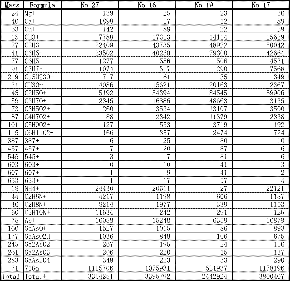
- TOF-SIMS analysis Using a TOF-SIMS device (TRIF II) manufactured by Physical Electronics, USA, 69 Ga + was irradiated as primary ions, and positively charged secondary ions were detected with a Time-of-Flight type mass spectrometer. The detected mass number range is 0.5 to 2000. However, in TOF-SIMS analysis, adhesion molecules were decomposed by irradiation with Ga + primary ions, and molecular species after decomposition were detected. Therefore, molecular species having a mass number of 1000 or more had a very small detection amount.
- the relative intensity of the cation (CH 3 O + ) signal having a mass number of 31 is 2.4 ⁇ 10 ⁇ 3 or more. understood. It was also found that the relative intensity of the cation (C 3 H 5 O 2 + ) signal having a mass number of 73 was 3.2 ⁇ 10 ⁇ 4 or more.
- the relative intensity of the signal of mass number 31 is 2. It was 0 times or more. Further, the relative intensity of the signal of mass number 73 was 4.1 times or more in the present invention as compared with the standard washed product.
- the “standard cleaning product” refers to a substrate cleaned in accordance with, for example, the steps shown as the conventional process in FIG. 3 (or, for example, standard cleaning shown in Example 1 described later).
- XPS analysis using synchrotron radiation as incident light was performed.
- the horizontal axis was calibrated with an incident X-ray energy of 365 eV, a photoelectron extraction angle of 90 degrees, and a C 1 s peak on the low energy side set to 285 eV, the standard cleaning product detected only the 285 eV peak.
- a peak was also detected on the high energy side of 1 to 2 eV.
- Nonionic surfactants representative of solutions containing organic substances containing hydrogen (H), carbon (C) and oxygen (O) used for surface treatment are polyoxyalkylene alkyl ethers having a molecular weight of 700 to 2000, polyoxyalkylene Examples include higher alcohols such as ethylene alkyl ether and polyoxyethylene alkyl phenyl ether, and alkylphenols.
- fatty acid-based surfactants can be used as nonionic surfactants.
- fatty acid surfactants include sucrose fatty acid salts / esters, sorbitan fatty acid esters, polyoxyethylene sorbitan fatty acid esters, polyoxyethylene fatty acid esters, and alkanolamides.
- the molecular weight of the nonionic surfactant is preferably 700 to 2000. If the molecular weight is small, the siloxane floating in the air has a large molecular weight, so that the possibility that the surfactant is replaced with the siloxane having a large molecular weight is increased. On the other hand, when the molecular weight increases, it becomes difficult to bond to the surface of the compound semiconductor substrate, so that it is difficult to form a film having a required thickness. Therefore, the molecular weight is optimally 800 to 2000.
- the pH of the surfactant solution is preferably weakly acidic. If the acidity is strong, particles tend to adhere to the surface during processing. Accordingly, the pH is preferably 2-7. Adjustment of pH can use inorganic acids, such as hydrochloric acid and nitric acid, or organic acids, such as a citric acid, malic acid, and an acetic acid.
- inorganic acids such as hydrochloric acid and nitric acid
- organic acids such as a citric acid, malic acid, and an acetic acid.
- the immersion time in the surfactant is not particularly limited as long as it is 10 seconds or longer, but it is economically disadvantageous if the time is long. If it is less than 10 seconds, the thickness of the surfactant layer to be formed is insufficient.
- the silicon (Si) peak concentration in the SIMS analysis of the interface between the epitaxial film obtained by growing the compound semiconductor substrate treated according to the present invention at a growth temperature of 550 ° C. without high temperature thermal cleaning before growth and the compound semiconductor substrate is 2 ⁇ 10 17 atoms / cm 3 or less.
- a GaAs substrate was prepared.
- the GaAs substrate is manufactured by the VB method (vertical boat method), the carbon doping amount is 1 ⁇ 10 15 to 2 ⁇ 10 16 / cm 3 , the oxygen in the crystal is 5 ⁇ 10 16 to 5 ⁇ 10 17 / cm 3 ,
- a substrate having a crystal defect EPD (Etch Pit Density) of 1000 / cm 2 or less and a specific resistance of 1 ⁇ 10 7 ⁇ cm to 6 ⁇ 10 8 ⁇ cm and having a diameter of 4 inches was prepared.
- the substrate surface orientation was a (100) 2 ° off substrate (surface orientation tolerance ⁇ 0.5 °) that is generally used for MOCVD epitaxial for electronic device applications.
- a substrate that has been turned off from (100) according to the conditions and device performance of MOCVD such as a (100) ⁇ 0.5 ° substrate or a (100) 0.05 ° to 2 ° off substrate.
- the treatment with the nonionic surfactant of the present invention can provide the same effect with any substrate.
- the crystal when the crystal is a polycrystal, impurities are concentrated along the grain boundary. If a device is formed on the crystal, a current may flow through the grain boundary. Therefore, the crystal needs to be a single crystal. . Further, if the specific resistance of the substrate is less than 1 ⁇ 10 7 ⁇ cm, when a voltage is applied, the current leaks to the substrate beyond the high-purity GaAs layer having a thickness of about 1 ⁇ m. Therefore, an epitaxial substrate for HEMT Then, the specific resistance of the substrate is also important, and 1 ⁇ 10 7 ⁇ cm or more is necessary.
- an n-type collector layer having a concentration of about 1 ⁇ 10 18 atoms / cm 3 is formed on a semi-insulating substrate. Even if it is about ⁇ 10 18 atoms / cm 3, there is no problem.
- non-ionic surfactant A having a molecular weight of 700 to 900 and a molecular weight of 800 to After immersing in a 0.1 to 3 vol% aqueous solution of 1200 nonionic surfactant B and nonionic surfactant C (polyoxyalkylene alkyl ether) having a molecular weight of 800 to 1000 for 5 to 120 seconds (treatment time), After rinsing with ultrapure water for a predetermined time (rinsing time (second)) as appropriate, spin drying was performed.
- the substrate soaked in the surfactant and the substrate not soaked were placed in a normal wafer tray and purged with nitrogen, and then placed in a clean bag that did not allow oxygen and moisture to pass through and sealed and stored. All storage methods and locations are the same.
- the wafer tray and bag used did not contain an organic Si compound (siloxane) (siloxane outgas amount ⁇ 0.01 ⁇ g / g).
- siloxane organic Si compound
- the standard cleaning performed here is a general cleaning method performed after the surface is polished into a mirror surface, and specifically, the following method was used.
- (1) Immerse in a 0.5 vol% aqueous solution of tetramethylammonium hydroxide at room temperature (25 ° C) for 5 minutes (2) Rinse with ultrapure water 3 minutes (3) Add a 0.5 vol% aqueous solution of tetramethylammonium hydroxide in room temperature (25 ° C ) 5 minutes immersion (4) Ultrapure water rinse 3 minutes (5) Immerse in pH 5 nitric acid aqueous solution at room temperature (25 ° C.) for 3 minutes (6) Ultrapure water rinse 3 minutes twice (7) Centrifugal spin dry Other commonly known cleaning methods can also be used.
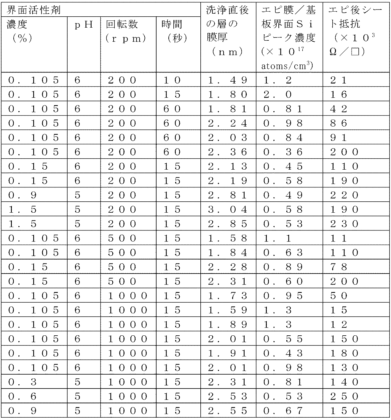
- the thickness of the surfactant layer was measured.
- the thickness of the surfactant layer can be measured with an ellipsometer (RUDOLPH AUTO ELIV).
- the ellipsometer parameters were fixed at a measurement light wavelength of 632.8 nm, a substrate refractive index of 3.857, a substrate attenuation factor of 0.217, and a surfactant layer refractive index of 1.8 for convenience of calculation.
- the surface of the substrate provided with a surfactant layer has a natural oxide film layer under the surfactant layer.
- This natural oxide film layer is about 0.7 nm, but with an ellipsometer, it is very difficult to measure and analyze the thickness of the thin natural oxide film and the thin surfactant layer on the ellipsometer.
- the thickness of the film (layer) in a state where both the natural oxide film and the surfactant layer are combined is calculated as “film thickness”.
- the thickness of the surfactant layer refers to the thickness of this natural oxide film.
- the sheet resistance of the substrate in which the thickness of the surfactant layer exceeds 1.50 nm is a high resistance of 10.0 ⁇ 10 3 ⁇ / ⁇ or more. It was.
- the sheet resistance of the conventional product that was not immersed in the surfactant was 5.6 ⁇ 10 3 ⁇ / ⁇ or less, and the resistance value decreased.
- the thickness of the surfactant layer exceeds 1.50 nm as a film thickness value.
- the peak concentration was 2.0 ⁇ 10 17 atoms / cm 3 or less and there was very little contamination.
- the thickness of the surfactant layer is less than 1.5 nm as the value of the film thickness, the amount of Si at the interface between the epitaxial film and the substrate is not significantly reduced compared to the conventional product, and the sheet resistance value is not so high. The effect of the surfactant layer is small.
- the film thickness is 1.5 nm or more, the sheet resistance value is sufficiently high, but if it exceeds 3.0 nm, the surface of the substrate before epitaxial growth is clouded white or the thick surfactant layer reaches the epitaxial growth temperature. During the heating, it became difficult to evaporate, and the surface of the epitaxial film was uneven.
- the thickness of the surfactant layer is preferably 1.5 nm or more and 3.0 nm or less as the value of the film thickness.
- the case of 1.5 nm to 2.0 nm is preferable because Si contamination is small and the possibility of contamination due to residual carbon and oxygen at the interface due to insufficient decomposition (transpiration) of the film during epitaxial growth is very small. .
- the thickness of the surfactant layer can be easily measured with an ellipsometer, and the amount of Si at the interface after epitaxial growth can be estimated from the thickness, so that the substrate quality can be more reliably controlled.
- the natural oxide film on the substrate surface immediately after cleaning is still in an unstable state and becomes a stable oxide film in about one week, during which the film thickness on the substrate surface is about 0.3 nm.
- the thickness of the substrate on which the surfactant layer is formed is increased by about 0.3 nm after being changed with time for one week as compared with the thickness immediately after the coating of the surfactant.
- the substrate surface was subjected to TOF-SIMS analysis using another substrate cleaned and stored in the same manner as 16, 17, 19, 20, 27, and 28. Two pieces of each substrate were analyzed.
- the product of the present invention has a large amount of organic substance containing H, C and O.
- the Si peak concentration on the surface is 2 ⁇ 10 17 or less when the relative intensity of the mass 31 signal is 2.4 ⁇ 10 ⁇ 3 or more.
- the relative intensity of the signal of mass number 73 is 3.2 ⁇ 10 ⁇ 4 or more.
- the Si peak concentration is 2 ⁇ 10 17 or less because the relative intensity of the signal of mass number 31 is 2.0 of the standard cleaning product (No. 27). It is a case of more than double. If the signal is mass 73, it is found to be 4.1 times or more. In the standard cleaning, since the surface is not coated with long chain C, there is no resistance to siloxane, and relative signal strengths such as mass numbers 31, 73, etc. in TOF-SIMS show almost the same low values. Siloxane varies, and the amount of interfacial Si changes sensitively.
- synchrotron radiation XPS analysis was performed using another substrate cleaned and stored in the same manner as Nos. 16, 17, and 27 (standard cleaning products).
- the beam source (BL12) of Kyushu Synchrotron Light Research Center was used as the light source, the incident X-ray energy was 365 eV, the pass energy was 11.75 eV, and the emission electron extraction angle was 90 °.
- the XPS spectra are collectively shown in FIG. It can be seen that the product of the present invention has a peak on the high energy side of 1 to 2 eV from the C1s peak of 285 eV. The lower the Si amount, the higher the peak on the high energy side. Comparing the integrated intensity of the peak at 285 eV and the integrated intensity of the peak on the high energy side from these spectra, the integrated intensity of the peak on the high energy side is 285 eV from FIG. 9 in order to make the Si peak concentration 2 ⁇ 10 17 or less. It can be seen that it may be 0.25 times or more of the integrated intensity of the peak.
- a GaAs substrate was prepared.
- the GaAs substrate is manufactured by the VGF method (vertical boat method), the carbon doping amount is 1 ⁇ 10 15 to 2 ⁇ 10 16 / cm 3 , the oxygen in the crystal is 5 ⁇ 10 15 to 5 ⁇ 10 16 / cm 3 ,
- a substrate having a crystal defect EPD (Etch Pit Density) of 500 / cm 2 or less and a specific resistance of 1 ⁇ 10 7 to 1 ⁇ 10 8 ⁇ cm and a diameter of 6 inches was prepared.
- the substrate surface orientation was a (100) 2 ° off substrate (surface orientation tolerance ⁇ 0.5 °).
- the surface When applying by the single wafer method, the surface is coated with an aqueous solution of a nonionic surfactant, but if it goes around the back side, it causes fogging of the back side, so the back side was washed with ultrapure water. Furthermore, in order to improve the drying property of the back surface during drying, nitrogen was sprayed from the back surface side to promote drying. Thereafter, the thickness of the surfactant layer was measured with an ellipsometer in the same manner as in Example 1.
- the sheet resistance is as high as 10 ⁇ 10 3 ⁇ / ⁇ or more, and the Si peak concentration at the interface is also 2 ⁇ 10 17 atoms. / Cm 3 or less.
- the film thickness of the surfactant layer immediately after cleaning was in the range of 1.5 nm to 3.0 nm with one significant digit.
- a GaAs substrate was prepared.
- the GaAs substrate is manufactured by the VGF method (vertical boat method) and is semi-insulating with a carbon doping amount of 1 ⁇ 10 15 to 2 ⁇ 10 16 / cm 3 and a specific resistance of 1 ⁇ 10 7 to 5 ⁇ 10 8 ⁇ cm.
- a substrate having a diameter of 6 inches was prepared.
- the substrate surface orientation was a (100) 2 ° off substrate (surface orientation tolerance ⁇ 0.3 °).
- Draining drying uses a solution obtained by further diluting an aqueous solution of 30 vol% nonionic surfactant (polyoxyethylene nonylphenyl ether) having a molecular weight of 800 to 1100 to 0.5%, and the upper atmosphere of the dryer is highly purified. Purge with nitrogen. After immersing the compound semiconductor substrate in a drying tank containing the aqueous solution for 2 minutes, the compound semiconductor substrate was slowly pulled up and dried at a constant rate. That is, at the time of pulling and drying, a film of a nonionic surfactant is formed on the surface of the compound semiconductor substrate, and the hydrophilic group (hydrogen bonding portion) of the nonionic surfactant is hydrogen bonded to the substrate surface.
- nonionic surfactant polyoxyethylene nonylphenyl ether
- the substrate surface is hydrophobic. For this reason, as soon as the substrate comes out of the aqueous solution into the nitrogen atmosphere, the water runs out of the substrate surface. If the substrate is slowly pulled up as it is, the surface of the substrate is dried while forming a surface active agent layer. Done.
- the thickness of the surfactant layer on the surface of the substrate thus treated was 2.0 nm as an ellipsometer film thickness.
- the film was taken out from the sealed bag and an epitaxial film was formed by MOCVD in the same manner as in Example 1. After forming the epitaxial film, the sheet resistance of the substrate was measured. As a result, the sheet resistance was as high as 9.9 ⁇ 10 4 ⁇ / ⁇ .
- the Si peak concentration at the interface was 1.1 ⁇ 10 17 atoms / cm 3 .
- a GaAs substrate was prepared.
- the GaAs substrate is manufactured by the VB method (vertical boat method), doped with carbon in the same manner as in Example 2, oxygen in the crystal is 1 ⁇ 10 16 to 1 ⁇ 10 17 / cm 3 , crystal defect EPD (Etch Pit A semi-insulating substrate having a density of 1000 / cm 2 or less and a specific resistance of 0.5 ⁇ 10 8 to 2.0 ⁇ 10 8 ⁇ cm and a 6-inch diameter substrate was prepared.
- the substrate surface orientation was a (100) 2 ° off substrate (surface orientation tolerance ⁇ 0.5 °).
- the GaAs substrate was cut into thin pieces from an ingot, chamfered on the outer periphery, and then double-side polished using a hard polishing cloth to mirror both sides. Further, the surface on which the element is manufactured is mirror-finished with a hard polishing cloth, finished to a surface roughness RMS of 0.10 nm and a flatness of TTV of 1.5 ⁇ m, and then batch cleaning with the same standard cleaning solution as in Example 1. The substrate was once dried.
- a 0.087 wt% aqueous solution of the surfactant C is applied to the surface of the GaAs substrate, and after 15 seconds of rotation at 1000 rpm, 35 seconds at a high speed of 2000 rpm. After drying, the thickness of the surfactant layer was measured with an ellipsometer in the same manner as in Example 1. At this time, the surfactant stock solution was purified and controlled to impurities of 50 ng / mm 3 or less for impurities other than C, H, and O.
- a single wafer rotation processing apparatus that holds the wafer (substrate) horizontally is used, and the Si concentration in the atmosphere in which the treatment is performed is controlled to be less than 0.5 ⁇ g / m 3 .
- an activated carbon filter for removing silicon-containing organic substances (siloxane) in the atmosphere is attached to the air conditioning system, and a ULPA filter made of fluororesin free from Si contamination is attached to the treatment chamber for coating, and the dust concentration Is less than 1 / ft 3 .
- the wafer (substrate) was supported by three polyimide resin pins on the outer periphery, and was arranged so that contamination from the outer periphery was minimized.
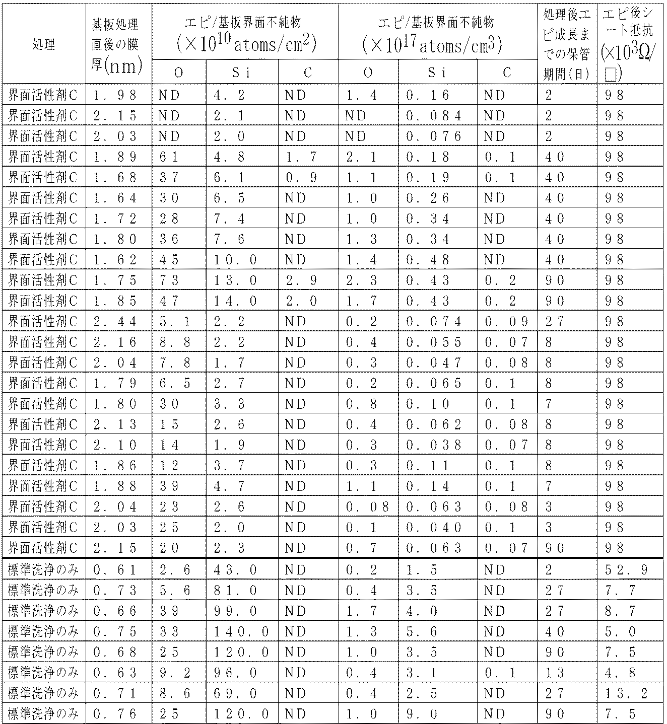
- the number of foreign substances having the film thicknesses shown in Table 5 and having an in-plane distribution of film thickness of less than ⁇ 0.3 nm and a diameter of 0.3 ⁇ m or more on the surface is 50 or less (the outer periphery is 3 mm, which is the edge part of the measuring instrument)
- the substrate with a film whose surface heavy metal analyzed by TXRF (total reflection fluorescent X-ray apparatus) was less than 10 ⁇ 10 10 atoms ⁇ cm 2 could be obtained.
- the standing time after standard cleaning is long, surface oxidation proceeds, and the surface state changes from a hydrophilic surface immediately after cleaning to a hydrophobic surface.
- the number of surface foreign matters was measured with Surfscan 6220 manufactured by Tencor. It is desirable that the amount of surface foreign matter is small because it becomes a defect after the formation of the epitaxial film. Since heavy metal on the surface is difficult to evaporate during heating before the formation of the epitaxial film, when the amount of heavy metal increases, leakage at the interface occurs. For this reason, it is desirable that the heavy metal is at least 50 ⁇ 10 10 atoms / cm 2 or less, preferably 10 ⁇ 10 10 atoms / cm 2 or less.
- an epitaxial film was formed by MOCVD as in Example 1, and the Si amount and sheet resistance at the interface between the epitaxial film and the substrate were measured.
- the results are shown in Table 5.
- the amount of Si at the interface increases and the sheet resistance tends to decrease, whereas when the surfactant treatment is added, the storage period becomes as long as 90 days.
- the amount of Si at the interface was kept low, and the sheet resistance was maintained at a high resistance exceeding the measurement limit of the measuring apparatus.
- the present invention since there is little adhesion of impurities including Si to the substrate surface, surface roughness that occurs when these impurities evaporate is suppressed, and deterioration of interface crystallinity and flatness is suppressed, thereby reducing device characteristics. It is thought that it is connected to improvement. Therefore, in the present invention, since the leakage current can be reduced even if the epitaxial film is formed by the low temperature cleaning, the merit of the cost reduction by shortening the production time and the consumption of the arsine which is the raw material gas consumed during the cleaning is reduced. Is big. From Table 5, it can be seen that in the present invention, the amounts of O and C are also low at the epi / substrate interface.
- n-type substrate When an n-type substrate is used to produce an element that allows current to flow from the epi surface to the back surface of the substrate, carrier reduction at the interface can be suppressed, and an increase in operating voltage can be suppressed. Further, when an electronic element is manufactured using a semi-insulating substrate, the back gate effect and the site gate effect can be suppressed, and high frequency characteristics can be improved. Thus, the effect of reducing other impurities can be expected in addition to the effect of reducing the amount of interface Si.
- the present invention it is possible to provide a semi-insulating compound semiconductor substrate that is less likely to cause an abnormality in electrical characteristics even when stored for a long period of time and can supply epitaxial growth for HEMT at a low cost.
Landscapes
- Cleaning Or Drying Semiconductors (AREA)
- Chemical Vapour Deposition (AREA)
- Crystals, And After-Treatments Of Crystals (AREA)
- Recrystallisation Techniques (AREA)
- Formation Of Insulating Films (AREA)
- Weting (AREA)
- Mechanical Treatment Of Semiconductor (AREA)
Abstract
Description
(1)テトラメチルアンモニウムハイドロオキシド0.5vol%水溶液に室温(25℃)で5分浸漬
(2)超純水リンス3分
(3)テトラメチルアンモニウムハイドロオキシド0.5vol%水溶液に室温(25℃)で5分浸漬
(4)超純水リンス3分
(5)pH5の硝酸酸性水溶液に室温(25℃)3分浸漬
(6)超純水リンス3分を2回
(7)遠心振り切り乾燥
但し、一般的に知られている他の洗浄方法を用いることもできる。


2 i-GaAs層(高純度エピタキシャル層)
3 n-AlGaAs層(電子供給層)
4 ソース電極
5 ゲート電極
6 ドレン電極
11 正常な電流の流れ
12 異常な電流の流れ
20 界面活性剤
21 有機汚染
Claims (11)
- 少なくとも1主面が鏡面研磨された化合物半導体基板であって、該鏡面研磨面が水素(H)、炭素(C)及び酸素(O)を含む有機物で被覆されたことを特徴とする化合物半導体基板。
- 前記有機物の分子量が700以上2000以下であることを特徴とする請求項1に記載の化合物半導体基板。
- 前記被覆された有機物のエリプソメータで測定した膜厚が、1.5nm以上3.0nm以下であることを特徴とする請求項1又は2に記載の化合物半導体基板。
- 前記有機物が非イオン系界面活性剤であることを特徴とする請求項1~3のいずれか1項に記載の化合物半導体基板。
- 一次イオンとして69Ga+を用いたTOF-SIMS分析により、質量数31の陽イオン(CH3O+)信号が相対強度で2.4×10⁻³以上を有することを特徴とする請求項1~4のいずれか1項に記載の化合物半導体基板。
- 一次イオンとして69Ga+を用いたTOF-SIMS分析により、質量数73の陽イオン(C3H5O2 +)信号が相対強度3.2×10⁻⁴以上を有することを特徴とする請求項1~4のいずれか1項に記載の化合物半導体基板。
- 一次イオンとして69Ga+を用いたTOF-SIMS分析により、質量数31の陽イオン(CH3O+)相対強度が、標準洗浄の化合物半導体基板の該相対強度の2.0倍以上であることを特徴とする請求項1~4のいずれか1項に記載の化合物半導体基板。
- 一次イオンとして69Ga+を用いたTOF-SIMS分析により、質量数73の陽イオン(C3H5O2 +)相対強度が、標準洗浄の化合物半導体基板の該相対強度の4.1倍以上であることを特徴とする請求項1~4のいずれか1項に記載の化合物半導体基板。
- 入射X線エネルギー365eV、取り出し角度90度の放射光XPS分析により、C1s:285eVのピークに対して1.5±0.5eV高エネルギー側にピークが検出されることを特徴とする請求項1~4のいずれか1項に記載の化合物半導体基板。
- 前記高エネルギー側のピークの積分強度が、前記285eV付近のピークの積分強度の0.25倍以上であることを特徴とする請求項9に記載の化合物半導体基板。
- 少なくとも1主面が鏡面加工された化合物半導体基板であって、成長温度550℃で成長させたエピタキシャル膜と前記化合物半導体基板との界面のシリコン(Si)ピーク濃度が、2×1017cm-3以下であることを特徴とする化合物半導体基板。
Priority Applications (3)
| Application Number | Priority Date | Filing Date | Title |
|---|---|---|---|
| CN201280014248.2A CN103460349B (zh) | 2011-05-18 | 2012-05-09 | 化合物半导体衬底 |
| DE112012002127.4T DE112012002127B4 (de) | 2011-05-18 | 2012-05-09 | Verfahren zur Herstellung eines Verbindungshalbleitersubstrats |
| JP2013515086A JP6070548B2 (ja) | 2011-05-18 | 2012-05-09 | 化合物半導体基板 |
Applications Claiming Priority (2)
| Application Number | Priority Date | Filing Date | Title |
|---|---|---|---|
| JP2011110980 | 2011-05-18 | ||
| JP2011-110980 | 2011-05-18 |
Publications (1)
| Publication Number | Publication Date |
|---|---|
| WO2012157476A1 true WO2012157476A1 (ja) | 2012-11-22 |
Family
ID=47174341
Family Applications (1)
| Application Number | Title | Priority Date | Filing Date |
|---|---|---|---|
| PCT/JP2012/061815 Ceased WO2012157476A1 (ja) | 2011-05-18 | 2012-05-09 | 化合物半導体基板 |
Country Status (6)
| Country | Link |
|---|---|
| US (1) | US9000567B2 (ja) |
| JP (5) | JP6070548B2 (ja) |
| CN (2) | CN103460349B (ja) |
| DE (3) | DE112012007376B4 (ja) |
| TW (3) | TWI588876B (ja) |
| WO (1) | WO2012157476A1 (ja) |
Cited By (2)
| Publication number | Priority date | Publication date | Assignee | Title |
|---|---|---|---|---|
| WO2018216440A1 (ja) * | 2017-05-26 | 2018-11-29 | 住友電気工業株式会社 | Iii-v族化合物半導体基板およびエピタキシャル層付iii-v族化合物半導体基板 |
| JP2019026526A (ja) * | 2017-08-01 | 2019-02-21 | 株式会社サイオクス | 半導体積層物の製造方法、窒化物半導体自立基板の製造方法、半導体積層物および半導体装置 |
Families Citing this family (12)
| Publication number | Priority date | Publication date | Assignee | Title |
|---|---|---|---|---|
| CN103460349B (zh) * | 2011-05-18 | 2016-11-23 | 住友电气工业株式会社 | 化合物半导体衬底 |
| JP6296001B2 (ja) | 2015-05-20 | 2018-03-20 | 信越半導体株式会社 | シリコンエピタキシャルウェーハの製造方法及び評価方法 |
| CN107958835A (zh) * | 2016-10-14 | 2018-04-24 | 上海新昇半导体科技有限公司 | 一种半导体晶圆的抛光方法 |
| CN107039244B (zh) * | 2017-04-14 | 2020-02-21 | 广东先导先进材料股份有限公司 | 半导体晶片的处理工艺 |
| US10822722B2 (en) * | 2017-07-04 | 2020-11-03 | Sumitomo Electric Industries, Ltd. | Gallium arsenide crystal body and gallium arsenide crystal substrate |
| JP6512369B1 (ja) * | 2017-09-21 | 2019-05-15 | 住友電気工業株式会社 | 半絶縁性化合物半導体基板および半絶縁性化合物半導体単結晶 |
| CN113584593B (zh) | 2017-09-21 | 2024-01-02 | 住友电气工业株式会社 | 半绝缘性砷化镓晶体基板 |
| JP6530125B1 (ja) * | 2018-04-27 | 2019-06-12 | 住友化学株式会社 | 光学フィルム |
| US12338546B2 (en) * | 2018-08-07 | 2025-06-24 | Sumitomo Electric Industries, Ltd. | Gallium arsenide single crystal and gallium arsenide single crystal substrate |
| WO2022070969A1 (ja) * | 2020-09-30 | 2022-04-07 | 株式会社フジミインコーポレーテッド | 酸化ガリウム基板用洗浄剤 |
| EP4589058A4 (en) * | 2022-09-16 | 2025-10-29 | Sumitomo Electric Industries | MONOCRYSTALLINE GALLIUM ARSENIIDE SUBSTRATE AND ITS PRODUCTION PROCESS |
| KR20250048914A (ko) * | 2023-10-04 | 2025-04-11 | 에스케이엔펄스 주식회사 | 반도체 공정용 연마 조성물 및 이를 이용한 기판의 연마방법 |
Citations (4)
| Publication number | Priority date | Publication date | Assignee | Title |
|---|---|---|---|---|
| JPH06151304A (ja) * | 1992-11-13 | 1994-05-31 | Toshiba Corp | 化合物半導体ウェーハ |
| JPH1012553A (ja) * | 1996-06-20 | 1998-01-16 | Hitachi Cable Ltd | 化合物半導体ウェハ及びその製造方法 |
| JP2001053011A (ja) * | 1999-06-02 | 2001-02-23 | Japan Energy Corp | 化合物半導体ウエーハ及びこれを用いた半導体デバイス |
| JP2007235036A (ja) * | 2006-03-03 | 2007-09-13 | Toshiba Ceramics Co Ltd | シリコンウエハの親水化処理方法及びそれに用いる親水化処理剤 |
Family Cites Families (23)
| Publication number | Priority date | Publication date | Assignee | Title |
|---|---|---|---|---|
| JPS60126838A (ja) | 1983-12-13 | 1985-07-06 | Mitsubishi Monsanto Chem Co | ひ化ガリウム単結晶ウエハの洗滌液および洗滌方法 |
| JP3502651B2 (ja) * | 1993-02-08 | 2004-03-02 | トリクイント セミコンダクター テキサス、エルピー | 電極形成法 |
| JPH07211688A (ja) | 1993-05-17 | 1995-08-11 | Japan Energy Corp | 化合物半導体基板の製造方法 |
| JP2861776B2 (ja) * | 1993-12-28 | 1999-02-24 | 日立電線株式会社 | 保護膜付き半導体ウェハ |
| JPH1079363A (ja) | 1996-09-03 | 1998-03-24 | Hitachi Cable Ltd | 化合物半導体ウエハの表面処理方法 |
| JPH11126766A (ja) * | 1997-10-24 | 1999-05-11 | Hitachi Cable Ltd | 半導体結晶ウエハの洗浄方法 |
| JP3456446B2 (ja) | 1999-05-28 | 2003-10-14 | 日立電線株式会社 | 半導体結晶ウエハの洗浄方法 |
| JP3449474B2 (ja) * | 2000-02-03 | 2003-09-22 | 日本電気株式会社 | 半導体基板の表面処理用組成物および表面処理方法 |
| WO2001071789A1 (fr) * | 2000-03-21 | 2001-09-27 | Wako Pure Chemical Industries, Ltd. | Agent de nettoyage de tranche de semi-conducteur et procede de nettoyage |
| JP3498288B2 (ja) * | 2001-01-16 | 2004-02-16 | 株式会社スーパーシリコン研究所 | 半導体ウエハ研磨方法 |
| JP2003100671A (ja) * | 2001-09-20 | 2003-04-04 | Hitachi Cable Ltd | 半導体結晶ウェハの研磨方法及び半導体結晶ウェハ |
| JP2003109930A (ja) * | 2001-09-28 | 2003-04-11 | Mitsubishi Chemicals Corp | 半導体デバイス用基板の洗浄液及び洗浄方法 |
| JP2004193407A (ja) * | 2002-12-12 | 2004-07-08 | Hitachi Cable Ltd | 化合物半導体ウエハの洗浄方法 |
| JP4350364B2 (ja) * | 2002-12-12 | 2009-10-21 | 昭和電工株式会社 | 洗浄剤組成物、半導体ウェーハの洗浄方法および製造方法 |
| CN100428419C (zh) * | 2004-12-08 | 2008-10-22 | 中国电子科技集团公司第四十六研究所 | 一种砷化镓晶片清洗方法 |
| JP4872246B2 (ja) * | 2005-06-10 | 2012-02-08 | 住友電気工業株式会社 | 半絶縁性GaAs基板及びエピタキシャル基板 |
| CN1933096B (zh) * | 2005-09-14 | 2010-04-21 | 中国科学院半导体研究所 | 一种低温晶片直接键合方法 |
| JP5276281B2 (ja) * | 2007-06-01 | 2013-08-28 | 住友電気工業株式会社 | GaAs半導体基板およびその製造方法 |
| CN101965542B (zh) * | 2008-03-10 | 2013-03-27 | 旭化成电子材料株式会社 | 感光性聚有机硅氧烷组合物 |
| JP5471001B2 (ja) * | 2009-04-20 | 2014-04-16 | 住友電気工業株式会社 | インジウムリン基板の製造方法、エピタキシャルウエハの製造方法、インジウムリン基板およびエピタキシャルウエハ |
| JP5635246B2 (ja) * | 2009-07-15 | 2014-12-03 | 住友電気工業株式会社 | Iii族窒化物半導体光素子及びエピタキシャル基板 |
| JP4513927B1 (ja) * | 2009-09-30 | 2010-07-28 | 住友電気工業株式会社 | Iii族窒化物半導体基板、エピタキシャル基板及び半導体デバイス |
| CN103460349B (zh) * | 2011-05-18 | 2016-11-23 | 住友电气工业株式会社 | 化合物半导体衬底 |
-
2012
- 2012-05-09 CN CN201280014248.2A patent/CN103460349B/zh active Active
- 2012-05-09 DE DE112012007376.2T patent/DE112012007376B4/de active Active
- 2012-05-09 WO PCT/JP2012/061815 patent/WO2012157476A1/ja not_active Ceased
- 2012-05-09 DE DE202012013658.5U patent/DE202012013658U1/de not_active Expired - Lifetime
- 2012-05-09 JP JP2013515086A patent/JP6070548B2/ja active Active
- 2012-05-09 DE DE112012002127.4T patent/DE112012002127B4/de active Active
- 2012-05-09 CN CN201611005643.0A patent/CN107039516B/zh active Active
- 2012-05-16 TW TW105127772A patent/TWI588876B/zh active
- 2012-05-16 US US13/473,043 patent/US9000567B2/en active Active
- 2012-05-16 TW TW106115883A patent/TWI625768B/zh active
- 2012-05-16 TW TW101117472A patent/TWI556288B/zh active
-
2016
- 2016-07-28 JP JP2016148028A patent/JP2016195278A/ja active Pending
-
2017
- 2017-06-09 JP JP2017113992A patent/JP2017152748A/ja active Pending
-
2019
- 2019-04-24 JP JP2019082594A patent/JP2019117959A/ja active Pending
-
2020
- 2020-11-06 JP JP2020185610A patent/JP7060060B2/ja active Active
Patent Citations (4)
| Publication number | Priority date | Publication date | Assignee | Title |
|---|---|---|---|---|
| JPH06151304A (ja) * | 1992-11-13 | 1994-05-31 | Toshiba Corp | 化合物半導体ウェーハ |
| JPH1012553A (ja) * | 1996-06-20 | 1998-01-16 | Hitachi Cable Ltd | 化合物半導体ウェハ及びその製造方法 |
| JP2001053011A (ja) * | 1999-06-02 | 2001-02-23 | Japan Energy Corp | 化合物半導体ウエーハ及びこれを用いた半導体デバイス |
| JP2007235036A (ja) * | 2006-03-03 | 2007-09-13 | Toshiba Ceramics Co Ltd | シリコンウエハの親水化処理方法及びそれに用いる親水化処理剤 |
Cited By (6)
| Publication number | Priority date | Publication date | Assignee | Title |
|---|---|---|---|---|
| WO2018216440A1 (ja) * | 2017-05-26 | 2018-11-29 | 住友電気工業株式会社 | Iii-v族化合物半導体基板およびエピタキシャル層付iii-v族化合物半導体基板 |
| JP6477990B1 (ja) * | 2017-05-26 | 2019-03-06 | 住友電気工業株式会社 | Iii−v族化合物半導体基板およびエピタキシャル層付iii−v族化合物半導体基板 |
| US10964786B2 (en) | 2017-05-26 | 2021-03-30 | Sumitomo Electric Industries, Ltd. | Group III-V compound semiconductor substrate and group III-V compound semiconductor substrate with epitaxial layer |
| US11444161B2 (en) | 2017-05-26 | 2022-09-13 | Sumitomo Electric Industries, Ltd. | Group III-V compound semiconductor substrate and group III-V compound semiconductor substrate with epitaxial layer |
| EP4660353A2 (en) | 2017-05-26 | 2025-12-10 | Sumitomo Electric Industries, Ltd. | Group iii-v compound semiconductor substrate and group iii-v compound semiconductor substrate with epitaxial layer |
| JP2019026526A (ja) * | 2017-08-01 | 2019-02-21 | 株式会社サイオクス | 半導体積層物の製造方法、窒化物半導体自立基板の製造方法、半導体積層物および半導体装置 |
Also Published As
| Publication number | Publication date |
|---|---|
| TW201705220A (zh) | 2017-02-01 |
| JP2016195278A (ja) | 2016-11-17 |
| DE202012013658U1 (de) | 2019-06-06 |
| US20120292747A1 (en) | 2012-11-22 |
| JP2017152748A (ja) | 2017-08-31 |
| TWI625768B (zh) | 2018-06-01 |
| CN103460349A (zh) | 2013-12-18 |
| CN103460349B (zh) | 2016-11-23 |
| JPWO2012157476A1 (ja) | 2014-07-31 |
| CN107039516A (zh) | 2017-08-11 |
| TWI588876B (zh) | 2017-06-21 |
| JP2021015999A (ja) | 2021-02-12 |
| CN107039516B (zh) | 2020-07-10 |
| TW201729258A (zh) | 2017-08-16 |
| DE112012002127T5 (de) | 2014-02-13 |
| DE112012002127B4 (de) | 2022-10-27 |
| JP7060060B2 (ja) | 2022-04-26 |
| US9000567B2 (en) | 2015-04-07 |
| TWI556288B (zh) | 2016-11-01 |
| JP6070548B2 (ja) | 2017-02-01 |
| JP2019117959A (ja) | 2019-07-18 |
| TW201250794A (en) | 2012-12-16 |
| DE112012007376B4 (de) | 2026-07-02 |
Similar Documents
| Publication | Publication Date | Title |
|---|---|---|
| JP7060060B2 (ja) | エピタキシャル成長用の化合物半導体基板の製造方法、化合物半導体基板上のエピタキシャル成長方法および化合物半導体基板 | |
| JP5471001B2 (ja) | インジウムリン基板の製造方法、エピタキシャルウエハの製造方法、インジウムリン基板およびエピタキシャルウエハ | |
| EP3514266B1 (en) | Group iii v compound semiconductor substrate and group iii v compound semiconductor substrate with epitaxial layer | |
| JP2008300747A (ja) | GaAs半導体基板およびその製造方法 | |
| TWI916629B (zh) | Iii-v族化合物半導體單晶基板及其製造方法 |
Legal Events
| Date | Code | Title | Description |
|---|---|---|---|
| 121 | Ep: the epo has been informed by wipo that ep was designated in this application |
Ref document number: 12785856 Country of ref document: EP Kind code of ref document: A1 |
|
| ENP | Entry into the national phase |
Ref document number: 2013515086 Country of ref document: JP Kind code of ref document: A |
|
| WWE | Wipo information: entry into national phase |
Ref document number: 112012002127 Country of ref document: DE Ref document number: 1120120021274 Country of ref document: DE |
|
| 122 | Ep: pct application non-entry in european phase |
Ref document number: 12785856 Country of ref document: EP Kind code of ref document: A1 |