WO2012157436A1 - セラミック電子部品およびその製造方法 - Google Patents
セラミック電子部品およびその製造方法 Download PDFInfo
- Publication number
- WO2012157436A1 WO2012157436A1 PCT/JP2012/061364 JP2012061364W WO2012157436A1 WO 2012157436 A1 WO2012157436 A1 WO 2012157436A1 JP 2012061364 W JP2012061364 W JP 2012061364W WO 2012157436 A1 WO2012157436 A1 WO 2012157436A1
- Authority
- WO
- WIPO (PCT)
- Prior art keywords
- external terminal
- terminal electrode
- forming
- electronic component
- ceramic
- Prior art date
- Legal status (The legal status is an assumption and is not a legal conclusion. Google has not performed a legal analysis and makes no representation as to the accuracy of the status listed.)
- Ceased
Links
Images




Classifications
-
- H—ELECTRICITY
- H05—ELECTRIC TECHNIQUES NOT OTHERWISE PROVIDED FOR
- H05K—PRINTED CIRCUITS; CASINGS OR CONSTRUCTIONAL DETAILS OF ELECTRIC APPARATUS; MANUFACTURE OF ASSEMBLAGES OF ELECTRICAL COMPONENTS
- H05K3/00—Apparatus or processes for manufacturing printed circuits
- H05K3/0091—Apparatus for coating printed circuits using liquid non-metallic coating compositions
-
- H—ELECTRICITY
- H05—ELECTRIC TECHNIQUES NOT OTHERWISE PROVIDED FOR
- H05K—PRINTED CIRCUITS; CASINGS OR CONSTRUCTIONAL DETAILS OF ELECTRIC APPARATUS; MANUFACTURE OF ASSEMBLAGES OF ELECTRICAL COMPONENTS
- H05K3/00—Apparatus or processes for manufacturing printed circuits
- H05K3/40—Forming printed elements for providing electric connections to or between printed circuits
- H05K3/4007—Surface contacts, e.g. bumps
-
- H—ELECTRICITY
- H10—SEMICONDUCTOR DEVICES; ELECTRIC SOLID-STATE DEVICES NOT OTHERWISE PROVIDED FOR
- H10W—GENERIC PACKAGES, INTERCONNECTIONS, CONNECTORS OR OTHER CONSTRUCTIONAL DETAILS OF DEVICES COVERED BY CLASS H10
- H10W70/00—Package substrates; Interposers; Redistribution layers [RDL]
- H10W70/01—Manufacture or treatment
- H10W70/05—Manufacture or treatment of insulating or insulated package substrates, or of interposers, or of redistribution layers
- H10W70/093—Connecting or disconnecting other interconnections thereto or therefrom, e.g. connecting bond wires or bumps
-
- H—ELECTRICITY
- H10—SEMICONDUCTOR DEVICES; ELECTRIC SOLID-STATE DEVICES NOT OTHERWISE PROVIDED FOR
- H10W—GENERIC PACKAGES, INTERCONNECTIONS, CONNECTORS OR OTHER CONSTRUCTIONAL DETAILS OF DEVICES COVERED BY CLASS H10
- H10W70/00—Package substrates; Interposers; Redistribution layers [RDL]
- H10W70/60—Insulating or insulated package substrates; Interposers; Redistribution layers
- H10W70/67—Insulating or insulated package substrates; Interposers; Redistribution layers characterised by their insulating layers or insulating parts
- H10W70/68—Shapes or dispositions thereof
- H10W70/685—Shapes or dispositions thereof comprising multiple insulating layers
-
- H—ELECTRICITY
- H10—SEMICONDUCTOR DEVICES; ELECTRIC SOLID-STATE DEVICES NOT OTHERWISE PROVIDED FOR
- H10W—GENERIC PACKAGES, INTERCONNECTIONS, CONNECTORS OR OTHER CONSTRUCTIONAL DETAILS OF DEVICES COVERED BY CLASS H10
- H10W70/00—Package substrates; Interposers; Redistribution layers [RDL]
- H10W70/60—Insulating or insulated package substrates; Interposers; Redistribution layers
- H10W70/67—Insulating or insulated package substrates; Interposers; Redistribution layers characterised by their insulating layers or insulating parts
- H10W70/69—Insulating materials thereof
- H10W70/692—Ceramics or glasses
-
- H—ELECTRICITY
- H10—SEMICONDUCTOR DEVICES; ELECTRIC SOLID-STATE DEVICES NOT OTHERWISE PROVIDED FOR
- H10W—GENERIC PACKAGES, INTERCONNECTIONS, CONNECTORS OR OTHER CONSTRUCTIONAL DETAILS OF DEVICES COVERED BY CLASS H10
- H10W90/00—Package configurations
- H10W90/701—Package configurations characterised by the relative positions of pads or connectors relative to package parts
-
- H—ELECTRICITY
- H05—ELECTRIC TECHNIQUES NOT OTHERWISE PROVIDED FOR
- H05K—PRINTED CIRCUITS; CASINGS OR CONSTRUCTIONAL DETAILS OF ELECTRIC APPARATUS; MANUFACTURE OF ASSEMBLAGES OF ELECTRICAL COMPONENTS
- H05K1/00—Printed circuits
- H05K1/02—Details
- H05K1/11—Printed elements for providing electric connections to or between printed circuits
- H05K1/111—Pads for surface mounting, e.g. lay-out
-
- H—ELECTRICITY
- H05—ELECTRIC TECHNIQUES NOT OTHERWISE PROVIDED FOR
- H05K—PRINTED CIRCUITS; CASINGS OR CONSTRUCTIONAL DETAILS OF ELECTRIC APPARATUS; MANUFACTURE OF ASSEMBLAGES OF ELECTRICAL COMPONENTS
- H05K2203/00—Indexing scheme relating to apparatus or processes for manufacturing printed circuits covered by H05K3/00
- H05K2203/02—Details related to mechanical or acoustic processing, e.g. drilling, punching, cutting, using ultrasound
- H05K2203/0278—Flat pressure, e.g. for connecting terminals with anisotropic conductive adhesive
-
- H—ELECTRICITY
- H05—ELECTRIC TECHNIQUES NOT OTHERWISE PROVIDED FOR
- H05K—PRINTED CIRCUITS; CASINGS OR CONSTRUCTIONAL DETAILS OF ELECTRIC APPARATUS; MANUFACTURE OF ASSEMBLAGES OF ELECTRICAL COMPONENTS
- H05K2203/00—Indexing scheme relating to apparatus or processes for manufacturing printed circuits covered by H05K3/00
- H05K2203/05—Patterning and lithography; Masks; Details of resist
- H05K2203/0502—Patterning and lithography
- H05K2203/0545—Pattern for applying drops or paste; Applying a pattern made of drops or paste
-
- H—ELECTRICITY
- H05—ELECTRIC TECHNIQUES NOT OTHERWISE PROVIDED FOR
- H05K—PRINTED CIRCUITS; CASINGS OR CONSTRUCTIONAL DETAILS OF ELECTRIC APPARATUS; MANUFACTURE OF ASSEMBLAGES OF ELECTRICAL COMPONENTS
- H05K2203/00—Indexing scheme relating to apparatus or processes for manufacturing printed circuits covered by H05K3/00
- H05K2203/14—Related to the order of processing steps
- H05K2203/1476—Same or similar kind of process performed in phases, e.g. coarse patterning followed by fine patterning
-
- H—ELECTRICITY
- H05—ELECTRIC TECHNIQUES NOT OTHERWISE PROVIDED FOR
- H05K—PRINTED CIRCUITS; CASINGS OR CONSTRUCTIONAL DETAILS OF ELECTRIC APPARATUS; MANUFACTURE OF ASSEMBLAGES OF ELECTRICAL COMPONENTS
- H05K3/00—Apparatus or processes for manufacturing printed circuits
- H05K3/10—Apparatus or processes for manufacturing printed circuits in which conductive material is applied to the insulating support in such a manner as to form the desired conductive pattern
- H05K3/12—Apparatus or processes for manufacturing printed circuits in which conductive material is applied to the insulating support in such a manner as to form the desired conductive pattern using thick film techniques, e.g. printing techniques to apply the conductive material or similar techniques for applying conductive paste or ink patterns
- H05K3/1216—Apparatus or processes for manufacturing printed circuits in which conductive material is applied to the insulating support in such a manner as to form the desired conductive pattern using thick film techniques, e.g. printing techniques to apply the conductive material or similar techniques for applying conductive paste or ink patterns by screen printing or stencil printing
-
- H—ELECTRICITY
- H05—ELECTRIC TECHNIQUES NOT OTHERWISE PROVIDED FOR
- H05K—PRINTED CIRCUITS; CASINGS OR CONSTRUCTIONAL DETAILS OF ELECTRIC APPARATUS; MANUFACTURE OF ASSEMBLAGES OF ELECTRICAL COMPONENTS
- H05K3/00—Apparatus or processes for manufacturing printed circuits
- H05K3/22—Secondary treatment of printed circuits
- H05K3/24—Reinforcing of the conductive pattern
- H05K3/245—Reinforcing conductive patterns made by printing techniques or by other techniques for applying conductive pastes, inks or powders; Reinforcing other conductive patterns by such techniques
- H05K3/246—Reinforcing conductive paste, ink or powder patterns by other methods, e.g. by plating
-
- H—ELECTRICITY
- H05—ELECTRIC TECHNIQUES NOT OTHERWISE PROVIDED FOR
- H05K—PRINTED CIRCUITS; CASINGS OR CONSTRUCTIONAL DETAILS OF ELECTRIC APPARATUS; MANUFACTURE OF ASSEMBLAGES OF ELECTRICAL COMPONENTS
- H05K3/00—Apparatus or processes for manufacturing printed circuits
- H05K3/38—Improvement of the adhesion between the insulating substrate and the metal
-
- H—ELECTRICITY
- H05—ELECTRIC TECHNIQUES NOT OTHERWISE PROVIDED FOR
- H05K—PRINTED CIRCUITS; CASINGS OR CONSTRUCTIONAL DETAILS OF ELECTRIC APPARATUS; MANUFACTURE OF ASSEMBLAGES OF ELECTRICAL COMPONENTS
- H05K3/00—Apparatus or processes for manufacturing printed circuits
- H05K3/46—Manufacturing multilayer circuits
- H05K3/4611—Manufacturing multilayer circuits by laminating two or more circuit boards
- H05K3/4626—Manufacturing multilayer circuits by laminating two or more circuit boards characterised by the insulating layers or materials
- H05K3/4629—Manufacturing multilayer circuits by laminating two or more circuit boards characterised by the insulating layers or materials laminating inorganic sheets comprising printed circuits, e.g. green ceramic sheets
-
- H—ELECTRICITY
- H10—SEMICONDUCTOR DEVICES; ELECTRIC SOLID-STATE DEVICES NOT OTHERWISE PROVIDED FOR
- H10W—GENERIC PACKAGES, INTERCONNECTIONS, CONNECTORS OR OTHER CONSTRUCTIONAL DETAILS OF DEVICES COVERED BY CLASS H10
- H10W70/00—Package substrates; Interposers; Redistribution layers [RDL]
- H10W70/60—Insulating or insulated package substrates; Interposers; Redistribution layers
- H10W70/62—Insulating or insulated package substrates; Interposers; Redistribution layers characterised by their interconnections
- H10W70/63—Vias, e.g. via plugs
- H10W70/635—Through-vias
-
- Y—GENERAL TAGGING OF NEW TECHNOLOGICAL DEVELOPMENTS; GENERAL TAGGING OF CROSS-SECTIONAL TECHNOLOGIES SPANNING OVER SEVERAL SECTIONS OF THE IPC; TECHNICAL SUBJECTS COVERED BY FORMER USPC CROSS-REFERENCE ART COLLECTIONS [XRACs] AND DIGESTS
- Y10—TECHNICAL SUBJECTS COVERED BY FORMER USPC
- Y10T—TECHNICAL SUBJECTS COVERED BY FORMER US CLASSIFICATION
- Y10T428/00—Stock material or miscellaneous articles
- Y10T428/24—Structurally defined web or sheet [e.g., overall dimension, etc.]
- Y10T428/24479—Structurally defined web or sheet [e.g., overall dimension, etc.] including variation in thickness
- Y10T428/24488—Differential nonuniformity at margin
Definitions
- the multilayer ceramic substrate is mounted on a predetermined mounting substrate, and the multilayer ceramic substrate is provided with external terminal electrodes that are electrically connected to the mounting substrate.
- the external terminal electrode of the multilayer ceramic substrate is usually printed on the ceramic green sheet placed on the outermost layer by screen printing, and the outermost ceramic green sheet is laminated together with other ceramic green sheets. Then, it is formed by firing. Further, the external terminal electrode after firing may be subjected to nickel plating and gold plating or nickel plating and tin plating as necessary.
- multilayer ceramic electronic components such as a multilayer ceramic substrate, but include, for example, a component main body made of a single-layer ceramic substrate, and external terminal electrodes along the main surface of the component main body. It can also be encountered in ceramic electronic components with a non-stacked structure provided with
- an object of the present invention is to provide a ceramic electronic component in which the bonding strength of the external terminal electrode is increased and a method for manufacturing the same.
- the surface of the external terminal electrode and the main surface of the component body are located on the same plane.
- a plating film may be formed on the surface of the external terminal electrode.
- the plating film is formed, there may be a problem that the plating solution penetrates from the interface between the external terminal electrode and the component body.
- the external terminal electrode is formed by the peripheral portion and the peripheral portion.
- the peripheral portion is thicker than the central portion, and at least a part of the peripheral portion is embedded in the component main body, thereby causing infiltration of the plating solution. Therefore, it is possible to make it difficult for the bonding strength of the external terminal electrode to decrease due to the penetration of the plating solution.
- the central portion and the peripheral portion of the external terminal electrode may have different compositions.
- the present invention may be directed to a multilayer ceramic electronic component.
- the component body includes a plurality of laminated ceramic layers, and further includes an internal conductor disposed inside the component body.
- the present invention is also directed to a method for manufacturing a ceramic electronic component.
- the manufacturing method according to the present invention includes a step of preparing a ceramic green sheet, a step of forming an external terminal electrode using a conductive paste on the main surface of the ceramic green sheet, and a ceramic green sheet on which the external terminal electrode is formed.
- the peripheral portion is thicker than the central portion surrounded by the peripheral portion.
- An external terminal electrode is formed. According to this manufacturing method, a ceramic electronic component having high bonding strength of the external terminal electrode can be manufactured.
- the peripheral portion and the central portion are formed separately.
- the phenomenon that the conductive paste collects in the central portion due to surface tension is suppressed, and therefore the thickness of the peripheral portion can be easily increased.
- problems such as a decrease in printability, a decrease in productivity, and an increase in manufacturing cost, which can be caused in the case of overcoating described above, can be advantageously avoided.
- the step of forming the peripheral portion is conversely performed after the step of forming the central portion. Also good.
- the step of forming the central portion is performed after the step of forming the peripheral portion as in the former, when the peripheral portion is printed by screen printing, the adhesion between the screen plate and the ceramic green sheet depends on the central portion. Since it is not hindered, good printability can be obtained.
- the step of forming the peripheral portion is performed after the step of forming the central portion as in the latter, it is easy to form the central portion thinner.
- the composition of the conductive paste used in the step of forming the peripheral portion and the composition of the conductive paste used in the step of forming the central portion can be made different from each other.
- the conductive paste used in the step of forming the peripheral portion has a higher content of inorganic material or the step of forming the peripheral portion than the conductive paste used in the step of forming the central portion.
- the amount of the organic solvent in the conductive paste used is smaller than that in the conductive paste used in the step of forming the central portion.
- the conductive paste used in the step of forming the peripheral portion has a higher inorganic material content than the conductive paste used in the step of forming the central portion, as in the former case, firing is performed. Accordingly, the inorganic material is firmly bonded to the glass component contained in the ceramic in the ceramic green sheet, and thus the bonding strength particularly at the peripheral portion can be improved. On the other hand, the more inorganic material is added to the conductive paste, the less dense the conductor film obtained by sintering, and the more likely moisture will enter from the outside.
- the conductive paste for forming the central portion when the content of the inorganic material is relatively reduced, a dense conductor film is formed in the central portion. In particular, since the central portion is formed relatively thin and may be connected to the via conductor inside the component main body, it is preferably a dense conductor film.
- the conductive paste used in the step of forming the peripheral portion as in the latter case described above, It becomes easier to print thicker, and it becomes easier to print the central portion thinner, which is more suitable for the purpose of the present invention.
- a step of pressing the ceramic green sheet on which the external terminal electrode is formed is performed before the above-described firing step.
- the peripheral edge of the external terminal electrode is embedded in the ceramic green sheet, and more preferably, the surface of the external terminal electrode is located on the same plane as the main surface of the ceramic green sheet. To be done.
- an electrically insulating coating layer on the ceramic green sheet so as to cover at least a part of the peripheral edge of the external terminal electrode.
- This covering layer is preferably formed by applying an insulating paste by screen printing.
- the peripheral portion is formed with good printability as described above. Therefore, it is possible to make it difficult for bleeding to occur during screen printing of the coating layer.
- the central portion can be formed thinner as described above, and therefore thicker. It is easy to increase the difference in thickness between the peripheral portion and the thinner central portion, and the adhesion between the screen plate for printing the coating layer and the peripheral portion can be improved, so screen printing of the coating layer Time blur can be made difficult to occur.
- the external terminal A step of pressing the ceramic green sheet on which the external terminal electrode and the coating layer are formed is performed so that the surface of the electrode and the surface of the coating layer are located on the same plane.
- the method for manufacturing a ceramic electronic component according to the present invention may further include a step of forming a plating film on the surface of the external terminal electrode.
- the manufacturing method according to the present invention is directed to a method for manufacturing a multilayer ceramic electronic component, a plurality of ceramic green sheets are prepared, and external terminal electrodes are formed on a specific one of the plurality of ceramic green sheets And a step of forming an inner conductor on a specific one of the plurality of ceramic green sheets, and a plurality of ceramic green sheets are laminated so that the external terminal electrode is positioned on one main surface. And the step of performing.
- the bonding strength of the external terminal electrode can be improved.
- the plating film is formed on the external terminal electrode, it is possible to make it difficult for the plating solution to enter from the interface between the external terminal electrode and the component main body. It is possible to make it difficult for the strength to decrease.
- the conductive paste usually contains a sintering inhibitor such as alumina in order to increase the bonding strength with the ceramic.
- a sintering inhibitor such as alumina
- the thickness is increased only at the peripheral portion that has a greater influence on the bonding strength of the external terminal electrode, and the thickness is suppressed at the central portion. Undesirable deformation such as warpage and undulation in the component main body due to the difference in the shrinkage behavior can be made difficult to occur.
- the effects of improving the bonding strength and suppressing the penetration of the plating solution can be further enhanced.
- the external terminal electrode is formed so that the thickness of the peripheral portion is thicker than the thickness of the central portion surrounded by the peripheral portion.
- a ceramic electronic component having high strength can be manufactured.
- FIG. 2 is a plan view for explaining a first embodiment of a method for forming an external terminal electrode 7 included in the ceramic electronic component 1 shown in FIG. (B) is sectional drawing which shows the state in which the peripheral part 8 was formed with the screen plate 22.
- FIG. 2A and 2B are diagrams for explaining a process performed subsequent to the process shown in FIG. 2, in which FIG. 3A is a plan view showing a state in which a central portion 9 is formed, and FIG. FIG. FIG. FIG. 4 is a cross-sectional view for explaining a process performed subsequent to the process shown in FIG. 3 and showing a state where a coating layer 11 is formed together with a screen plate 28.
- FIG. 2 is a plan view for explaining a first embodiment of a method for forming an external terminal electrode 7 included in the ceramic electronic component 1 shown in FIG. (B) is sectional drawing which shows the state in which the peripheral part 8 was formed with the screen plate 22.
- FIG. 2A and 2B are diagrams for explaining a process performed subsequent to the process
- FIG. 4 is a cross-sectional view showing a state after laminating and pressing the ceramic green sheet 21 on which the external terminal electrode 7 and the coating layer 11 are formed, for explaining a process performed subsequent to the process shown in FIG. It is.
- FIG. 6 is a cross-sectional view for explaining a process performed subsequent to the process shown in FIG. 5 and showing a state in which a plating film 13 is formed on the external terminal electrode 7 after the firing process.
- FIG. 2 is a plan view for explaining a second embodiment of a method for forming an external terminal electrode 7 provided in the ceramic electronic component 1 shown in FIG. 1, wherein (A) is a state in which a central portion 9 is formed. (B) is sectional drawing which shows the state in which the center part 9 was formed with the screen plate 35.
- FIG. 8 is a plan view showing a state in which the peripheral edge portion 8 is formed, and (B) is a state in which the peripheral edge portion 8 is formed.
- FIG. It is sectional drawing which shows the 1st modification of the formation state of an external terminal electrode. It is sectional drawing which shows the 2nd modification of the formation state of an external terminal electrode.
- FIG. 4 is a cross-sectional view for explaining a third embodiment of a method for forming an external terminal electrode 7 included in the ceramic electronic component 1 shown in FIG. 1 and showing the formed external terminal electrode 7 together with a screen plate 41. .
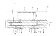
- the ceramic electronic component 1 constitutes a multilayer ceramic substrate, and includes a component body 3 having a laminated structure constituted by a plurality of laminated ceramic layers 2. Inside the component main body 3, several internal conductor films 4 are provided as internal conductors along a specific interface between the ceramic layers 2, and some via conductors 5 penetrate the specific ceramic layer 2. It is provided to do.
- the ceramic electronic component 1 also includes several external terminal electrodes 7 provided along the main surface 6 of the component main body 3.
- the ceramic electronic component 1 is mounted on the mounting substrate while the external terminal electrodes 7 are electrically connected to a mounting substrate (not shown) and mechanically fixed.
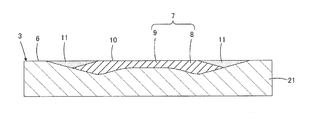
- the external terminal electrode 7 is shown enlarged in FIG. 6 shows the external terminal electrode 7 upside down as compared with FIG. As shown well in FIG. 6, the external terminal electrode 7 includes a peripheral portion 8 and a central portion 9 surrounded by the peripheral portion 8, and the peripheral portion 8 is thicker than the central portion 9.
- the peripheral edge 8 is embedded in the component main body 3.
- the surface 10 of the external terminal electrode 7 and the main surface 6 of the component main body 3 are located on the same plane.
- the ceramic electronic component 1 has the following characteristics in relation to the external terminal electrode 7 shown in FIG.
- An electrically insulating coating layer 11 is formed along the main surface 6 of the component body 3 so as to cover at least a part of the peripheral edge 8 of the external terminal electrode 7.
- the end 12 of the covering layer 11 is in contact with the thickest portion of the peripheral edge 8 of the external terminal electrode 7 on the main surface 6 of the component main body 3.
- the covering layer 11 is also located on the same plane as the surface 10 of the external terminal electrode 7.
- a plating film 13 is formed on the surface 10 of the external terminal electrode 7.
- a plurality of ceramic green sheets to be a plurality of ceramic layers 2 are prepared.
- the ceramic green sheet is formed, for example, by applying a doctor blade method or the like to the ceramic slurry on the carrier film.
- a low temperature co-fired ceramic (LTCC) material can be used as the ceramic material contained in the ceramic green sheet.
- the low-temperature sintered ceramic material is a ceramic material that can be sintered at a temperature of 1050 ° C. or less and can be simultaneously fired with Au, Ag, Cu, or the like having a small specific resistance.
- the low-temperature sintered ceramic material include a glass composite LTCC material obtained by mixing borosilicate glass with ceramic powder such as alumina, zirconia, magnesia, and forsterite, ZnO—MgO—Al 2 O 3 — Crystallized glass-based LTCC material using crystallized glass of SiO 2 , BaO—Al 2 O 3 —SiO 2 ceramic powder, Al 2 O 3 —CaO—SiO 2 —MgO—B 2 O 3 ceramic powder, etc.
- the ceramic material is not limited to a low-temperature sintered ceramic, and a high-temperature sintered ceramic (HTCC) material can also be used.
- HTCC high-temperature sintered ceramic
- the high-temperature sintered ceramic material include ceramic materials that can be sintered at 1100 ° C. or higher by adding a sintering aid such as glass to alumina, aluminum nitride, mullite, and other materials.
- a metal selected from Mo, Pt, Pd, W, and Ni and alloys containing them is used among the conductive metal materials contained in the conductive paste described below.
- Examples of the conductive metal material contained in the above-described conductive paste include metals containing at least one of Ag, Ag—Pt alloy, Ag—Pd alloy, Cu, Ni, Pt, Pd, W, Mo, and Au as a main component. Can be used. Among these conductive metal materials, Ag, Ag—Pt alloy, Ag—Pd alloy, and Cu are small in specific resistance, and can be more preferably used particularly in a high-frequency conductor pattern.
- the external terminal electrode 7 is positioned on one main surface of the component main body 3.
- a firing step is performed to obtain a sintered component body 3.
- the inner conductor film 4, the via conductor 5, and the outer terminal electrode 7 are also sintered.
- a surface mount component 14 such as an IC chip or a passive element is mounted on the upper surface of the component body 3, and a metal cover 15 is provided so as to cover the surface mount component 14.
- the surface mount component 14 is directly electrically connected to the end face of the via conductor 5 exposed on the upper surface of the component main body 3.
- FIG. 2B shows a screen plate 22 for printing the peripheral edge 8.
- the screen plate 22 is provided with a transmission part 23 that allows the conductive paste to pass therethrough, and the other area is a non-transmission part 24.
- the adhesiveness between the screen plate 22 and the ceramic green sheet 21 is not hindered by the central portion 9, so that good printability can be obtained.
- FIG. 3B shows a screen plate 25 for printing the central portion 9.
- the screen plate 25 is provided with a transmission part 26 that allows the conductive paste to pass therethrough, and the other area is a non-transmission part 27.
- the thickness of the screen plate 25 is made thinner than the thickness of the screen plate 22, for example.
- the central portion 9 shown in FIG. 3 is formed so as to overlap with a part of the peripheral portion 8, even if a slight misalignment occurs between the peripheral portion 8 and the central portion 9, the peripheral portion 8 and the center It is possible to prevent a gap from being formed between the portion 9, but if such an advantage is not particularly desired, the gap may be formed so as not to overlap the peripheral portion 8.
- the electrically insulating coating layer 11 is formed on the ceramic green sheet 21 so as to cover at least a part of the peripheral edge.
- the covering layer 11 is formed, for example, by screen-printing an insulator paste obtained by pasting a ceramic material and / or a glass material.
- FIG. 4 shows a screen plate 28 for printing the coating layer 11.
- the screen plate 28 is provided with a transmissive portion 29 that allows the passage of the insulating paste, and the other area is a non-transmissive portion 30.
- the coating layer 11 can be formed with good printability, that is, without causing printing bleeding.
- the peripheral portion 8 has good printability as described above. Is formed. This also contributes to making the coating layer 11 less likely to bleed during screen printing.
- an insulating green sheet prepared separately is cut out into a desired shape and attached to a predetermined position on the ceramic green sheet 21 without using the printing method as described above. May be.
- FIG. 5 shows a part of the unfired part body 3 obtained through this pressing process.
- the pressing step not only the adhesion between the ceramic green sheet 21 and the external terminal electrode 7 and the coating layer 11 is improved, but also the peripheral edge 8 and the central portion 9 of the external terminal electrode 7 are smoothed, and the external terminal electrode 7 is positioned on the same plane as the main surface of the ceramic green sheet 21, and the surface of the external terminal electrode 7 and the surface of the coating layer 11 are positioned on the same plane.
- a rigid press or an elastic press can be used, but the surface of the external terminal electrode 7, the surface of the coating layer 11, and the main surface of the ceramic green sheet 21 are located on the same plane. In order to obtain the state, it is preferable to use a rigid press.
- the coating layer 11 is formed only in the vicinity of the external terminal electrode 7, but when the interval between the adjacent external terminal electrodes 7 is narrow, the adjacent external terminal It may be formed so as to connect the electrodes 7 together.
- the covering layer 11 may be formed over the entire main surface 6 of the component main body 3.
- the ceramic green sheet 21 is sintered.
- the ceramic layer 2 shown in FIG. 1 is obtained.
- the dimensions of the respective parts shown in FIG. 6 are preferably as follows. First, the thickness T1 of the thickest portion of the peripheral portion 8 of the external terminal electrode 7 is set to 15 to 40 ⁇ m, the depth D of the end portion of the peripheral portion 8 filled with the coating layer 11 is set to 5 to 30 ⁇ m, and the central portion 9 The thickness T2 is 5 to 40 ⁇ m. Further, as the ceramic green sheet 21, for example, a sheet having a size of 12.5 to 50 ⁇ m is used after firing.
- sample 1 was produced according to the above embodiment except that the coating layer was not formed.
- Sample 2 was made according to the above embodiment.
- Samples 3 and 4 are comparative examples outside the scope of the present invention.
- the external terminal electrode was formed by performing screen printing only once using a relatively thick screen plate, and the sample In No. 4, external terminal electrodes were formed by repeating screen printing twice using a relatively thin screen plate.
- none of Samples 3 and 4 formed a coating layer.
- the second embodiment is characterized in that the formation order of the peripheral edge portion 8 and the central portion 9 is reversed as compared to the first embodiment.
- FIG. 7B shows a screen plate 35 for printing the central portion 9.
- the screen plate 35 is provided with a transmission part 36 that allows the conductive paste to pass therethrough, and the other area is a non-transmission part 37.
- the central portion 9 is formed before the peripheral portion 8 is formed, it is easy to form the central portion 9 thin.
- FIG. 8B shows a screen plate 38 for printing the peripheral edge 8.
- the screen plate 38 is provided with a transmission part 39 that allows the conductive paste to pass therethrough, and the other area is a non-transmission part 40.
- the thickness of the screen plate 38 is made thinner than the thickness of the screen plate 35, for example.
- peripheral edge 8 shown in FIG. 8 is formed so as to overlap with a part of the central part 9, it may be formed so as not to overlap with the central part 9. Further, the peripheral edge portion 8 may be formed in a state in which all of the peripheral edge portion 8 overlaps with the central portion 9, that is, in a state in which all of the peripheral portion 8 rides on the central portion 9.
- the formation process of the coating layer 11 the lamination process of the plurality of ceramic green sheets, the pressing process, the firing process, and the plating process are sequentially performed, and the ceramic electronic component 1 shown in FIG. Is obtained.
- the central portion is formed. 9 can be formed thinner, so that it is easy to increase the difference in thickness between the thicker peripheral portion 8 and the thinner central portion 9, and the screen plate for printing the coating layer 11 and the peripheral portion 8 Therefore, it is possible to make it difficult for the coating layer 11 to bleed during screen printing.
- the conductive paste for forming the peripheral portion 8 forms the central portion 9.
- the inorganic material is strongly bonded to the glass component contained in the ceramic in the ceramic green sheet 21 by firing, so that the bonding strength particularly at the peripheral portion 8 is improved. Can be made.
- the central portion 9 when a large amount of inorganic material is added to the conductive paste, the conductor film obtained by sintering is not dense, and moisture tends to enter from the outside. Therefore, in the conductive paste for forming the central portion 9, when the content of the inorganic material is relatively reduced, a dense conductor film is formed in the central portion 9.
- the central portion 9 is formed to be relatively thin and is connected to the via conductor 5 inside the component body 3, so that it is preferably a dense conductor film.
- the above-mentioned inorganic material may be added to the conductive paste in the form of inorganic material powder or may be added in a state where the particle surface of the metal powder is coated.
- FIGS. 9 and 10 correspond to FIG. 9 and 10, elements corresponding to those shown in FIG. 6 are denoted by the same reference numerals, and redundant description is omitted.
- the external terminal electrode 7a shown in FIG. 9 is characterized in that a coating layer covering at least a part of the peripheral edge 8 is not formed.
- the external terminal electrode 7b shown in FIG. 10 is not only formed with a coating layer covering at least a part of the peripheral edge 8 but also that only a part of the peripheral edge 8 is embedded in the component body 3. It is a feature.
- the third embodiment is characterized in that the peripheral edge portion 8 and the central portion 9 of the external terminal electrode 7 are formed simultaneously.
- the external terminal electrode and the coating layer are formed on the ceramic green sheets before lamination.
- the unfired component main body obtained by laminating a plurality of ceramic green sheets You may carry out with respect to the ceramic green sheet which exists in the surface.
Landscapes
- Engineering & Computer Science (AREA)
- Manufacturing & Machinery (AREA)
- Microelectronics & Electronic Packaging (AREA)
- Fixed Capacitors And Capacitor Manufacturing Machines (AREA)
- Ceramic Capacitors (AREA)
- Compositions Of Oxide Ceramics (AREA)
- Chemical & Material Sciences (AREA)
- Ceramic Engineering (AREA)
Abstract
セラミック電子部品の外部端子電極の接合強度を高める。 外部端子電極(7)の周縁部(8)の厚みを中央部(9)の厚みよりも厚くするとともに、周縁部(8)の少なくとも一部を部品本体(3)に埋め込む。好ましくは、外部端子電極(7)の表面(10)と部品本体(3)の主面(6)とが同一面上に位置するようにされる。外部端子電極(7)の周縁部(8)の少なくとも一部を覆うように部品本体(3)の主面(6)に沿って電気絶縁性の被覆層(11)が形成されてもよい。被覆層(11)の端部(12)は、部品本体(3)の主面(6)において、外部端子電極(7)の周縁部(8)のうち最も厚みが厚い部分と接していることが好ましい。また、好ましくは、被覆層(11)と外部端子電極(7)の表面(10)とは同一面上に位置するようにされる。
Description
この発明は、セラミック電子部品およびその製造方法に関するもので、特に、セラミック電子部品に備える外部端子電極の構造および形成方法に関するものである。
この発明にとって興味あるセラミック電子部品として、たとえば特開2001-267744号公報(特許文献1)に記載されるような積層型セラミック電子部品がある。特許文献1に記載される積層型セラミック電子部品は、多層セラミック基板とも呼ばれるもので、複数のセラミック層をもって構成される積層構造を有する部品本体を備えている。
多層セラミック基板は、所定の実装基板上に実装されるものであるが、多層セラミック基板には、実装基板に電気的に接続される外部端子電極が設けられている。多層セラミック基板の外部端子電極は、通常、最外層に配置されるセラミックグリーンシート上に導電性ペーストをスクリーン印刷にて印刷し、最外層のセラミックグリーンシートを他のセラミックグリーンシートとともに積層し、プレスした後、焼成することにより形成される。また、焼成後の外部端子電極には、必要に応じて、ニッケルめっきおよび金めっきまたはニッケルめっきおよび錫めっきが施されることがある。
しかしながら、上述した方法により、外部端子電極が形成されるとき、次のような現象が生じる傾向がある。
(1)通常、セラミックグリーンシート上にスクリーン印刷により導電性ペーストを印刷すると、導電性ペーストの表面張力により、導電性ペーストが印刷塗膜の中央部に集まり、印刷塗膜の周縁部の厚みが薄くなる。
(2)また、スクリーン印刷版における導電性ペーストの通過を許容する透過部の開口の側面に導電性ペーストが付着したまま残り、印刷塗膜としての導電性ペースト膜の周縁部において厚みが薄くなる。
(3)さらに、プレス工程において、導電性ペースト膜が厚み方向につぶされるため、導電性ペースト膜の特に周縁部がより薄くなる。
上述のように、印刷塗膜としての導電性ペースト膜の周縁部の厚みが薄くなると、当然、焼成後の外部端子電極の周縁部の厚みも薄くなる。しかし、外部端子電極の剥離を生じさせ得る応力は、その周縁部において最もかかりやすいため、外部端子電極の周縁部の厚みが薄くなると、外部端子電極が部品本体から剥れやすくなり、その結果、外部端子電極の接合強度が低下するという問題を招く。また、めっきを施す場合、外部端子電極と部品本体との界面からめっき液が浸入して、さらに接合強度を低下させるという問題も引き起こすことがある。
外部端子電極の周縁部の厚みを増すための対策として、外部端子電極となる導電性ペーストの印刷を繰り返して実施すること、すなわち重ね塗りすることも考えられる。しかしながら、スクリーン印刷によって導電性ペーストの印刷を繰り返すと、導電性ペースト膜の厚みが増すに伴い、スクリーン版と導電性ペースト膜との密着性が悪くなることから、印刷性が低下し、外部端子電極の輪郭形状が劣化する。また、印刷の繰り返しは、生産性の低下および製造コストの上昇を招く。
さらに、導電性ペーストは、通常、セラミックとの接合強度を高めるため、アルミナ等の焼結抑制剤を含んでいるが、この焼結抑制剤の含有は、焼成工程において、外部端子電極と部品本体との収縮挙動の差をより大きくしてしまう。したがって、外部端子電極の厚みが増すほど、上記収縮挙動の差に起因する応力が大きくなり、この応力が部品本体に作用して、部品本体に反りやうねりなどの不所望な変形を生じさせることがある。
なお、以上のような問題は、多層セラミック基板のような積層型のセラミック電子部品に限らず、たとえば単層のセラミック基板からなる部品本体を備え、この部品本体の主面に沿って外部端子電極が設けられた、積層型ではない構造のセラミック電子部品においても遭遇し得る。
そこで、この発明の目的は、外部端子電極の接合強度が高められたセラミック電子部品およびその製造方法を提供しようとすることである。
この発明は、セラミックをもって構成された部品本体と、部品本体の主面に沿って設けられた外部端子電極と、を備え、外部端子電極が実装基板に電気的に接続されながら、実装基板上に実装される、セラミック電子部品に向けられるものであって、上述した技術的課題を解決するため、外部端子電極は、周縁部と周縁部によって囲まれた中央部とを備え、周縁部の厚みは、中央部の厚みよりも厚く、かつ、周縁部の少なくとも一部が部品本体に埋め込まれていることを特徴としている。これにより、外部端子電極の接合強度を向上させることができる。
好ましくは、外部端子電極の表面と部品本体の主面とは同一面上に位置するようにされる。この構成を備えることにより、外部端子電極の接合強度向上の効果を一層高めることができる。
外部端子電極の周縁部の少なくとも一部を覆うように部品本体の主面に沿って電気絶縁性の被覆層が形成されることが好ましい。この被覆層の端部は、部品本体の主面において、外部端子電極の周縁部のうち最も厚みが厚い部分と接していることが好ましい。また、好ましくは、被覆層と外部端子電極の表面とは同一面上に位置するようにされる。これらの構成は、外部端子電極の接合強度向上の効果を一層高めることに寄与し得る。
外部端子電極の表面には、めっき膜が形成されてもよい。めっき膜が形成される場合には、外部端子電極と部品本体との界面からめっき液が浸入するという問題が生じることがあるが、前述したように、外部端子電極が、周縁部と周縁部によって囲まれた中央部とを備え、周縁部の厚みは、中央部の厚みよりも厚く、かつ、周縁部の少なくとも一部が部品本体に埋め込まれた構成とすることにより、めっき液の浸入を生じにくくすることができ、そのため、めっき液の浸入による外部端子電極の接合強度の低下をも生じにくくすることができる。
また、外部端子電極の中央部と周縁部とは、互いに異なる組成を有していてもよい。
この発明は、積層型のセラミック電子部品に向けられてもよい。この場合、部品本体は、積層された複数のセラミック層をもって構成され、部品本体の内部に配置された内部導体をさらに備えている。
この発明は、また、セラミック電子部品の製造方法にも向けられる。
この発明に係る製造方法は、セラミックグリーンシートを用意する工程と、セラミックグリーンシートの主面に導電性ペーストを用いて外部端子電極を形成する工程と、外部端子電極が形成されたセラミックグリーンシートを焼成する工程と、を備え、前述した技術的課題を解決するため、外部端子電極を形成する工程では、その周縁部の厚みが、周縁部によって囲まれた中央部の厚みよりも厚くなるように、外部端子電極を形成することを特徴としている。この製造方法によれば、外部端子電極の接合強度が高いセラミック電子部品を作製することができる。
好ましくは、外部端子電極を形成するにあたって、周縁部と中央部とをそれぞれ別に形成するようにされる。この構成を備えることにより、表面張力により導電性ペーストが中央部に集まる現象が抑制されるため、容易に周縁部の厚みをより厚くすることができる。また、前述した重ね塗りの場合に招き得る、印刷性の低下、生産性の低下および製造コストの上昇といった問題を有利に回避することができる。
上記の好ましい実施態様において、周縁部を形成する工程の後に、中央部を形成する工程が実施されても、逆に、中央部を形成する工程の後に、周縁部を形成する工程が実施されてもよい。前者のように、周縁部を形成する工程の後に、中央部を形成する工程が実施される場合、スクリーン印刷によって周縁部を印刷するにあたって、スクリーン版とセラミックグリーンシートとの密着性が中央部によって阻害されることがないので、良好な印刷性を得ることができる。他方、後者のように、中央部を形成する工程の後に、周縁部を形成する工程が実施される場合、中央部をより薄く形成することが容易である。
また、上記の好ましい実施態様によれば、周縁部を形成する工程で用いられる導電性ペーストの組成と中央部を形成する工程で用いられる導電性ペーストの組成とを互いに異ならせることができる。たとえば、周縁部を形成する工程で用いられる導電性ペーストは、中央部を形成する工程で用いられる導電性ペーストに比べて、無機材料の含有量がより多くされたり、周縁部を形成する工程で用いられる導電性ペーストは、中央部を形成する工程で用いられる導電性ペーストに比べて、有機溶剤の量が少なくされたりする。
上述の前者のように、周縁部を形成する工程で用いられる導電性ペーストが、中央部を形成する工程で用いられる導電性ペーストに比べて、無機材料の含有量がより多くされる場合、焼成によって、無機材料はセラミックグリーンシート中のセラミックに含まれるガラス成分と強固に結合するので、特に周縁部での接合強度を向上させることができる。他方、無機材料が導電性ペーストにより多く添加されるほど、焼結して得られた導体膜がより緻密ではなくなり、外部からの水分の浸入が起こりやすくなる。中央部を形成するための導電性ペーストにおいて、無機材料の含有量が比較的少なくされると、中央部において緻密な導体膜が形成される。特に、中央部は、比較的薄く形成され、また、部品本体内部のビア導体と接続されることがあるので、緻密な導体膜であることが好ましいのである。
上述の後者のように、周縁部を形成する工程で用いられる導電性ペーストが、中央部を形成する工程で用いられる導電性ペーストに比べて、有機溶剤の量が少なくされる場合、周縁部をより厚く印刷することが容易になるとともに、中央部をより薄く印刷することが容易になり、この発明の目的により適う。
前述の焼成工程の前に、外部端子電極が形成されたセラミックグリーンシートをプレスする工程が実施されることが好ましい。この構成を備えることにより、外部端子電極の部品本体に対する密着性をより高めることができる。
このプレス工程によって、好ましくは、外部端子電極の周縁部の少なくとも一部をセラミックグリーンシートに埋め込むようにされ、より好ましくは、外部端子電極の表面がセラミックグリーンシートの主面と同一面上に位置するようにされる。
焼成工程の前に、外部端子電極の周縁部の少なくとも一部を覆うようにセラミックグリーンシート上に電気絶縁性の被覆層を形成することが好ましい。この被覆層は、好ましくは、絶縁体ペーストをスクリーン印刷により塗布することによって形成される。特に、周縁部を形成した後に、中央部を形成するようにしながら、その後に、被覆層をスクリーン印刷によって形成する場合には、上述のように、周縁部が良好な印刷性をもって形成されているので、被覆層のスクリーン印刷時のにじみを生じにくくすることができる。他方、中央部を形成した後に、周縁部を形成するようにしながら、その後に、被覆層をスクリーン印刷によって形成する場合には、上述のように、中央部をより薄く形成でき、そのため、より厚い周縁部とより薄い中央部との厚みの差をより大きくすることが容易であり、被覆層の印刷のためのスクリーン版と周縁部との密着性を高めることができるので、被覆層のスクリーン印刷時のにじみを生じにくくすることができる。
また、前述のように、外部端子電極の周縁部の少なくとも一部を覆うようにセラミックグリーンシート上に電気絶縁性の被覆層を形成する場合には、好ましくは、焼成工程の前に、外部端子電極の表面と被覆層の表面とが同一面上に位置するように、外部端子電極および被覆層が形成されたセラミックグリーンシートをプレスする工程が実施される。
この発明に係るセラミック電子部品の製造方法において、外部端子電極の表面にめっき膜を形成する工程をさらに備えていてもよい。
この発明に係る製造方法が、積層型のセラミック電子部品の製造方法に向けられる場合、複数のセラミックグリーンシートが用意され、複数のセラミックグリーンシートのうちの特定のものに対して外部端子電極を形成する工程が実施され、さらに、複数のセラミックグリーンシートのうちの特定のものに内部導体を形成する工程と、外部端子電極が一方の主面上に位置するように、複数のセラミックグリーンシートを積層する工程とが実施される。
この発明によれば、外部端子電極において、剥離を生じさせ得る応力の最もかかりやすい周縁部の厚みが中央部の厚みよりも厚くされるので、外部端子電極の接合強度を向上させることができ、また、外部端子電極にめっき膜が形成される場合には、外部端子電極と部品本体との界面からのめっき液の浸入を生じにくくすることができ、そのため、めっき液の浸入による外部端子電極の接合強度の低下をも生じにくくすることができる。
また、前述したように、導電性ペーストは、通常、セラミックとの接合強度を高めるため、アルミナ等の焼結抑制剤を含んでおり、この焼結抑制剤によって、焼成工程において、外部端子電極と部品本体との収縮挙動の差を大きくする傾向があるが、この発明では、外部端子電極の接合強度に、より大きく影響する周縁部においてのみ厚みを増し、中央部では厚みを抑えているので、上記収縮挙動の差に起因する部品本体における反りやうねりなどの不所望な変形を生じにくくすることができる。
外部端子電極の周縁部の少なくとも一部が部品本体に埋め込まれていると、上述した接合強度の向上およびめっき液の浸入抑制の効果をより高めることができる。
この発明に係るセラミック電子部品の製造方法によれば、周縁部の厚みが、周縁部によって囲まれた中央部の厚みよりも厚くなるように外部端子電極が形成されるので、外部端子電極の接合強度が高いセラミック電子部品を作製することができる。
図1を参照して、この発明の一実施形態によるセラミック電子部品1の構造について説明する。
セラミック電子部品1は、多層セラミック基板を構成するもので、積層された複数のセラミック層2をもって構成される、積層構造の部品本体3を備えている。部品本体3の内部には、内部導体として、いくつかの内部導体膜4がセラミック層2間の特定の界面に沿って設けられ、また、いくつかのビア導体5が特定のセラミック層2を貫通するように設けられている。
セラミック電子部品1は、また、部品本体3の主面6に沿って設けられるいくつかの外部端子電極7を備えている。セラミック電子部品1は、外部端子電極7が図示しない実装基板に電気的に接続されかつ機械的に固定されながら、実装基板上に実装される。
外部端子電極7は、図6に拡大されて図示されている。なお、図6は、図1と比べて、外部端子電極7を天地逆にして図示している。図6によく示されているように、外部端子電極7は、周縁部8と周縁部8によって囲まれた中央部9とを備え、周縁部8の厚みは、中央部9の厚みよりも厚く、かつ、周縁部8は部品本体3に埋め込まれている。この実施形態では、外部端子電極7の表面10と部品本体3の主面6とは同一面上に位置している。
セラミック電子部品1は、図6に示した外部端子電極7に関連して、さらに、以下のような特徴を有している。
外部端子電極7の周縁部8の少なくとも一部を覆うように部品本体3の主面6に沿って電気絶縁性の被覆層11が形成されている。この被覆層11の端部12は、部品本体3の主面6において、外部端子電極7の周縁部8のうち最も厚みが厚い部分と接している。また、被覆層11についても、外部端子電極7の表面10と同一面上に位置している。
また、外部端子電極7の表面10には、めっき膜13が形成されている。
このようなセラミック電子部品1を製造するため、次のような工程が実施される。
まず、複数のセラミック層2となるべき複数のセラミックグリーンシートが用意される。セラミックグリーンシートは、たとえば、キャリアフィルム上でセラミックスラリーに対してドクターブレード法などを適用することによって成形される。
次に、導電性ペーストを用いて、内部導体膜4、ビア導体5および外部端子電極7が、それぞれ、特定のセラミックグリーンシートに形成される。内部導体膜4は、導電性ペーストをスクリーン印刷することによって形成される。ビア導体5は、セラミックグリーンシートにレーザ光を照射したり、パンチングを適用したりして、貫通孔を設け、この貫通孔に導電性ペーストを充填することによって形成される。外部端子電極7の形成方法については後述する。
前述したセラミックグリーンシートに含まれるセラミック材料としては、たとえば低温焼結セラミック(LTCC:Low Temperature Co-fired Ceramic)材料を用いることができる。低温焼結セラミック材料とは、1050℃以下の温度で焼結可能であって、比抵抗の小さなAu、AgやCu等と同時焼成が可能なセラミック材料である。低温焼結セラミック材料としては、具体的には、アルミナやジルコニア、マグネシア、フォルステライト等のセラミック粉末にホウ珪酸系ガラスを混合してなるガラス複合系LTCC材料、ZnO-MgO-Al2O3-SiO2系の結晶化ガラスを用いた結晶化ガラス系LTCC材料、BaO-Al2O3-SiO2系セラミック粉末やAl2O3-CaO-SiO2-MgO-B2O3系セラミック粉末等を用いた非ガラス系LTCC材料等が挙げられる。
なお、セラミック材料としては、低温焼結セラミックに限らず、高温焼結セラミック(HTCC:High Temperature Co-fired Ceramic)材料を用いることもできる。高温焼結セラミック材料としては、たとえば、アルミナ、窒化アルミニウム、ムライト、その他の材料にガラスなどの焼結助材を加え、1100℃以上で焼結可能なセラミック材料がある。この場合、以下に説明する導電性ペーストに含まれる導電性金属材料のうち、Mo、Pt、Pd、W、およびNiならびにこれらを含む合金から選択される金属を用いることになる。
前述した導電性ペーストに含まれる導電性金属材料としては、Ag、Ag-Pt合金、Ag-Pd合金、Cu、Ni、Pt、Pd、W、MoおよびAuの少なくとも1種を主成分とする金属を用いることができる。これらの導電性金属材料のうち、Ag、Ag-Pt合金、Ag-Pd合金およびCuは、比抵抗が小さいため、特に高周波向けの導体パターンにおいてより好ましく用いることができる。
次に、複数のセラミックグリーンシートが所定の順序で積層され、プレスされることによって、部品本体3の未焼成状態のものが得られる。このとき、外部端子電極7が部品本体3の一方の主面上に位置するようにされる。
次に、焼成工程が実施され、焼結した部品本体3が得られる。ここで、内部導体膜4、ビア導体5および外部端子電極7も焼結する。
次に、めっき工程が実施され、外部端子電極7上にめっき膜13が形成される。
次に、図1に想像線で示すように、ICチップまたは受動素子のような表面実装部品14が部品本体3の上面に実装され、また、表面実装部品14を覆うように、金属カバー15が部品本体3に装着される。この実施形態では、表面実装部品14は、部品本体3の上面に露出するビア導体5の端面に直接電気的に接続されている。
なお、上述した工程が複数のセラミック電子部品1を取り出すことができるマザー電子部品の状態で実施される場合には、マザー電子部品を分割して個々のセラミック電子部品1を取り出す工程がさらに実施される。
前述した外部端子電極7を形成する工程では、形成された外部端子電極7の周縁部8の厚みが、中央部9の厚みよりも厚くなるようにされる。以下、外部端子電極7の形成方法についての第1の実施形態を説明する。
まず、図2に示すように、導電性ペーストを用いて、外部端子電極7の周縁部8がセラミックグリーンシート21上に比較的厚い膜厚をもって形成される。図2(B)には、周縁部8の印刷のためのスクリーン版22が図示されている。スクリーン版22には、導電性ペーストの通過を許容する透過部23が設けられ、それ以外の領域は非透過部24とされている。
上記のように、スクリーン印刷によって周縁部8を印刷する場合、スクリーン版22とセラミックグリーンシート21との密着性が中央部9によって阻害されることがないので、良好な印刷性を得ることができる。
次に、図3に示すように、導電性ペーストを用いて、外部端子電極7の中央部9がセラミックグリーンシート21上に比較的薄い膜厚をもって形成される。図3(B)には、中央部9の印刷のためのスクリーン版25が図示されている。スクリーン版25には、導電性ペーストの通過を許容する透過部26が設けられ、それ以外の領域は非透過部27とされている。なお、中央部9の厚みを前述した周縁部8の厚みより薄く形成するため、たとえば、スクリーン版25の厚みはスクリーン版22の厚みより薄くされる。
図3に示した中央部9は、周縁部8の一部と重なるように形成されているため、周縁部8と中央部9との間で多少位置ずれが生じても、周縁部8と中央部9との間に隙間を生じないようにすることができるが、このような利点を特に望まないならば、周縁部8とは重ならない状態で形成されてもよい。
次に、図4に示すように、周縁部の少なくとも一部を覆うようにセラミックグリーンシート21上に電気絶縁性の被覆層11が形成される。被覆層11は、たとえば、セラミック材料および/またはガラス材料をペースト化した絶縁体ペーストをスクリーン印刷することによって形成される。図4には、被覆層11の印刷のためのスクリーン版28が図示されている。スクリーン版28には、絶縁体ペーストの通過を許容する透過部29が設けられ、それ以外の領域は非透過部30とされる。図4からわかるように、中央部9の厚みが周縁部8の厚みより薄いため、スクリーン版28の透過部29を規定する端縁31を、周縁部8に容易に密着させることができる。そのため、被覆層11を良好な印刷性をもって、すなわち印刷にじみを生じさせることなく形成することができる。
また、周縁部8を形成した後に、中央部9を形成するようにしながら、その後に、被覆層11をスクリーン印刷によって形成する場合には、前述のように、周縁部8が良好な印刷性をもって形成されている。このことも、被覆層11のスクリーン印刷時のにじみを生じにくくすることに寄与する。
なお、被覆層11を形成するため、上述したような印刷法によらず、別に用意した絶縁体グリーンシートを所望の形状に切り抜き、それをセラミックグリーンシート21上の所定の位置に貼り付けるようにしてもよい。
次に、前述したように、上記セラミックグリーンシート21を含む複数のセラミックグリーンシートが所定の順序で積層され、プレスされる。このプレス工程を経て得られた部品本体3の未焼成段階のものの一部が図5に示されている。プレス工程の結果、セラミックグリーンシート21と外部端子電極7および被覆層11との密着性が高められるばかりでなく、外部端子電極7の周縁部8と中央部9とが平滑化され、外部端子電極7の表面がセラミックグリーンシート21の主面と同一面上に位置するようにされ、さらに、外部端子電極7の表面と被覆層11の表面とが同一面上に位置するようにされる。
上述したプレス工程では、剛体プレスおよび弾性体プレスのいずれをも用いることができるが、外部端子電極7の表面と被覆層11の表面とセラミックグリーンシート21の主面とが同一面上に位置する状態を得るには、剛体プレスを用いることが好ましい。
なお、被覆層11は、図1に示したセラミック電子部品1では、外部端子電極7の近傍にのみ形成されたが、隣り合う外部端子電極7間の間隔が狭い場合には、隣り合う外部端子電極7間を連結するように形成されることもある。また、被覆層11は、部品本体3の主面6の全域にわたって形成されてもよい。
次に、前述したように、焼成工程が実施される。その結果、外部端子電極7および被覆層11が焼結するとともに、セラミックグリーンシート21が焼結する。セラミックグリーンシート21が焼結することによって、図1に示したセラミック層2が得られる。
その後、めっき工程が実施されることによって、図6に示すように、外部端子電極7上にめっき膜13が形成される。
以上のようにして得られたセラミック電子部品1において、図6に示した各部分の寸法は、以下のとおりとされることが好ましい。まず、外部端子電極7の周縁部8の最も厚い部分の厚みT1は15~40μmとされ、被覆層11によって埋まる周縁部8の端部の深さDは5~30μmとされ、中央部9の厚みT2は5~40μmとされる。また、セラミックグリーンシート21としては、焼成後で、たとえば12.5~50μmのものが用いられる。
次に、この発明による外部端子電極の接合強度の向上効果を確認するために実施した実験例について説明する。
この実験例では、以下の表1に示すような試料を作製した。

表1に示した試料の作製方法について補足すると、試料1は、被覆層を形成しなかったことを除いて、上記の実施形態に従って作製した。試料2は、上記の実施形態に従って作製した。試料3および4は、この発明の範囲外の比較例となるもので、試料3では、比較的厚いスクリーン版を用いてスクリーン印刷を1回だけ実施することによって、外部端子電極を形成し、試料4では、比較的薄いスクリーン版を用いて2回のスクリーン印刷を繰り返すことによって、外部端子電極を形成した。また、試料3および4のいずれも、被覆層を形成しなかった。
上記試料1~4に各々について、表2に示すように、外部端子電極の印刷時のにじみ量を評価するとともに、焼成後の外部端子電極の接合強度を評価した。接合強度は、平面寸法が2mm×2mmの外部端子電極に対して、0.5mm/秒の引張速度で引張試験を実施し、剥離が生じた時点での引張強度を測定し、試料数25個での平均値を求めた。
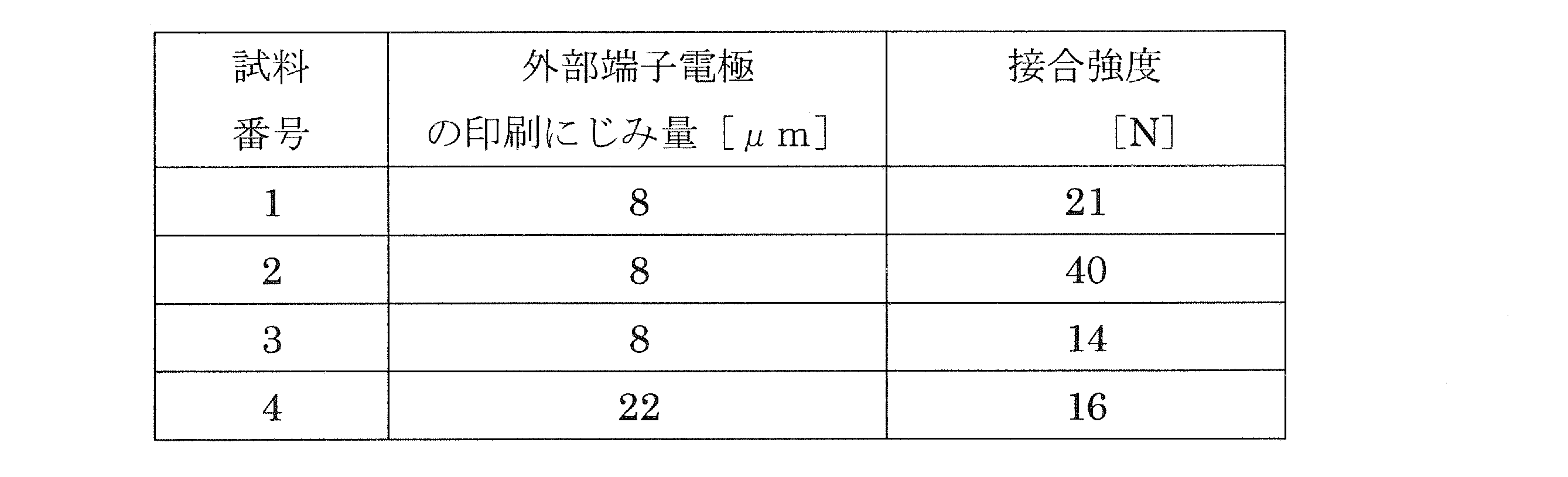
表1および表2からわかるように、外部端子電極の周縁部が中央部よりも厚い試料1および2によれば、試料3および4に比べて、接合強度が高められた。特に、被覆層が形成された試料2では、試料1に比べても、より高い接合強度が得られた。
これらに対して、外部端子電極の周縁部が中央部よりも薄い試料3および4では、高い接合強度が得られなかった。また、試料4では、外部端子電極の形成のために導電性ペーストの重ね塗りを行なったため、印刷にじみが大きく発生した。
次に、図7および図8を参照して、外部端子電極7の形成方法についての第2の実施形態を説明する。簡単に言えば、第2の実施形態は、第1の実施形態と比較して、周縁部8と中央部9との形成順序が逆であることを特徴としている。
まず、図7に示すように、導電性ペーストを用いて、外部端子電極7の中央部9がセラミックグリーンシート21上に比較的薄い膜厚をもって形成される。図7(B)には、中央部9の印刷のためのスクリーン版35が図示されている。スクリーン版35には、導電性ペーストの通過を許容する透過部36が設けられ、それ以外の領域は非透過部37とされている。
上記のように、周縁部8を形成する前に、中央部9を形成するようにすれば、中央部9を薄く形成することが容易である。
次に、図8に示すように、導電性ペーストを用いて、外部端子電極7の周縁部8がセラミックグリーンシート21上に比較的厚い膜厚をもって形成される。図8(B)には、周縁部8の印刷のためのスクリーン版38が図示されている。スクリーン版38には、導電性ペーストの通過を許容する透過部39が設けられ、それ以外の領域は非透過部40とされている。なお、周縁部8の厚みを前述した中央部9の厚みより厚く形成するため、たとえば、スクリーン版38の厚みはスクリーン版35の厚みより薄くされる。
図8に示した周縁部8は、中央部9の一部と重なるように形成されているが、中央部9とは重ならない状態で形成されてもよい。また、周縁部8は、そのすべてが中央部9と重なる状態で、すなわち、そのすべてが中央部9の上に乗る状態で形成されてもよい。
その後、前述した実施形態の場合と同様、被覆層11の形成工程、複数のセラミックグリーンシートの積層工程、プレス工程、焼成工程、めっき処理工程が順次実施され、図1に示したセラミック電子部品1が得られる。
第2の実施形態のように、中央部9を形成した後に、周縁部8を形成するようにしながら、その後に、被覆層11をスクリーン印刷によって形成する場合には、前述のように、中央部9をより薄く形成でき、そのため、より厚い周縁部8とより薄い中央部9との厚みの差をより大きくすることが容易であり、被覆層11の印刷のためのスクリーン版と周縁部8との密着性を高めることができるので、被覆層11のスクリーン印刷時のにじみを生じにくくすることができる。
以上説明した外部端子電極7の形成方法についての第1および第2の実施形態において、周縁部8を形成するための導電性ペーストと中央部9を形成するための導電性ペーストとで、有機溶剤の量を異ならせてもよい。すなわち、周縁部8用の導電性ペーストに含まれる有機溶剤の量を、中央部9用の導電性ペーストに含まれる有機溶剤の量より少なくすれば、周縁部8より厚く印刷することが容易になるとともに、中央部9をより薄く印刷することが容易になる。
また、周縁部8用の導電性ペーストおよび中央部9用の導電性ペーストとで、無機材料の含有量を異ならせておけば、以下のような利点が奏される。すなわち、ガラスや無機酸化物(Al2O3、ZrO2、MnO2など)といった無機材料の含有量に関して、周縁部8を形成するための導電性ペーストの方が、中央部9を形成するための導電性ペーストに比べて、より多くされると、焼成によって、無機材料はセラミックグリーンシート21中のセラミックに含まれるガラス成分との強固に結合するので、特に周縁部8での接合強度を向上させることができる。他方、無機材料が導電性ペーストに多く添加されると、焼結して得られた導体膜が緻密ではなくなり、外部からの水分の浸入が起こりやすくなる。したがって、中央部9を形成するための導電性ペーストにおいて、無機材料の含有量が比較的少なくされると、中央部9において緻密な導体膜が形成される。特に、図1からわかるように、中央部9は、比較的薄く形成され、また、部品本体3内部のビア導体5と接続されるので、緻密な導体膜であることが好ましい。
なお、上述の無機材料は、無機材料粉末の形で導電性ペーストに添加されても、金属粉末の粒子表面のコーティングした状態で添加されてもよい。
次に、図9および図10を参照して、外部端子電極の形成状態の変形例について説明する。図9および図10は、図6に対応する図である。図9および図10において、図6に示した要素に相当する要素には同様の参照符号を付し、重複する説明は省略する。
図9に示した外部端子電極7aは、その周縁部8の少なくとも一部を覆う被覆層が形成されていないことを特徴としている。
図10に示した外部端子電極7bは、その周縁部8の少なくとも一部を覆う被覆層が形成されていないばかりでなく、周縁部8の一部のみが部品本体3に埋め込まれていることを特徴としている。
次に、図11を参照して、外部端子電極の形成方法についての第3の実施形態を説明する。簡単に言えば、第3の実施形態は、外部端子電極7の周縁部8と中央部9とを同時に形成することを特徴としている。
この実施形態で用いられるスクリーン版41には、導電性ペーストの通過を許容する透過部42と、導電性ペーストの通過を禁止する非透過部43とが設けられるが、透過部42の領域内においては、その周縁部44に比べて、その中央部44がより厚くされ、中央部44が下方へ張り出す形状とされる。
このようなスクリーン版41を用いることにより、一度のスクリーン印刷によって、周縁部8の厚みが中央部9の厚みより厚い外部端子電極7を形成することができる。
以上、この発明を図示したいくつかの実施形態に関連して説明したが、この発明の範囲内において、その他種々の変形が可能である。
たとえば、上述の実施形態では、外部端子電極や被覆層の形成を、積層前のセラミックグリーンシートに対して行なったが、複数のセラミックグリーンシートを積層して得られた未焼成の部品本体における最表面に存在するセラミックグリーンシートに対して行なってもよい。
また、この発明は、積層構造を有する部品本体を備えるセラミック電子部品だけでなく、単層のセラミック層からなる部品本体を備えるセラミック電子部品に対しても適用することができる。
1 セラミック電子部品
2 セラミック層
3 部品本体
4 内部導体膜
5 ビア導体
6 主面
7,7a,7b 外部端子電極
8 周縁部
9 中央部
10 外部端子電極の表面
11 被覆層
12 被覆層の端部
13 めっき膜
21 セラミックグリーンシート
22,25,28,35,38,41 スクリーン版
2 セラミック層
3 部品本体
4 内部導体膜
5 ビア導体
6 主面
7,7a,7b 外部端子電極
8 周縁部
9 中央部
10 外部端子電極の表面
11 被覆層
12 被覆層の端部
13 めっき膜
21 セラミックグリーンシート
22,25,28,35,38,41 スクリーン版
Claims (23)
- セラミックをもって構成された部品本体と、
前記部品本体の主面に沿って設けられた外部端子電極と、
を備え、
前記外部端子電極が実装基板に電気的に接続されながら、実装基板上に実装される、セラミック電子部品であって、
前記外部端子電極は、周縁部と前記周縁部によって囲まれた中央部とを備え、前記周縁部の厚みは、前記中央部の厚みよりも厚く、かつ、前記周縁部の少なくとも一部が前記部品本体に埋め込まれている、
セラミック電子部品。 - 前記外部端子電極の表面と前記部品本体の前記主面とが同一面上に位置している、請求項1に記載のセラミック電子部品。
- 前記外部端子電極の前記周縁部の少なくとも一部を覆うように前記部品本体の前記主面に沿って形成された電気絶縁性の被覆層をさらに備える、請求項1または2に記載のセラミック電子部品。
- 前記被覆層の端部は、前記部品本体の前記主面において、前記外部端子電極の前記周縁部のうち最も厚みが厚い部分と接している、請求項3に記載のセラミック電子部品。
- 前記被覆層と前記外部端子電極の表面とが同一面上に位置している、請求項3または4に記載のセラミック電子部品。
- 前記外部端子電極の表面に形成されためっき膜をさらに備える、請求項1ないし5のいずれかに記載のセラミック電子部品。
- 前記外部端子電極の前記中央部と前記周縁部とは、互いに異なる組成を有する、請求項1ないし6のいずれかに記載のセラミック電子部品。
- 前記部品本体は、積層された複数のセラミック層をもって構成され、前記部品本体の内部に配置された内部導体をさらに備える、請求項1ないし7のいずれかに記載のセラミック電子部品。
- セラミックグリーンシートを用意する工程と、
前記セラミックグリーンシートの主面に導電性ペーストを用いて外部端子電極を形成する工程と、
前記外部端子電極が形成された前記セラミックグリーンシートを焼成する工程と、
を備え、
前記外部端子電極を形成する工程は、その周縁部の厚みが、前記周縁部によって囲まれた中央部の厚みよりも厚くなるように、前記外部端子電極を形成する工程を含む、
セラミック電子部品の製造方法。 - 前記外部端子電極を形成する工程は、前記周縁部と前記中央部とをそれぞれ別に形成する工程を含む、請求項9に記載のセラミック電子部品の製造方法。
- 前記周縁部を形成する工程の後に、前記中央部を形成する工程が実施される、請求項10に記載のセラミック電子部品の製造方法。
- 前記中央部を形成する工程の後に、前記周縁部を形成する工程が実施される、請求項10に記載のセラミック電子部品の製造方法。
- 前記周縁部を形成する工程で用いられる導電性ペーストと前記中央部を形成する工程で用いられる導電性ペーストとは、互いに異なる組成を有する、請求項10ないし12のいずれかに記載のセラミック電子部品の製造方法。
- 前記周縁部を形成する工程で用いられる導電性ペーストは、前記中央部を形成する工程で用いられる導電性ペーストに比べて、無機材料の含有量がより多くされる、請求項13に記載のセラミック電子部品の製造方法。
- 前記周縁部を形成する工程で用いられる導電性ペーストは、前記中央部を形成する工程で用いられる導電性ペーストに比べて、有機溶剤の量がより少なくされる、請求項13または14に記載のセラミック電子部品の製造方法。
- 前記焼成する工程の前に、前記外部端子電極が形成された前記セラミックグリーンシートをプレスする工程をさらに備える、請求項9ないし15のいずれかに記載のセラミック電子部品の製造方法。
- 前記プレスする工程は、前記外部端子電極の前記周縁部の少なくとも一部を前記セラミックグリーンシートに埋め込む工程を含む、請求項16に記載のセラミック電子部品の製造方法。
- 前記プレスする工程は、前記外部端子電極の表面が前記セラミックグリーンシートの主面と同一面上に位置するようにプレスする工程を含む、請求項17に記載のセラミック電子部品の製造方法。
- 前記焼成する工程の前に、前記外部端子電極の前記周縁部の少なくとも一部を覆うように前記セラミックグリーンシート上に電気絶縁性の被覆層を形成する工程をさらに備える、請求項9ないし15のいずれかに記載のセラミック電子部品の製造方法。
- 前記被覆層を形成する工程は、絶縁体ペーストをスクリーン印刷により塗布する工程を含む、請求項19に記載のセラミック電子部品の製造方法。
- 前記焼成する工程の前に、前記外部端子電極の表面と前記被覆層の表面とが同一面上に位置するように、前記外部端子電極および前記被覆層が形成された前記セラミックグリーンシートをプレスする工程をさらに備える、請求項19または20に記載のセラミック電子部品の製造方法。
- 前記外部端子電極の表面にめっき膜を形成する工程をさらに備える、請求項9ないし21のいずれかに記載のセラミック電子部品の製造方法。
- 前記セラミックグリーンシートを用意する工程において、複数のセラミックグリーンシートが用意され、前記複数のセラミックグリーンシートのうちの特定のものに対して前記外部端子電極を形成する工程が実施され、さらに、前記複数のセラミックグリーンシートのうちの特定のものに内部導体を形成する工程と、前記外部端子電極が一方の主面上に位置するように、前記複数のセラミックグリーンシートを積層する工程とを備える、請求項9ないし22のいずれかに記載のセラミック電子部品の製造方法。
Priority Applications (3)
| Application Number | Priority Date | Filing Date | Title |
|---|---|---|---|
| JP2013515068A JP5708798B2 (ja) | 2011-05-16 | 2012-04-27 | セラミック電子部品の製造方法 |
| CN201280023700.1A CN103535121B (zh) | 2011-05-16 | 2012-04-27 | 陶瓷电子元器件及其制造方法 |
| US14/068,053 US10178774B2 (en) | 2011-05-16 | 2013-10-31 | Ceramic electronic component and manufacturing method thereof |
Applications Claiming Priority (2)
| Application Number | Priority Date | Filing Date | Title |
|---|---|---|---|
| JP2011-109121 | 2011-05-16 | ||
| JP2011109121 | 2011-05-16 |
Related Child Applications (1)
| Application Number | Title | Priority Date | Filing Date |
|---|---|---|---|
| US14/068,053 Continuation US10178774B2 (en) | 2011-05-16 | 2013-10-31 | Ceramic electronic component and manufacturing method thereof |
Publications (1)
| Publication Number | Publication Date |
|---|---|
| WO2012157436A1 true WO2012157436A1 (ja) | 2012-11-22 |
Family
ID=47176771
Family Applications (1)
| Application Number | Title | Priority Date | Filing Date |
|---|---|---|---|
| PCT/JP2012/061364 Ceased WO2012157436A1 (ja) | 2011-05-16 | 2012-04-27 | セラミック電子部品およびその製造方法 |
Country Status (4)
| Country | Link |
|---|---|
| US (1) | US10178774B2 (ja) |
| JP (1) | JP5708798B2 (ja) |
| CN (1) | CN103535121B (ja) |
| WO (1) | WO2012157436A1 (ja) |
Cited By (7)
| Publication number | Priority date | Publication date | Assignee | Title |
|---|---|---|---|---|
| JP2018032773A (ja) * | 2016-08-25 | 2018-03-01 | 京セラ株式会社 | 電子部品搭載用基板、電子装置および電子モジュール |
| WO2021256561A1 (ja) * | 2020-06-18 | 2021-12-23 | 株式会社村田製作所 | 電子部品及び電子部品の製造方法 |
| WO2021256501A1 (ja) * | 2020-06-17 | 2021-12-23 | 株式会社村田製作所 | 電子部品及び電子部品の製造方法 |
| US11659659B2 (en) | 2018-11-08 | 2023-05-23 | Murata Manufacturing Co., Ltd. | Ceramic electronic component |
| WO2024150556A1 (ja) * | 2023-01-10 | 2024-07-18 | 株式会社村田製作所 | 電子部品 |
| WO2025028029A1 (ja) * | 2023-07-31 | 2025-02-06 | 株式会社村田製作所 | セラミック電子部品 |
| US12512263B2 (en) * | 2021-12-17 | 2025-12-30 | Murata Manufacturing Co., Ltd. | Ceramic electronic component |
Families Citing this family (3)
| Publication number | Priority date | Publication date | Assignee | Title |
|---|---|---|---|---|
| CN107851616B (zh) * | 2015-07-28 | 2020-07-31 | 京瓷株式会社 | 布线基板以及电子装置 |
| JP6699723B2 (ja) * | 2016-05-09 | 2020-05-27 | 株式会社村田製作所 | セラミック電子部品 |
| US11088090B1 (en) | 2020-02-12 | 2021-08-10 | Qualcomm Incorporated | Package comprising a substrate that includes a stress buffer layer |
Citations (3)
| Publication number | Priority date | Publication date | Assignee | Title |
|---|---|---|---|---|
| JPH08125341A (ja) * | 1994-10-25 | 1996-05-17 | Hitachi Ltd | 電子回路装置 |
| JP2004221407A (ja) * | 2003-01-16 | 2004-08-05 | Kyocera Corp | 配線基板 |
| WO2008053956A1 (fr) * | 2006-11-02 | 2008-05-08 | Murata Manufacturing Co., Ltd. | Substrat en céramique, dispositif électronique et procédé de production d'un substrat en céramique |
Family Cites Families (9)
| Publication number | Priority date | Publication date | Assignee | Title |
|---|---|---|---|---|
| JP2783751B2 (ja) * | 1993-12-21 | 1998-08-06 | 富士通株式会社 | 多層セラミック基板の製造方法 |
| JPH0858259A (ja) | 1994-08-19 | 1996-03-05 | Taiyo Yuden Co Ltd | スクリーン印刷用版 |
| JPH0864932A (ja) | 1994-08-25 | 1996-03-08 | Tokin Corp | メタライズ基板の製造方法 |
| JP4370663B2 (ja) | 2000-03-22 | 2009-11-25 | 株式会社村田製作所 | 積層型セラミック電子部品およびその製造方法ならびに電子装置 |
| US6861588B2 (en) * | 2002-07-16 | 2005-03-01 | Murata Manufacturing Co., Ltd. | Laminated ceramic electronic component and method of producing the same |
| JP3994936B2 (ja) | 2002-07-16 | 2007-10-24 | 株式会社村田製作所 | 積層型セラミック電子部品およびその製造方法 |
| JP2006335045A (ja) | 2005-06-06 | 2006-12-14 | Murata Mfg Co Ltd | スクリーン印刷版およびその製造方法、積層セラミック電子部品の製造方法 |
| US7388296B2 (en) * | 2005-06-09 | 2008-06-17 | Ngk Spark Plug Co., Ltd. | Wiring substrate and bonding pad composition |
| CN101933409B (zh) * | 2008-01-31 | 2013-03-27 | 株式会社村田制作所 | 陶瓷多层基板的制造方法及陶瓷多层基板 |
-
2012
- 2012-04-27 JP JP2013515068A patent/JP5708798B2/ja active Active
- 2012-04-27 WO PCT/JP2012/061364 patent/WO2012157436A1/ja not_active Ceased
- 2012-04-27 CN CN201280023700.1A patent/CN103535121B/zh active Active
-
2013
- 2013-10-31 US US14/068,053 patent/US10178774B2/en active Active
Patent Citations (3)
| Publication number | Priority date | Publication date | Assignee | Title |
|---|---|---|---|---|
| JPH08125341A (ja) * | 1994-10-25 | 1996-05-17 | Hitachi Ltd | 電子回路装置 |
| JP2004221407A (ja) * | 2003-01-16 | 2004-08-05 | Kyocera Corp | 配線基板 |
| WO2008053956A1 (fr) * | 2006-11-02 | 2008-05-08 | Murata Manufacturing Co., Ltd. | Substrat en céramique, dispositif électronique et procédé de production d'un substrat en céramique |
Cited By (8)
| Publication number | Priority date | Publication date | Assignee | Title |
|---|---|---|---|---|
| JP2018032773A (ja) * | 2016-08-25 | 2018-03-01 | 京セラ株式会社 | 電子部品搭載用基板、電子装置および電子モジュール |
| US11659659B2 (en) | 2018-11-08 | 2023-05-23 | Murata Manufacturing Co., Ltd. | Ceramic electronic component |
| WO2021256501A1 (ja) * | 2020-06-17 | 2021-12-23 | 株式会社村田製作所 | 電子部品及び電子部品の製造方法 |
| WO2021256561A1 (ja) * | 2020-06-18 | 2021-12-23 | 株式会社村田製作所 | 電子部品及び電子部品の製造方法 |
| US12342471B2 (en) | 2020-06-18 | 2025-06-24 | Murata Manufacturing Co., Ltd. | Electronic component and method for manufacturing electronic component |
| US12512263B2 (en) * | 2021-12-17 | 2025-12-30 | Murata Manufacturing Co., Ltd. | Ceramic electronic component |
| WO2024150556A1 (ja) * | 2023-01-10 | 2024-07-18 | 株式会社村田製作所 | 電子部品 |
| WO2025028029A1 (ja) * | 2023-07-31 | 2025-02-06 | 株式会社村田製作所 | セラミック電子部品 |
Also Published As
| Publication number | Publication date |
|---|---|
| CN103535121B (zh) | 2017-06-20 |
| JPWO2012157436A1 (ja) | 2014-07-31 |
| US10178774B2 (en) | 2019-01-08 |
| JP5708798B2 (ja) | 2015-04-30 |
| CN103535121A (zh) | 2014-01-22 |
| US20140057080A1 (en) | 2014-02-27 |
Similar Documents
| Publication | Publication Date | Title |
|---|---|---|
| JP5708798B2 (ja) | セラミック電子部品の製造方法 | |
| JP5855593B2 (ja) | 基板内蔵用積層セラミック電子部品及びその製造方法、基板内蔵用積層セラミック電子部品を備える印刷回路基板 | |
| JP4404139B2 (ja) | 積層型基板、電子装置および積層型基板の製造方法 | |
| JPWO2007063692A1 (ja) | セラミック基板、電子装置およびセラミック基板の製造方法 | |
| WO2011102040A1 (ja) | 素子搭載用基板およびその製造方法 | |
| WO2017199712A1 (ja) | セラミック電子部品 | |
| JP5582069B2 (ja) | セラミック多層基板 | |
| JP4900226B2 (ja) | 多層セラミック基板及びその製造方法、電子部品 | |
| JP7131628B2 (ja) | セラミック電子部品 | |
| JP5981389B2 (ja) | 配線基板 | |
| JP6026898B2 (ja) | セラミック配線基板 | |
| JP5383531B2 (ja) | 配線基板の製造方法 | |
| CN101129102A (zh) | 陶瓷基板、电子器件及陶瓷基板的制造方法 | |
| JP2009158668A (ja) | セラミック多層配線基板及びその製造方法 | |
| JP4711823B2 (ja) | 電子部品収納用パッケージおよび電子装置 | |
| JP2008112787A (ja) | 多層セラミックス基板及びその製造方法 | |
| WO2009151006A1 (ja) | セラミック成形体の製造方法 | |
| WO2023002894A1 (ja) | セラミック電子部品 | |
| JP4610185B2 (ja) | 配線基板並びにその製造方法 | |
| WO2007052619A1 (ja) | 積層セラミック基板の製造方法 | |
| JP2004179259A (ja) | 回路基板およびその製造方法 | |
| JP2008159726A (ja) | 多層配線基板 | |
| WO2013001973A1 (ja) | 多層セラミック基板およびその製造方法ならびに電子部品モジュール | |
| JP6185695B2 (ja) | 多層配線基板およびその製造方法 | |
| JP2008112786A (ja) | 多層セラミックス基板及びその製造方法 |
Legal Events
| Date | Code | Title | Description |
|---|---|---|---|
| 121 | Ep: the epo has been informed by wipo that ep was designated in this application |
Ref document number: 12785012 Country of ref document: EP Kind code of ref document: A1 |
|
| ENP | Entry into the national phase |
Ref document number: 2013515068 Country of ref document: JP Kind code of ref document: A |
|
| NENP | Non-entry into the national phase |
Ref country code: DE |
|
| 122 | Ep: pct application non-entry in european phase |
Ref document number: 12785012 Country of ref document: EP Kind code of ref document: A1 |