WO2012137398A1 - 有機エレクトロルミネッセンス素子 - Google Patents
有機エレクトロルミネッセンス素子 Download PDFInfo
- Publication number
- WO2012137398A1 WO2012137398A1 PCT/JP2012/001045 JP2012001045W WO2012137398A1 WO 2012137398 A1 WO2012137398 A1 WO 2012137398A1 JP 2012001045 W JP2012001045 W JP 2012001045W WO 2012137398 A1 WO2012137398 A1 WO 2012137398A1
- Authority
- WO
- WIPO (PCT)
- Prior art keywords
- layer
- light
- light extraction
- electrode layer
- organic
- Prior art date
- Legal status (The legal status is an assumption and is not a legal conclusion. Google has not performed a legal analysis and makes no representation as to the accuracy of the status listed.)
- Ceased
Links
Images
Classifications
-
- G—PHYSICS
- G02—OPTICS
- G02B—OPTICAL ELEMENTS, SYSTEMS OR APPARATUS
- G02B5/00—Optical elements other than lenses
- G02B5/02—Diffusing elements; Afocal elements
- G02B5/0205—Diffusing elements; Afocal elements characterised by the diffusing properties
- G02B5/0236—Diffusing elements; Afocal elements characterised by the diffusing properties the diffusion taking place within the volume of the element
- G02B5/0242—Diffusing elements; Afocal elements characterised by the diffusing properties the diffusion taking place within the volume of the element by means of dispersed particles
-
- H—ELECTRICITY
- H10—SEMICONDUCTOR DEVICES; ELECTRIC SOLID-STATE DEVICES NOT OTHERWISE PROVIDED FOR
- H10K—ORGANIC ELECTRIC SOLID-STATE DEVICES
- H10K50/00—Organic light-emitting devices
- H10K50/80—Constructional details
- H10K50/85—Arrangements for extracting light from the devices
- H10K50/854—Arrangements for extracting light from the devices comprising scattering means
-
- H—ELECTRICITY
- H10—SEMICONDUCTOR DEVICES; ELECTRIC SOLID-STATE DEVICES NOT OTHERWISE PROVIDED FOR
- H10K—ORGANIC ELECTRIC SOLID-STATE DEVICES
- H10K2102/00—Constructional details relating to the organic devices covered by this subclass
- H10K2102/301—Details of OLEDs
- H10K2102/331—Nanoparticles used in non-emissive layers, e.g. in packaging layer
Definitions
- the present invention relates to an organic electroluminescence element having a light extraction layer.
- An electroluminescence (EL) element is formed by forming a light emitting layer sandwiched between an anode and a cathode on a transparent substrate. When a voltage is applied between the electrodes, electrons and holes injected as carriers in the light emitting layer are formed. Light is emitted by excitons generated by recombination.
- EL elements are roughly classified into an organic EL element using an organic substance as a fluorescent material of a light emitting layer and an inorganic EL element using an inorganic substance.
- the organic EL element can emit light with high luminance at a low voltage, and various emission colors can be obtained depending on the type of fluorescent material.
- various types of organic EL elements can be easily manufactured as a flat light-emitting panel. Used as a display device or a backlight. Furthermore, in recent years, a device corresponding to high luminance has been realized and attention has been paid to using it for a lighting fixture.
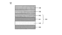
- FIG. 3 shows a cross-sectional configuration of a general organic EL element.
- a light-transmitting anode layer 102 is provided on a light-transmitting substrate 106, and a hole transport layer 142, a light emitting layer 141, and an electron transport layer 143 are formed on the anode layer 102.
- An organic layer 104 is provided.
- a light-reflecting cathode layer 103 is provided on the organic layer 104. Then, when a voltage is applied between the anode layer 102 and the cathode layer 103, light emitted from the organic layer 104 is transmitted through the anode layer 102 and the substrate 106 and extracted.
- the critical angle is determined from Snell's law by the refractive index between the medium at the interface, and all light above the critical angle is transmitted at the interface. Reflected, confined in a medium having a high refractive index, and lost as guided light.
- glass is widely used as the substrate 106 used in the general organic EL element 101 from the viewpoint of transparency, strength, low cost, gas barrier layer, chemical resistance, heat resistance, etc.
- the refractive index of a soda lime glass or the like is about 1.52.
- ITO indium tin oxide
- IZO indium zinc oxide
- ITO or IZO indium zinc oxide
- the refractive index of ITO or IZO varies depending on the composition, film formation method, crystal structure, etc., but the refractive index of ITO is about 1.7 to 2.3, and the refractive index of IZO is 1.9 to 2.4. Both have a higher refractive index than the substrate 106.
- the refractive index of each material such as a light emitting material constituting the light emitting layer 141, the hole transport layer 142, the electron transport layer 143 and the like used for the organic layer 104 is often about 1.6 to 2.0. That is, in the general organic EL element 101, the refractive index of each layer is in the relationship of air ⁇ substrate ⁇ organic layer ⁇ anode. Therefore, among the light emitted from the light emitting source of the light emitting layer 141 of the organic EL element 101, the light incident at a large incident angle on the interface between the substrate 6 and the outside of the element (atmosphere) and the interface between the anode 1 and the substrate 6 is Therefore, effective light may not be extracted outside the device.
- a light extraction layer composed of a layer having a light scattering function or the like is provided, so that the light use efficiency of the light emitted from the light emitting layer 141 is increased.
- An improved organic EL device is known (for example, see Japanese Patent Application Laid-Open No. 2006-286616).
- the light scattering layer containing light scattering particles is used as a part of the light extraction layer.
- the surface of the light scattering particle layer is uneven due to the presence of the light scattering particles. If the surface is uneven, the anode, the organic layer, and the cathode cannot be laminated with a uniform thickness. Therefore, a smoothing layer that smoothes the surface is formed on the upper surface side of the light scattering particle layer.
- this smoothing layer is laminated on the light extraction layer, voids may be generated at the interface between the light scattering particles and the smooth layer, and the light extraction layer does not function sufficiently due to the voids, and the light extraction efficiency is reduced. There was a risk of lowering.
- the present invention solves the above-mentioned problems, and the light extraction layer can be a single layer, and the generation of voids at the interface between the base material and the light scattering particles is suppressed to improve the light extraction efficiency.
- An object of the present invention is to provide an organic EL element that can be used.
- an organic electroluminescence device includes an organic layer provided between a first electrode layer and a second electrode layer, the first electrode layer, and the second electrode.
- a light extraction layer that is provided on at least one surface of the layer and changes the directivity of light, and a substrate provided on the light extraction layer, the light extraction layer constituting the light extraction layer It contains a base material and 1 to 5% by weight of light scattering particles with respect to the base material.
- the light scattering particles preferably have a particle size of 0.1 to 10 ⁇ m.
- the light scattering particles are preferably particles having different shapes in the major axis direction and the minor axis direction.
- the light scattering particles preferably have an uneven shape on the surface.
- a difference between a refractive index of a base material constituting the light extraction layer and a refractive index of the light scattering particles is 0.15 to 0.45.
- the refractive index of the base material constituting the light extraction layer and the refractive index of the first electrode layer or the second electrode layer in contact with the light extraction layer are substantially equal. It is preferable.
- the light extraction layer contains 1 to 5% by weight of light scattering particles with respect to the base material, even a single layer can sufficiently improve the light extraction efficiency. If the light scattering particles are 1 to 5% by weight, it is difficult to generate voids at the interface between the light scattering particle base material and the light scattering particles, and the light extraction efficiency can be further improved.
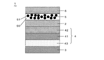
- FIG. 1 is a side sectional view of an organic electroluminescence element according to an embodiment of the present invention.
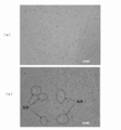
- A is a figure which shows the microscope picture of the surface of the light extraction layer produced by adding 5 weight% of light-scattering particles with respect to a base material on the board
- (b) The figure which is a comparative example of the same organic electroluminescent element, Comprising: The figure which shows the microscope picture of the surface of the light extraction layer produced by adding 7.5 weight% of light-scattering particles with respect to a base material on a board
- the organic EL element 1 of the present embodiment includes an organic layer 4 provided between the first electrode layer 2 and the second electrode layer 3, and at least one of the first electrode layer 2 and the second electrode layer 3. And a substrate 6 provided on the light extraction layer 5.
- the light extraction layer 5 is provided on the surface of the light extraction layer 5 to change the directivity of light.
- the first electrode layer 2 functions as an anode for supplying holes to the hole transport layer 42
- the second electrode layer 3 functions as a cathode for injecting electrons into the light emitting layer 41.
- the first electrode layer 2 and the substrate 6 are translucent, and the second electrode layer 3 is light reflective.
- the light extraction layer 5 is provided on one surface of the first electrode layer 2 is shown.
- the organic EL element 1 configured as described above, when light is applied between the first electrode layer 2 and the second electrode layer 3, light emitted from the light emitting layer 41 of the organic layer 4 is The light passes through the first electrode layer 2 and the substrate 6 and is taken out of the device.
- the organic layer 4 includes an electron transport layer 43 provided between the second electrode layer 3 and the light emitting layer 41, the first electrode layer 2, and the light emitting layer.
- the structure provided with the hole transport layer 42 provided between 41 is shown, it is not restricted to this structure.
- the light emitting layer 41 may be a stack of a plurality of light emitting layers.
- the substrate 6 for example, a transparent glass plate such as soda lime glass or non-alkali glass, a plastic film or a plastic plate produced by an arbitrary method from a resin such as polyester, polyolefin, polyamide, or epoxy, a fluorine resin, or the like Is used.
- substrate 6 may be the glass which mixed heavy metals, such as lead, and can use arbitrary things.
- the light extraction layer 5 is formed from a composition in which 1 to 5% by weight of light scattering particles 51 are mixed with the base material 50 constituting the light extraction layer 5.
- the base material 50 a material having excellent translucency and having a refractive index substantially equal to that of the first electrode layer 2 or the second electrode layer 3 in contact with the light extraction layer 5 is preferably used. Resin, thiourethane resin and the like are used.
- the light scattering particles 51 translucent fine particles such as silica and alumina are used. When the concentration of the light scattering particles 51 is less than 1% by weight, a sufficient light extraction effect cannot be obtained.
- the concentration of the light scattering particles 51 exceeds 5% by weight, the substrate 6 in contact with the light extraction layer 5 may be cracked.
- 5% by weight, 7.5% by weight, or 10% by weight of light scattering particles 51 are dispersed in the imide resin used as the base material 50, applied to the glass substrate 6 and dried to extract light.
- the layer 5 was produced, and micrographs of the surface are shown in FIGS. 2 (a) and 2 (b), respectively.
- imide resin made by OPTMATE and methyl silicone particles made by GE Toshiba Silicone (particle diameter: 2 ⁇ m) were used.
- the light extraction layer to which 7.5 wt% of the light scattering particles 51 was added to the base material 50 had cracks on the surface of the substrate 6. This crack causes a short circuit and reduces the reliability of the device.
- the light extraction layer 5 to which the light scattering particles 51 of 5% by weight with respect to the base material 50 are added does not cause cracks on the surface of the substrate 6 as shown in FIG. It was.
- the particle diameter of the light scattering particles 51 is preferably 0.05 to 10 ⁇ m. If the particle diameter of the light scattering particles 51 is less than 0.05 ⁇ m, the effect of scattering light cannot be sufficiently obtained, and the light extraction efficiency cannot be sufficiently increased. On the other hand, when the particle diameter of the light scattering particles 51 exceeds 10 ⁇ m, the flatness on the surface of the light extraction layer 5 opposite to the substrate 6 may be deteriorated.
- the shape of the light scattering particle 51 may be an isotropic shape such as a spherical shape, but is preferably a particle having a different shape in the major axis direction and the minor axis direction. If the light scattering particles 51 have an anisotropic shape, the major axis direction thereof is arranged at various angles and directions with respect to the film thickness direction of the light extraction layer 5 to improve the light scattering effect of the light scattering particles 51. be able to.
- the light scattering particles 51 When the light extraction layer 5 is formed by coating on the surface of the substrate 6 using the anisotropic light scattering particles 51, the light scattering particles 51 have a major axis direction of the substrate unless special treatment or the like is performed. It is not arranged regularly in one direction, such as parallel to the surface of 6, but is arranged in an irregular direction. Therefore, the anisotropic light scattering particles 51 can enhance the light scattering effect in all directions as compared to the spherical light scattering particles 51. Therefore, by using the anisotropic light scattering particles 51 having the major axis direction and the minor axis direction in the light extraction layer 5, it is possible to scatter light in an oblique direction while suppressing reduction of front extraction light, The light extraction efficiency can be further improved.
- the major axis direction and the minor axis direction of the light scattering particles 51 are not necessarily orthogonal to each other, and may have an anisotropic shape in which the major axis direction and the minor axis direction are at an arbitrary angle.
- the particle size in the major axis direction and the particle size in the minor axis direction of the anisotropic light scattering particles 51 are preferably in the range of 0.05 to 10 ⁇ m as described above.
- the difference between the major axis direction and the minor axis direction particle size is preferably in the range of 1.2 to 5 with the minor axis direction particle size being 1. If the particle diameter in the major axis direction exceeds 5, the flatness on the surface opposite to the substrate 6 of the light extraction layer 5 may be deteriorated, which is not preferable.
- the surface of the light scattering particle 51 may be flat, but preferably has an uneven shape.
- the surface of the light scattering particle 51 has an uneven shape, the light scattering effect can be increased and the light extraction efficiency can be further improved as compared with the case where the surface is flat.
- the light scattering particles 51 those having a refractive index smaller than that of the base material 50 constituting the light extraction layer 5 are used. In this way, the light incident on the base material 50 can be totally reflected on the surface of the light scattering particles 51 and scattered in various directions.
- the difference between the refractive index of the base material 50 constituting the light extraction layer 5 and the refractive index of the light scattering particles 51 is preferably 0.15 to 0.45. When this difference is less than 0.15, the light totally reflected on the surface of the light scattering particles 51 is reduced, and a sufficient light scattering function cannot be obtained.
- the refractive index of the translucent resin used as the base material 50 is usually about 1.4 to 1.8, the difference in refractive index from the base material 50 is 0.45 or more. It is not easy to use a low refractive index material for the light scattering particles 51.
- the light transmittance of the light extraction layer 5 is preferably at least 50% or more, more preferably 80% or more.
- the light extraction layer 5 is preferably designed so that total reflection at the interface with the first electrode layer 2 is difficult to occur. That is, the refractive index of the base material 50 of the light extraction layer 5 is preferably substantially the same as that of the first electrode layer 2.
- substantially equal means that the refractive index difference is ⁇ 0.2 or less.
- an electrode material made of a metal, an alloy, an electrically conductive compound, or a mixture thereof having a high work function is used so that holes can be efficiently injected into the organic layer 4. It is particularly preferable to use a material having a work function of 4 eV or more.
- the material of the first electrode layer 2 include metals such as gold, CuI, ITO (indium-tin oxide), SnO 2 , ZnO, IZO (indium-zinc oxide), and GZO (gallium- Zinc oxide), conductive polymers such as PEDOT and polyaniline, conductive polymers doped with any acceptor, and conductive light-transmitting materials such as carbon nanotubes.
- the 1st electrode layer 2 can be produced by forming the electrode material mentioned above in the thin film by methods, such as a vacuum evaporation method, sputtering method, application
- the transmittance of the second electrode layer 3 is preferably 70% or more.
- the sheet resistance of the second electrode layer 3 is preferably several hundred ⁇ / ⁇ or less, and more preferably 100 ⁇ / ⁇ or less.
- the film thickness of the first electrode layer 2 varies depending on the characteristics such as the conductivity of the material, but in order to control the characteristics such as the light transmittance and the sheet resistance of the first electrode layer 2 as described above, it is 500 nm. The following is preferable, and a range of 10 to 200 nm is more preferable.
- the first electrode layer 2 is preferably configured such that the surface opposite to the light extraction layer 5 has high flatness in order to prevent leakage current and short circuit.
- the organic layer 4 is formed by stacking the hole transport layer 42, the light emitting layer 41, and the electron transport layer 43 described above, and an electron transport layer, a hole block layer, an electron injection layer, or the like (not shown) on the light emitting layer 41. These appropriate organic layers may be laminated.
- the light emitting layer 41 may be formed in a plurality of layers. As described above, when a plurality of the light emitting layers 41 are provided, the number of stacked layers is preferably 5 or less, more preferably 3 or less because the difficulty of optical and electrical element design increases as the number of layers increases. . In this case, it is preferable to interpose a charge supply layer (not shown) between the plurality of organic layers 4.
- the charge supply layer examples include metal thin films such as Ag, Au, and Al, metal oxides such as vanadium oxide, molybdenum oxide, rhenium oxide, and tungsten oxide, ITO, IZO, AZO, GZO, ATO, and SnO 2 .
- Transparent conductive film so-called stack of n-type semiconductor and p-type semiconductor, metal thin film or stack of transparent conductive film and n-type semiconductor and / or p-type semiconductor, mixture of n-type semiconductor and p-type semiconductor, n-type semiconductor Alternatively, a mixture of a p-type semiconductor and a metal can be used.
- the n-type semiconductor or p-type semiconductor may be an inorganic material or an organic material. Furthermore, it may be obtained by a mixture of organic material and metal, organic material and metal oxide, organic material and organic acceptor / donor material, inorganic acceptor / donor material, etc. Select and use.
- the hole transport layer 42 is appropriately selected from a group of compounds having hole transport properties.
- this type of compound include 4,4′-bis [N- (naphthyl) -N-phenyl-amino] biphenyl ( ⁇ -NPD), N, N′-bis (3-methylphenyl)-(1 , 1′-biphenyl) -4,4′-diamine (TPD), 2-TNATA, 4,4 ′, 4 ′′ -tris (N- (3-methylphenyl) N-phenylamino) triphenylamine (MTDATA) 4,4'-N, N'-dicarbazole biphenyl (CBP), spiro-NPD, spiro-TPD, spiro-TAD, TNB, and the like, triarylamine compounds, amine compounds containing carbazole groups, fluorene Examples thereof include amine compounds containing derivatives, etc. It is not limited to those described above, and any generally known hole transporting material can be used.
- Examples of the organic EL material constituting the light emitting layer 41 include anthracene, naphthalene, pyrene, tetracene, coronene, perylene, phthaloperylene, naphthaloperylene, diphenylbutadiene, tetraphenylbutadiene, coumarin, oxadiazole, bisbenzoxazoline, bisstyryl, Cyclopentadiene, quinoline metal complex, tris (8-hydroxyquinolinato) aluminum complex (Alq 3 ), tris (4-methyl-8-quinolinato) aluminum complex, tris (5-phenyl-8-quinolinato) aluminum complex, amino Quinoline metal complex, benzoquinoline metal complex, tri- (p-terphenyl-4-yl) amine, 1-aryl-2,5-di (2-thienyl) pyrrole derivative, pyran, quinacridone, rubrene, dis Rirubenzen derivatives, distyryl arylene
- the light emitting material selected from these compounds suitably.
- so-called phosphorescent materials for example, luminescent materials such as Ir complexes, Os complexes, Pt complexes, and europium complexes, or compounds having these in the molecule or high Molecules can also be suitably used. These materials are appropriately selected and used as necessary.
- the light emitting layer 41 made of the above-described material may be formed by a dry process such as vapor deposition or transfer, or may be formed by a wet process such as spin coating, spray coating, die coating, or gravure printing. .
- the electron transport layer 43 is formed from a material appropriately selected from the group of compounds having electron transport properties.
- this type of compound include metal complexes known as electron transporting materials such as Alq 3 and compounds having a heterocyclic ring such as phenanthroline derivatives, pyridine derivatives, tetrazine derivatives, and oxadiazole derivatives.
- metal complexes known as electron transporting materials such as Alq 3
- compounds having a heterocyclic ring such as phenanthroline derivatives, pyridine derivatives, tetrazine derivatives, and oxadiazole derivatives.
- Arbitrary well-known arbitrary electron transport materials can be used.
- the second electrode layer 3 is preferably made of an electrode material made of a metal, an alloy, an electrically conductive compound and a mixture thereof having a low work function so that electrons can be efficiently injected into the light emitting layer 41. It is particularly preferable that the work function is 5 eV or less.
- the material constituting the second electrode layer 5 include alkali metals, alkali metal halides, alkali metal oxides, alkaline earth metals, and alloys of these with other metals. Specifically, aluminum (Al), silver (Ag), or a compound containing these metals can be used. Moreover, you may comprise as a laminated structure etc. combining Al and another electrode material.
- Such electrode material combinations include alkali metal and Al laminates, alkali metal and silver laminates, alkali metal halides and Al laminates, and alkali metal oxides and Al laminates.
- Body alkaline earth metal or laminate of rare earth metal and Al, alloys of these metal species with other metals, and the like.
- a laminate of sodium (Na), Na-potassium (K) alloy, lithium (Li), magnesium (Mg), etc. and Al Mg-Ag mixture, Mg-indium mixture, Al-Li Examples include alloys, LiF / Al mixtures / laminates, Al / Al 2 O 3 mixtures, and the like.
- an alkali metal oxide, an alkali metal halide, or a metal oxide may be used as the base of the second electrode layer 3 and one or more conductive materials such as metals may be stacked and used. Examples of these include, for example, an alkali metal / Al laminate, an alkali metal halide / alkaline earth metal / Al laminate, an alkali metal oxide / Al laminate, and the like.
- a layer that promotes electron injection from the second electrode layer 3 (cathode) to the light emitting layer 41 that is, an electron injection layer (not shown) is interposed between the cathode and the light emitting layer. It is preferable to insert.
- a material constituting the electron injection layer As a material constituting the electron injection layer, a material common to the material constituting the second electrode layer 3, a metal oxide such as titanium oxide and zinc oxide, and a dopant that promotes electron injection, including the above materials, are used. Examples include, but are not limited to, mixed organic semiconductor materials.
- the second electrode layer 3 may be composed of a combination of a transparent electrode and a light reflective layer.
- the transparent electrode represented by ITO, IZO, etc.
- the organic layer at the interface of the second electrode layer 3 may be doped with an alkali metal such as lithium, sodium, cesium, or calcium, or an alkaline earth metal.
- Examples of the method for producing the second electrode layer 3 include forming the electrode material described above into a thin film by a method such as vacuum deposition, sputtering, or coating.
- the reflectance is preferably 80% or more, and more preferably 90% or more.
- the light transmittance of the second electrode layer 3 is preferably 70% or more.
- the thickness of the third electrode layer 5 varies depending on the material in order to control characteristics such as light transmittance of the third electrode layer 5, but is preferably 500 nm or less, preferably 100 to 200 nm. A range is particularly preferred.
- a non-alkali glass plate (No. 1737; manufactured by Corning) having a thickness of 0.7 mm was used as the substrate 6, and the coating material composition obtained on the glass surface was applied and dried by a spin coater at 1000 rpm.
- sputtering was performed using an ITO (tin-doped indium oxide) target (manufactured by Tosoh Corporation) to form a 150 nm ITO film.
- ITO in-doped indium oxide
- the glass substrate with ITO was subjected to ultrasonic cleaning with pure water, acetone, and isopropyl alcohol for 10 minutes each, then steam cleaned with isopropyl alcohol vapor for 2 minutes, dried, and further UV ozone cleaned for 10 minutes. Subsequently, this ITO layer-coated glass substrate was set in a vacuum deposition apparatus, and 4,4′-bis [N- (naphthyl) -N-phenyl-amino] biphenyl ( ⁇ -NPD) under a reduced pressure of 5 ⁇ 10 ⁇ 5 Pa. ) was deposited to a thickness of 40 nm to form a hole transport layer 42 on the first electrode layer 2 (ITO).
- a light emitting layer 41 in which Alq3 was doped with 6% rubrene was provided with a thickness of 30 nm. Further, TpPyPhB was deposited to a thickness of 65 nm as the electron transport layer 43. Further, LiF was deposited to a thickness of 1 nm as an electron injection layer (not shown), and Al was deposited to a thickness of 80 nm as the second electrode layer 3 (cathode), thereby producing the organic EL element 1 of Example 1.
- the organic EL element 1 of Example 2 was produced.
- surface irregular fine particles Matsumoto Yushi Seiyaku Co., Ltd .
- Matsumoto Microsphere M, particle size 5 ⁇ m, nD 1.5
- the “condensed compound equivalent” is the mass that Si present is SiO 2 in the case of tetraalkoxysilane, and the mass that is SiO 1.5 in the case of trialkoxysilane.
- a non-alkali glass plate (No. 1737, manufactured by Corning) having a thickness of 0.7 mm was used as the substrate 6, and the coating material composition obtained on the glass surface was applied and dried by a spin coater at 1000 rpm. After repeating coating and drying 6 times, heat treatment was performed by baking at 200 ° C. for 30 minutes.
- a film was formed by drying, and heat treatment was performed by baking at 200 ° C. for 30 minutes, and a planarizing layer having a thickness of about 4 ⁇ m was laminated.
- An organic EL device of Comparative Example 1 was obtained in the same manner as in Example 1 except that the light extraction layer was produced by the above procedure.
- the light extraction layer 5 is a single layer. That is, by forming the base material 50 and the light scattering particles 51 of 5% by weight with respect to the base material 50, it is difficult for voids to be generated at the interface between the base material 50 and the light scattering particles 51. Light loss can be suppressed and light extraction efficiency can be improved. Although not described in Table 1 above, it was confirmed that the light scattering efficiency was improved by setting the light scattering particles 51 to 1 wt% or more with respect to the base material 50.
- the planarization layer is not formed in the light extraction layer 5, but the external quantum efficiency is higher than that of Comparative Example 1 in which the planarization layer is formed.
- the particle diameter of the light scattering particles is reduced (substantially 0.1 to 10 ⁇ m)
- the light extraction layer 5 faces the first electrode layer 5 (or the second electrode layer 3).
- the surface unevenness can be reduced, and light emission equivalent to or higher than that in the case where the planarization layer is provided is possible.
- the first electrode layer 5 formed on the light extraction layer 5 can also be made uniform with less unevenness. As a result, the risk of an element short circuit can be reduced, and the reliability of a device using the organic EL element 1 can be improved.
- Example 2 the external quantum efficiency exceeding that of Example 1 is shown.
- the anisotropically shaped light scattering particles 51 convex lens-shaped acrylic resin particles
- Example 3 the external quantum efficiency which exceeds Example 1 is shown. This result shows that the light scattering effect can be improved and the light extraction efficiency can be further improved by using the light scattering particles 51 having an uneven shape on the surface as in Example 3.
- Example 1 the difference between the refractive index of the base material 50 constituting the light extraction layer 5 and the refractive index of the light scattering particles 51 is 0.15 or more. In Example 1, the refractive index difference is less than 0.15. In Examples 1 to 3, external quantum efficiencies exceeding Comparative Example 1 are shown. This result shows that the suitable light scattering characteristic by the light-scattering particle
- the refractive index of the base material 50 constituting the light extraction layer 5 substantially the same as the refractive index of the first electrode layer 2 (anode), the light transmitted through the first electrode layer 2 is The light can be incident on the light extraction layer 5 and scattered by the light scattering particles 51 without being totally reflected at the interface with the light extraction layer 5.
- the light extraction layer 5 containing 1 to 5 wt% of light scattering particles 51 with respect to the base material 50 is provided on at least one surface of the first electrode layer 2 or the second electrode layer 3. If provided, the present invention is not limited to the above embodiment, and various modifications are possible. For example, a material other than the light scattering particles 51 may be added to the base material 50 constituting the light extraction layer 5. In addition, a layer configured in the same manner as the light extraction layer 5 described above may be provided outside the substrate 6.
Landscapes
- Physics & Mathematics (AREA)
- Optics & Photonics (AREA)
- Chemical & Material Sciences (AREA)
- Dispersion Chemistry (AREA)
- General Physics & Mathematics (AREA)
- Electroluminescent Light Sources (AREA)
- Optical Elements Other Than Lenses (AREA)
Priority Applications (1)
| Application Number | Priority Date | Filing Date | Title |
|---|---|---|---|
| US14/007,091 US20140008635A1 (en) | 2011-04-05 | 2012-02-17 | Organic electroluminescence element |
Applications Claiming Priority (2)
| Application Number | Priority Date | Filing Date | Title |
|---|---|---|---|
| JP2011083316A JP5824678B2 (ja) | 2011-04-05 | 2011-04-05 | 有機エレクトロルミネッセンス素子 |
| JP2011-083316 | 2011-04-05 |
Publications (1)
| Publication Number | Publication Date |
|---|---|
| WO2012137398A1 true WO2012137398A1 (ja) | 2012-10-11 |
Family
ID=46968817
Family Applications (1)
| Application Number | Title | Priority Date | Filing Date |
|---|---|---|---|
| PCT/JP2012/001045 Ceased WO2012137398A1 (ja) | 2011-04-05 | 2012-02-17 | 有機エレクトロルミネッセンス素子 |
Country Status (4)
| Country | Link |
|---|---|
| US (1) | US20140008635A1 (enExample) |
| JP (1) | JP5824678B2 (enExample) |
| TW (1) | TW201301612A (enExample) |
| WO (1) | WO2012137398A1 (enExample) |
Cited By (3)
| Publication number | Priority date | Publication date | Assignee | Title |
|---|---|---|---|---|
| US20150008422A1 (en) * | 2012-03-23 | 2015-01-08 | Lg Chem, Ltd. | Organic light emitting device |
| EP2973774A1 (en) * | 2013-03-12 | 2016-01-20 | PPG Industries Ohio, Inc. | Organic light emitting diode with light extracting layer |
| CN106935725A (zh) * | 2017-02-17 | 2017-07-07 | 武汉华星光电技术有限公司 | 有机电致发光显示装置 |
Families Citing this family (10)
| Publication number | Priority date | Publication date | Assignee | Title |
|---|---|---|---|---|
| US9806294B2 (en) * | 2013-03-28 | 2017-10-31 | Konica Minolta, Inc. | Surface light emitting element |
| TWI511344B (zh) * | 2013-05-08 | 2015-12-01 | Ind Tech Res Inst | 光取出元件及發光裝置 |
| JP6127791B2 (ja) * | 2013-07-16 | 2017-05-17 | 東洋インキScホールディングス株式会社 | 光散乱層用樹脂組成物、光散乱層、および有機エレクトロルミネッセンス装置 |
| JP6503363B2 (ja) | 2013-09-17 | 2019-04-17 | エルジー ディスプレイ カンパニー リミテッド | 有機発光素子 |
| JP6163096B2 (ja) * | 2013-12-17 | 2017-07-12 | 日揮触媒化成株式会社 | 高屈折率無機平坦化層形成用塗料およびその製造方法 |
| JP6201807B2 (ja) * | 2014-02-20 | 2017-09-27 | コニカミノルタ株式会社 | 有機発光素子の製造方法及び有機発光素子 |
| KR102368894B1 (ko) * | 2016-09-30 | 2022-03-02 | 코오롱인더스트리 주식회사 | 광확산 기능을 부여한 봉지층 조성물 및 이를 이용하여 제조된 유기발광소자 |
| WO2018142721A1 (ja) * | 2017-01-31 | 2018-08-09 | 日本板硝子株式会社 | 光拡散粒子、光拡散透過シート、及び光拡散粒子を製造する方法 |
| WO2018142722A1 (ja) * | 2017-01-31 | 2018-08-09 | 日本板硝子株式会社 | 光拡散粒子、光拡散透過シート、及び光拡散粒子を製造する方法 |
| JP2018185940A (ja) * | 2017-04-25 | 2018-11-22 | 五洋紙工株式会社 | El素子用光取出しフィルム |
Citations (6)
| Publication number | Priority date | Publication date | Assignee | Title |
|---|---|---|---|---|
| JP2006294491A (ja) * | 2005-04-13 | 2006-10-26 | Seiko Epson Corp | エレクトロルミネッセンス装置、エレクトロルミネッセンス装置の製造方法、電子機器 |
| JP2008016347A (ja) * | 2006-07-06 | 2008-01-24 | Toppan Printing Co Ltd | 有機エレクトロルミネッセンス素子 |
| JP2009004275A (ja) * | 2007-06-22 | 2009-01-08 | Panasonic Electric Works Co Ltd | 面発光体及び面発光体の製造方法 |
| JP2009110930A (ja) * | 2007-08-21 | 2009-05-21 | Fujifilm Corp | 散乱部材、及びこれを用いた有機エレクトロルミネッセンス表示装置 |
| WO2011111670A1 (ja) * | 2010-03-08 | 2011-09-15 | パナソニック電工株式会社 | 有機エレクトロルミネッセンス素子 |
| JP2011248104A (ja) * | 2010-05-27 | 2011-12-08 | Jsr Corp | 光取り出しフィルムおよびその製造方法 |
Family Cites Families (7)
| Publication number | Priority date | Publication date | Assignee | Title |
|---|---|---|---|---|
| US6777871B2 (en) * | 2000-03-31 | 2004-08-17 | General Electric Company | Organic electroluminescent devices with enhanced light extraction |
| WO2007032217A1 (ja) * | 2005-09-16 | 2007-03-22 | Matsushita Electric Industrial Co., Ltd. | コンポジット材料、及びこれを用いた光学部品 |
| US7851995B2 (en) * | 2006-05-05 | 2010-12-14 | Global Oled Technology Llc | Electroluminescent device having improved light output |
| JP2009070816A (ja) * | 2007-08-21 | 2009-04-02 | Fujifilm Corp | 有機エレクトロルミネッセンス表示装置 |
| US20090052195A1 (en) * | 2007-08-21 | 2009-02-26 | Fujifilm Corporation | Scattering member and organic electroluminescent display device using the same |
| JP4932758B2 (ja) * | 2008-02-06 | 2012-05-16 | 富士フイルム株式会社 | 発光デバイス及びその製造方法 |
| JP2010218738A (ja) * | 2009-03-13 | 2010-09-30 | Konica Minolta Opto Inc | 有機el素子、それを用いたディスプレイ、及び照明装置 |
-
2011
- 2011-04-05 JP JP2011083316A patent/JP5824678B2/ja not_active Expired - Fee Related
-
2012
- 2012-02-17 US US14/007,091 patent/US20140008635A1/en not_active Abandoned
- 2012-02-17 TW TW101105286A patent/TW201301612A/zh unknown
- 2012-02-17 WO PCT/JP2012/001045 patent/WO2012137398A1/ja not_active Ceased
Patent Citations (6)
| Publication number | Priority date | Publication date | Assignee | Title |
|---|---|---|---|---|
| JP2006294491A (ja) * | 2005-04-13 | 2006-10-26 | Seiko Epson Corp | エレクトロルミネッセンス装置、エレクトロルミネッセンス装置の製造方法、電子機器 |
| JP2008016347A (ja) * | 2006-07-06 | 2008-01-24 | Toppan Printing Co Ltd | 有機エレクトロルミネッセンス素子 |
| JP2009004275A (ja) * | 2007-06-22 | 2009-01-08 | Panasonic Electric Works Co Ltd | 面発光体及び面発光体の製造方法 |
| JP2009110930A (ja) * | 2007-08-21 | 2009-05-21 | Fujifilm Corp | 散乱部材、及びこれを用いた有機エレクトロルミネッセンス表示装置 |
| WO2011111670A1 (ja) * | 2010-03-08 | 2011-09-15 | パナソニック電工株式会社 | 有機エレクトロルミネッセンス素子 |
| JP2011248104A (ja) * | 2010-05-27 | 2011-12-08 | Jsr Corp | 光取り出しフィルムおよびその製造方法 |
Cited By (4)
| Publication number | Priority date | Publication date | Assignee | Title |
|---|---|---|---|---|
| US20150008422A1 (en) * | 2012-03-23 | 2015-01-08 | Lg Chem, Ltd. | Organic light emitting device |
| US9577224B2 (en) * | 2012-03-23 | 2017-02-21 | Lg Display Co., Ltd. | Organic light emitting device |
| EP2973774A1 (en) * | 2013-03-12 | 2016-01-20 | PPG Industries Ohio, Inc. | Organic light emitting diode with light extracting layer |
| CN106935725A (zh) * | 2017-02-17 | 2017-07-07 | 武汉华星光电技术有限公司 | 有机电致发光显示装置 |
Also Published As
| Publication number | Publication date |
|---|---|
| JP2012221604A (ja) | 2012-11-12 |
| US20140008635A1 (en) | 2014-01-09 |
| JP5824678B2 (ja) | 2015-11-25 |
| TW201301612A (zh) | 2013-01-01 |
Similar Documents
| Publication | Publication Date | Title |
|---|---|---|
| JP5824678B2 (ja) | 有機エレクトロルミネッセンス素子 | |
| JP5658913B2 (ja) | 有機エレクトロルミネッセンス素子 | |
| JP5010556B2 (ja) | 有機el発光素子 | |
| JP5476061B2 (ja) | 有機エレクトロルミネッセンス素子及びその製造方法 | |
| JP5390850B2 (ja) | 有機エレクトロルミネッセンス素子 | |
| US9257675B2 (en) | Substrate for an organic electronic device and an organic electronic device comprising the same | |
| US8283845B2 (en) | Plane emission device | |
| CN104303328B (zh) | 有机发光器件 | |
| JP6345244B2 (ja) | 有機電子装置 | |
| WO2011074633A1 (ja) | 有機エレクトロルミネッセンス素子 | |
| KR20130111155A (ko) | 유기전자소자용 기판 | |
| JP2010033780A (ja) | 有機エレクトロルミネッセンス素子及び有機エレクトロルミネッセンス素子の発光色調整方法 | |
| JP2010092741A (ja) | 有機エレクトロルミネッセンス素子 | |
| JP2010034042A (ja) | 有機電界発光素子 | |
| EP1611775A1 (en) | Electroluminescent device with improved light decoupling | |
| KR20130111154A (ko) | 유기전자소자용 기판 | |
| JP2010033973A (ja) | 有機エレクトロルミネッセンス素子 | |
| CN104521020A (zh) | 用于有机电子器件的基板 | |
| JP2013089501A (ja) | 有機エレクトロルミネッセンス素子 | |
| WO2012176692A1 (ja) | 有機エレクトロルミネッセンス素子及びその製造方法 | |
| JP2012119524A (ja) | 有機エレクトロルミネッセンス素子 | |
| JP2011048999A (ja) | 有機エレクトロルミネッセンス素子 | |
| JP2012248696A (ja) | 有機エレクトロルミネッセンス素子 |
Legal Events
| Date | Code | Title | Description |
|---|---|---|---|
| 121 | Ep: the epo has been informed by wipo that ep was designated in this application |
Ref document number: 12767284 Country of ref document: EP Kind code of ref document: A1 |
|
| DPE1 | Request for preliminary examination filed after expiration of 19th month from priority date (pct application filed from 20040101) | ||
| WWE | Wipo information: entry into national phase |
Ref document number: 14007091 Country of ref document: US |
|
| NENP | Non-entry into the national phase |
Ref country code: DE |
|
| 122 | Ep: pct application non-entry in european phase |
Ref document number: 12767284 Country of ref document: EP Kind code of ref document: A1 |