WO2012132709A1 - パワーモジュール半導体装置 - Google Patents
パワーモジュール半導体装置 Download PDFInfo
- Publication number
- WO2012132709A1 WO2012132709A1 PCT/JP2012/054908 JP2012054908W WO2012132709A1 WO 2012132709 A1 WO2012132709 A1 WO 2012132709A1 JP 2012054908 W JP2012054908 W JP 2012054908W WO 2012132709 A1 WO2012132709 A1 WO 2012132709A1
- Authority
- WO
- WIPO (PCT)
- Prior art keywords
- semiconductor device
- power module
- module semiconductor
- heat spreader
- terminal electrode
- Prior art date
- Legal status (The legal status is an assumption and is not a legal conclusion. Google has not performed a legal analysis and makes no representation as to the accuracy of the status listed.)
- Ceased
Links
Images


















Classifications
-
- H—ELECTRICITY
- H10—SEMICONDUCTOR DEVICES; ELECTRIC SOLID-STATE DEVICES NOT OTHERWISE PROVIDED FOR
- H10W—GENERIC PACKAGES, INTERCONNECTIONS, CONNECTORS OR OTHER CONSTRUCTIONAL DETAILS OF DEVICES COVERED BY CLASS H10
- H10W40/00—Arrangements for thermal protection or thermal control
- H10W40/20—Arrangements for cooling
- H10W40/25—Arrangements for cooling characterised by their materials
- H10W40/255—Arrangements for cooling characterised by their materials having a laminate or multilayered structure, e.g. direct bond copper [DBC] ceramic substrates
-
- H—ELECTRICITY
- H10—SEMICONDUCTOR DEVICES; ELECTRIC SOLID-STATE DEVICES NOT OTHERWISE PROVIDED FOR
- H10W—GENERIC PACKAGES, INTERCONNECTIONS, CONNECTORS OR OTHER CONSTRUCTIONAL DETAILS OF DEVICES COVERED BY CLASS H10
- H10W70/00—Package substrates; Interposers; Redistribution layers [RDL]
- H10W70/60—Insulating or insulated package substrates; Interposers; Redistribution layers
-
- H—ELECTRICITY
- H10—SEMICONDUCTOR DEVICES; ELECTRIC SOLID-STATE DEVICES NOT OTHERWISE PROVIDED FOR
- H10W—GENERIC PACKAGES, INTERCONNECTIONS, CONNECTORS OR OTHER CONSTRUCTIONAL DETAILS OF DEVICES COVERED BY CLASS H10
- H10W70/00—Package substrates; Interposers; Redistribution layers [RDL]
- H10W70/60—Insulating or insulated package substrates; Interposers; Redistribution layers
- H10W70/611—Insulating or insulated package substrates; Interposers; Redistribution layers for connecting multiple chips together
-
- H—ELECTRICITY
- H10—SEMICONDUCTOR DEVICES; ELECTRIC SOLID-STATE DEVICES NOT OTHERWISE PROVIDED FOR
- H10W—GENERIC PACKAGES, INTERCONNECTIONS, CONNECTORS OR OTHER CONSTRUCTIONAL DETAILS OF DEVICES COVERED BY CLASS H10
- H10W72/00—Interconnections or connectors in packages
- H10W72/60—Strap connectors, e.g. thick copper clips for grounding of power devices
-
- H—ELECTRICITY
- H10—SEMICONDUCTOR DEVICES; ELECTRIC SOLID-STATE DEVICES NOT OTHERWISE PROVIDED FOR
- H10W—GENERIC PACKAGES, INTERCONNECTIONS, CONNECTORS OR OTHER CONSTRUCTIONAL DETAILS OF DEVICES COVERED BY CLASS H10
- H10W72/00—Interconnections or connectors in packages
- H10W72/851—Dispositions of multiple connectors or interconnections
-
- H—ELECTRICITY
- H10—SEMICONDUCTOR DEVICES; ELECTRIC SOLID-STATE DEVICES NOT OTHERWISE PROVIDED FOR
- H10W—GENERIC PACKAGES, INTERCONNECTIONS, CONNECTORS OR OTHER CONSTRUCTIONAL DETAILS OF DEVICES COVERED BY CLASS H10
- H10W74/00—Encapsulations, e.g. protective coatings
- H10W74/10—Encapsulations, e.g. protective coatings characterised by their shape or disposition
- H10W74/111—Encapsulations, e.g. protective coatings characterised by their shape or disposition the semiconductor body being completely enclosed
-
- H—ELECTRICITY
- H10—SEMICONDUCTOR DEVICES; ELECTRIC SOLID-STATE DEVICES NOT OTHERWISE PROVIDED FOR
- H10W—GENERIC PACKAGES, INTERCONNECTIONS, CONNECTORS OR OTHER CONSTRUCTIONAL DETAILS OF DEVICES COVERED BY CLASS H10
- H10W74/00—Encapsulations, e.g. protective coatings
- H10W74/40—Encapsulations, e.g. protective coatings characterised by their materials
- H10W74/43—Encapsulations, e.g. protective coatings characterised by their materials comprising oxides, nitrides or carbides, e.g. ceramics or glasses
-
- H—ELECTRICITY
- H10—SEMICONDUCTOR DEVICES; ELECTRIC SOLID-STATE DEVICES NOT OTHERWISE PROVIDED FOR
- H10W—GENERIC PACKAGES, INTERCONNECTIONS, CONNECTORS OR OTHER CONSTRUCTIONAL DETAILS OF DEVICES COVERED BY CLASS H10
- H10W76/00—Containers; Fillings or auxiliary members therefor; Seals
- H10W76/10—Containers or parts thereof
- H10W76/12—Containers or parts thereof characterised by their shape
- H10W76/13—Containers comprising a conductive base serving as an interconnection
- H10W76/138—Containers comprising a conductive base serving as an interconnection having another interconnection being formed by a cover plate parallel to the conductive base, e.g. sandwich type
-
- H—ELECTRICITY
- H10—SEMICONDUCTOR DEVICES; ELECTRIC SOLID-STATE DEVICES NOT OTHERWISE PROVIDED FOR
- H10W—GENERIC PACKAGES, INTERCONNECTIONS, CONNECTORS OR OTHER CONSTRUCTIONAL DETAILS OF DEVICES COVERED BY CLASS H10
- H10W90/00—Package configurations
- H10W90/401—Package configurations characterised by multiple insulating or insulated package substrates, interposers or RDLs
-
- H—ELECTRICITY
- H10—SEMICONDUCTOR DEVICES; ELECTRIC SOLID-STATE DEVICES NOT OTHERWISE PROVIDED FOR
- H10W—GENERIC PACKAGES, INTERCONNECTIONS, CONNECTORS OR OTHER CONSTRUCTIONAL DETAILS OF DEVICES COVERED BY CLASS H10
- H10W72/00—Interconnections or connectors in packages
- H10W72/071—Connecting or disconnecting
- H10W72/073—Connecting or disconnecting of die-attach connectors
- H10W72/07331—Connecting techniques
- H10W72/07336—Soldering or alloying
-
- H—ELECTRICITY
- H10—SEMICONDUCTOR DEVICES; ELECTRIC SOLID-STATE DEVICES NOT OTHERWISE PROVIDED FOR
- H10W—GENERIC PACKAGES, INTERCONNECTIONS, CONNECTORS OR OTHER CONSTRUCTIONAL DETAILS OF DEVICES COVERED BY CLASS H10
- H10W72/00—Interconnections or connectors in packages
- H10W72/071—Connecting or disconnecting
- H10W72/076—Connecting or disconnecting of strap connectors
- H10W72/07631—Techniques
- H10W72/07636—Soldering or alloying
-
- H—ELECTRICITY
- H10—SEMICONDUCTOR DEVICES; ELECTRIC SOLID-STATE DEVICES NOT OTHERWISE PROVIDED FOR
- H10W—GENERIC PACKAGES, INTERCONNECTIONS, CONNECTORS OR OTHER CONSTRUCTIONAL DETAILS OF DEVICES COVERED BY CLASS H10
- H10W72/00—Interconnections or connectors in packages
- H10W72/50—Bond wires
- H10W72/531—Shapes of wire connectors
- H10W72/536—Shapes of wire connectors the connected ends being ball-shaped
-
- H—ELECTRICITY
- H10—SEMICONDUCTOR DEVICES; ELECTRIC SOLID-STATE DEVICES NOT OTHERWISE PROVIDED FOR
- H10W—GENERIC PACKAGES, INTERCONNECTIONS, CONNECTORS OR OTHER CONSTRUCTIONAL DETAILS OF DEVICES COVERED BY CLASS H10
- H10W74/00—Encapsulations, e.g. protective coatings
-
- H—ELECTRICITY
- H10—SEMICONDUCTOR DEVICES; ELECTRIC SOLID-STATE DEVICES NOT OTHERWISE PROVIDED FOR
- H10W—GENERIC PACKAGES, INTERCONNECTIONS, CONNECTORS OR OTHER CONSTRUCTIONAL DETAILS OF DEVICES COVERED BY CLASS H10
- H10W90/00—Package configurations
- H10W90/701—Package configurations characterised by the relative positions of pads or connectors relative to package parts
- H10W90/731—Package configurations characterised by the relative positions of pads or connectors relative to package parts of die-attach connectors
- H10W90/734—Package configurations characterised by the relative positions of pads or connectors relative to package parts of die-attach connectors between a chip and a stacked insulating package substrate, interposer or RDL
Definitions
- the present invention relates to a power module semiconductor device, and more particularly to a power module semiconductor device with improved heat dissipation characteristics.
- SiC silicon carbide
- the operable temperature range is up to about 150 ° C., so the conventional Sn-Ag system It was possible to drive even using low melting point solder such as.
- the SiC device can theoretically operate up to about 400 ° C.
- the conventional low melting point solder when the SiC device is driven at a high temperature, the joint portion by the low melting point solder is melted, and the gap between the electrodes is melted. Short-circuiting, peeling between the SiC device and the base plate, and the like have occurred, impairing the reliability of the SiC device.
- the SiC device could not be driven at a high temperature, and the characteristics of the SiC device could not be fully utilized.
- Patent Document 1 and Patent Document 2 disclose a method of forming a package that accommodates a SiC device, and the SiC device is bonded to another component or a conductive surface by using a TLP bonding technique. .
- An object of the present invention is to provide a power module semiconductor device having excellent heat dissipation characteristics.
- a first copper plate layer a semiconductor device disposed on the first copper plate layer, and a first ceramic substrate disposed on the semiconductor device.
- a first terminal electrode connected to the surface of the semiconductor device through a first opening opened in the first ceramic substrate, and a second opening opened in the first ceramic substrate.
- a power module semiconductor device comprising a second terminal electrode connected to one copper plate layer and radiating heat from both the back surface and the front surface of the semiconductor device.
- the semiconductor device, the first DBC substrate disposed on the front surface side of the semiconductor device, the second DBC substrate disposed on the back surface side of the semiconductor device, and the first DBC substrate are connected.
- a power module semiconductor device that includes the first terminal electrode and the second terminal electrode connected to the second DBC substrate, and radiates heat from both the back surface and the front surface of the semiconductor device.
- a first copper plate layer a semiconductor device disposed on the first copper plate layer, a thermally conductive insulating film disposed on the semiconductor device, and the heat
- a first terminal electrode connected to the surface of the semiconductor device through a first opening opened in the conductive insulating film, and the first copper through a second opening opened in the thermally conductive insulating film.
- a power module semiconductor device comprising a second terminal electrode connected to a plate layer and radiating heat from both the back surface and the front surface of the semiconductor device.
- a power module semiconductor device having excellent heat dissipation characteristics can be provided.
- FIG.1 (A) Typical plane pattern block diagram of the power module semiconductor device which concerns on 1st Embodiment, (b) Typical cross-section figure along the II line
- the typical cross-section figure of the power module semiconductor device which concerns on the modification 4 of 1st Embodiment The typical plane pattern block diagram explaining the wiring connection of the power module part and gate drive part which mount the power module semiconductor device which concerns on 1st Embodiment.
- the typical plane pattern block diagram explaining the power module part which mounted the gate drive circuit in the vicinity of the power module semiconductor device which concerns on 1st Embodiment.
- the typical circuit block diagram of the three-phase inverter comprised using the power module semiconductor device which concerns on 1st Embodiment. It is an example of the semiconductor device applied to the power module semiconductor device which concerns on 1st Embodiment, Comprising: The typical cross-section figure of SiC * MOSFET.
- FIG. 15 is a schematic sectional view taken along line II-II in FIG. 14.
- FIG. 18 is a schematic sectional view taken along line III-III in FIG. 17.
- the typical disassembled assembly drawing of the power module semiconductor device which concerns on 3rd Embodiment The typical cross-section figure of the power module semiconductor device which concerns on the modification of 3rd Embodiment. It is an example which applied the power module semiconductor device which concerns on 3rd Embodiment to a three-phase inverter, Comprising: The typical plane pattern block diagram of a heat conductive insulating film. The typical plane pattern block diagram of the heat conductive insulating film of the semiconductor device vicinity of the power module semiconductor device which concerns on 3rd Embodiment.
- FIG. 24 is a schematic sectional view taken along line IV-IV in FIG. 22.
- FIG. 25 is a schematic sectional view taken along line VV in FIG. 24.
- the typical cross-section figure of the power module semiconductor device which concerns on 4th Embodiment. The enlarged view of the stress relaxation structure part of FIG. In the power module semiconductor device which concerns on 4th Embodiment, the typical cross-section figure of the state to which the thermal stress was added.
- FIG. 25 is a schematic sectional view taken along line VV in FIG. 24.
- the typical cross-section figure of the power module semiconductor device which concerns on 4th Embodiment. The enlarged view of the stress relaxation structure part of FIG. In the power module semiconductor device which concerns on 4th Embodiment, the typical cross-section figure of the state to which
- FIG. 10 is a schematic planar pattern configuration diagram illustrating an arrangement pattern of a stress relaxation structure, which is an example in which a power module semiconductor device according to a fourth embodiment is applied to a three-phase inverter.
- FIG. 31 is an enlarged view of the vicinity of the semiconductor device of FIG. 30.
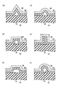
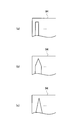
- the power module semiconductor device which concerns on 4th Embodiment, it is typical sectional structure of the stress relaxation structure part, Comprising: (a) Triangular structure example, (b) Rectangular structure example, (c) Trapezoid structure example, (d ) Semicircular structure example, (e) Another rectangular structure example, (f) Another semicircular structure example.
- FIG. 37 is a schematic sectional view taken along line VI-VI in FIG. 36.
- the typical plane pattern block diagram of the power module semiconductor device which concerns on the modification 3 of 5th Embodiment.
- the typical bird's-eye view structure figure of the columnar electrode structure part of the power module semiconductor device which concerns on a comparative example.
- the typical bird's-eye view structure figure of the power module semiconductor device which concerns on a comparative example.
- the typical bird's-eye view structure figure of the power module semiconductor device which concerns on 6th Embodiment.
- the typical bird's-eye view structure figure of the power module semiconductor device which concerns on the modification of 6th Embodiment. It is a typical plane pattern structure of the metal plate applied to the power module semiconductor device which concerns on 6th Embodiment and its modification, Comprising: (a) Example of rectangular slit, (b) Example of oval slit, (c ) Example of multiple circular patterns, (d) Example of another rectangular slit.
- FIG. 1 It is a typical plane pattern structure of the slit edge part of the metal plate applied to the power module semiconductor device which concerns on 6th Embodiment, Comprising: (a) Rectangular structure example, (b) Wedge type structure example, (c) Acute angle Triangular structure example.
- FIG. 1 It is a typical plane pattern structure of the slit edge part of the metal plate applied to the power module semiconductor device which concerns on 6th Embodiment, Comprising: (a) Rectangular structure example, (b) Wedge type structure example, (c) Acute angle Triangular structure example.
- 45A is a bird's-eye view structure of a heat spreader applied to a power module semiconductor device according to a seventh embodiment, in which (a) a structural example in which a high thermal conductivity metal layer is embedded in a portion on which a semiconductor device is mounted; ) A structural example in which a DBC substrate is arranged on top, (c) A structural example in which a high thermal conductivity metal layer is embedded in a portion on which a semiconductor device and terminal electrodes are mounted, (d) A high thermal conductivity metal layer in a portion on which a heat dissipation ceramic substrate is mounted.
- (E) An example of a structure in which a high thermal conductivity metal layer is embedded in a portion on which a semiconductor device is mounted and a portion far from a screw hole.
- the power module semiconductor device 1 includes a first copper plate layer 16 1 and a semiconductor device 24 disposed on the first copper plate layer 16 1.
- the power module semiconductor device 1 according to the first embodiment can radiate heat from both the back surface and the front surface of the semiconductor device 24.
- the first terminal electrode 10 is connected to the source contact CS / gate contact CG of the semiconductor device 24 via the first opening 2, and the second terminal electrode 12 is The drain contact CD of the semiconductor device 24 is connected through the second opening 3.
- the first copper plate layer 16 1 may be disposed on the second ceramic substrate 182 on which a second copper plate layer 16 2 on the back surface good.
- the power module semiconductor device 1 includes a third ceramic substrate 18 3 disposed on the second ceramic substrate 18 2 , and a third ceramic substrate 18 3 .
- a fourth ceramic substrate 18 4 disposed between the 1 and the first ceramic substrate 18, the fifth may include a ceramic substrate 18 5 disposed on the first ceramic substrate 18 1 on.
- the first to fifth ceramic substrates 18 1 to 18 5 are bonded to each other by the adhesive resin layer 20 on the laminated surface.
- an epoxy resin or a silicone resin can be applied to the adhesive resin layer 20.
- the power module semiconductor device 1 as shown in FIG. 1, the first terminal electrode 10, a protective layer disposed on the second terminal electrode 12, and a fifth ceramic substrate 18 5 on 14 may be provided.
- PPS polyphenyl sulfide
- the power module semiconductor device may include a copper alloy or copper molybdenum electrode layer 25 between the first copper plate layer 16 and the semiconductor device 24 as shown in FIG.
- the semiconductor device 24 and the first terminal electrode 10 / copper alloy or copper molybdenum electrode layer 25 are connected by a solder layer 24a, and the copper alloy or copper molybdenum electrode layer 25 and the first copper plate layer 16 are connected by a solder layer. 25a is connected.
- 25 may be an electrode layer made of copper alloy or molybdenum (Mo).
- the first to fifth ceramic substrates 18 1 to 18 5 are made of, for example, aluminum nitride (AlN), aluminum oxide (Al 2 O 3 ), or nitride It may be formed of any of silicon (SiN). By forming with such a material, thermal conductivity can be improved.
- AlN aluminum nitride
- Al 2 O 3 aluminum oxide
- SiN silicon
- the semiconductor device 24 is configured to perform heat dissipation from both the front and back surfaces of the semiconductor device 24, so that the semiconductor device 24 can be operated at a higher power than when the heat is radiated only from the back surface. It becomes possible to lower the surface temperature by 10 ° C. or more.
- a SiC MOSFET in which the semiconductor device 24 is formed of SiC also has a structure in which heat is radiated from both sides of the semiconductor device 24 because the electrical resistance increases at a high temperature operation of 200 ° C. or higher. The loss of 24 can be reduced.
- the first to fifth ceramic substrate 18 1-18 5 By pasting in layers, it is possible to achieve high heat dissipation structure.
- the overall height of FIG. 1B can be reduced to about 3 mm, and can be reduced by about 60% compared to the conventional structure. It is.
- the power module semiconductor device it is possible to reduce the size and increase the heat dissipation by dissipating heat from both the front and back surfaces of the semiconductor device.
- the first terminal electrode 10 and the second terminal electrode 12 are bent terminal electrode tips.
- the units 0a and 12a may be provided.
- bent terminal electrode tips 10a and 12a it is possible to improve adhesion to a heat spreader described later, or to easily take out the electrodes from the first terminal electrode 10 and the second terminal electrode 12. it can.
- Such bent terminal electrode tip portions 0a and 12a can also be formed by etching the first terminal electrode 10 and the second terminal electrode 12.
- the terminal electrode inner corner portions 10c and 12c have a curved surface that is over-etched by etching processing. It is shown.
- the processing conditions such as the concentration, composition, time, and temperature of the etchant during the etching of the first terminal electrode 10 and the second terminal electrode 12, as shown in FIGS.
- the shape of the terminal electrode tip portions 0a and 12a of the second terminal electrode 12 can be processed.
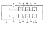
- FIG. 8 A schematic plane pattern configuration for explaining the wiring connection between the power module unit 52 and the gate drive unit 50 on which the power module semiconductor device according to the first embodiment is mounted is expressed as shown in FIG.
- power module semiconductor devices 60 1 to 60 6 for three-phase AC inverters are arranged in the power module unit 52, and the power module semiconductor devices 60 1 to 60 6 are connected to the gate drive unit 50.
- gate drive wirings 10 1 to 10 6 are connected by gate drive wirings 10 1 to 10 6 , respectively.
- FIG. 9 a schematic planar pattern configuration of the power module unit 80 in which the gate drive circuits 70 1 to 70 6 are mounted in the vicinity of the power module semiconductor devices 60 1 to 60 6 according to the first embodiment is as shown in FIG. It is expressed in In the example of FIG. 9, the gate drive circuits 70 1 to 70 6 are arranged in the vicinity of the power module semiconductor devices 60 1 to 60 6 , thereby reducing the signal delay of the gate drive signal and the power module for the three-phase AC inverter. High-frequency and high-efficiency operations of the semiconductor devices 60 1 to 60 6 can be realized.
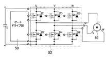
- the schematic circuit configuration of the three-phase inverter configured using the power module semiconductor device according to the first embodiment includes a gate drive unit 50 and a power module connected to the gate drive unit 50. Part 52 and a three-phase motor part 53.
- the power module unit 52 is connected to U, V, and W phase inverters corresponding to the U phase, V phase, and W phase of the three-phase motor unit 53.
- the inverter-structured SiC MOSFETs Q1 and Q2, Q3 and Q4, and Q5 and Q6 are connected between the plus terminal (+) and the minus terminal ( ⁇ ) to which the capacitor C is connected. Furthermore, diodes D1 to D6 are connected in antiparallel between the sources and drains of the SiC MOSFETs Q1 to Q6, respectively.
- the three-phase inverter configured using such a power module semiconductor device is more than when radiating heat only from the back surface.
- the temperature of the surface of the semiconductor device 24 at the time of high power operation can be lowered by 10 ° C. or more, the loss at the time of high power operation can be reduced, and further, downsizing and high efficiency are realized by thinning the layer. be able to.
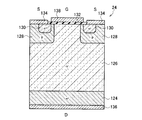
- a schematic cross-sectional structure of an SiC • MOSFET includes an n ⁇ epitaxial growth layer 126 and an n ⁇ epitaxial growth layer as shown in FIG. P base region 128 formed on the surface side of 126, source region 130 formed on the surface of p base region 128, and gate insulating film disposed on the surface of n ⁇ epitaxial growth layer 126 between p base regions 128.
- n + drain region disposed on the back surface opposite to the surface of the n ⁇ epitaxial growth layer 126 ( n + substrate) 124 and drain electrode 136 connected to n + drain region (n + substrate) 124.
- the drain electrode 136 is, for example, as shown in FIG. 3, the solder layer 24a, a copper alloy or a copper molybdenum electrode layer 25 via the solder layer 25a, and is connected to the first copper plate layer 16 1.
- a GaNFET or the like may be applied instead of the SiC • MOSFET.
- the power module semiconductor device according to the first embodiment and its modification has a double-sided cooling structure, heat dissipation is facilitated, the heat spreader is lightened, the thermal runaway of the semiconductor device is suppressed, high frequency characteristics and power consumption efficiency As a result, power conversion efficiency can be increased.
- a schematic cross-sectional structure of the power module semiconductor device 1 according to the second embodiment includes a semiconductor device 24 and a first DBC substrate (16a) disposed on the surface side of the semiconductor device 24. 18a, 16a), a second DBC substrate (16b, 18b, 16b) disposed on the back side of the semiconductor device 24, a first terminal electrode 10 connected to the first DBC substrate (16a, 18a, 16a), And a second terminal electrode 12 connected to the second DBC substrate (16b, 18b, 16b).
- the power module semiconductor device 1 according to the second embodiment can radiate heat from both the back surface and the front surface of the semiconductor device 24.
- a schematic cross-sectional structure of the DBC substrate applied to FIG. 12A includes a ceramic substrate 18 and a copper (Cu) plate layer 16 disposed on the front and back surfaces of the ceramic substrate 18.
- Cu copper
- the semiconductor device 24, the first DBC substrates (16a, 18a, 16a), the second DBC substrates (16b, 18b, 16b), and the first terminal electrodes 10 and the second terminal electrode 12 may be provided with a sealing resin layer 22.
- a sealing resin layer 22 for example, a polyimide resin, an epoxy resin, or a silicone resin can be applied to the sealing resin layer 22.
- the power module semiconductor device 1 it is possible to dissipate heat not only from the back surface but also from the front surface by bonding the DBC substrate to both the front and back sides of the semiconductor device 24.
- the surface of the semiconductor device 24 at the time of high power operation is more than that when the heat is radiated from only the back surface by adopting a structure that radiates heat from both sides of the semiconductor device 24.
- the temperature can be lowered by 10 ° C. or more.
- a SiC MOSFET in which the semiconductor device 24 is formed of SiC also has a structure in which heat is radiated from both sides of the semiconductor device 24 because the electrical resistance increases at a high temperature operation of 200 ° C. or higher. The loss of 24 can be reduced.
- the power module semiconductor device according to the second embodiment, it is possible to realize miniaturization and high heat dissipation by dissipating heat from both the front and back surfaces of the semiconductor device.
- the schematic cross-sectional structure of the power module semiconductor device 1 according to the first modification of the second embodiment is such that the second terminal electrode 12 includes a bent terminal electrode tip 12 a. good.
- a bent terminal electrode tip 12a By providing such a bent terminal electrode distal end portion 12a, it is possible to improve adhesion with a heat spreader described later, or to easily take out the electrode from the second terminal electrode 12.
- Such a bent terminal electrode tip 12a can be formed by etching the second terminal electrode 12.
- FIG. 14 a schematic planar pattern configuration of the power module semiconductor device according to the second modification of the second embodiment is expressed as shown in FIG. 14, and a schematic cross-sectional structure taken along line II-II in FIG. It is expressed as shown in FIG.
- the power module semiconductor device 1 includes a columnar electrode 48 that connects between the semiconductor device 24 and the first DBC substrate (16a, 18a, 16a). May be further provided.
- the first terminal electrode 10 is connected to the copper (Cu) plate layer 16a of the first DBC substrate (16a, 18a, 16a) at the gate contact CG / source contact CS
- the terminal electrode 12 is connected to the copper (Cu) plate layer 16b of the second DBC substrate (16b, 18b, 16b) at the drain contact CD.
- the semiconductor device 24 the first DBC substrate (16 a, 18 a, 16 a), and the second DBC substrate (16 b. 18b and 16b), the first terminal electrode 10, the second terminal electrode 12, and the sealing resin layer 22 for sealing the columnar electrode 48 may be provided.
- the schematic cross-sectional structure of the power module semiconductor device 1 according to the third modification of the second embodiment is similar to FIG. 13, and the tip of the terminal electrode in which the second terminal electrode 12 is bent.
- the part 12a may be provided.
- the power module semiconductor device according to the second embodiment and its modification has a double-sided cooling structure, heat dissipation is facilitated, the heat spreader is lightened, the thermal runaway of the semiconductor device is suppressed, high frequency characteristics and power consumption efficiency. As a result, power conversion efficiency can be increased.
- the power module semiconductor device 1 according to the third embodiment includes a first copper plate layer 16 ⁇ 16G and a semiconductor device disposed on the first copper plate layer 16 ⁇ 16G. 24, a thermally conductive insulating film 54 disposed on the semiconductor device 24, and a first terminal electrode 10 connected to the surface of the semiconductor device 24 through a first opening 2 opened in the thermally conductive insulating film 54. And the second terminal electrode 12 connected to the first copper plate layer 16 through the second opening 3 opened in the heat conductive insulating film 54.
- the power module semiconductor device 1 according to the third embodiment can radiate heat from both the back surface and the front surface of the semiconductor device 24.
- the power module semiconductor device 1 includes the first copper plate layer through the third opening 4 opened in the heat conductive insulating film 54.
- a gate terminal electrode 8 connected to the 16G surface is provided.
- the first copper plate layer 16G is connected to the gate electrode 138 of the semiconductor device 24 via the gate wiring electrode 8G.
- the first terminal electrode 10 is connected to the source contact CS / gate contact CG of the semiconductor device 24 via the first opening 2
- the second terminal electrode 12 is Via the second opening 3
- it is connected to the drain contact CD of the semiconductor device 24
- the gate terminal electrode 8 is connected via the third opening 4 to the gate contact CG on the surface of the copper plate layer 16 ⁇ / b> G.
- the entire power module semiconductor device 1 according to the third embodiment is housed in a ceramic package outer wall 56 disposed on the ceramic substrate 18.
- the ceramic package outer wall 56 disposed on the ceramic substrate 18 includes not only a side surface portion but also an upper surface portion as shown in FIG.
- the hollow portion may be filled with rare gas or nitrogen gas.
- the power module semiconductor device 1 according to the third embodiment, FIG. 17 as shown in to 19, first copper plate layer 16 1, the ceramic substrate 18 having a second copper plate layer 16 2 on the back surface It may be arranged above.
- the power module semiconductor device 1 between the first copper plate layer 16 1 and the semiconductor device 24, comprise a copper alloy or a copper molybdenum electrode layer 25 Also good. Further, while the semiconductor device 24 and the first terminal electrode 10-copper alloy or a copper molybdenum electrode layer 25 is connected by the solder layer 24a, a copper alloy or a copper molybdenum electrode layer 25 first copper plate layer 16 1 between the solder They may be connected by the layer 25a. Thus, between the first copper plate layer 16 1 and the semiconductor device 24, by placing a copper alloy or a copper molybdenum electrode layer 25, the adhesion between the semiconductor device 24 and the first copper plate layer 16 1 The heat conductivity can be improved.
- the ceramic substrate 18 is, for example, any one of aluminum nitride (AlN), aluminum oxide (Al 2 O 3 ), or silicon nitride (SiN). It may be formed. By forming with such a material, thermal conductivity can be improved.
- the first terminal electrode 10 and the second terminal electrode 12 are bent terminal electrodes as in FIG. 4 to FIG. 7 or FIG. 13 and FIG. You may provide the front-end
- a polyimide film can be applied as the heat conductive insulating film 54.
- a polyimide film can be formed by thermocompression bonding.
- the thickness of a polyimide film is about 50 micrometers, for example.
- the thickness of the power module semiconductor device according to the third embodiment since it is sufficient only in a polyimide film, the thickness of the power module semiconductor device according to the third embodiment, the thickness of the first copper plate layer 16 1 of the Cu plate for substantially radiator Contributes to the main thickness. For this reason, the overall thickness of the power module semiconductor device according to the third embodiment can be formed relatively thin.
- the thickness of the second copper plate layer 16 3 is, for example, about 50 ⁇ m to 2 mm.
- the semiconductor device 24 is configured to radiate heat from both sides of the semiconductor device 24, so that the semiconductor is operated at higher power than when radiated only from the back side.
- the temperature of the surface of the device 24 can be lowered by 10 ° C. or more.
- a SiC MOSFET in which the semiconductor device 24 is formed of SiC also has a structure in which heat is radiated from both sides of the semiconductor device 24 because the electrical resistance increases at a high temperature operation of 200 ° C. or higher. The loss of 24 can be reduced.
- the power module semiconductor device 1 according to the third embodiment and its modification, it is possible to realize miniaturization and high heat dissipation by dissipating heat from both the front and back surfaces of the semiconductor device.
- the power module semiconductor device according to the third embodiment and its modification has a double-sided cooling structure, heat dissipation is facilitated, the heat spreader is reduced in weight, the thermal runaway of the semiconductor device is suppressed, high frequency characteristics and power consumption efficiency As a result, power conversion efficiency can be increased.
- FIG. 21 a schematic planar pattern configuration of the heat conductive insulating film 54 is expressed as shown in FIG. .
- semiconductor devices 24 1 - 24 4 constituting an inverter, 24 2, 24 5, 24 3, 24 6 over with an opening 56a, the opening 58 is provided for the first copper plate layer 16 1 ing.
- FIG. 1 A schematic planar pattern configuration of the heat conductive insulating film 54 in the vicinity of the semiconductor device 24 of the power module semiconductor device according to the third embodiment and its modification is expressed as shown in FIG.
- a schematic cross-sectional structure along line IV is expressed as shown in FIG.
- the thermally conductive insulating film 54 has a deletion portion 54a formed in a corner portion C covering the semiconductor device 24 as shown in FIG. May be.
- the deleted portion 54a in the corner portion C covering the semiconductor device 24
- the step coverage of the thermally conductive insulating film 54 covering the corner portion B of the semiconductor device 24 shown in FIG. 23 is improved.
- the semiconductor device 24 and the first copper plate layer 16 1 between the example that is connected by a solder layer 24a is illustrated.
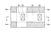
- FIG. 24 a schematic planar pattern configuration example of the thermally conductive insulating film 54 in the vicinity of the wiring portions of the semiconductor device 24 and the second terminal electrode 12 is shown in FIG.
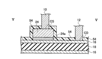
- a schematic cross-sectional structure taken along line VV of FIG. 24 is expressed as shown in FIG.
- a deletion portion 54a is formed in a corner portion covering the semiconductor device 24, and the semiconductor device 24 shown in FIG.
- the step coverage of the thermally conductive insulating film 54 covering the corners is improved.
- the source contact CS on the surface of the semiconductor device 24 and the first terminal electrode 10 are connected through the first opening 2 opened in the heat conductive insulating film 54
- the drain contact CD on the first copper plate layer 16 and the second terminal electrode 12 are connected through the second opening 3 opened in the heat conductive insulating film 54.
- FIG. 26 Another schematic plane pattern configuration of the heat conductive insulating film 54 in the vicinity of the semiconductor device 24 of the power module semiconductor device according to the third embodiment and its modification is expressed as shown in FIG.
- the deletion unit 54b of FIG. 26 has a smaller area of the deletion unit 54b than the deletion unit 54a of FIG.
- the thermally conductive insulating film 54 is shown in FIG. 23 by forming a deletion portion 54b in a corner portion covering the semiconductor device 24.
- the step coverage of the heat conductive insulating film 54 covering the corner B of the semiconductor device 24 can be improved.
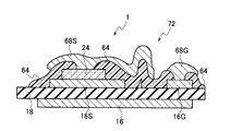
- the power module semiconductor device 1 includes a first copper plate layer 16S and 16G, a semiconductor device 24 disposed on the first copper plate layer 16S, and a semiconductor device.
- a thermally conductive insulating film 64 disposed on the semiconductor device 24; a second copper plate layer 68S connected to the surface of the semiconductor device 24 through a first opening opened in the thermally conductive insulating film 64; And a second copper plate layer 68G connected to the first copper plate layer 16G through a second opening opened in the insulating film 64.
- the first copper plate layers 16S and 16G are arranged on the ceramic substrate 18 having the third copper plate layer 16 on the back surface. May be.
- the power module semiconductor device 1 according to the fourth embodiment can radiate heat from both the back surface and the front surface of the semiconductor device 24.
- the enlarged structure of the stress relaxation structure portion of FIG. 27 is expressed as shown in FIG. 28, and has a convex heat conductive insulating film 64 and copper laminated on the convex heat conductive insulating film 64.
- a gap 74 is provided between the ceramic substrate 18 and the convex heat conductive insulating film 64.
- the power module semiconductor device 1 includes second copper plate layers 68S and 68G on a heat conductive insulating film 64 as shown in FIG.
- the power module semiconductor device 1 applies thermal stress to a part of the laminated structure of the heat conductive insulating film 64 and the second copper plate layer 68S.
- a stress relaxation structure 72 for relaxing is provided.
- the stress relaxation structure 72 is formed to be stretched by warping of the ceramic substrate 18 due to thermal stress, as shown in FIG.
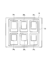
- FIG. 30 A schematic planar pattern configuration for explaining an arrangement pattern, which is an arrangement example in which the power module semiconductor device according to the fourth embodiment is applied to a three-phase inverter, is expressed as shown in FIG.
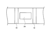
- the stress relaxation structure 72 is disposed on the ceramic substrate 18 so as to surround the semiconductor devices 24 1 , 24 4 , 24 2 , 24 5 , 24 3 , 24 6 constituting the inverter. .
- FIG. 31 a schematic planar pattern configuration in a state where thermal stress is applied in FIG. 31 is expressed as shown in FIG.
- the stress relaxation structure 72 is stretched in a direction perpendicular to the stretched direction due to warping of the ceramic substrate 18, as shown in FIGS. It may be arranged.
- FIG. 33A an example of a triangular structure is represented as shown in FIG. 33A
- FIG. (B) an example of a rectangular structure is shown in FIG. (B)
- a trapezoidal structure example is represented as shown in FIG. 33 (c)
- a semicircular structure example is represented as shown in FIG. 33 (d)
- another rectangular structure example Is represented as shown in FIG. 33 (e)
- another semicircular structure example is represented as shown in FIG. 33 (f).
- the stress relaxation structure 72 has a cross section in a direction in which the stress relaxation structure 72 is stretched due to warping of the ceramic substrate 18.
- a pattern based on any one of a triangle, a rectangle, a semicircle, and a trapezoid may be provided.
- the heat conductive insulating film 64 and the second copper plate layer 68S are formed on the surface of the semiconductor device 24, and the heat conduction is performed on the surface of the ceramic substrate 18.
- the stress relaxation structure composed of the conductive insulating film 64 and the second copper plate layer 68S is formed, and the ceramic substrate 18 having the first copper plate layer 16S on the back surface of the semiconductor device 24 and the third copper plate layer 16 on the back surface is formed. Therefore, it is possible to dissipate heat not only from the back surface but also from the front surface.
- the surface of the semiconductor device 24 at the time of high power operation is more than that when the heat is radiated from only the back surface by adopting a structure that radiates heat from both sides of the semiconductor device 24.
- the temperature can be lowered by 10 ° C. or more.
- a SiC MOSFET in which the semiconductor device 24 is formed of SiC also has a structure in which heat is radiated from both sides of the semiconductor device 24 because the electrical resistance increases at a high temperature operation of 200 ° C. or higher. The loss of 24 can be reduced.
- the stress associated with the warpage of the ceramic substrate can be relaxed and the occurrence of cracks can be suppressed by the stress relaxation structure.
- the power module semiconductor device according to the fourth embodiment, it is possible to realize miniaturization and high heat dissipation by dissipating heat from both the front and back surfaces of the semiconductor device 24.
- the power module semiconductor device according to the fourth embodiment, it is possible to realize miniaturization and high heat dissipation by dissipating heat from both the front and back surfaces of the semiconductor device.
- the power module semiconductor device has a double-sided cooling structure, heat dissipation is facilitated, the heat spreader is reduced in weight, the thermal runaway of the semiconductor device is suppressed, the high frequency characteristics and the power consumption efficiency are improved. As a result, power conversion efficiency can be increased.
- the power module semiconductor device 1 includes a first copper plate layer 16 1 and a semiconductor device 24 disposed on the first copper plate layer 16 1 (16D).
- a first ceramic substrate 18 1 disposed on the semiconductor device 24; a first terminal electrode 10 connected to the surface of the semiconductor device 24 through a first opening opened in the first ceramic substrate 18 1 ;
- a gate drive integrated circuit 76 which is disposed on the ceramic substrate 18 1 and drives the semiconductor device 24.
- the power module semiconductor device 1 according to the fifth embodiment can radiate heat from both the back surface and the front surface of the semiconductor device 24.
- the first copper plate layer 16 1 may be disposed on the second ceramic substrate 182 on which a second copper plate layer 16 2 on the back surface good.
- the first terminal electrode 10 is connected to a first copper plate layer 16 1 (16S) disposed on the second ceramic substrate 18 2 .
- the power module semiconductor device 1 includes a third ceramic substrate 18 3 disposed on the second ceramic substrate 18 2 and a third ceramic substrate 18 3 .
- a fourth ceramic substrate 18 4 disposed between the first ceramic substrate 18 1, a fifth ceramic substrate 18 5 disposed on the first ceramic substrate 181 on the sealing on the gate driver integrated circuit 76 6 may be provided with a ceramic substrate 18 6 arranged through the resin layer 22.
- the semiconductor device 24 and the gate drive integrated circuit 76 are connected via the gate terminal electrode 8, and the gate drive integrated circuit 76 is further connected with the gate terminal electrode 8I.
- the power module semiconductor device 1 as shown in FIG. 34, the first terminal electrode 10, the gate terminal electrode 8 is disposed on the sixth ceramic substrate 18 6 and the gate on the terminal electrode 8I and a seventh ceramic substrate 18 7, it may be provided with a protective layer 14 disposed on the seventh ceramic substrate 18 7.
- PPS polyphenyl sulfide
- the first to seventh ceramic substrates 18 1 to 18 5 are bonded to each other with the adhesive resin layer 20 on the laminated surface.
- an epoxy resin or a silicone resin can be applied to the adhesive resin layer 20.
- a ceramic substrate is formed in a layered manner on the semiconductor device 24, and the gate drive integrated circuit 76 is mounted therein, whereby the semiconductor device 24 and the gate are mounted. Since the drive integrated circuits 76 can be arranged close to each other, it is possible to suppress noise from being superimposed on the gate driving wiring.
- the gate drive integrated circuit is also provided in the power module semiconductor device by incorporating the copper plate layer and the semiconductor device between the ceramic substrates stacked in layers.
- the power module semiconductor device can be miniaturized.
- the power module semiconductor device 1 according to the first modification of the fifth embodiment is formed on the first copper plate layer 16 1 (16D) and the first copper plate layer 16 1 (16D).
- the electrode 10 and a gate drive integrated circuit 76 disposed on the thermally conductive insulating film 54 are provided.
- the power module semiconductor device 1 according to the first modification of the fifth embodiment can radiate heat from both the back surface and the front surface of the semiconductor device 24.
- the first terminal electrode 10 is connected to a first copper plate layer 16 1 (16S) disposed on the ceramic substrate 18 1 .
- the semiconductor device 24 and the gate drive integrated circuit 76 are connected via the gate terminal electrode 8, and the gate drive integrated circuit 76 is further connected with the gate terminal electrode 8I.
- the heat conductive insulating film is formed on the semiconductor device 24, and the gate drive integrated circuit 76 is mounted on the heat conductive insulating film.
- the semiconductor device 24 and the gate drive integrated circuit 76 can be arranged close to each other, it is possible to suppress noise from being superimposed on the gate driving wiring.
- a heat conductive insulating film is formed on the semiconductor device 24, and a gate drive is built in by incorporating a copper plate layer and a semiconductor device.
- the integrated circuit can also be incorporated in the power module semiconductor device, and the power module semiconductor device can be miniaturized.
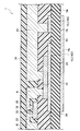
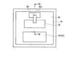
- FIG. 36 A schematic plane pattern configuration of the power module semiconductor device according to the second modification of the fifth embodiment is expressed as shown in FIG. 36, and a schematic cross-sectional structure taken along line VI-VI in FIG. 36 is shown in FIG. It is expressed as shown in
- the power module semiconductor device includes a first copper plate layer 16D and a semiconductor device 24 arranged on the first copper plate layer 16D.
- a thermally conductive insulating film 54 disposed on the semiconductor device 24; a gate drive integrated circuit 76 disposed on the thermally conductive insulating film 54; and a first terminal electrode 10 (CS) connected to the surface of the semiconductor device 24.
- CS first terminal electrode 10
- a gate wiring electrode 8G, and a gate wiring electrode 82 for connecting the gate drive integrated circuit 76 and the gate wiring electrode 8G.
- the power module semiconductor device 1 according to the second modification of the fifth embodiment can radiate heat from both the back surface and the front surface of the semiconductor device 24.
- the gate drive integrated circuit is also powered by disposing the gate drive integrated circuit 76 on the semiconductor device 24 via the heat conductive insulating film.
- the module can be built in the module semiconductor device, and the power module semiconductor device can be downsized.
- the direction of the signal current IGL flowing through the gate wiring electrode 82 is opposite to the direction of the current IGT flowing through the semiconductor device 24. Therefore, the inductance component accompanying the gate wiring electrode 82 can be canceled out.
- a schematic planar pattern configuration of a power module semiconductor device according to Modification 3 of the fifth embodiment is expressed as shown in FIG.
- the gate wiring electrode 8G connected to the surface of the semiconductor device 24 and the gate wiring electrode connecting the gate drive integrated circuit 76 and the gate wiring electrode 8G.
- the pattern layout of 82 is different, other configurations are the same as those of the power module semiconductor device according to the third modification.
- the gate drive integrated circuit and the power module are arranged on the semiconductor device 24 through the heat conductive insulating film.
- the power module semiconductor device can be miniaturized because it can be built in the semiconductor device.
- the direction of the signal current I GL flowing through the gate wiring electrode 82, the direction of the current I GT flowing semiconductor device 24 is reversed Therefore, the inductance component accompanying the gate wiring electrode 82 can be canceled out.
- a schematic bird's-eye view structure of the columnar electrode structure portion of the power module semiconductor device according to the comparative example includes a ceramic substrate 18, a semiconductor device 24 arranged on the ceramic substrate 18, and a semiconductor device 24, as shown in FIG.
- a columnar electrode 90 disposed and a metal plate 92 disposed on the columnar electrode 90 are provided.
- a schematic bird's-eye view structure of the power module semiconductor device according to the comparative example includes a heat spreader 100, a ceramic substrate 18 disposed on the heat spreader 100, and a semiconductor device disposed on the ceramic substrate 18, as shown in FIG. 24 1 , 24 2 , 24 3 , columnar electrodes 90 1 , 90 2 , 90 3 disposed on the semiconductor devices 24 1 , 24 2 , 24 3 , and columnar electrodes 90 1 , 90 2 , 90 3
- the metal plate 92 is provided.
- the power module semiconductor device improves the module performance both electrically and thermally by using the columnar electrode.
- the heat spreader 100 warp direction A + -A + / A--A- and the metal plate 92 warp direction C + -C + / C--C- Since they are orthogonal, the yield decreases.
- a schematic bird's-eye view structure of the power module semiconductor device 1 according to the sixth embodiment is disposed on the heat spreader 100, the ceramic substrate 18 disposed on the heat spreader 100, and the ceramic substrate 18.
- a metal plate 94 disposed thereon.
- the metal plate 94 includes a slit structure as shown in FIG.
- the power module semiconductor device 1 according to the sixth embodiment can radiate heat from both the back surface and the front surface of the semiconductor device 24.
- a schematic bird's-eye view structure of the power module semiconductor device 1 according to the sixth embodiment includes a warp direction A + ⁇ A + / A ⁇ A ⁇ and a metal plate having a slit structure. Since the warpage direction B + ⁇ B + / B ⁇ B ⁇ of 94 is made parallel, the yield is improved. Further, by using the columnar electrodes 90 1 , 90 2 , 90 3 , module performance is improved both electrically and thermally.
- the shape of the metal plate on the column is matched with the shape of the heat spreader. Therefore, mechanical stress can be suppressed and the occurrence of cracks in the metal joint can be suppressed.
- the warp of the metal material when the temperature of the module rises and falls generates stress in the metal joint portion.
- the stress can be reduced, the stress generated during cooling after metal bonding can be suppressed, and the assembly yield can be increased.
- the assembly yield when the direction of the warp between the heat spreader 100 and the metal plate 94 on the column is not matched is 5% out of 18 modules, which is about 28%, but the heat spreader 100 and the metal plate 94 on the column are about 28%.
- the assembly yield when the directions of warpage are matched is 18% out of 18 modules, which is 100%.
- warping of the heat spreader and the metal plate on the pillar is made by making the longitudinal directions of the heat spreader 100 and the metal plate 94 on the pillar the same direction. Can be aligned.
- a schematic bird's-eye view structure of the power module semiconductor device 1 according to the modification of the sixth embodiment includes a DBC substrate (16, 18, 16) and a DBC substrate (16, 18, 16).
- a columnar electrode 90 disposed and a metal plate 94 having a slit structure disposed on the columnar electrode 90 are provided.
- the power module semiconductor device 1 according to the modification of the sixth embodiment can radiate heat from both the back surface and the front surface of the semiconductor device 24.
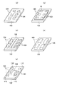
- FIG. 43 (a) A schematic planar pattern configuration of the metal plate 94 applicable to the power module semiconductor device according to the sixth embodiment and its modification, and an example having a rectangular slit is shown in FIG. 43 (a).
- An example having an oval slit is represented as shown in FIG. 43 (b)
- an example having a plurality of circular patterns is represented as shown in FIG. 43 (c)
- an example having another rectangular slit is shown in FIG.
- FIG. 44A shows a schematic planar pattern configuration of the slit end portion of the metal plate 94 applicable to the power module semiconductor device according to the sixth embodiment and its modification.
- An example of a wedge-shaped structure is represented as shown in FIG. 44 (b)
- an example of an acute angle triangular structure is represented as shown in FIG. 44 (c).
- the slit shape may be any one of a comb shape, a rectangle shape, and a circular dot arrangement along the longitudinal direction of the heat spreader.
- the slit shape has a comb shape or a rectangle along the longitudinal direction of the heat spreader, and the end portion of the slit shape has a curved shape, a rectangle or a triangle. You may have.
- the heat radiation performance can be further improved by applying the columnar electrode and the metal plate.
- the power module semiconductor device According to the sixth embodiment and the modification thereof, it is possible to realize miniaturization and high heat dissipation by dissipating heat from both the front and back surfaces of the semiconductor device.
- the power module semiconductor device according to the sixth embodiment and its modification has a double-sided cooling structure, heat dissipation is facilitated, the heat spreader is reduced in weight, the thermal runaway of the semiconductor device is suppressed, high-frequency characteristics, and power consumption efficiency As a result, power conversion efficiency can be increased.
- FIG. 45A shows a bird's eye view structure of a heat spreader applied to a power module semiconductor device according to the seventh embodiment, in which a high thermal conductivity metal layer is embedded in a portion where a semiconductor device is mounted.
- An example of a structure in which a DBC substrate is arranged on FIG. 45A is represented as shown in FIG.
- FIG. 45 (c) shows a bird's eye view structure of a heat spreader applied to the power module semiconductor device according to the seventh embodiment, in which a high thermal conductivity metal layer is embedded in a portion where a semiconductor device and terminal electrodes are mounted.
- An example of a structure in which a high thermal conductivity metal layer is embedded in a portion where a heat dissipation ceramic substrate is mounted is represented as shown in FIG.
- FIG. 45 (e) a bird's eye view structure of a heat spreader applied to the power module semiconductor device according to the seventh embodiment, and a structure example in which a high thermal conductivity metal layer is embedded in a portion mounting a semiconductor device and a portion far from a screw hole is shown in FIG. 45 (e).
- the heat spreader 102 has a structure in which the high thermal conductivity metal layer 104 is embedded in the portion where the semiconductor device 24 is mounted, as shown in FIG. May be.
- a DBC substrate (18 / 16D) may be further provided on the heat spreader 102 as shown in FIG.
- the heat spreader 102 further includes a portion on which the first terminal electrode 10 and the second terminal electrode 12 are mounted.
- a structure in which the high thermal conductivity metal layer 105 is embedded may be provided.
- the heat spreader 102 has a structure in which the high thermal conductivity metal layer 106 is embedded in the portion where the ceramic substrate 18 is mounted, as shown in FIG. You may have.
- the heat spreader 102 has a high thermal conductivity in a portion where the semiconductor device 24 is mounted and a portion far from the screw hole 110 formed for fixing the heat spreader 102.
- a structure in which the metal layers 104 and 108 are embedded may be provided.
- the heat spreader 102 may be formed of CuMo, and the high thermal conductivity metal layers 104, 105, 106, and 108 may be formed of Cu.
- a heat spreader with low stress and high heat dissipation can be formed, and a heat spreader with high heat dissipation and less warpage can be formed. it can.
- the heat spreader 102 is formed under the semiconductor device 24 with high thermal conductivity copper, and the other heat spreader has a low linear thermal expansion coefficient such as CuMo.
- the heat spreader 102 is formed under the semiconductor device 24 with high thermal conductivity copper, and the other heat spreader has a low linear thermal expansion coefficient such as CuMo.
- the temperature of the semiconductor device during high power operation is 10 ° C. or higher. Can be lowered. Further, by using a material having a low coefficient of linear thermal expansion such as CuMo, it is possible to reduce the stress of the metal joint portion under the semiconductor device by 10% or more.
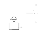
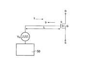
- the circuit configuration for explaining the high-frequency drive includes a gate drive unit 50 and a gate drive signal V G supplied from the gate drive unit 50. And a supplied semiconductor device Q.
- the circuit configuration for explaining the high frequency driving in consideration of the reflected wave Ir is supplied from the gate drive unit 50 and the gate drive unit 50 as shown in FIG.
- the semiconductor device Q is supplied with the gate drive signal V G, and the wiring length L of the metal wiring from the gate drive unit 50 to the semiconductor device Q is an odd multiple of the half wavelength of the gate drive signal wavelength.
- the gate electrode of the semiconductor device Q is made of a metal material.
- a semiconductor device Q when high-frequency driving, when the input from the gate drive unit 50 of the gate drive signal V G to the semiconductor device Q, incident wave Ii to semiconductor devices Q When, as reflected wave Ir reflected from the semiconductor device Q is not Awa weaken, and the gate drive signal V wiring length of an odd multiple of the half wavelength of G L.
- the operating frequency is sufficiently smaller than the frequency band corresponding to the switching time, so there is no significant influence on the characteristics.
- the operating frequency exceeds, for example, 10 MHz, the switching time cannot be ignored and the influence of the reflected wave of the input signal comes out.
- the gate electrode of the semiconductor device Q When driving at low frequency, the gate electrode of the semiconductor device Q does not have a significant effect on the characteristics even if polysilicon with a sheet resistance of about several hundred m ⁇ / ⁇ to about several ⁇ / ⁇ is used. In driving, it is necessary to form the gate electrode with a metal electrode in order to lower the input impedance to the gate, which makes it possible to increase the operating frequency to several MHz.
- the efficiency is increased by driving at a high frequency, or parts to be used can be downsized.
- high-frequency driving when the input from the gate drive unit 50 of the gate drive signal V G to the semiconductor device Q, the incident wave Ii to semiconductor devices Q, so that the reflected wave Ir does Awa weaken reflected from the semiconductor device Q
- the wiring length L is an odd multiple of the half wavelength of the gate drive signal V G.
- the gate drive signal input to the power module is configured such that the wiring length L from the gate drive unit 50 to the semiconductor device Q is set to an odd multiple of the half wavelength of the drive frequency. Cancellation can be eliminated.
- the wiring length from the gate drive unit 50 to the gate oxide film of the semiconductor device Q is preferably an odd multiple of a half wavelength of the drive frequency.
- the semiconductor device Q is one of Si, SiC, or a GaN-based semiconductor.
- the gate drive signal input to the power module is controlled by the wiring length L from the gate drive unit 50 to the semiconductor device Q during the control of driving a plurality of chips in phase. It is particularly effective to eliminate the cancellation of the incident wave and the reflected wave by setting the length to an odd multiple of the half wavelength.
- a configuration example in which the back surface 96b is roughened is expressed as shown in FIG.
- both the front surface 96a and the back surface 96b of the metal wiring 96 are roughened to improve the adhesion with peripheral materials, and at the front surface 96a and the back surface 96b of the metal wiring 96, Signal transmission speed can be adjusted and matched.
- a power module semiconductor device having excellent heat dissipation characteristics can be provided.
- the semiconductor device of the present invention can be applied to all power devices such as electric semiconductors, hybrid vehicles, industrial equipment, inverters, power semiconductor modules mounted on home appliances, intelligent power modules, and the like.
Landscapes
- Cooling Or The Like Of Semiconductors Or Solid State Devices (AREA)
Abstract
放熱特性に優れたパワーモジュール半導体装置を提供する。パワーモジュール半導体装置は、第1銅プレート層16と、第1銅プレート層16上に配置された半導体デバイス24と、半導体デバイス24上に配置された第1セラミック基板18と、第1セラミック基板18に開口された第1開口部を介して半導体デバイス24表面に接続された第1端子電極10と、第1セラミック基板18に開口された第2開口部を介して第1銅プレート層16に接続された第2端子電極12とを備え、半導体デバイス24の裏面と表面の両面から放熱を行う。
Description
本発明は、パワーモジュール半導体装置に関し、特に、放熱特性を改善したパワーモジュール半導体装置に関する。
現在多くの研究機関において、シリコンカーバイド(SiC:Silicon Carbide)デバイスの研究開発が行われている。SiCデバイスの特徴として、低オン抵抗、高速スイッチングおよび高温動作などを挙げることができる。
従来、半導体パワーモジュールの分野で使用されている絶縁ゲートバイポーラトランジスタ(IGBT:Insulated Gate Bipolar Transistor)などのSiデバイスでは、動作可能な温度範囲が150℃程度までであるため、従来のSn-Ag系などの低融点半田を使用しても駆動することが可能であった。
しかしながら、SiCデバイスでは、理論的に、約400℃まで動作可能であり、従来の低融点半田を使用する場合、SiCデバイスを高温で駆動すると、低融点半田による結合部が溶融し、電極間のショート、SiCデバイスとベースプレート間の剥離などを生じ、SiCデバイスの信頼性を損なうものとなっていた。
このため、SiCデバイスを高温で駆動することができず、SiCデバイスの特徴を最大限に生かすことができなかった。
SiCデバイスの相互接続方法および低熱抵抗パッケージについては、既に開示されている(例えば、特許文献1および特許文献2参照。)。特許文献1および特許文献2においては、SiCデバイスを収容するパッケージの形成方法が開示されており、SiCデバイスは、他の部品若しくは導電性表面に対して、TLP接合技術を用いて結合されている。
また、半導体素子を裏面から冷却器を介して液体冷却する機器についても開示されている(例えば、特許文献3参照。)。
本発明の目的は、放熱特性に優れたパワーモジュール半導体装置を提供することにある。
上記目的を達成するための本発明の一態様によれば、第1銅プレート層と、前記第1銅プレート層上に配置された半導体デバイスと、前記半導体デバイス上に配置された第1セラミック基板と、前記第1セラミック基板に開口された第1開口部を介して前記半導体デバイス表面に接続された第1端子電極と、前記第1セラミック基板に開口された第2開口部を介して前記第1銅プレート層に接続された第2端子電極とを備え、前記半導体デバイスの裏面と表面の両面から放熱を行うパワーモジュール半導体装置が提供される。
本発明の別の態様によれば、半導体デバイスと、前記半導体デバイスの表面側に配置された第1DBC基板と、前記半導体デバイスの裏面側に配置された第2DBC基板と、前記第1DBC基板に接続された第1端子電極と、前記第2DBC基板に接続された第2端子電極とを備え、前記半導体デバイスの裏面と表面の両面から放熱を行うパワーモジュール半導体装置が提供される。
本発明のさらに別の態様によれば、第1銅プレート層と、前記第1銅プレート層上に配置された半導体デバイスと、前記半導体デバイス上に配置された熱伝導性絶縁フィルムと、前記熱伝導性絶縁フィルムに開口された第1開口部を介して前記半導体デバイス表面に接続された第1端子電極と、前記熱伝導性絶縁フィルムに開口された第2開口部を介して前記第1銅プレート層に接続された第2端子電極とを備え、前記半導体デバイスの裏面と表面の両面から放熱を行うパワーモジュール半導体装置が提供される。
本発明によれば、放熱特性に優れたパワーモジュール半導体装置を提供することができる。
次に、図面を参照して、本発明の実施の形態を説明する。以下の図面の記載において、同一又は類似の部分には同一又は類似の符号を付している。ただし、図面は模式的なものであり、厚みと平面寸法との関係、各層の厚みの比率等は現実のものとは異なることに留意すべきである。したがって、具体的な厚みや寸法は以下の説明を参酌して判断すべきものである。又、図面相互間においても互いの寸法の関係や比率が異なる部分が含まれていることはもちろんである。
又、以下に示す実施の形態は、この発明の技術的思想を具体化するための装置や方法を例示するものであって、この発明の実施の形態は、構成部品の材質、形状、構造、配置等を下記のものに特定するものでない。この発明の実施の形態は、特許請求の範囲において、種々の変更を加えることができる。
[第1の実施の形態]
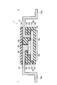
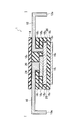
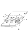
第1の実施の形態に係るパワーモジュール半導体装置1は、図1~図3に示すように、第1銅プレート層161と、第1銅プレート層161上に配置された半導体デバイス24と、半導体デバイス24上に配置された第1セラミック基板181と、第1セラミック基板181に開口された第1開口部2を介して半導体デバイス24表面に接続された第1端子電極10と、第1セラミック基板181に開口された第2開口部3を介して第1銅プレート層161に接続された第2端子電極12とを備える。ここで、第1の実施の形態に係るパワーモジュール半導体装置1は、半導体デバイス24の裏面と表面の両面から放熱を行うことができる。
第1の実施の形態に係るパワーモジュール半導体装置1は、図1~図3に示すように、第1銅プレート層161と、第1銅プレート層161上に配置された半導体デバイス24と、半導体デバイス24上に配置された第1セラミック基板181と、第1セラミック基板181に開口された第1開口部2を介して半導体デバイス24表面に接続された第1端子電極10と、第1セラミック基板181に開口された第2開口部3を介して第1銅プレート層161に接続された第2端子電極12とを備える。ここで、第1の実施の形態に係るパワーモジュール半導体装置1は、半導体デバイス24の裏面と表面の両面から放熱を行うことができる。
図1~図3に示すように、例えば、第1端子電極10は、第1開口部2を介して、半導体デバイス24のソースコンタクトCS/ゲートコンタクトCGに接続され、第2端子電極12は、第2開口部3を介して、半導体デバイス24のドレインコンタクトCDに接続される。
また、第1の実施の形態に係るパワーモジュール半導体装置1において、第1銅プレート層161は、裏面に第2銅プレート層162を有する第2セラミック基板182上に配置されていても良い。
また、第1の実施の形態に係るパワーモジュール半導体装置1は、図1に示すように、第2セラミック基板182上に配置された第3セラミック基板183と、第3セラミック基板183上、第1セラミック基板181との間に配置された第4セラミック基板184と、第1セラミック基板181上に配置された第5セラミック基板185とを備えていても良い。ここで、第1~第5セラミック基板181~185は、積層面において互いに接着樹脂層20で接着されている。ここで、接着樹脂層20には、例えば、エポキシ系樹脂もしくはシリコーン系樹脂などを適用することができる。
また、第1の実施の形態に係るパワーモジュール半導体装置1は、図1に示すように、第1端子電極10、第2端子電極12、および第5セラミック基板185上に配置された保護層14を備えていても良い。ここで、保護層14には、例えば、PPS(ポリフェニルサルファイド)などを適用することができる。
第1の実施の形態に係るパワーモジュール半導体装置は、図3に示すように、第1銅プレート層16と半導体デバイス24間には、銅合金または銅モリブデン電極層25を備えていても良い。また、半導体デバイス24と第1端子電極10・銅合金または銅モリブデン電極層25間は、半田層24aによって接続され、銅合金または銅モリブデン電極層25と第1銅プレート層16間は、半田層25aによって接続されている。このように、第1銅プレート層16と半導体デバイス24間に、銅合金または銅モリブデン電極層25を配置することによって、半導体デバイス24と第1銅プレート層16との間の密着性を向上し、熱伝導性を良好にすることができる。25は、銅合金またはモリブデン(Mo)からなる電極層であっても良い。
また、第1の実施の形態に係るパワーモジュール半導体装置において、第1~第5セラミック基板181~185は、例えば、窒化アルミニウム(AlN)、酸化アルミニウム(Al2O3、)、若しくは窒化シリコン(SiN)のいずれかで形成されていても良い。このような材料で形成することによって、熱伝導性を良好にすることができる。
第1の実施の形態に係るパワーモジュール半導体装置においては、半導体デバイス24表面・裏面の両面から放熱を行う構造とすることで、裏面のみから放熱する時よりも、大電力動作時の半導体デバイス24表面の温度を10℃以上下げることが可能となる。
例えば、半導体デバイス24をSiCで形成したSiCMOSFETにおいても200℃以上の高温動作では、電気抵抗が上昇するため、半導体デバイス24の両面から放熱を行う構造とすることで、大電力動作時の半導体デバイス24の損失を低減することができる。
第1の実施の形態に係るパワーモジュール半導体装置においては、第1~第5セラミック基板181~185を層状に貼り付けることで、高放熱性の構造を実現することができる。
第1の実施の形態に係るパワーモジュール半導体装置においては、図1(b)の全体の高さは、3mm程度と薄くすることができ、従来構造に比較して、約60%薄層化可能である。
第1の実施の形態に係るパワーモジュール半導体装置においては、半導体デバイスの表裏両面から放熱することにより、小型化、高放熱化を実現することができる。
(変形例)
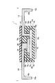
第1の実施の形態の変形例1~4に係るパワーモジュール半導体装置1においては、図4~図7に示すように、第1端子電極10・第2端子電極12は、屈曲した端子電極先端部0a・12aを備えていても良い。このような屈曲した端子電極先端部10a・12aを備えることによって、後述するヒートスプレッダとの密着性を向上させ、或いは第1端子電極10・第2端子電極12からの電極取り出しを容易にすることができる。このような屈曲した端子電極先端部0a・12aは、第1端子電極10・第2端子電極12をエッチング加工することによっても形成することができる。
第1の実施の形態の変形例1~4に係るパワーモジュール半導体装置1においては、図4~図7に示すように、第1端子電極10・第2端子電極12は、屈曲した端子電極先端部0a・12aを備えていても良い。このような屈曲した端子電極先端部10a・12aを備えることによって、後述するヒートスプレッダとの密着性を向上させ、或いは第1端子電極10・第2端子電極12からの電極取り出しを容易にすることができる。このような屈曲した端子電極先端部0a・12aは、第1端子電極10・第2端子電極12をエッチング加工することによっても形成することができる。
第1の実施の形態の変形例3に係るパワーモジュール半導体装置1においては、図6に示すように、エッチング加工によって、端子電極内側コーナー部10b・12bが滑らかな曲面を有する例が示されている。
一方、第1の実施の形態の変形例4に係るパワーモジュール半導体装置1においては、図7に示すように、エッチング加工によって、端子電極内側コーナー部10c・12cがオーバーエッチングされた曲面を有する例が示されている。第1端子電極10・第2端子電極12のエッチング時のエッチング液の濃度、配合、時間、温度などの加工条件を調整することによって、図5~図7に示すように、第1端子電極10・第2端子電極12の端子電極先端部0a・12aの形状を加工可能である。
第1の実施の形態に係るパワーモジュール半導体装置を搭載したパワーモジュール部52とゲートドライブ部50の配線接続を説明する模式的平面パターン構成は、図8に示すように表される。図8において、パワーモジュール部52には、3相交流インバータ用のパワーモジュール半導体装置601~606が配置されており、パワーモジュール半導体装置601~606は、ゲートドライブ部50との間を、それぞれゲート駆動配線101~106により接続されている。
また、第1の実施の形態に係るパワーモジュール半導体装置601~606の近傍にゲートドライブ回路701~706を搭載したパワーモジュール部80の模式的平面パターン構成は、図9に示すように表される。図9の例では、パワーモジュール半導体装置601~606の近傍にゲートドライブ回路701~706を配置することによって、ゲートドライブ信号の信号遅延を低減し、3相交流インバータ用のパワーモジュール半導体装置601~606の高周波、高効率の動作を実現可能である。
(パワーモジュールの構成)
第1の実施の形態に係るパワーモジュール半導体装置を用いて構成した3相インバータの模式的回路構成は、図10に示すように、ゲートドライブ部50と、ゲートドライブ部50に接続されたパワーモジュール部52と、3相モータ部53とを備える。パワーモジュール部52は、3相モータ部53のU相、V相、W相に対応して、U、V、W相のインバータが接続されている。
第1の実施の形態に係るパワーモジュール半導体装置を用いて構成した3相インバータの模式的回路構成は、図10に示すように、ゲートドライブ部50と、ゲートドライブ部50に接続されたパワーモジュール部52と、3相モータ部53とを備える。パワーモジュール部52は、3相モータ部53のU相、V相、W相に対応して、U、V、W相のインバータが接続されている。
パワーモジュール部52は、コンデンサCが接続されたプラス端子(+)とマイナス端子(-)間に、インバータ構成のSiC・MOSFETQ1・Q2、Q3・Q4、およびQ5・Q6が接続されている。さらに、SiC・MOSFETQ1~Q6のソース・ドレイン間には、ダイオードD1~D6がそれぞれ逆並列に接続されている。
第1の実施の形態およびその変形例に係るパワーモジュール半導体装置は、両面冷却構造を備えるため、このようなパワーモジュール半導体装置を用いて構成した3相インバータは、裏面のみから放熱する時よりも、大電力動作時の半導体デバイス24表面の温度を10℃以上下げることが可能となり、大電力動作時の損失を低減することができ、しかも薄層化により、小型化、高効率化を実現することができる。
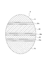
第1の実施の形態に係るパワーモジュール半導体装置に適用する半導体デバイス24の例として、SiC・MOSFETの模式的断面構造は、図11に示すように、n-エピタキシャル成長層126と、n-エピタキシャル成長層126の表面側に形成されたpベース領域128と、pベース領域128の表面に形成されたソース領域130と、pベース領域128間のn-エピタキシャル成長層126の表面上に配置されたゲート絶縁膜132と、ゲート絶縁膜132上に配置されたゲート電極138と、ソース領域130に接続されたソース電極134と、n-エピタキシャル成長層126の表面と反対側の裏面に配置されたn+ドレイン領域(n+基板)124と、n+ドレイン領域(n+基板)124に接続されたドレイン電極136とを備える。
ドレイン電極136は、例えば、図3に示すように、半田層24a、銅合金または銅モリブデン電極層25、半田層25aを介して、第1銅プレート層161に接続されている。
なお、第1の実施の形態に係るパワーモジュール半導体装置に適用する半導体デバイスの例として、SiC・MOSFETの代わりに、GaNFETなどを適用することもできる。
第1の実施の形態およびその変形例に係るパワーモジュール半導体装置は、両面冷却構造を備えるため、熱放散が容易となり、ヒートスプレッダの軽量化、半導体デバイスの熱暴走の抑制、高周波特性および消費電力効率などの性能向上をはかることができ、結果として、電力変換効率を増大することができる。
[第2の実施の形態]
第2の実施の形態に係るパワーモジュール半導体装置1の模式的断面構造は、図12(a)に示すように、半導体デバイス24と、半導体デバイス24の表面側に配置された第1DBC基板(16a・18a・16a)と、半導体デバイス24の裏面側に配置された第2DBC基板(16b・18b・16b)と、第1DBC基板(16a・18a・16a)に接続された第1端子電極10と、第2DBC基板(16b・18b・16b)に接続された第2端子電極12とを備える。ここで、第2の実施の形態に係るパワーモジュール半導体装置1は、半導体デバイス24の裏面と表面の両面から放熱を行うことができる。
第2の実施の形態に係るパワーモジュール半導体装置1の模式的断面構造は、図12(a)に示すように、半導体デバイス24と、半導体デバイス24の表面側に配置された第1DBC基板(16a・18a・16a)と、半導体デバイス24の裏面側に配置された第2DBC基板(16b・18b・16b)と、第1DBC基板(16a・18a・16a)に接続された第1端子電極10と、第2DBC基板(16b・18b・16b)に接続された第2端子電極12とを備える。ここで、第2の実施の形態に係るパワーモジュール半導体装置1は、半導体デバイス24の裏面と表面の両面から放熱を行うことができる。
図12(a)に適用するDBC基板の模式的断面構造は、図12(b)に示すように、セラミック基板18と、セラミック基板18の表面と裏面に配置された銅(Cu)プレート層16とを備える。
また、第2の実施の形態に係るパワーモジュール半導体装置1において、半導体デバイス24と、第1DBC基板(16a・18a・16a)と、第2DBC基板(16b・18b・16b)と、第1端子電極10と、第2端子電極12とを封止する封止樹脂層22を備えていても良い。ここで、封止樹脂層22は、例えば、ポリイミド系樹脂、エポキシ系樹脂、若しくはシリコーン系樹脂などを適用可能である。
第2の実施の形態に係るパワーモジュール半導体装置1においては、DBC基板を半導体デバイス24の表と裏の両側に接合することにより、裏面からだけでなく表面からも放熱することが可能になる。
第2の実施の形態に係るパワーモジュール半導体装置1においては、半導体デバイス24の両面から放熱を行う構造とすることで、裏面のみから放熱する時よりも、大電力動作時の半導体デバイス24表面の温度を10℃以上下げることが可能となる。
例えば、半導体デバイス24をSiCで形成したSiCMOSFETにおいても200℃以上の高温動作では、電気抵抗が上昇するため、半導体デバイス24の両面から放熱を行う構造とすることで、大電力動作時の半導体デバイス24の損失を低減することができる。
また、第2の実施の形態に係るパワーモジュール半導体装置においては、半導体デバイスの表裏両面から放熱することにより、小型化、高放熱化を実現することができる。
(変形例)
第2の実施の形態の変形例1に係るパワーモジュール半導体装置1の模式的断面構造は、図13に示すように、第2端子電極12は、屈曲した端子電極先端部12aを備えていても良い。このような屈曲した端子電極先端部12aを備えることによって、後述するヒートスプレッダとの密着性を向上させ、或いは第2端子電極12からの電極取り出しを容易にすることができる。このような屈曲した端子電極先端部12aは、第2端子電極12をエッチング加工することによって形成することができる。
第2の実施の形態の変形例1に係るパワーモジュール半導体装置1の模式的断面構造は、図13に示すように、第2端子電極12は、屈曲した端子電極先端部12aを備えていても良い。このような屈曲した端子電極先端部12aを備えることによって、後述するヒートスプレッダとの密着性を向上させ、或いは第2端子電極12からの電極取り出しを容易にすることができる。このような屈曲した端子電極先端部12aは、第2端子電極12をエッチング加工することによって形成することができる。
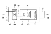
また、第2の実施の形態の変形例2に係るパワーモジュール半導体装置の模式的平面パターン構成は、図14に示すように表され、図14のII-II線に沿う模式的断面構造は、図15に示すように表される。
第2の実施の形態の変形例2に係るパワーモジュール半導体装置1は、図14および図15に示すように、半導体デバイス24と第1DBC基板(16a・18a・16a)間を接続する柱状電極48をさらに備えていても良い。
図14および図15に示すように、第1端子電極10は、ゲートコンタクトCG/ソースコンタクトCSにおいて、第1DBC基板(16a・18a・16a)の銅(Cu)プレート層16aと接続され、第2端子電極12は、ドレインコンタクトCDにおいて、第2DBC基板(16b・18b・16b)の銅(Cu)プレート層16bと接続されている。
第2の実施の形態の変形例2に係るパワーモジュール半導体装置1においても、図15に示すように、半導体デバイス24と、第1DBC基板(16a・18a・16a)と、第2DBC基板(16b・18b・16b)と、第1端子電極10と、第2端子電極12と、柱状電極48を封止する封止樹脂層22を備えていても良い。
また、第2の実施の形態の変形例3に係るパワーモジュール半導体装置1の模式的断面構造は、図16に示すように、図13と同様に、第2端子電極12が屈曲した端子電極先端部12aを備えていても良い。
第2の実施の形態およびその変形例に係るパワーモジュール半導体装置は、両面冷却構造を備えるため、熱放散が容易となり、ヒートスプレッダの軽量化、半導体デバイスの熱暴走の抑制、高周波特性および消費電力効率などの性能向上をはかることができ、結果として、電力変換効率を増大することができる。
[第3の実施の形態]
第3の実施の形態に係るパワーモジュール半導体装置1は、図17~図19に示すように、第1銅プレート層16・16Gと、第1銅プレート層16・16G上に配置された半導体デバイス24と、半導体デバイス24上に配置された熱伝導性絶縁フィルム54と、熱伝導性絶縁フィルム54に開口された第1開口部2を介して半導体デバイス24表面に接続された第1端子電極10と、熱伝導性絶縁フィルム54に開口された第2開口部3を介して第1銅プレート層16に接続された第2端子電極12とを備える。ここで、第3の実施の形態に係るパワーモジュール半導体装置1は、半導体デバイス24の裏面と表面の両面から放熱を行うことができる。
第3の実施の形態に係るパワーモジュール半導体装置1は、図17~図19に示すように、第1銅プレート層16・16Gと、第1銅プレート層16・16G上に配置された半導体デバイス24と、半導体デバイス24上に配置された熱伝導性絶縁フィルム54と、熱伝導性絶縁フィルム54に開口された第1開口部2を介して半導体デバイス24表面に接続された第1端子電極10と、熱伝導性絶縁フィルム54に開口された第2開口部3を介して第1銅プレート層16に接続された第2端子電極12とを備える。ここで、第3の実施の形態に係るパワーモジュール半導体装置1は、半導体デバイス24の裏面と表面の両面から放熱を行うことができる。
また、第3の実施の形態に係るパワーモジュール半導体装置1は、図17および図19に示すように、熱伝導性絶縁フィルム54に開口された第3開口部4を介して第1銅プレート層16G表面に接続されたゲート端子電極8を備える。ここで、第1銅プレート層16Gは、ゲート配線電極8Gを介して、半導体デバイス24のゲート電極138に接続されている。
図17~図19に示すように、例えば、第1端子電極10は、第1開口部2を介して、半導体デバイス24のソースコンタクトCS/ゲートコンタクトCGに接続され、第2端子電極12は、第2開口部3を介して、半導体デバイス24のドレインコンタクトCDに接続され、ゲート端子電極8は、第3開口部4を介して、銅プレート層16G表面のゲートコンタクトCGに接続される。
さらに、図18および図19に示すように、第3の実施の形態に係るパワーモジュール半導体装置1全体は、セラミック基板18上に配置されたセラミックパッケージ外壁56に収納されている。ここで、セラミック基板18上に配置されたセラミックパッケージ外壁56は、図18に示すように、側面部のみならず、上面部も備える。尚、中空部分には、希ガス、若しくは窒素ガスなどが封入されていても良い。
また、第3の実施の形態に係るパワーモジュール半導体装置1は、図17~図19に示すように、第1銅プレート層161は、裏面に第2銅プレート層162を有するセラミック基板18上に配置されていても良い。
また、第3の実施の形態に係るパワーモジュール半導体装置1は、図3と同様に、第1銅プレート層161と半導体デバイス24間には、銅合金または銅モリブデン電極層25を備えていても良い。また、半導体デバイス24と第1端子電極10・銅合金または銅モリブデン電極層25間は、半田層24aによって接続され、銅合金または銅モリブデン電極層25と第1銅プレート層161間は、半田層25aによって接続されていても良い。このように、第1銅プレート層161と半導体デバイス24間に、銅合金または銅モリブデン電極層25を配置することによって、半導体デバイス24と第1銅プレート層161との間の密着性を向上し、熱伝導性を良好にすることができる。
また、第3の実施の形態に係るパワーモジュール半導体装置1において、セラミック基板18は、例えば、窒化アルミニウム(AlN)、酸化アルミニウム(Al2O3、)、若しくは窒化シリコン(SiN)のいずれかで形成されていても良い。このような材料で形成することによって、熱伝導性を良好にすることができる。
また、第3の実施の形態に係るパワーモジュール半導体装置1において、第1端子電極10および第2端子電極12は、図4~図7、或いは図13および図16と同様に、屈曲した端子電極先端部を備えていても良い。
また、第3の実施の形態に係るパワーモジュール半導体装置1において、熱伝導性絶縁フィルム54は、例えば、ポリイミドフィルムなどを適用可能である。
尚、ポリイミドフィルムは、熱圧着により形成することができる。また、ポリイミドフィルムの厚さは、例えば、約50μmである。
電気的な絶縁性能は、ポリイミドフィルムのみで充分であるため、第3の実施の形態に係るパワーモジュール半導体装置の厚さは、実質的に放熱用第1銅プレート層161のCu板の厚さが主要な厚さに寄与する。このため、第3の実施の形態に係るパワーモジュール半導体装置の全体的な厚さを相対的に薄く形成することができる。
(変形例)
第3の実施の形態の変形例に係るパワーモジュール半導体装置1は、図20に示すように、熱伝導性絶縁フィルム54上に第2銅プレート層163をさらに備えていても良い。ここで、第2銅プレート層163の厚さは、例えば、約50μm~2mm程度である。
第3の実施の形態の変形例に係るパワーモジュール半導体装置1は、図20に示すように、熱伝導性絶縁フィルム54上に第2銅プレート層163をさらに備えていても良い。ここで、第2銅プレート層163の厚さは、例えば、約50μm~2mm程度である。
第3の実施の形態に係るパワーモジュール半導体装置1においては、半導体デバイス24の表面上に熱伝導性絶縁フィルムを形成し、半導体デバイス24の裏面上に第1銅プレート層161および裏面に第2銅プレート層162を有するセラミック基板18を形成することによって、裏面からだけでなく表面からも放熱することが可能になる。
第3の実施の形態およびその変形例に係るパワーモジュール半導体装置1においては、半導体デバイス24の両面から放熱を行う構造とすることで、裏面のみから放熱する時よりも、大電力動作時の半導体デバイス24表面の温度を10℃以上下げることが可能となる。
例えば、半導体デバイス24をSiCで形成したSiCMOSFETにおいても200℃以上の高温動作では、電気抵抗が上昇するため、半導体デバイス24の両面から放熱を行う構造とすることで、大電力動作時の半導体デバイス24の損失を低減することができる。
また、第3の実施の形態およびその変形例に係るパワーモジュール半導体装置1においては、半導体デバイスの表裏両面から放熱することにより、小型化、高放熱化を実現することができる。
第3の実施の形態およびその変形例に係るパワーモジュール半導体装置は、両面冷却構造を備えるため、熱放散が容易となり、ヒートスプレッダの軽量化、半導体デバイスの熱暴走の抑制、高周波特性および消費電力効率などの性能向上をはかることができ、結果として、電力変換効率を増大することができる。
―熱伝導性絶縁フィルムによる被覆例―
第3の実施の形態およびその変形例に係るパワーモジュール半導体装置を3相インバータに適用した配置例において、熱伝導性絶縁フィルム54の模式的平面パターン構成は、図21に示すように表される。図21において、インバータを構成する半導体デバイス241・244、242・245、243・246上に開口部56aを設けると共に、第1銅プレート層161に対する開口部58が設けられている。
第3の実施の形態およびその変形例に係るパワーモジュール半導体装置を3相インバータに適用した配置例において、熱伝導性絶縁フィルム54の模式的平面パターン構成は、図21に示すように表される。図21において、インバータを構成する半導体デバイス241・244、242・245、243・246上に開口部56aを設けると共に、第1銅プレート層161に対する開口部58が設けられている。
第3の実施の形態およびその変形例に係るパワーモジュール半導体装置の半導体デバイス24近傍の熱伝導性絶縁フィルム54の模式的平面パターン構成は、図22に示すように表され、図22のIV-IV線に沿う模式的断面構造は、図23に示すように表される。
第3の実施の形態およびその変形例に係るパワーモジュール半導体装置において、熱伝導性絶縁フィルム54は、図22に示すように、半導体デバイス24を被覆するコーナー部分Cに、削除部54aを形成しても良い。このように、半導体デバイス24を被覆するコーナー部分Cに、削除部54aを形成することによって、図23に示される半導体デバイス24の角部Bを被覆する熱伝導性絶縁フィルム54のステップカバレッジを良好にすることができる。尚、図23に示す例では、半導体デバイス24と第1銅プレート層161間は、半田層24aで接続される例が示されている。
第3の実施の形態に係るパワーモジュール半導体装置において、半導体デバイス24および第2端子電極12の配線部近傍の熱伝導性絶縁フィルム54の模式的平面パターン構成例は、図24に示すように表され、図24のV-V線に沿う模式的断面構造は、図25に示すように表される。図24および図25に示すように、第3の実施の形態に係るパワーモジュール半導体装置において、半導体デバイス24を被覆するコーナー部分に、削除部54aを形成して、図25に示される半導体デバイス24の角部を被覆する熱伝導性絶縁フィルム54のステップカバレッジを良好にしている。
また、図24および図25に示すように、熱伝導性絶縁フィルム54に開口された第1開口部2を介して半導体デバイス24表面上のソースコンタクトCSと第1端子電極10とを接続し、熱伝導性絶縁フィルム54に開口された第2開口部3を介して第1銅プレート層16上のドレインコンタクトCDと第2端子電極12とを接続している。
第3の実施の形態およびその変形例に係るパワーモジュール半導体装置の半導体デバイス24近傍の熱伝導性絶縁フィルム54の別の模式的平面パターン構成は、図26に示すように表される。図26の削除部54bは、図22の削除部54aに比べて、削除部54bの面積が小さい。
第3の実施の形態およびその変形例に係るパワーモジュール半導体装置において、熱伝導性絶縁フィルム54は、半導体デバイス24を被覆するコーナー部分に、削除部54bを形成することによって、図23に示される半導体デバイス24の角部Bを被覆する熱伝導性絶縁フィルム54のステップカバレッジを良好にすることができる。
[第4の実施の形態]
第4の実施の形態に係るパワーモジュール半導体装置1は、図27に示すように、第1銅プレート層16S・16Gと、第1銅プレート層16S上に配置された半導体デバイス24と、半導体デバイス24上に配置された熱伝導性絶縁フィルム64と、熱伝導性絶縁フィルム64に開口された第1開口部を介して半導体デバイス24表面に接続された第2銅プレート層68Sと、熱伝導性絶縁フィルム64に開口された第2開口部を介して第1銅プレート層16Gに接続された第2銅プレート層68Gとを備える。
第4の実施の形態に係るパワーモジュール半導体装置1は、図27に示すように、第1銅プレート層16S・16Gと、第1銅プレート層16S上に配置された半導体デバイス24と、半導体デバイス24上に配置された熱伝導性絶縁フィルム64と、熱伝導性絶縁フィルム64に開口された第1開口部を介して半導体デバイス24表面に接続された第2銅プレート層68Sと、熱伝導性絶縁フィルム64に開口された第2開口部を介して第1銅プレート層16Gに接続された第2銅プレート層68Gとを備える。
また、第4の実施の形態に係るパワーモジュール半導体装置1は、図27に示すように、第1銅プレート層16S・16Gは、裏面に第3銅プレート層16を有するセラミック基板18上に配置されていても良い。ここで、第4の実施の形態に係るパワーモジュール半導体装置1は、半導体デバイス24の裏面と表面の両面から放熱を行うことができる。
図27の応力緩和構造部分の拡大構造は、図28に示すように表され、凸型形状の熱伝導性絶縁フィルム64と、この凸型形状の熱伝導性絶縁フィルム64上に積層された銅プレート層68とを備える。セラミック基板18と凸型形状の熱伝導性絶縁フィルム64間には、空隙部74を備える。
第4の実施の形態に係るパワーモジュール半導体装置1は、図27に示すように、熱伝導性絶縁フィルム64上に第2銅プレート層68S・68Gを備える。
また、第4の実施の形態に係るパワーモジュール半導体装置1は、図27~図28に示すように、熱伝導性絶縁フィルム64と第2銅プレート層68Sの積層構造の一部に熱応力を緩和するための応力緩和構造72を有する。
第4の実施の形態に係るパワーモジュール半導体装置1において、熱応力が加わった状態の模式的断面構造は、図29に示すように表される。
第4の実施の形態に係るパワーモジュール半導体装置1において、応力緩和構造72は、図29に示すように、熱応力によるセラミック基板18の反りによって、引延ばされるように形成されている。
第4の実施の形態に係るパワーモジュール半導体装置を3相インバータに適用した配置例であっての配置パターンを説明する模式的平面パターン構成は、図30に示すように表される。図30おいて、応力緩和構造72は、インバータを構成する半導体デバイス241・244、242・245、243・246の周囲を取り囲むように、セラミック基板18上に配置されている。
また、図30の半導体デバイス24近傍の拡大は、図31に示すように表され、図31において、熱応力が加わった状態の模式的平面パターン構成は、図32に示すように表される。
第4の実施の形態に係るパワーモジュール半導体装置1において、応力緩和構造72は、図30~図32に示すように、セラミック基板18の反りによって、引延ばされる方向に垂直な方向に延伸して配置されていても良い。
第4の実施の形態に係るパワーモジュール半導体装置において、応力緩和構造部分の模式的断面構造であって、三角構造例は図33(a)に示すように表され、矩形構造例は、図33(b)に示すように表され、台形構造例は、図33(c)に示すように表され、半円構造例は、図33(d)に示すように表され、別の矩形構造例は、図33(e)に示すように表され、別の半円構造例は、図33(f)に示すように表される。
第4の実施の形態に係るパワーモジュール半導体装置において、応力緩和構造72は、図33(a)~図33(f)に示すように、セラミック基板18の反りによって、引延ばされる方向の断面が、三角形、矩形、半円形、台形のいずれかを基調とするパターンを備えていても良い。
第4の実施の形態に係るパワーモジュール半導体装置1においては、半導体デバイス24の表面上に、熱伝導性絶縁フィルム64と第2銅プレート層68Sを形成し、セラミック基板18の表面上に熱伝導性絶縁フィルム64と第2銅プレート層68Sからなる応力緩和構造を形成し、半導体デバイス24の裏面上に第1銅プレート層16Sおよび裏面に第3銅プレート層16を有するセラミック基板18を形成することによって、裏面からだけでなく表面からも放熱することが可能になる。
第4の実施の形態に係るパワーモジュール半導体装置1においては、半導体デバイス24の両面から放熱を行う構造とすることで、裏面のみから放熱する時よりも、大電力動作時の半導体デバイス24表面の温度を10℃以上下げることが可能となる。
例えば、半導体デバイス24をSiCで形成したSiCMOSFETにおいても200℃以上の高温動作では、電気抵抗が上昇するため、半導体デバイス24の両面から放熱を行う構造とすることで、大電力動作時の半導体デバイス24の損失を低減することができる。
また、第4の実施の形態に係るパワーモジュール半導体装置においては、応力緩和構造によって、セラミック基板の反りに伴う応力を緩和し、クラックの発生を抑制することができる。
また、第4の実施の形態に係るパワーモジュール半導体装置においては、半導体デバイス24の表裏両面から放熱することにより、小型化、高放熱化を実現することができる。
また、第4の実施の形態に係るパワーモジュール半導体装置においては、半導体デバイスの表裏両面から放熱することにより、小型化、高放熱化を実現することができる。
第4の実施の形態に係るパワーモジュール半導体装置は、両面冷却構造を備えるため、熱放散が容易となり、ヒートスプレッダの軽量化、半導体デバイスの熱暴走の抑制、高周波特性および消費電力効率などの性能向上をはかることができ、結果として、電力変換効率を増大することができる。
[第5の実施の形態]
第5の実施の形態に係るパワーモジュール半導体装置1は、図34に示すように、第1銅プレート層161と、第1銅プレート層161(16D)上に配置された半導体デバイス24と、半導体デバイス24上に配置された第1セラミック基板181と、第1セラミック基板181に開口された第1開口部を介して半導体デバイス24表面に接続された第1端子電極10と、1セラミック基板181上に配置され、半導体デバイス24を駆動するゲートドライブ集積回路76とを備える。ここで、第5の実施の形態に係るパワーモジュール半導体装置1は、半導体デバイス24の裏面と表面の両面から放熱を行うことができる。
第5の実施の形態に係るパワーモジュール半導体装置1は、図34に示すように、第1銅プレート層161と、第1銅プレート層161(16D)上に配置された半導体デバイス24と、半導体デバイス24上に配置された第1セラミック基板181と、第1セラミック基板181に開口された第1開口部を介して半導体デバイス24表面に接続された第1端子電極10と、1セラミック基板181上に配置され、半導体デバイス24を駆動するゲートドライブ集積回路76とを備える。ここで、第5の実施の形態に係るパワーモジュール半導体装置1は、半導体デバイス24の裏面と表面の両面から放熱を行うことができる。
また、第5の実施の形態に係るパワーモジュール半導体装置1において、第1銅プレート層161は、裏面に第2銅プレート層162を有する第2セラミック基板182上に配置されていても良い。また、第1端子電極10は、第2セラミック基板182上に配置された第1銅プレート層161(16S)に接続されている。
また、第5の実施の形態に係るパワーモジュール半導体装置1は、図34に示すように、第2セラミック基板182上に配置された第3セラミック基板183と、第3セラミック基板183上、第1セラミック基板181との間に配置された第4セラミック基板184と、第1セラミック基板181上に配置された第5セラミック基板185と、ゲートドライブ集積回路76上に封止樹脂層22を介して配置された第6セラミック基板186とを備えていても良い。
また、半導体デバイス24とゲートドライブ集積回路76との間は、ゲート端子電極8を介して接続され、さらに、ゲートドライブ集積回路76には、ゲート端子電極8Iが接続されている。
また、第5の実施の形態に係るパワーモジュール半導体装置1は、図34に示すように、第1端子電極10、ゲート端子電極8、第6セラミック基板186およびゲート端子電極8I上に配置された第7セラミック基板187と、第7セラミック基板187上に配置された保護層14を備えていても良い。ここで、保護層14には、例えば、PPS(ポリフェニルサルファイド)などを適用することができる。また、第1~第7セラミック基板181~185は、積層面において互いに接着樹脂層20で接着されている。ここで、接着樹脂層20には、例えば、エポキシ系樹脂もしくはシリコーン系樹脂などを適用することができる。
第5の実施の形態に係るパワーモジュール半導体装置によれば、半導体デバイス24上にセラミック基板を層状に重ねて形成し、その中にゲートドライブ集積回路76を搭載することで、半導体デバイス24とゲートドライブ集積回路76の距離を近付けて配置することができるため、ゲート駆動用配線にノイズが重畳することを抑えることができる。
また、第5の実施の形態に係るパワーモジュール半導体装置によれば、層状に積み重ねたセラミック基板の間に、銅プレート層や半導体デバイスを内蔵することで、ゲートドライブ集積回路もパワーモジュール半導体装置内に内蔵することができ、パワーモジュール半導体装置の小型化を図ることができる。
(変形例)
第5の実施の形態の変形例1に係るパワーモジュール半導体装置1は、図35に示すように、第1銅プレート層161(16D)と、第1銅プレート層161(16D)上に配置された半導体デバイス24と、半導体デバイス24上に配置された熱伝導性絶縁フィルム54と、熱伝導性絶縁フィルム54に開口された開口部を介して半導体デバイス24表面に接続された第1端子電極10と、熱伝導性絶縁フィルム54上に配置されたゲートドライブ集積回路76とを備える。ここで、第5の実施の形態の変形例1に係るパワーモジュール半導体装置1は、半導体デバイス24の裏面と表面の両面から放熱を行うことができる。また、第1端子電極10は、セラミック基板181上に配置された第1銅プレート層161(16S)に接続されている。
第5の実施の形態の変形例1に係るパワーモジュール半導体装置1は、図35に示すように、第1銅プレート層161(16D)と、第1銅プレート層161(16D)上に配置された半導体デバイス24と、半導体デバイス24上に配置された熱伝導性絶縁フィルム54と、熱伝導性絶縁フィルム54に開口された開口部を介して半導体デバイス24表面に接続された第1端子電極10と、熱伝導性絶縁フィルム54上に配置されたゲートドライブ集積回路76とを備える。ここで、第5の実施の形態の変形例1に係るパワーモジュール半導体装置1は、半導体デバイス24の裏面と表面の両面から放熱を行うことができる。また、第1端子電極10は、セラミック基板181上に配置された第1銅プレート層161(16S)に接続されている。
また、半導体デバイス24とゲートドライブ集積回路76との間は、ゲート端子電極8を介して接続され、さらに、ゲートドライブ集積回路76には、ゲート端子電極8Iが接続されている。
第5の実施の形態の変形例1に係るパワーモジュール半導体装置によれば、半導体デバイス24上に熱伝導性絶縁フィルムを形成し、熱伝導性絶縁フィルム上にゲートドライブ集積回路76を搭載することで、半導体デバイス24とゲートドライブ集積回路76の距離を近付けて配置することができるため、ゲート駆動用配線にノイズが重畳することを抑えることができる。
また、第5の実施の形態の変形例1に係るパワーモジュール半導体装置によれば、半導体デバイス24上に熱伝導性絶縁フィルムを形成し、銅プレート層や半導体デバイスを内蔵することで、ゲートドライブ集積回路もパワーモジュール半導体装置内に内蔵することができ、パワーモジュール半導体装置の小型化を図ることができる。
第5の実施の形態の変形例2に係るパワーモジュール半導体装置の模式的平面パターン構成は、図36に示すように表され、図36のVI-VI線に沿う模式的断面構造は、図37に示すように表される。
第5の実施の形態の変形例2に係るパワーモジュール半導体装置は、図36~図37に示すように、第1銅プレート層16Dと、第1銅プレート層16D上に配置された半導体デバイス24と、半導体デバイス24上に配置された熱伝導性絶縁フィルム54と、熱伝導性絶縁フィルム54に配置されたゲートドライブ集積回路76と、半導体デバイス24表面に接続された第1端子電極10(CS)およびゲート配線電極8Gと、ゲートドライブ集積回路76とゲート配線電極8Gとを接続するゲート配線電極82とを備える。ここで、第5の実施の形態の変形例2に係るパワーモジュール半導体装置1は、半導体デバイス24の裏面と表面の両面から放熱を行うことができる。
第5の実施の形態の変形例2に係るパワーモジュール半導体装置によれば、半導体デバイス24上に熱伝導性絶縁フィルムを介してゲートドライブ集積回路76を配置することで、ゲートドライブ集積回路もパワーモジュール半導体装置内に内蔵することができ、パワーモジュール半導体装置の小型化を図ることができる。
また、第5の実施の形態の変形例2に係るパワーモジュール半導体装置においては、ゲート配線電極82を流れる信号電流IGLの向きと、半導体デバイス24内を流れる電流IGTの向きが反対になることから、ゲート配線電極82に伴うインダクタンス成分を打ち消すことができる。
第5の実施の形態の変形例3に係るパワーモジュール半導体装置の模式的平面パターン構成は、図38に示すように表される。第5の実施の形態の変形例3に係るパワーモジュール半導体装置においては、半導体デバイス24表面に接続されたゲート配線電極8Gと、ゲートドライブ集積回路76とゲート配線電極8Gとを接続するゲート配線電極82のパターンレイアウトが異なるが、その他の構成は、変形例3に係るパワーモジュール半導体装置と同様である。
第5の実施の形態の変形例3に係るパワーモジュール半導体装置においても、半導体デバイス24上に熱伝導性絶縁フィルムを介してゲートドライブ集積回路76を配置することで、ゲートドライブ集積回路もパワーモジュール半導体装置内に内蔵することができ、パワーモジュール半導体装置の小型化を図ることができる。
また、第5の実施の形態の変形例3に係るパワーモジュール半導体装置においても、ゲート配線電極82を流れる信号電流IGLの向きと、半導体デバイス24内を流れる電流IGTの向きが反対になることから、ゲート配線電極82に伴うインダクタンス成分を打ち消すことができる。
[第6の実施の形態]
比較例に係るパワーモジュール半導体装置の柱状電極構造部分の模式的鳥瞰構造は、図39に示すように、セラミック基板18と、セラミック基板18上に配置された半導体デバイス24と、半導体デバイス24上に配置された柱状電極90と、柱状電極90上に配置された金属板92とを備える。
比較例に係るパワーモジュール半導体装置の柱状電極構造部分の模式的鳥瞰構造は、図39に示すように、セラミック基板18と、セラミック基板18上に配置された半導体デバイス24と、半導体デバイス24上に配置された柱状電極90と、柱状電極90上に配置された金属板92とを備える。
また、比較例に係るパワーモジュール半導体装置の模式的鳥瞰構造は、図40に示すように、ヒートスプレッダ100と、ヒートスプレッダ100上に配置されたセラミック基板18と、セラミック基板18上に配置された半導体デバイス241、242、243と、半導体デバイス241、242、243上に配置された柱状電極901、902、903と、柱状電極901、902、903上に配置された金属板92とを備える。
比較例に係るパワーモジュール半導体装置は、柱状電極を使用することで、電気的にも熱的にもモジュール性能が向上する。しかしながら、図40に示すように、柱状電極構造とした時に、ヒートスプレッダ100の反りの方向A+―A+/A-―A-と、金属板92の反りの方向C+―C+/C-―C-が直交しているため、歩留まりが低下する。
第6の実施の形態に係るパワーモジュール半導体装置1の模式的鳥瞰構造は、図41に示すように、ヒートスプレッダ100と、ヒートスプレッダ100上に配置されたセラミック基板18と、セラミック基板18上に配置された半導体デバイス241、242、243と、半導体デバイス241、242、243上に配置された柱状電極901、902、903と、柱状電極901、902、903上に配置された金属板94とを備える。ここで、金属板94は、図41に示すように、スリット構造を備える。ここで、第6の実施の形態に係るパワーモジュール半導体装置1は、半導体デバイス24の裏面と表面の両面から放熱を行うことができる。
第6の実施の形態に係るパワーモジュール半導体装置1の模式的鳥瞰構造は、図41に示すように、ヒートスプレッダ100の反りの方向A+―A+/A-―A-と、スリット構造を備える金属板94の反りの方向B+―B+/B-―B-が平行になされているため、歩留まりが向上する。また、柱状電極901、902、903を使用することで、電気的にも熱的にもモジュール性能が向上する。
第6の実施の形態に係るパワーモジュール半導体装置1においては、半導体デバイス上に柱状電極を立てる構造のモジュールを作製する際に、柱上の金属板の形をヒートスプレッダの形に合わせる構造にすることで、機械的な応力を抑え、金属接合部のクラックの発生を抑制することができる。
第6の実施の形態に係るパワーモジュール半導体装置1においては、モジュールの温度が上昇、下降する時の金属材料の反りが、金属接合部分に応力を発生させるため、ヒートスプレッダ100の反りの方向と柱上の金属板94の反りの方向を合わせるように形状を揃えることで、応力を小さくし、金属接合後の冷却時に発生する応力を抑え、組み立て歩留まりを増大することができる。
ヒートスプレッダ100と柱上の金属板94の反りの方向を合わせなかったときの組み立て歩留まりは、18モジュール中5モジュールが良品であり、約28%であるが、ヒートスプレッダ100と柱上の金属板94の反りの方向を合わせたときの組み立て歩留まりは、18モジュール中18モジュールが良品であり、100%である。
長方形の金属は、反りが発生する際に、長手方向に反るため、ヒートスプレッダ100と柱上の金属板94のそれぞれの長手方向を同じ向きにすることで、ヒートスプレッダと柱上の金属板の反りの方向を合わせることができる。
(変形例)
第6の実施の形態の変形例に係るパワーモジュール半導体装置1の模式的鳥瞰構造は、図42に示すように、DBC基板(16・18・16)と、DBC基板(16・18・16)上に配置された複数の半導体デバイス24と、複数の半導体デバイス24上に配置された熱伝導性絶縁フィルム54と、熱伝導性絶縁フィルム54に開口された開口部を介して半導体デバイス24上に配置された柱状電極90と、柱状電極90上に配置されたスリット構造を有する金属板94とを備える。ここで、第6の実施の形態の変形例に係るパワーモジュール半導体装置1は、半導体デバイス24の裏面と表面の両面から放熱を行うことができる。
第6の実施の形態の変形例に係るパワーモジュール半導体装置1の模式的鳥瞰構造は、図42に示すように、DBC基板(16・18・16)と、DBC基板(16・18・16)上に配置された複数の半導体デバイス24と、複数の半導体デバイス24上に配置された熱伝導性絶縁フィルム54と、熱伝導性絶縁フィルム54に開口された開口部を介して半導体デバイス24上に配置された柱状電極90と、柱状電極90上に配置されたスリット構造を有する金属板94とを備える。ここで、第6の実施の形態の変形例に係るパワーモジュール半導体装置1は、半導体デバイス24の裏面と表面の両面から放熱を行うことができる。
第6の実施の形態およびその変形例に係るパワーモジュール半導体装置に適用可能な金属板94の模式的平面パターン構成であって、矩形スリットを有する例は、図43(a)に示すように表され、長円形スリットを有する例は、図43(b)に示すように表され、複数の円形パターンを有する例は、図43(c)に示すように表され、別の矩形スリット有する例は、図43(d)に示すように表される。第6の実施の形態およびその変形例に係るパワーモジュール半導体装置に適用可能な金属板94のスリット端部の模式的平面パターン構成であって、矩形構造例は、図44(a)に示すように表され、楔型構造例は、図44(b)に示すように表され、鋭角三角構造例は、図44(c)に示すように表される。
第6の実施の形態およびその変形例に係るパワーモジュール半導体装置において、スリット形状は、ヒートスプレッダの長手方向に沿う櫛形、長方形、円形ドット配列のいずれかであっても良い。
また、第6の実施の形態およびその変形例に係るパワーモジュール半導体装置において、スリット形状は、ヒートスプレッダの長手方向に沿う櫛形もしくは長方形を備え、かつスリット形状の端部は、曲線形、矩形もしくは三角形を有していても良い。
第6の実施の形態およびその変形例に係るパワーモジュール半導体装置においては、柱状電極および金属板を適用することによって、さらに放熱性能の向上を図ることができる。
第6の実施の形態およびその変形例に係るパワーモジュール半導体装置においては、半導体デバイスの表裏両面から放熱することにより、小型化、高放熱化を実現することができる。
第6の実施の形態およびその変形例に係るパワーモジュール半導体装置は、両面冷却構造を備えるため、熱放散が容易となり、ヒートスプレッダの軽量化、半導体デバイスの熱暴走の抑制、高周波特性および消費電力効率などの性能向上をはかることができ、結果として、電力変換効率を増大することができる。
[第7の実施の形態]
第7の実施の形態に係るパワーモジュール半導体装置に適用するヒートスプレッダの鳥瞰構造であって、半導体デバイスを搭載する部分に高熱伝導率金属層を埋め込む構造例は、図45(a)に示すように表され、図45(a)上にDBC基板を配置した構造例は、図45(b)に示すように表される。
第7の実施の形態に係るパワーモジュール半導体装置に適用するヒートスプレッダの鳥瞰構造であって、半導体デバイスを搭載する部分に高熱伝導率金属層を埋め込む構造例は、図45(a)に示すように表され、図45(a)上にDBC基板を配置した構造例は、図45(b)に示すように表される。
また、第7の実施の形態に係るパワーモジュール半導体装置に適用するヒートスプレッダの鳥瞰構造であって、半導体デバイスおよび端子電極を搭載する部分に高熱伝導率金属層を埋め込む構造例は、図45(c)に示すように表され、放熱セラミック基板を搭載する部分に高熱伝導率金属層を埋め込む構造例は、図45(d)に示すように表される。
また、第7の実施の形態に係るパワーモジュール半導体装置に適用するヒートスプレッダの鳥瞰構造であって、半導体デバイスを搭載する部分およびネジ穴から遠い部分に高熱伝導率金属層を埋め込む構造例は、図45(e)に示すように表される。
第7の実施の形態に係るパワーモジュール半導体装置1において、ヒートスプレッダ102は、図45(a)に示すように、半導体デバイス24を搭載する部分に、高熱伝導率金属層104を埋め込む構造を備えていても良い。
また、第7の実施の形態に係るパワーモジュール半導体装置1において、ヒートスプレッダ102上には、図45(b)に示すように、さらにDBC基板(18・16D)を備えていても良い。
また、第7の実施の形態に係るパワーモジュール半導体装置1において、ヒートスプレッダ102は、図45(c)に示すように、さらに第1端子電極10おとび第2端子電極12を搭載する部分に、高熱伝導率金属層105を埋め込む構造を備えていても良い。
また、第7の実施の形態に係るパワーモジュール半導体装置1において、ヒートスプレッダ102は、図45(d)に示すように、セラミック基板18を搭載する部分に、高熱伝導率金属層106を埋め込む構造を備えていても良い。
また、第7の実施の形態に係るパワーモジュール半導体装置1において、ヒートスプレッダ102は、半導体デバイス24を搭載する部分、およびヒートスプレッダ102を固定するために形成されたネジ穴110から遠い部分に高熱伝導率金属層104・108を埋め込む構造を備えていても良い。
また、第7の実施の形態に係るパワーモジュール半導体装置1において、ヒートスプレッダ102はCuMoで形成され、かつ高熱伝導率金属層104・105・106・108は、Cuで形成されていても良い。
半導体デバイス下は、Cu材をヒートスプレッダとして、Cu材の周りをCuMo材とすることで、低応力、高放熱のヒートスプレッダを形成することができ、しかも高放熱で反りが少ないヒートスプレッダを形成することができる。
第7の実施の形態に係るパワーモジュール半導体装置1においては、ヒートスプレッダ102の半導体デバイス24下を高熱伝導の銅で形成して、それ以外のヒートスプレッダ全体をCuMoのような低線熱膨張率でかつ高強度の金属で形成することで、低応力、高放熱のモジュールを提供することができる。
第7の実施の形態に係るパワーモジュール半導体装置1においては、ヒートスプレッダ102の半導体デバイス24下にCuなどの低熱抵抗の材料を使用することで、大電力動作時の半導体デバイスの温度を10℃以上下げることが可能となる。また、CuMoのような低線熱膨張率の材料を使用することで、半導体デバイス下の金属接合部の応力を10%以上下げることが可能となる。
[第8の実施の形態]
第8の実施の形態に係るパワーモジュール半導体装置において、高周波駆動を説明する回路構成は、図46に示すように、ゲートドライブ部50と、ゲートドライブ部50から供給されたゲートドライブ信号VGを供給される半導体デバイスQとを備える。
第8の実施の形態に係るパワーモジュール半導体装置において、高周波駆動を説明する回路構成は、図46に示すように、ゲートドライブ部50と、ゲートドライブ部50から供給されたゲートドライブ信号VGを供給される半導体デバイスQとを備える。
第8の実施の形態に係るパワーモジュール半導体装置において、反射波Irを考慮した高周波駆動を説明する回路構成は、図47に示すように、ゲートドライブ部50と、ゲートドライブ部50から供給されたゲートドライブ信号VGを供給される半導体デバイスQとを備え、ゲートドライブ部50から半導体デバイスQまでの金属配線の配線長Lをゲートドライブ信号波長の半波長の奇数倍としている。
また、半導体デバイスQのゲート電極は、金属材料で形成されていることが望ましい。
第8の実施の形態に係るパワーモジュール半導体装置において、半導体デバイスQを高周波駆動する時に、ゲートドライブ部50からゲートドライブ信号VGを半導体デバイスQに入力した時、半導体デバイスQへの入射波Iiと、半導体デバイスQから反射してくる反射波Irが弱め合わないように、ゲートドライブ信号VGの半波長の奇数倍の配線長Lとする。
半導体デバイスQを10kHz~20kHzで動作させるときには、動作周波数がスイッチング時間に対応する周波数帯域に比べて充分に小さいため、特性上大きな影響はない。しかしながら、動作周波数が、例えば10MHzを超えると、スイッチング時間は無視できなくなり、入力信号の反射波の影響が出るようになる。
低周波駆動のときは、半導体デバイスQのゲート電極は、シート抵抗に値が、約数100mΩ/□~約数Ω/□のポリシリコンを使用していても特性上大きな影響はないが、高周波駆動では、ゲートへの入力インピーダンスを下げるためにゲート電極を金属電極で形成する必要があり、これにより動作周波数を数MHzまで上昇することが可能となる。
非接触給電やDC-DCコンバータでは、高周波駆動することで効率が上昇し、或いは使用する部品を小型化できる。高周波駆動する時に、ゲートドライブ部50からゲートドライブ信号VGを半導体デバイスQに入力した時、半導体デバイスQへの入射波Iiと、半導体デバイスQから反射してくる反射波Irが弱め合わないように、ゲートドライブ信号VGの半波長の奇数倍の配線長Lとする。このように、パワーモジュールへ入力するゲートドライブ信号を、ゲートドライブ部50から半導体デバイスQへの配線長Lを駆動周波数の半波長の奇数倍の長さにすることで、入射波と反射波の打ち消しをなくすことができる。
より詳細には、ゲートドライブ部50から半導体デバイスQのゲート酸化膜までの配線長を駆動周波数の半波長の奇数倍の長さにすると良い。
ここで、半導体デバイスQは、Si、SiCもしくはGaN系半導体のいずれかである。
第8の実施の形態に係るパワーモジュール半導体装置において、複数チップを同相で駆動する制御時に、パワーモジュールへ入力するゲートドライブ信号を、ゲートドライブ部50から半導体デバイスQへの配線長Lを駆動周波数の半波長の奇数倍の長さにすることで、入射波と反射波の打ち消しをなくすことが、特に有効である。
第8の実施の形態に係るパワーモジュール半導体装置において、DBC基板(16・18・16)上に配置された半導体デバイス24とボンディングワイヤBWで接続された配線基板98上の金属配線96の表面96a・裏面96bを粗面化する構成例は、図48に示すように表される。
第8の実施の形態に係るパワーモジュール半導体装置において、金属配線96の表面96a・裏面96bともに粗面形成し、周辺材料との接着性を上げると共に、金属配線96の表面96aと裏面96bで、信号伝達速度を調整し、整合化することができる。
以上に述べたように、本発明によれば、放熱特性に優れたパワーモジュール半導体装置を提供することができる。
[その他の実施の形態]
上記のように、本発明は実施の形態および変形例によって記載したが、この開示の一部をなす論述および図面は例示的なものであり、この発明を限定するものであると理解すべきではない。この開示から当業者には様々な代替実施の形態、実施例および運用技術が明らかとなろう。
上記のように、本発明は実施の形態および変形例によって記載したが、この開示の一部をなす論述および図面は例示的なものであり、この発明を限定するものであると理解すべきではない。この開示から当業者には様々な代替実施の形態、実施例および運用技術が明らかとなろう。
このように、本発明はここでは記載していない様々な実施の形態などを含む。
本発明の半導体装置は、電気自動車、ハイブリッド自動車、産業用機器、インバータ、家電製品に搭載されるパワー半導体モジュール、インテリジェントパワーモジュールなどパワーデバイス全般に適用可能である。
1、60、601~606…パワーモジュール半導体装置
2…第1開口部
3…第2開口部
4…第3開口部
8G、82、96…ゲート配線電極
8、8I、10、101~106、12…端子電極
101~106…ゲート駆動配線
10a、12a…端子電極先端部
10b、10c、12b、12c…端子電極内側コーナー部
14…保護層(PPS)
15…DBC基板
16、161、162、163、16a、16b、16G、16S、16D、68、68S、68G…銅(Cu)プレート層
18、181~187、18a、18b…セラミック基板
20…接着樹脂層
22…封止樹脂層
24、241~246…半導体デバイス
24a、25a…半田層
25…銅合金または銅モリブデン電極層
48、90、901~903…柱状電極
50…ゲートドライブ部
52…パワーモジュール部
53…3相モータ部
54、64…熱伝導性絶縁フィルム
54a、54b…削除部
56…セラミックパッケージ外壁
56a、58…開口部
701~706…ゲートドライブ回路
72…応力緩和構造
74…空隙部
76…ゲートドライブ集積回路
80…半導体パワーモジュール実装基板
92、94…金属板
96…金属配線
96a…表面
96b…裏面
98…配線基板
100、102…ヒートスプレッダ
104、105、106、108…高熱伝導金属層
110…ネジ穴
124…n+ドレイン領域(n+基板)
126…n-エピタキシャル成長層
128…ベース領域
130…ソース/ドレイン領域
132…ゲート絶縁膜
134…ソース電極
136…ドレイン電極
138…ゲート電極
CS…ソースコンタクト
CG…ゲートコンタクト
CD…ドレインコンタクト
2…第1開口部
3…第2開口部
4…第3開口部
8G、82、96…ゲート配線電極
8、8I、10、101~106、12…端子電極
101~106…ゲート駆動配線
10a、12a…端子電極先端部
10b、10c、12b、12c…端子電極内側コーナー部
14…保護層(PPS)
15…DBC基板
16、161、162、163、16a、16b、16G、16S、16D、68、68S、68G…銅(Cu)プレート層
18、181~187、18a、18b…セラミック基板
20…接着樹脂層
22…封止樹脂層
24、241~246…半導体デバイス
24a、25a…半田層
25…銅合金または銅モリブデン電極層
48、90、901~903…柱状電極
50…ゲートドライブ部
52…パワーモジュール部
53…3相モータ部
54、64…熱伝導性絶縁フィルム
54a、54b…削除部
56…セラミックパッケージ外壁
56a、58…開口部
701~706…ゲートドライブ回路
72…応力緩和構造
74…空隙部
76…ゲートドライブ集積回路
80…半導体パワーモジュール実装基板
92、94…金属板
96…金属配線
96a…表面
96b…裏面
98…配線基板
100、102…ヒートスプレッダ
104、105、106、108…高熱伝導金属層
110…ネジ穴
124…n+ドレイン領域(n+基板)
126…n-エピタキシャル成長層
128…ベース領域
130…ソース/ドレイン領域
132…ゲート絶縁膜
134…ソース電極
136…ドレイン電極
138…ゲート電極
CS…ソースコンタクト
CG…ゲートコンタクト
CD…ドレインコンタクト
Claims (65)
- 第1銅プレート層と、
前記第1銅プレート層上に配置された半導体デバイスと、
前記半導体デバイス上に配置された第1セラミック基板と、
前記第1セラミック基板に開口された第1開口部を介して前記半導体デバイス表面に接続された第1端子電極と、
前記第1セラミック基板に開口された第2開口部を介して前記第1銅プレート層に接続された第2端子電極と
を備え、前記半導体デバイスの裏面と表面の両面から放熱を行うことを特徴とするパワーモジュール半導体装置。 - 前記第1銅プレート層は、裏面に第2銅プレート層を有する第2セラミック基板上に配置されたことを特徴とする請求項1に記載のパワーモジュール半導体装置。
- 前記第2セラミック基板上に配置された第3セラミック基板と、
前記第3セラミック基板上、前記第1セラミック基板との間に配置された第4セラミック基板と、
前記第1セラミック基板上に配置された第5セラミック基板と
を備え、前記第1~第5セラミック基板は、積層面において互いに接着樹脂層で接着されたことを特徴とする請求項1に記載のパワーモジュール半導体装置。 - 前記第1銅プレート層と前記半導体デバイス間には、モリブデン-銅合金または銅モリブデンのいずれかからなる電極層を備えることを特徴とする請求項1に記載のパワーモジュール半導体装置。
- 前記第1セラミック基板および前記第2セラミック基板は、窒化アルミニウム(AlN)、酸化アルミニウム(Al2O3、)、窒化シリコン(SiN)のいずれかで形成されたことを特徴とする請求項1に記載のパワーモジュール半導体装置。
- 前記第1端子電極および前記第2端子電極は、屈曲した端子電極先端部を備えることを特徴とする請求項1に記載のパワーモジュール半導体装置。
- 前記パワーモジュール半導体装置を搭載するヒートスプレッダをさらに備え、
前記第1端子電極は、前記半導体上に配置された柱状電極と、前記柱状電極上に配置された金属板とを備え、
前記金属板と前記ヒートスプレッダの反りの方向を合わせたことを特徴とする請求項1~6のいずれか1項に記載のパワーモジュール半導体装置。 - 前記金属板は、前記ヒートスプレッダの長手方向に沿ってスリット形状を備えることを特徴とする請求項7に記載のパワーモジュール半導体装置。
- 前記スリット形状は、前記ヒートスプレッダの長手方向に沿う櫛形、長方形、円形ドット配列のいずれかであることを特徴とする請求項8に記載のパワーモジュール半導体装置。
- 前記スリット形状は、前記ヒートスプレッダの長手方向に沿う櫛形もしくは長方形を備え、かつ前記スリット形状の端部は、曲線形、矩形もしくは三角形を有することを特徴とする請求項8に記載のパワーモジュール半導体装置。
- 前記ヒートスプレッダは、前記半導体デバイスを搭載する部分に、高熱伝導率の金属を埋め込む構造を備えることを特徴とする請求項7に記載のパワーモジュール半導体装置。
- 前記ヒートスプレッダ上にはさらにDBC基板を備えることを特徴とする請求項11に記載のパワーモジュール半導体装置。
- 前記ヒートスプレッダは、さらに前記第1端子電極おとび前記第2端子電極を搭載する部分に、高熱伝導率金属層を埋め込む構造を備えることを特徴とする請求項11に記載のパワーモジュール半導体装置。
- 前記ヒートスプレッダは、前記第1セラミック基板を搭載する部分に、高熱伝導率金属層を埋め込む構造を備えることを特徴とする請求項7に記載のパワーモジュール半導体装置。
- 前記ヒートスプレッダは、前記半導体デバイスを搭載する部分、および前記ヒートスプレッダを固定するために形成されたネジ穴から遠い部分に高熱伝導率金属層を埋め込む構造を備えることを特徴とする請求項7に記載のパワーモジュール半導体装置。
- 前記ヒートスプレッダはCuMoで形成され、かつ前記高熱伝導率金属層は、Cuで形成されたことを特徴とする請求項11~15のいずれか1項に記載のパワーモジュール半導体装置。
- 前記第1セラミック基板上に前記半導体デバイスを駆動するゲートドライブ集積回路をさらに備えることを特徴とする請求項1~16のいずれか1項に記載のパワーモジュール半導体装置。
- 半導体デバイスと、
前記半導体デバイスの表面側に配置された第1DBC基板と、
前記半導体デバイスの裏面側に配置された第2DBC基板と、
前記第1DBC基板に接続された第1端子電極と、
前記第2DBC基板に接続された第2端子電極と
を備え、前記半導体デバイスの裏面と表面の両面から放熱を行うことを特徴とするパワーモジュール半導体装置。 - 前記半導体デバイスと、前記第1DBC基板と、前記第2DBC基板と、前記第1端子電極と、前記第2端子電極とを封止する封止樹脂層を備えることを特徴とする請求項18に記載のパワーモジュール半導体装置。
- 前記半導体デバイスと前記第1DBC基板間を接続する柱状電極をさらに備えることを特徴とする請求項18に記載のパワーモジュール半導体装置。
- 前記半導体デバイスと、前記第1DBC基板と、前記第2DBC基板と、前記第1端子電極と、前記第2端子電極と、前記柱状電極を封止する封止樹脂層を備えることを特徴とする請求項20に記載のパワーモジュール半導体装置。
- 前記第1端子電極および前記第2端子電極は、屈曲した端子電極先端部を備えることを特徴とする請求項18に記載のパワーモジュール半導体装置。
- 前記パワーモジュール半導体装置を搭載するヒートスプレッダと、
前記柱状電極上に配置された金属板と
を備え、前記金属板と前記ヒートスプレッダの反りの方向を合わせたことを特徴とする請求項18~22のいずれか1項に記載のパワーモジュール半導体装置。 - 前記金属板は、前記ヒートスプレッダの長手方向に沿ってスリット形状を備えることを特徴とする請求項23に記載のパワーモジュール半導体装置。
- 前記スリット形状は、前記ヒートスプレッダの長手方向に沿う櫛形、長方形、円形ドット配列のいずれかであることを特徴とする請求項24に記載のパワーモジュール半導体装置。
- 前記スリット形状は、前記ヒートスプレッダの長手方向に沿う櫛形もしくは長方形を備え、かつ前記スリット形状の端部は、曲線形もしくは三角形を有することを特徴とする請求項25に記載のパワーモジュール半導体装置。
- 前記ヒートスプレッダは、前記半導体デバイスを搭載する部分に、高熱伝導率の金属を埋め込む構造を備えることを特徴とする請求項23に記載のパワーモジュール半導体装置。
- 前記ヒートスプレッダ上にはさらに第3DBC基板を備えることを特徴とする請求項27に記載のパワーモジュール半導体装置。
- 前記ヒートスプレッダは、さらに前記第1端子電極おとび前記第2端子電極を搭載する部分に、高熱伝導率の金属を埋め込む構造を備えることを特徴とする請求項27に記載のパワーモジュール半導体装置。
- 前記ヒートスプレッダは、前記第1セラミック基板を搭載する部分に、高熱伝導率の金属を埋め込む構造を備えることを特徴とする請求項23に記載のパワーモジュール半導体装置。
- 前記ヒートスプレッダは、前記半導体デバイスを搭載する部分、および前記ヒートスプレッダを固定するために形成されたネジ穴から遠い部分に高熱伝導率の金属を埋め込む構造を備えることを特徴とする請求項23に記載のパワーモジュール半導体装置。
- 前記ヒートスプレッダはCuMoで形成され、かつ前記高熱伝導率の金属は、Cuで形成されたことを特徴とする請求項27~31のいずれか1項に記載のパワーモジュール半導体装置。
- 前記第1DBC基板もしくは前記第2DBC基板上に前記半導体デバイスを駆動するゲートドライブ集積回路をさらに備えることを特徴とする請求項27~32のいずれか1項に記載のパワーモジュール半導体装置。
- 前記半導体デバイスを駆動するためのゲートドライブ回路を備え、
前記ゲートドライブ回路から前記半導体デバイスまでの金属配線の配線長をゲートドライブ信号波長の半波長の奇数倍としたことを特徴とする請求項27~32のいずれか1項に記載のパワーモジュール半導体装置。 - 前記半導体デバイスのゲート電極は、金属材料で形成されたことを特徴とする請求項34に記載のパワーモジュール半導体装置。
- 前記金属配線の表面と裏面に粗面化し、前記金属配線の表面と裏面で、信号伝達速度を合わせたことを特徴とする請求項34に記載のパワーモジュール半導体装置。
- 前記第2DBC基板と前記半導体デバイス間には、銅合金または銅モリブデン電極層を備えることを特徴とする請求項18~36のいずれか1項に記載のパワーモジュール半導体装置。
- 第1銅プレート層と、
前記第1銅プレート層上に配置された半導体デバイスと、
前記半導体デバイス上に配置された熱伝導性絶縁フィルムと、
前記熱伝導性絶縁フィルムに開口された第1開口部を介して前記半導体デバイス表面に接続された第1端子電極と、
前記熱伝導性絶縁フィルムに開口された第2開口部を介して前記第1銅プレート層に接続された第2端子電極と
を備え、前記半導体デバイスの裏面と表面の両面から放熱を行うことを特徴とするパワーモジュール半導体装置。 - 前記第1銅プレート層は、裏面に第2銅プレート層を有するセラミック基板上に配置されたことを特徴とする請求項38に記載のパワーモジュール半導体装置。
- 前記第1銅プレート層と前記半導体デバイス間には、銅合金または銅モリブデン電極層を備えることを特徴とする請求項38に記載のパワーモジュール半導体装置。
- 前記セラミック基板は、窒化アルミニウム(AlN)、酸化アルミニウム(Al2O3、)、窒化シリコン(SiN)のいずれかで形成されたことを特徴とする請求項38に記載のパワーモジュール半導体装置。
- 前記第1端子電極および前記第2端子電極は、屈曲した端子電極先端部を備えることを特徴とする請求項38に記載のパワーモジュール半導体装置。
- 前記熱伝導性絶縁フィルムは、ポリイミドフィルムであることを特徴とする請求項38に記載のパワーモジュール半導体装置。
- 前記熱伝導性絶縁フィルムは、前記半導体デバイスを被覆するコーナー部分に削除部を形成したことを特徴とする請求項38に記載のパワーモジュール半導体装置。
- 前記熱伝導性絶縁フィルム上に第2銅プレート層をさらに備えることを特徴とする請求項38に記載のパワーモジュール半導体装置。
- 前記熱伝導性絶縁フィルムと前記第2銅プレート層の積層構造の一部に熱応力を緩和するための応力緩和構造を有することを特徴とする請求項45に記載のパワーモジュール半導体装置。
- 前記応力緩和構造は、熱応力による前記セラミック基板の反りによって、引延ばされることを特徴とする請求項46に記載のパワーモジュール半導体装置。
- 前記応力緩和構造は、前記半導体デバイスの周囲を取り囲み配置されることを特徴とする請求項46に記載のパワーモジュール半導体装置。
- 前記応力緩和構造は、前記セラミック基板の反りによって、引延ばされる方向に垂直な方向に延伸して配置されることを特徴とする請求項46に記載のパワーモジュール半導体装置。
- 前記応力緩和構造は、前記セラミック基板の反りによって、引延ばされる方向の断面が、三角形、矩形、半円形、台形のいずれかを基調とするパターンを有することを特徴とする請求項46に記載のパワーモジュール半導体装置。
- 前記パワーモジュール半導体装置を搭載するヒートスプレッダをさらに備え、
前記第1端子電極は、前記半導体上に配置された柱状電極と、前記柱状電極上に配置された金属板とを備え、
前記金属板と前記ヒートスプレッダの反りの方向を合わせたことを特徴とする請求項38~50のいずれか1項に記載のパワーモジュール半導体装置。 - 前記金属板は、前記ヒートスプレッダの長手方向に沿ってスリット形状を備えることを特徴とする請求項51に記載のパワーモジュール半導体装置。
- 前記スリット形状は、前記ヒートスプレッダの長手方向に沿う櫛形、長方形、円形ドット配列のいずれかであることを特徴とする請求項52に記載のパワーモジュール半導体装置。
- 前記スリット形状は、前記ヒートスプレッダの長手方向に沿う櫛形もしくは長方形を備え、かつ前記スリット形状の端部は、曲線形もしくは三角形を有することを特徴とする請求項52に記載のパワーモジュール半導体装置。
- 前記ヒートスプレッダは、前記半導体デバイスを搭載する部分に、高熱伝導率の金属を埋め込む構造を備えることを特徴とする請求項51に記載のパワーモジュール半導体装置。
- 前記ヒートスプレッダ上にはさらにDBC基板を備えることを特徴とする請求項55に記載のパワーモジュール半導体装置。
- 前記ヒートスプレッダは、さらに前記第1端子電極おとび前記第2端子電極を搭載する部分に、高熱伝導率の金属を埋め込む構造を備えることを特徴とする請求項55に記載のパワーモジュール半導体装置。
- 前記ヒートスプレッダは、前記第1セラミック基板を搭載する部分に、高熱伝導率の金属を埋め込む構造を備えることを特徴とする請求項51に記載のパワーモジュール半導体装置。
- 前記ヒートスプレッダは、前記半導体デバイスを搭載する部分、および前記ヒートスプレッダを固定するために形成されたネジ穴から遠い部分に高熱伝導率の金属を埋め込む構造を備えることを特徴とする請求項51に記載のパワーモジュール半導体装置。
- 前記ヒートスプレッダはCuMoで形成され、かつ前記高熱伝導率の金属は、Cuで形成されたことを特徴とする請求項55~59のいずれか1項に記載のパワーモジュール半導体装置。
- 前記熱伝導性絶縁フィルム上に前記半導体デバイスを駆動するゲートドライブ集積回路をさらに備えることを特徴とする請求項38~60のいずれか1項に記載のパワーモジュール半導体装置。
- 前記半導体デバイスを駆動するためのゲートドライブ回路を備え、
前記ゲートドライブ回路から前記半導体デバイスまでの金属配線の配線長をゲートドライブ信号波長の半波長の奇数倍としたことを特徴とする請求項1~16または38~60のいずれか1項に記載のパワーモジュール半導体装置。 - 前記半導体デバイスのゲート電極は、金属材料で形成されたことを特徴とする請求項62に記載のパワーモジュール半導体装置。
- 前記金属配線の表面と裏面に粗面化し、前記金属配線の表面と裏面で、信号伝達速度を合わせたことを特徴とする請求項62に記載のパワーモジュール半導体装置。
- 前記半導体デバイスは、Si、SiCもしくはGaN系半導体のいずれかであることを特徴とする請求項1~64のいずれか1項に記載のパワーモジュール半導体装置。
Priority Applications (1)
| Application Number | Priority Date | Filing Date | Title |
|---|---|---|---|
| JP2013507288A JP6033215B2 (ja) | 2011-03-29 | 2012-02-28 | パワーモジュール半導体装置 |
Applications Claiming Priority (6)
| Application Number | Priority Date | Filing Date | Title |
|---|---|---|---|
| JP2011-072389 | 2011-03-29 | ||
| JP2011072389 | 2011-03-29 | ||
| JP2011072395 | 2011-03-29 | ||
| JP2011072387 | 2011-03-29 | ||
| JP2011-072387 | 2011-03-29 | ||
| JP2011-072395 | 2011-03-29 |
Publications (1)
| Publication Number | Publication Date |
|---|---|
| WO2012132709A1 true WO2012132709A1 (ja) | 2012-10-04 |
Family
ID=46930462
Family Applications (1)
| Application Number | Title | Priority Date | Filing Date |
|---|---|---|---|
| PCT/JP2012/054908 Ceased WO2012132709A1 (ja) | 2011-03-29 | 2012-02-28 | パワーモジュール半導体装置 |
Country Status (2)
| Country | Link |
|---|---|
| JP (1) | JP6033215B2 (ja) |
| WO (1) | WO2012132709A1 (ja) |
Cited By (12)
| Publication number | Priority date | Publication date | Assignee | Title |
|---|---|---|---|---|
| JP2014120638A (ja) * | 2012-12-18 | 2014-06-30 | Rohm Co Ltd | パワーモジュール半導体装置およびその製造方法 |
| WO2015016017A1 (ja) * | 2013-07-31 | 2015-02-05 | 富士電機株式会社 | 半導体装置 |
| CN104952815A (zh) * | 2014-03-31 | 2015-09-30 | 株式会社东芝 | 半导体模块以及半导体模块的制造方法 |
| CN104952816A (zh) * | 2014-03-28 | 2015-09-30 | 迪尔公司 | 用于换流器的电子组件 |
| JP2016195178A (ja) * | 2015-03-31 | 2016-11-17 | アイシン・エィ・ダブリュ株式会社 | 半導体モジュール |
| US9504191B2 (en) | 2014-03-28 | 2016-11-22 | Deere & Company | Electronic assembly for an inverter |
| JP2018107481A (ja) * | 2018-04-09 | 2018-07-05 | ローム株式会社 | パワーモジュール半導体装置 |
| EP3771084A4 (en) * | 2018-03-20 | 2021-12-15 | LG Electronics Inc. | PERFORMANCE MODULE WITH DOUBLE SIDED COOLING AND MANUFACTURING PROCESS FOR IT |
| EP2731128B1 (en) * | 2012-11-13 | 2021-12-29 | General Electric Company | Low profile surface mount package with isolated tab |
| JP2022177134A (ja) * | 2021-03-31 | 2022-11-30 | 株式会社Flosfia | 半導体装置および半導体システム |
| US20230261269A1 (en) * | 2022-02-17 | 2023-08-17 | Meta Platforms Technologies, Llc | Systems and methods for efficient and scalable design of battery packs |
| WO2026045594A1 (zh) * | 2024-09-02 | 2026-03-05 | 华为数字能源技术有限公司 | 一种功率模组及功率变换器 |
Families Citing this family (2)
| Publication number | Priority date | Publication date | Assignee | Title |
|---|---|---|---|---|
| EP3217430B1 (en) * | 2014-11-06 | 2021-12-29 | Mitsubishi Electric Corporation | Semiconductor module comprising a conductive member and a solder resist |
| KR102272112B1 (ko) | 2021-01-08 | 2021-07-05 | 제엠제코(주) | 반도체 패키지 |
Citations (9)
| Publication number | Priority date | Publication date | Assignee | Title |
|---|---|---|---|---|
| JP2002164484A (ja) * | 2000-11-29 | 2002-06-07 | Hitachi Ltd | パワー回路 |
| JP2002314037A (ja) * | 2001-04-17 | 2002-10-25 | Hitachi Ltd | パワー半導体モジュール |
| JP2009064852A (ja) * | 2007-09-05 | 2009-03-26 | Okutekku:Kk | 半導体装置及び半導体装置の製造方法 |
| JP2009070863A (ja) * | 2007-09-11 | 2009-04-02 | Hitachi Ltd | 半導体パワーモジュール |
| JP2009231690A (ja) * | 2008-03-25 | 2009-10-08 | Fuji Electric Device Technology Co Ltd | 半導体装置の製造方法 |
| JP2010093033A (ja) * | 2008-10-07 | 2010-04-22 | Toshiba Corp | 半導体装置及びその製造方法 |
| JP2010165764A (ja) * | 2009-01-14 | 2010-07-29 | Fuji Electric Systems Co Ltd | 半導体装置およびその製造方法 |
| JP2011035308A (ja) * | 2009-08-05 | 2011-02-17 | Mitsubishi Materials Corp | 放熱板、半導体装置及び放熱板の製造方法 |
| JP2011044452A (ja) * | 2009-08-19 | 2011-03-03 | Denso Corp | 電子装置およびその製造方法 |
Family Cites Families (2)
| Publication number | Priority date | Publication date | Assignee | Title |
|---|---|---|---|---|
| JP2004111431A (ja) * | 2002-09-13 | 2004-04-08 | Yaskawa Electric Corp | パワーモジュールとその製造方法 |
| JP5233337B2 (ja) * | 2008-03-17 | 2013-07-10 | 富士電機株式会社 | 半導体装置及び半導体装置の製造方法 |
-
2012
- 2012-02-28 JP JP2013507288A patent/JP6033215B2/ja active Active
- 2012-02-28 WO PCT/JP2012/054908 patent/WO2012132709A1/ja not_active Ceased
Patent Citations (9)
| Publication number | Priority date | Publication date | Assignee | Title |
|---|---|---|---|---|
| JP2002164484A (ja) * | 2000-11-29 | 2002-06-07 | Hitachi Ltd | パワー回路 |
| JP2002314037A (ja) * | 2001-04-17 | 2002-10-25 | Hitachi Ltd | パワー半導体モジュール |
| JP2009064852A (ja) * | 2007-09-05 | 2009-03-26 | Okutekku:Kk | 半導体装置及び半導体装置の製造方法 |
| JP2009070863A (ja) * | 2007-09-11 | 2009-04-02 | Hitachi Ltd | 半導体パワーモジュール |
| JP2009231690A (ja) * | 2008-03-25 | 2009-10-08 | Fuji Electric Device Technology Co Ltd | 半導体装置の製造方法 |
| JP2010093033A (ja) * | 2008-10-07 | 2010-04-22 | Toshiba Corp | 半導体装置及びその製造方法 |
| JP2010165764A (ja) * | 2009-01-14 | 2010-07-29 | Fuji Electric Systems Co Ltd | 半導体装置およびその製造方法 |
| JP2011035308A (ja) * | 2009-08-05 | 2011-02-17 | Mitsubishi Materials Corp | 放熱板、半導体装置及び放熱板の製造方法 |
| JP2011044452A (ja) * | 2009-08-19 | 2011-03-03 | Denso Corp | 電子装置およびその製造方法 |
Cited By (24)
| Publication number | Priority date | Publication date | Assignee | Title |
|---|---|---|---|---|
| EP2731128B1 (en) * | 2012-11-13 | 2021-12-29 | General Electric Company | Low profile surface mount package with isolated tab |
| JP2014120638A (ja) * | 2012-12-18 | 2014-06-30 | Rohm Co Ltd | パワーモジュール半導体装置およびその製造方法 |
| JPWO2015016017A1 (ja) * | 2013-07-31 | 2017-03-02 | 富士電機株式会社 | 半導体装置 |
| CN105027276B (zh) * | 2013-07-31 | 2018-03-06 | 富士电机株式会社 | 半导体装置 |
| WO2015016017A1 (ja) * | 2013-07-31 | 2015-02-05 | 富士電機株式会社 | 半導体装置 |
| CN105027276A (zh) * | 2013-07-31 | 2015-11-04 | 富士电机株式会社 | 半导体装置 |
| US9466542B2 (en) | 2013-07-31 | 2016-10-11 | Fuji Electric Co., Ltd. | Semiconductor device |
| GB2526172A (en) * | 2014-03-28 | 2015-11-18 | Deere & Co | Electronic assembly for an inverter |
| US9504191B2 (en) | 2014-03-28 | 2016-11-22 | Deere & Company | Electronic assembly for an inverter |
| CN104952816A (zh) * | 2014-03-28 | 2015-09-30 | 迪尔公司 | 用于换流器的电子组件 |
| CN104952816B (zh) * | 2014-03-28 | 2019-10-15 | 迪尔公司 | 用于换流器的电子组件 |
| GB2526172B (en) * | 2014-03-28 | 2018-12-19 | Deere & Co | Electronic assembly for an inverter |
| US9496201B2 (en) | 2014-03-31 | 2016-11-15 | Kabushiki Kaisha Toshiba | Semiconductor device and method of manufacturing semiconductor device |
| CN104952815A (zh) * | 2014-03-31 | 2015-09-30 | 株式会社东芝 | 半导体模块以及半导体模块的制造方法 |
| US9379040B2 (en) | 2014-03-31 | 2016-06-28 | Kabushiki Kaisha Toshiba | Semiconductor device and method of manufacturing semiconductor device |
| EP2937899A1 (en) * | 2014-03-31 | 2015-10-28 | Kabushiki Kaisha Toshiba | Semiconductor device and method of manufactoring semiconductor device |
| JP2016195178A (ja) * | 2015-03-31 | 2016-11-17 | アイシン・エィ・ダブリュ株式会社 | 半導体モジュール |
| US11810887B2 (en) | 2018-03-20 | 2023-11-07 | Lg Electronics Inc. | Double-sided cooling type power module and manufacturing method therefor |
| EP3771084A4 (en) * | 2018-03-20 | 2021-12-15 | LG Electronics Inc. | PERFORMANCE MODULE WITH DOUBLE SIDED COOLING AND MANUFACTURING PROCESS FOR IT |
| JP2018107481A (ja) * | 2018-04-09 | 2018-07-05 | ローム株式会社 | パワーモジュール半導体装置 |
| JP2022177134A (ja) * | 2021-03-31 | 2022-11-30 | 株式会社Flosfia | 半導体装置および半導体システム |
| JP7656803B2 (ja) | 2021-03-31 | 2025-04-04 | 株式会社Flosfia | 半導体装置および半導体システム |
| US20230261269A1 (en) * | 2022-02-17 | 2023-08-17 | Meta Platforms Technologies, Llc | Systems and methods for efficient and scalable design of battery packs |
| WO2026045594A1 (zh) * | 2024-09-02 | 2026-03-05 | 华为数字能源技术有限公司 | 一种功率模组及功率变换器 |
Also Published As
| Publication number | Publication date |
|---|---|
| JP6033215B2 (ja) | 2016-11-30 |
| JPWO2012132709A1 (ja) | 2014-07-24 |
Similar Documents
| Publication | Publication Date | Title |
|---|---|---|
| JP6033215B2 (ja) | パワーモジュール半導体装置 | |
| US7732917B2 (en) | Power module | |
| US8030661B2 (en) | Power conversion apparatus | |
| JP6147256B2 (ja) | 電力用半導体モジュール | |
| JP3723869B2 (ja) | 半導体装置 | |
| CN102593081B (zh) | 包括散热器的半导体器件 | |
| US9721875B2 (en) | Power module and fabrication method for the same | |
| JP6077773B2 (ja) | パワーモジュール半導体装置 | |
| US11398448B2 (en) | Semiconductor module | |
| WO2013001999A1 (ja) | 大容量モジュールの周辺回路用の回路基板、及び当該回路基板を用いる周辺回路を含む大容量モジュール | |
| JP2009105389A (ja) | パワーモジュール | |
| US9673128B2 (en) | Power module and fabrication method for the same | |
| JP7357302B2 (ja) | 半導体モジュール、パワー半導体モジュールおよびそれらいずれかを用いたパワーエレクトロニクス機器 | |
| CN107611111B (zh) | 半导体模块、电力转换装置 | |
| JP2010283053A (ja) | 半導体装置及びその製造方法 | |
| JP2007234690A (ja) | パワー半導体モジュール | |
| JP5895220B2 (ja) | 半導体装置の製造方法 | |
| JP2012175070A (ja) | 半導体パッケージ | |
| JP2024014759A (ja) | 両面ヒートシンクを備える、表面実装ディスクリートデバイストップ面冷却ベースのパワーブロック | |
| JP4645406B2 (ja) | 半導体装置 | |
| JP6331543B2 (ja) | ハーフブリッジパワー半導体モジュール及びその製造方法 | |
| JP2020141023A (ja) | 半導体装置 | |
| JP2019212809A (ja) | 半導体装置 | |
| JP2009064904A (ja) | 銅回路基板およびこれを用いた半導体モジュール装置 | |
| WO2022059052A1 (ja) | パワー半導体モジュール |
Legal Events
| Date | Code | Title | Description |
|---|---|---|---|
| 121 | Ep: the epo has been informed by wipo that ep was designated in this application |
Ref document number: 12763689 Country of ref document: EP Kind code of ref document: A1 |
|
| ENP | Entry into the national phase |
Ref document number: 2013507288 Country of ref document: JP Kind code of ref document: A |
|
| NENP | Non-entry into the national phase |
Ref country code: DE |
|
| 122 | Ep: pct application non-entry in european phase |
Ref document number: 12763689 Country of ref document: EP Kind code of ref document: A1 |