US11810887B2 - Double-sided cooling type power module and manufacturing method therefor - Google Patents
Double-sided cooling type power module and manufacturing method therefor Download PDFInfo
- Publication number
- US11810887B2 US11810887B2 US16/982,431 US201816982431A US11810887B2 US 11810887 B2 US11810887 B2 US 11810887B2 US 201816982431 A US201816982431 A US 201816982431A US 11810887 B2 US11810887 B2 US 11810887B2
- Authority
- US
- United States
- Prior art keywords
- substrate
- power
- metal plate
- electrode
- power element
- Prior art date
- Legal status (The legal status is an assumption and is not a legal conclusion. Google has not performed a legal analysis and makes no representation as to the accuracy of the status listed.)
- Active, expires
Links
- 238000001816 cooling Methods 0.000 title description 22
- 238000004519 manufacturing process Methods 0.000 title description 18
- 239000000758 substrate Substances 0.000 claims abstract description 154
- 239000002184 metal Substances 0.000 claims abstract description 124
- 229910052751 metal Inorganic materials 0.000 claims abstract description 124
- 125000006850 spacer group Chemical group 0.000 claims description 40
- 239000004065 semiconductor Substances 0.000 claims description 19
- 238000009413 insulation Methods 0.000 claims description 15
- 238000000034 method Methods 0.000 description 31
- 239000000463 material Substances 0.000 description 29
- 238000005245 sintering Methods 0.000 description 12
- 239000012774 insulation material Substances 0.000 description 9
- 239000000498 cooling water Substances 0.000 description 8
- 239000000919 ceramic Substances 0.000 description 7
- 230000008878 coupling Effects 0.000 description 6
- 238000010168 coupling process Methods 0.000 description 6
- 238000005859 coupling reaction Methods 0.000 description 6
- 230000017525 heat dissipation Effects 0.000 description 6
- BQCADISMDOOEFD-UHFFFAOYSA-N Silver Chemical compound [Ag] BQCADISMDOOEFD-UHFFFAOYSA-N 0.000 description 4
- 239000010949 copper Substances 0.000 description 4
- 238000007639 printing Methods 0.000 description 4
- 229910052709 silver Inorganic materials 0.000 description 4
- 239000004332 silver Substances 0.000 description 4
- 229910000679 solder Inorganic materials 0.000 description 4
- 229910052802 copper Inorganic materials 0.000 description 3
- 229920006336 epoxy molding compound Polymers 0.000 description 3
- 238000000465 moulding Methods 0.000 description 3
- RYGMFSIKBFXOCR-UHFFFAOYSA-N Copper Chemical compound [Cu] RYGMFSIKBFXOCR-UHFFFAOYSA-N 0.000 description 2
- VYPSYNLAJGMNEJ-UHFFFAOYSA-N Silicium dioxide Chemical compound O=[Si]=O VYPSYNLAJGMNEJ-UHFFFAOYSA-N 0.000 description 2
- 238000005452 bending Methods 0.000 description 2
- 239000000446 fuel Substances 0.000 description 2
- 238000002844 melting Methods 0.000 description 2
- 230000008018 melting Effects 0.000 description 2
- RNFJDJUURJAICM-UHFFFAOYSA-N 2,2,4,4,6,6-hexaphenoxy-1,3,5-triaza-2$l^{5},4$l^{5},6$l^{5}-triphosphacyclohexa-1,3,5-triene Chemical compound N=1P(OC=2C=CC=CC=2)(OC=2C=CC=CC=2)=NP(OC=2C=CC=CC=2)(OC=2C=CC=CC=2)=NP=1(OC=1C=CC=CC=1)OC1=CC=CC=C1 RNFJDJUURJAICM-UHFFFAOYSA-N 0.000 description 1
- 229910018540 Si C Inorganic materials 0.000 description 1
- 239000000853 adhesive Substances 0.000 description 1
- 230000001070 adhesive effect Effects 0.000 description 1
- 239000006229 carbon black Substances 0.000 description 1
- 239000004020 conductor Substances 0.000 description 1
- 238000005520 cutting process Methods 0.000 description 1
- 230000006866 deterioration Effects 0.000 description 1
- 238000010292 electrical insulation Methods 0.000 description 1
- 239000003822 epoxy resin Substances 0.000 description 1
- 239000003063 flame retardant Substances 0.000 description 1
- 239000004519 grease Substances 0.000 description 1
- 230000020169 heat generation Effects 0.000 description 1
- 238000010438 heat treatment Methods 0.000 description 1
- 238000012986 modification Methods 0.000 description 1
- 230000004048 modification Effects 0.000 description 1
- 238000013021 overheating Methods 0.000 description 1
- 239000005011 phenolic resin Substances 0.000 description 1
- 229920000647 polyepoxide Polymers 0.000 description 1
- 238000003825 pressing Methods 0.000 description 1
- 239000002994 raw material Substances 0.000 description 1
- 230000035939 shock Effects 0.000 description 1
- 229910010271 silicon carbide Inorganic materials 0.000 description 1
- 239000000377 silicon dioxide Substances 0.000 description 1
- 238000005476 soldering Methods 0.000 description 1
- 239000000126 substance Substances 0.000 description 1
Images


Classifications
-
- H—ELECTRICITY
- H05—ELECTRIC TECHNIQUES NOT OTHERWISE PROVIDED FOR
- H05K—PRINTED CIRCUITS; CASINGS OR CONSTRUCTIONAL DETAILS OF ELECTRIC APPARATUS; MANUFACTURE OF ASSEMBLAGES OF ELECTRICAL COMPONENTS
- H05K7/00—Constructional details common to different types of electric apparatus
- H05K7/20—Modifications to facilitate cooling, ventilating, or heating
- H05K7/2089—Modifications to facilitate cooling, ventilating, or heating for power electronics, e.g. for inverters for controlling motor
- H05K7/209—Heat transfer by conduction from internal heat source to heat radiating structure
-
- H—ELECTRICITY
- H01—ELECTRIC ELEMENTS
- H01L—SEMICONDUCTOR DEVICES NOT COVERED BY CLASS H10
- H01L24/00—Arrangements for connecting or disconnecting semiconductor or solid-state bodies; Methods or apparatus related thereto
- H01L24/01—Means for bonding being attached to, or being formed on, the surface to be connected, e.g. chip-to-package, die-attach, "first-level" interconnects; Manufacturing methods related thereto
- H01L24/26—Layer connectors, e.g. plate connectors, solder or adhesive layers; Manufacturing methods related thereto
- H01L24/31—Structure, shape, material or disposition of the layer connectors after the connecting process
- H01L24/32—Structure, shape, material or disposition of the layer connectors after the connecting process of an individual layer connector
-
- H—ELECTRICITY
- H01—ELECTRIC ELEMENTS
- H01L—SEMICONDUCTOR DEVICES NOT COVERED BY CLASS H10
- H01L23/00—Details of semiconductor or other solid state devices
- H01L23/34—Arrangements for cooling, heating, ventilating or temperature compensation ; Temperature sensing arrangements
- H01L23/36—Selection of materials, or shaping, to facilitate cooling or heating, e.g. heatsinks
- H01L23/373—Cooling facilitated by selection of materials for the device or materials for thermal expansion adaptation, e.g. carbon
- H01L23/3735—Laminates or multilayers, e.g. direct bond copper ceramic substrates
-
- H—ELECTRICITY
- H01—ELECTRIC ELEMENTS
- H01L—SEMICONDUCTOR DEVICES NOT COVERED BY CLASS H10
- H01L23/00—Details of semiconductor or other solid state devices
- H01L23/48—Arrangements for conducting electric current to or from the solid state body in operation, e.g. leads, terminal arrangements ; Selection of materials therefor
- H01L23/488—Arrangements for conducting electric current to or from the solid state body in operation, e.g. leads, terminal arrangements ; Selection of materials therefor consisting of soldered or bonded constructions
- H01L23/495—Lead-frames or other flat leads
- H01L23/49517—Additional leads
- H01L23/49531—Additional leads the additional leads being a wiring board
-
- H—ELECTRICITY
- H01—ELECTRIC ELEMENTS
- H01L—SEMICONDUCTOR DEVICES NOT COVERED BY CLASS H10
- H01L23/00—Details of semiconductor or other solid state devices
- H01L23/48—Arrangements for conducting electric current to or from the solid state body in operation, e.g. leads, terminal arrangements ; Selection of materials therefor
- H01L23/488—Arrangements for conducting electric current to or from the solid state body in operation, e.g. leads, terminal arrangements ; Selection of materials therefor consisting of soldered or bonded constructions
- H01L23/495—Lead-frames or other flat leads
- H01L23/49541—Geometry of the lead-frame
- H01L23/49562—Geometry of the lead-frame for devices being provided for in H01L29/00
-
- H—ELECTRICITY
- H01—ELECTRIC ELEMENTS
- H01L—SEMICONDUCTOR DEVICES NOT COVERED BY CLASS H10
- H01L23/00—Details of semiconductor or other solid state devices
- H01L23/48—Arrangements for conducting electric current to or from the solid state body in operation, e.g. leads, terminal arrangements ; Selection of materials therefor
- H01L23/488—Arrangements for conducting electric current to or from the solid state body in operation, e.g. leads, terminal arrangements ; Selection of materials therefor consisting of soldered or bonded constructions
- H01L23/495—Lead-frames or other flat leads
- H01L23/49575—Assemblies of semiconductor devices on lead frames
-
- H—ELECTRICITY
- H01—ELECTRIC ELEMENTS
- H01L—SEMICONDUCTOR DEVICES NOT COVERED BY CLASS H10
- H01L23/00—Details of semiconductor or other solid state devices
- H01L23/48—Arrangements for conducting electric current to or from the solid state body in operation, e.g. leads, terminal arrangements ; Selection of materials therefor
- H01L23/488—Arrangements for conducting electric current to or from the solid state body in operation, e.g. leads, terminal arrangements ; Selection of materials therefor consisting of soldered or bonded constructions
- H01L23/498—Leads, i.e. metallisations or lead-frames on insulating substrates, e.g. chip carriers
- H01L23/49811—Additional leads joined to the metallisation on the insulating substrate, e.g. pins, bumps, wires, flat leads
-
- H—ELECTRICITY
- H01—ELECTRIC ELEMENTS
- H01L—SEMICONDUCTOR DEVICES NOT COVERED BY CLASS H10
- H01L23/00—Details of semiconductor or other solid state devices
- H01L23/48—Arrangements for conducting electric current to or from the solid state body in operation, e.g. leads, terminal arrangements ; Selection of materials therefor
- H01L23/488—Arrangements for conducting electric current to or from the solid state body in operation, e.g. leads, terminal arrangements ; Selection of materials therefor consisting of soldered or bonded constructions
- H01L23/498—Leads, i.e. metallisations or lead-frames on insulating substrates, e.g. chip carriers
- H01L23/49833—Leads, i.e. metallisations or lead-frames on insulating substrates, e.g. chip carriers the chip support structure consisting of a plurality of insulating substrates
-
- H—ELECTRICITY
- H01—ELECTRIC ELEMENTS
- H01L—SEMICONDUCTOR DEVICES NOT COVERED BY CLASS H10
- H01L23/00—Details of semiconductor or other solid state devices
- H01L23/48—Arrangements for conducting electric current to or from the solid state body in operation, e.g. leads, terminal arrangements ; Selection of materials therefor
- H01L23/488—Arrangements for conducting electric current to or from the solid state body in operation, e.g. leads, terminal arrangements ; Selection of materials therefor consisting of soldered or bonded constructions
- H01L23/498—Leads, i.e. metallisations or lead-frames on insulating substrates, e.g. chip carriers
- H01L23/49838—Geometry or layout
- H01L23/49844—Geometry or layout for devices being provided for in H01L29/00
-
- H—ELECTRICITY
- H01—ELECTRIC ELEMENTS
- H01L—SEMICONDUCTOR DEVICES NOT COVERED BY CLASS H10
- H01L25/00—Assemblies consisting of a plurality of individual semiconductor or other solid state devices ; Multistep manufacturing processes thereof
- H01L25/03—Assemblies consisting of a plurality of individual semiconductor or other solid state devices ; Multistep manufacturing processes thereof all the devices being of a type provided for in the same subgroup of groups H01L27/00 - H01L33/00, or in a single subclass of H10K, H10N, e.g. assemblies of rectifier diodes
- H01L25/04—Assemblies consisting of a plurality of individual semiconductor or other solid state devices ; Multistep manufacturing processes thereof all the devices being of a type provided for in the same subgroup of groups H01L27/00 - H01L33/00, or in a single subclass of H10K, H10N, e.g. assemblies of rectifier diodes the devices not having separate containers
- H01L25/07—Assemblies consisting of a plurality of individual semiconductor or other solid state devices ; Multistep manufacturing processes thereof all the devices being of a type provided for in the same subgroup of groups H01L27/00 - H01L33/00, or in a single subclass of H10K, H10N, e.g. assemblies of rectifier diodes the devices not having separate containers the devices being of a type provided for in group H01L29/00
- H01L25/072—Assemblies consisting of a plurality of individual semiconductor or other solid state devices ; Multistep manufacturing processes thereof all the devices being of a type provided for in the same subgroup of groups H01L27/00 - H01L33/00, or in a single subclass of H10K, H10N, e.g. assemblies of rectifier diodes the devices not having separate containers the devices being of a type provided for in group H01L29/00 the devices being arranged next to each other
-
- H—ELECTRICITY
- H01—ELECTRIC ELEMENTS
- H01L—SEMICONDUCTOR DEVICES NOT COVERED BY CLASS H10
- H01L25/00—Assemblies consisting of a plurality of individual semiconductor or other solid state devices ; Multistep manufacturing processes thereof
- H01L25/18—Assemblies consisting of a plurality of individual semiconductor or other solid state devices ; Multistep manufacturing processes thereof the devices being of types provided for in two or more different subgroups of the same main group of groups H01L27/00 - H01L33/00, or in a single subclass of H10K, H10N
-
- H—ELECTRICITY
- H01—ELECTRIC ELEMENTS
- H01L—SEMICONDUCTOR DEVICES NOT COVERED BY CLASS H10
- H01L25/00—Assemblies consisting of a plurality of individual semiconductor or other solid state devices ; Multistep manufacturing processes thereof
- H01L25/50—Multistep manufacturing processes of assemblies consisting of devices, each device being of a type provided for in group H01L27/00 or H01L29/00
-
- H—ELECTRICITY
- H02—GENERATION; CONVERSION OR DISTRIBUTION OF ELECTRIC POWER
- H02M—APPARATUS FOR CONVERSION BETWEEN AC AND AC, BETWEEN AC AND DC, OR BETWEEN DC AND DC, AND FOR USE WITH MAINS OR SIMILAR POWER SUPPLY SYSTEMS; CONVERSION OF DC OR AC INPUT POWER INTO SURGE OUTPUT POWER; CONTROL OR REGULATION THEREOF
- H02M7/00—Conversion of ac power input into dc power output; Conversion of dc power input into ac power output
- H02M7/003—Constructional details, e.g. physical layout, assembly, wiring or busbar connections
-
- H—ELECTRICITY
- H02—GENERATION; CONVERSION OR DISTRIBUTION OF ELECTRIC POWER
- H02M—APPARATUS FOR CONVERSION BETWEEN AC AND AC, BETWEEN AC AND DC, OR BETWEEN DC AND DC, AND FOR USE WITH MAINS OR SIMILAR POWER SUPPLY SYSTEMS; CONVERSION OF DC OR AC INPUT POWER INTO SURGE OUTPUT POWER; CONTROL OR REGULATION THEREOF
- H02M7/00—Conversion of ac power input into dc power output; Conversion of dc power input into ac power output
- H02M7/42—Conversion of dc power input into ac power output without possibility of reversal
- H02M7/44—Conversion of dc power input into ac power output without possibility of reversal by static converters
-
- H—ELECTRICITY
- H05—ELECTRIC TECHNIQUES NOT OTHERWISE PROVIDED FOR
- H05K—PRINTED CIRCUITS; CASINGS OR CONSTRUCTIONAL DETAILS OF ELECTRIC APPARATUS; MANUFACTURE OF ASSEMBLAGES OF ELECTRICAL COMPONENTS
- H05K7/00—Constructional details common to different types of electric apparatus
- H05K7/20—Modifications to facilitate cooling, ventilating, or heating
- H05K7/2089—Modifications to facilitate cooling, ventilating, or heating for power electronics, e.g. for inverters for controlling motor
-
- H—ELECTRICITY
- H01—ELECTRIC ELEMENTS
- H01L—SEMICONDUCTOR DEVICES NOT COVERED BY CLASS H10
- H01L2224/00—Indexing scheme for arrangements for connecting or disconnecting semiconductor or solid-state bodies and methods related thereto as covered by H01L24/00
- H01L2224/01—Means for bonding being attached to, or being formed on, the surface to be connected, e.g. chip-to-package, die-attach, "first-level" interconnects; Manufacturing methods related thereto
- H01L2224/02—Bonding areas; Manufacturing methods related thereto
- H01L2224/04—Structure, shape, material or disposition of the bonding areas prior to the connecting process
- H01L2224/04026—Bonding areas specifically adapted for layer connectors
-
- H—ELECTRICITY
- H01—ELECTRIC ELEMENTS
- H01L—SEMICONDUCTOR DEVICES NOT COVERED BY CLASS H10
- H01L2224/00—Indexing scheme for arrangements for connecting or disconnecting semiconductor or solid-state bodies and methods related thereto as covered by H01L24/00
- H01L2224/01—Means for bonding being attached to, or being formed on, the surface to be connected, e.g. chip-to-package, die-attach, "first-level" interconnects; Manufacturing methods related thereto
- H01L2224/02—Bonding areas; Manufacturing methods related thereto
- H01L2224/04—Structure, shape, material or disposition of the bonding areas prior to the connecting process
- H01L2224/06—Structure, shape, material or disposition of the bonding areas prior to the connecting process of a plurality of bonding areas
- H01L2224/0601—Structure
- H01L2224/0603—Bonding areas having different sizes, e.g. different heights or widths
-
- H—ELECTRICITY
- H01—ELECTRIC ELEMENTS
- H01L—SEMICONDUCTOR DEVICES NOT COVERED BY CLASS H10
- H01L2224/00—Indexing scheme for arrangements for connecting or disconnecting semiconductor or solid-state bodies and methods related thereto as covered by H01L24/00
- H01L2224/01—Means for bonding being attached to, or being formed on, the surface to be connected, e.g. chip-to-package, die-attach, "first-level" interconnects; Manufacturing methods related thereto
- H01L2224/02—Bonding areas; Manufacturing methods related thereto
- H01L2224/04—Structure, shape, material or disposition of the bonding areas prior to the connecting process
- H01L2224/06—Structure, shape, material or disposition of the bonding areas prior to the connecting process of a plurality of bonding areas
- H01L2224/0605—Shape
- H01L2224/06051—Bonding areas having different shapes
-
- H—ELECTRICITY
- H01—ELECTRIC ELEMENTS
- H01L—SEMICONDUCTOR DEVICES NOT COVERED BY CLASS H10
- H01L2224/00—Indexing scheme for arrangements for connecting or disconnecting semiconductor or solid-state bodies and methods related thereto as covered by H01L24/00
- H01L2224/01—Means for bonding being attached to, or being formed on, the surface to be connected, e.g. chip-to-package, die-attach, "first-level" interconnects; Manufacturing methods related thereto
- H01L2224/02—Bonding areas; Manufacturing methods related thereto
- H01L2224/04—Structure, shape, material or disposition of the bonding areas prior to the connecting process
- H01L2224/06—Structure, shape, material or disposition of the bonding areas prior to the connecting process of a plurality of bonding areas
- H01L2224/061—Disposition
- H01L2224/0612—Layout
- H01L2224/0615—Mirror array, i.e. array having only a reflection symmetry, i.e. bilateral symmetry
-
- H—ELECTRICITY
- H01—ELECTRIC ELEMENTS
- H01L—SEMICONDUCTOR DEVICES NOT COVERED BY CLASS H10
- H01L2224/00—Indexing scheme for arrangements for connecting or disconnecting semiconductor or solid-state bodies and methods related thereto as covered by H01L24/00
- H01L2224/01—Means for bonding being attached to, or being formed on, the surface to be connected, e.g. chip-to-package, die-attach, "first-level" interconnects; Manufacturing methods related thereto
- H01L2224/02—Bonding areas; Manufacturing methods related thereto
- H01L2224/04—Structure, shape, material or disposition of the bonding areas prior to the connecting process
- H01L2224/06—Structure, shape, material or disposition of the bonding areas prior to the connecting process of a plurality of bonding areas
- H01L2224/061—Disposition
- H01L2224/0618—Disposition being disposed on at least two different sides of the body, e.g. dual array
- H01L2224/06181—On opposite sides of the body
-
- H—ELECTRICITY
- H01—ELECTRIC ELEMENTS
- H01L—SEMICONDUCTOR DEVICES NOT COVERED BY CLASS H10
- H01L2224/00—Indexing scheme for arrangements for connecting or disconnecting semiconductor or solid-state bodies and methods related thereto as covered by H01L24/00
- H01L2224/01—Means for bonding being attached to, or being formed on, the surface to be connected, e.g. chip-to-package, die-attach, "first-level" interconnects; Manufacturing methods related thereto
- H01L2224/26—Layer connectors, e.g. plate connectors, solder or adhesive layers; Manufacturing methods related thereto
- H01L2224/31—Structure, shape, material or disposition of the layer connectors after the connecting process
- H01L2224/32—Structure, shape, material or disposition of the layer connectors after the connecting process of an individual layer connector
- H01L2224/321—Disposition
- H01L2224/32151—Disposition the layer connector connecting between a semiconductor or solid-state body and an item not being a semiconductor or solid-state body, e.g. chip-to-substrate, chip-to-passive
- H01L2224/32221—Disposition the layer connector connecting between a semiconductor or solid-state body and an item not being a semiconductor or solid-state body, e.g. chip-to-substrate, chip-to-passive the body and the item being stacked
- H01L2224/32225—Disposition the layer connector connecting between a semiconductor or solid-state body and an item not being a semiconductor or solid-state body, e.g. chip-to-substrate, chip-to-passive the body and the item being stacked the item being non-metallic, e.g. insulating substrate with or without metallisation
- H01L2224/32238—Disposition the layer connector connecting between a semiconductor or solid-state body and an item not being a semiconductor or solid-state body, e.g. chip-to-substrate, chip-to-passive the body and the item being stacked the item being non-metallic, e.g. insulating substrate with or without metallisation the layer connector connecting to a bonding area protruding from the surface of the item
-
- H—ELECTRICITY
- H01—ELECTRIC ELEMENTS
- H01L—SEMICONDUCTOR DEVICES NOT COVERED BY CLASS H10
- H01L2224/00—Indexing scheme for arrangements for connecting or disconnecting semiconductor or solid-state bodies and methods related thereto as covered by H01L24/00
- H01L2224/01—Means for bonding being attached to, or being formed on, the surface to be connected, e.g. chip-to-package, die-attach, "first-level" interconnects; Manufacturing methods related thereto
- H01L2224/26—Layer connectors, e.g. plate connectors, solder or adhesive layers; Manufacturing methods related thereto
- H01L2224/31—Structure, shape, material or disposition of the layer connectors after the connecting process
- H01L2224/32—Structure, shape, material or disposition of the layer connectors after the connecting process of an individual layer connector
- H01L2224/321—Disposition
- H01L2224/32151—Disposition the layer connector connecting between a semiconductor or solid-state body and an item not being a semiconductor or solid-state body, e.g. chip-to-substrate, chip-to-passive
- H01L2224/32221—Disposition the layer connector connecting between a semiconductor or solid-state body and an item not being a semiconductor or solid-state body, e.g. chip-to-substrate, chip-to-passive the body and the item being stacked
- H01L2224/32245—Disposition the layer connector connecting between a semiconductor or solid-state body and an item not being a semiconductor or solid-state body, e.g. chip-to-substrate, chip-to-passive the body and the item being stacked the item being metallic
-
- H—ELECTRICITY
- H01—ELECTRIC ELEMENTS
- H01L—SEMICONDUCTOR DEVICES NOT COVERED BY CLASS H10
- H01L2224/00—Indexing scheme for arrangements for connecting or disconnecting semiconductor or solid-state bodies and methods related thereto as covered by H01L24/00
- H01L2224/01—Means for bonding being attached to, or being formed on, the surface to be connected, e.g. chip-to-package, die-attach, "first-level" interconnects; Manufacturing methods related thereto
- H01L2224/26—Layer connectors, e.g. plate connectors, solder or adhesive layers; Manufacturing methods related thereto
- H01L2224/31—Structure, shape, material or disposition of the layer connectors after the connecting process
- H01L2224/33—Structure, shape, material or disposition of the layer connectors after the connecting process of a plurality of layer connectors
- H01L2224/331—Disposition
- H01L2224/3318—Disposition being disposed on at least two different sides of the body, e.g. dual array
- H01L2224/33181—On opposite sides of the body
-
- H—ELECTRICITY
- H01—ELECTRIC ELEMENTS
- H01L—SEMICONDUCTOR DEVICES NOT COVERED BY CLASS H10
- H01L2224/00—Indexing scheme for arrangements for connecting or disconnecting semiconductor or solid-state bodies and methods related thereto as covered by H01L24/00
- H01L2224/80—Methods for connecting semiconductor or other solid state bodies using means for bonding being attached to, or being formed on, the surface to be connected
- H01L2224/83—Methods for connecting semiconductor or other solid state bodies using means for bonding being attached to, or being formed on, the surface to be connected using a layer connector
- H01L2224/838—Bonding techniques
- H01L2224/83801—Soldering or alloying
-
- H—ELECTRICITY
- H01—ELECTRIC ELEMENTS
- H01L—SEMICONDUCTOR DEVICES NOT COVERED BY CLASS H10
- H01L2224/00—Indexing scheme for arrangements for connecting or disconnecting semiconductor or solid-state bodies and methods related thereto as covered by H01L24/00
- H01L2224/80—Methods for connecting semiconductor or other solid state bodies using means for bonding being attached to, or being formed on, the surface to be connected
- H01L2224/83—Methods for connecting semiconductor or other solid state bodies using means for bonding being attached to, or being formed on, the surface to be connected using a layer connector
- H01L2224/838—Bonding techniques
- H01L2224/8384—Sintering
-
- H—ELECTRICITY
- H01—ELECTRIC ELEMENTS
- H01L—SEMICONDUCTOR DEVICES NOT COVERED BY CLASS H10
- H01L2224/00—Indexing scheme for arrangements for connecting or disconnecting semiconductor or solid-state bodies and methods related thereto as covered by H01L24/00
- H01L2224/80—Methods for connecting semiconductor or other solid state bodies using means for bonding being attached to, or being formed on, the surface to be connected
- H01L2224/83—Methods for connecting semiconductor or other solid state bodies using means for bonding being attached to, or being formed on, the surface to be connected using a layer connector
- H01L2224/83986—Specific sequence of steps, e.g. repetition of manufacturing steps, time sequence
-
- H—ELECTRICITY
- H01—ELECTRIC ELEMENTS
- H01L—SEMICONDUCTOR DEVICES NOT COVERED BY CLASS H10
- H01L24/00—Arrangements for connecting or disconnecting semiconductor or solid-state bodies; Methods or apparatus related thereto
- H01L24/01—Means for bonding being attached to, or being formed on, the surface to be connected, e.g. chip-to-package, die-attach, "first-level" interconnects; Manufacturing methods related thereto
- H01L24/02—Bonding areas ; Manufacturing methods related thereto
- H01L24/04—Structure, shape, material or disposition of the bonding areas prior to the connecting process
- H01L24/06—Structure, shape, material or disposition of the bonding areas prior to the connecting process of a plurality of bonding areas
-
- H—ELECTRICITY
- H01—ELECTRIC ELEMENTS
- H01L—SEMICONDUCTOR DEVICES NOT COVERED BY CLASS H10
- H01L24/00—Arrangements for connecting or disconnecting semiconductor or solid-state bodies; Methods or apparatus related thereto
- H01L24/01—Means for bonding being attached to, or being formed on, the surface to be connected, e.g. chip-to-package, die-attach, "first-level" interconnects; Manufacturing methods related thereto
- H01L24/26—Layer connectors, e.g. plate connectors, solder or adhesive layers; Manufacturing methods related thereto
- H01L24/31—Structure, shape, material or disposition of the layer connectors after the connecting process
- H01L24/33—Structure, shape, material or disposition of the layer connectors after the connecting process of a plurality of layer connectors
-
- H—ELECTRICITY
- H01—ELECTRIC ELEMENTS
- H01L—SEMICONDUCTOR DEVICES NOT COVERED BY CLASS H10
- H01L24/00—Arrangements for connecting or disconnecting semiconductor or solid-state bodies; Methods or apparatus related thereto
- H01L24/80—Methods for connecting semiconductor or other solid state bodies using means for bonding being attached to, or being formed on, the surface to be connected
- H01L24/83—Methods for connecting semiconductor or other solid state bodies using means for bonding being attached to, or being formed on, the surface to be connected using a layer connector
Definitions
- the present disclosure relates to a double-sided cooling type power module for vehicle such as an electric vehicle, a hybrid vehicle, and a fuel cell vehicle, and for a home appliance such as an air conditioner, and a method for manufacturing the same.
- Vehicles may include an eco-friendly vehicle such as an electric vehicle, a hybrid vehicle, and a fuel cell vehicle, and a home appliance may include an air conditioner.
- the vehicles and home appliance may include a motor as a driving unit.
- a motor may be driven by three-phase current transmitted through a power cable from an inverter that converts a direct current (DC) voltage into a three-phase voltage by a pulse width modulation (PWM) signal of a controller.
- DC direct current
- PWM pulse width modulation
- the inverter may include a power element that performs an operation of supplying power for driving the motor using power supplied from a power supply.
- the power element may supply power for driving the motor through a switching operation.
- a gate turn-off thyristor (GTO) semiconductor element may be used as the power element.
- an insulated gate bipolar transistor (IGBT) semiconductor element may be used.
- temperatures inside the power element and a power module including the power element may increase. As the internal temperatures may become excessively high, the power element may be damaged. When the power element is damaged, the motor may not operate normally. Accordingly, in order to prevent or reduce overheating of the power element and the power module, an appropriate cooling method may be introduced.
- the power module including the power element may include a heatsink for cooling a chip assembly during the switching operation.
- the heatsink may include a single-sided heatsink attached to any one surface of top and bottom surfaces of the chip assembly and a double-sided heatsink attached to both surfaces.
- the double-sided cooling type power module having the double-sided heatsink may be used rather than the single-sided cooling type power module having the single-sided heatsink.
- the double-sided cooling type power module in related art may include a connection member such as a wire for connecting a gate electrode of upper electrodes of the power element to a signal pin or terminal. Due to the use of the connection member, it may be difficult to implement a compact power module, and as an additional connection process is added, it may be difficult to simplify the process and reduce a manufacturing time.
- a connection member such as a wire for connecting a gate electrode of upper electrodes of the power element to a signal pin or terminal. Due to the use of the connection member, it may be difficult to implement a compact power module, and as an additional connection process is added, it may be difficult to simplify the process and reduce a manufacturing time.
- the present disclosure describes a double-sided cooling type power module which is capable of being manufactured without a connection member such as a wire for connecting a gate electrode of a power element to a signal pin or terminal to simplify a manufacturing process, reduce a manufacturing time, and realize a more compact size thereof.
- a power module includes a first substrate including a first metal plate disposed at a first side of the first substrate, a second substrate spaced apart from the first substrate, where the second substrate includes a second metal plate that is disposed at a second side of the second substrate and faces the first metal plate, and a plurality of power elements disposed between the first substrate and the second substrate.
- Each of the plurality of power elements includes a first electrode disposed at a first surface of each of the plurality of power elements, and a second electrode disposed at a second surface of each of the plurality of power elements.
- the plurality of power elements includes a first power element having the first electrode coupled to the second metal plate, and a second power element having the first electrode coupled to the first metal plate.
- Implementations according to this aspect may include one or more of the following features.
- the plurality of power elements comprise insulated gate bipolar transistor (IGBT) semiconductor elements.
- the first electrode may include a gate electrode and an emitter electrode of one of the IGBT semiconductor elements, and the second electrode may include a collector electrode of the one of the IGBT semiconductor elements.
- IGBT insulated gate bipolar transistor
- the power module may include a signal pin and a terminal, where the first and second metal plates may include a portion bonded to the gate electrode, and another portion bonded to the signal pin or the terminal.
- the gate electrode may be connected to the signal pin or terminal without a wire.
- the first metal plate may be electrically connected to the collector electrode of the first power element and the emitter electrode of the second power element.
- the power module may include a spacer bonded to the collector electrode of the first power element or the second power element, and the first metal plate may be bonded to the emitter electrode of the second power element and to the spacer that is bonded to the collector electrode of the first power element.
- the power module may include a signal pin and a terminal
- the first metal plate may include a plurality of first metal plates
- one of the plurality of first metal plates may define at least one first slit and be coupled to the signal pin and the terminal.
- the second metal plate may include a plurality of second metal plates, where one of the plurality of second metal plates may define at least one second slit and be coupled to the signal pin and the terminal.
- the one of the plurality of first metal plates may include a plurality of metal plates divided by the at least one first slit.
- the first and second metal plates may be disposed at opposing surfaces of the first substrate and the second substrate.
- the power module may include a signal pin and a terminal that extend outside the first and second substrates, where at least one of the signal pin or the terminal may be bent with respect to the first substrate or the second substrate.
- the power module may include an insulation portion that is disposed between the first substrate and the second substrate and that covers side surfaces of the first metal plate, the second metal plate, and the plurality of power elements.
- the first metal plate may include a plurality of first metal plates spaced apart from one another and arranged along a first surface of the first substrate
- the second metal plate may include a plurality of second metal plates spaced apart from one another and arranged along a second surface of the second substrate facing the first surface of the first substrate.
- the power module may include a spacer disposed between the first metal plate and the second metal plate, and a plurality of bonding portions disposed on at least one of the spacer, the plurality of power elements, the first metal plate, or the second metal plate.
- the spacer may include a plurality of spacers that are arranged along the first metal plate or the second metal plate, and that include a first spacer disposed at the first power element and a second spacer disposed at the second power element.
- the plurality of bonding portions include a first boding portion that couples the first electrode of the first power element to the second metal plate, that couples the second electrode of the first power element to the first spacer, and that couples the first spacer to the first metal plate, and a second boding portion that couples the first electrode of the second power element to the first metal plate, that couples the second electrode of the second power element to the second spacer, and that couples the second spacer to the second metal plate.
- a method for manufacturing a power module includes printing a bonding material on opposing surfaces of a first substrate and a second substrate, mounting a plurality of power elements on the bonding material between the first substrate and the second substrate, and sintering the bonding material to bond the plurality of power elements to the first substrate and the second substrate.
- Mounting the plurality of power elements includes mounting a first power element of the plurality of power elements on the bonding material such that the first power element has a first electrode facing the second substrate, and mounting a second power element of the plurality of power elements such that the second power element has a first electrode facing the first substrate.
- the plurality of power elements include insulated gate bipolar transistor (IGBT) semiconductor elements.
- the first electrode of each of the first power element and the second power element may include a gate electrode and an emitter electrode of one of the IGBT semiconductor elements, and each of the first power element and the second power element further may include a second electrode corresponding to a collector electrode of the one of the IGBT semiconductor elements.
- Mounting the first power element may include placing the first power element such that the gate electrode and the emitter electrode of the first power element face the second substrate and the collector electrode of the first power element faces the first substrate.
- mounting the plurality of power elements may include mounting the plurality of power elements, a plurality of diodes, and a lead frame between the first substrate and the second substrate, where the lead frame includes signal pins and terminals.
- sintering may include bonding a portion of a metal plate of each of the first substrate and the second substrate to one gate electrode of the plurality of power elements, and bonding another portion of the metal plate to the signal pins or the terminals.
- the method may further include molding an insulation material between the sintered first and second substrates, cutting a portion of the lead frame outside the signal pins and terminals, forming the signal pins and the terminals into a preset shape, and molding the insulation material for insulation of the signal pins and the terminals.
- forming the signal pins and the terminals may include bending the signal pins or the terminals into the preset shape.
- the metal plate on the upper substrate and the lower substrate may connect the gate electrode of the power element to the signal pin to provide the power module that does not include a separate wire for connection. Accordingly, it may be possible to manufacture the more compact power module.
- the separate wire connection process is not performed, and the bonding of the substrates and the power elements is possible through only the single sintering process, not only the manufacturing process may be simplified, but also the manufacturing time may be effectively reduced.
- the one metal plate of the upper substrate may be electrically connected to the collector electrode of the first power element and the emitter electrode of the second power element to more easily realize the half bridge circuit.
- the slit may help to prevent the substrate from being deformed by the heat during the expansion may be formed in the metal plate, which is bonded to the signal pin and terminal, among the metal plates of each of the substrates. Accordingly, the breakage or damage by the deformation of the substrate due to the difference in thermal expansion coefficient between the metal plate and the ceramic substrate may be avoided.
- FIGS. 1 A to 1 C are views illustrating an example of a power element of a power module.
- FIG. 2 is a schematic partial cross-sectional view illustrating an example of a structure of a sub module of the power element illustrated in FIGS. 1 A to 1 C .
- FIG. 3 is a flowchart illustrating an example process for manufacturing a double-sided cooling type power module.
- FIGS. 4 to 13 B are exemplary views illustrating example stages of the process of manufacturing the double-sided cooling type power module illustrated in FIG. 3 .
- FIGS. 1 A to 1 C are views illustrating an example of a power element provided in a power module.
- a power element 100 and a power module including the power element 100 may perform an operation of converting power supplied from a power supply (battery, etc.) into power for driving a motor through a switching operation to supply the converted power.
- the power element 100 may be implemented as an insulated gate bipolar transistor (IGBT) semiconductor, but is not limited thereto.
- IGBT insulated gate bipolar transistor
- the power element 100 may include a semiconductor layer 101 , first electrodes 102 and 103 , and a second electrode 104 .
- the semiconductor layer 101 may correspond to a semiconductor substrate or include a plurality of semiconductor layers.
- the first electrodes 102 and 103 may be disposed on a first surface of the semiconductor layer 101 (for example, a top surface of the semiconductor layer 101 ), and the second electrode 104 may be disposed on a second surface (for example, a bottom surface of the semiconductor layer 101 ) that is opposite to the first surface.
- the first electrodes 102 and 103 may correspond to upper electrodes of the power element 100
- the second electrode 104 may correspond to a lower electrode of the power element 100 .
- the power element 100 may include a gate electrode 102 and an emitter electrode 103 as the first electrodes and a collector electrode 104 as the second electrode.
- the first electrodes and the second electrode may have various shapes and types of electrodes.
- a spacer 131 may be bonded to one surface (for example, a surface on which the second electrode 104 is disposed) of the power element 100 .
- a bonding portion 132 may be disposed between the one surface and the spacer 131 .
- the bonding portion 132 may be provided in a shape in which a bonding material that is a conductive material such as solder or silver (Ag) is printed on the one surface (for example, the second electrode 104 ), and the spacer 131 is bonded to one surface of the power element 100 by a soldering or sintering method.
- the spacer 131 may have high thermal conductivity, low thermal resistance, and low electrical resistance to prevent or reduce deterioration of electrical conductivity and transfer heat generated by the power element 100 to the outside.
- the spacer 131 may be implemented with a material such as Al—Si—C, Cu—Mo, Cu, and the like.
- the spacer 131 may be implemented to have a predetermined thickness. Accordingly, the spacer 131 may secure an insulation distance between the first substrate 110 and the second substrate 120 , which will be described later, and correct a thickness difference between elements when the power module is manufactured using the elements (the power element 100 and a diode, etc.) having thicknesses different from each other. Also, as the spacer 131 has a predetermined thickness, heat capacity for minimizing an influence of instantaneous heat generated in the power element 100 may be secured.
- FIG. 2 is a schematic partial cross-sectional view illustrating an example structure of a sub module provided in the power element illustrated in FIGS. 1 A to 1 C .
- the double-sided cooling type power module may include at least one sub module 10 .
- the sub module 10 may include a plurality of power elements 100 a and 100 b , a first substrate 110 , and a second substrate 120 .
- the first substrate 110 is defined as a substrate disposed on a top surface of the sub module 10
- the second substrate 120 is defined as a substrate disposed on a bottom surface of the sub module 10 .
- a spacer 131 illustrated in FIG. 1 C may be bonded to each of the plurality of power elements 100 a and 100 b.
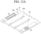
- the first substrate 110 may have one surface contacting an upper heatsink 30 (see FIG. 13 A ) and the other surface bonded to the power elements 100 a and 100 b .
- the second substrate 120 may have one surface contacting a lower heatsink 20 (see FIG. 12 A ) and the other surface bonded to the power elements 100 a and 100 b.
- heat generation may be higher than that of another chip or electric circuit.
- the first substrate 110 and the second substrate 120 which are provided in the sub module 10 , may have excellent thermal conductivity, high electric current mobility, and high electrical insulation properties when compared to another substrate. Also, each of the first substrate 110 and the second substrate 120 may operate sufficiently even at a high temperature.
- each of the first substrate 110 and the second substrate 120 may be implemented as a direct bonded copper (DBC) substrate.
- the first substrate 110 may include a ceramic plate 111 and metal plates 112 , 113 , and 114 disposed on both surfaces of the ceramic plate 111 .
- the second substrate 120 may also include a ceramic plate 121 and metal plates 122 , 123 , 124 , and 125 disposed on both surfaces of the ceramic plate 121 .
- Each of the metal plates 112 to 114 and 122 to 125 may be made of copper (Cu).
- the first substrate 110 and the second substrate 120 of the present disclosure are not only implemented as only DBC substrates, but may also be implemented as various known substrates that are capable of being used in the sub module 10 .
- the first substrate 110 and the second substrate 120 may be provided with the ceramic plates 111 and 121 having the high thermal conductivity between the metal plates 112 to 114 and 122 to 125 to effectively transfer heat generated from the power elements 100 a and 100 b to external heatsinks 20 and 30 .
- Each of the plurality of power elements 100 a and 100 b may include a first power element 100 a in which a gate electrode and an emitter electrode are disposed to face the second substrate 120 and a second power element 100 b in which a gate electrode 102 and an emitter electrode 103 are disposed to face the first substrate 110 .
- Each of the metal plates 112 to 114 and 122 to 125 may have a specific pattern (or shape) to correspond to the electrodes of the power elements to be bonded.
- the metal plates 112 and 113 facing the power elements 100 a and 100 b among the metal plates 112 to 114 of the first substrate 110 may include a metal plate 112 bonded to the gate electrode 102 of the second power element 100 b and a metal plate 113 bonded to the spacer 131 so as to be electrically connected to the collector electrode 104 of the first power element 100 a and simultaneously bonded to the emitter electrode 103 of the second power element 100 b.
- the metal plate 113 may be implemented to be electrically connected to the collector electrode 104 of the first power element 100 a and the emitter electrode 103 of the second power element 100 b .
- the metal plate 113 may be bonded to each of the power elements 100 a and 100 b so as to be separated (a high current pattern is separated from each other).
- the process since the metal plate 113 does not have to be separated, the process may be simplified.
- the metal plate 113 electrically connects the collector electrode 104 of the first power element 100 a to the emitter electrode 103 of the second power element 100 b , a half bridge circuit may be easily implemented without performing the separate process for the electrical connection.
- the metal plates 122 to 124 facing the power elements 100 a and 100 b among the metal plates 122 to 125 of the second substrate 120 may include a metal plate 122 bonded to the gate electrode 102 of the first power element 100 a , a metal plate 123 bonded to the emitter electrode 103 of the first power element 100 a , ad a metal plate 124 bonded to the spacer 131 so as to be electrically connected to the collector electrode 104 of the second power element 100 b.
- each of the metal plates 112 and 122 bonded to the gate electrode 102 may have a pattern to be connected to the terminal. That is, since the gate electrodes 102 of the power elements 100 a and 100 b are connected to the terminals by the metal plates 112 and 122 , a separate wire for connecting the gate electrode to the terminal may not be provided like the related art. Thus, the process of connecting the separate wires may be eliminated to simplify the process and reduce the process time. Also, since the wire is not provided, it is possible to manufacture the more compact sub module 10 and the double-sided cooling type power module.
- Bonding portions 133 to 135 provided by printing a bonding material may be disposed between the metal plates 112 to 113 and 122 to 123 and the power elements 100 a and 100 b or between the metal plates 113 and 124 and the spacer 131 .
- the bonding portions 133 to 135 may be implemented with a material for transferring the heat generated from the power elements 100 a and 100 b to the first substrate 110 and the second substrate 120 .
- the bonding portions 133 to 135 may be implemented with a material such as solder or silver (Ag).
- an insulation portion 140 for insulation may be disposed between the first substrate 110 and the second substrate 120 .
- the insulation portion 140 may be provided by molding an insulation material.
- FIG. 3 is a flowchart showing an example process for manufacturing the double-sided cooling type power module of the present disclosure.
- the process of manufacturing the double-sided cooling type power module may largely include a bonding material printing process, a component bonding process, a terminal forming process, and a heatsink assembly process.
- the bonding material printing process may include operation S 100
- the component bonding process may include operations S 110 to S 130
- the terminal forming process may include operations S 140 to S 150
- the heatsink assembly process may include operation S 160 .
- the bonding material may be printed on each of the first substrate 110 and the second substrate 120 (S 100 ).
- the bonding material may be printed on each of the first substrate 110 and the second substrates 120 . If assuming that the first substrate 110 corresponds to an upper substrate, and the second substrate 120 corresponds to a lower substrate, the bonding material may be applied to each of a bottom surface of the first substrate 110 and a top surface of the second substrate 120 .
- the bonding material may include silver (Ag), solder, or the like, as described above. Since the bonding material is printed, bonding portions 133 to 135 may be formed on each of the first substrate 110 and the second substrate 120 .
- components may be mounted on the second substrate 120 (S 110 ).
- the components may include the plurality of power elements, the plurality of diodes, and a lead frame. Each of the components may be mounted on a bonding position on the second substrate 120 .
- the first power element 100 a may be mounted so that the first electrodes 102 and 103 face the second substrate 120
- the second power element 100 b may be mounted so that the second electrode 104 faces the second substrate 120 .
- sintering of the substrates 110 and 120 and the components may be performed (S 120 ).
- sintering may include heating the substrates 110 and 120 with the bonding material thereon or applying pressure to the substrates 110 and 120 .
- the first substrate 110 and the second substrate 120 may be pressed toward each other, and each of the bonding portions 133 to 135 may be heated to a predetermined temperature.
- the substrates 110 and 120 and the components may be bonded to each other.
- the predetermined temperature may be less than a melting point of the bonding portions 133 . In other examples, the predetermined temperature may be greater than or equal to the melting point of the bonding portions 133 .
- an insulation material may be molded between the first substrate 110 and the second substrate 120 (S 130 ).
- the insulation material may be molded between the first substrate 110 and the second substrate 120 to secure an insulation withstanding voltage of the power element 100 .
- the insulation material since the power element 100 may not be exposed to the outside, the power element 100 may be effectively protected.
- the signal pins and terminals Thereafter, among the lead frame including the signal pins and terminals, remaining portions excluding the signal pins and terminals may be cut, and the signal pins and terminals may be formed in a preset shape (S 140 ).
- the lead frame may include a plurality of signal pins and terminals and a frame to which the signal pins and terminals are fixed. After the lead frame is bonded to the substrates 110 and 120 , since the signal pins and terminals are fixed to the substrates 110 and 120 , the frame may be cut and removed.
- each of the signal pins and terminals may be formed (for example, bent) in a preset shape.
- the insulation material may be molded to insulate the signal pins and terminals (S 150 ). As operation S 150 is performed, the manufacturing of the sub module 10 provided in the double-sided cooling type power module may be completed.
- a plurality of sub modules 10 may be provided in the double-sided cooling type power module 1 (see FIG. 13 B ).
- a heatsink may be assembled on each of both surfaces of each of the plurality of sub modules 10 (S 160 ), and as a result, the double-sided cooling type power module 1 (see FIG. 13 B ) may be manufactured.
- FIGS. 4 to 13 B are views illustrating example stages of the process of manufacturing the double-sided cooling type power module illustrated in FIG. 3 .
- metal plates 122 to 124 and 126 may be formed on the top surface of the second substrate 120 corresponding to the lower substrate.
- the metal plate 122 bonded to the gate electrode 102 of the power element 100 , the metal plate 123 bonded to the emitter electrode 103 , and the metal plate 124 bonded to the spacer 131 so as to be connected to the collector electrode 104 may be formed on the top surface of the second substrate 120 .
- at least one metal plate 126 that is bonded to the signal pin and terminal may be formed on the top surface of the second substrate 120 .
- At least one metal plate 126 may be connected to the metal plates 123 and 124 or may have a shape spaced apart from the metal plates 123 and 124 .
- a portion of the metal plate 122 that is bonded to the gate electrode 102 may be bonded to the gate electrode 102 , and the other portion may be connected to the signal pin or terminal. That is, the metal plate 122 may electrically connect the gate electrode 102 to the signal pin (or terminal). Thus, the gate electrode 102 and the signal pin may be connected without the wire provided in the power module 1 according to the related art.
- Heat may be generated in at least one metal plate 126 that is bonded to the signal pin and terminal as current flows through the signal pin and terminal.
- stress may occur according to a difference in thermal expansion coefficient between the ceramic plate 121 and the metal plate 126 , and the second substrate 120 may be bent or curved due to the stress, and thus, the components may be broken or damaged.
- a plurality of slits 127 may be formed in the metal plate 126 that is bonded to the signal pin and terminal. As illustrated in FIG. 4 , the metal plate 126 may be divided into a plurality of plates, or a plurality of gaps may be formed in the metal plate in a predetermined direction due to the slits 127 .
- each of the gaps may decrease in width due to the slits 127 , and thus, the bending or warpage of the second substrate 120 may be minimized. As a result, the components of the second substrate 120 may be prevented from being broken or damaged.
- a metal plate corresponding to the metal plate 126 may be provided on a bottom surface of the first substrate 110 corresponding to the upper substrate, and a plurality of slits may be formed in the metal plate.
- a bonding material may be printed on the metal plates 122 to 124 and 126 . As the bonding material is printed, bonding portions 133 to 137 may be formed on the second substrate 120 . As described above, the bonding material may include a material such as silver (Ag) or solder.
- the bonding portions 133 to 137 may include the bonding portion 133 bonding the gate electrode 102 of the power element 100 to the metal plate 122 , the bonding portion 134 bonding the emitter electrode 103 to the metal plate 123 , and the bonding portion 135 bonding the collector electrode 104 to the metal plate 124 . Also, the bonding portions 133 to 137 may include a bonding portion 136 bonding the diodes to the metal plates 123 and 124 and a bonding portion 137 bonding the lead frame (the signal pins and terminals) to the metal plate 126 .
- the bonding portions 133 to 137 may bond the power element 100 , the diodes, and the lead frame between the first substrate 110 and the second substrate 120 because a pressure and heat are applied in the sintering process.
- the components (the power elements 100 a and 100 b ), the diodes 150 , and the lead frame 160 may be mounted on the first substrate 110 and the second substrate 120 .
- the first substrate 110 , the components, and the second substrate 120 may be bonded to each other.
- the sub module 10 of the present disclosure is not provided with the wire, it is possible to bond the substrates 110 and 120 to the components through only one sintering process.
- an insulation portion 140 may be formed as the insulation material is molded between the first substrate 110 and the second substrate 120 .
- the insulation portion 140 may include a material such as epoxy molding compound (EMC).
- EMC epoxy molding compound
- the EMC may be a material containing a plurality of raw materials such as silica, an epoxy resin, a phenol resin, carbon black, flame retardant, and the like.
- the insulation withstanding voltage of the power elements 100 a and 100 b may be secured, and the power elements 100 a and 100 b may be effectively protected from external moisture, foreign substances, and shock.
- a frame portion except for the signal pin 161 and terminal 162 in the lead frame 160 may be removed (cut), and the signal pin 161 and terminal 162 may be formed (bent) in a preset shape.
- the insulation material may be molded to secure the insulation of the signal pins 161 and terminals 162 , thereby forming a signal pin and terminal insulation portion 170 .
- the sub module 10 may be manufactured.
- a plurality of sub modules 10 a to 10 c may be coupled between a lower heatsink 20 and an upper heatsink 30 , and thus, the power module 1 may be manufactured.
- the power module 1 includes three sub modules 10 a to 10 c , but the number of sub modules provided in the power module 1 is not limited thereto.
- the lower heatsink 20 may include seating portions 210 a to 210 c on which the sub modules 10 a and 10 c are seated and a plurality of coupling grooves 230 coupled to the upper heatsink 30 .
- the lower heatsink 20 may define a lower portion of the double-sided cooling type power module 1 and shield lower portions of the sub modules 10 a to 10 c from the outside.
- the lower heatsink 20 and the upper heatsink 30 may form a space in which cooling water flows.
- the cooling water may flow into a space of the lower heatsink 20 through a cooling water inflow hole and then flow to a space of the upper heatsink 30 through a first passage 221 formed in the lower heatsink 20 .
- the cooling water flowing into the space in the upper heatsink 30 may flow to the lower heatsink 20 through a second passage 222 , and the cooling water flowing to the lower heatsink 20 may be discharged to the outside through a cooling water discharge hole.
- the heat generated in the sub modules 10 a to 10 c may be conducted to the upper heatsink 30 and the lower heatsink 20 by a heat conduction phenomenon.
- the cooling water flows into the space inside the upper heatsink 30 and the lower heatsink 20 , as the heat conducted to the upper heatsink 30 and the lower heatsink 20 is conducted again to the cooling water, the upper heatsink 30 and the lower heatsink 20 may decrease in temperature.
- the heat of the sub modules 10 a to 10 c may be again conducted to the upper heatsink 30 and the lower heatsink 20 , and thus, the sub modules 10 a to 10 c may decrease in temperature.
- a heat dissipation material may be printed on the seating portions 210 a to 210 c of the lower heatsink 20 .
- the heat dissipation material may include a thermal interface material (TIM) such as thermal grease or a thermally conductive adhesive.
- TIM thermal interface material
- heat dissipation portions 211 a to 211 c may be formed.
- the heat dissipation portions may be formed to also correspond to the upper heatsink 30 .
- the sub modules 10 a to 10 c may be seated (or mounted) on the seating portions 210 a to 210 c.
- the upper heatsink 30 may be assembled.
- the upper heatsink 30 may form an upper portion of the double-sided cooling type power module 1 and shield the upper portions of the sub modules 10 a to 10 c from the outside.
- a coupling groove 310 corresponding to the coupling groove 230 of the lower heatsink 20 may be formed in the upper heatsink 30 .
- a coupling screw 40 may pass through the upper heatsink 30 and then be inserted into and fixed to the coupling groove 230 of the lower heatsink 20 through the coupling groove 310 formed in the upper heatsink 30 . Accordingly, the upper heatsink 30 may be assembled with the lower heatsink 20 .
Abstract
Description
Claims (14)
Applications Claiming Priority (3)
| Application Number | Priority Date | Filing Date | Title |
|---|---|---|---|
| KR1020180032267A KR102048478B1 (en) | 2018-03-20 | 2018-03-20 | Power module of double-faced cooling and method for manufacturing thereof |
| KR10-2018-0032267 | 2018-03-20 | ||
| PCT/KR2018/012402 WO2019182216A1 (en) | 2018-03-20 | 2018-10-19 | Double-sided cooling type power module and manufacturing method therefor |
Related Parent Applications (1)
| Application Number | Title | Priority Date | Filing Date |
|---|---|---|---|
| PCT/KR2018/012402 A-371-Of-International WO2019182216A1 (en) | 2018-03-20 | 2018-10-19 | Double-sided cooling type power module and manufacturing method therefor |
Related Child Applications (1)
| Application Number | Title | Priority Date | Filing Date |
|---|---|---|---|
| US18/375,761 Continuation US20240030177A1 (en) | 2018-03-20 | 2023-10-02 | Double-sided cooling type power module and manufacturing method therefor |
Publications (2)
| Publication Number | Publication Date |
|---|---|
| US20210057372A1 US20210057372A1 (en) | 2021-02-25 |
| US11810887B2 true US11810887B2 (en) | 2023-11-07 |
Family
ID=67987876
Family Applications (2)
| Application Number | Title | Priority Date | Filing Date |
|---|---|---|---|
| US16/982,431 Active 2039-05-27 US11810887B2 (en) | 2018-03-20 | 2018-10-19 | Double-sided cooling type power module and manufacturing method therefor |
| US18/375,761 Pending US20240030177A1 (en) | 2018-03-20 | 2023-10-02 | Double-sided cooling type power module and manufacturing method therefor |
Family Applications After (1)
| Application Number | Title | Priority Date | Filing Date |
|---|---|---|---|
| US18/375,761 Pending US20240030177A1 (en) | 2018-03-20 | 2023-10-02 | Double-sided cooling type power module and manufacturing method therefor |
Country Status (5)
| Country | Link |
|---|---|
| US (2) | US11810887B2 (en) |
| EP (1) | EP3771084A4 (en) |
| JP (1) | JP7204770B2 (en) |
| KR (1) | KR102048478B1 (en) |
| WO (1) | WO2019182216A1 (en) |
Families Citing this family (13)
| Publication number | Priority date | Publication date | Assignee | Title |
|---|---|---|---|---|
| CN115136297A (en) | 2020-02-13 | 2022-09-30 | 阿莫绿色技术有限公司 | Power module and method for manufacturing the same |
| CN115210866A (en) * | 2020-02-19 | 2022-10-18 | 皮尔伯格有限责任公司 | Electric power module |
| WO2021221460A1 (en) * | 2020-04-28 | 2021-11-04 | 주식회사 아모센스 | Adhesive transfer film and method for manufacturing power module substrate by using same |
| KR20210141903A (en) * | 2020-05-15 | 2021-11-23 | 주식회사 아모센스 | Power module |
| WO2021230620A1 (en) * | 2020-05-15 | 2021-11-18 | 주식회사 아모센스 | Power module |
| WO2021230621A1 (en) * | 2020-05-15 | 2021-11-18 | 주식회사 아모센스 | Power module |
| CN111769081B (en) * | 2020-05-28 | 2022-04-29 | 佛山市国星光电股份有限公司 | Integrated module and power device |
| KR102293181B1 (en) * | 2020-08-27 | 2021-08-25 | 주식회사 코멧네트워크 | Ceramic circuit board for power module of double-faced cooling, manufacturing method thereof, power module of double-faced cooling with the same |
| JPWO2022210616A1 (en) * | 2021-03-31 | 2022-10-06 | ||
| KR102588851B1 (en) * | 2021-04-14 | 2023-10-16 | 주식회사 아모센스 | Power module and manufacturing method thereof |
| KR102652471B1 (en) * | 2022-03-07 | 2024-03-29 | 주식회사 세미파워렉스 | The double-sided cooling power module and method thereof |
| KR20240003259A (en) * | 2022-06-30 | 2024-01-08 | 주식회사 아모그린텍 | Power module and manufacturing method thereof |
| WO2024024066A1 (en) * | 2022-07-28 | 2024-02-01 | 日立Astemo株式会社 | Power conversion device |
Citations (44)
| Publication number | Priority date | Publication date | Assignee | Title |
|---|---|---|---|---|
| US6072240A (en) * | 1998-10-16 | 2000-06-06 | Denso Corporation | Semiconductor chip package |
| US6255672B1 (en) * | 1997-11-26 | 2001-07-03 | Kabushiki Kaisha Toshiba | Semiconductor device |
| US20040119148A1 (en) * | 2002-10-04 | 2004-06-24 | Martin Standing | Semiconductor device package |
| JP2006165322A (en) | 2004-12-08 | 2006-06-22 | Denso Corp | Semiconductor module |
| US20060163648A1 (en) * | 2002-05-11 | 2006-07-27 | Henning Hauenstein | Semiconductor component |
| US20070018197A1 (en) * | 2005-07-22 | 2007-01-25 | Denso Corporation | Semiconductor device |
| US20090072384A1 (en) * | 2007-09-14 | 2009-03-19 | Phoenix Precision Technology Corporation | Packaging substrate having heat-dissipating structure |
| US20100078783A1 (en) * | 2008-09-30 | 2010-04-01 | Infineon Technologies Ag | Device including two mounting surfaces |
| CN101847620A (en) | 2009-03-23 | 2010-09-29 | 三菱电机株式会社 | Power module |
| US20100301496A1 (en) * | 2009-05-28 | 2010-12-02 | Texas Instruments Incorporated | Structure and Method for Power Field Effect Transistor |
| US20110062600A1 (en) | 2008-02-14 | 2011-03-17 | Daishi Ueno | Semiconductor element module and method for manufacturing the same |
| US20110108971A1 (en) * | 2009-11-10 | 2011-05-12 | Infineon Technologies Ag | Laminate electronic device |
| JP2012174711A (en) | 2011-02-17 | 2012-09-10 | Denso Corp | Semiconductor device manufacturing method and semiconductor device |
| WO2012132709A1 (en) | 2011-03-29 | 2012-10-04 | ローム株式会社 | Power module semiconductor device |
| US20130003309A1 (en) * | 2011-06-30 | 2013-01-03 | Stmicroelectronics S.R.L. | Half-bridge electronic device with common auxiliary heat sink |
| US20130020694A1 (en) * | 2011-07-19 | 2013-01-24 | Zhenxian Liang | Power module packaging with double sided planar interconnection and heat exchangers |
| JP2013016623A (en) | 2011-07-04 | 2013-01-24 | Denso Corp | Semiconductor device |
| JP2013041939A (en) | 2011-08-12 | 2013-02-28 | Sanyo Electric Co Ltd | Semiconductor module and inverter mounting the same |
| US20130113090A1 (en) * | 2011-11-04 | 2013-05-09 | Takashi Atsumi | Power module, electrical power converter, and electric vehicle |
| US20130146991A1 (en) * | 2011-12-08 | 2013-06-13 | Infineon Technologies Ag | Device Including Two Power Semiconductor Chips and Manufacturing Thereof |
| CN103378048A (en) | 2012-04-12 | 2013-10-30 | 三星电机株式会社 | Semiconductor package, semiconductor module, and mounting structure thereof |
| US20140035112A1 (en) * | 2011-04-19 | 2014-02-06 | Denso Corporation | Semiconductor device and manufacturing method thereof |
| US20140273344A1 (en) * | 2013-03-14 | 2014-09-18 | Vishay-Siliconix | Method for fabricating stack die package |
| US20140264804A1 (en) * | 2013-03-14 | 2014-09-18 | Vishay-Siliconix | Stack die package |
| US8884420B1 (en) * | 2013-07-12 | 2014-11-11 | Infineon Technologies Austria Ag | Multichip device |
| US20150131232A1 (en) * | 2012-06-29 | 2015-05-14 | Denso Corporation | Semiconductor device and semiconductor device connection structure |
| US20150223366A1 (en) * | 2012-09-28 | 2015-08-06 | Hitachi Automotive Systems, Ltd. | Power Conversion Apparatus |
| JP2015225918A (en) | 2014-05-27 | 2015-12-14 | 大学共同利用機関法人 高エネルギー加速器研究機構 | Semiconductor module and semiconductor switch |
| US20150382501A1 (en) * | 2013-02-27 | 2015-12-31 | Hitachi Automotive Systems, Ltd. | Power converter |
| US20160020194A1 (en) * | 2013-03-13 | 2016-01-21 | Schweizer Electronic Ag | Electronic sub-assembly and method for the production of an electronic sub-assembly |
| US20160027711A1 (en) * | 2013-10-03 | 2016-01-28 | Fuji Electric Co., Ltd. | Semiconductor module |
| JP2016039206A (en) | 2014-08-06 | 2016-03-22 | トヨタ自動車株式会社 | Semiconductor device manufacturing method and semiconductor device |
| US9468087B1 (en) | 2015-07-13 | 2016-10-11 | Texas Instruments Incorporated | Power module with improved cooling and method for making |
| US20170018484A1 (en) * | 2014-03-10 | 2017-01-19 | Toyota Jidosha Kabushiki Kaisha | Semiconductor device |
| JP2017034152A (en) | 2015-08-04 | 2017-02-09 | 三菱電機株式会社 | Power semiconductor device |
| US20170077068A1 (en) | 2013-05-16 | 2017-03-16 | Fuji Electric Co., Ltd. | Semiconductor device |
| KR20170069322A (en) | 2015-12-10 | 2017-06-21 | 현대자동차주식회사 | Power module |
| KR20170092750A (en) | 2016-02-03 | 2017-08-14 | 현대자동차주식회사 | Soldering jig for power module of double-faced cooling |
| JP2017163135A (en) | 2016-03-08 | 2017-09-14 | アーベーベー・シュバイツ・アーゲー | Semiconductor module |
| KR20170105284A (en) | 2016-03-09 | 2017-09-19 | 현대자동차주식회사 | Power Module |
| US20170294403A1 (en) * | 2014-02-04 | 2017-10-12 | Infineon Technologies Ag | Chip assembling on adhesion layer or dielectric layer, extending beyond chip, on substrate |
| US20180022220A1 (en) * | 2016-07-20 | 2018-01-25 | Ford Global Technologies, Llc | Signal pin arrangement for multi-device power module |
| US20180337107A1 (en) * | 2017-05-17 | 2018-11-22 | Toyota Jidosha Kabushiki Kaisha | Power converter |
| US20190181078A1 (en) * | 2017-12-08 | 2019-06-13 | Rohm Co., Ltd. | Semiconductor package |
Family Cites Families (1)
| Publication number | Priority date | Publication date | Assignee | Title |
|---|---|---|---|---|
| KR20170068037A (en) * | 2015-12-09 | 2017-06-19 | 현대오트론 주식회사 | Lead frame assembly type power module package |
-
2018
- 2018-03-20 KR KR1020180032267A patent/KR102048478B1/en active IP Right Grant
- 2018-10-19 JP JP2020550787A patent/JP7204770B2/en active Active
- 2018-10-19 US US16/982,431 patent/US11810887B2/en active Active
- 2018-10-19 EP EP18910764.2A patent/EP3771084A4/en active Pending
- 2018-10-19 WO PCT/KR2018/012402 patent/WO2019182216A1/en unknown
-
2023
- 2023-10-02 US US18/375,761 patent/US20240030177A1/en active Pending
Patent Citations (45)
| Publication number | Priority date | Publication date | Assignee | Title |
|---|---|---|---|---|
| US6255672B1 (en) * | 1997-11-26 | 2001-07-03 | Kabushiki Kaisha Toshiba | Semiconductor device |
| US6072240A (en) * | 1998-10-16 | 2000-06-06 | Denso Corporation | Semiconductor chip package |
| US20060163648A1 (en) * | 2002-05-11 | 2006-07-27 | Henning Hauenstein | Semiconductor component |
| US20040119148A1 (en) * | 2002-10-04 | 2004-06-24 | Martin Standing | Semiconductor device package |
| JP2006165322A (en) | 2004-12-08 | 2006-06-22 | Denso Corp | Semiconductor module |
| US20070018197A1 (en) * | 2005-07-22 | 2007-01-25 | Denso Corporation | Semiconductor device |
| US20090072384A1 (en) * | 2007-09-14 | 2009-03-19 | Phoenix Precision Technology Corporation | Packaging substrate having heat-dissipating structure |
| US20110062600A1 (en) | 2008-02-14 | 2011-03-17 | Daishi Ueno | Semiconductor element module and method for manufacturing the same |
| US20100078783A1 (en) * | 2008-09-30 | 2010-04-01 | Infineon Technologies Ag | Device including two mounting surfaces |
| CN101847620A (en) | 2009-03-23 | 2010-09-29 | 三菱电机株式会社 | Power module |
| US20100301496A1 (en) * | 2009-05-28 | 2010-12-02 | Texas Instruments Incorporated | Structure and Method for Power Field Effect Transistor |
| US20110108971A1 (en) * | 2009-11-10 | 2011-05-12 | Infineon Technologies Ag | Laminate electronic device |
| JP2012174711A (en) | 2011-02-17 | 2012-09-10 | Denso Corp | Semiconductor device manufacturing method and semiconductor device |
| WO2012132709A1 (en) | 2011-03-29 | 2012-10-04 | ローム株式会社 | Power module semiconductor device |
| US20140035112A1 (en) * | 2011-04-19 | 2014-02-06 | Denso Corporation | Semiconductor device and manufacturing method thereof |
| US20130003309A1 (en) * | 2011-06-30 | 2013-01-03 | Stmicroelectronics S.R.L. | Half-bridge electronic device with common auxiliary heat sink |
| JP2013016623A (en) | 2011-07-04 | 2013-01-24 | Denso Corp | Semiconductor device |
| US20130020694A1 (en) * | 2011-07-19 | 2013-01-24 | Zhenxian Liang | Power module packaging with double sided planar interconnection and heat exchangers |
| JP2013041939A (en) | 2011-08-12 | 2013-02-28 | Sanyo Electric Co Ltd | Semiconductor module and inverter mounting the same |
| US20130113090A1 (en) * | 2011-11-04 | 2013-05-09 | Takashi Atsumi | Power module, electrical power converter, and electric vehicle |
| US20130146991A1 (en) * | 2011-12-08 | 2013-06-13 | Infineon Technologies Ag | Device Including Two Power Semiconductor Chips and Manufacturing Thereof |
| CN103378048A (en) | 2012-04-12 | 2013-10-30 | 三星电机株式会社 | Semiconductor package, semiconductor module, and mounting structure thereof |
| US20150131232A1 (en) * | 2012-06-29 | 2015-05-14 | Denso Corporation | Semiconductor device and semiconductor device connection structure |
| US20150223366A1 (en) * | 2012-09-28 | 2015-08-06 | Hitachi Automotive Systems, Ltd. | Power Conversion Apparatus |
| US20150382501A1 (en) * | 2013-02-27 | 2015-12-31 | Hitachi Automotive Systems, Ltd. | Power converter |
| US20160020194A1 (en) * | 2013-03-13 | 2016-01-21 | Schweizer Electronic Ag | Electronic sub-assembly and method for the production of an electronic sub-assembly |
| US20140273344A1 (en) * | 2013-03-14 | 2014-09-18 | Vishay-Siliconix | Method for fabricating stack die package |
| US20140264804A1 (en) * | 2013-03-14 | 2014-09-18 | Vishay-Siliconix | Stack die package |
| US20170077068A1 (en) | 2013-05-16 | 2017-03-16 | Fuji Electric Co., Ltd. | Semiconductor device |
| US8884420B1 (en) * | 2013-07-12 | 2014-11-11 | Infineon Technologies Austria Ag | Multichip device |
| US20160027711A1 (en) * | 2013-10-03 | 2016-01-28 | Fuji Electric Co., Ltd. | Semiconductor module |
| US20170294403A1 (en) * | 2014-02-04 | 2017-10-12 | Infineon Technologies Ag | Chip assembling on adhesion layer or dielectric layer, extending beyond chip, on substrate |
| US20170018484A1 (en) * | 2014-03-10 | 2017-01-19 | Toyota Jidosha Kabushiki Kaisha | Semiconductor device |
| JP2015225918A (en) | 2014-05-27 | 2015-12-14 | 大学共同利用機関法人 高エネルギー加速器研究機構 | Semiconductor module and semiconductor switch |
| JP2016039206A (en) | 2014-08-06 | 2016-03-22 | トヨタ自動車株式会社 | Semiconductor device manufacturing method and semiconductor device |
| US9468087B1 (en) | 2015-07-13 | 2016-10-11 | Texas Instruments Incorporated | Power module with improved cooling and method for making |
| JP2017034152A (en) | 2015-08-04 | 2017-02-09 | 三菱電機株式会社 | Power semiconductor device |
| KR20170069322A (en) | 2015-12-10 | 2017-06-21 | 현대자동차주식회사 | Power module |
| KR20170092750A (en) | 2016-02-03 | 2017-08-14 | 현대자동차주식회사 | Soldering jig for power module of double-faced cooling |
| JP2017163135A (en) | 2016-03-08 | 2017-09-14 | アーベーベー・シュバイツ・アーゲー | Semiconductor module |
| US10079193B2 (en) | 2016-03-08 | 2018-09-18 | Abb Schweiz Ag | Semiconductor module |
| KR20170105284A (en) | 2016-03-09 | 2017-09-19 | 현대자동차주식회사 | Power Module |
| US20180022220A1 (en) * | 2016-07-20 | 2018-01-25 | Ford Global Technologies, Llc | Signal pin arrangement for multi-device power module |
| US20180337107A1 (en) * | 2017-05-17 | 2018-11-22 | Toyota Jidosha Kabushiki Kaisha | Power converter |
| US20190181078A1 (en) * | 2017-12-08 | 2019-06-13 | Rohm Co., Ltd. | Semiconductor package |
Non-Patent Citations (4)
| Title |
|---|
| Extended European Search Report in European Appln. No. 18910764.2, dated Nov. 15, 2021, 12 pages. |
| Notice of Allowance in Japanese Appln. No. 2020550787, dated Dec. 6, 2022, 4 pages (with Machine translation). |
| Office Action in Chinese Appln. No. 201880091434.3, dated Apr. 28, 2023, 26 pages (with English translation). |
| Office Action in Japanese Appln. No. 2020-550787, dated Dec. 7, 2021, 7 pages (with English translation). |
Also Published As
| Publication number | Publication date |
|---|---|
| EP3771084A1 (en) | 2021-01-27 |
| EP3771084A4 (en) | 2021-12-15 |
| JP2021516869A (en) | 2021-07-08 |
| US20210057372A1 (en) | 2021-02-25 |
| JP7204770B2 (en) | 2023-01-16 |
| KR20190110376A (en) | 2019-09-30 |
| US20240030177A1 (en) | 2024-01-25 |
| KR102048478B1 (en) | 2019-11-25 |
| WO2019182216A1 (en) | 2019-09-26 |
| CN111903049A (en) | 2020-11-06 |
Similar Documents
| Publication | Publication Date | Title |
|---|---|---|
| US11810887B2 (en) | Double-sided cooling type power module and manufacturing method therefor | |
| US8324726B2 (en) | Semiconductor device, electrode member and electrode member fabrication method | |
| JP4569473B2 (en) | Resin-encapsulated power semiconductor module | |
| CN105531817B (en) | Semiconductor module module unit and semiconductor module | |
| CN107924885B (en) | Structure body | |
| JP5895220B2 (en) | Manufacturing method of semiconductor device | |
| WO2005119896A1 (en) | Inverter device | |
| JP2009536458A (en) | Semiconductor module and manufacturing method thereof | |
| CN104637832A (en) | Semiconductor device and manufacturing method thereof | |
| US20220102249A1 (en) | Dual side cooling power module and manufacturing method of the same | |
| CN109698179B (en) | Semiconductor device and method for manufacturing semiconductor device | |
| JP2012209470A (en) | Semiconductor device, semiconductor device module, and manufacturing method of the semiconductor device | |
| KR20180087330A (en) | Metal slug for double sided cooling of power module | |
| JPH11214612A (en) | Power semiconductor module | |
| JP5619232B2 (en) | Semiconductor device and method for manufacturing electrode member | |
| JP2009206406A (en) | Power semiconductor device | |
| US11735557B2 (en) | Power module of double-faced cooling | |
| CN214848619U (en) | Intelligent power module | |
| JP5195828B2 (en) | Semiconductor device | |
| CN111903049B (en) | Double-sided cooling type power module and manufacturing method thereof | |
| CN115206905A (en) | Semiconductor device and semiconductor module using the same | |
| CN218996706U (en) | Copper strip bonding type power module packaging structure for epoxy plastic package vehicle | |
| US20230282549A1 (en) | Power module for vehicle and method of manufacturing the same | |
| US20240096720A1 (en) | Semiconductor module having a double-sided heat dissipation structure and A Method for fabricating the same | |
| CN115206919A (en) | Semiconductor device with a plurality of semiconductor chips |
Legal Events
| Date | Code | Title | Description |
|---|---|---|---|
| FEPP | Fee payment procedure |
Free format text: ENTITY STATUS SET TO UNDISCOUNTED (ORIGINAL EVENT CODE: BIG.); ENTITY STATUS OF PATENT OWNER: LARGE ENTITY |
|
| AS | Assignment |
Owner name: LG ELECTRONICS INC., KOREA, REPUBLIC OF Free format text: ASSIGNMENT OF ASSIGNORS INTEREST;ASSIGNORS:OH, HEONCHEOL;MIN, JAESANG;PARK, YONGHEE;AND OTHERS;REEL/FRAME:053830/0305 Effective date: 20200904 |
|
| STPP | Information on status: patent application and granting procedure in general |
Free format text: APPLICATION DISPATCHED FROM PREEXAM, NOT YET DOCKETED |
|
| STPP | Information on status: patent application and granting procedure in general |
Free format text: DOCKETED NEW CASE - READY FOR EXAMINATION |
|
| STPP | Information on status: patent application and granting procedure in general |
Free format text: NON FINAL ACTION MAILED |
|
| STPP | Information on status: patent application and granting procedure in general |
Free format text: RESPONSE TO NON-FINAL OFFICE ACTION ENTERED AND FORWARDED TO EXAMINER |
|
| STPP | Information on status: patent application and granting procedure in general |
Free format text: NON FINAL ACTION MAILED |
|
| STPP | Information on status: patent application and granting procedure in general |
Free format text: DOCKETED NEW CASE - READY FOR EXAMINATION |
|
| STPP | Information on status: patent application and granting procedure in general |
Free format text: NOTICE OF ALLOWANCE MAILED -- APPLICATION RECEIVED IN OFFICE OF PUBLICATIONS |
|
| STPP | Information on status: patent application and granting procedure in general |
Free format text: AWAITING TC RESP., ISSUE FEE NOT PAID |
|
| STPP | Information on status: patent application and granting procedure in general |
Free format text: NOTICE OF ALLOWANCE MAILED -- APPLICATION RECEIVED IN OFFICE OF PUBLICATIONS |
|
| STPP | Information on status: patent application and granting procedure in general |
Free format text: PUBLICATIONS -- ISSUE FEE PAYMENT VERIFIED |
|
| STCF | Information on status: patent grant |
Free format text: PATENTED CASE |