WO2012131768A1 - Dispositif à semi-conducteur en carbure de silicium et son procédé de production - Google Patents
Dispositif à semi-conducteur en carbure de silicium et son procédé de production Download PDFInfo
- Publication number
- WO2012131768A1 WO2012131768A1 PCT/JP2011/001886 JP2011001886W WO2012131768A1 WO 2012131768 A1 WO2012131768 A1 WO 2012131768A1 JP 2011001886 W JP2011001886 W JP 2011001886W WO 2012131768 A1 WO2012131768 A1 WO 2012131768A1
- Authority
- WO
- WIPO (PCT)
- Prior art keywords
- silicon carbide
- layer
- semiconductor device
- gate
- region
- Prior art date
Links
- HBMJWWWQQXIZIP-UHFFFAOYSA-N silicon carbide Chemical compound [Si+]#[C-] HBMJWWWQQXIZIP-UHFFFAOYSA-N 0.000 title claims abstract description 86
- 229910010271 silicon carbide Inorganic materials 0.000 title claims abstract description 86
- 239000004065 semiconductor Substances 0.000 title claims description 94
- 238000004519 manufacturing process Methods 0.000 title claims description 39
- 239000000758 substrate Substances 0.000 claims abstract description 46
- 239000012535 impurity Substances 0.000 claims description 26
- 238000005530 etching Methods 0.000 claims description 12
- 238000000034 method Methods 0.000 claims description 12
- PXHVJJICTQNCMI-UHFFFAOYSA-N Nickel Chemical compound [Ni] PXHVJJICTQNCMI-UHFFFAOYSA-N 0.000 claims description 10
- 230000008569 process Effects 0.000 claims description 6
- 229910052751 metal Inorganic materials 0.000 claims description 5
- 239000002184 metal Substances 0.000 claims description 5
- RTAQQCXQSZGOHL-UHFFFAOYSA-N Titanium Chemical compound [Ti] RTAQQCXQSZGOHL-UHFFFAOYSA-N 0.000 claims description 3
- 239000010936 titanium Substances 0.000 claims description 3
- 229910052719 titanium Inorganic materials 0.000 claims description 3
- ZOKXTWBITQBERF-UHFFFAOYSA-N Molybdenum Chemical compound [Mo] ZOKXTWBITQBERF-UHFFFAOYSA-N 0.000 claims description 2
- 229910052750 molybdenum Inorganic materials 0.000 claims description 2
- 239000011733 molybdenum Substances 0.000 claims description 2
- 229910052759 nickel Inorganic materials 0.000 claims description 2
- 150000003377 silicon compounds Chemical class 0.000 claims description 2
- 230000003467 diminishing effect Effects 0.000 abstract 1
- 239000010410 layer Substances 0.000 description 90
- 230000015556 catabolic process Effects 0.000 description 23
- VYPSYNLAJGMNEJ-UHFFFAOYSA-N Silicium dioxide Chemical compound O=[Si]=O VYPSYNLAJGMNEJ-UHFFFAOYSA-N 0.000 description 19
- 229910052814 silicon oxide Inorganic materials 0.000 description 19
- 238000010586 diagram Methods 0.000 description 17
- 238000002513 implantation Methods 0.000 description 15
- KRHYYFGTRYWZRS-UHFFFAOYSA-N Fluorane Chemical compound F KRHYYFGTRYWZRS-UHFFFAOYSA-N 0.000 description 14
- XUIMIQQOPSSXEZ-UHFFFAOYSA-N Silicon Chemical compound [Si] XUIMIQQOPSSXEZ-UHFFFAOYSA-N 0.000 description 13
- 229910052782 aluminium Inorganic materials 0.000 description 13
- XAGFODPZIPBFFR-UHFFFAOYSA-N aluminium Chemical compound [Al] XAGFODPZIPBFFR-UHFFFAOYSA-N 0.000 description 13
- 229910052710 silicon Inorganic materials 0.000 description 13
- 239000010703 silicon Substances 0.000 description 13
- 150000002500 ions Chemical class 0.000 description 12
- 239000000463 material Substances 0.000 description 12
- IJGRMHOSHXDMSA-UHFFFAOYSA-N Atomic nitrogen Chemical compound N#N IJGRMHOSHXDMSA-UHFFFAOYSA-N 0.000 description 10
- 239000011229 interlayer Substances 0.000 description 10
- 238000001312 dry etching Methods 0.000 description 9
- 238000005468 ion implantation Methods 0.000 description 9
- 238000000137 annealing Methods 0.000 description 7
- 241000894007 species Species 0.000 description 7
- 238000001459 lithography Methods 0.000 description 6
- 229910052757 nitrogen Inorganic materials 0.000 description 5
- 229910021417 amorphous silicon Inorganic materials 0.000 description 4
- 238000009792 diffusion process Methods 0.000 description 4
- 230000005684 electric field Effects 0.000 description 4
- 230000003647 oxidation Effects 0.000 description 4
- 238000007254 oxidation reaction Methods 0.000 description 4
- 229910021332 silicide Inorganic materials 0.000 description 4
- FVBUAEGBCNSCDD-UHFFFAOYSA-N silicide(4-) Chemical compound [Si-4] FVBUAEGBCNSCDD-UHFFFAOYSA-N 0.000 description 4
- 230000004913 activation Effects 0.000 description 3
- QVGXLLKOCUKJST-UHFFFAOYSA-N atomic oxygen Chemical compound [O] QVGXLLKOCUKJST-UHFFFAOYSA-N 0.000 description 3
- 230000004888 barrier function Effects 0.000 description 3
- 230000015572 biosynthetic process Effects 0.000 description 3
- 230000000903 blocking effect Effects 0.000 description 3
- 230000008859 change Effects 0.000 description 3
- 230000000694 effects Effects 0.000 description 3
- 239000001301 oxygen Substances 0.000 description 3
- 229910052760 oxygen Inorganic materials 0.000 description 3
- 230000009467 reduction Effects 0.000 description 3
- XKRFYHLGVUSROY-UHFFFAOYSA-N Argon Chemical compound [Ar] XKRFYHLGVUSROY-UHFFFAOYSA-N 0.000 description 2
- OKTJSMMVPCPJKN-UHFFFAOYSA-N Carbon Chemical compound [C] OKTJSMMVPCPJKN-UHFFFAOYSA-N 0.000 description 2
- 235000004522 Pentaglottis sempervirens Nutrition 0.000 description 2
- 238000010306 acid treatment Methods 0.000 description 2
- 229910045601 alloy Inorganic materials 0.000 description 2
- 239000000956 alloy Substances 0.000 description 2
- 239000012298 atmosphere Substances 0.000 description 2
- 229910052799 carbon Inorganic materials 0.000 description 2
- 230000006872 improvement Effects 0.000 description 2
- 238000002955 isolation Methods 0.000 description 2
- 230000003071 parasitic effect Effects 0.000 description 2
- 230000002093 peripheral effect Effects 0.000 description 2
- 238000001039 wet etching Methods 0.000 description 2
- ZOXJGFHDIHLPTG-UHFFFAOYSA-N Boron Chemical compound [B] ZOXJGFHDIHLPTG-UHFFFAOYSA-N 0.000 description 1
- 229910002601 GaN Inorganic materials 0.000 description 1
- JMASRVWKEDWRBT-UHFFFAOYSA-N Gallium nitride Chemical compound [Ga]#N JMASRVWKEDWRBT-UHFFFAOYSA-N 0.000 description 1
- 240000004050 Pentaglottis sempervirens Species 0.000 description 1
- OAICVXFJPJFONN-UHFFFAOYSA-N Phosphorus Chemical compound [P] OAICVXFJPJFONN-UHFFFAOYSA-N 0.000 description 1
- NRTOMJZYCJJWKI-UHFFFAOYSA-N Titanium nitride Chemical compound [Ti]#N NRTOMJZYCJJWKI-UHFFFAOYSA-N 0.000 description 1
- 229910052786 argon Inorganic materials 0.000 description 1
- 239000012300 argon atmosphere Substances 0.000 description 1
- 238000004380 ashing Methods 0.000 description 1
- 230000008901 benefit Effects 0.000 description 1
- 229910052796 boron Inorganic materials 0.000 description 1
- 239000000969 carrier Substances 0.000 description 1
- 239000012141 concentrate Substances 0.000 description 1
- PMHQVHHXPFUNSP-UHFFFAOYSA-M copper(1+);methylsulfanylmethane;bromide Chemical compound Br[Cu].CSC PMHQVHHXPFUNSP-UHFFFAOYSA-M 0.000 description 1
- 230000007423 decrease Effects 0.000 description 1
- 230000006866 deterioration Effects 0.000 description 1
- KPUWHANPEXNPJT-UHFFFAOYSA-N disiloxane Chemical class [SiH3]O[SiH3] KPUWHANPEXNPJT-UHFFFAOYSA-N 0.000 description 1
- 238000005516 engineering process Methods 0.000 description 1
- 230000005669 field effect Effects 0.000 description 1
- 230000002209 hydrophobic effect Effects 0.000 description 1
- 238000009413 insulation Methods 0.000 description 1
- 230000007257 malfunction Effects 0.000 description 1
- 229910044991 metal oxide Inorganic materials 0.000 description 1
- 150000004706 metal oxides Chemical class 0.000 description 1
- 229910003465 moissanite Inorganic materials 0.000 description 1
- 229910052698 phosphorus Inorganic materials 0.000 description 1
- 239000011574 phosphorus Substances 0.000 description 1
- 229910021420 polycrystalline silicon Inorganic materials 0.000 description 1
- 229920005591 polysilicon Polymers 0.000 description 1
- 239000002243 precursor Substances 0.000 description 1
- 238000005476 soldering Methods 0.000 description 1
- 238000004544 sputter deposition Methods 0.000 description 1
Images


Classifications
-
- H—ELECTRICITY
- H01—ELECTRIC ELEMENTS
- H01L—SEMICONDUCTOR DEVICES NOT COVERED BY CLASS H10
- H01L21/00—Processes or apparatus adapted for the manufacture or treatment of semiconductor or solid state devices or of parts thereof
- H01L21/70—Manufacture or treatment of devices consisting of a plurality of solid state components formed in or on a common substrate or of parts thereof; Manufacture of integrated circuit devices or of parts thereof
- H01L21/77—Manufacture or treatment of devices consisting of a plurality of solid state components or integrated circuits formed in, or on, a common substrate
- H01L21/78—Manufacture or treatment of devices consisting of a plurality of solid state components or integrated circuits formed in, or on, a common substrate with subsequent division of the substrate into plural individual devices
- H01L21/82—Manufacture or treatment of devices consisting of a plurality of solid state components or integrated circuits formed in, or on, a common substrate with subsequent division of the substrate into plural individual devices to produce devices, e.g. integrated circuits, each consisting of a plurality of components
- H01L21/8213—Manufacture or treatment of devices consisting of a plurality of solid state components or integrated circuits formed in, or on, a common substrate with subsequent division of the substrate into plural individual devices to produce devices, e.g. integrated circuits, each consisting of a plurality of components the substrate being a semiconductor, using SiC technology
-
- H—ELECTRICITY
- H01—ELECTRIC ELEMENTS
- H01L—SEMICONDUCTOR DEVICES NOT COVERED BY CLASS H10
- H01L29/00—Semiconductor devices adapted for rectifying, amplifying, oscillating or switching, or capacitors or resistors with at least one potential-jump barrier or surface barrier, e.g. PN junction depletion layer or carrier concentration layer; Details of semiconductor bodies or of electrodes thereof ; Multistep manufacturing processes therefor
- H01L29/02—Semiconductor bodies ; Multistep manufacturing processes therefor
- H01L29/06—Semiconductor bodies ; Multistep manufacturing processes therefor characterised by their shape; characterised by the shapes, relative sizes, or dispositions of the semiconductor regions ; characterised by the concentration or distribution of impurities within semiconductor regions
- H01L29/0603—Semiconductor bodies ; Multistep manufacturing processes therefor characterised by their shape; characterised by the shapes, relative sizes, or dispositions of the semiconductor regions ; characterised by the concentration or distribution of impurities within semiconductor regions characterised by particular constructional design considerations, e.g. for preventing surface leakage, for controlling electric field concentration or for internal isolations regions
- H01L29/0607—Semiconductor bodies ; Multistep manufacturing processes therefor characterised by their shape; characterised by the shapes, relative sizes, or dispositions of the semiconductor regions ; characterised by the concentration or distribution of impurities within semiconductor regions characterised by particular constructional design considerations, e.g. for preventing surface leakage, for controlling electric field concentration or for internal isolations regions for preventing surface leakage or controlling electric field concentration
- H01L29/0611—Semiconductor bodies ; Multistep manufacturing processes therefor characterised by their shape; characterised by the shapes, relative sizes, or dispositions of the semiconductor regions ; characterised by the concentration or distribution of impurities within semiconductor regions characterised by particular constructional design considerations, e.g. for preventing surface leakage, for controlling electric field concentration or for internal isolations regions for preventing surface leakage or controlling electric field concentration for increasing or controlling the breakdown voltage of reverse biased devices
- H01L29/0615—Semiconductor bodies ; Multistep manufacturing processes therefor characterised by their shape; characterised by the shapes, relative sizes, or dispositions of the semiconductor regions ; characterised by the concentration or distribution of impurities within semiconductor regions characterised by particular constructional design considerations, e.g. for preventing surface leakage, for controlling electric field concentration or for internal isolations regions for preventing surface leakage or controlling electric field concentration for increasing or controlling the breakdown voltage of reverse biased devices by the doping profile or the shape or the arrangement of the PN junction, or with supplementary regions, e.g. junction termination extension [JTE]
- H01L29/0619—Semiconductor bodies ; Multistep manufacturing processes therefor characterised by their shape; characterised by the shapes, relative sizes, or dispositions of the semiconductor regions ; characterised by the concentration or distribution of impurities within semiconductor regions characterised by particular constructional design considerations, e.g. for preventing surface leakage, for controlling electric field concentration or for internal isolations regions for preventing surface leakage or controlling electric field concentration for increasing or controlling the breakdown voltage of reverse biased devices by the doping profile or the shape or the arrangement of the PN junction, or with supplementary regions, e.g. junction termination extension [JTE] with a supplementary region doped oppositely to or in rectifying contact with the semiconductor containing or contacting region, e.g. guard rings with PN or Schottky junction
-
- H—ELECTRICITY
- H01—ELECTRIC ELEMENTS
- H01L—SEMICONDUCTOR DEVICES NOT COVERED BY CLASS H10
- H01L29/00—Semiconductor devices adapted for rectifying, amplifying, oscillating or switching, or capacitors or resistors with at least one potential-jump barrier or surface barrier, e.g. PN junction depletion layer or carrier concentration layer; Details of semiconductor bodies or of electrodes thereof ; Multistep manufacturing processes therefor
- H01L29/02—Semiconductor bodies ; Multistep manufacturing processes therefor
- H01L29/06—Semiconductor bodies ; Multistep manufacturing processes therefor characterised by their shape; characterised by the shapes, relative sizes, or dispositions of the semiconductor regions ; characterised by the concentration or distribution of impurities within semiconductor regions
- H01L29/10—Semiconductor bodies ; Multistep manufacturing processes therefor characterised by their shape; characterised by the shapes, relative sizes, or dispositions of the semiconductor regions ; characterised by the concentration or distribution of impurities within semiconductor regions with semiconductor regions connected to an electrode not carrying current to be rectified, amplified or switched and such electrode being part of a semiconductor device which comprises three or more electrodes
- H01L29/1066—Gate region of field-effect devices with PN junction gate
-
- H—ELECTRICITY
- H01—ELECTRIC ELEMENTS
- H01L—SEMICONDUCTOR DEVICES NOT COVERED BY CLASS H10
- H01L29/00—Semiconductor devices adapted for rectifying, amplifying, oscillating or switching, or capacitors or resistors with at least one potential-jump barrier or surface barrier, e.g. PN junction depletion layer or carrier concentration layer; Details of semiconductor bodies or of electrodes thereof ; Multistep manufacturing processes therefor
- H01L29/66—Types of semiconductor device ; Multistep manufacturing processes therefor
- H01L29/66007—Multistep manufacturing processes
- H01L29/66053—Multistep manufacturing processes of devices having a semiconductor body comprising crystalline silicon carbide
- H01L29/66068—Multistep manufacturing processes of devices having a semiconductor body comprising crystalline silicon carbide the devices being controllable only by the electric current supplied or the electric potential applied, to an electrode which does not carry the current to be rectified, amplified or switched, e.g. three-terminal devices
-
- H—ELECTRICITY
- H01—ELECTRIC ELEMENTS
- H01L—SEMICONDUCTOR DEVICES NOT COVERED BY CLASS H10
- H01L29/00—Semiconductor devices adapted for rectifying, amplifying, oscillating or switching, or capacitors or resistors with at least one potential-jump barrier or surface barrier, e.g. PN junction depletion layer or carrier concentration layer; Details of semiconductor bodies or of electrodes thereof ; Multistep manufacturing processes therefor
- H01L29/66—Types of semiconductor device ; Multistep manufacturing processes therefor
- H01L29/68—Types of semiconductor device ; Multistep manufacturing processes therefor controllable by only the electric current supplied, or only the electric potential applied, to an electrode which does not carry the current to be rectified, amplified or switched
- H01L29/76—Unipolar devices, e.g. field effect transistors
- H01L29/772—Field effect transistors
- H01L29/80—Field effect transistors with field effect produced by a PN or other rectifying junction gate, i.e. potential-jump barrier
- H01L29/808—Field effect transistors with field effect produced by a PN or other rectifying junction gate, i.e. potential-jump barrier with a PN junction gate, e.g. PN homojunction gate
- H01L29/8083—Vertical transistors
-
- H—ELECTRICITY
- H01—ELECTRIC ELEMENTS
- H01L—SEMICONDUCTOR DEVICES NOT COVERED BY CLASS H10
- H01L2224/00—Indexing scheme for arrangements for connecting or disconnecting semiconductor or solid-state bodies and methods related thereto as covered by H01L24/00
- H01L2224/01—Means for bonding being attached to, or being formed on, the surface to be connected, e.g. chip-to-package, die-attach, "first-level" interconnects; Manufacturing methods related thereto
- H01L2224/02—Bonding areas; Manufacturing methods related thereto
- H01L2224/04—Structure, shape, material or disposition of the bonding areas prior to the connecting process
- H01L2224/06—Structure, shape, material or disposition of the bonding areas prior to the connecting process of a plurality of bonding areas
- H01L2224/0601—Structure
- H01L2224/0603—Bonding areas having different sizes, e.g. different heights or widths
-
- H—ELECTRICITY
- H01—ELECTRIC ELEMENTS
- H01L—SEMICONDUCTOR DEVICES NOT COVERED BY CLASS H10
- H01L2224/00—Indexing scheme for arrangements for connecting or disconnecting semiconductor or solid-state bodies and methods related thereto as covered by H01L24/00
- H01L2224/01—Means for bonding being attached to, or being formed on, the surface to be connected, e.g. chip-to-package, die-attach, "first-level" interconnects; Manufacturing methods related thereto
- H01L2224/42—Wire connectors; Manufacturing methods related thereto
- H01L2224/47—Structure, shape, material or disposition of the wire connectors after the connecting process
- H01L2224/48—Structure, shape, material or disposition of the wire connectors after the connecting process of an individual wire connector
- H01L2224/4805—Shape
- H01L2224/4809—Loop shape
- H01L2224/48091—Arched
-
- H—ELECTRICITY
- H01—ELECTRIC ELEMENTS
- H01L—SEMICONDUCTOR DEVICES NOT COVERED BY CLASS H10
- H01L29/00—Semiconductor devices adapted for rectifying, amplifying, oscillating or switching, or capacitors or resistors with at least one potential-jump barrier or surface barrier, e.g. PN junction depletion layer or carrier concentration layer; Details of semiconductor bodies or of electrodes thereof ; Multistep manufacturing processes therefor
- H01L29/02—Semiconductor bodies ; Multistep manufacturing processes therefor
- H01L29/12—Semiconductor bodies ; Multistep manufacturing processes therefor characterised by the materials of which they are formed
- H01L29/16—Semiconductor bodies ; Multistep manufacturing processes therefor characterised by the materials of which they are formed including, apart from doping materials or other impurities, only elements of Group IV of the Periodic System
- H01L29/1608—Silicon carbide
-
- H—ELECTRICITY
- H01—ELECTRIC ELEMENTS
- H01L—SEMICONDUCTOR DEVICES NOT COVERED BY CLASS H10
- H01L2924/00—Indexing scheme for arrangements or methods for connecting or disconnecting semiconductor or solid-state bodies as covered by H01L24/00
- H01L2924/10—Details of semiconductor or other solid state devices to be connected
- H01L2924/11—Device type
- H01L2924/13—Discrete devices, e.g. 3 terminal devices
- H01L2924/1304—Transistor
- H01L2924/1305—Bipolar Junction Transistor [BJT]
- H01L2924/13055—Insulated gate bipolar transistor [IGBT]
-
- H—ELECTRICITY
- H01—ELECTRIC ELEMENTS
- H01L—SEMICONDUCTOR DEVICES NOT COVERED BY CLASS H10
- H01L2924/00—Indexing scheme for arrangements or methods for connecting or disconnecting semiconductor or solid-state bodies as covered by H01L24/00
- H01L2924/10—Details of semiconductor or other solid state devices to be connected
- H01L2924/11—Device type
- H01L2924/13—Discrete devices, e.g. 3 terminal devices
- H01L2924/1304—Transistor
- H01L2924/1306—Field-effect transistor [FET]
- H01L2924/13091—Metal-Oxide-Semiconductor Field-Effect Transistor [MOSFET]
Definitions
- the breakdown voltage strength depends on the band gap size of the substrate material, it is easy to secure a breakdown voltage by using a material having a large band gap as the substrate material. That is, when using a material having a large band gap than silicon as the substrate material, as in the case of silicon, n - and increasing the thickness of the drift region, and, n - impurity concentration of the drift region not lower Can withstand pressure. That is, by using a material having a larger band gap than that of silicon as a substrate material, the n ⁇ drift region can be made thinner and thinner than in the case of silicon in order to ensure a breakdown voltage equivalent to that of silicon. - results it is possible to increase the impurity concentration of the drift region, it is possible to reduce the on-resistance between the n + source regions and n + drain region.
- normally-on type junction FETs normally have a channel turned on and current flows, and when the channel needs to be turned off, a negative voltage is applied to the gate to extend the depletion layer from the pn junction and Turn off. Therefore, when the gate of the junction FET is broken for some reason, the current continues to flow with the channel turned on. Normally, it is desirable from the viewpoint of safety that the current does not flow when the junction FET is broken. However, in the normally-on type junction FET, the current continues to flow even when the gate of the junction FET is broken, so the application is limited. It is.
- a normally-off type is generally desired for a semiconductor power device.
- the silicon junction FET it becomes difficult for the silicon junction FET to be normally off and have a high breakdown voltage. This is because, since the diffusion potential of the silicon pn junction is small, the depletion layer cannot be sufficiently extended from the pn junction without applying a voltage to the gate layer, and the channel cannot be completely turned off. It is. That is, in the silicon junction FET, it is necessary to apply a negative voltage to the gate layer in order to turn off the channel, and it becomes difficult to realize a normally-off state. On the other hand, in a junction FET using silicon carbide, a high breakdown voltage can be realized with a normally-off junction FET by narrowing the channel width.
- the charge / discharge current is proportional to the capacity and the rate of change of voltage per time, if the capacity between the gate and drain is large, a large current instantaneously flows through the gate during switching. A large instantaneous current flowing through the gate may destroy the gate driver. Conversely, in order not to destroy the gate driver, it is necessary to develop a gate driver that can flow even a large current, resulting in a very high cost. From the above viewpoint, it is necessary to keep the capacitance between the gate and drain small. However, the capacitance between the gate and drain of the trench-type normally-off junction FET is determined by the p region of the gate and the pn junction of the drift layer. To simply reduce the capacitance, the concentration of the drift layer must be lowered. However, since the on-resistance increases when the concentration of the drift layer is lowered, it can be said that there is a trade-off between reducing the gate-drain capacitance and reducing the on-resistance.
- a structure that can reduce the gate-drain capacitance without increasing the on-resistance, a structure has been proposed in which a p region is formed at the bottom of the trench separately from the gate, and the p region is short-circuited to the source.
- the area of the gate region forming the pn junction with the drift layer is about half that of the conventional one, so that the gate-drain capacitance can be reduced to about half of the conventional one.
- half of the capacitance between the gate and drain is not sufficient, and further reduction is necessary.
- it is necessary to provide a certain distance between the gate and the source in order to ensure the breakdown voltage between the gate and the source.
- the capacitance between the gate and the drain could not be reduced without lowering the breakdown voltage and on-resistance performance.
- the capacitance between the gate and drain cannot be reduced without increasing the trench bottom area (trench width).
- the gate is only the upper part of the sidewall of the trench, and the p region formed at the bottom of the trench and short-circuited with the source is perpendicular to the substrate surface.
- the present invention relates to a drain layer of a first conductivity type provided on a silicon carbide substrate, a silicon carbide layer of a first conductivity type formed on the drain layer, a plurality of trenches formed in the silicon carbide layer, and a trench
- a first conductivity type source layer formed on the surface of the silicon carbide layer in the region and a second conductivity type opposite to the first conductivity type formed on the side surface of the trench.
- a third electrode connected to the gate layer, the drift layer side end of the gate layer being formed closer to the surface side of the silicon carbide substrate than the bottom surface of the trench Device.
- a method for manufacturing a silicon carbide semiconductor device comprising a.
- Another invention of the present application is a silicon carbide substrate including a first conductivity type silicon carbide layer formed on a first conductivity type drain layer, wherein an impurity of the silicon carbide layer is formed on the surface of the silicon carbide layer.
- the bottom of the p region (p semiconductor layer) formed at the bottom of the trench and short-circuited with the source is sufficiently deep with respect to the bottom of the gate p region, and the gate region is shielded by the depletion layer extending from the trench bottom p region. This reduces the capacitance between the gate and drain.
- the gate region and the trench bottom p region are spaced from each other in the direction perpendicular to the substrate surface, the breakdown voltage between the gate and the source can be ensured without increasing the trench width (cell pitch).
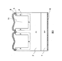
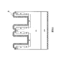
- FIG. 1 is a cross-sectional structure diagram of a first embodiment of a semiconductor device according to the present invention
- 1 is a schematic cross-sectional structure diagram of Patent Document 1.
- FIG. It is a figure which shows the manufacturing method of the 1st Example of the semiconductor device by this invention. It is a figure which shows the manufacturing method of the 1st Example of the semiconductor device by this invention. It is a figure which shows the manufacturing method of the 1st Example of the semiconductor device by this invention. It is a figure which shows the manufacturing method of the 1st Example of the semiconductor device by this invention. It is a figure which shows the manufacturing method of the 1st Example of the semiconductor device by this invention. It is a figure which shows the manufacturing method of the 1st Example of the semiconductor device by this invention. It is a figure which shows the manufacturing method of the 1st Example of the semiconductor device by this invention. It is a figure which shows the manufacturing method of the 1st Example of the semiconductor device by this invention.
- FIG. 1 is a chip image of a first embodiment of a semiconductor device according to the present invention. It is an example of the plane layout of the 1st Example of the semiconductor device by this invention.
- FIG. 6 is a characteristic diagram of the first embodiment of the semiconductor device according to the present invention. It is explanatory drawing of the characteristic of the 1st Example of the semiconductor device by this invention.
- FIG. 6 is a characteristic diagram of the first embodiment of the semiconductor device according to the present invention.
- FIG. 1 It is a figure which shows the manufacturing method of the 2nd Example of the semiconductor device by this invention. It is a figure which shows the manufacturing method of the 2nd Example of the semiconductor device by this invention. It is a figure which shows the manufacturing method of the 2nd Example of the semiconductor device by this invention. It is a figure which shows the manufacturing method of the 2nd Example of the semiconductor device by this invention. It is a figure which shows the manufacturing method of the 2nd Example of the semiconductor device by this invention. It is a figure which shows the manufacturing method of the 2nd Example of the semiconductor device by this invention. It is a figure which shows the manufacturing method of the 2nd Example of the semiconductor device by this invention. It is a figure which shows the manufacturing method of the 2nd Example of the semiconductor device by this invention. It is a figure which shows the manufacturing method of the 2nd Example of the semiconductor device by this invention. FIG.
- FIG. 6 is an equivalent circuit diagram of a second embodiment of the semiconductor device according to the present invention. It is a bird's-eye view of the 3rd example at the time of mounting a semiconductor device by the present invention. It is a circuit diagram of the gate driver of the 4th Example of the semiconductor device by this invention. It is a circuit diagram of the 5th example at the time of applying a semiconductor device by the present invention to an inverter. It is an equivalent circuit diagram of junction FET.
- FIG. 1 shows a cross-sectional structure diagram of the junction FET of Example 1 of the present invention
- FIG. 2 shows a schematic cross-sectional structure diagram of the junction FET of Patent Document 1 for comparison.
- An n ⁇ drift layer (silicon carbide layer) 2 is formed by epitaxial growth on an n + substrate (silicon carbide substrate) 1 serving as a drain region, and p is formed on the drift layer 2 on the surface of the n + source region 3 and the trench 11.
- a gate region 4 is formed. That is, the end of the p gate region 4 on the drift layer side is formed on the substrate surface side with respect to the bottom surface of the trench 11.
- a p region 6 is formed at the bottom of the trench 11, and the p region 6 is electrically separated from the gate region 4 by an n region 5 formed below the trench side wall.
- the n region 5 is not necessarily essential.
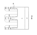
- the figure shows only the active region through which current flows, but a termination region for electric field relaxation is formed around the active region.
- the drain contact region 10 is formed on the back side, and the source contact region 8 and the trench bottom contact region 7 are formed on the front side by ohmic contact. Source contact region 8 and trench bottom contact region 7 are electrically connected by source electrode 9.
- the front side is provided with a two-layer aluminum wiring, and has a three-terminal structure of a front source pad, a gate pad and a back drain pad.
- the side wall and bottom of the trench 11 are all covered with the p region 4 and connected to the gate electrode.
- the structure around the trench 11 is greatly different in structure.
- FIG. 16 is an equivalent circuit diagram showing the parasitic capacitance existing in the junction FET.
- the junction FET has parasitic capacitances (Cgs, Cgd, Csd) between the terminals of the gate (G), the source (S), and the drain (D), greatly affecting the device characteristics.
- the capacitance (Cgd) between the gate and the drain which is important for switching is determined by the capacitance of the pn junction between the trench bottom p region 6 and the drift layer 2 in the structure of FIG.
- a voltage of 100 V to several kV is applied to the drain with 0 V or a negative voltage applied to the gate.
- the channel has the entire depletion layer extending from the gate, and an energy barrier is created between the source and the channel. Thereby, a blocking state can be maintained.
- a voltage of about 2.5 V is applied to the gate and a voltage of about 1-2 V is applied to the drain.
- the depletion layer between the gate and the channel is narrowed to create a carrier path, so that carriers flow from the source by the voltage applied to the drain.
- the gate voltage is switched from on to off or from off to on.
- the voltage applied to the drain rapidly changes from several hundred volts to about 1 volts. Due to the change in the drain voltage, charge and discharge occur in the gate-drain capacitance and the source-drain capacitance, and current flows. At this time, the charge / discharge current is proportional to the drain voltage change rate and each capacitance. Therefore, a current corresponding to each capacitance flows through the source and gate.
- the gate-drain capacitance is significantly reduced as compared with FIG. 2, the current flowing through the gate is kept low.
- the concentration of the drift layer is 2 ⁇ 10 16 cm ⁇ 3
- the thickness is 7 ⁇ m
- the depth of the trench is 1.8 ⁇ m
- the width is 1 ⁇ m. Since the width of the source is directly related to device characteristics, particularly the threshold voltage, the width is set to about 0.8 to 1.0 ⁇ m.
- the gate and trench bottom p regions are p-type with aluminum as an impurity, and peak concentrations are about 10 18 and 10 19 cm ⁇ 3 , respectively.
- the n region under the trench sidewall separating the gate region and the trench bottom p region has nitrogen as an impurity
- the impurity concentration is about 10 17 cm ⁇ 3
- the distance between the gate region and the trench bottom p region is about 0.8 ⁇ m.
- This impurity concentration is higher than that of n ⁇ drift layer (silicon carbide layer) 2. If the distance is less than 0.5 ⁇ m, punch-through occurs when a voltage is applied to the gate, and current flows between the gate and the source. In the first embodiment, it is about 0.8 ⁇ m with a margin.
- the ion species is aluminum and the concentration is about 1 ⁇ 10 17 cm ⁇ 3 . Since the termination region needs to be deeper than the gate region, a multi-stage implantation of 2 MeV at the maximum is necessary. In this embodiment, a JTE (Junction Termination Extension) structure is adopted, but a guard ring structure, a mesa structure, or other structures may be used.
- a JTE (Junction Termination Extension) structure is adopted, but a guard ring structure, a mesa structure, or other structures may be used.
- an n + region 3 serving as a source and a p + region serving as a gate contact region are formed by the same method as the termination region forming method. In the drawing, an n + region is formed on the entire surface, but a gate contact region and a termination region are not shown because a cross section of a main part of the device is shown.
- n + is nitrogen
- p + is aluminum
- n + ion implantation is performed at 500 ° C.
- silicon oxide is deposited as a trench processing hard mask
- silicon oxide 21 is processed by lithography and dry etching
- trenches are formed by dry etching using the silicon oxide 21 as a hard mask.
- the trench should be as vertical as possible.
- the trench depth is about 1.0 ⁇ m.
- a p region (semiconductor layer) 22 to be a gate is formed on the side surface of the trench by ion implantation using a trench processing hard mask as it is.
- the trench is further etched and dug using the hard mask in the previous process.
- the depth of digging at this time is about 0.8 ⁇ m, and all the p region at the bottom of the trench implanted in all steps is removed.
- this depth is desirably 0.5 ⁇ m or more in order to avoid the above-described punch-through.
- a p region 6 is formed on the entire bottom of the trench.
- the ion species was aluminum, and implantation was performed at a maximum of 100 keV in the vertical direction. At this time, even in the vertical implantation, ions are implanted also into the lower portion of the trench side wall due to the rebound of ions, and the p region is formed. In order to strike back this region, an n-type impurity is obliquely implanted as shown in FIG.
- the ion species was nitrogen and the energy was 50 eV.
- the concentration of the n region 23 returned is too high, the electric field tends to concentrate and the breakdown voltage is lowered. Therefore, the concentration is set to about 10 17 cm ⁇ 3 so that the breakdown voltage is not lowered.
- this oblique implantation has an effect of ensuring electrical isolation between the p region 22 and the p region 6, it is desirable to perform the oblique implantation.
- the impurity concentration is too high, there is a problem that the withstand voltage is lowered. Therefore, it is not necessary to make it higher than necessary, but it is desirable to make it higher than the impurity concentration of the drift layer.
- activation annealing is performed in an argon atmosphere at about 1650 ° C., and an interlayer insulating film 24 is formed after sacrificial oxidation (FIG. 3G).
- an alloy containing Ni as a main component is formed on the front and back of the silicon carbide substrate.
- contact holes are formed by lithography and dry etching, Ni is deposited, silicide is formed by silicidation annealing at 1000 degrees, and unreacted metal is finally removed. Thereby, trench bottom contact region 7 and source contact region 8 are formed. Similarly, Ni is deposited on the back side, and silicide is formed by silicidation annealing at 1000 degrees.
- the drain contact region 10 is formed. Thereafter, as shown in FIG. 3I, the source contact and the contact at the bottom of the trench are connected by the aluminum wiring 9. Finally, an aluminum two-layer wiring using silicon oxide as an interlayer insulating film is formed, and a source pad connected to the aluminum wiring 9 and a gate pad connected to the gate region 4 are opened to complete the device.
- the impurity in the p region is aluminum and the impurity in the n region is nitrogen.
- the p region may be boron and the n-type region may be phosphorus.
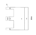
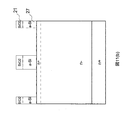
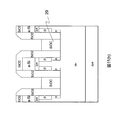
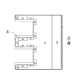
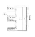
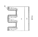
- FIG. 4 shows a chip layout of this embodiment. There is an active region surrounded by the termination region, and a source pad 25 is disposed on the active region. A gate pad 26 is disposed beside the source pad 25.
- the chip size is active and is 2.0 mm 2 .
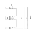
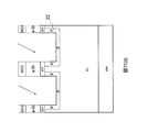
- Figure 5 shows the layout of the active area.
- Trench 11 is formed in a line shape so as to be surrounded by n + source region 3 and p + gate lead region 9.
- n + source region 3 and p + gate lead region 9 In order to increase the channel area, a line-type arrangement in which the source is not square but long in one side is preferable.
- a p region 13 for drawing out the gate is disposed, and a contact is made here and connected to the gate wiring. This gate wiring is connected to the gate pad 26 of FIG.
- the direction of the line may be any direction, but if it is arranged parallel to the direction of the off-angle of the substrate, the directions of the oblique ion implantation from the left and right are equivalent, so the profiles of the p + regions on both sides of the channel are equivalent. . If the line length is too short, the channel area per device area will be small and the current will be small.If it is too long, the gate resistance will increase and the switching speed will slow down. Must be selected. In this embodiment, the line length is 20 ⁇ m.
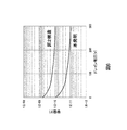
- FIG. 6 shows the capacitance characteristics between the gate and drain when the structure shown in FIG. Compared to the structure of FIG. 2, it can be seen that the gate-drain capacitance is reduced by about one digit in this embodiment.
- the reason why the capacitance between the gate and drain is reduced will be described with reference to FIG.
- the broken line in FIG. 7 indicates the end of the depletion layer at zero bias.
- the channel is completely depleted by the gate regions on both sides, and a depletion layer extends from the trench bottom p region 6.
- the depletion layer extends from the gate region toward the drain region in the structure of FIG. 2, but in this embodiment, the depletion immediately extends from the adjacent trench bottom p region 6.
- the layers are connected and the gate is shielded when viewed from the drain. This reduces the capacitance between the gate and drain.
- the capacitance between the gate and the drain is determined by how the gate can be shielded by the trench bottom p region. Therefore, as the distance from the gate end to the trench bottom increases, the gate is shielded and the capacitance decreases.
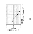
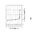
- FIG. 8 shows the relationship between the distance from the gate end to the trench bottom and the gate-drain capacitance. If the distance is less than 0.5 ⁇ m, it is not sufficiently shielded, but a saturation tendency is seen in the range of 0.5 to 1.5 ⁇ m. Therefore, this distance is desirably 0.5 ⁇ m or more. From the above examination, about 0.8 ⁇ m is adopted in this embodiment. There are no significant differences in the breakdown voltage and on-resistance from the conventional structure. However, in the structure of the present invention, in the blocking state, the potential from the drain can be blocked at the trench bottom p region and the potential drop of the channel can be suppressed, so the breakdown voltage may increase depending on the channel conditions.
- the current between the gate and the source also causes the punch-through and the current to flow when the distance from the gate end to the trench bottom is short. It is desirable to take the distance to the bottom. Specifically, since the gate current flows rapidly at a distance of less than 0.5, it is desirable to secure a distance of 0.5 ⁇ m or more.
- the bottom of the p region (p semiconductor layer) formed at the bottom of the trench and short-circuited with the source is sufficiently deep with respect to the bottom of the gate p region, and the gate region is formed by the depletion layer extending from the trench bottom p region.
- the capacitance between the gate and the drain is reduced.
- the gate region and the trench bottom p region are spaced from each other in the direction perpendicular to the substrate surface, the breakdown voltage between the gate and the source can be ensured without increasing the trench width (cell pitch).
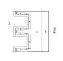
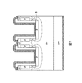
- n ⁇ drift layer (silicon carbide layer) 2 is formed by epitaxial growth on an n + substrate (silicon carbide substrate) 1 serving as a drain region, and p is formed on the drift layer 2 on the surface of the n + source region 3 and the trench 11.
- a gate region 4 is formed. That is, the end of the p gate region 4 on the drift layer side is formed on the substrate surface side with respect to the bottom surface of the trench 11.
- a p region 6 is formed at the bottom of the trench 11, and the p region 6 is electrically separated from the gate region 4 by an n region 5 formed below the trench side wall.
- the n region 5 is not necessarily essential.
- a Schottky contact 14 is formed at the center of the bottom of the trench 11, and the p region 6 is arranged with the Schottky junction interposed therebetween as shown in the figure.
- the figure shows only the active region through which current flows, but a termination region for electric field relaxation is formed around the active region.
- the drain contact region 10 is formed on the back surface, and the source contact region 8 is formed on the front surface, respectively, by ohmic contact. Source contact region 8 and Schottky contact region 14 are electrically connected by source electrode 9.
- the manufacturing method of the second embodiment will be described with reference to FIG.
- the process up to the formation of the n + source region 3 is the same as that shown in FIG. 3A of the first embodiment.
- FIG. 11B amorphal silicon and silicon oxide are laminated, and the silicon oxide 21 and the amorphous silicon 27 are processed by lithography and dry etching.
- FIG. 11C trenches 11 are formed using the same as a hard mask. At this time, in order to keep the channel width constant, the trench should be as vertical as possible. The trench depth is about 1.0 ⁇ m.
- a p region 22 serving as a gate is formed on the side surface of the trench by ion implantation using the trench processing hard mask as it is.
- the ion species was aluminum, the angle of the oblique ion implantation was 25 degrees, and the energy was a multi-stage implantation with a maximum of 100 keV.
- a trench is further dug using the hard mask in the previous process.
- the depth of digging at this time is about 0.8 ⁇ m, and all the p region 22 at the bottom of the trench implanted in all steps is removed.
- this depth is desirably 0.5 ⁇ m or more in order to avoid punch-through similar to that in the first embodiment.
- n-type impurities are obliquely implanted to form an n region 23.
- the ion species was nitrogen and the energy was 50 keV. It is not always necessary to perform oblique implantation of n-type impurities. However, since this oblique implantation has an effect of ensuring electrical isolation between the p region 22 and the p region 6, it is desirable to perform the oblique implantation. In addition, when oblique implantation is performed, if the impurity concentration is too high, there is a problem that the breakdown voltage is lowered.
- a process for forming p regions 6 at both ends of the trench bottom is entered.
- anisotropic etching back is performed by dry etching to form sidewalls 28 on the trench sidewalls. Since the sidewall 28 is later wet etched with hydrofluoric acid, a film such as O 3 -TEOS having a high etching rate is desirable. Further, the width of the sidewall 28 becomes the width of the trench bottom p region 6.
- the silicon oxide was formed under the condition that the silicon oxide remained 500 nm on the plane and 300 nm on the sidewall 28.
- a SiOC film is formed by CVD using siloxane as a precursor. Since this film is formed while reflowing, the flatness is very high, and the step can be filled.
- the SiOC is etched back to leave the SiOC 29 only in the groove.
- the sidewall 28 is etched by wet etching using hydrofluoric acid. At this time, since SiOC is hydrophobic, it is not etched with hydrofluoric acid, and only the sidewalls 28 are removed.
- p-type impurities are ion-implanted using the remaining amorphous silicon 27 and SiOC 29 as hard masks, thereby forming p regions 6 at both ends of the trench bottom.
- the ion species was aluminum and the energy was 80 keV. Thereafter, SiOC 29 is removed by oxygen ashing and hydrofluoric acid treatment, and amorphous silicon 27 is removed by hydrofluoric acid, and activation annealing is performed in an atmosphere of 1650 degrees argon. Thereafter, sacrificial oxidation is performed to remove the damage of the activation annealing. In this embodiment, since a Schottky contact is formed at the bottom of the trench, sacrificial oxidation was performed twice at 1150 degrees for planarizing the substrate.
- the peripheral portion of the device and the gate contact region are covered with a resist by lithography, and the interlayer insulating film 24 is etched back by dry etching.
- the interlayer insulating film 24 is left to be 50 nm so as not to be damaged by dry etching in the region where the Schottky contact is formed.
- the resist is removed by an oxygen asher, and the trench bottom is opened by wet etching with hydrofluoric acid. Since the film thickness of the interlayer insulating film 24 differs between the bottom surface and the side surface of the trench, the interlayer insulating film 24 on the side surface of the trench is left by this hydrofluoric acid treatment.
- titanium, titanium nitride, and aluminum are deposited from below as a Schottky metal and source wiring by sputtering, and a Schottky interface and a source wiring 30 are formed.
- the subsequent steps are the same as in the first embodiment.
- FIG. 12 shows an equivalent circuit of this embodiment.
- the pn diode is built in the bottom of the trench in the first embodiment as well, since the diffusion potential of the SiC pn junction is as high as about 2.8 V, the loss as a body diode is large. Because of the diode, the loss becomes small when the diffusion potential is about 1V.
- the diode of the present embodiment may be molybdenum, nickel or a silicon compound thereof instead of titanium, or a heterojunction diode using polysilicon.
- Example 3 is an example in which the junction FET of the first example of the present invention is mounted on an insulating substrate. This will be described with reference to the bird's eye view of FIG.
- a metal plate of a source terminal 19, a gate terminal 20, and a drain terminal 15 is disposed on an insulating substrate 16 made of aluminum nitride, and a junction FET 17 and a diode 18 are bonded to the drain terminal 15 by soldering.
- the source electrode of the junction FET 17 is bonded to the source terminal 19, the gate electrode is bonded to the gate terminal 20, and the anode of the diode 18 is bonded to the source terminal 19 by wires.
- the diode 18 is a SiC Schottky barrier diode.
- Example 4 is an example of the gate driver circuit of the junction FET of the present invention. This will be described with reference to the circuit diagram of FIG. Two positive and negative power supplies are used. Since the junction FET of the present invention has a low threshold voltage of about 1 V, positive and negative power supplies are used to speed up switching and prevent malfunction. However, there is no problem with a single positive power supply when the noise is small with a small current. Conventionally, since a large current has flown through the gate during switching, the bipolar transistor has been used in two stages. However, in the present invention, the gate current can be kept small, so that the gate driver can be installed in one stage of the bipolar transistor. It is composed.
- Example 5 is a circuit diagram when the junction FET of the present invention is applied to an inverter. This will be described with reference to the circuit diagram of FIG.
- the on-resistance of the element is low, so that the conduction loss can be reduced.
- the switching loss can also be reduced. Loss could be reduced by about 40%.
Landscapes
- Engineering & Computer Science (AREA)
- Microelectronics & Electronic Packaging (AREA)
- Power Engineering (AREA)
- Condensed Matter Physics & Semiconductors (AREA)
- General Physics & Mathematics (AREA)
- Physics & Mathematics (AREA)
- Computer Hardware Design (AREA)
- Ceramic Engineering (AREA)
- Manufacturing & Machinery (AREA)
- Chemical & Material Sciences (AREA)
- Crystallography & Structural Chemistry (AREA)
- Electrodes Of Semiconductors (AREA)
- Junction Field-Effect Transistors (AREA)
- Power Conversion In General (AREA)
Abstract
Dans un TEC de jonction classique de type à tranchée employant un substrat de carbure de silicium, la proportion de la superficie de l'élément occupé par la jonction pn entre la grille et le drain est grande, la capacité entre la grille et le drain est grande, et des problèmes sont associés à ces facteurs. La présente invention concerne donc un TEC de jonction de type à tranchée ayant une capacité réduite entre la grille et le drain, sans diminuer la tension de tenue, sur la résistance, ou les caractéristiques de grille. Spécifiquement, une région p (4) de la grille est formée dans la paroi latérale supérieure d'une tranchée (11). En outre, une région p (6) qui court-circuite la source est formée au niveau du fond de la tranchée. La distance entre cette région p (6) et la région p (4) de la grille s'étend dans une direction perpendiculaire par rapport à la surface du substrat.
Priority Applications (2)
| Application Number | Priority Date | Filing Date | Title |
|---|---|---|---|
| PCT/JP2011/001886 WO2012131768A1 (fr) | 2011-03-30 | 2011-03-30 | Dispositif à semi-conducteur en carbure de silicium et son procédé de production |
| JP2013506829A JP5646044B2 (ja) | 2011-03-30 | 2011-03-30 | 炭化珪素半導体装置およびその製造方法 |
Applications Claiming Priority (1)
| Application Number | Priority Date | Filing Date | Title |
|---|---|---|---|
| PCT/JP2011/001886 WO2012131768A1 (fr) | 2011-03-30 | 2011-03-30 | Dispositif à semi-conducteur en carbure de silicium et son procédé de production |
Publications (1)
| Publication Number | Publication Date |
|---|---|
| WO2012131768A1 true WO2012131768A1 (fr) | 2012-10-04 |
Family
ID=46929620
Family Applications (1)
| Application Number | Title | Priority Date | Filing Date |
|---|---|---|---|
| PCT/JP2011/001886 WO2012131768A1 (fr) | 2011-03-30 | 2011-03-30 | Dispositif à semi-conducteur en carbure de silicium et son procédé de production |
Country Status (2)
| Country | Link |
|---|---|
| JP (1) | JP5646044B2 (fr) |
| WO (1) | WO2012131768A1 (fr) |
Cited By (9)
| Publication number | Priority date | Publication date | Assignee | Title |
|---|---|---|---|---|
| JP2014183259A (ja) * | 2013-03-21 | 2014-09-29 | Renesas Electronics Corp | 半導体装置の製造方法および半導体装置 |
| WO2016042621A1 (fr) * | 2014-09-17 | 2016-03-24 | 株式会社日立製作所 | Dispositif à semi-conducteur, module d'onduleur, onduleur, véhicule ferroviaire, et procédé de fabrication de dispositif à semi-conducteur |
| WO2016080322A1 (fr) * | 2014-11-18 | 2016-05-26 | ローム株式会社 | Dispositif à semi-conducteur et procédé de fabrication de dispositif à semi-conducteur |
| WO2017011425A1 (fr) * | 2015-07-14 | 2017-01-19 | United Silicon Carbide, Inc. | Transistor à effet de champ à jonction vertical et son procédé de fabrication |
| EP3005419A4 (fr) * | 2013-06-06 | 2017-03-15 | United Silicon Carbide Inc. | Jfet connecté à blindage de tranchée |
| US10050154B2 (en) | 2015-07-14 | 2018-08-14 | United Silicon Carbide, Inc. | Trench vertical JFET with ladder termination |
| JP2019531601A (ja) * | 2016-09-09 | 2019-10-31 | ユナイテッド シリコン カーバイド、インク. | 改善された閾値電圧制御を有するトレンチ垂直jfet |
| CN112997294A (zh) * | 2018-11-07 | 2021-06-18 | 株式会社电装 | 半导体装置 |
| US11923716B2 (en) | 2019-09-13 | 2024-03-05 | Milwaukee Electric Tool Corporation | Power converters with wide bandgap semiconductors |
Citations (6)
| Publication number | Priority date | Publication date | Assignee | Title |
|---|---|---|---|---|
| JPH09508492A (ja) * | 1993-12-28 | 1997-08-26 | ノース カロライナ ステート ユニバーシティ | 整流ゲートを有する三端子ゲート制御半導体スイッチング・デバイス |
| JP2003068760A (ja) * | 2001-08-29 | 2003-03-07 | Denso Corp | 炭化珪素半導体装置およびその製造方法 |
| JP2003069042A (ja) * | 2001-08-29 | 2003-03-07 | Denso Corp | 炭化珪素半導体装置及びその製造方法 |
| JP2003318409A (ja) * | 2002-04-23 | 2003-11-07 | Denso Corp | 半導体装置及びその製造方法 |
| JP2004063507A (ja) * | 2002-07-24 | 2004-02-26 | Sumitomo Electric Ind Ltd | 縦型接合型電界効果トランジスタ、及び縦型接合型電界効果トランジスタの製造方法 |
| US20100003573A1 (en) * | 2007-07-18 | 2010-01-07 | Stmicroelectronics S.A. | Method for processing portions of walls of an opening formed in a silicon substrate |
-
2011
- 2011-03-30 JP JP2013506829A patent/JP5646044B2/ja not_active Expired - Fee Related
- 2011-03-30 WO PCT/JP2011/001886 patent/WO2012131768A1/fr active Application Filing
Patent Citations (6)
| Publication number | Priority date | Publication date | Assignee | Title |
|---|---|---|---|---|
| JPH09508492A (ja) * | 1993-12-28 | 1997-08-26 | ノース カロライナ ステート ユニバーシティ | 整流ゲートを有する三端子ゲート制御半導体スイッチング・デバイス |
| JP2003068760A (ja) * | 2001-08-29 | 2003-03-07 | Denso Corp | 炭化珪素半導体装置およびその製造方法 |
| JP2003069042A (ja) * | 2001-08-29 | 2003-03-07 | Denso Corp | 炭化珪素半導体装置及びその製造方法 |
| JP2003318409A (ja) * | 2002-04-23 | 2003-11-07 | Denso Corp | 半導体装置及びその製造方法 |
| JP2004063507A (ja) * | 2002-07-24 | 2004-02-26 | Sumitomo Electric Ind Ltd | 縦型接合型電界効果トランジスタ、及び縦型接合型電界効果トランジスタの製造方法 |
| US20100003573A1 (en) * | 2007-07-18 | 2010-01-07 | Stmicroelectronics S.A. | Method for processing portions of walls of an opening formed in a silicon substrate |
Cited By (20)
| Publication number | Priority date | Publication date | Assignee | Title |
|---|---|---|---|---|
| JP2014183259A (ja) * | 2013-03-21 | 2014-09-29 | Renesas Electronics Corp | 半導体装置の製造方法および半導体装置 |
| EP2782122A3 (fr) * | 2013-03-21 | 2014-12-24 | Renesas Electronics Corporation | Procédé de fabrication de dispositif JFET à semi-conducteur et dispositif JFET à semi-conducteur |
| US9048264B2 (en) | 2013-03-21 | 2015-06-02 | Renesas Electronics Corporation | Manufacturing method of semiconductor device and semiconductor device |
| US9406743B2 (en) | 2013-03-21 | 2016-08-02 | Renesas Electronics Corporation | Semiconductor device with counter doped layer |
| EP3005419A4 (fr) * | 2013-06-06 | 2017-03-15 | United Silicon Carbide Inc. | Jfet connecté à blindage de tranchée |
| WO2016042621A1 (fr) * | 2014-09-17 | 2016-03-24 | 株式会社日立製作所 | Dispositif à semi-conducteur, module d'onduleur, onduleur, véhicule ferroviaire, et procédé de fabrication de dispositif à semi-conducteur |
| JPWO2016042621A1 (ja) * | 2014-09-17 | 2017-04-27 | 株式会社日立製作所 | 半導体装置、インバータモジュール、インバータ、鉄道車両、および半導体装置の製造方法 |
| WO2016080322A1 (fr) * | 2014-11-18 | 2016-05-26 | ローム株式会社 | Dispositif à semi-conducteur et procédé de fabrication de dispositif à semi-conducteur |
| US11189709B2 (en) | 2014-11-18 | 2021-11-30 | Rohm Co., Ltd. | Semiconductor device and method for manufacturing semiconductor device |
| JPWO2016080322A1 (ja) * | 2014-11-18 | 2017-09-14 | ローム株式会社 | 半導体装置および半導体装置の製造方法 |
| US10050154B2 (en) | 2015-07-14 | 2018-08-14 | United Silicon Carbide, Inc. | Trench vertical JFET with ladder termination |
| US10056500B2 (en) | 2015-07-14 | 2018-08-21 | United Silicon Carbide, Inc. | Vertical JFET made using a reduced mask set |
| US10367099B2 (en) | 2015-07-14 | 2019-07-30 | United Silicon Carbide, Inc. | Trench vertical JFET with ladder termination |
| US10367098B2 (en) | 2015-07-14 | 2019-07-30 | United Silicon Carbide, Inc. | Vertical JFET made using a reduced masked set |
| WO2017011425A1 (fr) * | 2015-07-14 | 2017-01-19 | United Silicon Carbide, Inc. | Transistor à effet de champ à jonction vertical et son procédé de fabrication |
| JP2019531601A (ja) * | 2016-09-09 | 2019-10-31 | ユナイテッド シリコン カーバイド、インク. | 改善された閾値電圧制御を有するトレンチ垂直jfet |
| JP7118050B2 (ja) | 2016-09-09 | 2022-08-15 | ユナイテッド シリコン カーバイド、インク. | 改善された閾値電圧制御を有するトレンチ垂直jfet |
| CN112997294A (zh) * | 2018-11-07 | 2021-06-18 | 株式会社电装 | 半导体装置 |
| CN112997294B (zh) * | 2018-11-07 | 2023-10-24 | 株式会社电装 | 半导体装置 |
| US11923716B2 (en) | 2019-09-13 | 2024-03-05 | Milwaukee Electric Tool Corporation | Power converters with wide bandgap semiconductors |
Also Published As
| Publication number | Publication date |
|---|---|
| JP5646044B2 (ja) | 2014-12-24 |
| JPWO2012131768A1 (ja) | 2014-07-24 |
Similar Documents
| Publication | Publication Date | Title |
|---|---|---|
| JP5646044B2 (ja) | 炭化珪素半導体装置およびその製造方法 | |
| JP6049784B2 (ja) | 炭化珪素半導体装置およびその製造方法 | |
| JP5449094B2 (ja) | 半導体装置 | |
| KR101638754B1 (ko) | 반도체 장치 | |
| US9825164B2 (en) | Silicon carbide semiconductor device and manufacturing method for same | |
| JP6109444B1 (ja) | 半導体装置 | |
| JP2016006854A (ja) | 半導体素子およびその製造方法 | |
| US9029874B2 (en) | Semiconductor device having a first silicon carbide semiconductor layer and a second silicon carbide semiconductor layer | |
| WO2013001677A1 (fr) | Dispositif à semi-conducteurs et son procédé de fabrication | |
| EP3005419A1 (fr) | Jfet connecté à blindage de tranchée | |
| JP2018107168A (ja) | 半導体装置および半導体装置の製造方法 | |
| WO2017047286A1 (fr) | Dispositif à semi-conducteur | |
| JPWO2011136272A1 (ja) | 半導体装置 | |
| JPWO2013103051A1 (ja) | 半導体装置 | |
| WO2012063310A1 (fr) | Dispositif à semi-conducteur | |
| CN110291620B (zh) | 半导体装置及半导体装置的制造方法 | |
| JP2023001343A (ja) | 半導体装置 | |
| JP7029711B2 (ja) | 半導体装置 | |
| US7772613B2 (en) | Semiconductor device with large blocking voltage and method of manufacturing the same | |
| CN111512448B (zh) | 半导体装置 | |
| CN112466922A (zh) | 半导体装置 | |
| JP5059989B1 (ja) | 半導体装置とその製造方法 | |
| WO2015111177A1 (fr) | Dispositif à semi-conducteur, module de puissance, dispositif de conversion de puissance et véhicule de chemin de fer | |
| CA3025767A1 (fr) | Dispositif a semi-conducteur | |
| CN112466923A (zh) | 半导体装置 |
Legal Events
| Date | Code | Title | Description |
|---|---|---|---|
| 121 | Ep: the epo has been informed by wipo that ep was designated in this application |
Ref document number: 11862106 Country of ref document: EP Kind code of ref document: A1 |
|
| ENP | Entry into the national phase |
Ref document number: 2013506829 Country of ref document: JP Kind code of ref document: A |
|
| NENP | Non-entry into the national phase |
Ref country code: DE |
|
| 122 | Ep: pct application non-entry in european phase |
Ref document number: 11862106 Country of ref document: EP Kind code of ref document: A1 |