WO2012120968A1 - 電子部品 - Google Patents
電子部品 Download PDFInfo
- Publication number
- WO2012120968A1 WO2012120968A1 PCT/JP2012/053101 JP2012053101W WO2012120968A1 WO 2012120968 A1 WO2012120968 A1 WO 2012120968A1 JP 2012053101 W JP2012053101 W JP 2012053101W WO 2012120968 A1 WO2012120968 A1 WO 2012120968A1
- Authority
- WO
- WIPO (PCT)
- Prior art keywords
- acoustic wave
- main surface
- surface acoustic
- support layer
- wave element
- Prior art date
- Legal status (The legal status is an assumption and is not a legal conclusion. Google has not performed a legal analysis and makes no representation as to the accuracy of the status listed.)
- Ceased
Links
Images





Classifications
-
- H—ELECTRICITY
- H03—ELECTRONIC CIRCUITRY
- H03H—IMPEDANCE NETWORKS, e.g. RESONANT CIRCUITS; RESONATORS
- H03H9/00—Networks comprising electromechanical or electro-acoustic elements; Electromechanical resonators
- H03H9/46—Filters
- H03H9/64—Filters using surface acoustic waves
-
- H—ELECTRICITY
- H03—ELECTRONIC CIRCUITRY
- H03H—IMPEDANCE NETWORKS, e.g. RESONANT CIRCUITS; RESONATORS
- H03H9/00—Networks comprising electromechanical or electro-acoustic elements; Electromechanical resonators
- H03H9/02—Details
- H03H9/05—Holders or supports
- H03H9/058—Holders or supports for surface acoustic wave devices
- H03H9/059—Holders or supports for surface acoustic wave devices consisting of mounting pads or bumps
-
- H—ELECTRICITY
- H03—ELECTRONIC CIRCUITRY
- H03H—IMPEDANCE NETWORKS, e.g. RESONANT CIRCUITS; RESONATORS
- H03H9/00—Networks comprising electromechanical or electro-acoustic elements; Electromechanical resonators
- H03H9/02—Details
- H03H9/05—Holders or supports
- H03H9/10—Mounting in enclosures
- H03H9/1064—Mounting in enclosures for surface acoustic wave [SAW] devices
- H03H9/1085—Mounting in enclosures for surface acoustic wave [SAW] devices the enclosure being defined by a non-uniform sealing mass covering the non-active sides of the SAW device
-
- H—ELECTRICITY
- H03—ELECTRONIC CIRCUITRY
- H03H—IMPEDANCE NETWORKS, e.g. RESONANT CIRCUITS; RESONATORS
- H03H9/00—Networks comprising electromechanical or electro-acoustic elements; Electromechanical resonators
- H03H9/02—Details
- H03H9/05—Holders or supports
- H03H9/10—Mounting in enclosures
- H03H9/1064—Mounting in enclosures for surface acoustic wave [SAW] devices
- H03H9/1092—Mounting in enclosures for surface acoustic wave [SAW] devices the enclosure being defined by a cover cap mounted on an element forming part of the surface acoustic wave [SAW] device on the side of the IDT's
-
- H—ELECTRICITY
- H03—ELECTRONIC CIRCUITRY
- H03H—IMPEDANCE NETWORKS, e.g. RESONANT CIRCUITS; RESONATORS
- H03H9/00—Networks comprising electromechanical or electro-acoustic elements; Electromechanical resonators
- H03H9/46—Filters
- H03H9/64—Filters using surface acoustic waves
- H03H9/6423—Means for obtaining a particular transfer characteristic
- H03H9/6433—Coupled resonator filters
- H03H9/6483—Ladder SAW filters
-
- H—ELECTRICITY
- H10—SEMICONDUCTOR DEVICES; ELECTRIC SOLID-STATE DEVICES NOT OTHERWISE PROVIDED FOR
- H10W—GENERIC PACKAGES, INTERCONNECTIONS, CONNECTORS OR OTHER CONSTRUCTIONAL DETAILS OF DEVICES COVERED BY CLASS H10
- H10W72/00—Interconnections or connectors in packages
- H10W72/01—Manufacture or treatment
- H10W72/012—Manufacture or treatment of bump connectors, dummy bumps or thermal bumps
Definitions
- the present invention relates to an electronic component, and more particularly, to an electronic component including a surface acoustic wave element.
- an acoustic wave device As an electronic component equipped with a conventional surface acoustic wave element, for example, an acoustic wave device described in Patent Document 1 is known.
- an acoustic wave element is provided on a piezoelectric substrate.
- the piezoelectric substrate is covered with a resin film.
- a cavity is provided on the acoustic wave element so that the resin film does not contact the acoustic wave element.
- the elastic wave device described in Patent Document 1 has a problem that the cavity is crushed during mounting. More specifically, when a circuit module including an acoustic wave device is manufactured, the acoustic wave device is mounted on a substrate and then molded with a resin so as to cover the acoustic wave device. At this time, a relatively high pressure is applied to the resin. Therefore, in the acoustic wave device described in Patent Document 1, the resin film may be deformed by pressure, and the hollow portion may be crushed. In particular, as the volume of the cavity increases, the cavity tends to collapse.
- an object of the present invention is to provide an electronic component that can suppress the collapse of the space provided on the surface acoustic wave device.
- An electronic component includes a substrate, a support layer surrounding a predetermined region on the main surface when viewed in a plan view from a normal direction of the main surface of the substrate, and the predetermined region.
- the cover layer provided on the support layer and facing the main surface, and the main surface, the support layer and the cover layer And a columnar member that connects the main surface and the cover layer and is not in contact with the support layer.
- FIG. 2 is a cross-sectional structural view taken along the line AA of the SAW filter of FIG. It is an exploded view of the SAW filter of FIG.
- FIG. 2 is an equivalent circuit diagram of the SAW filter of FIG. 1.
- It is a cross-sectional structure diagram of a circuit module on which a SAW filter is mounted. It is process sectional drawing at the time of manufacture of a SAW filter. It is process sectional drawing at the time of manufacture of a SAW filter.
- It is a sectional structure figure of a SAW filter concerning the 1st modification.
- It is a cross-section figure of a SAW filter concerning the 2nd modification.
- SAW surface acoustic wave
- FIG. 1 is a plan view of the SAW filter 10.
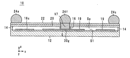
- FIG. 2 is a cross-sectional structural view taken along the line AA of the SAW filter 10 of FIG.
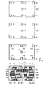
- FIG. 3 is an exploded view of the SAW filter 10 of FIG.
- FIG. 4 is an equivalent circuit diagram of the SAW filter 10 of FIG.
- the stacking direction (vertical direction) of the SAW filter 10 is defined as the z-axis direction.
- the direction along the long side of the SAW filter 10 is defined as the x-axis direction
- the direction along the short side of the SAW filter 10 is defined as the y-axis direction.
- the SAW filter 10 includes a piezoelectric substrate 12, a support layer 14, a columnar member 16, surface acoustic wave elements 18 (18a to 18t), wirings 19, cover layers 20 and 22, bumps (external).
- a connecting portion) 24 (24a to 24g), pads 30 (30a to 30g), and via-hole conductors V1 to V7.
- the piezoelectric substrate 12 has a rectangular plate shape and has a main surface S1 (see FIG. 2).
- a quartz substrate, a LiTaO 3 substrate, a LiNbO 3 substrate, a substrate on which a ZnO thin film is formed, or the like is used as the piezoelectric substrate 12.
- the main surface S ⁇ b> 1 indicates a main surface located on the positive side in the z-axis direction of the two main surfaces of the piezoelectric substrate 12.
- the element region E is a region excluding the vicinity of the corner and the vicinity of each side in the main surface S1.
- the support layer 14 has a rectangular frame shape surrounding the element region E when viewed in plan from the z-axis direction. More specifically, as shown in FIG. 3, the support layer 14 includes a frame portion 14a and protrusions 14b to 14g.
- the frame portion 14a has a rectangular frame shape along the four sides of the main surface S1.
- Each of the protrusions 14b to 14e protrudes toward the inside of the frame part 14a at the four corners of the main surface S1.
- the projecting portions 14f and 14g project toward the inside of the frame portion 14a at the midpoints of the long sides of the main surface S1 on the positive and negative sides in the y-axis direction.
- the support layer 14 serves to prevent moisture and the like from entering the SAW filter 10, and is made of an insulating material (for example, polyimide) having excellent water resistance.
- the element region E means a region where the support layer 14 is not provided in the main surface S1.
- the cover layer 20 is provided on the positive side of the support layer 14 in the z-axis direction and faces the main surface S1. More specifically, the cover layer 20 has substantially the same rectangular shape as the main surface S1.
- the cover layer 20 is stacked on the positive side of the support layer 14 in the z-axis direction, so that the cover layer 20 is opposed to the main surface S1 through a space.
- a space surrounded by the main surface on the negative direction side in the z-axis direction of the main surface S1, the support layer 14, and the cover layer 20 is referred to as a space Sp.
- the cover layer 20 is made of an insulating material different from that of the support layer 14, and is made of, for example, epoxy.
- the cover layer 22 is provided on the positive side of the z-axis direction of the cover layer 20 as shown in FIG. More specifically, the cover layer 22 has the same rectangular shape as the cover layer 20, and overlaps with the cover layer 20 when viewed in plan from the z-axis direction.
- the cover layer 22 plays a role of preventing moisture and the like from entering the SAW filter 10 and is made of an insulating material (for example, polyimide) having excellent water resistance. That is, the cover layer 22 is made of the same insulating material as the support layer 14.
- the cover layer 22 is formed after the support layer 14 is cured, when the cover layer 22 is directly laminated on the support layer 14, the cover layer 22 is difficult to adhere to the support layer 14. Therefore, in the SAW filter 10, the cover layer 20 is provided between the support layer 14 and the cover layer 22. That is, the cover layer 20 bonds the support layer 14 and the cover layer 22 together.
- the columnar member 16 connects the main surface S1 and the main surface on the negative side in the z-axis direction of the cover layer 20 in the space Sp and is not in contact with the support layer 14. More specifically, the columnar member 16 is provided near the intersection of diagonal lines of the main surface S1 (that is, near the center of the main surface S1) when viewed in plan from the positive direction side in the z-axis direction. It is a cylindrical insulator extending in the direction.
- the columnar member 16 is made of the same insulating material (that is, polyimide) as the support layer 14. The columnar member 16 prevents the cover layers 20 and 22 from being deformed and the space Sp from being crushed.
- Each of the pads 30a to 30f is made of a conductor layer such as Al, Cu, Ni, Au, or Pt provided on the main surface S1, and when viewed in a plan view from the z-axis direction as shown in FIGS.
- the protrusions 14b to 14g of the support layer 14 overlap.
- Via holes conductors V1 to V6 described later are connected to the pads 30a to 30f.
- the pad 30g is made of a conductor layer such as Al, Cu, Ni, Au, and Pt provided on the main surface S1, and as shown in FIG. It overlaps with the intersection of the diagonals.
- a via hole conductor V7 described later is connected to the pad 30g.
- each of the via-hole conductors V1 to V6 penetrates the support layer 14 and the cover layers 20 and 22 in the z-axis direction. Ends on the negative side in the z-axis direction of the via-hole conductors V1 to V6 are connected to pads 30a to 30f, respectively.
- the via-hole conductor V7 penetrates the columnar member 16 and the cover layers 20 and 22 in the z-axis direction. That is, the via-hole conductor V7 extends in the z-axis direction (normal direction of the main surface S1) in the columnar member 16. The end of the via-hole conductor V7 on the negative side in the z-axis direction is connected to the pad 30g.
- the bumps 24a to 24g are provided on the main surface on the positive side in the z-axis direction of the cover layer 22 immediately above the via-hole conductors V1 to V7, respectively. Connected to the end.
- the bump 24f corresponds to an external connection portion.
- the bumps 24a to 24g are connected to the land of the circuit board when the SAW filter 10 is mounted on the circuit board, and are, for example, spherical solder.
- the surface acoustic wave element 18 is provided in the element region E.
- the surface acoustic wave element 18 is made of a conductor layer made of Al, Cu, Ni, Au, Pt or the like formed on the main surface S1 to form an IDT (Inter Digital Transducer) by facing two comb electrodes. Yes.
- the surface acoustic wave element 18 constitutes a resonator having resonance characteristics with a resonance frequency determined by the pitch of the comb electrodes.
- a ladder type filter having a ladder type circuit is constituted by the plurality of surface acoustic wave elements 18.
- the surface acoustic wave elements 18 having different sizes are provided so that the ladder filter has a desired pass characteristic.
- the configuration and principle of the surface acoustic wave element 18 are the same as the configuration and principle of a general surface acoustic wave element, and a detailed description thereof will be omitted.
- the wiring 19 is made of a conductive layer made of Al, Cu, Ni, Au, Pt or the like formed on the main surface S1, and connects the surface acoustic wave element 18 and the pad 30.
- a conductive layer made of Al, Cu, Ni, Au, Pt or the like formed on the main surface S1, and connects the surface acoustic wave element 18 and the pad 30.
- the surface acoustic wave elements 18a to 18f are connected in series between the bump 24a and the bump 24b as shown in FIG. More specifically, one comb electrode of the surface acoustic wave element 18a is connected to the bump 24a via the wiring 19, the pad 30a, and the via-hole conductor V1. The other comb-shaped electrode of the surface acoustic wave element 18 a is connected to one comb-shaped electrode of the surface acoustic wave element 18 b through the wiring 19. The other comb-shaped electrode of the surface acoustic wave element 18 b is connected to one comb-shaped electrode of the surface acoustic wave element 18 c through the wiring 19.
- the other comb-shaped electrode of the surface acoustic wave element 18 c is connected to one comb-shaped electrode of the surface acoustic wave element 18 d through the wiring 19.
- the other comb-shaped electrode of the surface acoustic wave element 18 d is connected to one comb-shaped electrode of the surface acoustic wave element 18 e through the wiring 19.
- the other comb-shaped electrode of the surface acoustic wave element 18 e is connected to one comb-shaped electrode of the surface acoustic wave element 18 f through the wiring 19.
- the other comb-shaped electrode of the surface acoustic wave element 18f is connected to the bump 24b through the wiring 19, the pad 30b, and the via-hole conductor V2.
- the surface acoustic wave element 18g is connected between the bump 24a and the bump 24e as shown in FIG. More specifically, one comb electrode of the surface acoustic wave element 18g is connected to the bump 24a via the wiring 19, the pad 30a, and the via-hole conductor V1. The other comb-shaped electrode of the surface acoustic wave element 18g is connected to the bump 24e via the wiring 19, the pad 30e, and the via-hole conductor V5.
- the surface acoustic wave element 18h is connected between the surface acoustic wave elements 18b and 18c and the bump 24e as shown in FIG. More specifically, one comb electrode of the surface acoustic wave element 18 h is connected to the other comb electrode of the surface acoustic wave element 18 b and one comb electrode of the surface acoustic wave element 18 c via the wiring 19. The other comb-shaped electrode of the surface acoustic wave element 18h is connected to the bump 24e via the wiring 19, the pad 30e, and the via-hole conductor V5.
- the surface acoustic wave element 18i is connected between the surface acoustic wave elements 18d and 18e and the bumps 24g and 24f as shown in FIG. More specifically, one comb electrode of the surface acoustic wave element 18 i is connected to the other comb electrode of the surface acoustic wave element 18 d and one comb electrode of the surface acoustic wave element 18 e via the wiring 19. The other comb electrode of the surface acoustic wave element 18i is connected to the bump 24g via the wiring 19, the pad 30g and the via hole conductor V7, and is connected to the bump 24f via the wiring 19, the pad 30f and the via hole conductor V6. ing.
- the surface acoustic wave element 18j is connected between the bump 24b and the bumps 24g and 24f. More specifically, one comb-shaped electrode of the surface acoustic wave element 18j is connected to the bump 24b via the wiring 19, the pad 30b, and the via-hole conductor V2. The other comb electrode of the surface acoustic wave element 18j is connected to the bump 24g via the wiring 19, the pad 30g and the via hole conductor V7, and is connected to the bump 24f via the wiring 19, the pad 30f and the via hole conductor V6. ing.
- the surface acoustic wave elements 18k to 18p are connected in series between the bump 24c and the bump 24d as shown in FIG. More specifically, one comb-shaped electrode of the surface acoustic wave element 18k is connected to the bump 24c via the wiring 19, the pad 30c, and the via-hole conductor V3. The other comb-shaped electrode of the surface acoustic wave element 18 k is connected to one comb-shaped electrode of the surface acoustic wave element 18 l via the wiring 19. The other comb-shaped electrode of the surface acoustic wave element 18l is connected to one comb-shaped electrode of the surface acoustic wave element 18m via the wiring 19.
- the other comb-shaped electrode of the surface acoustic wave element 18m is connected to one comb-shaped electrode of the surface acoustic wave element 18n via the wiring 19.
- the other comb-shaped electrode of the surface acoustic wave element 18 n is connected to one comb-shaped electrode of the surface acoustic wave element 18 o via the wiring 19.
- the other comb-shaped electrode of the surface acoustic wave element 18 o is connected to one comb-shaped electrode of the surface acoustic wave element 18 p through the wiring 19.
- the other comb-shaped electrode of the surface acoustic wave element 18p is connected to the bump 24d through the wiring 19, the pad 30d, and the via-hole conductor V4.
- the surface acoustic wave element 18q is connected between the bump 24c and the bump 24e as shown in FIG. More specifically, one comb electrode of the surface acoustic wave element 18q is connected to the bump 24c via the wiring 19, the pad 30c, and the via-hole conductor V3. The other comb-shaped electrode of the surface acoustic wave element 18q is connected to the bump 24e via the wiring 19, the pad 30e, and the via-hole conductor V5.
- the surface acoustic wave element 18r is connected between the surface acoustic wave elements 18l and 18m and the bump 24e as shown in FIG. More specifically, one comb electrode of the surface acoustic wave element 18r is connected to the other comb electrode of the surface acoustic wave element 18l and one comb electrode of the surface acoustic wave element 18m via the wiring 19. The other comb-shaped electrode of the surface acoustic wave element 18r is connected to the bump 24e via the wiring 19, the pad 30e, and the via-hole conductor V5.
- the surface acoustic wave element 18s is connected between the surface acoustic wave elements 18n and 18o and the bumps 24g and 24f as shown in FIG. More specifically, one comb electrode of the surface acoustic wave element 18 s is connected to the other comb electrode of the surface acoustic wave element 18 n and one comb electrode of the surface acoustic wave element 18 o via the wiring 19. The other comb-shaped electrode of the surface acoustic wave element 18s is connected to the bump 24g via the wiring 19, the pad 30g and the via-hole conductor V7, and is connected to the bump 24f via the wiring 19, the pad 30f and the via-hole conductor V6. ing.
- the surface acoustic wave element 18t is connected between the bump 24d and the bumps 24g and 24f. More specifically, one comb electrode of the surface acoustic wave element 18t is connected to the bump 24d through the wiring 19, the pad 30d, and the via-hole conductor V4. The other comb-shaped electrode of the surface acoustic wave element 18t is connected to the bump 24g via the wiring 19, the pad 30g and the via-hole conductor V7, and is connected to the bump 24f via the wiring 19, the pad 30f and the via-hole conductor V6. ing.
- the bump 24a is used as an input terminal for a 900 MHz band high frequency signal
- the bump 24b is used as an output terminal for a 900 MHz band high frequency signal.
- the bumps 24e to 24g are grounded. Accordingly, the surface acoustic wave elements 18a to 18j function as SAW filters that allow high-frequency signals in the 900 MHz band to pass.
- the bump 24c is used as an input terminal for a high frequency signal in the 850 MHz band
- the bump 24d is used as an output terminal for a high frequency signal in the 850 MHz band.
- the bumps 24e to 24g are grounded.
- the surface acoustic wave elements 18k to 18t function as SAW filters that pass high-frequency signals in the 850 MHz band.
- FIG. 5 is a cross-sectional structure diagram of the circuit module 100 on which the SAW filter 10 is mounted.
- the circuit module 100 includes a SAW filter 10, a circuit board 102, a land 104, and a mold resin 106.
- the circuit board 102 is a multilayer wiring board.
- the land 104 is an external electrode provided on the main surface of the circuit board 102.
- the SAW filter 10 is mounted on the circuit board 102 so that the bumps 24 are in contact with the lands 104.
- the bump 24 is spread on the land 104 by being melted at the time of mounting. Thereby, the SAW filter 10 is fixed on the circuit board 102.
- the mold resin 106 covers the main surfaces of the SAW filter 10 and the circuit board 102. Thereby, the SAW filter 10 is protected.
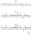
- FIG. 6 and 7 are process cross-sectional views when the SAW filter 10 is manufactured.
- a method for manufacturing one SAW filter 10 will be described.
- a plurality of SAW filters 10 arranged in a matrix are manufactured at the same time, and finally divided into individual SAW filters 10.
- the piezoelectric substrate 12 is prepared.
- the surface acoustic wave element 18, the wiring 19, and the pad 30 are formed on the main surface S1 of the piezoelectric substrate 12 by a photolithography method. Specifically, a resist pattern having an opening is formed in a portion where the surface acoustic wave element 18, the wiring 19, and the pad 30 are formed. Next, a metal having Al as a main component is deposited on the resist pattern and the openings. Next, the resist pattern is removed by dipping in a stripping solution. At this time, the metal film on the resist pattern is also removed. Thereby, the surface acoustic wave element 18, the wiring 19, and the pad 30 are formed on the main surface S1.
- the support layer 14 and the columnar member 16 are formed on the main surface S1 of the piezoelectric substrate 12 by a photolithography method. Specifically, photosensitive polyimide is applied on the main surface S1 of the piezoelectric substrate 12 by spin coating. Next, the photosensitive polyimide is exposed and developed. Further, the photosensitive polyimide is cured by heating, and organic substances adhering to the surface acoustic wave element 18 are removed by oxygen plasma. Thereby, the support layer 14 and the columnar member 16 are formed.
- cover layers 20 and 22 are formed on the support layer 14. Specifically, a laminated film in which a cover layer 20 made of an epoxy film and a cover layer 22 made of a polyimide film are laminated is prepared. Then, the laminated film is placed on the support layer 14 and thermocompression bonded.
- a beam is irradiated to the positions where the via-hole conductors V1 to V7 are formed to form via holes in the support layer 14, the columnar member 16, and the cover layers 20 and 22.
- the method for forming the via hole is not limited to the beam irradiation method, and may be a photolithography method.
- via hole conductors V1 to V7 are formed by filling the inside of the via hole with a conductor by electroplating.
- the periphery of the via-hole conductors V1 to V7 is surrounded by the support layer 14, it is possible to prevent the plating solution from entering the space Sp.
- bumps 24a to 24g are formed by printing solder paste on the via-hole conductors V1 to V7.
- the SAW filter 10 is completed through the above steps.
- the manufacturing method of the SAW filter 10 is an example, the SAW filter 10 may be manufactured by another method.
- the space Sp provided on the surface acoustic wave element 18 can be prevented from being crushed. More specifically, when the circuit module including the acoustic wave device described in Patent Document 1 is manufactured, the acoustic wave device is mounted on a substrate, and then molded with a resin so as to cover the acoustic wave device. The At this time, a relatively high pressure is applied to the resin. Therefore, in the acoustic wave device described in Patent Document 1, the resin film may be deformed by pressure, and the hollow portion may be crushed. In particular, as the volume of the cavity increases, the cavity tends to collapse.
- the SAW filter 10 is provided with a columnar member 16 that connects the main surface S ⁇ b> 1 and the main surface on the negative side of the z-axis direction of the cover layer 20 in the space Sp. .
- the cover layers 20 and 22 are supported by the columnar member 16, so that deformation is suppressed.
- the space Sp is prevented from being crushed.
- the SAW filter 10 has a high degree of design freedom. More specifically, in the SAW filter 10, the columnar member 16 is not in contact with the support layer 14. That is, the columnar member 16 can be disposed at a position away from the support layer 14 in the element region E. Therefore, the columnar member 16 can be arranged at an arbitrary position in the element region E. Therefore, the columnar member 16 can be disposed at a position where the surface acoustic wave element 18, the wiring 19, and the pad 30 are not provided in the element region E. As a result, the SAW filter 10 has a high degree of design freedom.
- the SAW filter 10 provides high heat dissipation. More specifically, the SAW filter 10 is provided with a via-hole conductor V7 that penetrates the columnar member 16 and the cover layers 20 and 22 in the z-axis direction. Furthermore, the via-hole conductor V7 is connected to the wiring 19 through the pad 30g. Therefore, the heat generated by the application of the RF voltage to the SAW filter 10 is radiated to the outside of the SAW filter 10 through the via hole conductor V7. As a result, the SAW filter 10 can improve power durability.
- the SAW filter 10 the attenuation characteristics between the bumps 24a and 24b, the bumps 24c and the bumps 24d, the bumps 24a and the bumps 24 other than the bumps 24b, and the bumps 24c and the bumps 24d other than the bumps 24d. Isolation characteristics between the two are improved. More specifically, the via-hole conductor V7 is connected to the bump 24f to which the ground potential is applied. Thereby, compared with the case where the via-hole conductor V7 is not provided, the SAW filter 10 has more portions to which the ground potential is applied. As a result, the SAW filter 10 has improved attenuation characteristics and isolation characteristics. In particular, when the SAW filter 10 is used in a mobile phone, the isolation characteristic between transmission and reception is improved in the duplexer circuit of the mobile phone.
- the occurrence of ripple can be suppressed. More specifically, in the SAW filter 10, vibration in the z-axis direction is generated and becomes a ripple. On the other hand, the SAW filter 10 is covered with the mold resin 106 in the circuit module 100. Therefore, the vibration in the z-axis direction is absorbed by the mold resin 106. As a result, the occurrence of ripple is suppressed.
- the via-hole conductor V7 and the bump 24f are directly connected, so that wiring for connecting them is not used. As a result, generation of an inductance component and a capacitor component due to the wiring is suppressed, and characteristic deterioration of the SAW filter 10 is suppressed.
- FIG. 8 is a cross-sectional structure diagram of the SAW filter 10a according to the first modification.
- the bumps 24f may not be provided. Also in the SAW filter 10a, the collapse of the space Sp can be suppressed and high heat dissipation can be obtained.
- FIG. 9 is a cross-sectional structure diagram of a SAW filter 10b according to a second modification.
- the bump 24f and the via-hole conductor V7 may not be provided. Also in the SAW filter 10b, the collapse of the space Sp can be suppressed.
- the SAW filter according to the present invention is not limited to the SAW filters 10, 10a, and 10b shown in the above embodiment, and can be modified within the scope of the gist thereof.
- a plurality of columnar members 16 may be provided.
- the columnar member 16 has a cylindrical shape, but may have a prismatic shape or the like.
- the cross-sectional area in the plane parallel to the main surface S1 of the via-hole conductor V7 is preferably larger than the cross-sectional area in the plane parallel to the main surface of the via-hole conductors V1 to V6.
- the via-hole conductor V7 is a via-hole conductor having the greatest heat dissipation effect and grounding effect. Therefore, by increasing the cross-sectional area of the via-hole conductor V7, the heat dissipation effect and the grounding effect can be improved. Furthermore, since the cross-sectional area of the via-hole conductor V7 increases, the space Sp is more effectively suppressed.
- the present invention is useful for electronic components, and is particularly excellent in that the space provided on the surface acoustic wave device can be prevented from being crushed.
Landscapes
- Physics & Mathematics (AREA)
- Acoustics & Sound (AREA)
- Surface Acoustic Wave Elements And Circuit Networks Thereof (AREA)
Abstract
Description
まず、SAWフィルタの構成について図面を参照しながら説明する。図1は、SAWフィルタ10を平面視した図である。図2は、図1のSAWフィルタ10のA-Aにおける断面構造図である。図3は、図1のSAWフィルタ10の分解図である。図4は、図1のSAWフィルタ10の等価回路図である。以下では、SAWフィルタ10の積層方向(鉛直方向)をz軸方向と定義する。また、SAWフィルタ10をz軸方向から平面視したときに、SAWフィルタ10の長辺に沿った方向をx軸方向と定義し、SAWフィルタ10の短辺に沿った方向をy軸方向と定義する。
以下に、SAWフィルタ10の製造方法について図面を参照しながら説明する。図6及び図7は、SAWフィルタ10の製造時の工程断面図である。なお、以下では、1つのSAWフィルタ10の製造方法について説明するが、実際には、マトリクス状に配列された複数のSAWフィルタ10が同時に作製されて、最終的に個別のSAWフィルタ10に分割される。
以上のように構成されたSAWフィルタ10によれば、表面弾性波素子18上に設けられている空間Spがつぶれることを抑制できる。より詳細には、特許文献1に記載の弾性波デバイスを備えた回路モジュールの作製の際には、弾性波デバイスが基板に実装された後に、弾性波デバイスを覆うように樹脂によりモールドが施される。この際、樹脂に対して比較的に高い圧力が加えられる。そのため、特許文献1に記載の弾性波デバイスでは、圧力によって樹脂膜が変形し、空洞部がつぶれるおそれがある。特に、空洞部の体積が大きくなるにしたがって、該空洞部はつぶれやすくなる。
以下に第1の変形例に係るSAWフィルタについて図面を参照しながら説明する。図8は、第1の変形例に係るSAWフィルタ10aの断面構造図である。
以下に第2の変形例に係るSAWフィルタについて図面を参照しながら説明する。図9は、第2の変形例に係るSAWフィルタ10bの断面構造図である。
本発明に係るSAWフィルタは、前記実施形態に示したSAWフィルタ10,10a,10bに限らずその要旨の範囲内において変形可能である。
S1 主面
V1~V7 ビアホール導体
10,10a,10b SAWフィルタ
12 圧電基板
14 支持層
14a 枠部
14b~14g 突起部
16 柱状部材
18a~18t 表面弾性波素子
19 配線
20,22 カバー層
24a~24g バンプ
30a~30g パッド
100 回路モジュール
102 回路基板
104 ランド
106 モールド樹脂
Claims (10)
- 基板と、
前記基板の主面の法線方向から平面視したときに、該主面上の所定領域を囲んでいる支持層と、
前記所定領域内に設けられている表面弾性波素子と、
前記支持層上に設けられ、かつ、前記主面に対向しているカバー層と、
前記主面、前記支持層及び前記カバー層に囲まれた空間内において、該主面と該カバー層とを繋いでいると共に、前記支持層と接触していない柱状部材と、
を備えていること、
を特徴とする電子部品。 - 前記柱状部材内を前記主面の法線方向に延在している第1のビアホール導体を、
更に備えていること、
を特徴とする請求項1に記載の電子部品。 - 前記第1のビアホール導体に接続され、かつ、前記主面上に設けられている配線と、
前記第1のビアホール導体に接続され、かつ、前記第1のビアホール導体の直上の前記カバー層上に設けられている外部接続部であって、接地電位が印加される外部接続部と、
を更に備えていること、
を特徴とする請求項2に記載の電子部品。 - 前記支持層と前記柱状部材とは同じ材料により作製されていること、
を特徴とする請求項1ないし請求項3のいずれかに記載の電子部品。 - 前記カバー層は、
前記支持層上に設けられ、かつ、該支持層とは異なる材料により作製されている第1のカバー層と、
前記第1のカバー層上に設けられ、かつ、前記支持層と同じ材料により作製されている第2のカバー層と、
を含んでいること、
を特徴とする請求項1ないし請求項4のいずれかに記載の電子部品。 - 前記第1のカバー層は、前記支持層と前記第2のカバー層とを接着していること、
を特徴とする請求項5に記載の電子部品。 - 前記表面弾性波素子は、表面弾性波フィルタを構成していること、
を特徴とする請求項1ないし請求項6のいずれかに記載の電子部品。 - 前記所定領域内には、複数の前記表面弾性波素子が設けられていること、
を特徴とする請求項1ないし請求項7のいずれかに記載の電子部品。 - 前記柱状部材は、前記主面の中央に設けられていること、
を特徴とする請求項1ないし請求項8のいずれかに記載の電子部品。 - 前記柱状部材内を前記主面の法線方向に延在している第1のビアホール導体と、
前記支持層内を前記主面の法線方向に延在する第2のビアホール導体と、
更に備え、
前記第1のビアホール導体の前記主面に平行な面における断面積は、前記第2のビアホール導体の該主面に平行な面における断面積よりも大きいこと、
を特徴とする請求項9に記載の電子部品。
Priority Applications (4)
| Application Number | Priority Date | Filing Date | Title |
|---|---|---|---|
| CN201280012133.XA CN103415995B (zh) | 2011-03-09 | 2012-02-10 | 电子元器件 |
| JP2013503428A JP5660197B2 (ja) | 2011-03-09 | 2012-02-10 | 電子部品 |
| DE112012001150.3T DE112012001150B4 (de) | 2011-03-09 | 2012-02-10 | Elektronische Komponente |
| US14/014,839 US9197192B2 (en) | 2011-03-09 | 2013-08-30 | Electronic component including a surface acoustic wave element and a pillar member |
Applications Claiming Priority (2)
| Application Number | Priority Date | Filing Date | Title |
|---|---|---|---|
| JP2011051122 | 2011-03-09 | ||
| JP2011-051122 | 2011-03-09 |
Related Child Applications (1)
| Application Number | Title | Priority Date | Filing Date |
|---|---|---|---|
| US14/014,839 Continuation US9197192B2 (en) | 2011-03-09 | 2013-08-30 | Electronic component including a surface acoustic wave element and a pillar member |
Publications (1)
| Publication Number | Publication Date |
|---|---|
| WO2012120968A1 true WO2012120968A1 (ja) | 2012-09-13 |
Family
ID=46797938
Family Applications (1)
| Application Number | Title | Priority Date | Filing Date |
|---|---|---|---|
| PCT/JP2012/053101 Ceased WO2012120968A1 (ja) | 2011-03-09 | 2012-02-10 | 電子部品 |
Country Status (5)
| Country | Link |
|---|---|
| US (1) | US9197192B2 (ja) |
| JP (1) | JP5660197B2 (ja) |
| CN (1) | CN103415995B (ja) |
| DE (1) | DE112012001150B4 (ja) |
| WO (1) | WO2012120968A1 (ja) |
Cited By (7)
| Publication number | Priority date | Publication date | Assignee | Title |
|---|---|---|---|---|
| WO2014077239A1 (ja) * | 2012-11-13 | 2014-05-22 | 株式会社村田製作所 | 弾性波装置 |
| CN104079261A (zh) * | 2013-03-29 | 2014-10-01 | 精工爱普生株式会社 | 电子器件、电子设备、移动体及电子器件的制造方法 |
| JP2015162804A (ja) * | 2014-02-27 | 2015-09-07 | 株式会社村田製作所 | 電子部品及び電子部品の製造方法 |
| WO2016013330A1 (ja) * | 2014-07-22 | 2016-01-28 | 株式会社村田製作所 | デュプレクサ |
| JP2017011558A (ja) * | 2015-06-24 | 2017-01-12 | 株式会社村田製作所 | 弾性波装置 |
| WO2019044178A1 (ja) * | 2017-08-31 | 2019-03-07 | 株式会社村田製作所 | 弾性波装置およびそれを備えた弾性波モジュール |
| CN118337173A (zh) * | 2024-04-30 | 2024-07-12 | 泉州市三安集成电路有限公司 | 一种弹性波装置、芯片封装方法及射频模块 |
Families Citing this family (12)
| Publication number | Priority date | Publication date | Assignee | Title |
|---|---|---|---|---|
| KR101645172B1 (ko) * | 2012-09-25 | 2016-08-03 | 가부시키가이샤 무라타 세이사쿠쇼 | 탄성파 장치 및 그 제조 방법 |
| KR101754193B1 (ko) * | 2013-08-02 | 2017-07-05 | 가부시키가이샤 무라타 세이사쿠쇼 | 분파장치 |
| KR101754200B1 (ko) * | 2013-08-20 | 2017-07-05 | 가부시키가이샤 무라타 세이사쿠쇼 | 탄성 표면파 디바이스 및 그 제조 방법 |
| KR101931508B1 (ko) * | 2015-03-27 | 2018-12-21 | 가부시키가이샤 무라타 세이사쿠쇼 | 탄성파 장치, 통신 모듈 기기 및 탄성파 장치의 제조 방법 |
| WO2016208287A1 (ja) * | 2015-06-24 | 2016-12-29 | 株式会社村田製作所 | 弾性波フィルタ装置 |
| JP6365436B2 (ja) * | 2015-06-24 | 2018-08-01 | 株式会社村田製作所 | 弾性波装置 |
| JP6350510B2 (ja) * | 2015-12-24 | 2018-07-04 | 株式会社村田製作所 | 弾性表面波装置 |
| WO2017221953A1 (ja) * | 2016-06-21 | 2017-12-28 | 株式会社村田製作所 | 弾性波デバイス |
| US10109903B2 (en) * | 2016-10-06 | 2018-10-23 | Invensas Corporation | Flipped RF filters and components |
| KR20180064175A (ko) | 2016-12-05 | 2018-06-14 | 삼성전기주식회사 | 탄성파 필터 장치 |
| WO2018163841A1 (ja) * | 2017-03-09 | 2018-09-13 | 株式会社村田製作所 | 弾性波装置、弾性波装置パッケージ、マルチプレクサ、高周波フロントエンド回路及び通信装置 |
| KR102188872B1 (ko) * | 2017-12-27 | 2020-12-11 | 가부시키가이샤 무라타 세이사쿠쇼 | 탄성파 필터, 멀티플렉서, 고주파 프론트 엔드 회로 및 통신 장치 |
Citations (6)
| Publication number | Priority date | Publication date | Assignee | Title |
|---|---|---|---|---|
| JP2001094390A (ja) * | 1999-09-20 | 2001-04-06 | Toshiba Corp | 弾性表面波デバイスおよびその製造方法 |
| JP2004129223A (ja) * | 2002-07-31 | 2004-04-22 | Murata Mfg Co Ltd | 圧電部品およびその製造方法 |
| JP2009218762A (ja) * | 2008-03-10 | 2009-09-24 | Panasonic Corp | 弾性表面波デバイス |
| JP2009278016A (ja) * | 2008-05-16 | 2009-11-26 | Kyocera Corp | 電子部品 |
| JP2010245704A (ja) * | 2009-04-02 | 2010-10-28 | Sumitomo Bakelite Co Ltd | 弾性表面波素子用基板および弾性表面波装置 |
| JP2010278972A (ja) * | 2009-06-01 | 2010-12-09 | Murata Mfg Co Ltd | 弾性波装置 |
Family Cites Families (18)
| Publication number | Priority date | Publication date | Assignee | Title |
|---|---|---|---|---|
| US4965479A (en) * | 1987-01-12 | 1990-10-23 | Hewlett-Packard Company | Surface transverse wave resonator |
| CN1099158C (zh) * | 1994-05-02 | 2003-01-15 | 埃普科斯股份有限公司 | 电子部件的封闭装置 |
| JP4377500B2 (ja) | 1999-12-24 | 2009-12-02 | 京セラ株式会社 | 弾性表面波装置及び弾性表面波装置の製造方法 |
| DE10253163B4 (de) * | 2002-11-14 | 2015-07-23 | Epcos Ag | Bauelement mit hermetischer Verkapselung und Waferscale Verfahren zur Herstellung |
| JP4576849B2 (ja) * | 2004-03-01 | 2010-11-10 | パナソニック株式会社 | 集積回路装置 |
| US7298231B2 (en) * | 2004-05-27 | 2007-11-20 | Kyocera Corporation | Surface acoustic wave device and communication apparatus |
| JP4714214B2 (ja) * | 2005-04-01 | 2011-06-29 | パナソニック株式会社 | 弾性表面波デバイス |
| DE102005026243B4 (de) * | 2005-06-07 | 2018-04-05 | Snaptrack, Inc. | Elektrisches Bauelement und Herstellungsverfahren |
| EP1892831B1 (en) | 2005-06-16 | 2012-08-29 | Murata Manufacturing Co., Ltd. | Piezoelectric device and manufacturing method thereof |
| JP2007081613A (ja) * | 2005-09-13 | 2007-03-29 | Seiko Epson Corp | 弾性表面波デバイス及びその製造方法 |
| JP4670872B2 (ja) * | 2006-01-18 | 2011-04-13 | 株式会社村田製作所 | 弾性表面波装置 |
| WO2008059674A1 (fr) * | 2006-11-13 | 2008-05-22 | Murata Manufacturing Co., Ltd. | Elément d'onde interne acoustique, dispositif d'onde interne acoustique et leur procédé de fabrication |
| JP4468436B2 (ja) | 2007-12-25 | 2010-05-26 | 富士通メディアデバイス株式会社 | 弾性波デバイスおよびその製造方法 |
| JP4460612B2 (ja) | 2008-02-08 | 2010-05-12 | 富士通メディアデバイス株式会社 | 弾性表面波デバイス及びその製造方法 |
| JP4722204B2 (ja) | 2009-07-27 | 2011-07-13 | 京セラ株式会社 | 弾性表面波装置及び弾性表面波装置の製造方法 |
| JP4762333B2 (ja) | 2009-07-27 | 2011-08-31 | 京セラ株式会社 | 弾性表面波装置 |
| US8471433B2 (en) * | 2009-10-14 | 2013-06-25 | Panasonic Corporation | Elastic wave device and electronic device using the same |
| CN103460599B (zh) * | 2011-03-28 | 2016-08-17 | 株式会社村田制作所 | 电子部件及其制造方法 |
-
2012
- 2012-02-10 CN CN201280012133.XA patent/CN103415995B/zh active Active
- 2012-02-10 WO PCT/JP2012/053101 patent/WO2012120968A1/ja not_active Ceased
- 2012-02-10 JP JP2013503428A patent/JP5660197B2/ja active Active
- 2012-02-10 DE DE112012001150.3T patent/DE112012001150B4/de active Active
-
2013
- 2013-08-30 US US14/014,839 patent/US9197192B2/en active Active
Patent Citations (6)
| Publication number | Priority date | Publication date | Assignee | Title |
|---|---|---|---|---|
| JP2001094390A (ja) * | 1999-09-20 | 2001-04-06 | Toshiba Corp | 弾性表面波デバイスおよびその製造方法 |
| JP2004129223A (ja) * | 2002-07-31 | 2004-04-22 | Murata Mfg Co Ltd | 圧電部品およびその製造方法 |
| JP2009218762A (ja) * | 2008-03-10 | 2009-09-24 | Panasonic Corp | 弾性表面波デバイス |
| JP2009278016A (ja) * | 2008-05-16 | 2009-11-26 | Kyocera Corp | 電子部品 |
| JP2010245704A (ja) * | 2009-04-02 | 2010-10-28 | Sumitomo Bakelite Co Ltd | 弾性表面波素子用基板および弾性表面波装置 |
| JP2010278972A (ja) * | 2009-06-01 | 2010-12-09 | Murata Mfg Co Ltd | 弾性波装置 |
Cited By (14)
| Publication number | Priority date | Publication date | Assignee | Title |
|---|---|---|---|---|
| US9748919B2 (en) | 2012-11-13 | 2017-08-29 | Murata Manufacturing Co., Ltd. | Elastic wave device |
| WO2014077239A1 (ja) * | 2012-11-13 | 2014-05-22 | 株式会社村田製作所 | 弾性波装置 |
| CN104079261A (zh) * | 2013-03-29 | 2014-10-01 | 精工爱普生株式会社 | 电子器件、电子设备、移动体及电子器件的制造方法 |
| CN104079261B (zh) * | 2013-03-29 | 2018-05-01 | 精工爱普生株式会社 | 电子器件、电子设备、移动体及电子器件的制造方法 |
| JP2015162804A (ja) * | 2014-02-27 | 2015-09-07 | 株式会社村田製作所 | 電子部品及び電子部品の製造方法 |
| US9978929B2 (en) | 2014-02-27 | 2018-05-22 | Murata Manufacturing Co., Ltd. | Electronic component and method for manufacturing the same |
| WO2016013330A1 (ja) * | 2014-07-22 | 2016-01-28 | 株式会社村田製作所 | デュプレクサ |
| JPWO2016013330A1 (ja) * | 2014-07-22 | 2017-04-27 | 株式会社村田製作所 | デュプレクサ |
| US10270426B2 (en) | 2014-07-22 | 2019-04-23 | Murata Manufacturing Co., Ltd. | Duplexer |
| JP2017011558A (ja) * | 2015-06-24 | 2017-01-12 | 株式会社村田製作所 | 弾性波装置 |
| US10148247B2 (en) | 2015-06-24 | 2018-12-04 | Murata Manufacturing Co., Ltd. | Elastic wave device |
| WO2019044178A1 (ja) * | 2017-08-31 | 2019-03-07 | 株式会社村田製作所 | 弾性波装置およびそれを備えた弾性波モジュール |
| US11489509B2 (en) | 2017-08-31 | 2022-11-01 | Murata Manufacturing Co., Ltd. | Acoustic wave device and acoustic wave module including the same |
| CN118337173A (zh) * | 2024-04-30 | 2024-07-12 | 泉州市三安集成电路有限公司 | 一种弹性波装置、芯片封装方法及射频模块 |
Also Published As
| Publication number | Publication date |
|---|---|
| JPWO2012120968A1 (ja) | 2014-07-17 |
| CN103415995A (zh) | 2013-11-27 |
| CN103415995B (zh) | 2016-08-17 |
| US20130335171A1 (en) | 2013-12-19 |
| DE112012001150B4 (de) | 2018-03-01 |
| JP5660197B2 (ja) | 2015-01-28 |
| DE112012001150T5 (de) | 2013-12-05 |
| US9197192B2 (en) | 2015-11-24 |
Similar Documents
| Publication | Publication Date | Title |
|---|---|---|
| JP5660197B2 (ja) | 電子部品 | |
| KR102436686B1 (ko) | 내장형 rf 필터 패키지 구조 및 그 제조 방법 | |
| JP6311724B2 (ja) | 電子部品モジュール | |
| JP6242597B2 (ja) | 弾性波デバイス及びその製造方法 | |
| JP6288111B2 (ja) | 弾性波フィルタデバイス | |
| JP5177516B2 (ja) | 電子部品 | |
| US8748755B2 (en) | Electronic component, electronic device, and method for manufacturing the electronic component | |
| WO2012039158A1 (ja) | 電子部品およびその製造方法、並びに電子部品を備えた電子デバイス | |
| CN105379116B (zh) | 电子部件及其制造方法 | |
| JPWO2019039335A1 (ja) | 電子部品の製造方法及び電子部品 | |
| JP6042689B2 (ja) | 弾性波デバイス及びその設計方法 | |
| JP5122018B1 (ja) | 電子部品内蔵基板 | |
| JP5873311B2 (ja) | 弾性波デバイス及び多層基板 | |
| JP2014230079A (ja) | 弾性表面波装置 | |
| JP7001096B2 (ja) | 電子部品モジュール及び電子部品モジュールの製造方法 | |
| WO2021200280A1 (ja) | 電子部品 | |
| JP5716875B2 (ja) | 電子部品及び電子モジュール | |
| JP5895374B2 (ja) | 電子部品 | |
| JP5786812B2 (ja) | 電子部品及びその製造方法 | |
| JP2023024082A (ja) | 弾性波デバイスおよびその弾性波デバイスを備えるモジュール | |
| JP2014038995A (ja) | 電子部品内蔵基板 | |
| JP2014192221A (ja) | 電子部品およびその製造方法 |
Legal Events
| Date | Code | Title | Description |
|---|---|---|---|
| 121 | Ep: the epo has been informed by wipo that ep was designated in this application |
Ref document number: 12755723 Country of ref document: EP Kind code of ref document: A1 |
|
| ENP | Entry into the national phase |
Ref document number: 2013503428 Country of ref document: JP Kind code of ref document: A |
|
| WWE | Wipo information: entry into national phase |
Ref document number: 112012001150 Country of ref document: DE Ref document number: 1120120011503 Country of ref document: DE |
|
| 122 | Ep: pct application non-entry in european phase |
Ref document number: 12755723 Country of ref document: EP Kind code of ref document: A1 |