WO2012117871A1 - 光電変換素子および光電変換素子の製造方法 - Google Patents
光電変換素子および光電変換素子の製造方法 Download PDFInfo
- Publication number
- WO2012117871A1 WO2012117871A1 PCT/JP2012/053822 JP2012053822W WO2012117871A1 WO 2012117871 A1 WO2012117871 A1 WO 2012117871A1 JP 2012053822 W JP2012053822 W JP 2012053822W WO 2012117871 A1 WO2012117871 A1 WO 2012117871A1
- Authority
- WO
- WIPO (PCT)
- Prior art keywords
- layer
- photoelectric conversion
- conversion element
- nitride semiconductor
- silicon
- Prior art date
- Legal status (The legal status is an assumption and is not a legal conclusion. Google has not performed a legal analysis and makes no representation as to the accuracy of the status listed.)
- Ceased
Links
Images





Classifications
-
- H—ELECTRICITY
- H10—SEMICONDUCTOR DEVICES; ELECTRIC SOLID-STATE DEVICES NOT OTHERWISE PROVIDED FOR
- H10F—INORGANIC SEMICONDUCTOR DEVICES SENSITIVE TO INFRARED RADIATION, LIGHT, ELECTROMAGNETIC RADIATION OF SHORTER WAVELENGTH OR CORPUSCULAR RADIATION
- H10F77/00—Constructional details of devices covered by this subclass
- H10F77/30—Coatings
- H10F77/306—Coatings for devices having potential barriers
- H10F77/311—Coatings for devices having potential barriers for photovoltaic cells
- H10F77/315—Coatings for devices having potential barriers for photovoltaic cells the coatings being antireflective or having enhancing optical properties
-
- H—ELECTRICITY
- H10—SEMICONDUCTOR DEVICES; ELECTRIC SOLID-STATE DEVICES NOT OTHERWISE PROVIDED FOR
- H10F—INORGANIC SEMICONDUCTOR DEVICES SENSITIVE TO INFRARED RADIATION, LIGHT, ELECTROMAGNETIC RADIATION OF SHORTER WAVELENGTH OR CORPUSCULAR RADIATION
- H10F10/00—Individual photovoltaic cells, e.g. solar cells
- H10F10/10—Individual photovoltaic cells, e.g. solar cells having potential barriers
- H10F10/17—Photovoltaic cells having only PIN junction potential barriers
-
- H—ELECTRICITY
- H10—SEMICONDUCTOR DEVICES; ELECTRIC SOLID-STATE DEVICES NOT OTHERWISE PROVIDED FOR
- H10F—INORGANIC SEMICONDUCTOR DEVICES SENSITIVE TO INFRARED RADIATION, LIGHT, ELECTROMAGNETIC RADIATION OF SHORTER WAVELENGTH OR CORPUSCULAR RADIATION
- H10F71/00—Manufacture or treatment of devices covered by this subclass
- H10F71/127—The active layers comprising only Group III-V materials, e.g. GaAs or InP
- H10F71/1272—The active layers comprising only Group III-V materials, e.g. GaAs or InP comprising at least three elements, e.g. GaAlAs or InGaAsP
- H10F71/1274—The active layers comprising only Group III-V materials, e.g. GaAs or InP comprising at least three elements, e.g. GaAlAs or InGaAsP comprising nitrides, e.g. InGaN or InGaAlN
-
- H—ELECTRICITY
- H10—SEMICONDUCTOR DEVICES; ELECTRIC SOLID-STATE DEVICES NOT OTHERWISE PROVIDED FOR
- H10F—INORGANIC SEMICONDUCTOR DEVICES SENSITIVE TO INFRARED RADIATION, LIGHT, ELECTROMAGNETIC RADIATION OF SHORTER WAVELENGTH OR CORPUSCULAR RADIATION
- H10F71/00—Manufacture or treatment of devices covered by this subclass
- H10F71/127—The active layers comprising only Group III-V materials, e.g. GaAs or InP
- H10F71/1276—The active layers comprising only Group III-V materials, e.g. GaAs or InP comprising growth substrates not made of Group III-V materials
-
- H—ELECTRICITY
- H10—SEMICONDUCTOR DEVICES; ELECTRIC SOLID-STATE DEVICES NOT OTHERWISE PROVIDED FOR
- H10F—INORGANIC SEMICONDUCTOR DEVICES SENSITIVE TO INFRARED RADIATION, LIGHT, ELECTROMAGNETIC RADIATION OF SHORTER WAVELENGTH OR CORPUSCULAR RADIATION
- H10F77/00—Constructional details of devices covered by this subclass
- H10F77/10—Semiconductor bodies
- H10F77/12—Active materials
- H10F77/124—Active materials comprising only Group III-V materials, e.g. GaAs
- H10F77/1248—Active materials comprising only Group III-V materials, e.g. GaAs having three or more elements, e.g. GaAlAs, InGaAs or InGaAsP
- H10F77/12485—Active materials comprising only Group III-V materials, e.g. GaAs having three or more elements, e.g. GaAlAs, InGaAs or InGaAsP comprising nitride compounds, e.g. InGaN
-
- H—ELECTRICITY
- H10—SEMICONDUCTOR DEVICES; ELECTRIC SOLID-STATE DEVICES NOT OTHERWISE PROVIDED FOR
- H10F—INORGANIC SEMICONDUCTOR DEVICES SENSITIVE TO INFRARED RADIATION, LIGHT, ELECTROMAGNETIC RADIATION OF SHORTER WAVELENGTH OR CORPUSCULAR RADIATION
- H10F77/00—Constructional details of devices covered by this subclass
- H10F77/70—Surface textures, e.g. pyramid structures
- H10F77/707—Surface textures, e.g. pyramid structures of the substrates or of layers on substrates, e.g. textured ITO layer on a glass substrate
-
- H—ELECTRICITY
- H10—SEMICONDUCTOR DEVICES; ELECTRIC SOLID-STATE DEVICES NOT OTHERWISE PROVIDED FOR
- H10P—GENERIC PROCESSES OR APPARATUS FOR THE MANUFACTURE OR TREATMENT OF DEVICES COVERED BY CLASS H10
- H10P14/00—Formation of materials, e.g. in the shape of layers or pillars
- H10P14/20—Formation of materials, e.g. in the shape of layers or pillars of semiconductor materials
- H10P14/24—Formation of materials, e.g. in the shape of layers or pillars of semiconductor materials using chemical vapour deposition [CVD]
-
- H—ELECTRICITY
- H10—SEMICONDUCTOR DEVICES; ELECTRIC SOLID-STATE DEVICES NOT OTHERWISE PROVIDED FOR
- H10P—GENERIC PROCESSES OR APPARATUS FOR THE MANUFACTURE OR TREATMENT OF DEVICES COVERED BY CLASS H10
- H10P14/00—Formation of materials, e.g. in the shape of layers or pillars
- H10P14/20—Formation of materials, e.g. in the shape of layers or pillars of semiconductor materials
- H10P14/29—Formation of materials, e.g. in the shape of layers or pillars of semiconductor materials characterised by the substrates
- H10P14/2901—Materials
-
- H—ELECTRICITY
- H10—SEMICONDUCTOR DEVICES; ELECTRIC SOLID-STATE DEVICES NOT OTHERWISE PROVIDED FOR
- H10P—GENERIC PROCESSES OR APPARATUS FOR THE MANUFACTURE OR TREATMENT OF DEVICES COVERED BY CLASS H10
- H10P14/00—Formation of materials, e.g. in the shape of layers or pillars
- H10P14/20—Formation of materials, e.g. in the shape of layers or pillars of semiconductor materials
- H10P14/29—Formation of materials, e.g. in the shape of layers or pillars of semiconductor materials characterised by the substrates
- H10P14/2901—Materials
- H10P14/2921—Materials being crystalline insulating materials
-
- H—ELECTRICITY
- H10—SEMICONDUCTOR DEVICES; ELECTRIC SOLID-STATE DEVICES NOT OTHERWISE PROVIDED FOR
- H10P—GENERIC PROCESSES OR APPARATUS FOR THE MANUFACTURE OR TREATMENT OF DEVICES COVERED BY CLASS H10
- H10P14/00—Formation of materials, e.g. in the shape of layers or pillars
- H10P14/20—Formation of materials, e.g. in the shape of layers or pillars of semiconductor materials
- H10P14/32—Formation of materials, e.g. in the shape of layers or pillars of semiconductor materials characterised by intermediate layers between substrates and deposited layers
- H10P14/3202—Materials thereof
- H10P14/3214—Materials thereof being Group IIIA-VA semiconductors
- H10P14/3216—Nitrides
-
- H—ELECTRICITY
- H10—SEMICONDUCTOR DEVICES; ELECTRIC SOLID-STATE DEVICES NOT OTHERWISE PROVIDED FOR
- H10P—GENERIC PROCESSES OR APPARATUS FOR THE MANUFACTURE OR TREATMENT OF DEVICES COVERED BY CLASS H10
- H10P14/00—Formation of materials, e.g. in the shape of layers or pillars
- H10P14/20—Formation of materials, e.g. in the shape of layers or pillars of semiconductor materials
- H10P14/32—Formation of materials, e.g. in the shape of layers or pillars of semiconductor materials characterised by intermediate layers between substrates and deposited layers
- H10P14/3242—Structure
- H10P14/3244—Layer structure
- H10P14/3251—Layer structure consisting of three or more layers
-
- H—ELECTRICITY
- H10—SEMICONDUCTOR DEVICES; ELECTRIC SOLID-STATE DEVICES NOT OTHERWISE PROVIDED FOR
- H10P—GENERIC PROCESSES OR APPARATUS FOR THE MANUFACTURE OR TREATMENT OF DEVICES COVERED BY CLASS H10
- H10P14/00—Formation of materials, e.g. in the shape of layers or pillars
- H10P14/20—Formation of materials, e.g. in the shape of layers or pillars of semiconductor materials
- H10P14/34—Deposited materials, e.g. layers
- H10P14/3402—Deposited materials, e.g. layers characterised by the chemical composition
- H10P14/3414—Deposited materials, e.g. layers characterised by the chemical composition being group IIIA-VIA materials
- H10P14/3416—Nitrides
-
- H—ELECTRICITY
- H10—SEMICONDUCTOR DEVICES; ELECTRIC SOLID-STATE DEVICES NOT OTHERWISE PROVIDED FOR
- H10P—GENERIC PROCESSES OR APPARATUS FOR THE MANUFACTURE OR TREATMENT OF DEVICES COVERED BY CLASS H10
- H10P14/00—Formation of materials, e.g. in the shape of layers or pillars
- H10P14/20—Formation of materials, e.g. in the shape of layers or pillars of semiconductor materials
- H10P14/34—Deposited materials, e.g. layers
- H10P14/3438—Doping during depositing
- H10P14/3441—Conductivity type
- H10P14/3442—N-type
-
- H—ELECTRICITY
- H10—SEMICONDUCTOR DEVICES; ELECTRIC SOLID-STATE DEVICES NOT OTHERWISE PROVIDED FOR
- H10P—GENERIC PROCESSES OR APPARATUS FOR THE MANUFACTURE OR TREATMENT OF DEVICES COVERED BY CLASS H10
- H10P14/00—Formation of materials, e.g. in the shape of layers or pillars
- H10P14/20—Formation of materials, e.g. in the shape of layers or pillars of semiconductor materials
- H10P14/34—Deposited materials, e.g. layers
- H10P14/3438—Doping during depositing
- H10P14/3441—Conductivity type
- H10P14/3444—P-type
-
- Y—GENERAL TAGGING OF NEW TECHNOLOGICAL DEVELOPMENTS; GENERAL TAGGING OF CROSS-SECTIONAL TECHNOLOGIES SPANNING OVER SEVERAL SECTIONS OF THE IPC; TECHNICAL SUBJECTS COVERED BY FORMER USPC CROSS-REFERENCE ART COLLECTIONS [XRACs] AND DIGESTS
- Y02—TECHNOLOGIES OR APPLICATIONS FOR MITIGATION OR ADAPTATION AGAINST CLIMATE CHANGE
- Y02E—REDUCTION OF GREENHOUSE GAS [GHG] EMISSIONS, RELATED TO ENERGY GENERATION, TRANSMISSION OR DISTRIBUTION
- Y02E10/00—Energy generation through renewable energy sources
- Y02E10/50—Photovoltaic [PV] energy
- Y02E10/544—Solar cells from Group III-V materials
-
- Y—GENERAL TAGGING OF NEW TECHNOLOGICAL DEVELOPMENTS; GENERAL TAGGING OF CROSS-SECTIONAL TECHNOLOGIES SPANNING OVER SEVERAL SECTIONS OF THE IPC; TECHNICAL SUBJECTS COVERED BY FORMER USPC CROSS-REFERENCE ART COLLECTIONS [XRACs] AND DIGESTS
- Y02—TECHNOLOGIES OR APPLICATIONS FOR MITIGATION OR ADAPTATION AGAINST CLIMATE CHANGE
- Y02E—REDUCTION OF GREENHOUSE GAS [GHG] EMISSIONS, RELATED TO ENERGY GENERATION, TRANSMISSION OR DISTRIBUTION
- Y02E10/00—Energy generation through renewable energy sources
- Y02E10/50—Photovoltaic [PV] energy
- Y02E10/548—Amorphous silicon PV cells
-
- Y—GENERAL TAGGING OF NEW TECHNOLOGICAL DEVELOPMENTS; GENERAL TAGGING OF CROSS-SECTIONAL TECHNOLOGIES SPANNING OVER SEVERAL SECTIONS OF THE IPC; TECHNICAL SUBJECTS COVERED BY FORMER USPC CROSS-REFERENCE ART COLLECTIONS [XRACs] AND DIGESTS
- Y02—TECHNOLOGIES OR APPLICATIONS FOR MITIGATION OR ADAPTATION AGAINST CLIMATE CHANGE
- Y02P—CLIMATE CHANGE MITIGATION TECHNOLOGIES IN THE PRODUCTION OR PROCESSING OF GOODS
- Y02P70/00—Climate change mitigation technologies in the production process for final industrial or consumer products
- Y02P70/50—Manufacturing or production processes characterised by the final manufactured product
Definitions
- the present invention relates to a photoelectric conversion element and a method for manufacturing the photoelectric conversion element.
- photoelectric conversion elements are generally made of silicon (for example, amorphous silicon, microcrystalline silicon, or polycrystalline silicon).
- silicon for example, amorphous silicon, microcrystalline silicon, or polycrystalline silicon.
- the band gap of silicon is 1.1 eV to 1.8 eV, the sensitivity to light in the short wavelength region of 0.5 ⁇ m or less, which is high in energy, is small, and material-specific problems that sunlight cannot be used effectively Had.
- the band gap of the nitride semiconductor represented by the formula of Al ⁇ In ⁇ Ga ⁇ N (0 ⁇ ⁇ ⁇ 1, 0 ⁇ ⁇ ⁇ 1, 0 ⁇ ⁇ ⁇ 1, ⁇ + ⁇ + ⁇ ⁇ 0) is x and y Can be changed within a very wide range of 0.7 eV to 6.0 eV. Therefore, a photoelectric conversion element manufactured using a nitride semiconductor can be sensitive to light in a short wavelength region of 0.5 ⁇ m or less, and thus has attracted much attention as a next-generation photoelectric conversion element. .
- the nitride semiconductor is generally formed by vapor deposition such as metal organic chemical vapor deposition (MOCVD), hydride vapor deposition (HVPE), molecular beam vapor deposition (MBE), or pulsed laser deposition (PLD). It can be formed on a substrate using a phase growth method.
- MOCVD metal organic chemical vapor deposition
- HVPE hydride vapor deposition
- MBE molecular beam vapor deposition
- PLD pulsed laser deposition
- nitride semiconductor is suitable as a material for a light emitting element such as a light emitting diode (LED) and a laser diode (LD), it has been actively developed.
- a light emitting element such as a light emitting diode (LED) and a laser diode (LD)
- LED light emitting diode
- LD laser diode
- research on forming a nitride semiconductor using a vapor phase growth method as a material for a next-generation photoelectric conversion element has been actively conducted by elucidating the band gap of the nitride semiconductor.
- Patent Document 1 JP-A-7-288334
- Patent Document 2 US Patent Application Publication No. 2004/0118451
- Patent Document 3 US Pat. No. 7,217,882 disclose nitride semiconductors. A structure of a photoelectric conversion element using the above is disclosed.
- Patent Documents 1 to 3 there is no discussion about incorporating a lot of light into the active layer.
- generating a large number of photocarriers means increasing the short-circuit current. Therefore, for the purpose of improving the characteristics of the photoelectric conversion element, even in the active layer of a photoelectric conversion element using a nitride semiconductor, photo It is desired to generate a large number of carriers.
- an object of the present invention is to provide a photoelectric conversion element capable of improving characteristics and a method for manufacturing the photoelectric conversion element.
- the present invention includes a semiconductor laminate, a silicon layer provided on the semiconductor laminate, and a diffusion transmission layer provided on the silicon layer, and the silicon layer has a surface with a plane orientation of ⁇ 100 ⁇ and is diffused.
- the surface of the transmission layer is a photoelectric conversion element having irregularities.
- the thickness of the silicon layer is preferably 0.03 ⁇ m or more and 0.05 ⁇ m or less.
- the unevenness has a convex portion having a diameter of 20 nm to 60 nm and a height of 1 nm to 50 nm.
- the photoelectric conversion element of the present invention further includes a substrate, the semiconductor stack is provided on the substrate, and the semiconductor stack includes a p-type nitride semiconductor layer, an i-type nitride semiconductor layer, and an n-type. It is preferable to have a nitride semiconductor layer.
- the substrate is made of Al x In y Ga z N (0 ⁇ x ⁇ 1, 0 ⁇ y ⁇ 1, 0 ⁇ z ⁇ 1, x + y + z ⁇ 0), GaP, GaAs, NdGaO 3. , LiGaO 2 , Al 2 O 3 , MgAl 2 O 4 , ZnO, Si, SiC, SiGe, or a material represented by the formula ZrB 2 is preferably included.
- the diffusion transmission layer is provided on the surface of the semiconductor laminate on the side opposite to the surface on the substrate installation side.
- the photoelectric conversion element of the present invention further includes a transparent conductive layer between the semiconductor laminate and the diffuse transmission layer, and the transparent conductive layer is at least one selected from the group consisting of zinc, indium, tin, and magnesium.
- the transparent conductive layer has a refractive index greater than the refractive index of the diffuse transmission layer, and the refractive index of the p-type nitride semiconductor layer.
- the thickness of the transparent conductive layer is preferably 0.25 ⁇ m or more and 0.5 ⁇ m or less.
- the diffusion / transmission layer is provided on the surface on the substrate installation side of the surface of the semiconductor multilayer body, and the substrate is disposed between the diffusion transmission layer and the semiconductor multilayer body. It is preferable that
- the present invention provides a method for producing any one of the above photoelectric conversion elements, comprising: a step of forming a semiconductor laminate; and a silicon layer having a surface with a surface orientation ⁇ 100 ⁇ on the semiconductor laminate is a DC magnetron. And a step of forming by a sputtering method.
- the method for producing a photoelectric conversion element of the present invention further includes a step of forming a diffusion transmission layer by immersing the silicon layer in ultrapure water after the step of forming the silicon layer by DC magnetron sputtering.
- the ultrapure water is maintained in the atmosphere at a temperature of 95 ° C. or more and 100 ° C. or less, and the immersion time of the silicon layer in the ultrapure water is 25 minutes or more and 35 minutes or less. preferable.
- the specific resistance of ultrapure water is 18 M ⁇ ⁇ cm or more and 100 M ⁇ ⁇ cm or less, and the content of the organic compound in the ultrapure water is 1 ppb or more and 50 ppb or less.
- the dissolved oxygen concentration in the ultrapure water is preferably 1 ppb or more and 100 ppb or less.
- the method for producing a photoelectric conversion element of the present invention it is preferable to further include a step of blowing air over the surface of the diffuse transmission layer for 30 seconds or more.
- the method for producing a photoelectric conversion element of the present invention has a thickness of at least one selected from the group consisting of a vapor deposition method, a sputtering method, an ion plating method, and a chemical vapor deposition method on a semiconductor laminate. It is preferable that the method further includes a step of forming a silicon oxide layer having a thickness of 0.03 ⁇ m or more and 0.15 ⁇ m or less, and the step of forming the silicon layer by a DC magnetron sputtering method includes a step of forming a silicon layer on the silicon oxide layer.
- the present invention it is possible to provide a photoelectric conversion element capable of improving characteristics and a method for manufacturing the photoelectric conversion element.
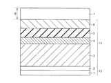
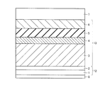
- FIG. 3 is a schematic cross-sectional view of the photoelectric conversion element of Embodiment 1.
- FIG. It is a typical expanded sectional view of an example of the unevenness
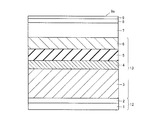
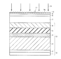
- 5 is a schematic cross-sectional view illustrating part of an example of the method for manufacturing the photoelectric conversion element according to Embodiment 1.
- FIG. FIG. 6 is a schematic cross-sectional view illustrating another part of the process of the example of the method for manufacturing the photoelectric conversion element according to the first embodiment.
- FIG. 6 is a schematic cross-sectional view illustrating another part of the process of the example of the method for manufacturing the photoelectric conversion element according to the first embodiment.
- FIG. 6 is a schematic cross-sectional view illustrating another part of the process of the example of the method for manufacturing the photoelectric conversion element according to the first embodiment.
- FIG. 6 is a schematic cross-sectional view illustrating another part of the process of the example of the method for manufacturing the photoelectric conversion element according to the first embodiment.
- FIG. 6 is a schematic cross-sectional view illustrating another part of the process of the example of the method for manufacturing the photoelectric conversion element according to the first embodiment.
- FIG. 6 is a schematic cross-sectional view illustrating another part of the process of the example of the method for manufacturing the photoelectric conversion element according to the first embodiment.
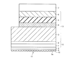
- FIG. 6 is a schematic cross-sectional view of a photoelectric conversion element according to Embodiment 2.
- FIG. FIG. 10 is a schematic cross-sectional view illustrating part of an example of the method for manufacturing the photoelectric conversion element according to the second embodiment.
- FIG. 10 is a schematic cross-sectional view illustrating another part of the process of the example of the method for manufacturing the photoelectric conversion element according to the second embodiment.
- FIG. 10 is a schematic cross-sectional view illustrating another part of the process of the example of the method for manufacturing the photoelectric conversion element according to the second embodiment.
- FIG. 1 shows a schematic cross-sectional view of the photoelectric conversion element of Embodiment 1 which is an example of the photoelectric conversion element of the present invention.
- the photoelectric conversion element of Embodiment 1 includes a template substrate 12, a semiconductor stacked body 13 provided on the template substrate 12, a transparent conductive layer 7 provided on the semiconductor stacked body 13, and a transparent conductive layer 7.
- a silicon oxide layer 8 provided, a silicon layer 9 provided on the silicon oxide layer 8, and a diffuse transmission layer 10 provided on the silicon layer 9 are provided.
- the diffuse transmission layer 10 is provided on the surface of the semiconductor laminate 13 opposite to the surface on the template substrate 12 installation side, and the diffusion transmission layer 10 side is the light receiving surface side.
- the template substrate 12 has a substrate 1 and a buffer layer 2 provided on the substrate 1.
- the semiconductor stacked body 13 includes an n-type nitride semiconductor layer 3 provided on the buffer layer 2, a nitride semiconductor buffer layer 4 provided on the n-type nitride semiconductor layer 3, and a nitride semiconductor buffer layer.
- 4 has an i-type nitride semiconductor layer 5 provided on 4 and a p-type nitride semiconductor layer 6 provided on i-type nitride semiconductor layer 5.
- the semiconductor stacked body 13 includes a pin structure including an n-type nitride semiconductor layer 3, an i-type nitride semiconductor layer 5, and a p-type nitride semiconductor layer 6.
- an n-pad electrode is formed on the surface of n-type nitride semiconductor layer 3 and a p-pad electrode is formed on the surface of p-type nitride semiconductor layer 6. Yes.
- the n pad electrode and the p pad electrode may not be installed, but are preferably installed.
- the surface 9a of the silicon layer 9 is a crystal plane with a ⁇ 100 ⁇ plane orientation, and preferably a (100) crystal plane.
- a diffuse transmission layer 10 is provided on the surface 9 a of the plane orientation (100) of the silicon layer 9. Further, unevenness 11 is provided on the surface of the diffuse transmission layer 10.
- the light incident on the diffuse transmission layer 10 is isotropically scattered by the unevenness 11 of the diffuse transmission layer 10.
- the diffuse transmittance of incident light ratio of diffuse transmitted light to incident light
- the optical path length of the light incident on the i-type nitride semiconductor layer 5 is increased.
- the amount of light absorbed by the i-type nitride semiconductor layer 5 is increased and a large number of photocarriers can be generated, so that characteristics such as short-circuit current density can be improved.
- the thickness t1 of the silicon layer 9 is preferably 0.03 ⁇ m or more and 0.05 ⁇ m or less.
- the thickness t1 of the silicon layer 9 is 0.03 ⁇ m or more, the characteristics of the silicon layer 9 as a bulk are enhanced, and the variation in the formation of the unevenness 11 of the diffuse transmission layer 10 tends to be reduced. is there.
- the thickness t1 of the silicon layer 9 is 0.05 ⁇ m or less, the amount of incident light transmitted through the silicon layer 9 tends to be suppressed by absorption of the silicon layer 9.
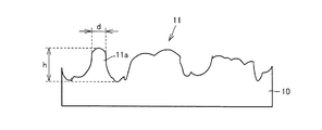
- FIG. 2 shows a schematic enlarged sectional view of an example of the irregularities 11 on the surface of the diffuse transmission layer 10.
- the material of the concavo-convex 11 of the diffuse transmission layer 10 is not particularly limited as long as it can scatter incident light isotropically. However, from the viewpoint of isotropically scattering light in a short wavelength region of 0.5 ⁇ m or less, the concavo-convex 11 The material is preferably a dielectric.
- the shape of the irregularities 11 of the diffuse transmission layer 10 is not particularly limited as long as the incident light can be isotropically scattered, but from the viewpoint of isotropically scattering light in a short wavelength region of 0.5 ⁇ m or less, It is preferable that the diameter d is 20 nm or more and 60 nm or less, and the height h is 1 nm or more and 50 nm or less.
- the convex and concave portions 11a having a diameter d of 20 nm or more and 60 nm or less and a height h of 1 nm or more and 50 nm or less, and the unevenness 11 made of a dielectric, is 0.5 ⁇ m or less, which is low in sensitivity in a conventional photoelectric conversion element.
- the incident light When light in the short wavelength region is incident, the incident light is isotropically scattered due to Rayleigh scattering, and the diffuse transmittance in the irregularities 11 tends to increase. As a result, the amount of incident light incident on the i-type nitride semiconductor layer 5 that is the photoelectric conversion layer increases, and more photocarriers can be generated in the i-type nitride semiconductor layer 5. There exists a tendency which can improve the characteristic of this photoelectric conversion element.
- the unevenness 11 on the surface of the diffuse transmission layer 10 is formed through a process of competition between etching and oxidation in ultrapure water from the surface of the silicon layer whose crystal orientation is (100).
- the protrusion 11a having a diameter d of 20 nm to 60 nm and a height h of 1 nm to 50 nm can be formed by etching in ultrapure water.
- corrugation 11 of the surface of the diffuse transmission layer 10 can be made into a silicon oxide by the oxidation in ultrapure water.
- the shape of the unevenness 11 on the surface of the diffusion transmission layer 10 of the photoelectric conversion element of the present embodiment has a shape having a convex portion 11a having a diameter d of 20 nm to 60 nm and a height h of 1 nm to 50 nm.
- the material of the irregularities 11 a dielectric by making the material of the irregularities 11 a dielectric, light in a short wavelength region of 0.5 ⁇ m or less can be effectively scattered isotropically to further improve the diffuse transmittance in the irregularities 11, and as a result, a short circuit. It exists in the tendency which can improve further the characteristics of photoelectric conversion elements, such as current density.
- the diameter d and the height h of the projections 11a of the projections and depressions 11 can be measured using, for example, an atomic force microscope (AFM).
- AFM atomic force microscope
- the height 11 is emphasized so that the convex portion 11a of the unevenness 11 is displayed in a granular shape.
- the unevenness 11 on the surface of the diffuse transmission layer 10 is formed through a competitive process between etching and oxidation in ultrapure water, the heightwise erosion of the unevenness 11 is further increased. Therefore, in the image of the unevenness 11 obtained by AFM, the height direction is further emphasized, and the convex portion 11a of the unevenness 11 is more easily displayed in a granular form.
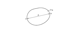
- the diameter d of the convex portion 11a is a line connecting any two points on the outer periphery of the planar shape when the convex portion 11a is viewed from a position vertically above the surface of the diffuse transmission layer 10. It shall mean the length of the line having the longest length among the minutes.
- the diameter d of the convex portion 11a can be calculated as follows, for example.
- FIG. 3 shows an example of a planar shape when the convex portion 11 a is viewed from a position vertically above the surface of the diffuse transmission layer 10.
- the planar shape of the convex portion 11a is generally formed by closing a straight line and / or a curved line, but in this example, the planar shape of the convex portion 11a is an ellipse. It has become a shape.
- two points (a point and b point) on the outer periphery of the planar shape of the convex part 11a are set so that the length of the line segment connecting the two arbitrary points on the outer periphery of the convex part 11a is the longest.
- the diameter d of the convex part 11a is computable by determining each, producing the line segment which makes each a point and b point both ends, and measuring the length of the line segment.
- the height h of the convex portion 11a means the maximum value of the height difference of each convex portion 11a as shown in FIG. That is, the height h of the convex portion 11a has a virtual horizontal plane (a plane parallel to the surface 9a of the silicon layer) including a point existing at the highest position in the vertical direction of the convex portion 11a in the vertical cross section of the concave and convex portion 11 and the convex portion 11a. It means a distance between a virtual horizontal plane (a plane parallel to the surface 9a of the silicon layer) including a point existing at the lowest position in the vertical direction of the portion 11a.
- the lowest position in the vertical direction of the convex portion 11a means a point that is present at a position closest to the surface 9a of the silicon layer in every vertical section along the vertical direction of the convex portion 11a.
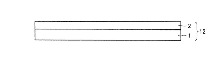
- a template substrate 12 is formed.
- the template substrate 12 is formed by laminating the buffer layer 2 for relaxing the lattice mismatch with the n-type nitride semiconductor layer 3 on the surface of the substrate 1 by, for example, the MOCVD (Metal Organic Chemical Vapor Deposition) method. Can be formed.
- the MOCVD Metal Organic Chemical Vapor Deposition
- the substrate 1 may be used.
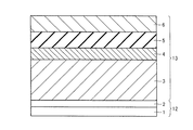
- n is formed on the surface of the buffer layer 2.
- Semiconductor laminate 13 having good crystallinity with few crystal defects by vapor-phase growth of type nitride semiconductor layer 3, nitride semiconductor buffer layer 4, i-type nitride semiconductor layer 5 and p-type nitride semiconductor layer 6 Tends to be formed.
- the substrate 1 Al x In y Ga z N (0 ⁇ x ⁇ 1,0 ⁇ y ⁇ 1,0 ⁇ z ⁇ 1, x + y + z ⁇ 0), GaP, GaAs, NdGaO 3, LiGaO 2, Al It is preferable to use a substrate having at least the surface of a material represented by the formula of 2 O 3 , MgAl 2 O 4 , ZnO, Si, SiC, SiGe, or ZrB 2 .
- buffer layer 2 for example, a nitride semiconductor represented by the formula of Al x0 In y0 Ga z0 N (0 ⁇ x0 ⁇ 1, 0 ⁇ y0 ⁇ 1, 0 ⁇ z0 ⁇ 1, x0 + y0 + z0 ⁇ 0), etc. Can be used.
- an n-type nitride semiconductor layer 3, a nitride semiconductor buffer layer 4, an i-type nitride semiconductor layer 5 and a p-type nitride semiconductor layer 6 are formed on the surface of the buffer layer 2, for example.
- the semiconductor stacked body 13 is formed by stacking by the MOCVD method or the like. Note that, after the semiconductor stacked body 13 is formed, the semiconductor stacked body 13 may be heated by performing an annealing process or the like of the semiconductor stacked body 13.
- the n-type nitride semiconductor layer 3 is, for example, a nitride semiconductor represented by the formula of Al x1 In y1 Ga z1 N (0 ⁇ x1 ⁇ 1, 0 ⁇ y1 ⁇ 1, 0 ⁇ z1 ⁇ 1, x1 + y1 + z1 ⁇ 0).
- a material doped with an n-type dopant can be used.
- silicon or the like can be used as the n-type dopant.
- N-type nitride semiconductor layer 3 can be stacked with a thickness of 0.1 ⁇ m or more and 4 ⁇ m or less, for example.
- the nitride semiconductor buffer layer 4 is made of, for example, a nitride semiconductor represented by the formula of Al x2 In y2 Ga z2 N (0 ⁇ x2 ⁇ 1, 0 ⁇ y2 ⁇ 1, 0 ⁇ z2 ⁇ 1, x2 + y2 + z2 ⁇ 0). And layers made of a nitride semiconductor represented by the formula of Al x3 In y3 Ga z3 N (0 ⁇ x3 ⁇ 1, 0 ⁇ y3 ⁇ 1, 0 ⁇ z3 ⁇ 1, x3 + y3 + z3 ⁇ 0) are alternately formed. A stacked structure can be used.
- the nitride semiconductor buffer layer 4 can be laminated with a thickness of, for example, about 0.08 ⁇ m.
- i-type nitride semiconductor layer 5 for example, a layer having an SQW (Single Quantum Well) structure or an MQW (Multiple Quantum Well) structure can be used.
- i-type nitride semiconductor layer 5 may have a single layer structure or a double hetero structure, for example.
- the i-type nitride semiconductor layer 5 having the MQW structure is represented by, for example, an expression of Al x4 In y4 Gaz4 N (0 ⁇ x4 ⁇ 1, 0 ⁇ y4 ⁇ 1, 0 ⁇ z4 ⁇ 1, x4 + y4 + z4 ⁇ 0).
- a layer in which barrier layers are alternately stacked can be used.
- the well layer and / or the barrier layer may be doped with an n-type dopant and / or a p-type dopant.
- the thickness of the well layer can be, for example, 1 nm or more and 20 nm or less, and the thickness of the barrier layer can be, for example, 1 nm or more and 10 nm or less.
- the p-type nitride semiconductor layer 6 for example, a nitride semiconductor represented by the formula of Al x6 In y6 Ga z6 N (0 ⁇ x6 ⁇ 1, 0 ⁇ y6 ⁇ 1, 0 ⁇ z6 ⁇ 1, x6 + y6 + z6 ⁇ 0).
- a material doped with a p-type dopant can be used.
- magnesium etc. can be used, for example.
- the thickness of the p-type nitride semiconductor layer 6 can be, for example, not less than 50 nm and not more than 2000 nm.
- a transparent conductive layer 7 is laminated on the surface of the p-type nitride semiconductor layer 6.
- the DC magnetron sputtering method is a method for sputtering a target by applying a voltage between a substrate and a target by a DC-continuous method.
- the DC-continuous method is a method in which a DC voltage having a predetermined magnitude (a voltage whose direction does not change with time) is continuously applied between a substrate and a target during sputtering of the target. It is.
- the method for forming the transparent conductive layer 7 using the DC magnetron sputtering method includes, for example, placing the wafer at the time when the semiconductor laminate 13 is formed on the template substrate 12 or the substrate 1 in a DC magnetron sputtering apparatus, A target is placed at a distance of, and a gas plasma is generated by applying a voltage by a DC-continuous method between the wafer and the target, the target is sputtered, the gas in the gas plasma, and the sputtered target To form a transparent conductive layer 7.
- the transparent conductive layer 7 for example, a conductive material can be used. When light is incident on the i-type nitride semiconductor layer 5 from the transparent conductive layer 7 side, incident light can be transmitted. Materials can be used.
- the transparent conductive layer 7 the single layer containing at least one metal selected from the group consisting of zinc (Zn), indium (In), tin (Sn), and magnesium (Mg), or the single layer It is preferable to use a plurality of layers in which a plurality of layers are stacked. In this case, the amount of light transmitted through the transparent conductive layer 7 tends to be increased.
- the plurality of layers may all be composed of a single layer of the same material, may be composed of a single layer of different materials, or may be composed of at least one single layer of different materials. Good.
- Examples of the single layer containing Zn include AZO in which ZnO is doped with Al, and GZO in which ZnO is doped with Ga.
- Examples of the single layer containing In and the single layer containing Sn include ITO (Indium Tin Oxide) which is a composite oxide of In and Sn.
- Examples of the single layer containing Mg include MgOH 2 doped with carbon (C).
- an AZO layer having a different Al concentration in the thickness direction may be formed using ZnO targets having different Al concentrations, and a GZO layer and an ITO layer are laminated. May be.
- the refractive index of the transparent conductive layer 7 is preferably larger than the refractive index of the diffuse transmission layer 10 and smaller than the refractive index of the p-type nitride semiconductor layer 6.
- optical loss such as reflection loss until the incident light incident from the diffuse transmission layer 10 side is transmitted and reaches the i-type nitride semiconductor layer 5 is reduced, and the i-type nitride semiconductor layer is reduced. 5 can increase the amount of photocarriers generated, the characteristics of the photoelectric conversion element such as the short-circuit current density tend to be improved.
- the refractive index of the diffusion transmission layer 10 is 1.5
- the refractive index of the p-type nitride semiconductor layer 6 is 2.3
- the refractive index of the transparent conductive layer 7 is preferably larger than 1.5 and smaller than 2.3.
- the thickness t2 of the transparent conductive layer 7 is preferably 0.25 ⁇ m or more and 0.5 ⁇ m or less.
- the transparent conductive layer 7 can form a good ohmic contact with the surface of the p-type nitride semiconductor layer 6, F.
- F the p-type nitride semiconductor layer 6
- the thickness t2 of the transparent conductive layer 7 is 0.25 ⁇ m or more and 0.5 ⁇ m or less
- the amount of light transmitted in a short wavelength region of 0.4 ⁇ m or more and 0.5 ⁇ m or less can be increased.
- the amount of photocarriers generated in i-type nitride semiconductor layer 5 can be increased.
- a silicon oxide layer 8 is laminated on the surface of the transparent conductive layer 7.
- the silicon oxide layer 8 As the base layer of the silicon layer 9, there is a tendency that the silicon layer 9 having a surface with good (100) plane orientation characteristics can be obtained.
- a method for laminating the silicon oxide layer 8 for example, at least one method selected from the group consisting of a vapor deposition method, a sputtering method, an ion plating method, and a chemical vapor deposition (CVD) method is used. it can.
- the thickness t3 of the silicon oxide layer 8 is preferably 0.03 ⁇ m or more and 0.15 ⁇ m or less.
- the silicon oxide layer 8 functions as a bulk, so that the silicon layer 9 having a surface with good (100) plane orientation characteristics can be obtained. The trend becomes larger.
- the thickness t3 of the silicon oxide layer 8 is 0.15 ⁇ m or less, the amount of light transmitted through the silicon oxide layer 8 can be increased, so that the amount of photocarriers generated in the i-type nitride semiconductor layer 5 can be reduced. Since it can increase, it exists in the tendency which can improve the characteristics of photoelectric conversion elements, such as a short circuit current density.
- a silicon layer 9 is laminated on the surface of the silicon oxide layer 8.
- the method for laminating the silicon layer 9 is not particularly limited, but it is preferable to use a DC magnetron sputtering method.
- the silicon layer 9 having a surface 9a having a (100) plane orientation very close to a single crystal tends to be obtained (Non-patent Document 1 ( Peter Reining et al., "Crystalline silicon films grown by pulsed dc magnetron sputtering", Journal of Non-Crystalline Solids 299-302 (2002), pp.128-132).
- silicon oxide is generally the main component in the region from the outermost surface of the silicon layer 9 to about 2 nm or less. Therefore, after the silicon oxide on the surface of the silicon layer 9 is removed by immersing the surface of the silicon layer 9 in hydrofluoric acid, the surface of the silicon layer 9 after the removal of the silicon oxide is rinsed with ultrapure water.
- the silicon layer 9 is immersed in the ultrapure water 21 accommodated in the container 22.
- the hydroxyl group (OH group) present in the ultrapure water 21 etches the surface of the silicon layer 9, and the dissolved oxygen in the ultrapure water 21 oxidizes the surface of the silicon layer 9, thereby causing the silicon layer 9.
- the diffuse transmission layer 10 is formed on the surface.
- the crystal plane of the crystal orientation (111) of the silicon crystal has an inclination of about 54 ° with respect to the crystal plane of the plane orientation (100), and is more resistant to etching than the crystal plane of the plane orientation (100). Since it is excellent, it is known that when a crystal plane with a plane orientation (100) of a silicon crystal is etched, a crystal plane with a plane orientation (111) remains. For this reason, when the surface of the silicon layer 9 with the surface orientation (100) is etched, a surface region with a surface orientation (111) that is less susceptible to etching tends to remain on the surface of the silicon layer 9.
- the oxidation rate due to dissolved oxygen is also different.
- the ultrapure water 21 has a specific resistance of 18 M ⁇ ⁇ cm to 100 M ⁇ ⁇ cm, an organic compound content of 1 ppb to 50 ppb, and a dissolved oxygen concentration of 1 ppb to 100 ppb. Is preferably used.
- This specification is ultrapure water used in a general IC (Integrated Circuit) production line, and higher quality ultrapure water may hinder the etching of the surface of the silicon layer 9 and the progress of oxidation. .
- the immersion of the surface of the silicon layer 9 in the ultrapure water 21 is preferably performed in a state where the ultrapure water 21 is held in the atmosphere. When used, oxygen in the atmosphere is mixed into the ultrapure water 21, so that the quality of the ultrapure water 21 is ultimately lowered.
- the temperature of the ultrapure water 21 is preferably 95 ° C. or higher and 100 ° C. or lower.
- the temperature of the ultrapure water 21 is 95 ° C. or more and 100 ° C. or less, the progress of etching and oxidation of the surface of the silicon layer 9 can be promoted.
- the unevenness 11) having the convex portion 11a having a height h of 1 nm to 50 nm and a height h of 20 nm to 60 nm can be formed with good reproducibility.
- the immersion time of the silicon layer 9 in the ultrapure water 21 is preferably 25 minutes or more and 35 minutes or less.
- the immersion time of the silicon layer 9 in the ultrapure water 21 is 25 minutes or more and 35 minutes or less, the progress of etching and oxidation of the surface of the silicon layer 9 can be promoted.
- the unevenness 11 (the unevenness 11 having the protrusion 11a having a diameter d of 20 nm to 60 nm and a height h of 1 nm to 50 nm) can be formed with good reproducibility.
- a gas 31 is sprayed on the surface of the diffuse transmission layer 10 having the irregularities 11. Thereby, the surface which has the unevenness
- air as the gas 31.
- air By using air as the gas 31, not only the cost of the gas is not required, but also the effect of promoting the natural oxidation of the surface of the irregularities 11 of the diffuse transmission layer 10 is manifested, which is preferable from the viewpoint of production technology.
- air is blown for 30 seconds or more at a pressure that removes moisture on the surface of the unevenness 11 of the diffuse transmission layer 10.
- moisture on the surface of the unevenness 11 of the diffuse transmission layer 10 can be removed, and the surface of the unevenness 11 of the diffusion transmission layer 10 tends to be sufficiently oxidized.
- the diffusion transmission layer 10, the silicon layer 9, the transparent conductive layer 7, and a part of the semiconductor laminate 13 are etched until the surfaces of the n-type nitride semiconductor layer 3 and the p-type nitride semiconductor layer 6 are exposed. To remove.
- an n pad electrode and a p pad electrode are formed on the exposed surface of n type nitride semiconductor layer 2 and the surface of p type nitride semiconductor layer 6, respectively, to manufacture the photoelectric conversion element of the first embodiment. it can.
- the semiconductor stacked body 13 includes one pin structure, but the semiconductor stacked body 13 may include two or more pin structures. In addition, other layers may be included between the above layers.
- n-type and p-type conductivity may be interchanged.
- the photoelectric conversion module may be formed by electrically connecting the p pad electrode of one photoelectric conversion element and the n pad electrode of another photoelectric conversion element.
- the photoelectric conversion module may be formed by electrically connecting the transparent conductive layer 7 of one photoelectric conversion element and the n-pad electrode of another photoelectric conversion element.
- FIG. 11 is a schematic cross-sectional view of the photoelectric conversion element of Embodiment 2, which is another example of the photoelectric conversion element of the present invention.
- a stacked body of the silicon oxide layer 8, the silicon layer 9, and the diffusion transmission layer 10 is provided on the surface on the installation side of the template substrate 12 among the surfaces of the semiconductor stacked body 13. The light is incident from the template substrate 12 side.
- the template substrate 12 is disposed between the diffuse transmission layer 10 and the semiconductor stacked body 13, and incident light incident on the diffusion transmission layer 10 is diffused and transmitted through the diffusion transmission layer 10. Isotropically scattered by the irregularities 11 on the surface of the silicon substrate 9, and then passes through the silicon layer 9, the silicon oxide layer 8, the template substrate 12, the n-type nitride semiconductor layer 3 and the nitride semiconductor buffer layer 4 to form the i-type nitride semiconductor layer 5. Incident light is generated in the i-type nitride semiconductor layer 5.
- the light incident on the diffuse transmission layer 10 is isotropically scattered by the unevenness 11 of the diffuse transmission layer 10.
- the diffuse transmittance of incident light on the irregularities 11 on the surface of the diffuse transmission layer 10 increases, so that more light is incident on the i-type nitride semiconductor layer 5, and the i-type nitride semiconductor layer 5.
- the optical path length of the light incident on is increased.
- the amount of light absorbed by the i-type nitride semiconductor layer 5 increases, and a large number of photocarriers can be generated. Therefore, characteristics of the photoelectric conversion element such as a short-circuit current density can be improved.
- n-type nitride semiconductor layer 3, nitride semiconductor buffer layer 4, i-type nitride semiconductor layer 5, p-type nitride semiconductor layer 6 and transparent conductive layer 7 are laminated on template substrate 12 in this order.
- the process is the same as in the first embodiment.
- a step of reducing the thickness of the substrate 1 is performed.
- the step of reducing the thickness of the substrate 1 can be performed by reducing the thickness of the substrate 1 by, for example, grinding and / or polishing the back surface of the substrate 1.
- a silicon oxide layer 8 is laminated on the back surface of the substrate 1, and then silicon is formed on the silicon oxide layer 8 as shown in the schematic cross-sectional view of FIG. Layer 9 is laminated.
- the silicon layer 9 is preferably formed using a DC magnetron sputtering method from the viewpoint of forming the surface 9a having a (100) plane orientation very close to a single crystal.
- the surface of the silicon layer 9 is immersed in hydrofluoric acid to remove the silicon oxide on the surface of the silicon layer 9, and then the surface of the silicon layer 9 after the removal of the silicon oxide is removed. Rinse with ultrapure water.
- the diffusive transmission layer 10 having the surface of the irregularities 11 is formed on the surface 9a of the plane orientation (100) of the silicon layer 9 by immersing the silicon layer 9 in ultrapure water. Thereafter, gas is blown onto the surface of the irregularities 11 of the diffuse transmission layer 10.
- the photoelectric conversion element of the second embodiment can be manufactured by forming an n pad electrode and a p pad electrode on the exposed surface of the n-type nitride semiconductor layer 3 and the surface of the transparent conductive layer 7, respectively.
- the transparent conductive layer 7 is provided on the surface of the p-type nitride semiconductor layer 6 .
- the p-type nitride semiconductor layer 6 has been transmitted.
- An opaque conductive layer such as a metal layer for reflecting transmitted light to the i-type nitride semiconductor layer 5 side may be provided.
- the characteristics of the photoelectric conversion element of Embodiment 2 such as the short circuit current density can be further improved.
- the case where the thickness of the substrate 1 of the template substrate 12 is reduced has been described. However, all of the template substrate 12 is removed and oxidized on the exposed back surface of the n-type nitride semiconductor layer 3.
- the silicon layer 8, the silicon layer 9, and the diffuse transmission layer 10 may be provided in this order. In this case, the incident light from the diffuse transmission layer 10 is not absorbed by the template substrate 12, and the amount of incident light on the i-type nitride semiconductor layer 5 can be increased. Therefore, when the amount of photocarriers generated in i-type nitride semiconductor layer 5 increases, characteristics of the photoelectric conversion element such as short-circuit current density can be further improved.
- a template substrate was prepared in which a buffer layer made of non-doped GaN was formed on the c-plane of a sapphire (Al 2 O 3 ) substrate.
- the template substrate was placed in the MOCVD apparatus, and the template substrate was heated to 1100 ° C. to 1120 ° C.
- trimethylgallium (TMG) gas is supplied into the MOCVD apparatus at a flow rate of 125 ( ⁇ mol / min), ammonia (NH 3 ) gas is supplied at a flow rate of 270 (mmol / min), and silane (
- TMG trimethylgallium
- NH 3 ammonia
- silane By supplying SiH 4 ) gas, an n-type nitride semiconductor layer made of an n-type GaN layer having a thickness of 1.5 ⁇ m was vapor-phase grown by MOCVD on the surface of the template substrate.
- the n-type nitride semiconductor layer was an n-type GaN layer doped with Si at a concentration of 2 ⁇ 10 18 / cm 3 .
- a well layer made of In 0.2 Ga 0.8 N having a thickness of 3.5 nm and a thickness of 6 nm are formed on the surface of the n-type nitride semiconductor layer.
- An i-type nitride semiconductor layer having an MQW structure in which six layers of GaN barrier layers were alternately stacked was vapor-grown by MOCVD.
- the well layer supplies TMG gas at a flow rate of 300 ( ⁇ mol / min) and trimethylindium (TMI) at a flow rate of 160 ( ⁇ mol / min) into the MOCVD apparatus, and further, NH 3 gas. was supplied at a flow rate of 425 (mmol / min).
- the barrier layer was formed only by stopping the supply of TMI gas into the MOCVD apparatus and supplying TMG gas and NH 3 gas.
- TMG gas is supplied at a flow rate of 125 ( ⁇ mol / min) into the MOCVD apparatus, and NH 3 gas is supplied at 270 (mmol / min).
- P-type nitride comprising a p-type GaN layer having a thickness of 50 nm on the surface of the i-type nitride semiconductor layer by further supplying biscyclopentadienylmagnesium (CP 2 Mg) gas.
- the semiconductor layer was vapor-phase grown by MOCVD.
- the p-type nitride semiconductor layer was a p-type GaN layer doped with Mg at a concentration of 4 ⁇ 10 19 / cm 3 .
- the wafer after the formation of the p-type nitride semiconductor layer was taken out of the MOCVD apparatus, and the wafer was annealed.
- the annealing process of the wafer was performed by holding the wafer at 800 ° C. for 5 minutes in a nitrogen atmosphere.
- the annealed wafer is placed in a DC magnetron sputtering apparatus, and a transparent conductive layer made of AZO having a thickness of 0.32 ⁇ m is formed on the surface of the p-type nitride semiconductor layer by DC magnetron sputtering.
- a single layer of AZO was formed as the transparent conductive layer.
- the partial pressure was changed from 3% to 10%, and the ZnO targets having different Al concentrations.
- Transparent conductive layers having different compositions such as an AZO layer formed from the above, a GZO layer formed from a ZnO target having Ga as a dopant instead of Al, or an ITO layer, may be formed.
- the wafer after the transparent conductive layer is formed is heated in a DC magnetron sputtering apparatus at 600 ° C. for 10 minutes to anneal the wafer. I did it.
- the atmosphere in the DC magnetron sputtering apparatus during the annealing treatment was maintained in a vacuum state with an oxygen partial pressure of 2%.
- the temperature of the wafer was lowered to 250 ° C., and the atmosphere pressure in the DC magnetron sputtering apparatus was set to a vacuum state (atmosphere pressure: 3 ⁇ 10 ⁇ 3 Pa) with an oxygen partial pressure of less than 1%. Then, using the SiO 2 target, a SiO 2 target at a deposition rate of 1.5 nm / sec, to form a silicon oxide layer of SiO 2 film having a thickness of 0.1 ⁇ m on the transparent conductive layer.
- the wafer temperature was raised to 400 ° C., and the atmosphere in the DC magnetron sputtering apparatus was replaced with an atmosphere having an Ar gas partial pressure of 100%.
- a Si target produced by a floating zone method is installed in a DC magnetron sputtering apparatus, and the Si target is pulsed at a frequency of 100 kHz, a duty ratio of 0.4, and an input energy density of 14.6 (nm ⁇ min) in an Ar gas atmosphere. ⁇ 1 ) / (W ⁇ cm ⁇ 2 ), a silicon layer having a surface with good (100) plane orientation characteristics is formed on the silicon oxide layer by a DC magnetron sputtering method to a thickness of 0.05 ⁇ m. Formed with.
- the surface of the silicon layer was left to stand in a class 1000 clean room for a whole day and night by naturally oxidizing the surface of the silicon layer to form a natural oxide film. Thereafter, the natural oxide film is removed by immersing the surface of the silicon layer in hydrofluoric acid having a hydrogen fluoride concentration of 2.5 mass% for 10 minutes, and the surface after removal of the natural oxide film is immediately treated with ultrapure water. Rinse.
- the surface of the silicon layer after rinsing is immersed in boiling ultrapure water for 30 minutes to form a diffuse transmission layer having an uneven surface on the surface (100) of the silicon layer. did.
- a wafer after forming a mask having an opening in a predetermined shape on the surface of the diffuse transmission layer is placed in an etching apparatus, and a part of the wafer is removed by etching from above the mask in the etching apparatus.
- a part of the surface of each of the n-type nitride semiconductor layer and the p-type nitride semiconductor layer was exposed.
- a mask having a shape in which an opening having a predetermined shape is located on each exposed surface of the n-type nitride semiconductor layer and the p-type nitride semiconductor layer is formed on the surface of the wafer after the etching. did.
- an Ni layer, a Pt layer, and an Au layer are stacked in this order from above the mask by a vapor deposition method to form a metal layer, and then the n-type nitride semiconductor layer and the p-type nitride semiconductor are removed by removing the mask.
- An n pad electrode and a p pad electrode were respectively formed on the exposed surface of the layer by lift-off.
- the wafer after the formation of the n-pad electrode and the p-pad electrode was placed in a lamp annealing apparatus, and the wafer was annealed by heating to 400 to 600 ° C.
- the sapphire substrate was peeled off. Then, the nitride semiconductor light-receiving element of Example 1 was obtained by dividing the wafer thus obtained at predetermined locations.
- the n pad electrode and the p pad electrode of the nitride semiconductor light receiving element of Example 1 are connected to the lead frame by gold wires, respectively, and the probe is brought into contact with the positive electrode and the negative electrode of the lead frame, respectively, for current and voltage measurement.
- the circuit was formed.
- the nitride semiconductor light-receiving element of Example 1 after the above circuit formation is installed in a solar simulator, and AM1.5 pseudo-sunlight is diffused and transmitted in an atmosphere of 25 mC at an energy density of 100 mW / cm 2.
- the IV curve of the nitride semiconductor light receiving element of Example 1 was obtained. From the IV curve, the open-circuit voltage (V oc ), short-circuit current density (J sc ), fill factor (FF), and photoelectric conversion efficiency (E ff ) of the nitride semiconductor light receiving device of Example 1 were calculated.
- the V oc of the nitride semiconductor light receiving device of Example 1 is 1.84 V
- J sc is 1.33 mA / cm 2
- F.I. F was 0.47
- E ff was 1.13%.
- Comparative Example 1 A nitride semiconductor light receiving device of Comparative Example 1 was fabricated in the same manner as in Example 1 except that the diffusion transmission layer was not formed.
- the V oc of the nitride semiconductor light receiving element of Comparative Example 1 is 1.82 V
- J sc is 0.89 mA / cm 2
- F.I. F was 0.47 and E ff was 0.76%.
- the nitride semiconductor light-receiving element of Example 1 was superior to the nitride semiconductor light-receiving element of Comparative Example 1 in terms of V oc , J sc, and E ff . This is because, in the nitride semiconductor light receiving element of Example 1, the incident light to the diffuse transmission layer is isotropically scattered by the unevenness of the surface of the diffuse transmission layer, so that more light is generated in the i-type nitride semiconductor layer. It can be considered that one of the major factors is that the light can be incident.
- a template substrate is formed by forming a buffer layer made of non-doped GaN on the c-plane of a sapphire substrate, and an n-type nitride semiconductor layer, an i-type nitride semiconductor layer, and a p-type nitride semiconductor are formed on the template substrate.
- the same steps as in Example 1 were performed until the layer and the transparent conductive layer were laminated in this order.
- the thickness of the sapphire substrate is reduced to 130 ⁇ m, and the ground surface of the sapphire substrate is polished Mirror finish was applied.
- the wafer after mirror finishing of the sapphire substrate is placed in a DC magnetron sputtering apparatus, and the atmospheric pressure in the DC magnetron sputtering apparatus is a vacuum state in which the oxygen partial pressure is less than 1% (atmospheric pressure: 3 ⁇ 10 ⁇ 3 Pa).
- the SiO 2 target, formed of SiO 2 target to 1.5 nm / sec. Speed of deposition, the sapphire substrate subjected to mirror polishing the silicon oxide layer of SiO 2 film having a thickness of 0.1 ⁇ m on the back surface did.
- the wafer temperature was raised to 400 ° C., and the atmosphere in the DC magnetron sputtering apparatus was replaced with an atmosphere having an Ar gas partial pressure of 100%.
- a Si target produced by a floating zone method is installed in a DC magnetron sputtering apparatus, and the Si target is pulsed at a frequency of 100 kHz, a duty ratio of 0.4, and an input energy density of 14.6 (nm ⁇ min) in an Ar gas atmosphere. ⁇ 1 ) / (W ⁇ cm ⁇ 2 ), a silicon layer having a surface with good (100) plane orientation characteristics is formed on the silicon oxide layer by a DC magnetron sputtering method to a thickness of 0.05 ⁇ m. Formed with.
- Example 2 Thereafter, in the same manner as in Example 1, a diffusion transmission layer having an uneven surface is formed on the surface of the silicon layer in the plane orientation (100), and air is blown on the uneven surface of the diffusion transmission layer for 30 seconds.
- the uneven surface of the diffuse transmission layer was dried, and at the same time, further natural oxidation of the diffuse transmission layer was promoted.
- the wafer after forming a mask having an opening in a predetermined shape on the surface of the diffuse transmission layer is placed in an etching apparatus, and in the etching apparatus, a part of the wafer is removed by etching from above the mask. A part of the surface of the n-type nitride semiconductor layer was exposed.
- a mask having a shape in which an opening having a predetermined shape is located on the surface of each of the n-type nitride semiconductor layer and the transparent conductive layer was formed on the surface of the wafer after the etching.
- the Ni layer, the Pt layer, and the Au layer are laminated by vapor deposition in this order from the upper side of the mask to form a metal layer, and then the surface of the n-type nitride semiconductor layer and the transparent conductive layer is removed by removing the mask.
- An n-pad electrode and a p-pad electrode were formed on each by lift-off.
- the wafer after the formation of the n-pad electrode and the p-pad electrode was placed in a lamp annealing apparatus, and the wafer was annealed by heating to 400 to 600 ° C.
- the nitride semiconductor light-receiving element of Example 2 was obtained by dividing the wafer obtained as described above at predetermined locations.
- Example 2 Thereafter, in the same manner as in Example 1, the V oc , J sc , F.V. F and E ff were calculated. As a result, the V oc of the nitride semiconductor light receiving element of Example 2 was 1.84 V, J sc was 0.87 mA / cm 2 , and F.I. F was 0.44 and E ff was 0.70%.
- Comparative Example 2 A nitride semiconductor light-receiving element of Comparative Example 2 was produced in the same manner as Example 2 except that the diffusion transmission layer was not formed.
- the V oc of the nitride semiconductor light receiving element of Comparative Example 2 is 1.83 V
- J sc is 0.76 mA / cm 2
- F.I. F was 0.44
- E ff was 0.61%.
- the nitride semiconductor light receiving device of Example 2 was superior to the nitride semiconductor light receiving device of Comparative Example 2 in terms of V oc , J sc, and E ff . This is because, in the nitride semiconductor light-receiving element of Example 2, the incident light to the diffuse transmission layer is isotropically scattered by the unevenness of the surface of the diffuse transmission layer, so that more light is emitted in the i-type nitride semiconductor layer. It can be considered that one of the major factors is that the light can be incident.
- the present invention can be used for a photoelectric conversion element and a method for manufacturing the photoelectric conversion element, and particularly for a solar cell using a nitride semiconductor and a method for manufacturing the solar cell.
Landscapes
- Photovoltaic Devices (AREA)
Abstract
半導体積層体(13)と、半導体積層体(13)上に設けられたシリコン層(9)と、シリコン層(9)上に設けられた拡散透過層(10)とを備え、シリコン層(9)は面方位{100}の表面を有し、拡散透過層(10)の表面が凹凸(11)を有する光電変換素子と光電変換素子の製造方法である。
Description
本発明は、光電変換素子および光電変換素子の製造方法に関する。
現在、光電変換素子は、シリコン(たとえば、非晶質シリコン、微結晶シリコンまたは多結晶シリコン)により作製されるのが一般的である。しかしながら、シリコンのバンドギャップは1.1eV~1.8eVであるため、エネルギの高い0.5μm以下の短波長領域の光に対しての感度が小さく、太陽光を有効活用できないという材料固有の課題を有していた。
これに対し、AlαInβGaγN(0≦α≦1、0≦β≦1、0≦γ≦1、α+β+γ≠0)の式で表わされる窒化物半導体のバンドギャップは、xおよびyの数値に対応して、0.7eV~6.0eVという極めて広い範囲で変化させることができる。そのため、窒化物半導体を用いて作製した光電変換素子は、0.5μm以下の短波長領域の光に対しても感度を持たせることができることから、次世代の光電変換素子として大変注目されている。
上記の窒化物半導体は、通常、有機金属気相成長法(MOCVD)、ハイドライド気相成長法(HVPE)、分子線気相成長法(MBE)、またはパルスレーザデポジション法(PLD)などの気相成長法を用いて基板上に形成することができる。
上記の窒化物半導体は、発光ダイオード(LED)およびレーザダイオード(LD)等の発光素子用の材料として好適であるため、開発が盛んに行なわれてきた経緯がある。また、近年では上記の窒化物半導体のバンドギャップの解明により、次世代の光電変換素子用の材料として、気相成長法を用いて窒化物半導体を形成する研究が盛んに行なわれている。
光電変換素子では、活性層が光を吸収してフォトキャリアを生成するため、活性層に多くの光を採り入れることが強く望まれる。たとえば、特許文献1(特開平7-288334号公報)、特許文献2(米国特許出願公開第2004/0118451号明細書)、および特許文献3(米国特許7217882号明細書)には、窒化物半導体を用いた光電変換素子の構造が開示されている。
Peter Reining et al., "Crystalline silicon films grown by pulsed dc magnetron sputtering", Journal of Non-Crystalline Solids 299-302 (2002), pp.128-132
Yuichi Sano et al, "Morphology change and its chemical states at the Si(100) surface after dipping in hot ultrapure water", Journal of Electron Spectroscopy and Related Phenomena 169 (2009), pp.92-96
しかしながら、特許文献1~3には、活性層に多くの光を採り入れることについての議論は存在しない。光電変換素子にとってフォトキャリアを多く生成することは短絡電流を増加させることを意味しているため、光電変換素子の特性を向上させる目的から、窒化物半導体を用いた光電変換素子の活性層でもフォトキャリアを多く生成することが要望されている。
上記の事情に鑑みて、本発明は、特性を向上させることができる光電変換素子および光電変換素子の製造方法を提供することを目的とする。
本発明は、半導体積層体と、半導体積層体上に設けられたシリコン層と、シリコン層上に設けられた拡散透過層とを備え、シリコン層は面方位{100}の表面を有し、拡散透過層の表面は凹凸を有する光電変換素子である。
ここで、本発明の光電変換素子においては、シリコン層の厚さが0.03μm以上0.05μm以下であることが好ましい。
また、本発明の光電変換素子において、凹凸は、径が20nm以上60nm以下であって、高さが1nm以上50nm以下の凸部を有することが好ましい。
また、本発明の光電変換素子において、基板をさらに備え、半導体積層体は基板上に設けられており、半導体積層体は、p型窒化物半導体層と、i型窒化物半導体層と、n型窒化物半導体層とを有することが好ましい。
また、本発明の光電変換素子において、基板は、AlxInyGazN(0≦x≦1、0≦y≦1、0≦z≦1、x+y+z≠0)、GaP、GaAs、NdGaO3、LiGaO2、Al2O3、MgAl2O4、ZnO、Si、SiC、SiGe、またはZrB2の式で表わされる材料を含むことが好ましい。
また、本発明の光電変換素子において、拡散透過層は、半導体積層体の表面のうち、基板の設置側の表面とは反対側の表面上に設けられていることが好ましい。
また、本発明の光電変換素子において、半導体積層体と拡散透過層との間に透明導電層をさらに備え、透明導電層は、亜鉛、インジウム、錫およびマグネシウムからなる群から選択された少なくとも1種の金属を含む単層、または単層の複数が積層された複数層を有し、透明導電層の屈折率は、拡散透過層の屈折率よりも大きく、かつp型窒化物半導体層の屈折率よりも小さくなっており、透明導電層の厚さは0.25μm以上0.5μm以下であることが好ましい。
また、本発明の光電変換素子において、拡散透過層は、半導体積層体の表面のうち、基板の設置側の表面上に設けられており、拡散透過層と半導体積層体との間に基板が配置されていることが好ましい。
さらに、本発明は、上記のいずれかの光電変換素子を製造する方法であって、半導体積層体を形成する工程と、半導体積層体上に面方位{100}の表面を有するシリコン層をDCマグネトロンスパッタ法により形成する工程と、を含む、光電変換素子の製造方法である。
ここで、本発明の光電変換素子の製造方法は、シリコン層をDCマグネトロンスパッタ法により形成する工程の後に、シリコン層を超純水に浸漬して拡散透過層を形成する工程をさらに含み、拡散透過層を形成する工程において、超純水は95℃以上100℃以下の温度で大気中に保持されており、シリコン層の超純水への浸漬時間は25分以上35分以下であることが好ましい。
また、本発明の光電変換素子の製造方法において、超純水の比抵抗は、18MΩ・cm以上100MΩ・cm以下であり、超純水中における有機化合物の含有量は、1ppb以上50ppb以下であって、超純水中における溶存酸素濃度は、1ppb以上100ppb以下であることが好ましい。
ここで、本発明の光電変換素子の製造方法において、拡散透過層の表面に空気を30秒以上吹き付ける工程をさらに含むことが好ましい。
また、本発明の光電変換素子の製造方法は、半導体積層体上に、蒸着法、スパッタ法、イオンプレーティング法および化学気相成長法からなる群から選択された少なくとも1つの方法により、厚さ0.03μm以上0.15μm以下の酸化シリコン層を形成する工程をさらに含み、シリコン層をDCマグネトロンスパッタ法により形成する工程は、酸化シリコン層上にシリコン層を形成する工程を含むことが好ましい。
本発明によれば、特性を向上することができる光電変換素子および光電変換素子の製造方法を提供することができる。
以下、本発明の実施の形態について説明する。なお、本発明の図面において、同一の参照符号は、同一部分または相当部分を表わすものとする。
<実施の形態1>
図1に、本発明の光電変換素子の一例である実施の形態1の光電変換素子の模式的な断面図を示す。実施の形態1の光電変換素子は、テンプレート基板12と、テンプレート基板12上に設けられた半導体積層体13と、半導体積層体13上に設けられた透明導電層7と、透明導電層7上に設けられた酸化シリコン層8と、酸化シリコン層8上に設けられたシリコン層9と、シリコン層9上に設けられた拡散透過層10と、を備えている。拡散透過層10は、半導体積層体13の表面のうち、テンプレート基板12の設置側の表面とは反対側の表面上に設けられており、拡散透過層10側が受光面側となっている。
図1に、本発明の光電変換素子の一例である実施の形態1の光電変換素子の模式的な断面図を示す。実施の形態1の光電変換素子は、テンプレート基板12と、テンプレート基板12上に設けられた半導体積層体13と、半導体積層体13上に設けられた透明導電層7と、透明導電層7上に設けられた酸化シリコン層8と、酸化シリコン層8上に設けられたシリコン層9と、シリコン層9上に設けられた拡散透過層10と、を備えている。拡散透過層10は、半導体積層体13の表面のうち、テンプレート基板12の設置側の表面とは反対側の表面上に設けられており、拡散透過層10側が受光面側となっている。
ここで、テンプレート基板12は、基板1と、基板1上に設けられたバッファ層2とを有している。
また、半導体積層体13は、バッファ層2上に設けられたn型窒化物半導体層3と、n型窒化物半導体層3上に設けられた窒化物半導体緩衝層4と、窒化物半導体緩衝層4上に設けられたi型窒化物半導体層5と、i型窒化物半導体層5上に設けられたp型窒化物半導体層6とを有している。なお、半導体積層体13は、n型窒化物半導体層3と、i型窒化物半導体層5と、p型窒化物半導体層6とから構成されているpin構造体を含んでいる。
なお、図示はしていないが、n型窒化物半導体層3の表面上にはnパッド電極が形成されているとともに、p型窒化物半導体層6の表面上にはpパッド電極が形成されている。nパッド電極およびpパッド電極はそれぞれ設置しなくてもよいが、設置しておくことが好ましい。
シリコン層9の表面9aは、面方位が{100}の結晶面であり、好ましくは(100)の結晶面である。シリコン層9の面方位(100)の表面9a上に拡散透過層10が設けられている。また、拡散透過層10の表面には凹凸11が設けられている。
実施の形態1の光電変換素子において、拡散透過層10に入射した光は、拡散透過層10の凹凸11で等方散乱する。これにより、拡散透過層10の表面の凹凸11における入射光の拡散透過率(入射光に対する拡散透過光の比率)が増大するため、より多くの光がi型窒化物半導体層5に入射することになり、i型窒化物半導体層5に入射した光の光路長が長くなることになる。これにより、i型窒化物半導体層5で吸収される光の量が増大し、フォトキャリアを多く生成することができることから、短絡電流密度等の特性を向上することができる。
ここで、シリコン層9の厚さt1は、0.03μm以上0.05μm以下であることが好ましい。シリコン層9の厚さt1が0.03μm以上である場合には、シリコン層9のバルクとしての特性が高くなって、拡散透過層10の凹凸11の形成のばらつきを低減することができる傾向にある。また、シリコン層9の厚さt1が0.05μm以下である場合には、シリコン層9の吸収によって、シリコン層9を透過する入射光量が低減するのを抑えることができる傾向にある。
図2に、拡散透過層10の表面の凹凸11の一例の模式的な拡大断面図を示す。拡散透過層10の凹凸11の材質は入射光を等方散乱させることができるものであれば特に限定されないが、0.5μm以下の短波長領域の光を等方散乱させる観点からは、凹凸11の材質は誘電体であることが好ましい。
また、拡散透過層10の凹凸11の形状も入射光を等方散乱させることができるものであれば特に限定されないが、0.5μm以下の短波長領域の光を等方散乱させる観点からは、径dが20nm以上60nm以下であって、高さhが1nm以上50nm以下の凸部11aを有する形状であることが好ましい。径dが20nm以上60nm以下であって、高さhが1nm以上50nm以下である凸部11aを有し、かつ誘電体からなる凹凸11に、従来の光電変換素子では感度の低い0.5μm以下の短波長領域の光が入射した場合には、レイリー散乱により入射光が等方散乱して、凹凸11における拡散透過率が増大する傾向にある。これにより、光電変換層であるi型窒化物半導体層5に入射する入射光量が増大して、i型窒化物半導体層5でより多くのフォトキャリアを生成することができるため、短絡電流密度等の光電変換素子の特性を向上することができる傾向にある。
たとえば後述するように、拡散透過層10の表面の凹凸11を、シリコン層の面方位が(100)の結晶面である表面から超純水中でエッチングと酸化との競合過程を経て形成した場合には、超純水中でエッチングにより、径dが20nm以上60nm以下であって高さhが1nm以上50nm以下である凸部11aを形成することができる。また、超純水中での酸化により拡散透過層10の表面の凹凸11の材質を酸化シリコンとすることができる。
したがって、本実施の形態の光電変換素子の拡散透過層10の表面の凹凸11の形状を径dが20nm以上60nm以下であって高さhが1nm以上50nm以下である凸部11aを有する形状とするとともに、凹凸11の材質を誘電体とすることによって、0.5μm以下の短波長領域の光を効果的に等方散乱させて凹凸11における拡散透過率をさらに向上させることができ、ひいては短絡電流密度等の光電変換素子の特性をさらに向上することができる傾向にある。
凹凸11の凸部11aの径dおよび高さhはそれぞれ、たとえば原子間力顕微鏡(AFM:Atomic Force Microscopy)を用いて測定することができる。AFMを用いた測定により得られる拡散透過層10の凹凸11の画像においては、高さ方向が強調されることによって、凹凸11の凸部11aが粒状に表示される。特に、拡散透過層10の表面の凹凸11が、超純水中でのエッチングと酸化との競合過程を経て形成されたものである場合には、凹凸11の高さ方向の浸食がさらに大きくなるため、AFMにより得られる凹凸11の画像においては、さらに高さ方向が強調されて、凹凸11の凸部11aがさらに粒状に表示されやすくなる。
なお、本明細書において、凸部11aの径dは、凸部11aを拡散透過層10の表面に対して垂直上方の位置から見たときの平面形状の外周上の任意の2点を結ぶ線分のうち長さが最長となる線分の長さを意味するものとする。
凸部11aの径dは、たとえば以下のようにして算出することができる。図3に、凸部11aを拡散透過層10の表面に対して垂直上方の位置から見たときの平面形状の一例を示す。たとえば図3に示すように、凸部11aの平面形状は、一般的に、直線および/または曲線が閉じられて形成されることになるが、本例においては、凸部11aの平面形状は楕円状となっている。そして、凸部11aの平面形状の外周上の任意の2点を結ぶ線分の長さが最長となるように、凸部11aの平面形状の外周上の2点(a点およびb点)をそれぞれ決定し、a点およびb点をそれぞれ両端とする線分を作成し、その線分の長さを測定することにより凸部11aの径dを算出することができる。
また、本明細書において、凸部11aの高さhは、たとえば図2に示すように、それぞれの凸部11aの高低差の最大値を意味するものとする。すなわち、凸部11aの高さhは、凹凸11の縦断面において、凸部11aの鉛直方向の最も高い位置に存在する点を含む仮想水平面(シリコン層の表面9aに平行な面)と、凸部11aの鉛直方向の最も低い位置に存在する点を含む仮想水平面(シリコン層の表面9aに平行な面)との間の距離を意味する。なお、凸部11aの鉛直方向の最も低い位置とは、凸部11aの鉛直方向に沿ったあらゆる縦断面のうち、シリコン層の表面9aに最も近い位置に存在する点を意味する。
以下、図4~図10の模式的断面図を参照して、実施の形態1の光電変換素子の製造方法の一例について説明する。
まず、図4に示すように、テンプレート基板12を形成する。テンプレート基板12は、たとえば、基板1の表面上に、n型窒化物半導体層3との格子不整合を緩和するためのバッファ層2をたとえばMOCVD(Metal Organic Chemical Vapor Deposition)法などによって積層することにより形成することができる。なお、テンプレート基板12に代えて、基板1のみを用いてもよいが、基板1の表面上にバッファ層2を形成したテンプレート基板12を用いた場合には、バッファ層2の表面上に、n型窒化物半導体層3、窒化物半導体緩衝層4、i型窒化物半導体層5およびp型窒化物半導体層6を気相成長させることによって結晶欠陥の少ない良好な結晶性を有する半導体積層体13を形成することができる傾向にある。
ここで、基板1としては、AlxInyGazN(0≦x≦1、0≦y≦1、0≦z≦1、x+y+z≠0)、GaP、GaAs、NdGaO3、LiGaO2、Al2O3、MgAl2O4、ZnO、Si、SiC、SiGe、またはZrB2の式で表わされる材料を少なくとも表面に有する基板を用いることが好ましい。
また、バッファ層2としては、たとえば、Alx0Iny0Gaz0N(0≦x0≦1、0≦y0≦1、0≦z0≦1、x0+y0+z0≠0)の式で表わされる窒化物半導体などを用いることができる。
次に、図5に示すように、バッファ層2の表面上に、n型窒化物半導体層3、窒化物半導体緩衝層4、i型窒化物半導体層5およびp型窒化物半導体層6をたとえばMOCVD法などによって積層することによって半導体積層体13を形成する。なお、半導体積層体13の形成後には、半導体積層体13のアニール処理などを行なうことによって、半導体積層体13を加熱してもよい。
n型窒化物半導体層3としては、たとえば、Alx1Iny1Gaz1N(0≦x1≦1、0≦y1≦1、0≦z1≦1、x1+y1+z1≠0)の式で表わされる窒化物半導体にn型ドーパントをドープさせたものなどを用いることができる。n型ドーパントとしては、たとえば、シリコンなどを用いることができる。n型窒化物半導体層3は、たとえば0.1μm以上4μm以下の厚さで積層することができる。
窒化物半導体緩衝層4としては、たとえば、Alx2Iny2Gaz2N(0≦x2≦1、0≦y2≦1、0≦z2≦1、x2+y2+z2≠0)の式で表わされる窒化物半導体からなる層と、Alx3Iny3Gaz3N(0≦x3≦1、0≦y3≦1、0≦z3≦1、x3+y3+z3≠0)の式で表わされる窒化物半導体からなる層と、が交互に積層されてなる構成を用いることができる。窒化物半導体緩衝層4は、たとえば0.08μm程度の厚さで積層することができる。
i型窒化物半導体層5としては、たとえば、SQW(Single Quantum Well)構造またはMQW(Multiple Quantum Well)構造を有するものを用いることができる。また、i型窒化物半導体層5は、たとえば、単層構造またはダブルヘテロ構造であってもよい。
MQW構造を有するi型窒化物半導体層5としては、たとえば、Alx4Iny4Gaz4N(0≦x4≦1、0≦y4≦1、0≦z4≦1、x4+y4+z4≠0)の式で表わされる窒化物半導体からなる井戸層と、Alx5Iny5Gaz5N(0≦x5≦1、0≦y5≦1、0≦z5≦1、x5+y5+z5≠0)の式で表わされる窒化物半導体からなる障壁層と、が交互に積層されてなるものを用いることができる。
なお、井戸層および/または障壁層には、n型ドーパントおよび/またはp型ドーパントがドープされていてもよい。また、井戸層の厚さはたとえば1nm以上20nm以下とすることができ、障壁層の厚さはたとえば1nm以上10nm以下とすることができる。
p型窒化物半導体層6としては、たとえば、Alx6Iny6Gaz6N(0≦x6≦1、0≦y6≦1、0≦z6≦1、x6+y6+z6≠0)の式で表わされる窒化物半導体にp型ドーパントをドープさせたものなどを用いることができる。なお、p型ドーパントとしては、たとえば、マグネシウムなどを用いることができる。p型窒化物半導体層6の厚さは、たとえば50nm以上2000nm以下とすることができる。
次に、図6に示すように、p型窒化物半導体層6の表面上に、透明導電層7を積層する。透明導電層7の積層方法としては、たとえば、DCマグネトロンスパッタ法を用いることができる。
なお、本明細書において、DCマグネトロンスパッタ法とは、基板とターゲットとの間にDC-continuous方式により電圧を印加することによってターゲットのスパッタリングを行なう方法である。また、本明細書において、DC-continuous方式とは、ターゲットのスパッタリング中に、所定の大きさの直流電圧(時間によって方向が変化しない電圧)を基板とターゲットとの間に連続的に印加する方式である。
DCマグネトロンスパッタ法を用いた透明導電層7の形成方法は、たとえば、DCマグネトロンスパッタ装置内にテンプレート基板12または基板1上に半導体積層体13を形成した時点のウエハを設置するとともに、ウエハと所定の距離を空けてターゲットを設置し、ウエハとターゲットとの間にDC-continuous方式により電圧を印加することによってガスプラズマを発生させ、ターゲットをスパッタリングして、ガスプラズマ中のガスと、スパッタリングしたターゲットとを反応させて透明導電層7を形成することにより行なうことができる。
透明導電層7としては、たとえば、導電性を有する材料を用いることができ、透明導電層7側からi型窒化物半導体層5に光を入射させる場合には、入射光を透過させることができる材料を用いることができる。なかでも、透明導電層7としては、亜鉛(Zn)、インジウム(In)、錫(Sn)およびマグネシウム(Mg)からなる群から選択された少なくとも1種の金属を含む単層、または当該単層の複数が積層された複数層を用いることが好ましい。この場合には、透明導電層7を透過する透過光量を増大することができる傾向にある。なお、複数層は、すべて同一材料の単層から構成されていてもよく、すべて互いに異なる材料の単層から構成されていてもよく、少なくとも1層が異なる材料の単層から構成されていてもよい。
また、Znを含む単層としては、たとえば、ZnOにAlがドープされたAZO、およびZnOにGaがドープされたGZOなどが挙げられる。また、Inを含む単層およびSnを含む単層としては、たとえば、InとSnの複合酸化物であるITO(Indium Tin Oxide)などが挙げられる。また、Mgを含む単層としては、たとえば、炭素(C)がドープされたMgOH2などが挙げられる。また、透明導電層7としては、たとえば、Al濃度が異なるZnOターゲットを用いて、厚さ方向にAl濃度の異なるAZO層を形成してもよく、GZO層とITO層などとを積層して形成してもよい。
透明導電層7の屈折率は、拡散透過層10の屈折率よりも大きく、かつp型窒化物半導体層6の屈折率よりも小さいことが好ましい。この場合には、拡散透過層10側から入射してきた入射光を透過してi型窒化物半導体層5に到達するまでの反射損失等の光学的損失を少なくして、i型窒化物半導体層5で発生するフォトキャリア量を多くすることができることから、短絡電流密度等の光電変換素子の特性を向上させることができる傾向にある。
たとえば、拡散透過層10が酸化シリコンからなる場合には、拡散透過層10の屈折率は1.5であり、p型窒化物半導体層6の屈折率は2.3であるため、この場合には、透明導電層7の屈折率を1.5よりも大きく、かつ2.3よりも小さくすることが好ましい。
透明導電層7の厚さt2は、0.25μm以上0.5μm以下であることが好ましい。透明導電層7の厚さt2が0.25μm以上0.5μm以下である場合には、透明導電層7がp型窒化物半導体層6の表面と良好なオーミック接触を形成することができるため、F.Fの低下を抑制して、光電変換素子の光電変換効率等の特性をより高くすることができる傾向にある。また、透明導電層7の厚さt2が0.25μm以上0.5μm以下である場合には、0.4μm以上0.5μm以下の短波長領域の光の透過量を高くすることができるため、i型窒化物半導体層5内で発生するフォトキャリア量を多くすることできる。これにより、i型窒化物半導体層5内で生成する短絡電流量を増大させることができるため、光電変換素子の短絡電流密度等の特性をより高くすることができる傾向にある。
次に、図7に示すように、透明導電層7の表面上に、酸化シリコン層8を積層する。シリコン層9の下地層として酸化シリコン層8を積層しておくことによって、良好な(100)の面方位特性の表面を有するシリコン層9が得られる傾向にある。
酸化シリコン層8の積層方法としては、たとえば、蒸着法、スパッタ法、イオンプレーティング法および化学気相成長(CVD:Chemical Vapor Deposition)法からなる群から選択された少なくとも1つの方法を用いることができる。
酸化シリコン層8の厚さt3は、0.03μm以上0.15μm以下であることが好ましい。酸化シリコン層8の厚さt3が0.03μm以上である場合には、酸化シリコン層8がバルクとして機能することにより、良好な(100)の面方位特性の表面を有するシリコン層9が得られる傾向が大きくなる。酸化シリコン層8の厚さt3が0.15μm以下である場合には、酸化シリコン層8を透過する透過光量を多くすることができるため、i型窒化物半導体層5で発生するフォトキャリア量を多くすることができることから、短絡電流密度等の光電変換素子の特性を向上させることができる傾向にある。
次に、図8に示すように、酸化シリコン層8の表面上に、シリコン層9を積層する。シリコン層9の積層方法は、特に限定されないが、DCマグネトロンスパッタ法を用いることが好ましい。DCマグネトロンスパッタ法を用いてシリコン層9を積層した場合には、極めて単結晶に近い(100)の面方位の表面9aを有するシリコン層9を得ることができる傾向にある(非特許文献1(Peter Reining et al., "Crystalline silicon films grown by pulsed dc magnetron sputtering", Journal of Non-Crystalline Solids 299-302 (2002), pp.128-132)参照)。
上記のシリコン層9の表面は大気中で酸化されて、一般的に、シリコン層9の最表面から2nm以下程度までの領域において酸化シリコンが主成分となっていることが知られている。そのため、シリコン層9の表面をフッ化水素酸に浸漬することによって、シリコン層9の表面の酸化シリコンを除去した後、酸化シリコンの除去後のシリコン層9の表面を超純水でリンスする。
そして、図9に示すように、容器22に収容された超純水21にシリコン層9を浸漬する。これにより、超純水21中に存在する水酸基(OH基)がシリコン層9の表面をエッチングするとともに、超純水21中の溶存酸素がシリコン層9の表面を酸化することによって、シリコン層9の表面に拡散透過層10が形成される。
一般に、シリコン結晶の面方位(111)の結晶面は、面方位(100)の結晶面に対して約54°の傾斜を有しており、面方位(100)の結晶面よりもエッチング耐性に優れているためにシリコン結晶の面方位(100)の結晶面をエッチングした場合には面方位(111)の結晶面が残ることが知られている。そのため、シリコン層9の面方位(100)の表面をエッチングした場合には、シリコン層9の表面にエッチングの影響を受けにくい面方位(111)の表面領域が残る傾向にある。
また、面方位(100)の表面領域と、面方位(111)の表面領域とでは、ダングリングボンドの密度が異なるために、溶存酸素による酸化速度も異なる。
このような超純水21によるシリコン層9の表面のエッチングと、超純水21中の溶存酸素によるシリコン層9の表面の酸化との競合過程を経て、シリコン層9の表面に凹凸11が形成されながらシリコン層9の表面が酸化して酸化シリコンとなって拡散透過層10が形成される(上記のエッチングと酸化とのメカニズムについては、非特許文献2(Yuichi Sano et al, "Morphology change and its chemical states at the Si(100) surface after dipping in hot ultrapure water", Journal of Electron Spectroscopy and Related Phenomena 169 (2009), pp.92-96)参照)。
なお、超純水21としては、比抵抗が18MΩ・cm以上100MΩ・cm以下であり、有機化合物の含有量が1ppb以上50ppb以下であって、溶存酸素濃度が1ppb以上100ppb以下である超純水が用いられることが好ましい。この仕様は、一般的なIC(Integrated Circuit)製造ラインで使用される超純水であり、これ以上の高品質の超純水はシリコン層9の表面のエッチングと酸化の進行を妨げるおそれがある。また、超純水21へのシリコン層9の表面の浸漬は、超純水21が大気中で保持された状態で行なわれることが好ましいが、上記の仕様以上の高品質の超純水21を用いた場合には大気中の酸素が超純水21中に混入することにより、最終的には超純水21の品質が下がることになる。さらに、大気中に製造ラインを設置することによって、超純水21中で拡散透過層10の凹凸11が形成された後に製造工程において大気に曝されることによって、さらなる酸化が進行することが好ましいため、大気中での用途に適する仕様は生産技術の面からも好ましい。
超純水21の温度は、95℃以上100℃以下であることが好ましい。超純水21の温度が95℃以上100℃以下である場合には、シリコン層9の表面のエッチングと酸化との進行を促進することができるため、上記の好ましい形状の凹凸11(径dが20nm以上60nm以下であって、高さhが1nm以上50nm以下である凸部11aを有する凹凸11)を再現性良く形成することができる傾向にある。
シリコン層9の超純水21への浸漬時間は25分以上35分以下であることが好ましい。シリコン層9の超純水21への浸漬時間が25分以上35分以下である場合には、シリコン層9の表面のエッチングと酸化との進行を促進することができるため、上記の好ましい形状の凹凸11(径dが20nm以上60nm以下であって、高さhが1nm以上50nm以下である凸部11aを有する凹凸11)を再現性良く形成することができる傾向にある。
次に、図10に示すように、拡散透過層10の凹凸11を有する表面にガス31を吹き付ける。これにより、拡散透過層10の凹凸11を有する表面を乾燥させることができる。
ここで、ガス31としては、空気を用いることが好ましい。ガス31に空気を用いることによって、ガスのコストを要しないだけでなく、拡散透過層10の凹凸11の表面の自然酸化を促す効果も発現するため、生産技術の面からも好ましい。
また、空気は、拡散透過層10の凹凸11の表面の水分を除去する程度の圧力で30秒以上吹き付けることが好ましい。この場合には、拡散透過層10の凹凸11の表面の水分を除去することができるとともに、拡散透過層10の凹凸11の表面を十分に酸化することができる傾向にある。
その後、n型窒化物半導体層3およびp型窒化物半導体層6の表面がそれぞれ露出するまで、拡散透過層10、シリコン層9、透明導電層7および半導体積層体13のそれぞれの一部をエッチングにより除去する。
その後、n型窒化物半導体層2の露出した表面およびp型窒化物半導体層6の表面にそれぞれnパッド電極およびpパッド電極を形成することによって実施の形態1の光電変換素子を製造することができる。
なお、上記においては、半導体積層体13がpin構造体を1つ含む場合について説明したが、半導体積層体13はpin構造体を2つ以上含んでいてもよい。また、上記の各層の間には他の層が含まれていてもよい。
また、上記においては、n型とp型の導電型を入れ替えてもよいことは言うまでもない。
さらに、1つの光電変換素子のpパッド電極と他の光電変換素子のnパッド電極とを電気的に接続して光電変換モジュールを形成してもよい。また、pパッド電極を形成しない場合には、1つの光電変換素子の透明導電層7と他の光電変換素子のnパッド電極とを電気的に接続して光電変換モジュールを形成してもよい。
<実施の形態2>
図11に、本発明の光電変換素子の他の一例である実施の形態2の光電変換素子の模式的な断面図を示す。実施の形態2の光電変換素子は、半導体積層体13の表面のうち、テンプレート基板12の設置側の表面上に、酸化シリコン層8、シリコン層9および拡散透過層10の積層体が設けられており、テンプレート基板12側から光を入射させることを特徴としている。
図11に、本発明の光電変換素子の他の一例である実施の形態2の光電変換素子の模式的な断面図を示す。実施の形態2の光電変換素子は、半導体積層体13の表面のうち、テンプレート基板12の設置側の表面上に、酸化シリコン層8、シリコン層9および拡散透過層10の積層体が設けられており、テンプレート基板12側から光を入射させることを特徴としている。
すなわち、実施の形態2の光電変換素子においては、拡散透過層10と半導体積層体13との間にテンプレート基板12が配置されており、拡散透過層10に入射した入射光は、拡散透過層10の表面の凹凸11で等方散乱した後に、シリコン層9、酸化シリコン層8、テンプレート基板12、n型窒化物半導体層3および窒化物半導体緩衝層4を通ってi型窒化物半導体層5に入射し、i型窒化物半導体層5内でフォトキャリアを発生させる。
実施の形態2の光電変換素子においても、拡散透過層10に入射した光は、拡散透過層10の凹凸11で等方散乱する。これにより、拡散透過層10の表面の凹凸11における入射光の拡散透過率が増大するため、より多くの光がi型窒化物半導体層5に入射することになり、i型窒化物半導体層5に入射した光の光路長が長くなることになる。これにより、i型窒化物半導体層5で吸収される光の量が増大し、フォトキャリアを多く生成することができることから、短絡電流密度等の光電変換素子の特性を向上することができる。
以下、実施の形態2の光電変換素子の製造方法の一例について説明する。まず、テンプレート基板12上に、n型窒化物半導体層3、窒化物半導体緩衝層4、i型窒化物半導体層5、p型窒化物半導体層6および透明導電層7をこの順に積層するまでの工程は実施の形態1と同様である。
次に、図12の模式的断面図に示すように、基板1の厚さを低減する工程を行なう。ここで、基板1の厚さを低減する工程は、たとえば、基板1の裏面を研削および/または研磨することなどによって基板1の厚さを低減することにより行なうことができる。
次に、図13の模式的断面図に示すように、基板1の裏面上に酸化シリコン層8を積層し、その後、図14の模式的断面図に示すように、酸化シリコン層8上にシリコン層9を積層する。なお、上述したように、シリコン層9は、極めて単結晶に近い(100)の面方位の表面9aを形成する観点から、DCマグネトロンスパッタ法を用いて形成することが好ましい。
その後、実施の形態1と同様にして、シリコン層9の表面をフッ化水素酸に浸漬してシリコン層9の表面の酸化シリコンを除去した後、酸化シリコンの除去後のシリコン層9の表面を超純水でリンスする。
次に、実施の形態1と同様にして、シリコン層9を超純水に浸漬することによってシリコン層9の面方位(100)の表面9a上に凹凸11の表面を有する拡散透過層10を形成し、その後、拡散透過層10の凹凸11の表面にガスを吹き付ける。
次に、透明導電層7、p型窒化物半導体層6、i型窒化物半導体層5および窒化物半導体緩衝層4のそれぞれの一部をエッチングにより除去することによって、n型窒化物半導体層3の表面を露出させる。
そして、n型窒化物半導体層3の露出した表面および透明導電層7の表面にそれぞれnパッド電極およびpパッド電極を形成することによって実施の形態2の光電変換素子を製造することができる。
実施の形態2においては、p型窒化物半導体層6の表面上に透明導電層7を設けた場合について説明したが、透明導電層7に代えて、p型窒化物半導体層6を透過してきた透過光をi型窒化物半導体層5側に反射するための金属層などの不透明な導電層を設けてもよい。この場合には、i型窒化物半導体層5で生成されるフォトキャリア量をさらに増大することができるため、短絡電流密度等の実施の形態2の光電変換素子の特性をさらに向上することができる。
また、実施の形態2においては、テンプレート基板12の基板1の厚さを低減する場合について説明したが、テンプレート基板12をすべて除去して、n型窒化物半導体層3の露出した裏面上に酸化シリコン層8、シリコン層9および拡散透過層10をこの順に設けてもよい。この場合には、拡散透過層10からの入射光がテンプレート基板12で吸収されず、i型窒化物半導体層5への入射光量を増大させることができる。そのため、i型窒化物半導体層5で発生するフォトキャリア量が増加することによって、短絡電流密度等の光電変換素子の特性をさらに向上することができる。
実施の形態2における上記以外の説明は、実施の形態1と同様であるため、その説明については省略する。
<実施例1>
まず、サファイア(Al2O3)基板のc面上にノンドープGaNからなるバッファ層が形成されたテンプレート基板を用意した。次に、MOCVD装置内にテンプレート基板を設置し、テンプレート基板を1100℃~1120℃まで加熱した。
まず、サファイア(Al2O3)基板のc面上にノンドープGaNからなるバッファ層が形成されたテンプレート基板を用意した。次に、MOCVD装置内にテンプレート基板を設置し、テンプレート基板を1100℃~1120℃まで加熱した。
次に、MOCVD装置内に、トリメチルガリウム(TMG)ガスを125(μmol/min)の流量で供給するとともに、アンモニア(NH3)ガスを270(mmol/min)の流量で供給し、さらにシラン(SiH4)ガスを供給することによって、テンプレート基板の表面上に、厚さ1.5μmのn型GaN層からなるn型窒化物半導体層をMOCVD法により気相成長させた。ここで、n型窒化物半導体層は、Siが2×1018個/cm3の濃度でドープされたn型GaN層であった。
次に、テンプレート基板の温度を750℃~800℃まで低下させた後、n型窒化物半導体層の表面上に、厚さ3.5nmのIn0.2Ga0.8Nからなる井戸層と、厚さ6nmのGaNからなる障壁層とを交互に6層ずつ積層したMQW構造を有するi型窒化物半導体層をMOCVD法により気相成長させた。ここで、井戸層は、MOCVD装置内に、TMGガスを300(μmol/min)の流量で供給するとともに、トリメチルインジウム(TMI)を160(μmol/min)の流量で供給し、さらにNH3ガスを425(mmol/min)の流量で供給することにより形成した。また、障壁層は、MOCVD装置内へのTMIガスの供給を停止し、TMGガスとNH3ガスとを供給することのみによって形成した。
次に、テンプレート基板の温度を1000℃~1030℃まで上昇させた後、MOCVD装置内に、TMGガスを125(μmol/min)の流量で供給するとともに、NH3ガスを270(mmol/min)の流量で供給し、さらにビスシクロペンタジエニルマグネシウム(CP2Mg)ガスを供給することによって、i型窒化物半導体層の表面上に、厚さ50nmのp型GaN層からなるp型窒化物半導体層をMOCVD法により気相成長させた。ここで、p型窒化物半導体層は、Mgが4×1019個/cm3の濃度でドープされたp型GaN層であった。
次に、p型窒化物半導体層の形成後のウエハをMOCVD装置内から取り出して、ウエハのアニール処理を行なった。ウエハのアニール処理は、窒素雰囲気中でウエハを800℃で5分間保持することにより行なった。
次に、上記のアニール処理後のウエハをDCマグネトロンスパッタ装置内に設置し、DCマグネトロンスパッタ法により、p型窒化物半導体層の表面上に厚さ0.32μmのAZOからなる透明導電層を形成した。ここで、AZOからなる透明導電層は、ターゲットとしてAl濃度が2%のZnOターゲットを用い、アルゴン(Ar)ガスと酸素(O2)ガスとの混合ガス雰囲気((O2ガス圧力/Arガス圧力)=3.8%)中で、ウエハの温度を180℃とした条件で、DCマグネトロンスパッタ法により形成した。
なお、本実施例においては、透明導電層としてAZOの単層を形成したが、導電率および透過率を向上させるために、分圧を3%~10%で変化させ、Al濃度が異なるZnOターゲットから形成したAZO層、Alに代えてドーパントをGaとしたZnOターゲットから形成したGZO層、またはITO層等の異なる組成の透明導電層を形成してもよい。
次に、AZOからなる透明導電層の結晶性および密着性を向上させるために、透明導電層の形成後のウエハをDCマグネトロンスパッタ装置内で600℃で10分間加熱することによってウエハのアニール処理を行なった。ここで、アニール処理時のDCマグネトロンスパッタ装置内の雰囲気を酸素分圧が2%の真空状態に保持した。
その後、ウエハの温度を250℃まで低下させ、DCマグネトロンスパッタ装置内の雰囲気の圧力を酸素分圧が1%未満の真空状態(雰囲気圧力:3×10⁻³Pa)とした。そして、SiO2ターゲットを用い、SiO2ターゲットから、1.5nm/secの堆積速度で、厚さ0.1μmのSiO2膜からなる酸化シリコン層を透明導電層上に形成した。
次に、ウエハの温度を400℃まで上昇させ、DCマグネトロンスパッタ装置内の雰囲気をArガス分圧が100%の雰囲気に置換した。そして、DCマグネトロンスパッタ装置内にフローティングゾーン法により作製されたSiターゲットを設置し、Arガス雰囲気中で、Siターゲットをパルス周波数100kHz、デューティー比0.4、投入エネルギ密度14.6(nm・min-1)/(W・cm-2)でスパッタすることによって、DCマグネトロンスパッタ法により、酸化シリコン層上に良好な(100)の面方位特性の表面を有するシリコン層を0.05μmの厚さで形成した。
次に、上記のシリコン層の形成後のウエハをクラス1000のクリーンルームに一昼夜放置することによって、シリコン層の表面を自然酸化して、自然酸化膜を形成した。その後、シリコン層の表面をフッ化水素濃度が2.5質量%のフッ化水素酸に10分間浸漬させることによって自然酸化膜を除去し、自然酸化膜の除去後の表面を直ちに超純水でリンスした。
次に、上記のリンス後のシリコン層の表面を沸騰している超純水に30分間浸漬させることによって、シリコン層の面方位(100)の表面上に凹凸の表面を有する拡散透過層を形成した。
次に、拡散透過層の凹凸の表面に空気を30秒間吹き付けることによって、拡散透過層の凹凸の表面を乾燥させると同時に、拡散透過層のさらなる自然酸化を促進した。
そして、拡散透過層の凹凸の表面をAFMで観察した結果、1辺が1μmの任意の正方形領域において、径が20nm以上60nm以下であって、高さが25nmまでの凸部を有する凹凸が確認された。
次に、拡散透過層の表面に所定形状に開口部が設けられたマスクを形成した後のウエハをエッチング装置内に設置し、エッチング装置においてマスクの上方からウエハの一部をエッチングにより除去することによって、n型窒化物半導体層およびp型窒化物半導体層のそれぞれの表面の一部を露出させた。
次に、上記のエッチング後のウエハの表面上に、n型窒化物半導体層およびp型窒化物半導体層のそれぞれの露出表面上に所定形状の開口部が位置するような形状を有するマスクを形成した。そして、マスクの上方から、Ni層、Pt層およびAu層をこの順に蒸着法によって積層して金属層を形成した後に、マスクを除去することによって、n型窒化物半導体層およびp型窒化物半導体層の露出表面上にそれぞれnパッド電極およびpパッド電極をリフトオフにより形成した。
次に、上記のnパッド電極およびpパッド電極の形成後のウエハをランプアニール装置内に設置し、ウエハを400~600℃に加熱することによって、ウエハのアニール処理を行なった。
次に、サファイア基板を研削して、研磨した後に、サファイア基板を剥離した。そして、このようにして得られたウエハを所定の箇所で分割することによって、実施例1の窒化物半導体受光素子を得た。
その後、実施例1の窒化物半導体受光素子のnパッド電極およびpパッド電極をそれぞれ金線によってリードフレームに接続し、リードフレームの正極と負極にそれぞれプローブを接触させることによって、電流および電圧測定用の回路を形成した。
そして、上記の回路形成後の実施例1の窒化物半導体受光素子をソーラシミュレータ内に設置し、AM1.5の擬似太陽光を100mW/cm2のエネルギ密度で25℃の雰囲気下で拡散透過層側から照射することによって、実施例1の窒化物半導体受光素子のI-V曲線を求めた。そのI-V曲線から実施例1の窒化物半導体受光素子の開放電圧(Voc)、短絡電流密度(Jsc)、曲線因子(F.F)および光電変換効率(Eff)を算出した。
その結果、実施例1の窒化物半導体受光素子のVocは1.84Vであり、Jscは1.33mA/cm2であり、F.Fは0.47であり、Effは1.13%であった。
<比較例1>
拡散透過層を形成しなかったこと以外は実施例1と同様にして比較例1の窒化物半導体受光素子を作製した。
拡散透過層を形成しなかったこと以外は実施例1と同様にして比較例1の窒化物半導体受光素子を作製した。
そして、実施例1と同様にして、比較例1の窒化物半導体受光素子のVoc、Jsc、F.FおよびEffを算出した。
その結果、比較例1の窒化物半導体受光素子のVocは1.82Vであり、Jscは0.89mA/cm2であり、F.Fは0.47であり、Effは0.76%であった。
<分析>
上記のとおり、実施例1の窒化物半導体受光素子は、比較例1の窒化物半導体受光素子と比べて、Voc、JscおよびEffの点で優れていた。これは、実施例1の窒化物半導体受光素子においては、拡散透過層の表面の凹凸によって、拡散透過層への入射光を等方散乱することによって、i型窒化物半導体層内により多くの光を入射することができたことが大きな要因の1つであると考えられる。
上記のとおり、実施例1の窒化物半導体受光素子は、比較例1の窒化物半導体受光素子と比べて、Voc、JscおよびEffの点で優れていた。これは、実施例1の窒化物半導体受光素子においては、拡散透過層の表面の凹凸によって、拡散透過層への入射光を等方散乱することによって、i型窒化物半導体層内により多くの光を入射することができたことが大きな要因の1つであると考えられる。
<実施例2>
まず、サファイア基板のc面上にノンドープGaNからなるバッファ層を形成することによってテンプレート基板を作製し、テンプレート基板上に、n型窒化物半導体層、i型窒化物半導体層、p型窒化物半導体層および透明導電層をこの順に積層するまでは実施例1と同様の工程を行なった。
まず、サファイア基板のc面上にノンドープGaNからなるバッファ層を形成することによってテンプレート基板を作製し、テンプレート基板上に、n型窒化物半導体層、i型窒化物半導体層、p型窒化物半導体層および透明導電層をこの順に積層するまでは実施例1と同様の工程を行なった。
次に、研削装置内にサファイア基板を設置して、1μm/secの割合でサファイア基板を研削することによって、サファイア基板の厚さを130μmまで低減し、サファイア基板の研削した面を研磨することによって鏡面加工を施した。
次に、サファイア基板の鏡面加工を施した後のウエハをDCマグネトロンスパッタ装置内に設置し、DCマグネトロンスパッタ装置内の雰囲気の圧力を酸素分圧が1%未満の真空状態(雰囲気圧力:3×10⁻³Pa)とした。そして、SiO2ターゲットを用い、SiO2ターゲットから、1.5nm/secの堆積速度で、厚さ0.1μmのSiO2膜からなる酸化シリコン層を鏡面加工を施したサファイア基板の裏面上に形成した。
次に、ウエハの温度を400℃まで上昇させ、DCマグネトロンスパッタ装置内の雰囲気をArガス分圧が100%の雰囲気に置換した。そして、DCマグネトロンスパッタ装置内にフローティングゾーン法により作製されたSiターゲットを設置し、Arガス雰囲気中で、Siターゲットをパルス周波数100kHz、デューティー比0.4、投入エネルギ密度14.6(nm・min-1)/(W・cm-2)でスパッタすることによって、DCマグネトロンスパッタ法により、酸化シリコン層上に良好な(100)の面方位特性の表面を有するシリコン層を0.05μmの厚さで形成した。
その後は、実施例1と同様にして、シリコン層の面方位(100)の表面に凹凸の表面を有する拡散透過層を形成し、拡散透過層の凹凸の表面に空気を30秒間吹き付けることによって、拡散透過層の凹凸の表面を乾燥させると同時に、拡散透過層のさらなる自然酸化を促進した。
そして、拡散透過層の凹凸の表面をAFMで観察した結果、1辺が1μmの任意の正方形領域において、径が20nm以上60nm以下であって、高さが25nmまでの凸部を有する凹凸が確認された。
その後、拡散透過層の表面に所定形状に開口部が設けられたマスクを形成した後のウエハをエッチング装置内に設置し、エッチング装置においてマスクの上方からウエハの一部をエッチングにより除去することによって、n型窒化物半導体層の表面の一部を露出させた。
次に、上記のエッチング後のウエハの表面上に、n型窒化物半導体層および透明導電層のそれぞれの表面上に所定形状の開口部が位置するような形状を有するマスクを形成した。そして、マスクの上方から、Ni層、Pt層およびAu層をこの順に蒸着法によって積層して金属層を形成した後に、マスクを除去することによって、n型窒化物半導体層および透明導電層の表面上にそれぞれnパッド電極およびpパッド電極をリフトオフにより形成した。
次に、上記のnパッド電極およびpパッド電極の形成後のウエハをランプアニール装置内に設置し、ウエハを400~600℃に加熱することによって、ウエハのアニール処理を行なった。
次に、上記のようにして得られたウエハを所定の箇所で分割することによって、実施例2の窒化物半導体受光素子を得た。
その後、実施例1と同様にして、実施例2の窒化物半導体受光素子のVoc、Jsc、F.FおよびEffを算出した。その結果、実施例2の窒化物半導体受光素子のVocは1.84Vであり、Jscは0.87mA/cm2であり、F.Fは0.44であり、Effは0.70%であった。
<比較例2>
拡散透過層を形成しなかったこと以外は実施例2と同様にして比較例2の窒化物半導体受光素子を作製した。
拡散透過層を形成しなかったこと以外は実施例2と同様にして比較例2の窒化物半導体受光素子を作製した。
そして、実施例2と同様にして、比較例2の窒化物半導体受光素子のVoc、Jsc、F.FおよびEffを算出した。
その結果、比較例2の窒化物半導体受光素子のVocは1.83Vであり、Jscは0.76mA/cm2であり、F.Fは0.44であり、Effは0.61%であった。
<分析>
上記のとおり、実施例2の窒化物半導体受光素子は、比較例2の窒化物半導体受光素子と比べて、Voc、JscおよびEffの点で優れていた。これは、実施例2の窒化物半導体受光素子においては、拡散透過層の表面の凹凸によって、拡散透過層への入射光を等方散乱することによって、i型窒化物半導体層内により多くの光を入射することができたことが大きな要因の1つであると考えられる。
上記のとおり、実施例2の窒化物半導体受光素子は、比較例2の窒化物半導体受光素子と比べて、Voc、JscおよびEffの点で優れていた。これは、実施例2の窒化物半導体受光素子においては、拡散透過層の表面の凹凸によって、拡散透過層への入射光を等方散乱することによって、i型窒化物半導体層内により多くの光を入射することができたことが大きな要因の1つであると考えられる。
今回開示された実施の形態および実施例はすべての点で例示であって制限的なものではないと考えられるべきである。本発明の範囲は上記した説明ではなくて請求の範囲によって示され、請求の範囲と均等の意味および範囲内でのすべての変更が含まれることが意図される。
本発明は、光電変換素子および光電変換素子の製造方法に利用することができ、特に窒化物半導体を用いた太陽電池およびその製造方法に利用することができる。
1 基板、2 バッファ層、3 n型窒化物半導体層、4 窒化物半導体緩衝層、5 i型窒化物半導体層、6 p型窒化物半導体層、7 透明導電層、8 酸化シリコン層、9 シリコン層、9a 表面、10 拡散透過層、11 凹凸、11a 凸部、12 テンプレート基板、13 半導体積層体、21 超純水、22 容器、31 ガス。
Claims (13)
- 半導体積層体(13)と、
前記半導体積層体(13)上に設けられたシリコン層(9)と、
前記シリコン層(9)上に設けられた拡散透過層(10)と、を備え、
前記シリコン層(9)は、面方位{100}の表面を有し、
前記拡散透過層(10)の表面は、凹凸(11)を有する、光電変換素子。 - 前記シリコン層(9)の厚さが0.03μm以上0.05μm以下である、請求項1に記載の光電変換素子。
- 前記凹凸(11)は、径が20nm以上60nm以下であって、高さが1nm以上50nm以下の凸部を有する、請求項1に記載の光電変換素子。
- 基板(1)をさらに備え、
前記半導体積層体(13)は前記基板(1)上に設けられており、
前記半導体積層体(13)は、p型窒化物半導体層(6)と、i型窒化物半導体層(5)と、n型窒化物半導体層(3)とを有する、請求項1に記載の光電変換素子。 - 前記基板(1)は、AlxInyGazN(0≦x≦1、0≦y≦1、0≦z≦1、x+y+z≠0)、GaP、GaAs、NdGaO3、LiGaO2、Al2O3、MgAl2O4、ZnO、Si、SiC、SiGe、またはZrB2の式で表わされる材料を含む、請求項4に記載の光電変換素子。
- 前記拡散透過層(10)は、前記半導体積層体(13)の表面のうち、前記基板(1)の設置側の表面とは反対側の表面上に設けられている、請求項4に記載の光電変換素子。
- 前記半導体積層体(13)と前記拡散透過層(10)との間に透明導電層(7)をさらに備え、
前記透明導電層(7)は、亜鉛、インジウム、錫およびマグネシウムからなる群から選択された少なくとも1種の金属を含む単層、または前記単層の複数が積層された複数層を有し、
前記透明導電層(7)の屈折率は、前記拡散透過層(10)の屈折率よりも大きく、かつ前記p型窒化物半導体層(6)の屈折率よりも小さくなっており、
前記透明導電層(7)の厚さは、0.25μm以上0.5μm以下である、請求項6に記載の光電変換素子。 - 前記拡散透過層(10)は、前記半導体積層体(13)の表面のうち、前記基板(1)の設置側の表面上に設けられており、
前記拡散透過層(10)と前記半導体積層体(13)との間に前記基板(1)が配置されている、請求項4に記載の光電変換素子。 - 請求項1に記載の光電変換素子を製造する方法であって、
前記半導体積層体(13)を形成する工程と、
前記半導体積層体(13)上に面方位{100}の表面を有するシリコン層(9)をDCマグネトロンスパッタ法により形成する工程と、を含む、光電変換素子の製造方法。 - 前記シリコン層(9)をDCマグネトロンスパッタ法により形成する工程の後に、前記シリコン層(9)を超純水(21)に浸漬して前記拡散透過層(10)を形成する工程をさらに含み、
前記拡散透過層(10)を形成する工程において、前記超純水(21)は95℃以上100℃以下の温度で大気中に保持されており、前記シリコン層(9)の前記超純水(21)への浸漬時間は25分以上35分以下である、請求項9に記載の光電変換素子の製造方法。 - 前記超純水(21)の比抵抗は、18MΩ・cm以上100MΩ・cm以下であり、
前記超純水(21)中における有機化合物の含有量は、1ppb以上50ppb以下であって、
前記超純水(21)中における溶存酸素濃度は、1ppb以上100ppb以下である、請求項10に記載の光電変換素子の製造方法。 - 前記拡散透過層(10)の前記表面に空気を30秒以上吹き付ける工程をさらに含む、請求項10に記載の光電変換素子の製造方法。
- 前記半導体積層体(13)上に、蒸着法、スパッタ法、イオンプレーティング法および化学気相成長法からなる群から選択された少なくとも1つの方法により、厚さ0.03μm以上0.15μm以下の酸化シリコン層(8)を形成する工程をさらに含み、
前記シリコン層(9)をDCマグネトロンスパッタ法により形成する工程は、前記酸化シリコン層(8)上に前記シリコン層(9)を形成する工程を含む、請求項9に記載の光電変換素子の製造方法。
Applications Claiming Priority (2)
| Application Number | Priority Date | Filing Date | Title |
|---|---|---|---|
| JP2011043876A JP2012182287A (ja) | 2011-03-01 | 2011-03-01 | 光電変換素子および光電変換素子の製造方法 |
| JP2011-043876 | 2011-03-01 |
Publications (1)
| Publication Number | Publication Date |
|---|---|
| WO2012117871A1 true WO2012117871A1 (ja) | 2012-09-07 |
Family
ID=46757810
Family Applications (1)
| Application Number | Title | Priority Date | Filing Date |
|---|---|---|---|
| PCT/JP2012/053822 Ceased WO2012117871A1 (ja) | 2011-03-01 | 2012-02-17 | 光電変換素子および光電変換素子の製造方法 |
Country Status (3)
| Country | Link |
|---|---|
| JP (1) | JP2012182287A (ja) |
| TW (1) | TW201242044A (ja) |
| WO (1) | WO2012117871A1 (ja) |
Cited By (1)
| Publication number | Priority date | Publication date | Assignee | Title |
|---|---|---|---|---|
| JP2015095648A (ja) * | 2013-11-08 | 2015-05-18 | 財團法人工業技術研究院Industrial Technology Research Institute | ヘテロ接合型太陽電池の構造 |
Families Citing this family (1)
| Publication number | Priority date | Publication date | Assignee | Title |
|---|---|---|---|---|
| JP6392501B2 (ja) | 2013-05-10 | 2018-09-19 | 新日鐵住金ステンレス株式会社 | 絶縁性に優れた熱膨張係数の小さいステンレス製太陽電池用基板およびその製造方法 |
Citations (4)
| Publication number | Priority date | Publication date | Assignee | Title |
|---|---|---|---|---|
| JPH07288334A (ja) * | 1994-04-18 | 1995-10-31 | Nichia Chem Ind Ltd | 窒化ガリウム系化合物半導体受光素子 |
| JPH1058236A (ja) * | 1996-08-12 | 1998-03-03 | Yuzo Mori | 超純水中の水酸基による加工方法 |
| JP2002299654A (ja) * | 2001-03-29 | 2002-10-11 | Toyota Motor Corp | 光起電力素子 |
| JP2008153570A (ja) * | 2006-12-20 | 2008-07-03 | Sharp Corp | 太陽電池の基体およびその製造方法、太陽電池モジュール |
-
2011
- 2011-03-01 JP JP2011043876A patent/JP2012182287A/ja active Pending
-
2012
- 2012-02-17 WO PCT/JP2012/053822 patent/WO2012117871A1/ja not_active Ceased
- 2012-02-24 TW TW101106270A patent/TW201242044A/zh unknown
Patent Citations (4)
| Publication number | Priority date | Publication date | Assignee | Title |
|---|---|---|---|---|
| JPH07288334A (ja) * | 1994-04-18 | 1995-10-31 | Nichia Chem Ind Ltd | 窒化ガリウム系化合物半導体受光素子 |
| JPH1058236A (ja) * | 1996-08-12 | 1998-03-03 | Yuzo Mori | 超純水中の水酸基による加工方法 |
| JP2002299654A (ja) * | 2001-03-29 | 2002-10-11 | Toyota Motor Corp | 光起電力素子 |
| JP2008153570A (ja) * | 2006-12-20 | 2008-07-03 | Sharp Corp | 太陽電池の基体およびその製造方法、太陽電池モジュール |
Non-Patent Citations (2)
| Title |
|---|
| P REINIG ET AL.: "Crystalline silicon films grown by pulsed dc magnetron sputtering", JOURNAL OF NON-CRYSTALLINE SOLIDS, vol. 299, no. 302, 2002, pages 128 - 132 * |
| Y SANO ET AL.: "Morphology change and its chemical states at the Si (1 0 0) surface after dipping in hot ultrapure water", JOURNAL OF ELECTRON SPECTROSCOPY AND RELATED PHENOMENA, vol. 169, 2009, pages 92 - 96 * |
Cited By (1)
| Publication number | Priority date | Publication date | Assignee | Title |
|---|---|---|---|---|
| JP2015095648A (ja) * | 2013-11-08 | 2015-05-18 | 財團法人工業技術研究院Industrial Technology Research Institute | ヘテロ接合型太陽電池の構造 |
Also Published As
| Publication number | Publication date |
|---|---|
| TW201242044A (en) | 2012-10-16 |
| JP2012182287A (ja) | 2012-09-20 |
Similar Documents
| Publication | Publication Date | Title |
|---|---|---|
| JP5608828B1 (ja) | 結晶シリコン太陽電池の製造方法、太陽電池モジュールの製造方法、結晶シリコン太陽電池並びに太陽電池モジュール | |
| US20100133529A1 (en) | Thin light-emitting devices and fabrication methods | |
| WO2008062685A1 (en) | Substrate provided with transparent conductive film for photoelectric conversion device, method for manufacturing the substrate, and photoelectric conversion device using the substrate | |
| WO2012020682A1 (ja) | 結晶シリコン系太陽電池 | |
| TWI811572B (zh) | 半導體發光元件及其製造方法 | |
| WO2012050186A1 (ja) | 結晶シリコン系太陽電池の製造方法 | |
| Duerinckx et al. | Reorganized porous silicon Bragg reflectors for thin-film silicon solar cells | |
| TWI722078B (zh) | 光電轉換裝置之製造方法 | |
| US9136422B1 (en) | Texturing a layer in an optoelectronic device for improved angle randomization of light | |
| Zhang et al. | Advanced radial junction thin film photovoltaics and detectors built on standing silicon nanowires | |
| JP5307688B2 (ja) | 結晶シリコン系太陽電池 | |
| JP2009290115A (ja) | シリコン系薄膜太陽電池 | |
| KR20090078275A (ko) | 요철 형태의 절연막을 포함하는 태양전지 및 그 제조방법 | |
| WO2012117871A1 (ja) | 光電変換素子および光電変換素子の製造方法 | |
| JP4756820B2 (ja) | 太陽電池 | |
| TWI476144B (zh) | 週期性奈米孔洞狀結構陣列之製造方法及其用途 | |
| TWI790245B (zh) | 光電轉換裝置之製造方法 | |
| Kim et al. | Progress in thin film free-standing monocrystalline silicon solar cells | |
| JP5090543B2 (ja) | 光電変換素子および光電変換素子の製造方法 | |
| JP5931653B2 (ja) | 光電変換素子 | |
| JP2011003639A (ja) | 結晶シリコン系太陽電池とその製造方法 | |
| JP2014187165A (ja) | 太陽電池の製造方法及び太陽電池製造装置 | |
| JP5858421B2 (ja) | 太陽電池の製造方法 | |
| JPWO2012073941A1 (ja) | 光電変換素子 | |
| JP5367780B2 (ja) | 光電変換素子 |
Legal Events
| Date | Code | Title | Description |
|---|---|---|---|
| 121 | Ep: the epo has been informed by wipo that ep was designated in this application |
Ref document number: 12752268 Country of ref document: EP Kind code of ref document: A1 |
|
| NENP | Non-entry into the national phase |
Ref country code: DE |
|
| 122 | Ep: pct application non-entry in european phase |
Ref document number: 12752268 Country of ref document: EP Kind code of ref document: A1 |