WO2012111379A1 - 半導体デバイスおよびその製造方法 - Google Patents
半導体デバイスおよびその製造方法 Download PDFInfo
- Publication number
- WO2012111379A1 WO2012111379A1 PCT/JP2012/051062 JP2012051062W WO2012111379A1 WO 2012111379 A1 WO2012111379 A1 WO 2012111379A1 JP 2012051062 W JP2012051062 W JP 2012051062W WO 2012111379 A1 WO2012111379 A1 WO 2012111379A1
- Authority
- WO
- WIPO (PCT)
- Prior art keywords
- layer
- group iii
- iii nitride
- nitride semiconductor
- substrate
- Prior art date
- Legal status (The legal status is an assumption and is not a legal conclusion. Google has not performed a legal analysis and makes no representation as to the accuracy of the status listed.)
- Ceased
Links
Images



Classifications
-
- H—ELECTRICITY
- H10—SEMICONDUCTOR DEVICES; ELECTRIC SOLID-STATE DEVICES NOT OTHERWISE PROVIDED FOR
- H10H—INORGANIC LIGHT-EMITTING SEMICONDUCTOR DEVICES HAVING POTENTIAL BARRIERS
- H10H20/00—Individual inorganic light-emitting semiconductor devices having potential barriers, e.g. light-emitting diodes [LED]
- H10H20/80—Constructional details
- H10H20/81—Bodies
- H10H20/822—Materials of the light-emitting regions
- H10H20/824—Materials of the light-emitting regions comprising only Group III-V materials, e.g. GaP
- H10H20/825—Materials of the light-emitting regions comprising only Group III-V materials, e.g. GaP containing nitrogen, e.g. GaN
-
- H—ELECTRICITY
- H10—SEMICONDUCTOR DEVICES; ELECTRIC SOLID-STATE DEVICES NOT OTHERWISE PROVIDED FOR
- H10H—INORGANIC LIGHT-EMITTING SEMICONDUCTOR DEVICES HAVING POTENTIAL BARRIERS
- H10H20/00—Individual inorganic light-emitting semiconductor devices having potential barriers, e.g. light-emitting diodes [LED]
- H10H20/01—Manufacture or treatment
- H10H20/011—Manufacture or treatment of bodies, e.g. forming semiconductor layers
- H10H20/013—Manufacture or treatment of bodies, e.g. forming semiconductor layers having light-emitting regions comprising only Group III-V materials
- H10H20/0133—Manufacture or treatment of bodies, e.g. forming semiconductor layers having light-emitting regions comprising only Group III-V materials with a substrate not being Group III-V materials
- H10H20/01335—Manufacture or treatment of bodies, e.g. forming semiconductor layers having light-emitting regions comprising only Group III-V materials with a substrate not being Group III-V materials the light-emitting regions comprising nitride materials
-
- H—ELECTRICITY
- H10—SEMICONDUCTOR DEVICES; ELECTRIC SOLID-STATE DEVICES NOT OTHERWISE PROVIDED FOR
- H10H—INORGANIC LIGHT-EMITTING SEMICONDUCTOR DEVICES HAVING POTENTIAL BARRIERS
- H10H20/00—Individual inorganic light-emitting semiconductor devices having potential barriers, e.g. light-emitting diodes [LED]
- H10H20/01—Manufacture or treatment
- H10H20/011—Manufacture or treatment of bodies, e.g. forming semiconductor layers
- H10H20/018—Bonding of wafers
-
- H—ELECTRICITY
- H10—SEMICONDUCTOR DEVICES; ELECTRIC SOLID-STATE DEVICES NOT OTHERWISE PROVIDED FOR
- H10H—INORGANIC LIGHT-EMITTING SEMICONDUCTOR DEVICES HAVING POTENTIAL BARRIERS
- H10H20/00—Individual inorganic light-emitting semiconductor devices having potential barriers, e.g. light-emitting diodes [LED]
- H10H20/80—Constructional details
- H10H20/81—Bodies
- H10H20/8215—Bodies characterised by crystalline imperfections, e.g. dislocations; characterised by the distribution of dopants, e.g. delta-doping
Definitions
- the present invention relates to a semiconductor device and a manufacturing method thereof, and more particularly to a vertical semiconductor device having high characteristics and a manufacturing method thereof.
- Vertical semiconductor devices are characterized by easy packaging and high area efficiency for both light-emitting devices and electronic devices.
- a method for manufacturing a vertical semiconductor device having such characteristics a method has been proposed in which a semiconductor layer grown on a base substrate is replaced with a support substrate different from the base substrate.
- Patent Document 1 discloses an uneven pattern on the surface of a semiconductor layer (the surface of an n-type semiconductor layer) after the base substrate is removed from a semiconductor layer grown on the base substrate. Disclosing to enhance light extraction of a semiconductor device by forming.
- Patent Document 2 discloses that an etching stop layer is interposed on an underlying substrate to grow a semiconductor layer, and the etching of the semiconductor layer after the underlying substrate is removed is performed on the etching stopping layer. It is disclosed that the contact characteristic of the n-side electrode is improved by reducing the damage of the semiconductor layer (n-type semiconductor layer) by stopping at n.
- Patent Document 3 discloses a method of performing laser lift-off of a support substrate by attaching a group III nitride semiconductor layer to a support substrate via a buffer layer and then etching away the buffer layer. Disclose ease.
- Each light-emitting device is a p-down type light-emitting device in which a p-type semiconductor layer of a semiconductor layer is bonded to a support substrate, and the base substrate is separated from the n-type semiconductor layer. The layer deteriorates and its surface becomes rough. Therefore, in the methods disclosed in Patent Document 1 to Patent Document 3 described above, it is difficult to bond the support substrate to the n-type semiconductor layer having a rough surface. Therefore, the n-type semiconductor layer is bonded to the support substrate. However, it is difficult to manufacture the n-down type semiconductor device.
- an n-type GaN layer is grown on the semiconductor layer because an etching stop layer having a unique property is interposed between the base substrate and the semiconductor layer.
- the crystallinity of the active layer and the p-type GaN layer is lowered, so that the characteristics of the semiconductor device are deteriorated.
- An object of the present invention is to solve the above problems and provide an n-down type semiconductor device having a semiconductor layer with high bonding property to a supporting substrate and high crystallinity.
- a semiconductor device includes a support substrate, a conductive layer disposed on the support substrate, and at least one group III nitride semiconductor layer disposed on the conductive layer, and includes a group III nitride semiconductor.
- the adjacent III-nitride semiconductor layer adjacent to the conductive layer has n-type conductivity, a dislocation density of 1 ⁇ 10 7 cm ⁇ 2 or less, and an oxygen concentration of 5 ⁇ 10 18 cm ⁇ . 3 or less.
- the oxygen concentration of the group III nitride semiconductor layer adjacent to the conductive layer can be 5 ⁇ 10 17 cm ⁇ 3 or less.
- the group III nitride semiconductor layer adjacent to the conductive layer may contain Al as a group III element constituting the group III nitride.
- a step of preparing a first composite substrate in which a first group III nitride semiconductor layer is bonded to a base substrate, and a first composite substrate A step of growing at least one second group III nitride semiconductor layer on the first group III nitride semiconductor layer, a temporary support substrate being bonded to the second group III nitride semiconductor layer, and a second step.
- Nitride semiconductor layer adjacent to conductive layer adjacent to conductive layer Group II nitride semiconductor layer has an n-type conductivity, dislocation density of 1 ⁇ 10 7 cm -2 or less, the oxygen concentration is 5 ⁇ 10 17 cm -3 or less.
- an n-down type semiconductor device having a semiconductor layer with high bonding property to a supporting substrate and high crystallinity.
- a semiconductor device 5 includes a support substrate 60, a conductive layer 50 disposed on the support substrate 60, and at least one layer disposed on the conductive layer 50.
- the group III nitride semiconductor layer 200 includes a group III nitride semiconductor layer 200, and the group III nitride semiconductor layer 200 c adjacent to the conductive layer 50 in the group III nitride semiconductor layer 200 has n-type conductivity and a dislocation density of 1 ⁇ 10 7 cm ⁇ 2 or less, and oxygen concentration is 5 ⁇ 10 18 cm ⁇ 3 or less.
- the semiconductor device 5 of this embodiment is an n-down type semiconductor device because the conductive layer adjacent group III nitride semiconductor layer 200c is n-type conductive, and has a dislocation density of 1 ⁇ 10 7 cm ⁇ 2 or less and Since the oxygen concentration is 5 ⁇ 10 18 cm ⁇ 3 or less, the crystallinity is high. Therefore, the group III nitride semiconductor layer 200 including the group III nitride semiconductor layer 200c adjacent to the conductive layer has high crystallinity, and the support substrate 60 Excellent bondability.
- the support substrate 60 in the semiconductor device 5 of the present embodiment is not particularly limited as long as it is suitable for supporting the group III nitride semiconductor layer 200 of the semiconductor device 5, but sapphire is used from the viewpoint of high light transmittance.
- a support substrate, a spinel support substrate, and the like are preferable.
- a Si support substrate, a group III nitride support substrate, and the like are preferable, and a thermal expansion coefficient that is the same as or close to that of the group III nitride semiconductor layer 200
- a group III nitride support substrate, a SiC support substrate, and the like are preferable.
- the support substrate 60 may be single crystal or polycrystal.
- a surface conductive layer 65 may be formed on the surface of the support substrate 60 from the viewpoint of increasing the bonding strength between the support substrate 60 and the conductive layer 50 described later.
- the chemical composition of the surface conductive layer 65 and the conductive layer 50 described later are the same or similar.
- the conductive layer 50 in the semiconductor device 5 of the present embodiment is not particularly limited as long as it can be an electrode of the semiconductor device 5, but from the viewpoint of reducing contact resistance, a metal layer such as an Al layer, a W layer, an Hf layer, When it is desired to have translucency, a conductive oxide layer such as an ITO (indium tin oxide) layer or a ZnO (zinc oxide) layer is preferable. Furthermore, a metal layer of Ti and / or Au may be included to improve adhesion and / or to form a pad electrode.
- Group III nitride semiconductor layer At least one group III nitride semiconductor layer 200 in the semiconductor device 5 of the present embodiment is formed so as to exhibit the function of the semiconductor device 5.
- the group III nitride semiconductor layer 200 can include, for example, an n + type semiconductor layer, an n ⁇ type semiconductor layer, and the like.
- the group III nitride semiconductor layer 200 can include, for example, a light emitting layer, an electron block layer, a contact layer, and the like.
- the group III nitride semiconductor layer 200c adjacent to the conductive layer 50 in the group III nitride semiconductor layer 200 has n-type conductivity and a dislocation density of 1 ⁇ 10 7 cm ⁇ 2 or less.
- the oxygen concentration is 5 ⁇ 10 18 cm ⁇ 3 or less.
- the semiconductor device 5 is an n-down type semiconductor device.
- the conductive layer adjacent group III nitride semiconductor layer 200c has high crystallinity such as a dislocation density of 1 ⁇ 10 7 cm ⁇ 2 or less and an oxygen concentration of 5 ⁇ 10 18 cm ⁇ 3 or less.
- the group III nitride semiconductor layer 200 including the oxide semiconductor layer 200c has high crystallinity.
- the conductive layer adjacent group III nitride semiconductor layer 200c has high flatness of the surface bonded to the conductive layer 50, the bonding property to the conductive layer 50 is good.
- the highly crystalline conductive layer adjacent group III nitride semiconductor layer 200c having a dislocation density of 1 ⁇ 10 7 cm ⁇ 2 or less and an oxygen concentration of 5 ⁇ 10 18 cm ⁇ 3 or less is used for forming the group III nitride It cannot be obtained by interposing a buffer layer on a base substrate whose chemical composition is not identical or approximate, and growing it on the base substrate. This is because when a buffer layer is formed on the base substrate and a group III nitride semiconductor layer is grown thereon, three-dimensional growth (non-planar growth, for example, a main surface and a facet is formed at the initial stage of the growth.
- the group III nitride semiconductor layer 200c adjacent to the conductive layer needs to be formed using a group III nitride semiconductor substrate having a density of 1 ⁇ 10 7 cm ⁇ 2 or less and an oxygen concentration of 5 ⁇ 10 18 cm ⁇ 3 or less.
- the oxygen concentration of the group III nitride semiconductor layer 200c adjacent to the conductive layer is 5 ⁇ 10 17 cm ⁇ . 3 or less is preferable.
- the conductive layer adjacent group III nitride semiconductor layer 200c having an oxygen concentration of 5 ⁇ 10 17 cm ⁇ 3 or less is directly grown on a base substrate having the same or similar chemical composition as the group III nitride forming the conductive layer. This is difficult, and can be suitably obtained by further growing on the group III nitride semiconductor layer grown on such a base substrate. Further, as the oxygen concentration of the group III nitride semiconductor layer is lower, the degree of two-dimensional growth (planar growth, for example, growth with the main surface as the crystal growth surface; the same applies hereinafter) rather than three-dimensional growth. For this reason, the crystallinity in the vicinity of joining with the conductive layer 50 and the flatness of the surface are increased, and uniform and good ohmic characteristics can be easily obtained in a plane parallel to the main surface.
- the group III nitride semiconductor layer 200c adjacent to the conductive layer preferably contains Al as a group III element constituting the group III nitride from the viewpoint of suppressing damage due to etching or the like during manufacturing. Damage can be reduced due to the fact that the Al—N bond is stronger than the Ga—N bond.
- the method for manufacturing semiconductor device 5 which is another embodiment of the present invention, includes a first composite in which first group III nitride semiconductor layer 210 is bonded to base substrate 10.
- the temporary support substrate 40 is bonded to the second group III nitride semiconductor layer 220, and the second composite substrate 2 (C in FIGS. 2 to 3 and 6), a step of removing the base substrate 10 from the second composite substrate 2 ((D) in FIGS. 2 to 3 and 6), a first III Conductive layer 50 is formed on group nitride semiconductor layer 210 2 (E in FIG. 2, (F) in FIGS. 3 and 6) and a step of bonding the support substrate 60 to the conductive layer 50 to form the third composite substrate 3 (FIG. 2F, FIG. 3 and 6 (G)) and a step of removing the temporary support substrate 40 from the third composite substrate 3 ((G) in FIG. 2, (H) in FIGS.
- the first group III nitride semiconductor layer 210 has n-type conductivity, a dislocation density of 1 ⁇ 10 7 cm ⁇ 2 or less, and an oxygen concentration of 5 ⁇ 10 18 cm ⁇ 3 or less. It is.
- the first group III nitride semiconductor layer 210 has n-type conductivity, a dislocation density of 1 ⁇ 10 7 cm ⁇ 2 or less, and an oxygen concentration of 5 ⁇ 10 18. Since it is equal to or less than cm ⁇ 3 , at least one second group III nitride semiconductor layer 220 having high crystallinity can be grown on the first group III nitride semiconductor layer 210 and the first group III nitride semiconductor layer 210 can be grown.
- the planarity of the surface of the first group III nitride semiconductor layer 210 after removing the base substrate 10 from the group nitride semiconductor layer 210 is increased, and the first group III nitride semiconductor layer 210 and the conductive layer 50 are joined. Sexuality can be increased.
- Step of preparing the first composite substrate Referring to (A) in FIGS. 2 to 3 and 6, the step of preparing first composite substrates 1 A and 1 B is not particularly limited, but base substrate 10 and first group III nitride semiconductor layer 210 are not limited. 7 and 8 are preferably included from the viewpoint of improving the bonding property with each other and facilitating the separation of the two.
- the process of preparing the first composite substrate 1A will be described below.
- the base substrate 10 is not particularly limited, but the first group III nitride is used when the second group III nitride semiconductor layer 220 is grown on the first group III nitride semiconductor layer 210 in a later step.
- the base substrate 10 is peeled off by laser lift-off, the base substrate 10 is used so that the laser passes through the base substrate 10 and is absorbed by the first group III nitride semiconductor layer 210.
- the base substrate 10 is peeled off by laser lift-off, the base substrate 10 is used so that the laser passes through the base substrate 10 and is absorbed by the first group III nitride semiconductor layer 210.
- the method for forming the SiO 2 layers 12a and 12b is not particularly limited, and a plasma CVD (chemical vapor deposition) method, a sputtering method, a vacuum evaporation method, and the like are preferable.
- a sub-process of bonding the SiO 2 layer 12a formed on the base substrate 10 and the SiO 2 layer 12b formed on the group III nitride semiconductor substrate 20 is included.
- the two SiO 2 layers 12 a and 12 b are integrated into the SiO 2 layer 12.
- the method of bonding is not particularly limited, and the surfaces of the surfaces to be bonded are cleaned and bonded directly, and then the temperature is raised to 700 ° C. to 1000 ° C. for bonding, and a metal film is formed and contacted.
- An alloy bonding method in which the metal of the metal film is alloyed by raising the temperature while being heated, and a surface activation method in which the bonding surface is activated and bonded by plasma or ions are preferably used.
- first composite substrate 1B With reference to FIG. 8, the process of preparing the 1st composite substrate 1B is demonstrated below.
- FIG. 8A a sub-process for sequentially forming first SiO 2 layer 14, amorphous Si layer 16 and second SiO 2 layer 18a on base substrate 10, and a group III nitride semiconductor Forming a second SiO 2 layer 18b on one main surface of the substrate 20 and then implanting ions from the main surface into the surface P having a certain depth to embrittle the region of the surface P; including.
- the base substrate 10 is not particularly limited, but the first group III nitride is used when the second group III nitride semiconductor layer 220 is grown on the first group III nitride semiconductor layer 210 in a later step. From the viewpoint of preventing cracks from occurring in the semiconductor layer 210, it is preferable to use a group III nitride base substrate having the same or similar chemical composition as the first group III nitride semiconductor layer 210.
- the method for forming the first SiO 2 layer 14, the amorphous Si layer 16, and the second SiO 2 layers 18a and 18b is not particularly limited, and a plasma CVD (chemical vapor deposition) method, a sputtering method, or a vacuum evaporation method is used. The method etc. are mentioned suitably.
- the two second SiO 2 layers 18 a and 18 b are integrated into the second SiO 2 layer 18.
- the method of bonding is not particularly limited, and the surfaces of the surfaces to be bonded are cleaned and bonded directly, and then the temperature is raised to 700 ° C. to 1000 ° C. for bonding, and a metal film is formed and contacted.
- An alloy bonding method in which the metal of the metal film is alloyed by raising the temperature while being heated, and a surface activation method in which the bonding surface is activated and bonded by plasma or ions are preferably used.
- base substrate 10 and group III nitride semiconductor are interposed with first SiO 2 layer 14, amorphous Si layer 16 and second SiO 2 layer 18 interposed therebetween.
- first SiO 2 layer 14 amorphous Si layer 16 and second SiO 2 layer 18 interposed therebetween.
- first group III nitride semiconductor layer 210 and the remaining portion of the group III nitride semiconductor substrate 20 are left on the surface P embrittled by ion implantation.
- the first group III nitride semiconductor substrate 21 is separated from the first group III nitride semiconductor substrate 21 with the first SiO 2 layer 14, the amorphous Si layer 16 and the second SiO 2 layer 18 interposed on the base substrate 10.
- a first composite substrate 1B to which the physical semiconductor layer 210 is bonded is obtained.
- the first group III nitride semiconductor layer 210 in the first composite substrates 1A and 1B has n-type conductivity, a dislocation density of 1 ⁇ 10 7 cm ⁇ 2 or less, and an oxygen concentration of 5 ⁇ 10 18 cm -3 or less Since the first group III nitride semiconductor layer 210 has n-type conductivity, it is easy to manufacture an n-down type semiconductor device in which the n-type semiconductor layer is bonded to the support substrate. Since the first group III nitride semiconductor layer 210 has a dislocation density of 1 ⁇ 10 7 cm ⁇ 2 or less and an oxygen concentration of 5 ⁇ 10 18 cm ⁇ 3 or less, it has at least high crystallinity thereon.
- One second group III-nitride semiconductor layer 220 can be grown.
- the first group III nitride semiconductor layer 210 with high crystallinity having a dislocation density of 1 ⁇ 10 7 cm ⁇ 2 or less and an oxygen concentration of 5 ⁇ 10 18 cm ⁇ 3 or less is used for forming the group III nitride forming the same. It cannot be obtained by a method in which a buffer layer is interposed on a base substrate whose chemical composition is not the same or approximate, and the buffer layer is grown thereon. This is because when a buffer layer is formed on the base substrate and a group III nitride semiconductor layer is grown thereon, three-dimensional growth occurs at the initial stage of growth, so that the group III nitride semiconductor layer to be grown is grown.
- the group III nitride crystal semiconductor layer becomes more dominant from three-dimensional growth to two-dimensional growth as the growth proceeds, so that the dislocation density and the oxygen concentration decrease in the middle and later stages of the growth. Therefore, dislocation density cut out from a group III nitride semiconductor ingot grown using another base substrate (for example, a base substrate having the same or similar chemical composition as the group III nitride to be formed, although there is no particular limitation).
- the growth method includes at least 1 layer on the first group III nitride semiconductor layer 210.
- the method is not particularly limited as long as the second group III nitride semiconductor layer 220 can be epitaxially grown.
- the MOVPE (organic metal vapor phase epitaxy) method, the HVPE (hydride vapor phase epitaxy) method, the MBE (molecular beam) Preferred examples include a gas phase method such as a growth method and a sublimation method, a liquid phase method such as a flux method, and a high nitrogen pressure solution method.
- the second group III nitride semiconductor layer 220 obtained in the growth process of the second group III nitride semiconductor layer 220 has a dislocation density of 1 ⁇ 10 7 cm ⁇ 2 or less and an oxygen concentration of 5 ⁇ 10 18 cm ⁇ 3. Since it is epitaxially grown on the following first group III nitride semiconductor layer 210 with high crystallinity, it has high crystallinity.
- Electrode formation process After the growth step of the second group III nitride semiconductor layer 220, a step of forming the electrode 30 on the outermost layer of the second group III nitride semiconductor layer 220 (electrode formation step) can be included.
- the method of bonding the second group III nitride semiconductor layer 220 and the temporary support substrate 40 in the step of forming the second composite substrate 220 is as follows.
- the group III nitride semiconductor layer 220 can be sufficiently supported by the temporary support substrate 40 and can be easily removed from the second group III nitride semiconductor layer 220 in a later step.
- the second group III nitride semiconductor layer 220 and the temporary support substrate 40 are used. Can be securely bonded together.
- the temporary support substrate 40 is not particularly limited as long as it can sufficiently support the second group III nitride semiconductor layer 220.
- the sapphire temporary support substrate, the Si temporary support substrate, and the group III nitride are not limited.
- a semiconductor temporary support substrate and the like are preferable.
- the second composite substrate 2 is obtained by bonding the temporary support substrate 40 to the second group III nitride semiconductor layer 220.
- the method of removing the base substrate 10 from the second composite substrate 2 in the base substrate 10 removal step is not particularly limited, but the efficiency From the standpoint of removal, a laser lift-off method is preferable.
- the laser lift method refers to a method of separating a part of a composite substrate by irradiating the composite substrate with a laser beam and decomposing a part of a part of layers constituting the composite substrate.
- the type of laser light used for laser lift-off, the separation position, and the separation mechanism are different. This will be described in more detail below.
- the second composite substrate 2 including the first composite substrate 1A includes a base substrate 10, a SiO 2 layer 12, a first group III nitride semiconductor layer 210, and a second III.
- Group nitride semiconductor layer 220 has a stacked structure in this order. Such a structure is such that the base substrate 10 does not absorb light having a wavelength that the first and second group III nitride semiconductor layers 210 and 220 absorb, such as a sapphire base substrate, a spinel base substrate, a gallium oxide base substrate, and the like. It is suitably adopted when it is.
- the lift-off of the base substrate 10 is as follows. To be done. From the base substrate 10 side of the second composite substrate 2, light having a wavelength that is not absorbed by the base substrate 10 and the SiO 2 layer 12 but is absorbed by the first group III nitride semiconductor layer 210, for example, having a wavelength of 355 nm THG (third harmonic) -YAG (yttrium, aluminum, garnet) laser light is irradiated. Part of the first group III nitride semiconductor layer 210 that has absorbed the THG-YAG laser light is decomposed, and the base substrate 10 and the SiO 2 layer 12 are lifted off from the first group III nitride semiconductor layer 210.
- THG third harmonic
- YAG yttrium, aluminum, garnet
- the second composite substrate 2 including the first composite substrate 1B includes a base substrate 10, a first SiO 2 layer 14, an amorphous Si layer 16, a second SiO 2
- the two layers 18, the first group III nitride semiconductor layer 210, and the second group III nitride semiconductor layer 220 are stacked in this order.
- the base substrate 10 is a substrate that absorbs light having a wavelength that is absorbed by the first and second group III nitride semiconductor layers 210 and 220, such as a group III nitride base substrate. Adopted.
- the base substrate The lift-off of 10 is performed as follows. From the base substrate 10 side of the second composite substrate 2, light of a wavelength that is not absorbed by the base substrate 10 and the first and second SiO 2 layers 14, 18 but is absorbed by the amorphous Si layer 16, for example, wavelength Irradiation with 532 nm SHG (second harmonic) -YAG (yttrium, aluminum, garnet) laser light is performed.
- the SHG-YAG laser light is absorbed by the amorphous Si layer 16 and converted into heat, and a part of the base substrate 10 in contact with the first SiO layer 14 is decomposed by the heat, and the base substrate 10 is decomposed from the first SiO layer 14. 10 is lifted off.
- the heat converted by the amorphous Si layer 16 decomposes a part of the group III nitride base substrate which is the base substrate 10 without decomposing part of the first group III nitride semiconductor layer 210.
- the first SiO 2 layer 14 is preferably smaller in thickness than the second SiO 2 layer 18.
- the removal of the base substrate 10 in the second composite substrate 2 including the first composite substrate 1A is performed by decomposition of a part of the first group III nitride semiconductor layer 210
- the removal of the base substrate 10 in the second composite substrate 2 including the first composite substrate 1B is performed by partial decomposition of the base substrate 10, the high crystallinity of the first group III nitride semiconductor layer 210 is maintained. It is suitable for.
- the second composite substrate 2 including the first composite substrate 1 ⁇ / b> B
- the base substrate 10 is lifted off from the first SiO 2 layer 14. Therefore, the second composite substrate 2 includes the second composite substrate 1 ⁇ / b > B on the first group III nitride semiconductor layer 210.
- the SiO 2 layer 18, the amorphous Si layer 16, and the first SiO 2 layer 14 remain.
- the second SiO 2 layer 18, the amorphous Si layer 16 and the first Si layer 16 remaining on the first group III nitride semiconductor layer 210 are prepared for the next step.
- the SiO 2 layer 14 is removed.
- the method for removing these layers is not particularly limited, and preferred examples include wet etching using a hydrofluoric acid nitric acid mixed solution, dry etching such as RIE (reactive ion etching), and the like.
- a method for forming the conductive layer 50 on the first group III nitride semiconductor layer 210 in the step of forming the conductive layer 50 includes: The method is not particularly limited as long as it is a method suitable for forming the conductive layer 50, and a sputtering method, a vacuum deposition method, and the like are preferable.
- the conductive layer 50 is not particularly limited, but from the viewpoint of lowering the contact resistance, a metal layer such as an Al layer, a W layer, an Hf layer, or ITO (indium tin oxide) is desired to have translucency.
- a conductive oxide layer such as a ZnO (zinc oxide) layer.
- a metal layer of Ti and / or Au may be included for improving adhesion and / or forming a pad electrode.
- an Al / Ti / Au layer in which a plurality of these metal layers are stacked is preferably used.
- the method of bonding the support substrate 60 to the conductive layer 50 in the step of forming the third composite substrate 3 is not limited to the conductive layer 50.
- a solder bonding method of bonding bonded surfaces with solder The surface of the bonding surface is cleaned and directly bonded, then heated to 700 ° C. to 1000 ° C. for bonding, the bonding surface is activated by plasma or ions, and the bonding surface is activated for bonding.
- An activation method is preferred.
- the support substrate 60 is not particularly limited as long as it is a substrate that can be reliably bonded to the conductive layer 50 and can sufficiently support the conductive layer 50 and the first and second group III nitride semiconductor layers 210 and 220. From the viewpoint of high transparency and light extraction efficiency, a sapphire support substrate, a spinel support substrate, etc. are preferable, and from the viewpoint of having conductivity necessary for a vertical semiconductor device, a Si support substrate, a group III nitride support substrate, etc. are preferable.
- the support substrate 60 may be single crystal or polycrystal.
- the surface conductive layer 65 is formed on the surface of the support substrate 60.
- the surface conductive layer 65 of the support substrate 60 is not particularly limited, but preferably has the same or approximate chemical composition as the conductive layer 50.
- the support substrate 60 and the surface conductive layer 65 are preferably in ohmic contact.
- the surface conductive layer 65 is preferably an alloy layer of an Al / Ti / Au layer.
- the third composite substrate 3 is obtained by bonding the support substrate 60 to the conductive layer 50.
- the temporary support substrate 40 is removed from the third composite substrate 3 in the temporary support substrate 40 removal step.
- the temporary support substrate 40 is bonded to the second group III nitride semiconductor layer 220 with the wax 42, the wax 42 is melted to temporarily support the temporary support substrate 40.
- the substrate 40 can be removed.
- First and second group III nitride semiconductor layers 210 and 220 are arranged as one group III nitride semiconductor layer 200, and adjacent to conductive layer III of group III nitride semiconductor layer 200 adjacent to conductive layer 50.
- the first group III nitride semiconductor layer 210 that is the nitride semiconductor layer 200c has n-type conductivity, a dislocation density of 5 ⁇ 10 17 cm ⁇ 2 or less, and an oxygen concentration of 5 ⁇ 10 18 cm ⁇ . A semiconductor device 5 of 3 or less is obtained.
- the first composite substrate in which first group III nitride semiconductor layer 210 is bonded to base substrate 10 is referred to. 1B is prepared ((A) in FIGS. 4 to 5), and at least one second group III nitride semiconductor layer 220 is formed on the first group III nitride semiconductor layer 210 of the first composite substrate 1B. And a step of bonding the temporary support substrate 40 to the second group III nitride semiconductor layer 220 to form the second composite substrate 2 (FIGS. 4 to 5). (C)), a step of removing the base substrate 10 from the second composite substrate 2 ((D) in FIGS.
- Adjacent group III nitride semiconductor layer 200c has n-type conductivity, a dislocation density of 1 ⁇ 10 7 cm ⁇ 2 or less, and an oxygen concentration of 5 ⁇ 10 17 cm ⁇ 3 or less. .
- a preparation step of the first composite substrate 1B in the method of manufacturing the semiconductor device 5 which is still another embodiment of the present invention, a second group III nitridation
- the growth step of the physical semiconductor layer 220, the formation step of the second composite substrate 2, and the removal step of the base substrate 10 are respectively the preparation steps of the first composite substrates 1A and 1B in the manufacturing method of the semiconductor device 5 of Embodiment 2. This is the same as the growth process of the second group III nitride semiconductor layer 220, the formation process of the second composite substrate 2, and the removal process of the base substrate 10.
- the semiconductor device manufacturing method of the present embodiment is similar to the semiconductor device manufacturing method of Embodiment 2 in the first composite substrate.
- the first composite substrate 1A can be used instead of 1B.
- First III-nitride semiconductor layer removal step With reference to FIGS. 4 to 5F, the method for removing the first group III nitride semiconductor layer 210 in the step of removing the first group III nitride semiconductor layer 210 is not particularly limited. Suitable examples include dry etching such as RIE.
- the second group III nitride semiconductor layer 220 can be exposed, and the conductive layer 50 can be formed thereon.
- the electrical connection between the second group III nitride semiconductor layer 220 and the conductive layer 50 can be made favorable.
- the method of forming the conductive layer 50 on the second group III nitride semiconductor layer 220 in the step of forming the conductive layer 50 is suitable for forming the conductive layer 50. If it is a method, there will be no restriction
- the conductive layer 50 is not particularly limited, but from the viewpoint of lowering the contact resistance, a metal layer such as an Al layer, a W layer, an Hf layer, or ITO (indium tin oxide) is desired to have translucency.
- a conductive oxide layer such as a ZnO (zinc oxide) layer.
- a metal layer of Ti and / or Au may be included for improving adhesion and / or forming a pad electrode.
- an Al / Ti / Au layer in which a plurality of these metal layers are stacked is preferably used.
- the conductive layer 50 is securely bonded to the conductive layer 50.
- the method is not particularly limited as long as the method can sufficiently support the second group III nitride semiconductor layer 220.
- a solder bonding method in which the bonding surfaces are bonded by solder, and the surfaces of the bonding surfaces are cleaned and directly bonded.
- a direct bonding method in which the temperature is raised to 700 ° C. to 1000 ° C. after bonding and bonding is performed, and a surface activation method in which the bonding surface is activated and bonded with plasma or ions is preferable.
- the support substrate 60 is not particularly limited as long as it is a substrate that can be reliably bonded to the conductive layer 50 and can sufficiently support the conductive layer 50 and the second group III nitride semiconductor layer 220. From the viewpoint of high efficiency, a sapphire support substrate, a spinel support substrate, and the like are preferable. From the viewpoint of having conductivity necessary for a vertical semiconductor device, a Si support substrate, a group III nitride support substrate, and the like are preferable. From the viewpoint of having a thermal expansion coefficient that is the same as or close to that of group nitride semiconductor layer 220, a group III nitride support substrate, an SiC support substrate, or the like is preferable.
- the support substrate 60 may be single crystal or polycrystal.
- the surface conductive layer 65 is formed on the surface of the support substrate 60.
- the surface conductive layer 65 of the support substrate 60 is not particularly limited, but preferably has the same or approximate chemical composition as the conductive layer 50.
- the support substrate 60 and the surface conductive layer 65 are preferably in ohmic contact.
- the surface conductive layer 65 is preferably an alloy layer of an Al / Ti / Au layer.
- the fourth composite substrate 4 is obtained by bonding the support substrate 60 to the conductive layer 50.
- the method for removing the temporary support substrate 40 from the fourth composite substrate 4 in the step of removing the temporary support substrate 40 is not particularly limited.
- the temporary support substrate 40 can be removed by melting the wax 42.
- a second group III nitride semiconductor layer 220 is disposed as one group III nitride semiconductor layer 200, and the conductive layer 50 is included in the second group III nitride semiconductor layer 220 that is the group III nitride semiconductor layer 200.
- Adjacent conductive layer Adjacent group III nitride semiconductor layer 200c has n-type conductivity, a dislocation density of 5 ⁇ 10 17 cm ⁇ 2 or less, and an oxygen concentration of 5 ⁇ 10 17 cm ⁇ 3 or less. Device 5 is obtained.
- the second group III nitride semiconductor layer 220 is epitaxially grown on the first group III nitride semiconductor layer 210, and has an oxygen concentration higher than that of the first group III nitride semiconductor layer 210. Since it can be further reduced, the oxygen concentration of the group III nitride semiconductor layer 200c adjacent to the conductive layer can be 5 ⁇ 10 17 cm ⁇ 3 or less.
- Example 1 Preparation of First Composite Substrate
- a SiO 2 layer 12 having a thickness of 200 nm is interposed in a sapphire base substrate (base substrate 10) having a diameter of 2 inches (5.08 cm) and a thickness of 400 ⁇ m.
- a first composite substrate 1A on which a GaN layer (first group III nitride semiconductor layer 210) having a thickness of 150 nm was bonded was prepared.
- the GaN layer (first group III nitride semiconductor layer 210) had a dislocation density of 5 ⁇ 10 6 cm ⁇ 2 and an oxygen concentration of 2 ⁇ 10 18 cm ⁇ 3 .
- the dislocation density was measured by the CL (cathode luminescence) method, and the oxygen concentration was measured by the SIMS (secondary ion mass spectrometry) method.
- the first composite substrate 1A was prepared as follows. First, referring to FIG. 7A, an SiO 2 layer 12a having a thickness of 100 nm is formed by plasma CVD on a sapphire base substrate (base substrate 10) having a diameter of 2 inches (5.08 cm) and a thickness of 400 ⁇ m. Formed. Further, a 100 nm-thickness is formed by plasma CVD on one main surface of a GaN substrate (group III nitride semiconductor substrate 20) having a dislocation density of 5 ⁇ 10 6 cm ⁇ 2 and an oxygen concentration of 2 ⁇ 10 18 cm ⁇ 3 . After forming the SiO 2 layer 12b, hydrogen ions were implanted into the surface P having a depth of about 150 nm from the main surface.
- the and the SiO 2 layer 12b formed on the sapphire base substrate SiO 2 layer 12a and the GaN substrate formed (base substrate 10) (III-nitride semiconductor substrate 20) These surfaces were cleaned by oxygen plasma treatment using a dry etching apparatus, and then superposed and bonded together by applying a pressure of 7 MPa at room temperature (25 ° C.).
- the bonded substrate thus obtained was slowly heated from room temperature (25 ° C.) to 300 ° C. over 3 hours to increase the bonding strength at the bonding interface.
- the two SiO 2 layers 12a and 12b were integrated to form the SiO 2 layer 12 having a thickness of 200 nm.
- the bonded substrate was heated to 500 ° C. and stress was applied obliquely to the main surface of the substrate.
- the GaN substrate group III nitride semiconductor substrate 20
- the sapphire base substrate base substrate 10
- the SiO 2 layer 12 is interposed between the SiO 2 layer 12 and the 150 nm thick GaN layer (first III).
- a first composite substrate 1A on which the group nitride semiconductor layer 210) was bonded was obtained.
- the first composite substrate 1A is 1050 ° C. in a mixed gas of ammonia (NH 3 ) gas and hydrogen (H 2 ) gas. For 10 minutes.
- a thickness of 1 ⁇ m is formed as the second group III nitride semiconductor layer 220 under the condition of 1100 ° C. by the MOVPE method.
- an n + -type GaN layer 222 having a Si concentration of 2 ⁇ 10 18 cm ⁇ 3 and an n ⁇ -type GaN layer (drift layer) 224 having a thickness of 5 ⁇ m and a Si concentration of 6 ⁇ 10 15 cm ⁇ 3 were grown sequentially.
- an Ni layer (thickness: 50 nm) / Au layer (thickness: 500 nm) having a diameter of 200 ⁇ m is formed on the n ⁇ -type GaN layer 224 by vacuum deposition, and alloyed by annealing at 600 ° C. for 2 minutes.
- a Schottky electrode electrode 30
- Second Composite Substrate by Bonding Temporary Support Substrate Referring to FIG. 2C, the second group III nitride semiconductor layer 220 and electrode 30 and the sapphire temporary support substrate (temporary support substrate 40) Are bonded with a wax 42 to obtain a second composite substrate 2.
- a THG-YAG laser beam L having a wavelength of 355 nm is irradiated from the side of the second composite substrate 2 on the sapphire underlying substrate (underlying substrate 10) side.
- Light is absorbed by the GaN layer (first group III nitride semiconductor layer 210), and the portion of the GaN layer (first group III nitride semiconductor layer 210) near the interface with the sapphire base substrate (base substrate 10) is removed.
- the sapphire base substrate (base substrate 10) was lifted off by the decomposition.
- RMS (root mean square) roughness (corresponding to Rq defined in JIS B0601-2001) of the surface of the GaN layer (first group III nitride semiconductor layer 210) exposed by the lift-off described above is the same.
- the range of 100 ⁇ m ⁇ 100 ⁇ m was measured with an AFM (atomic force microscope), it was as small as 200 nm. This is because the GaN layer (first group III nitride semiconductor layer 210) has high crystallinity, and therefore, the decomposition in the vicinity of the interface with the sapphire base substrate (base substrate 10) is uniform, and the surface It is thought that the flatness has increased.
- an Al layer (thickness 20 nm) / Ti layer is formed on the exposed main surface of the GaN layer (first group III nitride semiconductor layer 210) by vacuum deposition.
- An ohmic electrode (conductive layer 50) composed of (thickness 50 nm) / Au layer (thickness 500 nm) was formed.
- sapphire temporary support substrate (temporary support substrate 40 is removed from third composite substrate 3 by melting wax 42 in third composite substrate 3. ) Is removed, and an alloy layer (surface conductive layer 65) of Al layer (thickness 20 nm) / Ti layer (thickness 50 nm) / Au layer (thickness 500 nm) is formed as the semiconductor device 5 on both main surfaces.
- an ohmic electrode (conductive layer 50) composed of an Al layer (thickness 20 nm) / Ti layer (thickness 50 nm) / Au layer (thickness 500 nm), a GaN layer ( First group III nitride semiconductor layer 210), n + type GaN layer 222 and n ⁇ type GaN layer (drift layer) 224 (second group III nitride semiconductor layer 220), and Ni layer (thickness 50 nm) / Au layer (thickness 5 Composed of an alloy of 0 nm) Schottky electrode (electrode 30) was obtained SBD formed in this order (Schottky barrier diode).
- a sapphire base substrate having a diameter of 2 inches (5.08 cm) and a thickness of 400 ⁇ m is thermally cleaned in a hydrogen (H 2 ) gas atmosphere at 1100 ° C. for 10 minutes. did. Thereafter, a GaN buffer layer (Group III nitride buffer layer 290) having a thickness of 25 nm is grown on the sapphire base substrate (base substrate 10) under the condition of 525 ° C. by the MOVPE method, and then under the condition of 1100 ° C.
- H 2 hydrogen
- n + -type GaN layer 222 having a thickness of 1 ⁇ m and a Si concentration of 2 ⁇ 10 18 cm ⁇ 3 and a thickness of 5 ⁇ m and a Si concentration of 6 ⁇ 10 15 cm on the GaN buffer layer (group III nitride buffer layer 290).
- ⁇ 3 n ⁇ -type GaN layer (drift layer) 224 was grown sequentially.
- the n + -type GaN layer 222 was measured in the same manner as in Example 1.
- the dislocation density was 1 ⁇ 10 9 cm ⁇ 2 and the oxygen concentration in the vicinity of the interface with the sapphire base substrate (base substrate 10) was It was 1 ⁇ 10 19 cm ⁇ 3 .
- the n ⁇ -type GaN layer 224 and the Schottky electrode (electrode 30) and the sapphire temporary support substrate (temporary support substrate 40) of the composite substrate 1R are implemented.
- the composite substrate 2R was obtained by bonding with the wax 42.
- a THG-YAG laser beam L having a wavelength of 355 nm is irradiated from the sapphire underlying substrate (underlying substrate 10) side of the composite substrate 2R in the same manner as in Example 1. Then, the laser beam was absorbed by the GaN buffer layer (group III nitride buffer layer 290) and decomposed to lift off the sapphire base substrate (base substrate 10).
- the RMS roughness of the surface of the n + -type GaN layer 222 exposed by the lift-off was as large as 650 nm. This is because the GaN buffer layer (group III nitride buffer layer 290) and the n + -type GaN layer 222 have low crystallinity, and in addition, the oxygen concentration in the vicinity of the interface with the sapphire base substrate (base substrate 10) is low. Therefore, it is considered that the decomposition in the vicinity of the interface with the sapphire base substrate (base substrate 10) is not uniform, and the flatness of the surface is low.
- the semiconductor device 5R is removed by removing the sapphire temporary support substrate (temporary support substrate 40) from the composite substrate 3R in the same manner as in the first embodiment.
- the on-resistance increased because the flatness of the surface of the n + -type GaN layer 222 exposed after the lift-off of the sapphire base substrate (base substrate 10) was low, so that the ohmic electrode (conductive layer 50) and the Si support substrate (support)
- the reason why the reverse breakdown voltage is low is considered to be due to the high dislocation density of the n + -type GaN layer 222.
- a first SiO 2 layer 14 having a thickness of 10 nm is formed on a GaN base substrate (base substrate 10) having a diameter of 2 inches (5.08 cm) and a thickness of 400 ⁇ m.
- the first GaN layer (first group III nitride semiconductor layer 210) having a thickness of 150 nm is bonded to the amorphous Si layer 16 having a thickness of 60 nm and the second SiO 2 layer 18 having a thickness of 230 nm.
- a composite substrate 1B was prepared.
- the GaN layer (first group III nitride semiconductor layer 210) had a dislocation density of 5 ⁇ 10 6 cm ⁇ 2 and an oxygen concentration of 2 ⁇ 10 18 cm ⁇ 3 .
- the SiO 2 layer 18b was bonded to the SiO 2 layer 18b after the surfaces were cleaned by oxygen plasma treatment using a dry etching apparatus, and then superposed and pressed under a load of 7 MPa at room temperature (25 ° C.).
- the bonded substrate thus obtained was slowly heated from room temperature (25 ° C.) to 300 ° C. over 3 hours to increase the bonding strength at the bonding interface.
- the two second SiO 2 layers 18a and 18b were integrated to form the second SiO 2 layer 18 having a thickness of 230 nm.
- the first composite substrate 1B is thermally cleaned, and then the first composite substrate 1B is formed.
- the second group III nitride semiconductor layer 220 has a thickness of 1 ⁇ m and a Si concentration of 2 ⁇ 10 18 under the condition of 1100 ° C. by the MOVPE method.
- n + -type GaN layer 222 and the thickness of cm -3 is n the Si concentration 6 ⁇ 10 15 cm -3 in the 5 [mu] m - were sequentially grown -type GaN layer (drift layer) 224.
- a Schottky electrode (electrode 30) was formed on the n ⁇ -type GaN layer 224 in the same manner as in Example 1.
- the second group III nitride semiconductor layer 220 and electrode 30 and sapphire temporary support are provided in the same manner as in Example 1.
- a second composite substrate 2 was obtained by bonding the substrate (temporary support substrate 40) with wax 42.
- the second composite substrate 2 is irradiated with SHG-YAG laser light L having a wavelength of 532 nm from the GaN undersubstrate (underlying substrate 10) side, and laser
- the light L is absorbed by the amorphous Si layer 16 and converted into heat, and the heat is used to decompose the portion near the interface of the GaN foundation base (underlying substrate 10) with the first SiO 2 layer 14, thereby forming the GaN foundation.
- the substrate (underlying substrate 10) was lifted off.
- the thickness of the second SiO 2 layer 18 is sufficiently larger than the thickness of the first SiO 2 layer 14, not the GaN layer (the first group III nitride semiconductor layer 210) but the GaN base layer.
- the substrate (underlying substrate 10) can be selectively decomposed.
- the first SiO 2 layer 14, amorphous Si layer 16 and second SiO 2 layer 18 remaining on the GaN layer (first group III nitride semiconductor layer 210) are It removed by the wet etching by a hydrofluoric acid nitric acid mixed solution.
- the RMS roughness of the surface of the GaN layer (first group III nitride semiconductor layer 210) exposed by the lift-off was measured in the same manner as in Example 1, and was as extremely small as 40 nm. This is because the GaN layer (first group III nitride semiconductor layer 210) has high crystallinity, and its surface is exposed by etching without being decomposed during the lift-off described above. For this reason, it is considered that the flatness of the surface has increased.
- the sapphire temporary support substrate (temporary support substrate 40) is removed from the third composite substrate 3 in the same manner as in Example 1,
- an ohmic electrode composed of an Al layer (thickness 20 nm) / Ti layer (thickness 50 nm) / Au layer (thickness 500 nm), a GaN layer (first group III nitride) Compound semiconductor layer 210), n + -type GaN layer 222 and n ⁇ -type GaN layer (drift layer) 224 (second group III nitride semiconductor layer 220), and Ni layer (thickness 50 nm) / Au layer (thickness) 500nm) alloy Yottoki electrode (electrode 30) was obtained SBD formed in this order (Schottky barrier diode).
- the obtained SBD (semiconductor device 5) was evaluated for its IV characteristics in the same manner as in Example 1.
- the reverse breakdown voltage at an on-resistance of 1.2 m ⁇ cm 2 and a current density of 1 ⁇ 10 ⁇ 3 A / cm 2 was obtained .
- the GaN base substrate (base substrate 10) is lifted off by partially decomposing the GaN base substrate (base substrate 10), not the GaN layer (first group III nitride semiconductor layer 210).
- Example 3 From preparation of first composite substrate to removal of base substrate Referring to FIGS. 4A to 4E, a first composite substrate 1B is prepared in the same manner as in Example 2, and a second group III is prepared. The growth of the nitride semiconductor layer 220 is grown, the temporary support substrate 40 is bonded to form the second composite substrate 2, the base substrate 10 is removed from the second composite substrate 2, and the GaN layer (first The first SiO 2 layer 14, the amorphous Si layer 16 and the second SiO 2 layer 18 remaining on the first group III nitride semiconductor layer 210) are removed by wet etching using a hydrofluoric acid nitric acid mixed solution (FIG. 4). (E)).
- the GaN layer (first group III nitride semiconductor layer 210) was removed by RIE.
- the exposed n + -type GaN layer 222 has a very high crystallinity such as a dislocation density of 5 ⁇ 10 6 cm ⁇ 2 and an oxygen concentration of 5 ⁇ 10 16 cm ⁇ 3, and the RMS roughness of the surface thereof is high. It was as small as 40 nm and flat.
- the sapphire temporary support substrate (temporary support substrate 40) is removed from the fourth composite substrate 4 in the same manner as in Example 1, As a semiconductor device 5, an Si support substrate (supporting layer 65) having an Al layer (thickness 20 nm) / Ti layer (thickness 50 nm) / Au layer (thickness 500 nm) alloy layer (surface conductive layer 65) formed on both main surfaces.
- Example 4 Preparation of First Composite Substrate With reference to FIG. 5A, a first composite substrate 1B was prepared in the same manner as in Example 2.
- n + -type GaN layer 221 the Si concentration in the 5 [mu] m n + -type GaN layer 222 and the thickness of the Si concentration in the thickness 1 ⁇ m is 2 ⁇ 10 18 cm -3 is 6 ⁇ 10 15 cm -3 n - -type GaN layer (drift Layer) 224 was grown sequentially.
- the n + -type Al 0.04 Ga 0.96 N layer 221 had a dislocation density of 5 ⁇ 10 6 cm ⁇ 2 and an oxygen concentration of 8 ⁇ 10 16 cm ⁇ 3 .
- a Schottky electrode electrode 30 was formed on the n ⁇ -type GaN layer 224 in the same manner as in Example 1.
- the temporary support substrate 40 is bonded to the second composite substrate 2 in the same manner as in the third embodiment.
- the base substrate 10 is removed from the second composite substrate 2, and the first SiO 2 layer 14, the amorphous Si layer 16, the second SiO 2 layer 18, and the GaN layer (first group III) are formed.
- the nitride semiconductor layer 210) is removed, an ohmic electrode (conductive layer 50) is formed on the exposed surface of the n + -type Al 0.04 Ga 0.96 N layer 221, and an Al layer (thickness) is formed on the ohmic electrode (conductive layer 50).
- the obtained SBD (semiconductor device 5) has an Al layer (thickness 20 nm) / Ti layer (thickness 50 nm) / Au layer (thickness 500 nm) alloy layer (surface conductive layer 65) formed on both main surfaces.
- the obtained SBD (semiconductor device 5) was evaluated for its IV characteristics in the same manner as in Example 1. As a result, the reverse breakdown voltage at an on-resistance of 1.1 m ⁇ cm 2 and a current density of 1 ⁇ 10 ⁇ 3 A / cm 2 was obtained . 400V, which is as high as the SBD of Example 3.
- the SBD of this example has a structure in which an n + type Al 0.04 Ga 0.96 N layer 221 is inserted between the n + type GaN layer 222 and the ohmic electrode (conductive layer 50) of the SBD of Example 3.
- Example 5 Preparation of First Composite Substrate
- a first composite substrate 1B was prepared in the same manner as in Example 2.
- the p-type Al 0.18 Ga 0.82 N electron blocking layer 228 and the p-type GaN contact layer 229 having a thickness of 50 nm were formed.
- the n-type In 0.02 Ga 0.98 N buffer layer 226 and the GaN barrier layer were grown at 840 ° C.
- the In 0.15 Ga 0.85 N well layer was grown at 780 ° C.
- the other layers were grown at 1100 ° C.
- a part formed on the p-type GaN contact layer 229 is formed with a 0.8 mm ⁇ 0.8 mm square outer shape constituted by a Ni layer (thickness 5 nm) / Au layer (thickness 10 nm) by vacuum deposition.
- a Ti layer (thickness 50 nm) / Au layer (thickness) is formed by vacuum deposition so as to cover the opening of the p electrode (electrode 30) and contact the p-type GaN contact layer 229 and the p electrode (electrode 30).
- the pad electrode 33 having a diameter of 120 ⁇ m and 500 nm) was formed.
- the temporary support substrate 40 is bonded to the second composite substrate 2 in the same manner as in the second embodiment.
- the base substrate 10 is removed from the second composite substrate 2, and the first SiO 2 layer 14, the amorphous Si layer 16 and the second SiO 2 layer 18 are removed, and the exposed GaN layer ( An ohmic electrode (conductive layer 50) is formed on the surface of the first group III nitride semiconductor layer 210), and an Al layer (thickness 20 nm) / Ti layer (thickness 50 nm) /
- a third composite substrate 3 is formed by bonding together an Si support substrate (support substrate 60) on which an alloy layer (surface conductive layer 65) of an Au layer (thickness 500 nm) is formed, and the third composite substrate 3
- the obtained LED (semiconductor device 5) has an Al layer (thickness 20 nm) / Ti layer (thickness 50 nm) / Au layer (thickness 500 nm) alloy layer (surface conductive layer 65) formed on both main surfaces.
- an ohmic electrode composed of an Al layer (thickness 20 nm) / Ti layer (thickness 50 nm) / Au layer (thickness 500 nm), a GaN layer ( A first group III nitride semiconductor layer 210), an n-type GaN layer 225, an n-type In 0.02 Ga 0.98 N buffer layer 226, an In 0.15 Ga 0.85 N well layer and a GaN barrier layer, a triple multiple quantum well.
- Light emitting layer 227 having (MQW) structure, p-type Al 0.18 Ga 0.82 N electron blocking layer 228 and p-type GaN contact layer 229 (second group III nitride semiconductor layer 220), p-electrode (electrode 30), and pad electrode 3 There had been formed in this order.
- an n-type GaN layer 225 having a thickness of 5 ⁇ m, an n-type In 0.02 Ga 0.98 N buffer layer 226 having a thickness of 100 nm, and an In 0.15 Ga 0.85 having a thickness of 3 nm are formed on a sapphire base substrate by MOVPE.
- MQW triple multiple quantum well
- the n-type In 0.02 Ga 0.98 N buffer layer 226 and the GaN barrier layer were grown at 840 ° C.
- the In 0.15 Ga 0.85 N well layer was grown at 780 ° C.
- the other layers were grown at 1100 ° C.
- a part of the p-type GaN contact layer 229 is constituted by a Ni layer (thickness 5 nm) / Au layer (thickness 10 nm) by a vacuum deposition method, and the outer shape is changed from 0.8 mm ⁇ 0.8 mm square to n.
- a p-electrode (electrode 30) having an electrode forming region portion cut out and having an opening with a diameter of 100 ⁇ m was formed.
- a Ti layer (thickness 50 nm) / Au layer (thickness) is formed by vacuum deposition so as to cover the opening of the p electrode (electrode 30) and contact the p-type GaN contact layer 229 and the p electrode (electrode 30).
- the pad electrode 33 having a diameter of 120 ⁇ m and 500 nm) was formed.
- n of the p electrode electrode 30
- the portion corresponding to the outer peripheral region including the electrode forming region was mesa-etched by RIE to expose a part of the n-type GaN layer 225.
- An n electrode composed of an Al layer (thickness 20 nm) / Ti layer (thickness 50 nm) / Au layer (thickness 500 nm) is formed on the exposed portion of the n-type GaN layer 225 by vacuum deposition.
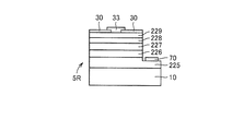
- the (electrode 70) was formed and formed into a chip having a size of 1 mm ⁇ 1 mm square (1 mm 2 ) to obtain an LED (light emitting diode) as the semiconductor device 5R.
- the n electrode (electrode 70) is formed on the same side as the p electrode (electrode 30).
- the light emission area of (semiconductor device 5R) is 15% smaller than the light emission area of the LED (semiconductor device 5) of Example 5.
- the light emission area is equal to the area of the p electrode (electrode 30) where the pad electrode 33 is not formed.
- the luminance of the LED of Example 5 was about 1.6 relative to the luminance of the LED of Comparative Example 2. It was twice as expensive.
- the Al layer existing under the n-type GaN layer 225 works as a reflective film, and the light emitting area can be increased by the vertical device structure, and the higher the current density, the more remarkable It is considered that the decrease in the internal quantum efficiency is advantageously working.
Landscapes
- Led Devices (AREA)
- Recrystallisation Techniques (AREA)
Abstract
Description
(実施形態1)
図1を参照して、本発明の一実施形態である半導体デバイス5は、支持基板60と、支持基板60上に配置された導電層50と、導電層50上に配置された少なくとも1層のIII族窒化物半導体層200とを含み、III族窒化物半導体層200のうち導電層50に隣接する導電層隣接III族窒化物半導体層200cは、n型導電性を有し、転位密度が1×107cm-2以下であり、酸素濃度が5×1018cm-3以下である。
本実施形態の半導体デバイス5における支持基板60は、半導体デバイス5のIII族窒化物半導体層200を支持するのに適したものであれば特に制限はないが、光透過性が高い観点からはサファイア支持基板、スピネル支持基板などが好ましく、導電性である観点からはSi支持基板、III族窒化物支持基板などが好ましく、III族窒化物半導体層200の熱膨張係数と同一または近似する熱膨張係数を有する観点からはIII族窒化物支持基板、SiC支持基板などが好ましい。また、支持基板60は単結晶でも多結晶でもよい。また、支持基板60と後述の導電層50との接合強度を高める観点から、支持基板60の表面に表面導電層65が形成されていてもよい。ここで、表面導電層65と後述の導電層50とは、化学組成が同一または近似していることが好ましい。
本実施形態の半導体デバイス5における導電層50は、半導体デバイス5の電極となり得るものであれば特に制限はないが、接触抵抗を下げる観点から、Al層、W層、Hf層などの金属層、また透光性を持たせたい場合にはITO(インジウムスズ酸化物)層、ZnO(亜鉛酸化物)層などの導電性酸化物層などが好ましい。さらに、密着性の向上のためおよび/またはパッド電極の形成のために、Tiおよび/またはAuの金属層を含んでいてもよい。
本実施形態の半導体デバイス5における少なくとも1層のIII族窒化物半導体層200は、その半導体デバイス5の機能を発現させるように形成されている。半導体デバイス5が電子デバイスの場合は、III族窒化物半導体層200は、たとえば、n+型半導体層、n-型半導体層などを含むことができる。また、半導体デバイス5が発光デバイスの場合は、III族窒化物半導体層200は、たとえば、発光層、電子ブロック層、コンタクト層などを含むことができる。
(実施形態2)
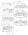
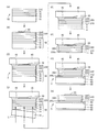
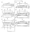
図2~3および6を参照して、本発明の別の実施形態である半導体デバイス5の製造方法は、下地基板10に第1のIII族窒化物半導体層210が貼り合わされた第1の複合基板1A,1Bを準備する工程(図2~3および6における(A))と、第1の複合基板1A,1Bの第1のIII族窒化物半導体層210上に少なくとも1層の第2のIII族窒化物半導体層220を成長させる工程(図2~3および6における(B))と、第2のIII族窒化物半導体層220に仮支持基板40を貼り合わせて第2の複合基板2を形成する工程(図2~3および6における(C))と、第2の複合基板2から下地基板10を除去する工程(図2~3および6における(D))と、第1のIII族窒化物半導体層210上に導電層50を形成する工程(図2における(E)、図3および6における(F))と、導電層50に支持基板60を貼り合わせて第3の複合基板3を形成する工程(図2における(F)、図3および6における(G))と、第3の複合基板3から仮支持基板40を除去する工程(図2における(G)、図3および6における(H))と、を含む。ここで、上記の第1のIII族窒化物半導体層210は、n型導電性を有し、転位密度が1×107cm-2以下であり、酸素濃度が5×1018cm-3以下である。
図2~3および6における(A)を参照して、第1の複合基板1A,1Bを準備する工程には、特に制限はないが、下地基板10と第1のIII族窒化物半導体層210との接合性を高めるとともに両者の分離を容易にする観点から、図7および図8のそれぞれに示すサブ工程を含むことが好ましい。
図7を参照して、第1の複合基板1Aを準備する工程について、以下に説明する。まず、図7(A)を参照して、下地基板10上にSiO2層12aを形成するサブ工程と、III族窒化物半導体基板20の一方の主表面上にSiO2層12bを形成した後、上記主表面から一定の深さの面Pにイオンを注入して面Pの領域を脆化させるサブ工程と、を含む。ここで、下地基板10は、特に制限はないが、後工程において第1のIII族窒化物半導体層210上に第2のIII族窒化物半導体層220を成長させる際に第1のIII族窒化物半導体層210にクラックを発生させない観点から、第1のIII族窒化物半導体層210と化学組成が同一または近似のIII族窒化物下地基板であることが好ましい。また、後工程において、下地基板10をレーザリフトオフで剥離する場合には、レーザが下地基板10を透過し第1のIII族窒化物半導体層210で吸収されるようにするために、下地基板10はサファイア下地基板、スピネル下地基板、酸化ガリウム下地基板などが好ましい。また、SiO2層12a,12bを形成する方法は、特に制限はなく、プラズマCVD(化学気相堆積)法、スパッタ法、真空蒸着法などが好適に挙げられる。
図8を参照して、第1の複合基板1Bを準備する工程について、以下に説明する。まず、図8(A)を参照して、下地基板10上に第1のSiO2層14、アモルファスSi層16および第2のSiO2層18aを順次形成するサブ工程と、III族窒化物半導体基板20の一方の主表面上に第2のSiO2層18bを形成した後、上記主表面から一定の深さの面Pにイオンを注入して面Pの領域を脆化させるサブ工程と、を含む。ここで、下地基板10は、特に制限はないが、後工程において第1のIII族窒化物半導体層210上に第2のIII族窒化物半導体層220を成長させる際に第1のIII族窒化物半導体層210にクラックを発生させない観点から、第1のIII族窒化物半導体層210と化学組成が同一または近似のIII族窒化物下地基板であることが好ましい。また、第1のSiO2層14、アモルファスSi層16および第2のSiO2層18a,18bを形成する方法は、特に制限はなく、プラズマCVD(化学気相堆積)法、スパッタ法、真空蒸着法などが好適に挙げられる。
図2~3および6における(B)を参照して、第2のIII族窒化物半導体層220の成長工程において、その成長方法は、第1のIII族窒化物半導体層210上に、少なくとも1層の第2のIII族窒化物半導体層220をエピタキシャル成長させることができる方法であれば特に制限はなく、MOVPE(有機金属気相成長)法、HVPE(ハイドライド気相成長)法、MBE(分子線成長)法、昇華法などの気相法、フラックス法、高窒素圧溶液法などの液相法などが好適に挙げられる。
第2のIII族窒化物半導体層220の成長工程の後、第2のIII族窒化物半導体層220の最外層上に、電極30を形成する工程(電極の形成工程)を含むことができる。
図2~3および6における(C)を参照して、第2の複合基板220の形成工程において、第2のIII族窒化物半導体層220と仮支持基板40とを貼り合わせる方法は、第2のIII族窒化物半導体層220を仮支持基板40で十分に支持することができかつ後工程で第2のIII族窒化物半導体層220から仮支持基板40を容易に除去できる方法であれば特に制限はなく、たとえば、ワックス42により貼り合わせる方法が好適に挙げられる。ワックス42などを用いることにより、第2のIII族窒化物半導体層220の最外層に電極30が形成されている場合であっても、第2のIII族窒化物半導体層220と仮支持基板40とを確実に貼り合わせることができる。
図2~3ならびに6における(C)および(D)を参照して、下地基板10の除去工程において、第2の複合基板2から下地基板10を除去する方法は、特に制限はないが、効率的に除去する観点から、レーザリフトオフ法が好ましい。レーザリフト法とは、レーザ光を複合基板に照射することにより、その複合基板を構成する一部の層の一部を分解することによりその複合基板の一部を分離する方法をいう。
図2(C)を参照して、第1の複合基板1Aを含む第2の複合基板2は、下地基板10、SiO2層12、第1のIII族窒化物半導体層210および第2のIII族窒化物半導体層220がこの順に積層された構造を有する。かかる構造は、下地基板10が、第1および第2のIII族窒化物半導体層210,220が吸収する波長の光を吸収しない基板、たとえば、サファイア下地基板、スピネル下地基板、酸化ガリウム下地基板などである場合に好適に採用される。
図3および6の(C)を参照して、第1の複合基板1Bを含む第2の複合基板2は、下地基板10、第1のSiO2層14、アモルファスSi層16、第2のSiO2層18、第1のIII族窒化物半導体層210および第2のIII族窒化物半導体層220がこの順に積層された構造を有する。かかる構造は、下地基板10が、第1および第2のIII族窒化物半導体層210,220が吸収する波長の光を吸収する基板、たとえば、III族窒化物下地基板などである場合に好適に採用される。
図2の(E)ならびに図3および6の(F)を参照して、導電層50の形成工程において、第1のIII族窒化物半導体層210上に導電層50を形成する方法には、導電層50の形成に適した方法であれば特に制限はなく、スパッタ法、真空蒸着法などが好適に挙げられる。
図2の(F)ならびに図3および6の(G)を参照して、第3の複合基板3の形成工程において、導電層50に支持基板60を貼り合わせる方法には、導電層50と確実に接合して導電層50ならびに第1および第2のIII族窒化物半導体層210,220を十分に支持できる方法であれば特に制限はなく、たとえば、貼り合わせ面をはんだにより接合するはんだ接合法、貼り合わせる面の表面を洗浄して直接貼り合わせた後700℃~1000℃に昇温して接合することによる直接接合法、プラズマやイオンなどで貼り合わせ面を活性化させ接合することによる表面活性化法などが好適に挙げられる。
図2の(F)および(G)ならびに図3および6の(G)および(H)を参照して、仮支持基板40の除去工程において、第3の複合基板3から仮支持基板40を除去する方法には、特に制限はなく、たとえば、仮支持基板40がワックス42により第2のIII族窒化物半導体層220に貼り合わされている場合には、そのワックス42を融解させることにより、仮支持基板40を除去することができる。
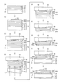
図4~5を参照して、本発明のさらに別の実施形態である半導体デバイス5の製造方法は、下地基板10に第1のIII族窒化物半導体層210が貼り合わされた第1の複合基板1Bを準備する工程(図4~5における(A))と、第1の複合基板1Bの第1のIII族窒化物半導体層210上に少なくとも1層の第2のIII族窒化物半導体層220を成長させる工程(図4~5における(B))と、第2のIII族窒化物半導体層220に仮支持基板40を貼り合わせて第2の複合基板2を形成する工程(図4~5における(C))と、第2の複合基板2から下地基板10を除去する工程(図4~5における(D))と、第1のIII族窒化物半導体層210を除去する工程(図4~5における(F))と、第2のIII族窒化物半導体層220上に導電層50を形成する工程(図4~5における(G))と、導電層50に支持基板60を貼り合わせて第4の複合基板4を形成する工程(図4~5における(H))と、第4の複合基板4から仮支持基板40を除去する工程(図4~5における(I))と、を含み、第2のIII族窒化物半導体層220のうち導電層50に隣接する導電層隣接III族窒化物半導体層200cは、n型導電性を有し、転位密度が1×107cm-2以下であり、酸素濃度が5×1017cm-3以下である。
図4~5の(A)~(E)を参照して、本発明のさらに別の実施形態である半導体デバイス5の製造方法における第1の複合基板1Bの準備工程、第2のIII族窒化物半導体層220の成長工程、第2の複合基板2の形成工程および下地基板10の除去工程は、それぞれ実施形態2の半導体デバイス5の製造方法における第1の複合基板1A,1Bの準備工程、第2のIII族窒化物半導体層220の成長工程、第2の複合基板2の形成工程および下地基板10の除去工程と同様である。
図4~5の(F)を参照して、第1のIII族窒化物半導体層210の除去工程において、第1のIII族窒化物半導体層210を除去する方法には、特に制限はなく、RIEなどのドライエッチングなどが好適に挙げられる。
図4~5の(G)を参照して、導電層50の形成工程において、第2のIII族窒化物半導体層220上に導電層50を形成する方法は、導電層50の形成に適した方法であれば特に制限はなく、スパッタ法、真空蒸着法などが好適に挙げられる。
図4~5の(H)を参照して、第4の複合基板4の形成工程において、導電層50に支持基板60を貼り合わせる方法には、導電層50と確実に接合して導電層50および第2のIII族窒化物半導体層220を十分に支持できる方法であれば特に制限はなく、たとえば、貼り合わせ面をはんだにより接合するはんだ接合法、貼り合わせる面の表面を洗浄して直接貼り合わせた後700℃~1000℃に昇温して接合することによる直接接合法、プラズマやイオンなどで貼り合わせ面を活性化させ接合することによる表面活性化法などが好適に挙げられる。
図4~5の(H)および(I)を参照して、仮支持基板40の除去工程において、第4の複合基板4から仮支持基板40を除去する方法には、特に制限はなく、たとえば、仮支持基板40がワックス42により第2のIII族窒化物半導体層220に貼り合わされている場合には、そのワックス42を融解させることにより、仮支持基板40を除去することができる。
1.第1の複合基板の準備
図2(A)を参照して、直径2インチ(5.08cm)で厚さ400μmのサファイア下地基板(下地基板10)に厚さ200nmのSiO2層12を介在させて厚さ150nmのGaN層(第1のIII族窒化物半導体層210)が貼り合わされた第1の複合基板1Aを準備した。ここで、GaN層(第1のIII族窒化物半導体層210)は、転位密度が5×106cm-2であり、酸素濃度が2×1018cm-3であった。転位密度はCL(カソードルミネッセンス)法により測定し、酸素濃度はSIMS(2次イオン質量分析)法より測定した。
図2(B)を参照して、上記の第1の複合基板1Aをアンモニア(NH3)ガスと水素(H2)ガスとの混合ガス中1050℃で10分間サーマルクリーニングした。かかる第1の複合基板1AのGaN層(第1のIII族窒化物半導体層210)上に、MOVPE法により、1100℃の条件で、第2のIII族窒化物半導体層220として、厚さ1μmでSi濃度が2×1018cm-3のn+型GaN層222および厚さが5μmでSi濃度が6×1015cm-3のn-型GaN層(ドリフト層)224を順次成長させた。さらに、n-型GaN層224上に、真空蒸着法により、直径200μmのNi層(厚さ50nm)/Au層(厚さ500nm)を形成し、600℃で2分間アニールすることにより合金化させることにより、ショットキー電極(電極30)を形成した。
図2(C)を参照して、上記の第2のIII族窒化物半導体層220および電極30とサファイア仮支持基板(仮支持基板40)とをワックス42で貼り合わることにより、第2の複合基板2を得た。
図2(C)および(D)を参照して、第2の複合基板2のサファイア下地基板(下地基板10)側から波長355nmのTHG-YAGレーザ光Lを照射して、レーザ光をGaN層(第1のIII族窒化物半導体層210)に吸収させ、GaN層(第1のIII族窒化物半導体層210)のサファイア下地基板(下地基板10)との界面近傍の部分を分解させることにより、サファイア下地基板(下地基板10)をリフトオフした。
図2(E)を参照して、露出したGaN層(第1のIII族窒化物半導体層210)の主表面に、真空蒸着法により、Al層(厚さ20nm)/Ti層(厚さ50nm)/Au層(厚さ500nm)で構成されるオーミック電極(導電層50)を形成した。
図2(F)を参照して、Si支持基板(支持基板60)の両主表面に、真空蒸着法によりAl層(厚さ20nm)/Ti層(厚さ50nm)/Au層(厚さ500nm)を形成し、400℃で10分間アニールすることにより合金化させて表面導電層65を形成した基板を準備した。かかる基板の表面導電層65と、オーミック電極(導電層50)とを、AuSnはんだにより貼り合わせることにより、第3の複合基板3を形成した。
図2(F)および(G)を参照して、第3の複合基板3においてワックス42を融解することにより、第3の複合基板3からサファイア仮支持基板(仮支持基板40)が除去されて、半導体デバイス5として、両主表面にAl層(厚さ20nm)/Ti層(厚さ50nm)/Au層(厚さ500nm)の合金層(表面導電層65)が形成されたSi支持基板(支持基板60)上に、Al層(厚さ20nm)/Ti層(厚さ50nm)/Au層(厚さ500nm)で構成されるオーミック電極(導電層50)、GaN層(第1のIII族窒化物半導体層210)、n+型GaN層222およびn-型GaN層(ドリフト層)224(第2のIII族窒化物半導体層220)、ならびにNi層(厚さ50nm)/Au層(厚さ500nm)の合金で構成されるショットキー電極(電極30)がこの順に形成されたSBD(ショットキーバリアダイオード)を得た。
/cm2における逆方向耐圧が400V、と高特性であった。
1.III族窒化物半導体層の成長
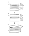
図9(A)を参照して、直径2インチ(5.08cm)で厚さ400μmのサファイア下地基板を水素(H2)ガス雰囲気中1100℃で10分間サーマルクリーニングした。その後、MOVPE法により、525℃の条件で、そのサファイア下地基板(下地基板10)上に厚さ25nmのGaNバッファ層(III族窒化物バッファ層290)を成長させた後、1100℃の条件で、GaNバッファ層(III族窒化物バッファ層290)上に厚さ1μmでSi濃度が2×1018cm-3のn+型GaN層222および厚さが5μmでSi濃度が6×1015cm-3のn-型GaN層(ドリフト層)224を順次成長させた。ここで、n+型GaN層222は、実施例1と同様に測定したところ、転位密度が1×109cm-2、サファイア下地基板(下地基板10)との界面近傍の部分における酸素濃度が1×1019cm-3であった。
図9(B)を参照して、この複合基板1Rのn-型GaN層224およびショットキー電極(電極30)とサファイア仮支持基板(仮支持基板40)とを、実施例1と同様にワックス42で貼り合わることにより、複合基板2Rを得た。
図9(B)および(C)を参照して、複合基板2Rのサファイア下地基板(下地基板10)側から実施例1と同様に波長355nmのTHG-YAGレーザ光Lを照射して、レーザ光をGaNバッファ層(III族窒化物バッファ層290)に吸収させて、これを分解させることにより、サファイア下地基板(下地基板10)をリフトオフした。
図9(D)を参照して、露出したn+型GaN層222の表面に、実施例1と同様にして、オーミック電極(導電層50)を形成した。
図9(E)を参照して、実施例1と同様にして、オーミック電極(導電層50)に、両主表面にAl層(厚さ20nm)/Ti層(厚さ50nm)/Au層(厚さ500nm)の合金層(表面導電層65)が形成されたSi支持基板(支持基板60)を貼り合わせることにより、複合基板3Rを得た。
図9(E)および(F)を参照して、実施例1と同様にして、複合基板3Rからサファイア仮支持基板(仮支持基板40)が除去することにより、半導体デバイス5Rとして、両主表面にAl層(厚さ20nm)/Ti層(厚さ50nm)/Au層(厚さ500nm)の合金層(表面導電層65)が形成されたSi支持基板(支持基板60)上に、Al層(厚さ20nm)/Ti層(厚さ50nm)/Au層(厚さ500nm)で構成されるオーミック電極(導電層50)、n+型GaN層222およびn-型GaN層(ドリフト層)224(III族窒化物半導体層200に対応)、ならびにNi層(厚さ50nm)/Au層(厚さ500nm)の合金で構成されるショットキー電極(電極30)がこの順に形成されたSBD(ショットキーバリアダイオード)を得た。
1.第1の複合基板の準備
図3(A)を参照して、直径2インチ(5.08cm)で厚さ400μmのGaN下地基板(下地基板10)に厚さ10nmの第1のSiO2層14、厚さ60nmのアモルファスSi層16および厚さ230nmの第2のSiO2層18を介在させて厚さ150nmのGaN層(第1のIII族窒化物半導体層210)が貼り合わされた第1の複合基板1Bを準備した。ここで、GaN層(第1のIII族窒化物半導体層210)は、転位密度が5×106cm-2であり、酸素濃度が2×1018cm-3であった。
図3(B)を参照して、実施例1と同様に、上記の第1の複合基板1Bをサーマルクリーニングした後、かかる第1の複合基板1BのGaN層(第1のIII族窒化物半導体層210)上に、MOVPE法により、1100℃の条件で、第2のIII族窒化物半導体層220として、厚さ1μmでSi濃度が2×1018cm-3のn+型GaN層222および
厚さが5μmでSi濃度が6×1015cm-3のn-型GaN層(ドリフト層)224を順次成長させた。さらに、実施例1と同様にして、n-型GaN層224上にショットキー電極(電極30)を形成した。
図3(C)を参照して、実施例1と同様に、上記の第2のIII族窒化物半導体層220および電極30とサファイア仮支持基板(仮支持基板40)とをワックス42で貼り合わることにより、第2の複合基板2を得た。
図3(C)および(D)を参照して、第2の複合基板2のGaN下地基板(下地基板10)側から波長532nmのSHG-YAGレーザ光Lを照射して、レーザ光LをアモルファスSi層16に吸収させて熱に変換させて、かかる熱によりGaN下地基(下地基板10)の第1のSiO2層14との界面近傍の部分を分解させることにより、GaN下地基板(下地基板10)をリフトオフした。ここで、第1のSiO2層14の厚さに比べて第2のSiO2層18の厚さが十分に大きいため、GaN層(第1のIII族窒化物半導体層210)ではなくGaN下地基板(下地基板10)を選択的に分解することができる。
図3(F)を参照して、露出したGaN層(第1のIII族窒化物半導体層210)の主表面に、実施例1と同様にして、オーミック電極(導電層50)を形成した。
図3(G)を参照して、実施例1と同様にして、オーミック電極(導電層50)に、両主表面にAl層(厚さ20nm)/Ti層(厚さ50nm)/Au層(厚さ500nm)の合金層(表面導電層65)が形成されたSi支持基板(支持基板60)を貼り合わせることにより、第3の複合基板3を形成した。
図3(G)および(H)を参照して、実施例1と同様にして、第3の複合基板3からサファイア仮支持基板(仮支持基板40)が除去することにより、半導体デバイス5として、両主表面にAl層(厚さ20nm)/Ti層(厚さ50nm)/Au層(厚さ500nm)の合金層(表面導電層65)が形成されたSi支持基板(支持基板60)上に、Al層(厚さ20nm)/Ti層(厚さ50nm)/Au層(厚さ500nm)で構成されるオーミック電極(導電層50)、GaN層(第1のIII族窒化物半導体層210)、n+型GaN層222およびn-型GaN層(ドリフト層)224(第2のIII族窒化物半導体層220)、ならびにNi層(厚さ50nm)/Au層(厚さ500nm)の合金で構成されるショットキー電極(電極30)がこの順に形成されたSBD(ショットキーバリアダイオード)を得た。
1.第1の複合基板の準備から下地基板の除去まで
図4(A)~(E)を参照して、実施例2と同様にして、第1の複合基板1Bを準備し、第2のIII族窒化物半導体層220の成長を成長させ、仮支持基板40を貼り合わせて第2の複合基板2を形成し、かかる第2の複合基板2から下地基板10を除去し、さらに、GaN層(第1のIII族窒化物半導体層210)上に残っている第1のSiO2層14、アモルファスSi層16および第2のSiO2層18をフッ酸硝酸混合溶液によるウェットエッチングにより除去した(図4(E))。
図4(F)を参照して、GaN層(第1のIII族窒化物半導体層210)をRIEにより除去した。かかるRIEにより、露出したn+型GaN層222は、転位密度が5×106cm-2、酸素濃度が5×1016cm-3と結晶性が非常に高く、その表面のRMS粗さが40nmと小さく平坦であった。
図4(G)を参照して、露出したn+型GaN層222の主表面に、実施例1と同様にして、オーミック電極(導電層50)を形成した。
図4(H)を参照して、実施例1と同様にして、オーミック電極(導電層50)に、両主表面にAl層(厚さ20nm)/Ti層(厚さ50nm)/Au層(厚さ500nm)の合金層(表面導電層65)が形成されたSi支持基板(支持基板60)を貼り合わせることにより、第4の複合基板4を形成した。
図4(H)および(I)を参照して、実施例1と同様にして、第4の複合基板4からサファイア仮支持基板(仮支持基板40)が除去することにより、半導体デバイス5として、両主表面にAl層(厚さ20nm)/Ti層(厚さ50nm)/Au層(厚さ500nm)の合金層(表面導電層65)が形成されたSi支持基板(支持基板60)上に、Al層(厚さ20nm)/Ti層(厚さ50nm)/Au層(厚さ500nm)で構成されるオーミック電極(導電層50)、n+型GaN層222およびn-型GaN層(ドリフト層)224(第2のIII族窒化物半導体層220)、ならびにNi層(厚さ50nm)/Au層(厚さ500nm)の合金で構成されるショットキー電極(電極30)がこの順に形成されたSBD(ショットキーバリアダイオード)を得た。
1.第1の複合基板の準備
図5(A)を参照して、実施例2と同様にして、第1の複合基板1Bを準備した。
図5(B)を参照して、実施例1と同様に、上記の第1の複合基板1Bをサーマルクリーニングした後、かかる第1の複合基板1BのGaN層(第1のIII族窒化物半導体層210)上に、第2のIII族窒化物半導体層220として、厚さ20nmでSi濃度が2×1018cm-3のn+型Al0.04Ga0.96N層221、厚さ1μmでSi濃度が2×1018cm-3のn+型GaN層222および厚さが5μmでSi濃度が6×1015cm-3のn-型GaN層(ドリフト層)224を順次成長させた。ここで、n+型Al0.04Ga0.96N層221は、転位密度が5×106cm-2、酸素濃度が8×1016cm-3であった。さらに、実施例1と同様にして、n-型GaN層224上にショットキー電極(電極30)を形成した。
図5(C)~(I)を参照して、実施例3と同様にして、仮支持基板40を貼り合わせて第2の複合基板2を形成し、かかる第2の複合基板2から下地基板10を除去し、さらに、第1のSiO2層14、アモルファスSi層16、第2のSiO2層18およびGaN層(第1のIII族窒化物半導体層210)を除去し、露出したn+型Al0.04Ga0.96N層221の表面にオーミック電極(導電層50)を形成し、このオーミック電極(導電層50)にAl層(厚さ20nm)/Ti層(厚さ50nm)/Au層(厚さ500nm)の合金層(表面導電層65)が形成されたSi支持基板(支持基板60)を貼り合わせることにより第4の複合基板4を形成し、かかる第4の複合基板4からサファイア仮支持基板(仮支持基板40)を除去することにより、半導体デバイス5たるSBDを得た。
1.第1の複合基板の準備
図6(A)を参照して、実施例2と同様にして、第1の複合基板1Bを準備した。
図6(B)を参照して、実施例1と同様に、上記の第1の複合基板1Bをサーマルクリーニングした後、かかる第1の複合基板1BのGaN層(第1のIII族窒化物半導体層210)上に、MOVPE法により、第2のIII族窒化物半導体層220として、厚さ2μmのn型GaN層225、厚さ100nmのn型In0.02Ga0.98N緩衝層226、厚さ3nmのIn0.15Ga0.85N井戸層と厚さ15nmのGaN障壁層で形成される3重の多重量子井戸(MQW)構造を有する発光層227、厚さ20nmのp型Al0.18Ga0.82N電子ブロック層228および厚さ50nmのp型GaNコンタクト層229を形成した。ここで、n型In0.02Ga0.98N緩衝層226およびGaN障壁層は840℃で成長させ、In0.15Ga0.85N井戸層は780℃で成長させ、その他の層は1100℃で成長させた。
図6(C)~(I)を参照して、実施例2と同様にして、仮支持基板40を貼り合わせて第2の複合基板2を形成し、かかる第2の複合基板2から下地基板10を除去し、さらに、第1のSiO2層14、アモルファスSi層16および第2のSiO2層18を除去し、露出したGaN層(第1のIII族窒化物半導体層210)の表面にオーミック電極(導電層50)を形成し、このオーミック電極(導電層50)にAl層(厚さ20nm)/Ti層(厚さ50nm)/Au層(厚さ500nm)の合金層(表面導電層65)が形成されたSi支持基板(支持基板60)を貼り合わせることにより第3の複合基板3を形成し、かかる第3の複合基板3からサファイア仮支持基板(仮支持基板40)を除去し、1mm×1mm角(1mm2)の大きさにチップ化することにより、半導体デバイス5たるLED(発光ダイオード)を得た。
図10を参照して、サファイア下地基板上に、MOVPE法により、厚さ5μmのn型GaN層225、厚さ100nmのn型In0.02Ga0.98N緩衝層226、厚さ3nmのIn0.15Ga0.85N井戸層と厚さ15nmのGaN障壁層で形成される3重の多重量子井戸(MQW)構造を有する発光層227、厚さ20nmのp型Al0.18Ga0.82N電子ブロック層228および厚さ50nmのp型GaNコンタクト層229を形成した。ここで、n型In0.02Ga0.98N緩衝層226およびGaN障壁層は840℃で成長させ、In0.15Ga0.85N井戸層は780℃で成長させ、その他の層は1100℃で成長させた。
Claims (6)
- 支持基板(60)と、前記支持基板(60)上に配置された導電層(50)と、前記導電層(50)上に配置された少なくとも1層のIII族窒化物半導体層(200)と、を含み、
前記III族窒化物半導体層(200)のうち前記導電層(50)に隣接する導電層隣接III族窒化物半導体層(200c)は、n型導電性を有し、転位密度が1×107cm-2以下であり、酸素濃度が5×1018cm-3以下である半導体デバイス。 - 前記導電層隣接III族窒化物半導体層(200c)の酸素濃度が5×1017cm-3以下である請求項1に記載の半導体デバイス。
- 前記導電層隣接III族窒化物半導体層(200c)は、III族窒化物を構成するIII族元素としてAlを含む請求項2に記載の半導体デバイス。
- 前記導電層隣接III族窒化物半導体層(200c)は、III族窒化物を構成するIII族元素としてAlを含む請求項1に記載の半導体デバイス。
- 下地基板(10)に第1のIII族窒化物半導体層(210)が貼り合わされた第1の複合基板(1A,1B)を準備する工程と、
前記第1の複合基板(1A,1B)の前記第1のIII族窒化物半導体層(210)上に少なくとも1層の第2のIII族窒化物半導体層(220)を成長させる工程と、
前記第2のIII族窒化物半導体層(220)に仮支持基板(40)を貼り合わせて第2の複合基板(2)を形成する工程と、
前記第2の複合基板(2)から前記下地基板(10)を除去する工程と、
前記第1のIII族窒化物半導体層(210)上に導電層(50)を形成する工程と、
前記導電層(50)に支持基板(60)を貼り合わせて第3の複合基板(3)を形成する工程と、
前記第3の複合基板(3)から前記仮支持基板(40)を除去する工程と、を含み、
前記第1のIII族窒化物半導体層(210)は、n型導電性を有し、転位密度が1×107cm-2以下であり、酸素濃度が5×1018cm-3以下である半導体デバイスの製造方法。 - 下地基板(10)に第1のIII族窒化物半導体層(210)が貼り合わされた第1の複合基板(1A,1B)を準備する工程と、
前記第1の複合基板(1A,1B)の前記第1のIII族窒化物半導体層(210)上に少なくとも1層の第2のIII族窒化物半導体層(220)を成長させる工程と、
前記第2のIII族窒化物半導体層(220)に仮支持基板(40)を貼り合わせて第2の複合基板(2)を形成する工程と、
前記第2の複合基板(2)から前記下地基板(10)を除去する工程と、
前記第1のIII族窒化物半導体層(210)を除去する工程と、
前記第2のIII族窒化物半導体層(220)上に導電層(50)を形成する工程と、
前記導電層(50)に支持基板(60)を貼り合わせて第4の複合基板(4)を形成する工程と、
前記第4の複合基板(4)から前記仮支持基板(40)を除去する工程と、を含み、
前記第2のIII族窒化物半導体層(220)のうち前記導電層(50)に隣接する導電層隣接III族窒化物半導体層(200c)は、n型導電性を有し、転位密度が1×107cm-2以下であり、酸素濃度が5×1017cm-3以下である半導体デバイスの製造方法。
Priority Applications (1)
| Application Number | Priority Date | Filing Date | Title |
|---|---|---|---|
| CN2012800010445A CN102822998A (zh) | 2011-02-15 | 2012-01-19 | 半导体器件及其制造方法 |
Applications Claiming Priority (2)
| Application Number | Priority Date | Filing Date | Title |
|---|---|---|---|
| JP2011-029867 | 2011-02-15 | ||
| JP2011029867A JP5333479B2 (ja) | 2011-02-15 | 2011-02-15 | 半導体デバイスの製造方法 |
Publications (1)
| Publication Number | Publication Date |
|---|---|
| WO2012111379A1 true WO2012111379A1 (ja) | 2012-08-23 |
Family
ID=46636211
Family Applications (1)
| Application Number | Title | Priority Date | Filing Date |
|---|---|---|---|
| PCT/JP2012/051062 Ceased WO2012111379A1 (ja) | 2011-02-15 | 2012-01-19 | 半導体デバイスおよびその製造方法 |
Country Status (6)
| Country | Link |
|---|---|
| US (1) | US8884306B2 (ja) |
| JP (1) | JP5333479B2 (ja) |
| KR (1) | KR20120114403A (ja) |
| CN (1) | CN102822998A (ja) |
| TW (1) | TW201246593A (ja) |
| WO (1) | WO2012111379A1 (ja) |
Cited By (3)
| Publication number | Priority date | Publication date | Assignee | Title |
|---|---|---|---|---|
| WO2014109137A1 (ja) * | 2013-01-11 | 2014-07-17 | Dowaエレクトロニクス株式会社 | 発光素子及びその製造方法 |
| WO2020235074A1 (ja) * | 2019-05-23 | 2020-11-26 | 三菱電機株式会社 | 半導体基板の製造方法および半導体装置の製造方法 |
| US11309686B2 (en) | 2017-06-20 | 2022-04-19 | Sony Corporation | Surface emitting laser and method of manufacturing the same |
Families Citing this family (21)
| Publication number | Priority date | Publication date | Assignee | Title |
|---|---|---|---|---|
| JP5734935B2 (ja) * | 2012-09-20 | 2015-06-17 | 株式会社東芝 | 半導体装置及びその製造方法 |
| US9082692B2 (en) | 2013-01-02 | 2015-07-14 | Micron Technology, Inc. | Engineered substrate assemblies with epitaxial templates and related systems, methods, and devices |
| JP2014209508A (ja) * | 2013-04-16 | 2014-11-06 | 住友電気工業株式会社 | はんだ付半導体デバイス、実装はんだ付半導体デバイス、はんだ付半導体デバイスの製造方法および実装方法 |
| JP2015097239A (ja) * | 2013-11-15 | 2015-05-21 | 住友電気工業株式会社 | 半導体デバイスおよびその製造方法 |
| TW201530757A (zh) * | 2013-12-30 | 2015-08-01 | 維克儀器公司 | 用於以結晶氮化物為主之裝置中的工程基板 |
| KR101758082B1 (ko) * | 2013-12-30 | 2017-07-17 | 한국전자통신연구원 | 질화물 반도체 소자의 제조 방법 |
| JP2016032038A (ja) * | 2014-07-29 | 2016-03-07 | 住友化学株式会社 | 窒化物半導体ウエハおよびその製造方法 |
| CN105590839B (zh) * | 2016-03-22 | 2018-09-14 | 安徽三安光电有限公司 | 氮化物底层、发光二极管及底层制备方法 |
| JP7242552B2 (ja) * | 2017-12-11 | 2023-03-20 | ソニーセミコンダクタソリューションズ株式会社 | 垂直共振器型面発光レーザ素子の製造方法 |
| WO2020011117A1 (zh) * | 2018-07-12 | 2020-01-16 | 江西兆驰半导体有限公司 | 一种提高光提取效率的紫外发光二极管芯片及其制作方法 |
| JP2021012900A (ja) * | 2019-07-03 | 2021-02-04 | パナソニックIpマネジメント株式会社 | Iii族窒化物系半導体レーザ素子 |
| JP7391326B2 (ja) * | 2019-12-26 | 2023-12-05 | 株式会社ノベルクリスタルテクノロジー | 半導体装置 |
| JP2022132130A (ja) * | 2021-02-26 | 2022-09-07 | 日亜化学工業株式会社 | 半導体発光素子とその製造方法 |
| KR102570675B1 (ko) * | 2021-12-03 | 2023-08-25 | 웨이브로드 주식회사 | 비발광 3족 질화물 반도체 적층체를 제조하는 방법 |
| KR102591148B1 (ko) * | 2021-10-01 | 2023-10-19 | 웨이브로드 주식회사 | 비발광 3족 질화물 반도체 적층체를 제조하는 방법 |
| KR102591150B1 (ko) * | 2021-12-30 | 2023-10-19 | 웨이브로드 주식회사 | 비발광 3족 질화물 반도체 소자를 제조하는 방법 |
| KR102597905B1 (ko) * | 2022-10-24 | 2023-11-03 | 웨이브로드 주식회사 | 그룹3족 질화물 반도체 템플릿의 제조 방법 및 이에 의해 제조된 그룹3족 질화물 반도체 템플릿 |
| KR102681487B1 (ko) * | 2022-08-30 | 2024-07-04 | 웨이브로드 주식회사 | 그룹3족 질화물 전력반도체 소자의 제조 방법 및 이에 따라 제조된 그룹3족 질화물 전력반도체 소자 |
| KR102621470B1 (ko) * | 2022-12-20 | 2024-01-09 | 웨이브로드 주식회사 | 에피택시 다이를 이용한 그룹3족 질화물 전력반도체 소자 제조 방법 |
| CN116332678B (zh) * | 2023-05-30 | 2023-08-11 | 中南大学 | 一种在碳材料表面制备碳化钽涂层的方法 |
| WO2025154830A1 (ko) * | 2024-01-15 | 2025-07-24 | 웨이브로드 주식회사 | 그룹3족 질화물 전력반도체 소자의 제조 방법 및 이에 따라 제조된 그룹3족 질화물 전력반도체 소자 |
Citations (6)
| Publication number | Priority date | Publication date | Assignee | Title |
|---|---|---|---|---|
| WO2008091010A1 (ja) * | 2007-01-26 | 2008-07-31 | Shin-Etsu Handotai Co., Ltd. | 発光素子及びその製造方法 |
| JP2009120465A (ja) * | 2007-10-24 | 2009-06-04 | Sumitomo Electric Ind Ltd | 半絶縁性窒化物半導体基板とその製造方法並びに窒化物半導体エピタキシャル基板及び電界効果トランジスタ |
| JP2009260391A (ja) * | 2009-08-05 | 2009-11-05 | Sumitomo Electric Ind Ltd | Iii族窒化物半導体層貼り合わせ基板および半導体デバイスの製造方法 |
| JP2010056100A (ja) * | 2008-08-26 | 2010-03-11 | Sumitomo Electric Ind Ltd | ショットキーバリアダイオード |
| JP2010182936A (ja) * | 2009-02-06 | 2010-08-19 | Sumitomo Electric Ind Ltd | 複合基板、エピタキシャル基板、半導体デバイス及び複合基板の製造方法 |
| JP2010232625A (ja) * | 2009-03-03 | 2010-10-14 | Sumitomo Electric Ind Ltd | 貼り合わせ基板の製造方法 |
Family Cites Families (5)
| Publication number | Priority date | Publication date | Assignee | Title |
|---|---|---|---|---|
| KR100610639B1 (ko) | 2005-07-22 | 2006-08-09 | 삼성전기주식회사 | 수직 구조 질화갈륨계 발광다이오드 소자 및 그 제조방법 |
| JP2007134388A (ja) | 2005-11-08 | 2007-05-31 | Sharp Corp | 窒化物系半導体素子とその製造方法 |
| KR100730072B1 (ko) | 2005-12-06 | 2007-06-20 | 삼성전기주식회사 | 수직구조 질화갈륨계 발광 다이오드 소자 및 그 제조방법 |
| KR100815225B1 (ko) * | 2006-10-23 | 2008-03-19 | 삼성전기주식회사 | 수직구조 발광다이오드 소자 및 그 제조방법 |
| JP4458116B2 (ja) | 2007-05-30 | 2010-04-28 | 住友電気工業株式会社 | エピタキシャル層成長用iii族窒化物半導体層貼り合わせ基板および半導体デバイス |
-
2011
- 2011-02-15 JP JP2011029867A patent/JP5333479B2/ja active Active
-
2012
- 2012-01-19 US US13/353,707 patent/US8884306B2/en active Active
- 2012-01-19 WO PCT/JP2012/051062 patent/WO2012111379A1/ja not_active Ceased
- 2012-01-19 KR KR1020127023480A patent/KR20120114403A/ko not_active Ceased
- 2012-01-19 CN CN2012800010445A patent/CN102822998A/zh active Pending
- 2012-02-03 TW TW101103580A patent/TW201246593A/zh unknown
Patent Citations (6)
| Publication number | Priority date | Publication date | Assignee | Title |
|---|---|---|---|---|
| WO2008091010A1 (ja) * | 2007-01-26 | 2008-07-31 | Shin-Etsu Handotai Co., Ltd. | 発光素子及びその製造方法 |
| JP2009120465A (ja) * | 2007-10-24 | 2009-06-04 | Sumitomo Electric Ind Ltd | 半絶縁性窒化物半導体基板とその製造方法並びに窒化物半導体エピタキシャル基板及び電界効果トランジスタ |
| JP2010056100A (ja) * | 2008-08-26 | 2010-03-11 | Sumitomo Electric Ind Ltd | ショットキーバリアダイオード |
| JP2010182936A (ja) * | 2009-02-06 | 2010-08-19 | Sumitomo Electric Ind Ltd | 複合基板、エピタキシャル基板、半導体デバイス及び複合基板の製造方法 |
| JP2010232625A (ja) * | 2009-03-03 | 2010-10-14 | Sumitomo Electric Ind Ltd | 貼り合わせ基板の製造方法 |
| JP2009260391A (ja) * | 2009-08-05 | 2009-11-05 | Sumitomo Electric Ind Ltd | Iii族窒化物半導体層貼り合わせ基板および半導体デバイスの製造方法 |
Cited By (6)
| Publication number | Priority date | Publication date | Assignee | Title |
|---|---|---|---|---|
| WO2014109137A1 (ja) * | 2013-01-11 | 2014-07-17 | Dowaエレクトロニクス株式会社 | 発光素子及びその製造方法 |
| JP2014135433A (ja) * | 2013-01-11 | 2014-07-24 | Dowa Electronics Materials Co Ltd | 発光素子の製造方法 |
| US11309686B2 (en) | 2017-06-20 | 2022-04-19 | Sony Corporation | Surface emitting laser and method of manufacturing the same |
| WO2020235074A1 (ja) * | 2019-05-23 | 2020-11-26 | 三菱電機株式会社 | 半導体基板の製造方法および半導体装置の製造方法 |
| JPWO2020235074A1 (ja) * | 2019-05-23 | 2021-10-21 | 三菱電機株式会社 | 半導体基板の製造方法および半導体装置の製造方法 |
| JP7186872B2 (ja) | 2019-05-23 | 2022-12-09 | 三菱電機株式会社 | 半導体基板の製造方法および半導体装置の製造方法 |
Also Published As
| Publication number | Publication date |
|---|---|
| JP2012169481A (ja) | 2012-09-06 |
| CN102822998A (zh) | 2012-12-12 |
| JP5333479B2 (ja) | 2013-11-06 |
| US20120205661A1 (en) | 2012-08-16 |
| TW201246593A (en) | 2012-11-16 |
| US8884306B2 (en) | 2014-11-11 |
| KR20120114403A (ko) | 2012-10-16 |
Similar Documents
| Publication | Publication Date | Title |
|---|---|---|
| JP5333479B2 (ja) | 半導体デバイスの製造方法 | |
| JP4638958B1 (ja) | 半導体素子の製造方法 | |
| TWI395341B (zh) | Group III nitride semiconductor crystal and its manufacturing method, Group III nitride semiconductor device and manufacturing method thereof, and light emitting machine | |
| KR20100008123A (ko) | 이중 히트 씽크층으로 구성된 지지대를 갖춘 고성능수직구조의 반도체 발광소자 | |
| US20040140474A1 (en) | Semiconductor light-emitting device, method for fabricating the same and method for bonding the same | |
| JP2010186829A (ja) | 発光素子の製造方法 | |
| KR20130029455A (ko) | GaN계 반도체 디바이스의 제조방법 | |
| TW200818248A (en) | Substrate having thin film of GaN joined thereon and method of fabricating the same, and a GaN-based semiconductor device and method of fabricating the same | |
| JP2012114263A (ja) | 半導体素子およびその製造方法 | |
| JP2011066398A (ja) | 半導体素子およびその製造方法 | |
| JP5771968B2 (ja) | 半導体デバイスの製造方法、エピ成長用積層支持基板およびデバイス用積層支持基板 | |
| KR101428066B1 (ko) | 수직구조 그룹 3족 질화물계 반도체 발광다이오드 소자 및이의 제조 방법 | |
| KR100832102B1 (ko) | 발광소자용 구조체 및 발광소자의 제조 방법 | |
| KR101480551B1 (ko) | 수직구조 그룹 3족 질화물계 반도체 발광다이오드 소자 및이의 제조 방법 | |
| JP2010040692A (ja) | 窒化物系半導体素子及びその製造方法 | |
| JP2007221056A (ja) | 窒化物半導体発光素子およびその製造方法 | |
| JP2010226023A (ja) | 窒化物系化合物半導体層を支持基板上に有する基板生産物を製造する方法、及び半導体デバイスの製造方法 | |
| KR101231118B1 (ko) | 반도체 발광소자용 지지기판 및 상기 지지기판을 이용한고성능 수직구조의 반도체 발광소자 | |
| KR101499954B1 (ko) | 수직구조 그룹 3족 질화물계 반도체 발광다이오드 소자 및제조방법 | |
| US8987026B2 (en) | Semiconductor light emitting device | |
| CN107452861A (zh) | 一种紫外led芯片及其制备方法 | |
| JP2008117824A (ja) | 窒化物系半導体素子の製造方法 | |
| JP2010161160A (ja) | 半導体発光素子 | |
| JP2015040136A (ja) | Iii族窒化物膜の製造方法およびiii族窒化物半導体デバイスの製造方法 | |
| KR20070046174A (ko) | 금속 기판 위의 GaN계 발광 소자 |
Legal Events
| Date | Code | Title | Description |
|---|---|---|---|
| WWE | Wipo information: entry into national phase |
Ref document number: 201280001044.5 Country of ref document: CN |
|
| ENP | Entry into the national phase |
Ref document number: 20127023480 Country of ref document: KR Kind code of ref document: A |
|
| 121 | Ep: the epo has been informed by wipo that ep was designated in this application |
Ref document number: 12746564 Country of ref document: EP Kind code of ref document: A1 |
|
| NENP | Non-entry into the national phase |
Ref country code: DE |
|
| 122 | Ep: pct application non-entry in european phase |
Ref document number: 12746564 Country of ref document: EP Kind code of ref document: A1 |