WO2012105209A1 - Ledのフラッシュ生成装置およびledのフラッシュ生成方法 - Google Patents
Ledのフラッシュ生成装置およびledのフラッシュ生成方法 Download PDFInfo
- Publication number
- WO2012105209A1 WO2012105209A1 PCT/JP2012/000545 JP2012000545W WO2012105209A1 WO 2012105209 A1 WO2012105209 A1 WO 2012105209A1 JP 2012000545 W JP2012000545 W JP 2012000545W WO 2012105209 A1 WO2012105209 A1 WO 2012105209A1
- Authority
- WO
- WIPO (PCT)
- Prior art keywords
- circuit
- path
- inductive element
- capacitor
- led
- Prior art date
Links
Images


Classifications
-
- H—ELECTRICITY
- H05—ELECTRIC TECHNIQUES NOT OTHERWISE PROVIDED FOR
- H05B—ELECTRIC HEATING; ELECTRIC LIGHT SOURCES NOT OTHERWISE PROVIDED FOR; CIRCUIT ARRANGEMENTS FOR ELECTRIC LIGHT SOURCES, IN GENERAL
- H05B45/00—Circuit arrangements for operating light-emitting diodes [LED]
- H05B45/30—Driver circuits
- H05B45/37—Converter circuits
- H05B45/3725—Switched mode power supply [SMPS]
- H05B45/38—Switched mode power supply [SMPS] using boost topology
-
- H—ELECTRICITY
- H05—ELECTRIC TECHNIQUES NOT OTHERWISE PROVIDED FOR
- H05B—ELECTRIC HEATING; ELECTRIC LIGHT SOURCES NOT OTHERWISE PROVIDED FOR; CIRCUIT ARRANGEMENTS FOR ELECTRIC LIGHT SOURCES, IN GENERAL
- H05B45/00—Circuit arrangements for operating light-emitting diodes [LED]
- H05B45/30—Driver circuits
- H05B45/37—Converter circuits
- H05B45/3725—Switched mode power supply [SMPS]
- H05B45/375—Switched mode power supply [SMPS] using buck topology
-
- G—PHYSICS
- G03—PHOTOGRAPHY; CINEMATOGRAPHY; ANALOGOUS TECHNIQUES USING WAVES OTHER THAN OPTICAL WAVES; ELECTROGRAPHY; HOLOGRAPHY
- G03B—APPARATUS OR ARRANGEMENTS FOR TAKING PHOTOGRAPHS OR FOR PROJECTING OR VIEWING THEM; APPARATUS OR ARRANGEMENTS EMPLOYING ANALOGOUS TECHNIQUES USING WAVES OTHER THAN OPTICAL WAVES; ACCESSORIES THEREFOR
- G03B2215/00—Special procedures for taking photographs; Apparatus therefor
- G03B2215/05—Combinations of cameras with electronic flash units
- G03B2215/0564—Combinations of cameras with electronic flash units characterised by the type of light source
- G03B2215/0567—Solid-state light source, e.g. LED, laser
-
- Y—GENERAL TAGGING OF NEW TECHNOLOGICAL DEVELOPMENTS; GENERAL TAGGING OF CROSS-SECTIONAL TECHNOLOGIES SPANNING OVER SEVERAL SECTIONS OF THE IPC; TECHNICAL SUBJECTS COVERED BY FORMER USPC CROSS-REFERENCE ART COLLECTIONS [XRACs] AND DIGESTS
- Y02—TECHNOLOGIES OR APPLICATIONS FOR MITIGATION OR ADAPTATION AGAINST CLIMATE CHANGE
- Y02B—CLIMATE CHANGE MITIGATION TECHNOLOGIES RELATED TO BUILDINGS, e.g. HOUSING, HOUSE APPLIANCES OR RELATED END-USER APPLICATIONS
- Y02B20/00—Energy efficient lighting technologies, e.g. halogen lamps or gas discharge lamps
- Y02B20/30—Semiconductor lamps, e.g. solid state lamps [SSL] light emitting diodes [LED] or organic LED [OLED]
Definitions
- the present invention relates to an LED flash generation device and an LED flash generation method. More specifically, the present invention relates to a flash generation device and a flash generation method for charging a large-capacity capacitor from a power source and generating a flash of an LED by the charged energy.
- Patent Document 1 discloses an LED flash light emitting device. With reference to FIG. 1, the main part shown by FIG. 6 and FIG. 7 of patent document 1 is demonstrated roughly.
- the energy stored in the battery is charged into the large-capacity capacitor 920 by the constant current / constant voltage charging circuit 910, and the energy stored in the large-capacity capacitor 920 is boosted by the flash LED boost constant current circuit 930.
- the boosted energy is supplied to the LED as a load.
- the present invention has been made in view of such problems, and an object of the present invention is to provide an LED flash generation device with a small energy loss and a small system area for forming a circuit.
- One aspect of the present invention is an LED flash generation device including an input power supply, a capacitor, an inductive element connected to the capacitor, and a switching circuit, the switching circuit from the input power supply to the inductive element Forming a path to the capacitor, stepping down the energy of the input power supply, charging the capacitor, and forming a path from the capacitor and the inductive element to the LED to charge the capacitor.
- the LED flash generation device is characterized in that the energy is boosted and then output to the LED.
- the switching circuit has first, second, third, and fourth terminals, the input power source is connected to the first terminal, and the inductive element includes the capacitor and the second terminal
- the LED is connected to the third terminal, the fourth terminal is connected to the ground, and the switching circuit is connected between the first terminal and the second terminal.
- the inductive element, the first path, and the second path form a step-down circuit
- the inductive element, the second path, and the third path form a step-up circuit. Can be configured.
- the switching circuit conducts the first path and the second path in a complementary manner, performs a step-down operation together with the inductive element, and complements the second path and the third path. Can be boosted together with the inductive element.
- the switching circuit can block the third path while performing the step-down operation, and can block the first path while performing the step-up operation.
- the second path may include a transistor connected between the inductive element and the ground.
- the first path may include a transistor connected between the first terminal and the second terminal.
- the third path may include a diode connected between the second terminal and the third terminal.
- Another aspect of the present invention is an LED flash generation method, wherein a path from an input power source to an inductive element and a capacitor connected to the inductive element is formed, and the energy of the input power source is stepped down. Charging a capacitor; and forming a path from the capacitor and the inductive element to the LED, boosting energy charged in the capacitor, and then outputting to the LED. LED flash generation method.
- an LED flash generation device including an input power source, a capacitor, an inductive element connected between the input power source and one end of the capacitor, and one end connected to the capacitor. And a step-up circuit including the inductive element connected between the one end of the capacitor and the one end of the LED.
- the inductive element includes both the step-down circuit and the step-up circuit.
- a flash generation device characterized by being an element.
- an LED flash drive circuit including a control circuit, a first transistor whose switching is controlled by a drive signal output from the control circuit, and the control circuit and a ground.
- a control circuit a first transistor whose switching is controlled by a drive signal output from the control circuit, and the control circuit and a ground.
- a constant current source provided at one end of the first transistor, connected to an input power supply, provided at the other end of the first transistor, and connected to a booster circuit
- the second transistor having one end connected to the inductive element and the other end connected to the ground.
- a flash drive circuit of the LED which is a part of.
- the same dielectric element can be a constituent element of both the step-down circuit and the step-up circuit.
- the system area can be significantly reduced as compared with the conventional flash generator in which the constant current / constant voltage charging circuit and the booster circuit exist independently.
- the large-capacity capacitor is charged from the input power supply via the step-down circuit. For this reason, energy loss can be suppressed as compared with a conventional flash generation device in which a large-capacity capacitor is charged via a constant current / constant voltage charging circuit.
- FIG. 1 is a diagram showing a configuration of a conventional flash light emitting device.
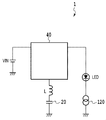
- FIG. 2 is a diagram showing the configuration of the LED flash generation device of the present invention.
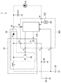
- FIG. 3 is a diagram illustrating a configuration of an LED flash generation apparatus according to an embodiment of the present invention.
- FIG. 4 is a diagram illustrating a configuration example of a control circuit of the LED flash generation device according to the embodiment of the present invention.
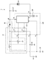
- FIG. 5 is a diagram for explaining the operation (during charging) of the LED flash generation device according to the embodiment of the present invention.
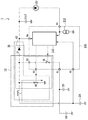
- FIG. 6 is a diagram for explaining the operation (during charging) of the LED flash generation device according to an embodiment of the present invention.
- FIG. 7 is a diagram for explaining the operation (during discharge) of the LED flash generation device according to one embodiment of the present invention.
- FIG. 8 is a diagram for explaining an operation (during discharge) of the LED flash generation device according to the embodiment of the present invention.
- FIG. 2 is a diagram showing the configuration of the LED flash generation device of the present invention.
- the flash generation device 1 includes an input power source VIN, a large-capacitance capacitor 20, an induction element L connected to the large-capacity capacitor 20, and a switching circuit 40.
- the switching circuit 40 forms a path according to the step-down and step-up operations as follows. A path (first path) from the input power source VIN to the induction element L and the large-capacitance capacitor 20 is formed, and the energy of the input power source VIN is stepped down. The large-capacitance capacitor 20 is charged with the reduced voltage. Further, a path (second path) from the large capacity capacitor 20 and the inductive element L to the LED is formed, and the energy charged in the large capacity capacitor 20 is boosted. After boosting, energy is output to the LED.
- the LED has one end connected to the switching circuit 40 and the other end connected to the constant current source 120.
- the switching circuit 40 When the switching circuit 40 performs a step-down operation, the switching circuit 40 forms a path (first path) from the input power supply VIN to the induction element L and the large-capacitance capacitor 20, and inputs the energy of the input power supply VIN to the induction element L. The voltage is stepped down to charge the large capacity capacitor 20 with the energy.
- the switching circuit 40 forms a large-capacitance capacitor 20 and a path (second path) from the same inductive element L used for the step-down operation to the LED (second path) when performing the step-up operation.
- the energy charged in 20 is input to the inductive element L to be boosted, and the energy is output to the LED.
- the path formed by the switching circuit 40 means that not only a static DC path is formed but also a path capable of transmitting energy related to the inductive element L is formed. Please note that. As will be described in detail later with reference to FIGS. 5 to 8, in the flash generation device of the present invention, since the inductive element L functions as a part of the DC / DC converter, a part of the above path is repeatedly turned on / off. Works to do. Therefore, the above-described path also operates so as to be opened and closed intermittently.
- the switching circuit 40 forms a path in which the direction of energy input to the induction element L can be set in both directions. With the configuration of the switching circuit 40, both the step-down operation and the step-up operation can be performed using one inductive element L. For this reason, since two different operations can be performed using one common circuit element, the system area can be reduced.
- the flash generation device of the present invention performs a step-down operation and a step-up operation using an inductive element and has low loss, it is possible to reduce energy loss.
- FIG. 3 is a diagram showing a configuration of an LED flash generation apparatus according to an embodiment of the present invention.
- the step-down circuit 10 is constituted by a path from the other end of the circuit to the ground.
- the voltage is boosted by the inductive element L, the path from the other end of the inductive element L to the ground, and the path from the other end of the inductive element L to the LED in the switching circuit 40.
- a circuit 30 is configured.
- a path is formed between the input power source VIN and the other end of the inductive element L, energy from the input power source VIN is input to the inductive element L, and the large-capacitance capacitor 20 is charged with the energy.
- the energy charged in the large-capacitance capacitor 20 is charged in the induction element L, a path is formed between the other end of the induction element L and the LED, and the energy is discharged to the LED.
- the flash generation device 1 has a path (first path) for inputting energy from the input power source VIN to the inductive element L and a path (second path) for outputting energy from the inductive element L to the LED. Pass).
- the direction of the current flowing through the inductive element L is reversed between charging and discharging the energy of the large-capacitance capacitor 20.
- the inductive element L can be shared as one component having the functions of both the step-down circuit 10 and the step-up circuit 30. Since different functions can be performed by using one shared element, the system area can be reduced.
- the flash generation device of the present invention uses an inductive element in the step-down circuit 10 and has low loss, it is possible to reduce energy loss.
- the first transistor M1 is connected between the input power source VIN and the other end of the inductive element L (the opposite end of the large-capacitance capacitor 20). A path is formed between VIN and the other end of the inductive element.
- the second transistor M2 is connected between the other end of the inductive element L and the ground, and a path between the other end of the inductive element L and the ground is formed.
- a diode D1 is connected between the other end of the inductive element L and the LED, and a path between the other end of the inductive element L and the LED is configured.
- the inductive element L and the LED can be selectively conducted to each other.
- the second transistor M2 is connected between the other end of the inductive element L and the ground, so that the second transistor M2 is shared as a constituent element of both the step-down circuit 10 and the step-up circuit 30. be able to.
- the system area can be further reduced.
- the flash generation device 1 of the present invention Compared with the conventional flash generation device in which the constant current / constant voltage charging circuit 910 and the booster circuit 930 shown in FIG. 1 are configured independently, the flash generation device 1 of the present invention further increases the system area. It becomes possible to make it significantly smaller.
- the flash generation device 1 also includes a flash drive circuit 100 for charging and discharging the large-capacitance capacitor 20.
- the flash light emitting device of Patent Document 1 is the same in that a control circuit E for charging / discharging the large-capacity capacitor 920 (in the constant current / constant voltage charging circuit 910) is provided.
- the configuration in which the inductive element L and the second transistor M2 are also shared, which is unique to the present embodiment, can significantly reduce the area of the circuit components that constitute the system as compared with the prior art.
- the first transistor M1 and the second transistor M2 are a P-channel MOS transistor and an N-channel MOS transistor, respectively. It may be a MOS transistor. In this case, the polarities of the drive signals given to the gates of the first transistor M1 and the second transistor M2 are reversed.
- the path between the other end of the inductive element L and the LED is a diode D1.
- the transistor is not limited to the diode D1, and may be a transistor.
- a drive signal is applied to each gate so that the transistor replacing the diode D1 is turned off when the step-down circuit 10 operates, and is turned on and off complementarily with the second transistor M2 when the step-up circuit 30 operates. It ’s fine.
- the flash generation device 1 shown in FIG. 3 charges the large-capacitance capacitor 20 from the input power source VIN via the step-down circuit 10. For this reason, it is possible to suppress energy loss as compared with the conventional flash generation device in which the large-capacity capacitor 920 is charged via the constant current / constant voltage charging circuit 910.
- the “large-capacity capacitor” is a capacitor having a large capacitance value such as an electric double layer capacitor, a super capacitor, or an ultra capacitor, and is preferably a capacitor of 0.1 F or more and 10,000 F or less.
- the constant current source 120 is connected between the other end of the LED and the ground has been described so far, but it is also possible to drive the LED with a constant voltage.
- the LED is driven with a large current, it is preferable to drive at a constant current in order to prevent the current from flowing beyond the recommended maximum current of the LED and shortening the lifetime.
- the flash drive circuit 100 includes a control circuit 110, a first transistor M1 whose switching is controlled by a drive signal output from the control circuit 110, and a constant current source 120 connected between the control circuit 110 and the ground.
- the flash drive circuit 100 includes six terminals described below. That is, a first terminal N1 provided at one end of the first transistor M1 and connected to the input power supply VIN, and a second terminal provided at the other end of the first transistor M1 and connected to the booster circuit 30.
- the terminal N2, the third terminal N3 for controlling the switching of the second transistor M2, which is a common component of the step-down circuit 10 and the step-up circuit 30, and the constant current source 120 are connected to the LED.
- the step-down circuit 10 and the step-up circuit 30 have the same common transistor (specifically, the second transistor M2) and the inductive element (specifically, the inductive element L). It has been explained from the viewpoint that it is included as a component. However, it can be explained from a different point of view.
- the step-down circuit 10 can also be regarded as a configuration in which the first transistor M1 is added to the second transistor M2 and the inductive element L that are part of the step-up circuit 30.
- the step-down circuit 10 operates as a step-down DC / DC converter by a drive signal from the control circuit 110 of the flash drive circuit 100.
- the booster circuit 30 operates as a boost DC / DC converter by different drive signals from the control circuit 110 of the flash drive circuit 100.
- the flash drive circuit 100 can operate the booster circuit 30 by such a configuration and operation of the flash generation device. Further, the flash drive circuit 100 can operate the step-down circuit 10 including the inductive element L and the second transistor M2, which are part of the step-up circuit 30, and the first transistor M1.
- FIG. 4 is a diagram illustrating a configuration example of the control circuit 110 of the LED flash generation device according to the embodiment of the present invention.
- the control circuit 110 is connected in series between the fifth terminal N5 and the ground, divides the voltage of the large-capacitance capacitor 20 and outputs a divided voltage from the common connection portion, and the divided voltage and
- An error amplifier circuit AMP1 that amplifies the difference from the reference voltage VREF1 and outputs an error voltage, an oscillation circuit OSC that outputs a triangular wave, and an error voltage output from the error amplifier circuit AMP1 and the triangular wave are compared to output a PWM signal.
- the comparison circuit CMP1 the error amplification circuit AMP2 that amplifies the difference between the voltage at the fourth terminal and the reference voltage VREF2, and outputs an error voltage, and the error voltage output from the error amplification circuit AMP2 and the triangular wave are compared to obtain PWM.
- the comparison circuit CMP2 that outputs a signal, the voltage of the large-capacitance capacitor 20, the output voltage, and the PWM signal that the comparison circuits CPM1 and CMP2 output And a drive circuit 130 for outputting a driving signal for controlling each switching of the first transistor M1 and the second transistor M2 and respectively input.
- the reference voltage VREF1 is a voltage corresponding to a desired voltage of the large-capacitance capacitor 20, and the reference voltage VREF2 is a voltage corresponding to a desired output voltage so that an appropriate bias voltage is applied to the LED. .
- the PWM signal output from the comparison circuit CMP1 is a signal for stepping down the input power supply VIN
- the PWM signal output from the comparison circuit CMP2 is a signal for stepping up the voltage of the large-capacitance capacitor 20.
- the drive circuit 130 When the drive circuit 130 steps down the voltage of the input power supply VIN to charge the large-capacitance capacitor 20, the drive circuit 130 selects the PWM signal output from the comparison circuit CMP1 and applies this to the first transistor M1 and the second transistor M2. Outputs the PWM signal. At this time, the first transistor M1 and the second transistor M2 are complementarily turned on and off according to the duty of the PWM signal.
- the drive circuit 130 When the drive circuit 130 boosts the voltage of the large-capacitance capacitor 20 and outputs an output voltage to the LED, the drive circuit 130 selects the PWM signal output from the comparison circuit CMP2, and outputs this PWM signal to the second transistor M2. A high level signal is output to the first transistor M1. At this time, the second transistor M2 is turned on / off according to the duty of the PWM signal. Since it is a P-channel MOS transistor and a high level signal is input, the first transistor M1 is turned off.
- the drive circuit 130 monitors the voltage of the large-capacitance capacitor 20 from the fifth terminal N5, and the PWM signal output from the comparison circuit CMP1 so that the step-down operation is performed when the charge voltage is lower than a desired charge level. Select. Further, control is performed so that the large-capacitance capacitor 20 does not exceed the breakdown voltage.
- the drive circuit 130 selects the output voltage of the comparison circuit CMP2 and monitors the cathode voltage of the LED of the fourth terminal N4. When the voltage is lower than the reference voltage VREF2, the drive circuit 130 increases the output voltage, and the voltage is the reference voltage. When the voltage is higher than the voltage VREF2, control is performed so that the boosting operation is performed while lowering the output voltage.
- the drive circuit 130 monitors the output voltage from the sixth terminal N6, turns off the first transistor M1 and the second transistor M2 in the event of an overvoltage, and stops the boosting operation. ⁇ Description of operation>
- the operation of charging power from the input power source VIN to the large-capacity capacitor 20 via the step-down circuit 10 will be described.
- the first transistor M1 and the second transistor M2 are complementarily turned on and off to step down the input voltage and charge the large capacity capacitor 20.
- the voltage at both ends of the diode D1 is turned off below the threshold, the path between the other end of the inductive element L and the LED is blocked.
- FIG. 5 is a diagram for explaining the operation at the time of charging of the LED flash generation device according to the embodiment of the present invention.
- the step-down circuit 10 uses the flash drive circuit 100 to turn on the first transistor M1 and turn off the second transistor M2.
- a current flows from the input power source VIN to the large-capacitance capacitor 20 through the first transistor M1 and the inductive element L, and the inductive element L is charged with energy.
- the current path at this time is indicated by a broken-line arrow.
- the step-down circuit 10 conducts a path between the input power source VIN and the inductive element L, cuts off a path between the inductive element L and the ground, and charges the inductive element L with energy.
- FIG. 6 is another diagram for explaining the operation at the time of charging of the LED flash generation device according to the embodiment of the present invention.
- the step-down circuit 10 uses the flash drive circuit 100 to turn off the first transistor M1 and turn on the second transistor M2. Then, a current flows from the ground to the large-capacitance capacitor 20 through the second transistor M2 and the inductive element L. The current path at this time is indicated by a broken-line arrow.
- the step-down circuit 10 cuts off the path between the input power source VIN and the inductive element L and conducts the path between the inductive element L and the ground so that the energy charged in the inductive element L has a large capacity.
- the capacitor 20 is charged.
- the operation in which the path between the input power source VIN and the inductive element L and the path between the inductive element L and ground are complementarily conducted is repeated.
- the charging / discharging of the energy to the induction element L is repeated, and the large-capacitance capacitor 20 is charged with the energy obtained by stepping down the input power source VIN.
- the charging state of the large-capacitance capacitor 20 is fed back from the fifth terminal N5 to the control circuit 110, so that when the large-capacity capacitor 20 reaches a desired charge level, the switching of the first transistor M1 is stopped and the charging operation is performed. End.
- the flash generator of the present invention uses the conventional constant current / constant voltage charging circuit 910 by charging the large-capacitance capacitor 20 through the step-down circuit 10 using the inductive element L. Energy loss is greatly reduced compared to the device. Specifically, when the power supply voltage is 3.7 V, the average current supplied from the input power supply VIN is 0.5 A, and the efficiency of the step-down circuit 10 is 80%, the charging by the conventional constant current / constant voltage charging circuit 910 is performed. Table 1 below shows the energy loss generated by charging and the energy loss generated by charging by the step-down circuit 10 according to the present invention.
- the charging current to the large-capacitance capacitor 920 is also 0.5 A.
- Charging current to the large-capacitance capacitor average current supplied from the power supply ⁇ power supply voltage ⁇ efficiency of the step-down circuit / large-capacitance capacitor voltage Therefore, charging current to the large-capacity capacitor is as shown in Table 2 below.
- the large capacity is obtained via the step-down circuit 10 as compared with the conventional flash generation device that charges the large capacity capacitor 920 via the constant current / constant voltage charging circuit 910.
- the flash generator 1 according to the present invention that charges the capacitor 20, more charging current can be supplied to the large-capacity capacitor 20. Therefore, the charging time can be greatly shortened.
- the operation of boosting the power charged in the large-capacitance capacitor 20 using the booster circuit 30 and supplying it to the LED as a load will be described.
- the voltage of the large-capacitance capacitor 20 can be boosted and supplied to the LED by switching the second transistor M2 and turning off the first transistor M1. At this time, the path between the input power supply and the other end of the induction element L is blocked.
- FIG. 7 is a view for explaining the operation at the time of discharging of the LED flash generation device according to the embodiment of the present invention.
- the booster circuit 30 turns on the second transistor M ⁇ b> 2 by the flash drive circuit 100. Then, a current flows from the large-capacitance capacitor 20 to the ground through the induction element L, and the energy is charged in the induction element L. The current path at this time is indicated by a broken-line arrow. Further, at this time, the energy stored in the output capacitor COUT is discharged to the LED, so that a current flows through the LED.
- the booster circuit 30 conducts a path between the inductive element L and the ground to charge the inductive element L with energy.
- FIG. 8 is another diagram for explaining the operation at the time of discharging of the LED flash generation device according to the embodiment of the present invention.
- the booster circuit 30 turns off the second transistor M ⁇ b> 2 by the flash drive circuit 100.
- a current flows from the large-capacitance capacitor 20 to the LED and the output capacitor COUT through the inductive element L and the diode D1.
- the current path at this time is indicated by a broken-line arrow.
- the booster circuit 30 supplies the energy charged in the inductive element L to the LED by blocking the path between the inductive element L and the ground and conducting the path between the inductive element L and the LED. To do.
- the flash generation apparatus of the present invention can reduce energy loss and system area by the above-described configuration and operation.
- the present invention can be used in a flash generation device that generates a flash by an LED.
Abstract
Description
<フラッシュ生成装置>
図2は、本発明のLEDのフラッシュ生成装置の構成を示す図である。
<フラッシュ駆動回路>
<動作説明>

全エネルギー
=電源電圧×電源から供給する平均電流
定電流・定電圧充電回路使用時のロス
=(電源電圧-コンデンサ電圧)×電源から供給する平均電流
降圧回路使用時のロス
=全エネルギー×(1-降圧回路の効率)
表1より、本発明のフラッシュ生成装置は、エネルギーのロスが大幅に少ないことがわかる。
大容量コンデンサへの充電電流
=電源から供給する平均電流×電源電圧×降圧回路の効率/大容量コンデンサ電圧
となるので、大容量コンデンサへの充電電流は、下記表2の通りとなる。

つまり、電源から供給する平均電流が同じ場合、定電流・定電圧充電回路910を介して大容量コンデンサ920に充電していた従来のフラッシュ生成装置と比較して、降圧回路10を介して大容量コンデンサ20に充電する本発明に係るフラッシュ生成装置1では、大容量コンデンサ20へより多く充電電流を供給することできる。したがって、充電時間も大幅に短縮することができる。
10 降圧回路
20 大容量コンデンサ
30 昇圧回路
40 スイッチング回路
100 フラッシュ駆動回路
110 コントロール回路
120 定電流源
VIN 入力電源
M1 第1のトランジスタ
M2 第2のトランジスタ
L 誘導素子
N1 第1の端子
N2 第2の端子
N3 第3の端子
N4 第4の端子
N5 第5の端子
N6 第6の端子
R1、R2 抵抗
AMP1、AMP2 誤差増幅回路
CMP1、CMP2 比較回路
OSC 発振回路
130 ドライブ回路
Claims (10)
- LEDのフラッシュ生成装置において、
入力電源と、
コンデンサと、
前記コンデンサに接続された誘導素子と、
スイッチング回路と、
を備え、
前記スイッチング回路は、
前記入力電源から前記誘導素子、前記コンデンサへのパスを形成して、前記入力電源のエネルギーを降圧した後、前記コンデンサに充電すると共に、前記コンデンサ、前記誘導素子から前記LEDへのパスを形成して、前記コンデンサに充電されたエネルギーを昇圧した後、前記LEDに出力することを特徴とするLEDのフラッシュ生成装置。 - 前記スイッチング回路は、第1、第2、第3、および第4の端子を有し、
前記入力電源は、前記第1の端子に接続され、
前記誘導素子は、前記コンデンサと前記第2の端子との間に接続され、
前記LEDは、前記第3の端子に接続され、
前記第4の端子は、グラウンドに接続され、
前記スイッチング回路は、
前記第1の端子と前記第2の端子との間の第1のパスを形成し、前記第2の端子と第4の端子との間の第2のパスを形成し、前記第2の端子と前記第3の端子との間の第3のパスを形成し、
前記誘導素子と前記第1のパスと前記第2のパスとが、降圧回路を構成し、前記誘導素子と前記第2のパスと前記第3のパスとが、昇圧回路を構成することを特徴とする請求項1に記載のLEDのフラッシュ生成装置。 - 前記スイッチング回路は、
前記第1のパスと前記第2のパスを相補的に導通して、前記誘導素子とともに降圧動作を行い、前記第2のパスと前記第3のパスを相補的に導通して、前記誘導素子とともに昇圧動作を行うことを特徴とする請求項2記載のLEDのフラッシュ生成装置。 - 前記スイッチング回路は、
前記降圧動作を行う間は前記第3のパスを遮断し、前記昇圧動作を行う間は前記第1のパスを遮断することを特徴とする請求項3に記載のLEDのフラッシュ生成装置。 - 前記第2のパスは、
前記誘導素子と前記グラウンドとの間に接続されたトランジスタを含むことを特徴とする請求項2乃至4のいずれかに記載のLEDのフラッシュ生成装置。 - 前記第1のパスは、
前記第1の端子と前記第2の端子との間に接続されたトランジスタを含むことを特徴とする請求項2乃至5のいずれかに記載のLEDのフラッシュ生成装置。 - 前記第3のパスは、
前記第2の端子と前記第3の端子との間に接続されたダイオードを含むことを特徴とする請求項2乃至6のいずれかに記載のLEDのフラッシュ生成装置。 - LEDのフラッシュ生成方法において、
入力電源から誘導素子、誘導素子に接続されたコンデンサへのパスを形成して、前記入力電源のエネルギーを降圧した後、前記コンデンサに充電するステップと、
前記コンデンサ、前記誘導素子から前記LEDへのパスを形成して、前記コンデンサに充電されたエネルギーを昇圧した後、前記LEDに出力するステップと、
を備えたことを特徴とするLEDのフラッシュ生成方法。 - LEDのフラッシュ生成装置において、
入力電源と、
コンデンサと、
前記入力電源と前記コンデンサの一端との間に接続され、一端が前記コンデンサに接続された誘導素子を含む降圧回路と、
前記コンデンサの前記一端と前記LEDの一端との間に接続され、前記誘導素子を含む昇圧回路と、
を備え、
前記誘導素子は、前記降圧回路および前記昇圧回路の両方の構成素子であることを特徴とするフラッシュ生成装置。 - LEDのフラッシュ駆動回路において、
コントロール回路と、
前記コントロール回路が出力する駆動信号によってスイッチングが制御される第1のトランジスタと、
前記コントロール回路とグラウンドとの間に接続された定電流源と、
前記第1のトランジスタの一端に設けられ、入力電源に接続するための第1の端子と、
前記第1のトランジスタの他端に設けられ、昇圧回路に接続するための第2の端子と、
第2のトランジスタのスイッチングを駆動信号により制御するための第3の端子と、
前記定電流源をLEDと接続するための第4の端子と、
を備え、
一端がコンデンサに接続された誘導素子と、一端が前記誘導素子に接続され、他端がグラウンドに接続された前記第2のトランジスタとが、前記昇圧回路の一部であることを特徴とするLEDのフラッシュ駆動回路。
Priority Applications (3)
| Application Number | Priority Date | Filing Date | Title |
|---|---|---|---|
| JP2012533818A JP5432384B2 (ja) | 2011-02-01 | 2012-01-27 | Ledのフラッシュ生成装置およびledのフラッシュ生成方法 |
| CN201280004078.XA CN103250468B (zh) | 2011-02-01 | 2012-01-27 | Led 的闪光生成装置和led 的闪光生成方法 |
| US13/823,842 US20130181632A1 (en) | 2011-02-01 | 2012-01-27 | Flash Generating Device for LED and Flash Generating Method for LED |
Applications Claiming Priority (2)
| Application Number | Priority Date | Filing Date | Title |
|---|---|---|---|
| JP2011020209 | 2011-02-01 | ||
| JP2011-020209 | 2011-02-01 |
Publications (1)
| Publication Number | Publication Date |
|---|---|
| WO2012105209A1 true WO2012105209A1 (ja) | 2012-08-09 |
Family
ID=46602435
Family Applications (1)
| Application Number | Title | Priority Date | Filing Date |
|---|---|---|---|
| PCT/JP2012/000545 WO2012105209A1 (ja) | 2011-02-01 | 2012-01-27 | Ledのフラッシュ生成装置およびledのフラッシュ生成方法 |
Country Status (4)
| Country | Link |
|---|---|
| US (1) | US20130181632A1 (ja) |
| JP (1) | JP5432384B2 (ja) |
| CN (1) | CN103250468B (ja) |
| WO (1) | WO2012105209A1 (ja) |
Families Citing this family (4)
| Publication number | Priority date | Publication date | Assignee | Title |
|---|---|---|---|---|
| JP6386217B2 (ja) | 2012-09-12 | 2018-09-05 | センシティ システムズ インコーポレイテッド | 感知応用のためのネットワーク接続された照明インフラストラクチャ |
| US9582671B2 (en) | 2014-03-06 | 2017-02-28 | Sensity Systems Inc. | Security and data privacy for lighting sensory networks |
| EP2911474B1 (en) | 2014-02-20 | 2017-08-02 | Dialog Semiconductor (UK) Limited | High voltage converter without auxiliary winding |
| CN107430317B (zh) * | 2015-03-02 | 2020-07-03 | 保富图公司 | 闪光发生器以及具有识别电子器件的闪光灯头和延伸电缆 |
Citations (3)
| Publication number | Priority date | Publication date | Assignee | Title |
|---|---|---|---|---|
| JPS5741625A (en) * | 1980-08-25 | 1982-03-08 | Minolta Camera Co Ltd | Power source circuit of flash device |
| JPH11135274A (ja) * | 1997-10-30 | 1999-05-21 | Toshiba Tec Corp | Led照明装置 |
| JP2010182883A (ja) * | 2009-02-05 | 2010-08-19 | Denso Corp | 発光ダイオード駆動回路 |
Family Cites Families (20)
| Publication number | Priority date | Publication date | Assignee | Title |
|---|---|---|---|---|
| JPH0374091A (ja) * | 1989-08-12 | 1991-03-28 | Matsushita Electric Works Ltd | 放電灯点灯装置 |
| JPH0678527A (ja) * | 1992-08-26 | 1994-03-18 | Nec Kansai Ltd | 駆動電圧供給装置とその集積回路 |
| JPH10164859A (ja) * | 1996-11-26 | 1998-06-19 | Matsushita Electric Works Ltd | 電源装置 |
| JP4288553B2 (ja) * | 2000-07-25 | 2009-07-01 | 富士フイルム株式会社 | カメラのストロボ装置 |
| JP3900817B2 (ja) * | 2000-10-30 | 2007-04-04 | 松下電工株式会社 | 無電極放電灯点灯装置 |
| US20040091255A1 (en) * | 2002-11-11 | 2004-05-13 | Eastman Kodak Company | Camera flash circuit with adjustable flash illumination intensity |
| US7969121B2 (en) * | 2005-02-02 | 2011-06-28 | Cap-Xx Limited | Power supply that uses a supercapacitive device |
| JP4704103B2 (ja) * | 2005-05-16 | 2011-06-15 | ローム株式会社 | 定電流駆動回路、それを利用した電子機器および発光ダイオードの駆動方法 |
| JP2007080771A (ja) * | 2005-09-16 | 2007-03-29 | Nec Lighting Ltd | 照明用低圧電源回路、照明装置および照明用低圧電源出力方法 |
| US8174209B2 (en) * | 2008-01-30 | 2012-05-08 | Texas Instruments Deutschland Gmbh | DC-DC converter and method for minimizing battery peak pulse loading |
| JP2010177115A (ja) * | 2009-01-30 | 2010-08-12 | Minebea Co Ltd | 希ガス放電灯点灯装置 |
| DE102009003852B4 (de) * | 2009-04-30 | 2013-05-16 | Lear Corporation Gmbh | Gleichspannungswandler |
| US8686667B2 (en) * | 2010-01-26 | 2014-04-01 | Panasonic Corporation | Lighting power source with controlled charging operation for driving capacitor |
| JP2012009772A (ja) * | 2010-06-28 | 2012-01-12 | Toshiba Lighting & Technology Corp | 電源装置および照明器具 |
| JP2012049273A (ja) * | 2010-08-26 | 2012-03-08 | Toshiba Lighting & Technology Corp | 直流電源装置およびledランプシステム |
| EP2649716A4 (en) * | 2010-12-09 | 2017-11-22 | Indice Semiconductor Inc. | Power supply control system and device |
| JP5942314B2 (ja) * | 2011-02-22 | 2016-06-29 | パナソニックIpマネジメント株式会社 | 点灯装置および、これを用いた照明器具 |
| US8810144B2 (en) * | 2012-05-02 | 2014-08-19 | Cree, Inc. | Driver circuits for dimmable solid state lighting apparatus |
| JP6130692B2 (ja) * | 2013-03-07 | 2017-05-17 | 株式会社小糸製作所 | 半導体光源点灯回路および車両用灯具 |
| KR20140141907A (ko) * | 2013-06-03 | 2014-12-11 | 주식회사 포스코엘이디 | 고출력 led 구동회로를 구비한 led 조명장치 |
-
2012
- 2012-01-27 JP JP2012533818A patent/JP5432384B2/ja not_active Expired - Fee Related
- 2012-01-27 US US13/823,842 patent/US20130181632A1/en not_active Abandoned
- 2012-01-27 CN CN201280004078.XA patent/CN103250468B/zh active Active
- 2012-01-27 WO PCT/JP2012/000545 patent/WO2012105209A1/ja active Application Filing
Patent Citations (3)
| Publication number | Priority date | Publication date | Assignee | Title |
|---|---|---|---|---|
| JPS5741625A (en) * | 1980-08-25 | 1982-03-08 | Minolta Camera Co Ltd | Power source circuit of flash device |
| JPH11135274A (ja) * | 1997-10-30 | 1999-05-21 | Toshiba Tec Corp | Led照明装置 |
| JP2010182883A (ja) * | 2009-02-05 | 2010-08-19 | Denso Corp | 発光ダイオード駆動回路 |
Also Published As
| Publication number | Publication date |
|---|---|
| CN103250468B (zh) | 2014-10-29 |
| US20130181632A1 (en) | 2013-07-18 |
| CN103250468A (zh) | 2013-08-14 |
| JPWO2012105209A1 (ja) | 2014-07-03 |
| JP5432384B2 (ja) | 2014-03-05 |
Similar Documents
| Publication | Publication Date | Title |
|---|---|---|
| JP4781744B2 (ja) | 電源装置及びこれを用いた電気機器 | |
| JP4871970B2 (ja) | 電源装置 | |
| JP4762722B2 (ja) | 電源装置及びこれを備えた電子機器 | |
| US20200336063A1 (en) | Multi-level power converter with improved transient load response | |
| US20170047839A1 (en) | Switched Capacitors with Inverted Break-Before-Make without External Filtering Load Capacitor | |
| JP2009055722A (ja) | チャージポンプ方式電源回路 | |
| JP5432384B2 (ja) | Ledのフラッシュ生成装置およびledのフラッシュ生成方法 | |
| US6307359B1 (en) | DC-DC converter powered by doubled output voltage | |
| JP2010004691A (ja) | フラッシュ用電源装置 | |
| JP2008060492A (ja) | 発光素子駆動装置 | |
| JP2010063299A (ja) | 昇圧形コンバータ | |
| JP5660936B2 (ja) | 発光素子駆動回路 | |
| US7586212B2 (en) | Multi-output power supply apparatus | |
| JP2009118698A (ja) | Led駆動用電源回路及びその駆動方法 | |
| JP4739901B2 (ja) | スイッチング電源装置およびその制御回路、ならびにそれを用いた電子機器 | |
| TWI411210B (zh) | 具電荷泵控制之單電感多重輸出直流轉換器 | |
| JP6559901B2 (ja) | 電子制御装置 | |
| JP5418817B2 (ja) | Dc−dc変換装置 | |
| JP2009231644A (ja) | 発光素子駆動回路 | |
| CN110663164A (zh) | 具有多个功率模式的功率转换器预驱动器系统 | |
| JP2010098915A (ja) | チャージポンプ回路 | |
| JP2011135738A (ja) | Dc−dcコンバータ | |
| JP2009027919A (ja) | チャージポンプ回路 | |
| JP2009165236A (ja) | スイッチングレギュレータおよびその制御方法 | |
| Surkanti et al. | High-efficiency, high-dimming ratio LED driver |
Legal Events
| Date | Code | Title | Description |
|---|---|---|---|
| WWE | Wipo information: entry into national phase |
Ref document number: 2012533818 Country of ref document: JP |
|
| 121 | Ep: the epo has been informed by wipo that ep was designated in this application |
Ref document number: 12741962 Country of ref document: EP Kind code of ref document: A1 |
|
| WWE | Wipo information: entry into national phase |
Ref document number: 13823842 Country of ref document: US |
|
| NENP | Non-entry into the national phase |
Ref country code: DE |
|
| 122 | Ep: pct application non-entry in european phase |
Ref document number: 12741962 Country of ref document: EP Kind code of ref document: A1 |