WO2012086517A1 - 発光素子ユニットおよび発光素子パッケージ - Google Patents
発光素子ユニットおよび発光素子パッケージ Download PDFInfo
- Publication number
- WO2012086517A1 WO2012086517A1 PCT/JP2011/079055 JP2011079055W WO2012086517A1 WO 2012086517 A1 WO2012086517 A1 WO 2012086517A1 JP 2011079055 W JP2011079055 W JP 2011079055W WO 2012086517 A1 WO2012086517 A1 WO 2012086517A1
- Authority
- WO
- WIPO (PCT)
- Prior art keywords
- side electrode
- emitting element
- electrode
- element unit
- light emitting
- Prior art date
- Legal status (The legal status is an assumption and is not a legal conclusion. Google has not performed a legal analysis and makes no representation as to the accuracy of the status listed.)
- Ceased
Links
Images









Classifications
-
- H—ELECTRICITY
- H10—SEMICONDUCTOR DEVICES; ELECTRIC SOLID-STATE DEVICES NOT OTHERWISE PROVIDED FOR
- H10H—INORGANIC LIGHT-EMITTING SEMICONDUCTOR DEVICES HAVING POTENTIAL BARRIERS
- H10H20/00—Individual inorganic light-emitting semiconductor devices having potential barriers, e.g. light-emitting diodes [LED]
- H10H20/80—Constructional details
- H10H20/85—Packages
- H10H20/8506—Containers
-
- H—ELECTRICITY
- H10—SEMICONDUCTOR DEVICES; ELECTRIC SOLID-STATE DEVICES NOT OTHERWISE PROVIDED FOR
- H10W—GENERIC PACKAGES, INTERCONNECTIONS, CONNECTORS OR OTHER CONSTRUCTIONAL DETAILS OF DEVICES COVERED BY CLASS H10
- H10W20/00—Interconnections in chips, wafers or substrates
- H10W20/20—Interconnections within wafers or substrates, e.g. through-silicon vias [TSV]
-
- F—MECHANICAL ENGINEERING; LIGHTING; HEATING; WEAPONS; BLASTING
- F21—LIGHTING
- F21K—NON-ELECTRIC LIGHT SOURCES USING LUMINESCENCE; LIGHT SOURCES USING ELECTROCHEMILUMINESCENCE; LIGHT SOURCES USING CHARGES OF COMBUSTIBLE MATERIAL; LIGHT SOURCES USING SEMICONDUCTOR DEVICES AS LIGHT-GENERATING ELEMENTS; LIGHT SOURCES NOT OTHERWISE PROVIDED FOR
- F21K9/00—Light sources using semiconductor devices as light-generating elements, e.g. using light-emitting diodes [LED] or lasers
- F21K9/20—Light sources comprising attachment means
- F21K9/27—Retrofit light sources for lighting devices with two fittings for each light source, e.g. for substitution of fluorescent tubes
-
- H—ELECTRICITY
- H10—SEMICONDUCTOR DEVICES; ELECTRIC SOLID-STATE DEVICES NOT OTHERWISE PROVIDED FOR
- H10D—INORGANIC ELECTRIC SEMICONDUCTOR DEVICES
- H10D1/00—Resistors, capacitors or inductors
- H10D1/20—Inductors
-
- H—ELECTRICITY
- H10—SEMICONDUCTOR DEVICES; ELECTRIC SOLID-STATE DEVICES NOT OTHERWISE PROVIDED FOR
- H10D—INORGANIC ELECTRIC SEMICONDUCTOR DEVICES
- H10D8/00—Diodes
- H10D8/20—Breakdown diodes, e.g. avalanche diodes
- H10D8/25—Zener diodes
-
- H—ELECTRICITY
- H10—SEMICONDUCTOR DEVICES; ELECTRIC SOLID-STATE DEVICES NOT OTHERWISE PROVIDED FOR
- H10H—INORGANIC LIGHT-EMITTING SEMICONDUCTOR DEVICES HAVING POTENTIAL BARRIERS
- H10H20/00—Individual inorganic light-emitting semiconductor devices having potential barriers, e.g. light-emitting diodes [LED]
- H10H20/80—Constructional details
- H10H20/83—Electrodes
-
- H—ELECTRICITY
- H10—SEMICONDUCTOR DEVICES; ELECTRIC SOLID-STATE DEVICES NOT OTHERWISE PROVIDED FOR
- H10H—INORGANIC LIGHT-EMITTING SEMICONDUCTOR DEVICES HAVING POTENTIAL BARRIERS
- H10H20/00—Individual inorganic light-emitting semiconductor devices having potential barriers, e.g. light-emitting diodes [LED]
- H10H20/80—Constructional details
- H10H20/83—Electrodes
- H10H20/831—Electrodes characterised by their shape
- H10H20/8312—Electrodes characterised by their shape extending at least partially through the bodies
-
- H—ELECTRICITY
- H10—SEMICONDUCTOR DEVICES; ELECTRIC SOLID-STATE DEVICES NOT OTHERWISE PROVIDED FOR
- H10H—INORGANIC LIGHT-EMITTING SEMICONDUCTOR DEVICES HAVING POTENTIAL BARRIERS
- H10H20/00—Individual inorganic light-emitting semiconductor devices having potential barriers, e.g. light-emitting diodes [LED]
- H10H20/80—Constructional details
- H10H20/85—Packages
- H10H20/852—Encapsulations
-
- H—ELECTRICITY
- H10—SEMICONDUCTOR DEVICES; ELECTRIC SOLID-STATE DEVICES NOT OTHERWISE PROVIDED FOR
- H10H—INORGANIC LIGHT-EMITTING SEMICONDUCTOR DEVICES HAVING POTENTIAL BARRIERS
- H10H20/00—Individual inorganic light-emitting semiconductor devices having potential barriers, e.g. light-emitting diodes [LED]
- H10H20/80—Constructional details
- H10H20/85—Packages
- H10H20/857—Interconnections, e.g. lead-frames, bond wires or solder balls
-
- H—ELECTRICITY
- H10—SEMICONDUCTOR DEVICES; ELECTRIC SOLID-STATE DEVICES NOT OTHERWISE PROVIDED FOR
- H10W—GENERIC PACKAGES, INTERCONNECTIONS, CONNECTORS OR OTHER CONSTRUCTIONAL DETAILS OF DEVICES COVERED BY CLASS H10
- H10W20/00—Interconnections in chips, wafers or substrates
- H10W20/40—Interconnections external to wafers or substrates, e.g. back-end-of-line [BEOL] metallisations or vias connecting to gate electrodes
- H10W20/41—Interconnections external to wafers or substrates, e.g. back-end-of-line [BEOL] metallisations or vias connecting to gate electrodes characterised by their conductive parts
- H10W20/44—Conductive materials thereof
- H10W20/4403—Conductive materials thereof based on metals, e.g. alloys, metal silicides
- H10W20/4405—Conductive materials thereof based on metals, e.g. alloys, metal silicides the principal metal being aluminium
-
- H—ELECTRICITY
- H10—SEMICONDUCTOR DEVICES; ELECTRIC SOLID-STATE DEVICES NOT OTHERWISE PROVIDED FOR
- H10W—GENERIC PACKAGES, INTERCONNECTIONS, CONNECTORS OR OTHER CONSTRUCTIONAL DETAILS OF DEVICES COVERED BY CLASS H10
- H10W42/00—Arrangements for protection of devices
- H10W42/80—Arrangements for protection of devices protecting against overcurrent or overload, e.g. fuses or shunts
-
- H—ELECTRICITY
- H10—SEMICONDUCTOR DEVICES; ELECTRIC SOLID-STATE DEVICES NOT OTHERWISE PROVIDED FOR
- H10W—GENERIC PACKAGES, INTERCONNECTIONS, CONNECTORS OR OTHER CONSTRUCTIONAL DETAILS OF DEVICES COVERED BY CLASS H10
- H10W74/00—Encapsulations, e.g. protective coatings
- H10W74/10—Encapsulations, e.g. protective coatings characterised by their shape or disposition
- H10W74/111—Encapsulations, e.g. protective coatings characterised by their shape or disposition the semiconductor body being completely enclosed
-
- H—ELECTRICITY
- H10—SEMICONDUCTOR DEVICES; ELECTRIC SOLID-STATE DEVICES NOT OTHERWISE PROVIDED FOR
- H10W—GENERIC PACKAGES, INTERCONNECTIONS, CONNECTORS OR OTHER CONSTRUCTIONAL DETAILS OF DEVICES COVERED BY CLASS H10
- H10W90/00—Package configurations
-
- F—MECHANICAL ENGINEERING; LIGHTING; HEATING; WEAPONS; BLASTING
- F21—LIGHTING
- F21V—FUNCTIONAL FEATURES OR DETAILS OF LIGHTING DEVICES OR SYSTEMS THEREOF; STRUCTURAL COMBINATIONS OF LIGHTING DEVICES WITH OTHER ARTICLES, NOT OTHERWISE PROVIDED FOR
- F21V23/00—Arrangement of electric circuit elements in or on lighting devices
- F21V23/003—Arrangement of electric circuit elements in or on lighting devices the elements being electronics drivers or controllers for operating the light source, e.g. for a LED array
-
- F—MECHANICAL ENGINEERING; LIGHTING; HEATING; WEAPONS; BLASTING
- F21—LIGHTING
- F21Y—INDEXING SCHEME ASSOCIATED WITH SUBCLASSES F21K, F21L, F21S and F21V, RELATING TO THE FORM OR THE KIND OF THE LIGHT SOURCES OR OF THE COLOUR OF THE LIGHT EMITTED
- F21Y2103/00—Elongate light sources, e.g. fluorescent tubes
- F21Y2103/10—Elongate light sources, e.g. fluorescent tubes comprising a linear array of point-like light-generating elements
-
- F—MECHANICAL ENGINEERING; LIGHTING; HEATING; WEAPONS; BLASTING
- F21—LIGHTING
- F21Y—INDEXING SCHEME ASSOCIATED WITH SUBCLASSES F21K, F21L, F21S and F21V, RELATING TO THE FORM OR THE KIND OF THE LIGHT SOURCES OR OF THE COLOUR OF THE LIGHT EMITTED
- F21Y2115/00—Light-generating elements of semiconductor light sources
- F21Y2115/10—Light-emitting diodes [LED]
-
- H—ELECTRICITY
- H10—SEMICONDUCTOR DEVICES; ELECTRIC SOLID-STATE DEVICES NOT OTHERWISE PROVIDED FOR
- H10H—INORGANIC LIGHT-EMITTING SEMICONDUCTOR DEVICES HAVING POTENTIAL BARRIERS
- H10H20/00—Individual inorganic light-emitting semiconductor devices having potential barriers, e.g. light-emitting diodes [LED]
- H10H20/01—Manufacture or treatment
- H10H20/036—Manufacture or treatment of packages
- H10H20/0364—Manufacture or treatment of packages of interconnections
-
- H—ELECTRICITY
- H10—SEMICONDUCTOR DEVICES; ELECTRIC SOLID-STATE DEVICES NOT OTHERWISE PROVIDED FOR
- H10W—GENERIC PACKAGES, INTERCONNECTIONS, CONNECTORS OR OTHER CONSTRUCTIONAL DETAILS OF DEVICES COVERED BY CLASS H10
- H10W72/00—Interconnections or connectors in packages
- H10W72/20—Bump connectors, e.g. solder bumps or copper pillars; Dummy bumps; Thermal bumps
- H10W72/241—Dispositions, e.g. layouts
- H10W72/244—Dispositions, e.g. layouts relative to underlying supporting features, e.g. bond pads, RDLs or vias
-
- H—ELECTRICITY
- H10—SEMICONDUCTOR DEVICES; ELECTRIC SOLID-STATE DEVICES NOT OTHERWISE PROVIDED FOR
- H10W—GENERIC PACKAGES, INTERCONNECTIONS, CONNECTORS OR OTHER CONSTRUCTIONAL DETAILS OF DEVICES COVERED BY CLASS H10
- H10W72/00—Interconnections or connectors in packages
- H10W72/20—Bump connectors, e.g. solder bumps or copper pillars; Dummy bumps; Thermal bumps
- H10W72/251—Materials
- H10W72/252—Materials comprising solid metals or solid metalloids, e.g. PbSn, Ag or Cu
-
- H—ELECTRICITY
- H10—SEMICONDUCTOR DEVICES; ELECTRIC SOLID-STATE DEVICES NOT OTHERWISE PROVIDED FOR
- H10W—GENERIC PACKAGES, INTERCONNECTIONS, CONNECTORS OR OTHER CONSTRUCTIONAL DETAILS OF DEVICES COVERED BY CLASS H10
- H10W90/00—Package configurations
- H10W90/701—Package configurations characterised by the relative positions of pads or connectors relative to package parts
- H10W90/721—Package configurations characterised by the relative positions of pads or connectors relative to package parts of bump connectors
- H10W90/722—Package configurations characterised by the relative positions of pads or connectors relative to package parts of bump connectors between stacked chips
-
- H—ELECTRICITY
- H10—SEMICONDUCTOR DEVICES; ELECTRIC SOLID-STATE DEVICES NOT OTHERWISE PROVIDED FOR
- H10W—GENERIC PACKAGES, INTERCONNECTIONS, CONNECTORS OR OTHER CONSTRUCTIONAL DETAILS OF DEVICES COVERED BY CLASS H10
- H10W90/00—Package configurations
- H10W90/701—Package configurations characterised by the relative positions of pads or connectors relative to package parts
- H10W90/721—Package configurations characterised by the relative positions of pads or connectors relative to package parts of bump connectors
- H10W90/726—Package configurations characterised by the relative positions of pads or connectors relative to package parts of bump connectors between a chip and a stacked lead frame, conducting package substrate or heat sink
Definitions
- the present invention relates to a light emitting element unit and a light emitting element package.
- the light-emitting device disclosed in Patent Document 1 seals an insulating substrate made of a white alumina ceramic substrate, a light-emitting element and a Zener diode mounted adjacent to each other on the insulating substrate, and the light-emitting element and the Zener diode. And a resin sealing portion.
- the Zener diode is connected in parallel to the light emitting element, and prevents, for example, an excessive reverse current from flowing to the light emitting element.
- An object of the present invention is to achieve downsizing by a stack structure of a semiconductor light emitting element and a support element, and further, a light emitting element unit capable of normally supplying power to the semiconductor light emitting element, and a light emitting element including the light emitting element unit Is to provide a package.
- a light emitting element unit of the present invention includes a semiconductor light emitting element having a front surface and a back surface, light is extracted from the back surface, and a first n-side electrode and a first p-side electrode on the surface; And a support element having a second n-side electrode and a second p-side electrode formed on the front surface of the conductive substrate, and the semiconductor light emitting element includes the first n-side electrode, The second n-side electrode, and the first p-side electrode and the second p-side electrode are joined to each other, and are supported by the support element in a face-down posture with the surface facing downward.
- a conductive via that electrically connects between the electrode and / or the second p-side electrode and the p-side external electrode, and a side surface of the via is covered between the via and the conductive substrate.
- the semiconductor light emitting element is bonded to the support element in a so-called face-down posture in which the electrode formation surface (surface) is directed downward.
- the structure can be miniaturized (shrinked).
- at least one of the second n-side electrode and the second p-side electrode joined to the first n-side electrode and the first p-side electrode of the semiconductor light emitting element is formed by a via penetrating the conductive substrate of the support element in the thickness direction. It is electrically connected to external electrodes (n-side external electrode, p-side external electrode).
- the via that connects the second n-side electrode and / or the second p-side electrode and the external electrode is insulated from the conductive substrate by covering the side surface with an insulating film. Therefore, when power is supplied from the external electrode to the semiconductor light emitting element via the via, it is possible to prevent the via and the conductive substrate from being short-circuited. As a result, power can be normally supplied to the semiconductor light emitting element.
- the second n-side electrode and the second p-side electrode connected to the via are laid along the surface of the conductive substrate, and the conductive substrate and the via are respectively And a bump formed on the wiring and bonded to the first n-side electrode or the first p-side electrode.
- the light emitting element unit of this invention further contains the resistive element inserted between the connection position of the said via in the said wiring, and the connection position of the said bump.
- the first n-side electrode and the first p-side electrode connected to the bump are formed in a bump shape made of the same metal material as the bump.
- the metal material may be Au.
- the wiring may be made of Al.
- the conductive substrate has a p-type region to which the second n-side electrode is connected and an n-type region to which the second p-side electrode is connected
- the support element is
- the via includes an n-side via and a p-side via connected to the second n-side electrode and the second p-side electrode, respectively. It is preferable.
- a Zener diode can be connected in parallel to the semiconductor light emitting device. Therefore, it is possible to prevent an excessive reverse current from flowing to the semiconductor light emitting element.
- the conductive substrate is a p-type semiconductor substrate as the p-type region and the n-type region is a region floating in the surface layer portion of the p-type semiconductor substrate
- the p-side via is It is preferable to penetrate the p-type semiconductor substrate so as not to contact the floating n-type region.
- the n-type region (floating region) forming the pn junction of the Zener diode is not inhibited by the n-side via. Therefore, the Zener diode can sufficiently exhibit the function of protecting the semiconductor light emitting element from overcurrent.
- the p-type semiconductor substrate includes a p + -type contact region formed adjacent to the n-type region in the surface layer portion and connected to the second n-side electrode
- the p-side via has the n-type contact region
- the p-type contact region is formed on the opposite side to the p + -type contact region
- the n-side via is formed on the opposite side of the p + -type contact region from the n-type region.
- the n-side via, the n-type region, the p + -type contact region, and the p-side via may be arranged on the same straight line in plan view.
- the conductive substrate includes a drive circuit that drives each of the plurality of semiconductor light emitting elements
- the support element includes a drive element that supports the plurality of semiconductor light emitting elements.
- the via is electrically connected to each of the second n-side electrode and the second p-side electrode.
- the plurality of semiconductor light emitting elements may be light emitting elements having different emission wavelengths.
- the plurality of semiconductor light emitting elements may include a red LED element, a green LED element, and a blue LED element.
- the first n-side electrode of each of the red LED element, the green LED element, and the blue LED element is connected to the common second n-side electrode.
- the light emitting element package of the present invention can be configured by supporting the light emitting element unit of the present invention with a base substrate having a cathode terminal and an anode terminal and surrounding the periphery with a resin case.
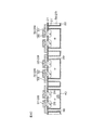
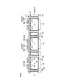
- FIG. 2 is a cross-sectional view of the LED package shown in FIG.
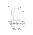
- FIG. 3 is a bottom view of the LED chip shown in FIG. 2 and a plan view of a diode chip.
- FIG. 3 is a cross-sectional view showing a part of the manufacturing process of the LED element unit shown in FIG. 2, showing a cut surface at the same position as in FIG. 2. It is a figure which shows the next process of FIG. 4A. It is a figure which shows the next process of FIG. 4B. It is a figure which shows the next process of FIG. 4C. It is a figure which shows the next process of FIG. 4D.
- FIG. 8 is a diagram showing a modification of the LED chip and the diode chip in FIG. 2, in which FIG. 8A is a plan view of the diode chip, and FIG.
- FIG. 8B is a bottom view of the LED chip.
- FIG. 9 is a bottom view of the diode chip of FIG. 8.
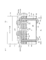
- FIG. 8 is a diagram showing a modification of the LED chip and the diode chip in FIG. 2, in which FIG. 8A is a plan view of the diode chip, and FIG. 8B is a bottom view of the LED chip. It is typical sectional drawing of the LED element unit which concerns on 2nd Embodiment of this invention.
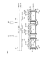
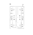
- FIG. 12A is a schematic view of an LED element unit according to a third embodiment of the present invention, FIG. 12A is a plan view of the whole, FIG. 12B is a plan view of an LED driver, and FIG. 12C is an LED chip. The bottom view of each is shown.
- FIG. 12A is a schematic view of an LED element unit according to a third embodiment of the present invention
- FIG. 12A is a plan view of the whole
- FIG. 12B is a plan view of an LED driver
- FIG. 12C is an LED
- FIG. 13 is a cross-sectional view of the LED element unit shown in FIG. 12A, showing a cross section taken along the line BB of FIG.
- FIG. 13 is a cross-sectional view of the LED element unit shown in FIG. 12A, showing a cross section taken along the line CC in FIG. It is a schematic block diagram of the LED lamp carrying an LED package.
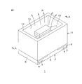
- FIG. 1 is a schematic perspective view of an LED package according to a first embodiment of the present invention.
- the LED package 1 is used for, for example, a traffic light, an electric bulletin board, a backlight of a liquid crystal display, various lights such as lamps for automobiles and bicycles, and a light source for photosensitive of an electrophotographic printer.
- the LED package 1 includes a base substrate 2 and a resin case 3 attached on the base substrate 2.
- the base substrate 2 is formed by fitting a metal cathode terminal 8 and an anode terminal 9 having recesses 6 and 7 to the protrusions 4 of the insulating substrate 5 having the protrusions 4 at the end portion. Are formed in a rectangular plate shape.
- Each of the cathode terminal 8 and the anode terminal 9 forms an end of the base substrate 2 in the longitudinal direction.
- the resin case 3 is formed in a wall shape that forms a square ring along the periphery of the base substrate 2 so as to surround the central portion of the base substrate 2.
- the four inner surfaces 10 (surfaces on the center portion side of the base substrate 2) of the wall-shaped resin case 3 are tapered surfaces in which a pair of surfaces facing each other spread from the surface of the base substrate 2 toward the top. .
- the inner surface 10 functions as a reflector (reflector).
- the LED element unit 11 as a light emitting element unit is mounted in the center part of the base substrate 2 surrounded by the resin case 3.
- the light generated in the LED element unit 11 is emitted from the open surface 12 (surface opposite to the base substrate 2) of the resin package.
- a translucent resin 66 may be injected into the portion surrounded by the resin case 3 so as to cover the LED element unit 11.
- the white resin 66A is injected into the lower part of the resin case 3 so as to cover the diode chip 15, and the wavelength conversion resin 66B is injected into the upper part of the resin case 3 so as to cover the LED chip 14. .
- the wavelength conversion resin 66B may have a lens shape, and the white resin 66A has a peripheral portion that is thicker than the central portion, for example, as shown by a dashed line in FIG. It may be formed to be curved. That is, the white resin 66A may have a relatively thin portion covering the diode chip 15 and a relatively thick contact portion with the resin case 3.
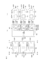
- FIG. 2 is a cross-sectional view of the LED package shown in FIG. 1, showing a cross section taken along the line AA of FIG.
- FIG. 3 is a bottom view of the LED chip shown in FIG. 2 and a plan view of the diode chip.
- An LED element unit 11 is provided at the center of the base substrate 2.
- the LED element unit 11 includes an LED chip 14 as a semiconductor light emitting element and a diode chip 15 as a support element that supports the LED chip 14.
- the LED chip 14 is obtained by forming a light emitting diode structure (LED layer 17) made of a group III nitride semiconductor layer on one main surface of a sapphire substrate 16 as a transparent substrate.
- An LED cathode electrode 19 as a first n-side electrode and an LED anode electrode 20 as a first p-side electrode are formed on the surface 18 of the LED layer 17.
- the LED cathode electrode 19 and the LED anode electrode 20 are formed in a bump shape made of Au, and are provided adjacent to each other.
- “n side” and “p side” are based on the cathode side (n side) and the anode side (p side) of the LED chip 14.
- the diode chip 15 includes a p-type silicon substrate 23 (for example, a p-type impurity concentration of about 1 ⁇ 10 19 cm ⁇ 3 ) as a conductive substrate having a front surface 21 and a back surface 22.
- An n + -type region 24 (for example, an n-type impurity concentration of about 1 ⁇ 10 20 cm ⁇ 3 ) is formed on the surface layer portion of the p-type silicon substrate 23 facing the LED chip 14 (surface 21). Yes.
- the n + -type region 24 is a region that is floating in the p-type silicon substrate 23 as, for example, a square island in plan view.
- an n + type region 24 and a p type region 25 excluding the n + type region 24 are formed on the p type silicon substrate 23, and a pn junction between the n + type region 24 and the p type region 25 is formed.
- a Zener diode structure is formed.
- a Zener diode having such a structure has a Zener voltage determined by the concentration relationship between the n + -type region 24 and the p-type region 25.
- Zener breakdown occurs at the interface between the n + -type region 24 and the p-type region 25. That is, the diode chip 15 functions as a protection element for the LED chip 14. Therefore, the LED chip 14 and the diode chip 15 constitute a light emitting element circuit having a protection circuit in cooperation with each other.
- a p + -type contact region 26 having a higher p-type impurity concentration than the p-type region 25 (for example, the p-type impurity concentration is about 1 ⁇ 10 20 cm ⁇ 3 ) is formed on the surface layer portion of the p-type silicon substrate 23. Is formed. Similar to the n + type region 24, the p + type contact region 26 is, for example, a floating region as a square island in plan view, and is formed adjacent to the n + type region 24.
- a surface protective film 27 made of SiO 2 is formed on the surface 21 of the p-type silicon substrate 23.
- a diode anode electrode 28 as a second n-side electrode and a diode cathode electrode 29 as a second p-side electrode are formed on the surface protective film 27.
- the diode anode electrode 28 includes an n-side wiring 30 made of Al and an n-side bump 31 made of Au.
- the n-side wiring 30 is located immediately above the p + -type contact region 26, passes through the surface protective film 27 and is connected to the p + -type contact region 26, and the n-side contact in plan view
- An n-side extraction portion 33 that is extracted from the portion 32 to the opposite side of the n + -type region 24 is integrally provided.
- the n-side lead portion 33 made of Al functions as a relay wiring that connects the p + -type contact region 26 and the n-side via 41 (described later), and also functions as a light reflector on the surface of the diode chip 15. Therefore, as the area of the n-side extraction portion 33 is increased, the light reflection area is increased, so that the light reflectance can be improved.
- an insulating film may be provided on the side surface of the diode chip 15, and a reflective film may be further formed to further improve the reflectance.
- the n-side bump 31 is bonded onto the n-side contact portion 32 of the n-side wiring 30 and is disposed immediately above the p + -type contact region 26.
- the diode cathode electrode 29 includes a p-side wiring 34 made of Al and a p-side bump 35 made of Au.
- the p-side wiring 34 is located immediately above the n + -type region 24, and passes through the surface protective film 27 and connected to the n + -type region 24, and the p-side contact portion 36 in plan view. And a p-side lead portion 37 that is drawn to the opposite side of the p + -type contact region 26.
- the p-side lead portion 37 made of Al functions as a relay wiring that connects the n + -type region 24 and the p-side via 42 (described later), and also functions as a light reflector on the surface of the diode chip 15. Therefore, since the light reflection area increases as the area of the p-side lead-out portion 37 is increased, the light reflectance can be improved.
- the p-side bump 35 is bonded onto the p-side contact portion 36 of the p-side wiring 34 and is disposed immediately above the n + -type region 24.
- An n-side via hole 38 and a p-side via hole 39 are formed in the p-type silicon substrate 23 so as to penetrate the surface protective film 27 from the back surface 22 and reach the n-side wiring 30 and the p-side wiring 34, respectively.
- the n-side via hole 38 and the p-side via hole 39 are formed in a square shape in plan view.
- n-side via holes 38 through the side of the p + -type contact region 26 so as not to contact the p + -type contact region 26 is disposed at a position overlapping the n-side lead-out portion 33 in a plan view.
- p-side via holes 39 through the side of the n + -type region 24 so as not to contact the n + -type region 24 is disposed at a position overlapping the p-side lead section 37 in a plan view.
- the n-side via hole 38 and the p-side via hole 39 are arranged on the same straight line (dashed line L in FIG. 3) together with the n + -type region 24 and the p + -type contact region 26 so as not to overlap in plan view. Has been.
- a fixed interval is provided between the n-side via hole 38 and the p + -type contact region 26 and between the p-side via hole 39 and the n + -type region 24.
- An insulating film 40 made of SiO 2 is integrally formed on the inner surfaces of the n-side via hole 38 and the p-side via hole 39 and on the back surface 22 of the p-type silicon substrate 23. Then, an n-side via 41 and a p-side via 42 made of Cu are formed so as to fill the inside of the insulating film 40 in the n-side via hole 38 and the p-side via hole 39.
- the n-side via 41 is connected to the n-side lead portion 33, and the p-side via 42 is connected to the p-side lead portion 37. Further, the n-side via 41 and the p-side via 42 may be tapered vias whose diameter gradually decreases in the direction from the front surface 21 to the back surface 22 of the p-type silicon substrate 23.
- An n-side island 43 drawn from the n-side via 41 along the back surface 22 of the p-type silicon substrate 23 is formed on the insulating film 40 on the back surface 22 of the p-type silicon substrate 23. It is integrally formed.
- An n-side external bump 44 made of solder as an n-side external electrode is joined to the n-side island 43.
- a p-side island 45 drawn from the p-side via 42 along the back surface 22 of the p-type silicon substrate 23 is formed on the insulating film 40 on the back surface 22 of the p-type silicon substrate 23. It is integrally formed.
- a p-side external bump 46 made of solder as a p-side external electrode is joined to the p-side island 45.
- the bump-shaped LED cathode electrode 19 and the n-side bump 31 (diode anode electrode 28), and the bump-shaped LED anode electrode 20 and the p-side bump 35 (diode cathode electrode 29) are joined.
- the LED chip 17 is supported from below by the diode chip 15 in a face-down posture with the surface 18 of the LED layer 17 facing downward.
- the LED element unit 11 having a stack structure of the LED chip 14 and the diode chip 15 is configured.
- the LED cathode electrode 19 and the LED anode electrode 20 of the LED layer 17, and the n + type region 24 and the p type region 25 of the Zener diode with respect to the n side external bump 44 and the p side external bump 46. are connected in parallel.
- the n-side external bump 44 of the diode chip 15 is connected to the portion of the cathode terminal 8 that protrudes toward the center of the base substrate 2 with respect to the resin case 3, and the p-side external bump 46 is the anode.
- the terminal 9 is disposed at the center of the base substrate 2 by being connected to a portion of the terminal 9 that protrudes toward the center of the base substrate 2 with respect to the resin case 3.
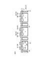
- FIG. 4A to 4I are cross-sectional views showing a part of the manufacturing process of the LED element unit shown in FIG. 2 in the order of steps, and showing a cut surface at the same position as FIG.
- the LED element unit 11 is manufactured in the state of the wafer 56 before the p-type silicon substrate 23 is cut into individual pieces.
- an n + -type region 24 and a p + -type contact region 26 are formed in the surface layer portion of the p-type silicon substrate 23 by a known ion implantation technique.
- a surface protective film 27 made of SiO 2 is formed on the surface 21 of the p-type silicon substrate 23 by thermal oxidation.
- the surface protective film 27 is patterned by a known patterning technique, and an opening exposing the n + -type region 24 and the p + -type contact region 26 is formed in the surface protective film 27.
- an Al layer is deposited over the entire surface of the surface protective film 27 by sputtering.
- the deposited Al layer is patterned by a known patterning technique, whereby the n-side wiring 30 and the p-side wiring 34 having a predetermined pattern are formed.
- n-side bumps 31 and p-side bumps 35 made of Au are formed on the n-side wiring 30 and the p-side wiring 34.
- the p-type silicon substrate 23 is ground and thinned from the back surface 22 side.
- a p-type silicon substrate 23 having a thickness of 700 ⁇ m is thinned to about 130 ⁇ m.
- an insulating film 40 made of SiO 2 is formed on the inner surfaces of the n-side via hole 38 and the p-side via hole 39 and the back surface 22 of the p-type silicon substrate 23 by a CVD (Chemical Vapor Deposition) method. It is formed.
- the portions on the n-side wiring 30 and the p-side wiring 34 in the insulating film 40 are selectively removed by etching.
- a barrier film (not shown) made of Ti is formed on the insulating film 40, and a seed film (not shown) made of Cu is formed on the barrier film by sputtering.
- a resist 13 having openings in portions where the n-side island 43 and the p-side island 45 are to be formed is formed on the Cu seed film and the Ti barrier film.
- Cu is plated and grown on the n-side via hole 38 and the p-side via hole 39 and on the back surface 22 of the p-type silicon substrate 23 from the Cu seed film exposed from the opening of the resist 13.
- the n-side via 41, the p-side via 42, the n-side island 43, and the p-side island 45 are formed simultaneously.
- the resist 13 is stripped, and the excess Cu seed film exposed in the portion where the resist 13 was formed is removed. Subsequently, an n-side external bump 44 and a p-side external bump 46 made of solder are formed on the n-side island 43 and the p-side island 45.
- the dicing blade 57 is advanced from the sapphire substrate 16 to the LED wafer 59 in which the LED layer 17 is formed on the sapphire substrate 16 in the state of the wafer 58, whereby each LED The LED chip 14 is cut on a dicing line set along the periphery of the chip 14. As a result, the wafer 58 is separated into individual LED chips 14.
- the LED cathode electrode 19 and the LED anode electrode 20 of each LED chip 14 separated into pieces are bonded to the n-side bump 31 and the p-side bump 35 on a one-to-one basis.
- the dicing blade 60 is advanced from the back surface 22 side of the p-type silicon substrate 23, as shown in FIG. 4I, the p-type silicon substrate is placed on the dicing line set along the periphery of each diode chip 15. 23 is cut off. Thereby, the LED element unit 11 having a stack structure of the LED chip 14 and the diode chip 15 is obtained.
- the LED chip 14 is bonded to the diode chip 15 in a so-called face-down posture with the electrode formation surface (surface 18) of the LED layer 17 facing downward.
- the LED element unit 11 can be downsized (shrinked).
- the diode anode electrode 28 and the diode cathode electrode 29 joined to the LED cathode electrode 19 and the LED anode electrode 20 of the LED chip 14 respectively pass through the p-type silicon substrate 23 in the thickness direction, and the n-side via 41 and the p-side.
- the vias 42 are connected to the n-side external bump 44 and the p-side external bump 46, respectively.
- the n-side via 41 and the p-side via 42 are insulated from the p-type silicon substrate 23 by covering the side surfaces with the insulating film 40.
- Each of the n-side wiring 30 and the p-side wiring 34 has a lead portion (n-side lead portion 33 and p-side lead portion 37), and the lead-out portions 33 and 37 have an n-side via 41 and a p-side via. 42 is connected.
- veer 42 can be expanded by changing the pattern of the drawer
- the n-side via 41 and the p-side via 42 can be provided so as not to contact the n + -type region 24 and the p + -type contact region 26. Therefore, even in the downsized LED element unit 11, the n + type region 24 and the p + type contact region 26 are not inhibited. As a result, the Zener diode formed on the p-type silicon substrate 23 can sufficiently exhibit the function of protecting the LED chip 14 from overcurrent.
- thermo conductivity is about 320 W / (m ⁇ K)
- Al thermal conductivity is about 236 W / (m ⁇ K).
- thermo conductivity is about 398 W / (m ⁇ K)
- thicker n-side via 41 and p-side via 42 than the bonding wire Since it can be dissipated to the base substrate 2 through the n-side external bump 44 and the p-side external bump 46 made of solder (thermal conductivity is about 70 to 80 W / (m ⁇ K)), heat dissipation is improved. be able to.
- the diode anode electrode 28 and the diode cathode electrode 29 are connected to the cathode terminal 8 and the anode terminal 9 of the base substrate 2 by using bonding wires. There is a possibility that the bonding wire may be disconnected due to a difference in thermal expansion coefficient of the bonding wire.
- the diode anode electrode 28 and the diode cathode electrode 29 are connected to the cathode terminal 8 and the anode terminal 9 of the base substrate 2, respectively,
- the p-side external bumps 46 are used for connection. Thereby, it is possible to reduce the occurrence of connection failure due to disconnection or the like of the bonding wire.
- the diode chip 15 may be a thin chip as shown in FIG.
- the thickness of the diode chip 15 can be set to 50 ⁇ m to 100 ⁇ m, for example, and the lengths of the n-side via 41 and the p-side via 42 in the thickness direction can be shortened. It is possible to improve the thermal conductivity in the direction of travel.
- the cathode terminal 8 and the anode terminal 9 may be lead terminals formed in a rectangular plate shape as shown in FIG. In this case, since the n-side external bump 44 and the p-side external bump 46 are directly connected to the lead terminals, the thermal conductivity of the LED package 1 can be improved.
- the n-side via 41 and the p-side via 42 are formed as large as possible, and even if a plurality of the n-side via 41 and the p-side via 42 are formed in the diode chip 15 as shown in FIG. 7. Good. Thereby, the thermal conductivity in the direction from the front surface to the back surface of the diode chip 15 can be improved.
- the diode chip 15 may be provided so as to be connected to the plurality of LED chips 14. In this case, one n-side wiring 30 and one p-type wiring 34 may be provided for each LED chip 14 as shown in FIG.
- the n-side island 43 and the p-side island 45 collectively connect the n-side via 41 and the p-side via 42 connected to each n-side wiring 30 and each p-side wiring 34 as shown in FIG. It may be provided so that it may be provided, or one n-side via 41 and one p-side via 42 may be provided. Further, the n-side wiring 30 and the p-type wiring 34 may be provided as a common wiring for all the LED chips 14 as shown in FIG. In this case, one n-side bump 31 and one p-side bump 35 may be provided for each LED chip 14. Moreover, when using more LED chips 14, you may make it use multilayer wiring. Second Embodiment FIG.
- FIG. 11 is a schematic cross-sectional view of an LED element unit according to the second embodiment of the present invention.
- parts corresponding to the parts shown in FIG. 2 are given the same reference numerals as those parts. Further, in the following, detailed description of the parts denoted by the same reference numerals is omitted.
- a first interlayer insulating film 62 and a second interlayer insulating film 63 made of SiO 2 are sequentially stacked on the surface protective film 27.
- the n-side wiring 30 and the p-side wiring 34 penetrate the second interlayer insulating film 63, the first interlayer insulating film 62, and the surface protective film 27 from the surface of the second interlayer insulating film 63, and pass through the n + -type region 24 and p. Each is connected to a + type contact region 26.
- the n-side lead portion 33 of the n-side wiring 30 is divided along a direction crossing the lead-out direction.
- a resistance element 64 made of polysilicon is formed so as to straddle between the divided n-side lead portions 33.
- the resistance element 64 is connected to each divided n-side lead portion 33 by a plug 65. Thereby, the resistance element 64 is connected in series between the connection position of the n-side via 41 in the n-side wiring 30 and the connection position of the n-side bump 31 (position of the n-side contact portion 32).
- the same operational effects as those of the LED element unit 61 of the first embodiment can be exhibited. Furthermore, in the LED element unit 61, since the resistance element 64 is connected in series to the n-side wiring 30, by appropriately setting the resistance value of the resistance element 64, the current flowing through the LED chip 14 is changed to the LED element. It is possible to satisfactorily control the rated current of the chip 14.
- FIG. 12A and 12B are schematic views of an LED element unit according to the third embodiment of the present invention, in which FIG. 12A is a plan view of the whole, FIG. 12B is a plan view of an LED driver, and FIG. ) Shows bottom views of the LED chips.
- 13 is a cross-sectional view of the LED element unit shown in FIG. 12 (a), showing a cross section taken along the line BB of FIG. 12 (a).
- FIG. 14 is a cross-sectional view of the LED element unit shown in FIG. 12 (a), showing a cross section taken along the line CC of FIG.
- FIG. 13 and FIG. 14 portions corresponding to the respective portions shown in FIG. 2 and FIG. 3 are given the same reference numerals as those portions. Further, in the following, detailed description of the parts denoted by the same reference numerals is omitted.
- the LED element unit 81 of the third embodiment includes a plurality of LED chips 82R, 82G, and 82B and an LED driver 83 as a drive element that collectively supports the plurality of LED chips 82R, 82G, and 82B. .
- the plurality of LED chips 82R, 82G, and 82B have different emission wavelengths, the red LED chip 82R (emission wavelength is 615 nm to 665 nm), the green LED chip 82G (emission wavelength is 515 nm to 540 nm), and the blue LED chip 82B (emission wavelength). Is 445 nm to 480 nm).
- the green LED chip 82 ⁇ / b> G has a SiC substrate 47 instead of the sapphire substrate 16, and the LED layer 17 is formed on one main surface of the SiC substrate 47.
- the red LED chip 82 ⁇ / b> R has a GaAs substrate 48 instead of the sapphire substrate 16, and the LED layer 17 is formed on one main surface of the GaAs substrate 48.
- the LED driver 83 includes a silicon substrate 85 on which a driving IC 84 (driving circuit) for driving the individual LED chips 82R, 82G, and 82B is formed.
- a surface protective film 90 made of SiO 2 is formed on the surface 86 of the silicon substrate 85.
- a cathode electrode 88 as a second n-side electrode and anode electrodes 89R, 89G, and 89B as second p-side electrodes are formed adjacent to each other.
- the cathode electrode 88 is a common electrode for the three LED chips 82R, 82G, and 82B.
- a total of three pairs of anode electrodes 89R, 89G, and 89B are provided for each of the LED chips 82R, 82G, and 82B.
- the anode electrodes 89R, 89G, and 89B include anode wirings 94R, 94G, and 94B and anode bumps 95R, 95G, and 95B, which are provided for each of the LED chips 82R, 82G, and 82B.
- Each of the anode wirings 94R, 94G, and 94B is opposite to the cathode electrode 88 from the anode contact portions 96R, 96G, and 96B with which the anode bumps 95R, 95G, and 95B are contacted, and the anode contact portions 96R, 96G, and 96B in plan view.
- An anode lead portion 97R, 97G, 97B drawn to the side is integrally provided.
- the silicon substrate 85 is formed with cathode via holes 98 and anode via holes 99R, 99G, and 99B that penetrate the surface protective film 90 from the back surface 87 and reach the cathode electrode 88 and the anode wirings 94R, 94G, and 94B, respectively.
- the cathode via hole 98 and the anode via holes 99R, 99G, and 99B are formed, for example, in a square shape in plan view.
- One cathode via hole 98 is provided for the common cathode electrode 88.
- a total of three anode via holes 99R, 99G, 99B are provided for each LED chip 82R, 82G, 82B.
- anode via holes 99R, 99G, and 99B are arranged at positions overlapping the anode lead portions 97R, 97G, and 97B in a plan view.
- An insulating film 100 made of SiO 2 is integrally formed on the inner surfaces of the cathode via hole 98 and the anode via holes 99R, 99G, and 99B and the back surface 87 of the silicon substrate 85.
- the cathode via 101 and the anode vias 102R, 102G, 102B made of Cu are formed so as to fill the inside of the insulating film 100 in the cathode via hole 98 and the anode via holes 99R, 99G, 99B.
- the cathode via 101 is connected to the cathode electrode 88, and the anode vias 102R, 102G, and 102B are connected to the anode lead portions 97R, 97G, and 97B.
- a cathode island 103 drawn from the cathode via 101 along the back surface 87 of the silicon substrate 85 is formed integrally with the cathode via 101 on the portion of the insulating film 100 on the back surface 87 of the silicon substrate 85.
- the cathode island 103 is joined with cathode external bumps 104 made of solder as cathode external electrodes.
- anode islands 105R, 105G, and 105B drawn along the back surface 87 of the silicon substrate 85 from the anode vias 102R, 102G, and 102B are formed on the insulating film 100 on the back surface 87 of the silicon substrate 85. , 102B.
- Anode external bumps 106R, 106G, and 106B made of solder as anode external electrodes are joined to the anode islands 105R, 105G, and 105B.
- the red LED chip 82R, the green LED chip 82G, and the blue LED chip 82B are bonded to the bump-shaped LED cathode electrode 19 and the cathode electrode 88, and the bump-shaped LED anode electrode 20 and the anode bumps 95R, 95G, and 95B, respectively.
- the LED driver 83 is supported from below in a face-down posture with the surface 18 of the LED layer 17 facing downward (FIGS. 12A and 13).
- the plurality of LED chips (the red LED chip 82R, the green LED chip 82G, and the blue LED chip 82B) are disposed below the electrode formation surface (surface 18) of the LED layer 17.
- the LED driver 83 is joined in a so-called face-down posture.
- the LED chips 82R, 82G, and 82B and the LED driver 83 can be stacked, so that the LED element unit 81 can be downsized (shrinked).
- a cathode via 101 in which the cathode electrode 88 and the anode electrodes 89R, 89G, and 89B joined to the LED cathode electrode 19 and the LED anode electrode 20 of each LED chip 82R, 82G, and 82B penetrate the silicon substrate 85 in the thickness direction.
- the anode external bumps 104 and the anode external bumps 106R, 106G, and 106B are connected to each other by the anode vias 102R, 102G, and 102B, respectively.
- the cathode via 101 and the anode vias 102R, 102G, and 102B are insulated from the silicon substrate 85 by covering the side surfaces with the insulating film 100. Therefore, when power is supplied from the cathode external bump 104 and the anode external bumps 106R, 106G, 106B to the LED chips 82R, 82G, 82B via the vias (cathode via 101 and anode vias 102R, 102G, 102B), the vias (cathode via 101 and The anode vias 102R, 102G, and 102B) and the silicon substrate 85 can be prevented from being short-circuited. As a result, power can be normally supplied to the LED chips 82R, 82G, and 82B.
- the elements stacked with the LED chip are not limited to the elements (diode chip 15 and LED driver 83) exemplified in the first to third embodiments, but may be variable resistance elements.
- the insulating films 40 and 100 covering the side surfaces of the vias are not limited to SiO 2 but may be SiN or the like.
- vias (n-side via 41 and p-side via 42) penetrating the p-type silicon substrate 23 are provided on both the cathode side (n side) and the anode side (p side). Although formed, one can be omitted.
- a configuration in which the conductivity type of each semiconductor region is reversed may be employed. That is, in the diode chip 15, a configuration in which the n-type (first conductivity type) region is a p-type (second conductivity type) region and the p-type region is an n-type region is employed. Good. Also, wiring connecting the second n-side electrode 28 and the n-side external bump 44, wiring connecting the second p-side electrode 29 and the p-side external bump 46, wiring connecting the cathode electrode 88 and the cathode external bump 104, etc. May not be vias penetrating the silicon substrates 23 and 85, respectively. For example, in the diode chip 15 of the LED element unit 11 of the first embodiment, the wiring formed along the side surface of the silicon substrate 23 may be used.
- the LED element unit 11 uses the n-side external bump 44 and the p-side external bump 46 as leads of the lead frame, respectively. May be directly mounted on the lead frame without the base substrate 2 or the like.
- the LED chips 14, 82R, 82G, and 82B illustrated in the first to third embodiments are schematic, and the LED chips 14, 82R, 82G, and 82B are LEDs having a general structure. An element can be used.
- Examples of application products of the LED package 1 or the LED element units 11, 61, 71, 81 in the first to third embodiments are, for example, an LED lamp, a backlight, a 7-segment display, and a dot matrix display. Etc.
- an LED lamp As an example of the configuration of the LED lamp, as shown in FIG. 15, a configuration in which a plurality of LED packages 1 are installed on a substrate 67 (R is a resistor and C is a capacitor) can be mentioned.
- the LED element units 11, 61, 71, 81 alone may be installed instead of the LED package 1.
- Diode cathode electrode 30 ... n-side wiring, 31 ... n-side bump, 34 ... p-side wiring, 35 ... p-side bump, 40. ..Insulating film, 41 ... n-side via, 4 ... p-side vias, 44 ... n-side external bumps, 46 ... p-side external bumps, 61 ... LED element unit, 64 ... resistive element, 81 ... LED element unit, 82R ..Red LED chip, 82G ... Green LED chip, 82B ... Blue LED chip, 83 ... LED driver, 84 ... Drive IC, 85 ... Silicon substrate, 86 ... (Silicon substrate) ) Front surface, 87...
Landscapes
- Engineering & Computer Science (AREA)
- Physics & Mathematics (AREA)
- Microelectronics & Electronic Packaging (AREA)
- Optics & Photonics (AREA)
- General Engineering & Computer Science (AREA)
- Led Device Packages (AREA)
- Power Engineering (AREA)
Abstract
Description
一方、発光素子およびツェナーダイオードをスタック構造にできれば、絶縁基板上のスペースが素子1つ分で済むので、装置全体としての小型化(シュリンク化)を図ることができるかもしれない。
本発明の目的は、半導体発光素子および支持素子のスタック構造により小型化を図ることができ、さらに、半導体発光素子に対して電力を正常に供給できる発光素子ユニットおよび当該発光素子ユニットを備える発光素子パッケージを提供することである。
さらに、半導体発光素子の第1n側電極および第1p側電極それぞれに接合された第2n側電極および第2p側電極のうち少なくとも一方は、支持素子の導電性基板を厚さ方向に貫通するビアによって外部電極(n側外部電極、p側外部電極)に電気的に接続されている。そして、第2n側電極および/または第2p側電極と外部電極とを導通させるビアは、その側面が絶縁膜で覆われることによって、導電性基板に対して絶縁されている。そのため、外部電極からビアを介して半導体発光素子に電力を供給する際、ビアと導電性基板とが短絡することを防止することができる。その結果、半導体発光素子に対して電力を正常に供給することができる。
この構成によれば、導電性基板とビアとが配線によって接続されているので、配線のパターンを適宜変更することにより、ビアの形成位置の自由度を広げることができる。これにより、導電性基板において、ダイオード等が形成される素子形成領域と、ビアが形成されるビア形成領域とを分離することができる。その結果、小型化された発光素子ユニットにおいても、素子形成領域を阻害せずに、導電性基板を貫通するビアを形成することができる。
この構成によれば、抵抗素子が半導体発光素子に対して直列に接続されているので、当該抵抗素子の抵抗値を適切に設定することにより、半導体発光素子に流れる電流を、当該発光素子の定格電流に良好に制御することができる。
また、本発明の発光素子ユニットでは、前記配線は、Alからなっていてもよい。
本発明の発光素子ユニットでは、前記導電性基板が、前記第2n側電極が接続されたp型領域と、前記第2p側電極が接続されたn型領域とを有し、前記支持素子が、当該n型領域と当該p型領域とのpn接合を有するツェナーダイオードを含む場合、前記ビアは、前記第2n側電極および前記第2p側電極それぞれに接続されたn側ビアおよびp側ビアを含むことが好ましい。
たとえば、前記導電性基板が、前記p型領域としてのp型半導体基板であり、前記n型領域が、当該p型半導体基板の表層部にフローティングされた領域である場合、前記p側ビアは、フローティングされた前記n型領域に接触しないように前記p型半導体基板を貫通していることが好ましい。
また、前記p型半導体基板が、その表層部において前記n型領域に隣接して形成され、前記第2n側電極が接続されたp+型コンタクト領域を含む場合、前記p側ビアは、前記n型領域に対して前記p+型コンタクト領域とは反対側に形成されており、前記n側ビアは、前記p+型コンタクト領域に対して前記n型領域とは反対側に形成されていることが好ましい。具体的には、前記n側ビア、前記n型領域、前記p+型コンタクト領域および前記p側ビアが、平面視において同一直線上に配置されていてもよい。
この構成によれば、1つの駆動素子に対して複数の半導体発光素子をスタック構造できるので、構造の小型化(シュリンク化)を図ることができる。
<第1実施形態>
図1は、本発明の第1実施形態に係るLEDパッケージの模式的な斜視図である。
LEDパッケージ1は、たとえば、信号機、電光掲示板、液晶ディスプレイのバックライト、自動車および自転車のランプ等の各種照明、電子写真式プリンタの感光用光源などに用いられる。
ベース基板2は、端部に凸条4を有する絶縁性基板5の凸条4に対して、凹条6,7を有する金属製のカソード端子8およびアノード端子9を嵌合させることにより、全体として長方形板状に形成したものである。カソード端子8およびアノード端子9はそれぞれ、ベース基板2の長手方向の各端部を形成している。
ベース基板2の中央部には、LED素子ユニット11が設けられている。
LED素子ユニット11は、半導体発光素子としてのLEDチップ14と、当該LEDチップ14を支持する支持素子としてのダイオードチップ15とを備えている。
LED層17の表面18には、第1n側電極としてのLEDカソード電極19および第1p側電極としてのLEDアノード電極20が形成されている。LEDカソード電極19およびLEDアノード電極20は、Auからなるバンプ状に形成されており、互いに隣接して設けられている。なお、以下で説明において、「n側」および「p側」とは、LEDチップ14のカソード側(n側)およびアノード側(p側)を基準としている。
ダイオードチップ15は、表面21および裏面22を有する導電性基板としてのp型シリコン基板23(たとえば、p型不純物濃度が1×1019cm-3程度)を備えている
。p型シリコン基板23におけるLEDチップ14との対向面(表面21)側の表層部には、n+型領域24(たとえば、n型不純物濃度が1×1020cm-3程度)が形成されている。n+型領域24は、p型シリコン基板23において、たとえば、平面視四角状の島としてフローティングされた領域である。
表面保護膜27上には、第2n側電極としてのダイオードアノード電極28および第2p側電極としてのダイオードカソード電極29が形成されている。
ダイオードアノード電極28は、Alからなるn側配線30と、Auからなるn側バンプ31とを備えている。
ダイオードカソード電極29は、Alからなるp側配線34と、Auからなるp側バンプ35とを備えている。
p側配線34は、n+型領域24の直上に位置し、表面保護膜27を貫通してn+型領域24に接続されたp側コンタクト部36と、平面視において当該p側コンタクト部36からp+型コンタクト領域26とは反対側に引き出されたp側引出し部37とを一体的に有している。Alからなるp側引出し部37は、n+型領域24とp側ビア42(後述)とを接続する中継配線として機能するとともに、ダイオードチップ15の表面上において光の反射板として機能する。したがって、p側引出し部37の面積を大きくするほど光の反射面積が大きくなるので、光の反射率を向上させることができる。
p型シリコン基板23には、その裏面22から表面保護膜27を貫通し、n側配線30およびp側配線34それぞれに達するn側ビアホール38およびp側ビアホール39が形成されている。n側ビアホール38およびp側ビアホール39は、たとえば、平面視四角状に形成されている。
n側ビアホール38およびp側ビアホール39の内面ならびにp型シリコン基板23の裏面22には、SiO2からなる絶縁膜40が一体的に形成されている。
そして、n側ビアホール38およびp側ビアホール39における絶縁膜40の内側を埋め尽くすように、Cuからなるn側ビア41およびp側ビア42が形成されている。n側ビア41はn側引出し部33に接続され、p側ビア42はp側引出し部37に接続されることとなる。また、n側ビア41およびp側ビア42は、p型シリコン基板23の表面21から裏面22へ向かう方向に径が徐々に小さくなるテーパービアであってもよい。
また、絶縁膜40におけるp型シリコン基板23の裏面22上の部分には、p側ビア42からp型シリコン基板23の裏面22に沿って引き出されたp側アイランド45が、p側ビア42と一体的に形成されている。このp側アイランド45には、p側外部電極としての半田からなるp側外部バンプ46が接合されている。
図4A~図4Iは、図2に示すLED素子ユニットの製造工程の一部を工程順に示す断面図であって、図2と同じ位置での切断面を示す。
次に、図4Dに示すように、エッチングにより、当該絶縁膜40におけるn側配線30およびp側配線34上の部分が選択的に除去される。
次に、図4Gに示すように、ウエハ58の状態のサファイア基板16上にLED層17が形成されたLEDウエハ59に対して、サファイア基板16からダイシングブレード57が進出されることにより、各LEDチップ14の周縁に沿って設定されたダイシングライン上でLEDチップ14が切断される。これにより、ウエハ58が各LEDチップ14に個片化される。
次に、p型シリコン基板23の裏面22側からダイシングブレード60が進出されることにより、図4Iに示すように、各ダイオードチップ15の周縁に沿って設定されたダイシングライン上でp型シリコン基板23が切断される。これにより、LEDチップ14およびダイオードチップ15のスタック構造を有するLED素子ユニット11が得られる。
そして、n側ビア41およびp側ビア42は、その側面が絶縁膜40で覆われることによって、p型シリコン基板23に対して絶縁されている。そのため、n側外部バンプ44およびp側外部バンプ46からビア(n側ビア41およびp側ビア42)を介してLEDチップ14に電力を供給する際、ビア(n側ビア41およびp側ビア42)とp型シリコン基板23とが短絡することを防止することができる。その結果、LEDチップ14に対して電力を正常に供給することができる。
また、LEDパッケージ1において、カソード端子8およびアノード端子9は、図6に示すように、それ自体が長方形板状に形成されたリード端子であってもよい。この場合、n側外部バンプ44およびp側外部バンプ46が直接リード端子に接続されることとなるので、LEDパッケージ1の熱伝導性を向上させることができる。
また、LED素子ユニット11では、ダイオードチップ15は、複数のLEDチップ14に接続されるように設けられていてもよい。この場合、n側配線30およびp型配線34は、図8に示すように、各LEDチップ14に対して1つずつ設けられていてもよい。この場合、n側アイランド43およびp側アイランド45は、図9に示すように、各n側配線30および各p側配線34に接続されたn側ビア41およびp側ビア42を一括して接続するように設けられていてもよいし、各n側ビア41および各p側ビア42に対して1つずつ設けられていてもよい。また、n側配線30およびp型配線34は、図10に示すように、全てのLEDチップ14の共通の配線として設けられていてもよい。この場合、n側バンプ31およびp側バンプ35は、各LEDチップ14に対して1つずつ設けられていてもよい。また、より多くのLEDチップ14を用いる場合には、多層配線を用いるようにしてもよい。
<第2実施形態>
図11は、本発明の第2実施形態に係るLED素子ユニットの模式的な断面図である。なお、図11において、前述の図2に示す各部に対応する部分には、それらの各部と同一の参照符号を付している。また、以下では、同一の参照符号を付した部分についての詳細な説明を省略する。
n側配線30およびp側配線34は、第2層間絶縁膜63の表面から第2層間絶縁膜63、第1層間絶縁膜62および表面保護膜27を貫通して、n+型領域24およびp+型コンタクト領域26にそれぞれ接続されている。
抵抗素子64は、分断された各n側引出し部33に対して、プラグ65により接続されている。これにより、抵抗素子64は、n側配線30におけるn側ビア41の接続位置とn側バンプ31の接続位置(n側コンタクト部32の位置)との間に直列に接続されることになる。
さらに、LED素子ユニット61では、抵抗素子64がn側配線30に直列に接続されているので、当該抵抗素子64の抵抗値を適切に設定することにより、LEDチップ14に流れる電流を、当該LEDチップ14の定格電流に良好に制御することができる。
<第3実施形態>
図12は、本発明の第3実施形態に係るLED素子ユニットの模式図であって、図12(a)が全体の平面図、図12(b)がLEDドライバの平面図、図12(c)がLEDチップの底面図をそれぞれ示す。図13は、図12(a)に示すLED素子ユニットの断面図であって、図12(a)のB-B切断面における断面を示す。図14は、図12(a)に示すLED素子ユニットの断面図であって、図12(a)のC-C切断面における断面を示す。なお、図12(a)~(c)、図13および図14において、前述の図2および図3に示す各部に対応する部分には、それらの各部と同一の参照符号を付している。また、以下では、同一の参照符号を付した部分についての詳細な説明を省略する。
複数のLEDチップ82R,82G,82Bは、互いに発光波長が異なる、赤色LEDチップ82R(発光波長が615nm~665nm)、緑色LEDチップ82G(発光波長が515nm~540nm)および青色LEDチップ82B(発光波長が445nm~480nm)である。なお、緑色LEDチップ82Gは、サファイア基板16に代えて、SiC基板47を有しており、このSiC基板47の一主面にLED層17を形成したものである。また、赤色LEDチップ82Rは、サファイア基板16に代えて、GaAs基板48を有しており、このGaAs基板48の一主面にLED層17を形成したものである。
表面保護膜90上には、第2n側電極としてのカソード電極88および第2p側電極としてのアノード電極89R,89G,89Bが互いに隣接して形成されている。カソード電極88は、3つのLEDチップ82R,82G,82Bに対して共通の電極となっている。一方、アノード電極89R,89G,89Bは、各LEDチップ82R,82G,82Bに対して一つずつ合計3対設けられている。
各アノード配線94R,94G,94Bは、アノードバンプ95R,95G,95Bがコンタクトされるアノードコンタクト部96R,96G,96Bと、平面視において当該アノードコンタクト部96R,96G,96Bからカソード電極88とは反対側に引き出されたアノード引出し部97R,97G,97Bとを一体的に有している。
カソードビアホール98およびアノードビアホール99R,99G,99Bの内面ならびにシリコン基板85の裏面87には、SiO2からなる絶縁膜100が一体的に形成されている。
また、絶縁膜100におけるシリコン基板85の裏面87上の部分には、アノードビア102R,102G,102Bからシリコン基板85の裏面87に沿って引き出されたアノードアイランド105R,105G,105Bが、アノードビア102R,102G,102Bと一体的に形成されている。このアノードアイランド105R,105G,105Bには、アノード外部電極としての半田からなるアノード外部バンプ106R,106G,106Bが接合されている。
たとえば、LEDチップとともにスタック構造される素子としては、前述の第1~第3実施形態に例示した素子(ダイオードチップ15、LEDドライバ83)に限らず、可変抵抗素子などであってもよい。
また、前述の第1および第2実施形態では、カソード側(n側)およびアノード側(p側)の両方にp型シリコン基板23を貫通するビア(n側ビア41およびp側ビア42)を形成したが、一方を省略することもできる。
また、第2n側電極28とn側外部バンプ44とを接続する配線、第2p側電極29とp側外部バンプ46とを接続する配線、カソード電極88とカソード外部バンプ104とを接続する配線等は、それぞれシリコン基板23,85を貫通するビアでなくてもよい。たとえば、第1実施形態のLED素子ユニット11のダイオードチップ15において、シリコン基板23の側面に沿って形成された配線等であってもよい。
また、第1~第3実施形態で図示されたLEDチップ14,82R,82G,82Bは模式的なものであり、これらのLEDチップ14,82R,82G,82Bとしては、一般的な構造のLED素子を用いることができる。
また、本発明の各実施形態において表した構成要素は、本発明の範囲で組み合わせることができる。
Claims (37)
- 表面および裏面を有し、当該裏面から光が取り出され、当該表面に第1n側電極および第1p側電極を有する半導体発光素子と、
表面および裏面を有する導電性基板と、前記導電性基板の前記表面に形成された第2n側電極および第2p側電極とを有する支持素子とを含み、
前記半導体発光素子は、前記第1n側電極と前記第2n側電極、および前記第1p側電極と前記第2p側電極がそれぞれ接合されることにより、前記表面を下方に向けたフェイスダウン姿勢で前記支持素子に支持されており、
前記支持素子は、
前記導電性基板の前記裏面に形成されたn側外部電極およびp側外部電極と、
前記導電性基板を前記表面から前記裏面まで貫通し、前記第2n側電極と前記n側外部電極との間および/または前記第2p側電極と前記p側外部電極との間を電気的に接続する導電性のビアと、
前記ビアと前記導電性基板との間に前記ビアの側面を覆うように形成された絶縁膜とを有する、発光素子ユニット。 - 前記ビアに接続された前記第2n側電極および前記第2p側電極は、
前記導電性基板の前記表面に沿って敷設され、前記導電性基板および前記ビアそれぞれに接続された配線と、
当該配線上に形成され、前記第1n側電極または前記第1p側電極に接合されたバンプとを含む、請求項1に記載の発光素子ユニット。 - 前記配線における前記ビアの接続位置と前記バンプとの接続位置との間に介挿された抵抗素子をさらに含む、請求項2に記載の発光素子ユニット。
- 前記バンプに接続された前記第1n側電極および前記第1p側電極が、前記バンプと同一の金属材料からなるバンプ状に形成されている、請求項2または3に記載の発光素子ユニット。
- 前記バンプが、Auからなる、請求項2~4のいずれか一項に記載の発光素子ユニット。
- 前記配線が、Alからなる、請求項2~5のいずれか一項に記載の発光素子ユニット。
- 前記導電性基板が、前記第2n側電極が接続されたp型領域と、前記第2p側電極が接続されたn型領域とを有し、
前記支持素子が、当該n型領域と当該p型領域とのpn接合を有するツェナーダイオードを含み、
前記ビアは、前記第2n側電極および前記第2p側電極それぞれに接続されたn側ビアおよびp側ビアを含む、請求項1~6のいずれか一項に記載の発光素子ユニット。 - 前記導電性基板が、前記p型領域としてのp型半導体基板であり、
前記n型領域が、当該p型半導体基板の表層部にフローティングされた領域である、請求項7に記載の発光素子ユニット。 - 前記p側ビアが、フローティングされた前記n型領域に接触しないように前記p型半導体基板を貫通している、請求項8に記載の発光素子ユニット。
- 前記p型半導体基板は、その表層部において前記n型領域に隣接して形成され、前記第2n側電極が接続されたp+型コンタクト領域を含み、
前記p側ビアが、前記n型領域に対して前記p+型コンタクト領域とは反対側に形成されており、
前記n側ビアが、前記p+型コンタクト領域に対して前記n型領域とは反対側に形成されている、請求項9に記載の発光素子ユニット。 - 前記n側ビア、前記n型領域、前記p+型コンタクト領域および前記p側ビアが、平面視において同一直線上に配置されている、請求項9または10に記載の発光素子ユニット。
- 前記導電性基板が、複数の前記半導体発光素子をそれぞれ駆動させる駆動回路を有し、
前記支持素子が、複数の前記半導体発光素子を支持する駆動素子を含み、
前記ビアが、前記第2n側電極および前記第2p側電極それぞれに電気的に接続されている、請求項1~6のいずれか一項に記載の発光素子ユニット。 - 複数の前記半導体発光素子が、互いに発光波長が異なる発光素子である、請求項12に記載の発光素子ユニット。
- 複数の前記半導体発光素子が、赤色LED素子、緑色LED素子および青色LED素子を含む、請求項12または13に記載の発光素子ユニット。
- 前記赤色LED素子、前記緑色LED素子および前記青色LED素子それぞれの前記第1n側電極が、共通の前記第2n側電極に接続されている、請求項14に記載の発光素子ユニット。
- 請求項1~15のいずれか一項に記載の発光素子ユニットと、
前記発光素子ユニットを支持し、前記発光素子ユニットの前記n側外部電極および前記p側外部電極それぞれに電気的に接続されたカソード端子およびアノード端子を有するベース基板と、
前記ベース基板上に形成され、前記発光素子ユニットを取り囲む樹脂ケースとを含む、発光素子パッケージ。 - 表面および裏面を有し、当該表面に第1n側電極および第1p側電極を有する半導体素子と、
表面および裏面を有する導電性基板と、前記導電性基板の前記表面に形成された第2n側電極および第2p側電極とを有する支持素子とを含み、
前記半導体素子は、前記第1n側電極と前記第2n側電極、および前記第1p側電極と前記第2p側電極がそれぞれ接合されることにより、前記表面を下方に向けたフェイスダウン姿勢で前記支持素子に支持されており、
前記支持素子は、
前記導電性基板の前記裏面に形成されたn側外部電極およびp側外部電極と、
前記第2n側電極と前記n側外部電極との間および/または前記第2p側電極と前記p側外部電極との間を電気的に接続する配線と、
前記配線と前記導電性基板との間に形成された絶縁膜とを有する、半導体装置。 - 前記配線は、前記導電性基板を前記表面から前記裏面まで貫通する導電性のビアを含む、請求項17に記載の半導体装置。
- 前記導電性基板は、前記半導体素子を保護する素子を含む、請求項17または18に記載の半導体装置。
- カソード端子およびアノード端子を有するベース基板と、
表面および裏面を有する導電性基板、前記導電性基板の前記表面に形成されたn側電極およびp側電極、および前記導電性基板の前記裏面に形成され、前記カソード端子および前記アノード端子にそれぞれ電気的に接続されるn側外部電極およびp側外部電極を有する支持素子と、
表面および裏面を有し、当該裏面から光が取り出され、当該表面にカソード側電極およびアノード側電極を有しており、前記カソード側電極と前記n側電極および前記アノード側電極と前記p側電極がそれぞれ接合されることにより、前記表面を下方に向けたフェイスダウン姿勢で前記支持素子に支持されて、前記支持素子と協働して保護回路を有する発光素子回路を構成する半導体発光素子と、
前記ベース基板の前記支持素子の搭載面側に形成され、前記支持素子および前記半導体発光素子を取り囲む樹脂ケースとを含む、表面実装型発光素子ユニット。 - 前記n側電極および前記p側電極は、
前記導電性基板の前記表面に沿って敷設され、前記導電性基板に接続された配線と、
当該配線上に形成され、前記カソード側電極または前記アノード側電極に接合されたバンプとを含む、請求項20に記載の表面実装型発光素子ユニット。 - 前記配線における前記導電性基板の接続位置と前記バンプとの接続位置との間に介挿された抵抗素子をさらに含む、請求項21に記載の表面実装型発光素子ユニット。
- 前記バンプに接続された前記カソード側電極および前記アノード側電極が、前記バンプと同一の金属材料からなるバンプ状に形成されている、請求項22に記載の表面実装型発光素子ユニット。
- 前記バンプが、Auからなる、請求項22または23に記載の表面実装型発光素子ユニット。
- 前記配線が、Alからなる、請求項21~24のいずれか一項に記載の表面実装型発光素子ユニット。
- 前記導電性基板が、前記n側電極が接続されたp型領域と、前記p側電極が接続されたn型領域とを有し、
前記支持素子が、当該n型領域と当該p型領域とのpn接合を有するツェナーダイオードを含む、請求項20~25のいずれか一項に記載の表面実装型発光素子ユニット。 - 前記導電性基板が、前記p型領域としてのp型半導体基板であり、
前記n型領域が、当該p型半導体基板の表層部にフローティングされた領域である、請求項26に記載の表面実装型発光素子ユニット。 - 前記導電性基板が、複数の前記半導体発光素子をそれぞれ駆動させる駆動回路を有し、
前記支持素子が、複数の前記半導体発光素子を支持する駆動素子を含む、請求項20~27のいずれか一項に記載の表面実装型発光素子ユニット。 - 複数の前記半導体発光素子が、互いに発光波長が異なる発光素子である、請求項28に記載の表面実装型発光素子ユニット。
- 複数の前記半導体発光素子が、赤色LED素子、緑色LED素子および青色LED素子を含む、請求項28または29に記載の表面実装型発光素子ユニット。
- 前記赤色LED素子、前記緑色LED素子および前記青色LED素子それぞれの前記カソード側電極が、共通の前記n側電極に接続されている、請求項30に記載の表面実装型発光素子ユニット。
- 前記導電性基板は、前記導電性基板の前記表面から前記裏面まで貫通し、前記n側電極と前記n側外部電極との間および前記p側電極と前記p側外部電極との間をそれぞれ電気的に接続する、n側ビアおよびp側ビアを含む、請求項20~31のいずれか一項に記載の表面実装型発光素子ユニット。
- 前記p側ビアが、フローティングされた前記n型領域に接触しないように前記p型半導体基板を貫通している、請求項27に係る請求項32に記載の表面実装型発光素子ユニット。
- 前記p型半導体基板は、その表層部において前記n型領域に隣接して形成され、前記n側電極が接続されたp+型コンタクト領域を含み、
前記p側ビアが、前記n型領域に対して前記p+型コンタクト領域とは反対側に形成されており、
前記n側ビアが、前記p+型コンタクト領域に対して前記n型領域とは反対側に形成されている、請求項33に記載の表面実装型発光素子ユニット。 - 前記n側ビア、前記n型領域、前記p+型コンタクト領域および前記p側ビアが、平面視において同一直線上に配置されている、請求項34に記載の表面実装型発光素子ユニット。
- 少なくとも前記支持素子の少なくとも一部を覆うように前記樹脂ケース内に注入された白色樹脂と、
前記樹脂ケース内において前記半導体発光素子の周囲に注入された波長変換樹脂とさらに含む、請求項20に記載の表面実装型発光素子ユニット。 - 前記白色樹脂の厚さは、前記支持素子を覆う部分が相対的に薄く、前記樹脂ケースに接触する部分が相対的に厚い、請求項36に記載の表面実装型発光素子ユニット。
Priority Applications (3)
| Application Number | Priority Date | Filing Date | Title |
|---|---|---|---|
| US13/991,161 US9153545B2 (en) | 2010-12-20 | 2011-12-15 | Light-emitting element unit and light-emitting element package |
| JP2012549764A JPWO2012086517A1 (ja) | 2010-12-20 | 2011-12-15 | 発光素子ユニットおよび発光素子パッケージ |
| US14/856,524 US9741640B2 (en) | 2010-12-20 | 2015-09-16 | Semiconductor device |
Applications Claiming Priority (2)
| Application Number | Priority Date | Filing Date | Title |
|---|---|---|---|
| JP2010283366 | 2010-12-20 | ||
| JP2010-283366 | 2010-12-20 |
Related Child Applications (2)
| Application Number | Title | Priority Date | Filing Date |
|---|---|---|---|
| US13/991,161 A-371-Of-International US9153545B2 (en) | 2010-12-20 | 2011-12-15 | Light-emitting element unit and light-emitting element package |
| US14/856,524 Continuation US9741640B2 (en) | 2010-12-20 | 2015-09-16 | Semiconductor device |
Publications (1)
| Publication Number | Publication Date |
|---|---|
| WO2012086517A1 true WO2012086517A1 (ja) | 2012-06-28 |
Family
ID=46313793
Family Applications (1)
| Application Number | Title | Priority Date | Filing Date |
|---|---|---|---|
| PCT/JP2011/079055 Ceased WO2012086517A1 (ja) | 2010-12-20 | 2011-12-15 | 発光素子ユニットおよび発光素子パッケージ |
Country Status (3)
| Country | Link |
|---|---|
| US (2) | US9153545B2 (ja) |
| JP (2) | JPWO2012086517A1 (ja) |
| WO (1) | WO2012086517A1 (ja) |
Cited By (15)
| Publication number | Priority date | Publication date | Assignee | Title |
|---|---|---|---|---|
| WO2014024108A1 (en) * | 2012-08-07 | 2014-02-13 | Koninklijke Philips N.V. | Led package and manufacturing method |
| US20150294961A1 (en) * | 2012-10-10 | 2015-10-15 | Osram Opto Semiconductors Gmbh | Optoelectronic component with integrated protection diode and method of producing same |
| JP2016021570A (ja) * | 2014-07-14 | 2016-02-04 | 新世紀光電股▲ふん▼有限公司Genesis Photonics Inc. | 発光ユニットの製造方法 |
| JP2016086111A (ja) * | 2014-10-28 | 2016-05-19 | 日亜化学工業株式会社 | 発光装置及び発光装置の製造方法 |
| JP2016207683A (ja) * | 2015-04-15 | 2016-12-08 | エヌイーシー ショット コンポーネンツ株式会社 | 貫通電極基板および半導体パッケージ |
| JP2017517876A (ja) * | 2014-04-11 | 2017-06-29 | オスラム オプト セミコンダクターズ ゲゼルシャフト ミット ベシュレンクテル ハフツングOsram Opto Semiconductors GmbH | 半導体チップ、半導体チップを有するオプトエレクトロニクス装置、および、半導体チップの製造方法 |
| JP2018142592A (ja) * | 2017-02-27 | 2018-09-13 | パナソニックIpマネジメント株式会社 | 光源モジュール、照明装置、および移動体 |
| US10415795B2 (en) | 2015-05-15 | 2019-09-17 | Nichia Corporation | Method of manufacturing light distribution member with shielded individual transmissive pieces and light-shielding frame, method of manufacturing light emitting device having light distribution member, light distribution member, and light emitting device |
| JP2019192800A (ja) * | 2018-04-25 | 2019-10-31 | シャープ株式会社 | 発光素子モジュール |
| EP3745451A1 (en) * | 2013-07-19 | 2020-12-02 | Nichia Corporation | Light emitting device and method of manufacturing the same |
| KR102219252B1 (ko) * | 2020-11-30 | 2021-02-24 | 한국광기술원 | 적층형 마이크로 led 패키지 및 그 제조 방법, 적층형 마이크로 led를 이용한 디스플레이 장치 |
| JP2021048218A (ja) * | 2019-09-18 | 2021-03-25 | 日亜化学工業株式会社 | 発光モジュールの製造方法 |
| US11257800B2 (en) | 2019-07-04 | 2022-02-22 | Nichia Corporation | Method of manufacturing light emitting device, method of manufacturing light emitting module, light emitting device, and light emitting module |
| US11309465B2 (en) | 2013-07-19 | 2022-04-19 | Nichia Corporation | Method of manufacturing light emitting device |
| JP2023549391A (ja) * | 2020-11-16 | 2023-11-24 | ティーディーケイ・エレクトロニクス・アクチェンゲゼルシャフト | Esd保護素子を有するシリコン基板 |
Families Citing this family (30)
| Publication number | Priority date | Publication date | Assignee | Title |
|---|---|---|---|---|
| KR101815486B1 (ko) | 2012-09-27 | 2018-01-05 | 오스람 옵토 세미컨덕터스 게엠베하 | 보호 회로를 갖는 광전자 컴포넌트 |
| USD719535S1 (en) * | 2012-12-06 | 2014-12-16 | Citizen Electronics Co., Ltd. | Light-emitting diode |
| USD847102S1 (en) | 2013-02-08 | 2019-04-30 | Epistar Corporation | Light emitting diode |
| TWD161897S (zh) * | 2013-02-08 | 2014-07-21 | 晶元光電股份有限公司 | 發光二極體之部分 |
| USD724039S1 (en) * | 2013-09-13 | 2015-03-10 | Citizen Electronics Co., Ltd. | Light-emitting diode |
| USD724548S1 (en) * | 2013-09-13 | 2015-03-17 | Citizen Electronics Co., Ltd. | Light-emitting diode |
| FR3011381B1 (fr) * | 2013-09-30 | 2017-12-08 | Aledia | Dispositif optoelectronique a diodes electroluminescentes |
| JP2015153844A (ja) * | 2014-02-13 | 2015-08-24 | 日亜化学工業株式会社 | 発光装置 |
| DE102014105734A1 (de) * | 2014-04-23 | 2015-10-29 | Osram Opto Semiconductors Gmbh | Optoelektronisches Halbleiterbauteil und Verfahren zur Herstellung eines optoelektronischen Halbleiterbauteils |
| JP6519311B2 (ja) * | 2014-06-27 | 2019-05-29 | 日亜化学工業株式会社 | 発光装置 |
| USD780134S1 (en) * | 2014-06-30 | 2017-02-28 | Citizen Electronics Co., Ltd. | Light-emitting diode |
| WO2016076637A1 (en) * | 2014-11-12 | 2016-05-19 | Seoul Viosys Co., Ltd. | Light emitting device |
| USD778846S1 (en) * | 2014-12-15 | 2017-02-14 | Kingbright Electronics Co. Ltd. | LED component |
| USD778847S1 (en) * | 2014-12-15 | 2017-02-14 | Kingbright Electronics Co. Ltd. | LED component |
| US10923023B1 (en) * | 2016-01-26 | 2021-02-16 | Apple Inc. | Stacked hybrid micro LED pixel architecture |
| USD774476S1 (en) * | 2016-02-25 | 2016-12-20 | Kingbright Electronics Co. Ltd. | LED component |
| KR101743026B1 (ko) * | 2016-04-26 | 2017-06-15 | 광주과학기술원 | 자외선 발광 다이오드 및 이의 제조방법 |
| JP6850112B2 (ja) * | 2016-11-28 | 2021-03-31 | 株式会社ディスコ | Led組み立て方法 |
| JP7011143B2 (ja) * | 2016-11-30 | 2022-01-26 | 日亜化学工業株式会社 | 発光装置の製造方法 |
| US10497845B2 (en) | 2017-03-27 | 2019-12-03 | Seoul Semiconductor Co., Ltd. | Display apparatus and method of manufacturing the same |
| FR3065321B1 (fr) * | 2017-04-14 | 2019-06-21 | Commissariat A L'energie Atomique Et Aux Energies Alternatives | Procede de fabrication d'un dispositif d'affichage emissif a led |
| WO2018198508A1 (ja) * | 2017-04-27 | 2018-11-01 | 株式会社村田製作所 | 弾性波装置、および、それを用いた高周波フロントエンド回路、通信装置 |
| EP3422426A1 (en) * | 2017-06-27 | 2019-01-02 | Lumileds Holding B.V. | Led device and a method of manufacturing the led device |
| US20190206752A1 (en) * | 2017-12-29 | 2019-07-04 | Texas Instruments Incorporated | Integrated circuit packages with cavities and methods of manufacturing the same |
| CN108878468B (zh) * | 2018-06-26 | 2021-02-26 | 京东方科技集团股份有限公司 | 一种显示基板及其制作方法、显示面板、显示装置 |
| CN109728023B (zh) * | 2019-01-18 | 2021-01-22 | 京东方科技集团股份有限公司 | 背板、显示装置及制备方法 |
| US11037915B2 (en) * | 2019-02-14 | 2021-06-15 | Facebook Technologies, Llc | Integrated display devices |
| JP7037078B2 (ja) * | 2019-07-04 | 2022-03-16 | 日亜化学工業株式会社 | 発光装置の製造方法及び発光モジュールの製造方法、並びに、発光装置及び発光モジュール |
| US11424214B1 (en) * | 2019-10-10 | 2022-08-23 | Meta Platforms Technologies, Llc | Hybrid interconnect for laser bonding using nanoporous metal tips |
| KR102501887B1 (ko) * | 2021-04-20 | 2023-02-20 | 베이징 신냉 일렉트로닉 테크놀로지 씨오.,엘티디 | 능동화소 ic를 포함하는 발광 소자 픽셀 패키지 및 그 패키징 방법 |
Citations (8)
| Publication number | Priority date | Publication date | Assignee | Title |
|---|---|---|---|---|
| JP2001237458A (ja) * | 1999-12-22 | 2001-08-31 | Lumileds Lighting Us Llc | 増加発光能力を持つiii族窒化物ledの製造方法 |
| JP2005057265A (ja) * | 2003-07-31 | 2005-03-03 | Lumileds Lighting Us Llc | 半導体発光デバイス用の実装 |
| WO2006019090A1 (ja) * | 2004-08-18 | 2006-02-23 | Tokuyama Corporation | 発光素子搭載用セラミックス基板およびその製造方法 |
| JP2007180096A (ja) * | 2005-12-27 | 2007-07-12 | Citizen Fine Tech Co Ltd | 薄膜抵抗素子の製造方法 |
| JP2008235792A (ja) * | 2007-03-23 | 2008-10-02 | Matsushita Electric Ind Co Ltd | 半導体装置とその製造方法 |
| JP2008277409A (ja) * | 2007-04-26 | 2008-11-13 | Matsushita Electric Ind Co Ltd | 半導体発光装置の製造方法 |
| JP2009094319A (ja) * | 2007-10-10 | 2009-04-30 | Mitsubishi Chemicals Corp | 発光装置 |
| JP2009130237A (ja) * | 2007-11-27 | 2009-06-11 | Panasonic Corp | 発光装置 |
Family Cites Families (24)
| Publication number | Priority date | Publication date | Assignee | Title |
|---|---|---|---|---|
| JPS6138962U (ja) * | 1984-08-10 | 1986-03-11 | 三菱電機株式会社 | Led形表示灯 |
| JP2003017574A (ja) * | 2001-06-28 | 2003-01-17 | Sanken Electric Co Ltd | 半導体装置及びこれに用いる保護回路 |
| JP2003060243A (ja) | 2001-08-17 | 2003-02-28 | Matsushita Electric Ind Co Ltd | 複合発光素子 |
| JP3655267B2 (ja) * | 2002-07-17 | 2005-06-02 | 株式会社東芝 | 半導体発光装置 |
| US20070257901A1 (en) | 2004-04-19 | 2007-11-08 | Matsushita Electric Industrial Co., Ltd. | Semiconductor chip for driving light emitting element, light emitting device, and lighting device |
| US9793247B2 (en) * | 2005-01-10 | 2017-10-17 | Cree, Inc. | Solid state lighting component |
| JP4754245B2 (ja) * | 2005-03-24 | 2011-08-24 | 株式会社フジクラ | 発光素子ユニットの製造方法 |
| JP2007103420A (ja) * | 2005-09-30 | 2007-04-19 | Mitsumi Electric Co Ltd | 半導体装置 |
| KR101314713B1 (ko) * | 2006-06-16 | 2013-10-07 | 신꼬오덴기 고교 가부시키가이샤 | 반도체 장치, 그 제조 방법, 및 기판 |
| JP5394617B2 (ja) * | 2006-06-16 | 2014-01-22 | 新光電気工業株式会社 | 半導体装置及び半導体装置の製造方法及び基板 |
| JP2008085113A (ja) | 2006-09-28 | 2008-04-10 | Matsushita Electric Ind Co Ltd | 発光装置 |
| JP4840067B2 (ja) * | 2006-10-11 | 2011-12-21 | 豊田合成株式会社 | Ledランプ装置 |
| JP2008262993A (ja) * | 2007-04-10 | 2008-10-30 | Nikon Corp | 表示装置 |
| US8878219B2 (en) * | 2008-01-11 | 2014-11-04 | Cree, Inc. | Flip-chip phosphor coating method and devices fabricated utilizing method |
| US8877524B2 (en) * | 2008-03-31 | 2014-11-04 | Cree, Inc. | Emission tuning methods and devices fabricated utilizing methods |
| JP2009277705A (ja) * | 2008-05-12 | 2009-11-26 | Koa Corp | パッケージ発光部品およびその製造法 |
| JP2009289836A (ja) * | 2008-05-27 | 2009-12-10 | Oki Data Corp | 発光素子アレイ、駆動制御装置、記録ヘッドおよび画像形成装置 |
| US20100006864A1 (en) * | 2008-07-11 | 2010-01-14 | Philips Lumileds Lighting Company, Llc | Implanted connectors in led submount for pec etching bias |
| JP4403199B2 (ja) * | 2008-11-17 | 2010-01-20 | 株式会社東芝 | 発光装置 |
| JP2010182803A (ja) * | 2009-02-04 | 2010-08-19 | Seiwa Electric Mfg Co Ltd | 発光装置 |
| KR20100097434A (ko) * | 2009-02-26 | 2010-09-03 | 삼성전자주식회사 | 색 온도를 조절할 수 있는 발광 패키지 및 그 제조 방법, 상기 발광 패키지의 색 온도 조절 방법 |
| JP2010267902A (ja) * | 2009-05-18 | 2010-11-25 | Toshiba Corp | 半導体装置およびその製造方法 |
| JP5358286B2 (ja) * | 2009-05-19 | 2013-12-04 | ルネサスエレクトロニクス株式会社 | 半導体装置 |
| JP5381350B2 (ja) * | 2009-06-03 | 2014-01-08 | 富士通セミコンダクター株式会社 | 半導体装置及びその製造方法 |
-
2011
- 2011-12-15 WO PCT/JP2011/079055 patent/WO2012086517A1/ja not_active Ceased
- 2011-12-15 JP JP2012549764A patent/JPWO2012086517A1/ja active Pending
- 2011-12-15 US US13/991,161 patent/US9153545B2/en not_active Expired - Fee Related
-
2015
- 2015-09-16 US US14/856,524 patent/US9741640B2/en not_active Expired - Fee Related
-
2016
- 2016-08-31 JP JP2016169535A patent/JP6204551B2/ja not_active Expired - Fee Related
Patent Citations (8)
| Publication number | Priority date | Publication date | Assignee | Title |
|---|---|---|---|---|
| JP2001237458A (ja) * | 1999-12-22 | 2001-08-31 | Lumileds Lighting Us Llc | 増加発光能力を持つiii族窒化物ledの製造方法 |
| JP2005057265A (ja) * | 2003-07-31 | 2005-03-03 | Lumileds Lighting Us Llc | 半導体発光デバイス用の実装 |
| WO2006019090A1 (ja) * | 2004-08-18 | 2006-02-23 | Tokuyama Corporation | 発光素子搭載用セラミックス基板およびその製造方法 |
| JP2007180096A (ja) * | 2005-12-27 | 2007-07-12 | Citizen Fine Tech Co Ltd | 薄膜抵抗素子の製造方法 |
| JP2008235792A (ja) * | 2007-03-23 | 2008-10-02 | Matsushita Electric Ind Co Ltd | 半導体装置とその製造方法 |
| JP2008277409A (ja) * | 2007-04-26 | 2008-11-13 | Matsushita Electric Ind Co Ltd | 半導体発光装置の製造方法 |
| JP2009094319A (ja) * | 2007-10-10 | 2009-04-30 | Mitsubishi Chemicals Corp | 発光装置 |
| JP2009130237A (ja) * | 2007-11-27 | 2009-06-11 | Panasonic Corp | 発光装置 |
Cited By (27)
| Publication number | Priority date | Publication date | Assignee | Title |
|---|---|---|---|---|
| WO2014024108A1 (en) * | 2012-08-07 | 2014-02-13 | Koninklijke Philips N.V. | Led package and manufacturing method |
| JP2015524623A (ja) * | 2012-08-07 | 2015-08-24 | コーニンクレッカ フィリップス エヌ ヴェ | Ledパッケージ及びその製造方法 |
| US9461027B2 (en) | 2012-08-07 | 2016-10-04 | Koninklijke Philips N.V. | LED package and manufacturing method |
| US20150294961A1 (en) * | 2012-10-10 | 2015-10-15 | Osram Opto Semiconductors Gmbh | Optoelectronic component with integrated protection diode and method of producing same |
| DE112013004960B4 (de) | 2012-10-10 | 2021-08-19 | OSRAM Opto Semiconductors Gesellschaft mit beschränkter Haftung | Optoelektronisches Bauelement mit integrierter Schutzdiode und Verfahren zu seiner Herstellung |
| US9653440B2 (en) * | 2012-10-10 | 2017-05-16 | Osram Opto Semiconductors Gmbh | Optoelectronic component with integrated protection diode and method of producing same |
| US10586788B2 (en) | 2012-10-10 | 2020-03-10 | Osram Oled Gmbh | Method of producing optoelectronic component with integrated protection diode |
| US12274104B2 (en) | 2013-07-19 | 2025-04-08 | Nichia Corporation | Light emitting device |
| US11309465B2 (en) | 2013-07-19 | 2022-04-19 | Nichia Corporation | Method of manufacturing light emitting device |
| EP3745451A1 (en) * | 2013-07-19 | 2020-12-02 | Nichia Corporation | Light emitting device and method of manufacturing the same |
| US10424565B2 (en) | 2014-04-11 | 2019-09-24 | Osram Opto Semiconductor Gmbh | Semiconductor chip for protecting against electrostatic discharges |
| JP2017517876A (ja) * | 2014-04-11 | 2017-06-29 | オスラム オプト セミコンダクターズ ゲゼルシャフト ミット ベシュレンクテル ハフツングOsram Opto Semiconductors GmbH | 半導体チップ、半導体チップを有するオプトエレクトロニクス装置、および、半導体チップの製造方法 |
| US10164145B2 (en) | 2014-07-14 | 2018-12-25 | Genesis Photonics Inc. | Method for manufacturing light emitting unit |
| JP2016021570A (ja) * | 2014-07-14 | 2016-02-04 | 新世紀光電股▲ふん▼有限公司Genesis Photonics Inc. | 発光ユニットの製造方法 |
| JP2016086111A (ja) * | 2014-10-28 | 2016-05-19 | 日亜化学工業株式会社 | 発光装置及び発光装置の製造方法 |
| JP2016207683A (ja) * | 2015-04-15 | 2016-12-08 | エヌイーシー ショット コンポーネンツ株式会社 | 貫通電極基板および半導体パッケージ |
| US10415795B2 (en) | 2015-05-15 | 2019-09-17 | Nichia Corporation | Method of manufacturing light distribution member with shielded individual transmissive pieces and light-shielding frame, method of manufacturing light emitting device having light distribution member, light distribution member, and light emitting device |
| JP2018142592A (ja) * | 2017-02-27 | 2018-09-13 | パナソニックIpマネジメント株式会社 | 光源モジュール、照明装置、および移動体 |
| JP2019192800A (ja) * | 2018-04-25 | 2019-10-31 | シャープ株式会社 | 発光素子モジュール |
| JP7267683B2 (ja) | 2018-04-25 | 2023-05-02 | シャープ株式会社 | 発光素子モジュール |
| US11257800B2 (en) | 2019-07-04 | 2022-02-22 | Nichia Corporation | Method of manufacturing light emitting device, method of manufacturing light emitting module, light emitting device, and light emitting module |
| US11721682B2 (en) | 2019-07-04 | 2023-08-08 | Nichia Corporation | Light emitting device and light emitting module |
| JP2021048218A (ja) * | 2019-09-18 | 2021-03-25 | 日亜化学工業株式会社 | 発光モジュールの製造方法 |
| JP7339518B2 (ja) | 2019-09-18 | 2023-09-06 | 日亜化学工業株式会社 | 発光モジュールの製造方法 |
| JP2023549391A (ja) * | 2020-11-16 | 2023-11-24 | ティーディーケイ・エレクトロニクス・アクチェンゲゼルシャフト | Esd保護素子を有するシリコン基板 |
| JP7659629B2 (ja) | 2020-11-16 | 2025-04-09 | ティーディーケイ・エレクトロニクス・アクチェンゲゼルシャフト | Esd保護素子を有するシリコン基板 |
| KR102219252B1 (ko) * | 2020-11-30 | 2021-02-24 | 한국광기술원 | 적층형 마이크로 led 패키지 및 그 제조 방법, 적층형 마이크로 led를 이용한 디스플레이 장치 |
Also Published As
| Publication number | Publication date |
|---|---|
| JPWO2012086517A1 (ja) | 2014-05-22 |
| US9153545B2 (en) | 2015-10-06 |
| US20160013119A1 (en) | 2016-01-14 |
| US20130240922A1 (en) | 2013-09-19 |
| JP2016208056A (ja) | 2016-12-08 |
| JP6204551B2 (ja) | 2017-09-27 |
| US9741640B2 (en) | 2017-08-22 |
Similar Documents
| Publication | Publication Date | Title |
|---|---|---|
| JP6204551B2 (ja) | 発光素子ユニットおよび発光素子パッケージ | |
| JP5431936B2 (ja) | 表面実装チップ | |
| US7985970B2 (en) | High voltage low current surface-emitting LED | |
| TWI480962B (zh) | 發光二極體封裝以及發光二極體晶圓級封裝製程 | |
| CN103038899A (zh) | 高电压低电流表面发射led | |
| CN103250247B (zh) | 用于光电子半导体芯片的载体和半导体芯片 | |
| CN106663734A (zh) | 半导体发光元件 | |
| KR101239857B1 (ko) | 반도체 발광 소자 및 그 제조 방법 | |
| CN110021691B (zh) | 一种半导体发光器件 | |
| US20130214247A1 (en) | Ac led device and its manufacturing process for general lighting applications | |
| CN103782400A (zh) | 包括多组发光二极管的单片多结发光装置 | |
| US12119437B2 (en) | Light emitting device package | |
| JP4042213B2 (ja) | フルカラー半導体発光装置 | |
| JP2013140978A (ja) | 半導体発光素子及びledモジュール | |
| CN115050732A (zh) | 一种微集成显示式led芯片及其制作方法 | |
| TW201426990A (zh) | 薄膜發光二極體裝置 | |
| JP2025018839A (ja) | 半導体発光装置 | |
| KR101806789B1 (ko) | 반도체 발광소자 | |
| KR101806790B1 (ko) | 반도체 발광소자 | |
| KR101886017B1 (ko) | 개선된 광추출 효율을 가진 발광다이오드 및 그 제조방법 | |
| JP2014045021A (ja) | 半導体発光素子及び発光装置 | |
| KR101772551B1 (ko) | 반도체 발광 구조물 및 이의 제조방법 | |
| KR20160024370A (ko) | 웨이퍼 레벨 발광 다이오드 패키지 및 그것을 제조하는 방법 | |
| KR101893579B1 (ko) | 웨이퍼 레벨의 발광 다이오드 어레이 | |
| HK1129950B (en) | Surface mountable lightemitting element |
Legal Events
| Date | Code | Title | Description |
|---|---|---|---|
| 121 | Ep: the epo has been informed by wipo that ep was designated in this application |
Ref document number: 11850630 Country of ref document: EP Kind code of ref document: A1 |
|
| ENP | Entry into the national phase |
Ref document number: 2012549764 Country of ref document: JP Kind code of ref document: A |
|
| WWE | Wipo information: entry into national phase |
Ref document number: 13991161 Country of ref document: US |
|
| NENP | Non-entry into the national phase |
Ref country code: DE |
|
| 122 | Ep: pct application non-entry in european phase |
Ref document number: 11850630 Country of ref document: EP Kind code of ref document: A1 |