WO2012046453A1 - 無線電力伝送装置、ならびに無線電力伝送装置を備える発電装置 - Google Patents
無線電力伝送装置、ならびに無線電力伝送装置を備える発電装置 Download PDFInfo
- Publication number
- WO2012046453A1 WO2012046453A1 PCT/JP2011/005631 JP2011005631W WO2012046453A1 WO 2012046453 A1 WO2012046453 A1 WO 2012046453A1 JP 2011005631 W JP2011005631 W JP 2011005631W WO 2012046453 A1 WO2012046453 A1 WO 2012046453A1
- Authority
- WO
- WIPO (PCT)
- Prior art keywords
- power
- power generation
- energy
- inductor
- antenna
- Prior art date
Links
Images


Classifications
-
- H—ELECTRICITY
- H01—ELECTRIC ELEMENTS
- H01Q—ANTENNAS, i.e. RADIO AERIALS
- H01Q1/00—Details of, or arrangements associated with, antennas
- H01Q1/12—Supports; Mounting means
- H01Q1/22—Supports; Mounting means by structural association with other equipment or articles
- H01Q1/24—Supports; Mounting means by structural association with other equipment or articles with receiving set
- H01Q1/248—Supports; Mounting means by structural association with other equipment or articles with receiving set provided with an AC/DC converting device, e.g. rectennas
-
- H—ELECTRICITY
- H01—ELECTRIC ELEMENTS
- H01Q—ANTENNAS, i.e. RADIO AERIALS
- H01Q3/00—Arrangements for changing or varying the orientation or the shape of the directional pattern of the waves radiated from an antenna or antenna system
- H01Q3/26—Arrangements for changing or varying the orientation or the shape of the directional pattern of the waves radiated from an antenna or antenna system varying the relative phase or relative amplitude of energisation between two or more active radiating elements; varying the distribution of energy across a radiating aperture
-
- H—ELECTRICITY
- H01—ELECTRIC ELEMENTS
- H01Q—ANTENNAS, i.e. RADIO AERIALS
- H01Q7/00—Loop antennas with a substantially uniform current distribution around the loop and having a directional radiation pattern in a plane perpendicular to the plane of the loop
-
- H—ELECTRICITY
- H02—GENERATION; CONVERSION OR DISTRIBUTION OF ELECTRIC POWER
- H02J—CIRCUIT ARRANGEMENTS OR SYSTEMS FOR SUPPLYING OR DISTRIBUTING ELECTRIC POWER; SYSTEMS FOR STORING ELECTRIC ENERGY
- H02J50/00—Circuit arrangements or systems for wireless supply or distribution of electric power
- H02J50/10—Circuit arrangements or systems for wireless supply or distribution of electric power using inductive coupling
- H02J50/12—Circuit arrangements or systems for wireless supply or distribution of electric power using inductive coupling of the resonant type
-
- H—ELECTRICITY
- H02—GENERATION; CONVERSION OR DISTRIBUTION OF ELECTRIC POWER
- H02J—CIRCUIT ARRANGEMENTS OR SYSTEMS FOR SUPPLYING OR DISTRIBUTING ELECTRIC POWER; SYSTEMS FOR STORING ELECTRIC ENERGY
- H02J50/00—Circuit arrangements or systems for wireless supply or distribution of electric power
- H02J50/20—Circuit arrangements or systems for wireless supply or distribution of electric power using microwaves or radio frequency waves
-
- H—ELECTRICITY
- H02—GENERATION; CONVERSION OR DISTRIBUTION OF ELECTRIC POWER
- H02J—CIRCUIT ARRANGEMENTS OR SYSTEMS FOR SUPPLYING OR DISTRIBUTING ELECTRIC POWER; SYSTEMS FOR STORING ELECTRIC ENERGY
- H02J50/00—Circuit arrangements or systems for wireless supply or distribution of electric power
- H02J50/40—Circuit arrangements or systems for wireless supply or distribution of electric power using two or more transmitting or receiving devices
-
- H—ELECTRICITY
- H02—GENERATION; CONVERSION OR DISTRIBUTION OF ELECTRIC POWER
- H02J—CIRCUIT ARRANGEMENTS OR SYSTEMS FOR SUPPLYING OR DISTRIBUTING ELECTRIC POWER; SYSTEMS FOR STORING ELECTRIC ENERGY
- H02J50/00—Circuit arrangements or systems for wireless supply or distribution of electric power
- H02J50/70—Circuit arrangements or systems for wireless supply or distribution of electric power involving the reduction of electric, magnetic or electromagnetic leakage fields
-
- H—ELECTRICITY
- H02—GENERATION; CONVERSION OR DISTRIBUTION OF ELECTRIC POWER
- H02J—CIRCUIT ARRANGEMENTS OR SYSTEMS FOR SUPPLYING OR DISTRIBUTING ELECTRIC POWER; SYSTEMS FOR STORING ELECTRIC ENERGY
- H02J7/00—Circuit arrangements for charging or depolarising batteries or for supplying loads from batteries
- H02J7/34—Parallel operation in networks using both storage and other dc sources, e.g. providing buffering
- H02J7/35—Parallel operation in networks using both storage and other dc sources, e.g. providing buffering with light sensitive cells
Definitions
- the present invention relates to a magnetic resonance type wireless power transmission device that transmits power in a non-contact manner using resonant magnetic field coupling instead of electromagnetic induction or electromagnetic wave propagation.
- the present invention also relates to a power generation apparatus that raises the voltage of electric energy generated by a power generation unit such as a solar battery by magnetic resonance type wireless power transmission.
- a “solar cell module” in which a large number of solar cells (hereinafter sometimes simply referred to as “cells”) cells are arranged in a metal frame and the cells are interconnected is used.
- a glass plate is provided on the front surface of the solar cell module (hereinafter sometimes simply referred to as “module”), and each cell operates in a state sealed from the atmosphere.
- a solar power generation device can be constructed by laying such a solar cell module.
- Patent Document 2 discloses a new wireless energy transmission device that transmits energy between two resonators via a space.
- vibration energy is wirelessly (contactlessly) connected by coupling two resonators through a vibration energy exudation (evanescent tail) generated in a space around the resonator.
- evanescent tail vibration energy exudation
- JP 2006-136045 A (Fifth embodiment, FIG. 19) US Patent Application Publication No. 2008/0278264 (FIGS. 15 and 17)
- Patent Document 1 cannot solve the problem inherent in the photovoltaic power generation unit that the voltage output from each cell is low.
- the output voltage Vc of a single crystalline silicon solar cell (cell) that is widely used because of its high energy conversion efficiency is about 0.5 V, which is extremely low.
- the operation efficiency of a general conversion circuit (power conditioner) is maximized with respect to an input voltage of about 300 Vdc.
- the output voltage of the photovoltaic power generation unit may be boosted by 200 times or more with a power conditioner.
- the number of cells connected in series is required to increase the output voltage of the solar power generation unit as much as possible.
- the boosting characteristic in the wireless energy transmission device of Patent Document 2 is only the boosting characteristic brought about by the conventional transformer technology, and is insufficient to solve the problem of the present invention.
- One embodiment of the present invention has been made to solve the above-described problem, and an object thereof is to provide a wireless power transmission device that can effectively increase a low output voltage of a power generation unit. It is in.
- the wireless power transmission device includes first and second wireless power transmission units, wherein each of the first and second wireless power transmission units converts DC energy into RF energy having a frequency f0.
- a power transmission antenna for transmitting the RF energy the power transmission antenna including a first inductor and a first capacitance element connected in series so as to form a series resonance circuit having a resonance frequency fT, and the power transmission antenna
- a power receiving antenna that receives at least a part of the transmitted RF energy by coupling of a resonant magnetic field, and includes a second inductor and a second capacitive element connected in parallel so as to form a parallel resonant circuit having a resonant frequency fR.
- the resonance frequency fT and the resonance frequency fR are substantially equal to the frequency f0 of the RF energy. (L2 / L1) where the step-up ratio of the oscillator is Voc, the inductance of the first inductor is L1, the inductance of the second inductor is L2, and the coupling coefficient between the transmitting antenna and the receiving antenna is k.
- the first and second wireless power transmission units satisfying ⁇ 4 (k / Voc) 2 , and the synthesis for combining and outputting the RF energy received from the power receiving antennas in the first and second wireless power transmission units
- the phase difference ⁇ res between the phase of the resonant magnetic field in the first wireless power transmission unit and the phase of the resonant magnetic field in the second wireless power transmission unit is set to 90 degrees or more and 180 degrees or less.
- a control unit that controls the oscillator in the first and second wireless power transmission units.
- the power generation device of the present invention is a first and second power generation unit, wherein each of the first and second power generation units outputs a DC energy, and a DC energy output from the power generation unit.
- a first inductor and a first capacitive element connected in series so as to form a series resonant circuit having a resonant frequency fT, and an oscillator that converts RF into RF energy of frequency f0, and a power transmission antenna that transmits the RF energy
- a power receiving antenna that receives at least a portion of the RF energy transmitted by the power transmitting antenna by coupling of a resonant magnetic field, and is connected in parallel to form a parallel resonant circuit having a resonant frequency fR.
- a power receiving antenna including a second inductor and a second capacitive element, the resonance frequency fT and the resonance frequency fR is set substantially equal to the frequency f0 of the RF energy, the step-up ratio of the oscillator is Voc, the inductance of the first inductor is L1, the inductance of the second inductor is L2, and the power transmission antenna and the power receiving antenna
- the coupling coefficient is k, (L2 / L1) ⁇ 4 (k / Voc) 2 satisfying (L2 / L1) ⁇ 4 (k / Voc) 2 and received from the power receiving antennas in the first and second power generating units
- a phase difference ⁇ res between the phase of the resonance magnetic field in the first power generation unit and the phase of the resonance magnetic field in the second power generation unit is 90 degrees or more and 180 degrees or less.
- a control unit that controls the oscillator in the first and second power generation units.
- Another power generation device of the present invention is the first and second power generation units, each of the first and second power generation units being output from the power generation unit that outputs DC energy and the power generation unit.
- An oscillator that converts DC energy into RF energy having a frequency f0, a power transmission antenna that transmits the RF energy, and a first inductor and a first inductor connected in series so as to form a series resonant circuit having a resonant frequency fT
- a power transmitting antenna including a capacitive element and a power receiving antenna that receives at least a part of the RF energy transmitted by the power transmitting antenna by coupling of a resonant magnetic field, and is configured in parallel to form a parallel resonant circuit having a resonant frequency fR
- a power receiving antenna including a connected second inductor and a second capacitive element, and RF energy obtained from the power receiving antenna
- the resonance frequency fT and the resonance frequency fR are set substantially equal to the frequency
- the inductance of the first inductor is L1
- the inductance of the second inductor is L2
- the coupling coefficient between the power transmitting antenna and the power receiving antenna is k, (L2 / L1) ⁇ 4 (k / (Voc ⁇ Vrr) ))
- the first and second power generation units satisfying 2 ; the output unit that combines and outputs the RF energy received from the power transmission antenna in the first and second power generation units; and the first power generation
- the phase difference ⁇ res between the phase of the resonant magnetic field in the unit and the phase of the resonant magnetic field in the second power generation unit is 90 degrees or less.
- a control unit for controlling the oscillator in said first and second power generating unit to below 180 degrees.
- Still another power generation device is a power generation device including N (N is an integer of 4 or more) power generation units and a combining unit that combines the outputs of the power generation units in parallel.
- a power generation unit that outputs DC energy, an oscillator that converts DC energy output from the power generation unit into RF energy having a frequency f0, and a power transmission antenna that transmits the RF energy, the series resonance having a resonance frequency fT
- a power transmission antenna including a first inductor and a first capacitance element connected in series so as to constitute a circuit, and a power reception antenna that receives at least a part of the RF energy transmitted by the power transmission antenna by coupling of resonant magnetic fields.
- the resonance frequency fT and the resonance frequency fR are set substantially equal to the frequency f0 of the RF energy
- the step-up ratio of the oscillator is Voc
- the inductance of the first inductor is L1
- the second When the inductance of the inductor is L2
- the coupling coefficient between the power transmission antenna and the power reception antenna is k
- (L2 / L1) ⁇ 4 (k / Voc) 2 is satisfied
- a boosting effect can be realized when transmission between antennas is performed using coupling by a resonant magnetic field.
- non-contact wireless energy transmission can be performed. Therefore, for example, it is possible to transmit energy generated in a power generation unit installed outdoors while boosting the energy to an electronic device in the building. For this reason, it is possible to reduce the installation cost of the power generation device and simplify the replacement work when a part of the power generation unit is deteriorated.
- the output voltage of the power generation unit can be easily increased, when a power generation unit is configured by connecting power generation elements (solar cells) having a low output voltage in series.
- the number of connected power generation elements can be greatly reduced. Therefore, when a photovoltaic power generation apparatus is constructed by connecting power generation apparatuses in an embodiment of the present invention in parallel, it is possible to reduce characteristic deterioration with respect to partial shading and realize stable power supply. .
- (A) And (b) is a wave form diagram which shows the phase of a resonant magnetic field, respectively. It is a figure which shows the other example of the basic composition of the wireless power transmission apparatus of this invention. It is a figure which shows the further another example of the basic composition of the wireless power transmission apparatus of this invention. It is a figure which shows the basic composition of the wireless power transmission part of this invention. It is a figure which shows the equivalent circuit of the antenna in the wireless power transmission part of this invention. It is a figure which shows the basic structural example of the electric power generating apparatus of this invention. It is a figure which shows the structural example of the electric power generation unit by this invention.
- FIG. 1 is a schematic diagram which shows the usage example of the electric power generating apparatus by this invention. It is a figure which shows the basic composition of the other wireless power transmission apparatus (with a rectifier circuit) of this invention. It is a figure which shows the structure of the other electric power generating apparatus (with a rectifier circuit) by this invention. It is a figure showing a 1st embodiment of the power generator by the present invention. It is an equivalent circuit diagram of the wireless transmission part in 1st Embodiment of the electric power generating apparatus by this invention. It is a figure which shows the modification of 1st Embodiment of the electric power generating apparatus by this invention. (A) is a top view which shows the example of arrangement
- FIG. 1 It is a figure which shows embodiment of the electric power generating apparatus by this invention. It is an upper surface schematic diagram of an example of the electric power generating apparatus of this invention. It is an upper surface schematic diagram of an example of the electric power generating apparatus of this invention. It is a figure which shows 2nd Embodiment of the electric power generating apparatus by this invention.
- (A) is a circuit diagram of a half-wave voltage doubler rectifier circuit that can be used in the second embodiment of the power generator according to the present invention, and (b) is a double-wave voltage doubler that can be used in the second embodiment. It is a circuit diagram of a rectifier circuit. It is a block diagram which shows embodiment of the electric power generating apparatus by this invention.
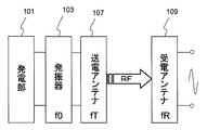
- FIG. 1 shows an example of a basic configuration of a wireless power transmission device according to the present invention.
- the wireless power transmission device includes a first wireless power transmission unit 10a and a second wireless power transmission unit 10b whose outputs are connected in parallel.
- Each of the first and second wireless power transmission units 10a and 10b includes an oscillator 103 that outputs RF energy of frequency f0, a power transmission antenna 107 that receives and transmits RF energy of frequency f0 from the oscillator 103, and a power transmission antenna 107.
- a power receiving antenna 109 that receives at least a part of the RF energy transmitted by the magnetic field coupling by resonance magnetic field coupling.
- the phase of the RF energy output from each oscillator 103 is adjusted by the control unit 192.
- a difference (phase difference) between the phase of the resonant magnetic field 195a in the first wireless power transmission unit 10a and the phase of the resonant magnetic field 195b in the second wireless power transmission unit 10b is set to a predetermined value.
- the phase difference between the resonant magnetic field 195a in the first wireless power transmission unit 10a and the resonant magnetic field 195b in the second wireless power transmission unit 10b is set to 90 degrees or more and 180 degrees or less.
- FIG. 2A and 2B are waveform diagrams schematically showing the phase difference between the resonant magnetic fields 195a and 195b.
- the phase difference ⁇ res has a value of 90 degrees or more and 180 degrees or less.
- FIG. 2B shows a waveform example of the resonant magnetic fields 195a and 195b when the phase difference ⁇ res is equal to 180 degrees.
- phase difference when the phase difference between the two resonance magnetic fields of interest is expressed by (360 ⁇ n + ⁇ ) degrees (n is an integer, ⁇ is a real number between 0 and less than 360), ⁇ degrees and (360 ⁇ The smaller value of ⁇ ) degrees is defined as “phase difference”. Therefore, the maximum value of the phase difference is 180 degrees.
- the control unit 192 illustrated in FIG. 1 includes, for example, a plurality of pulse generators that generate switching pulses that define the timing of starting oscillation of the corresponding oscillator 103, and a control unit that controls the operation of these pulse generators. Is doing. A configuration example of the control unit 192 will be described later.
- the first and second wireless power transmission units 10 a and 10 b are arranged in parallel, and the RF energy received by the power receiving antenna 109 is synthesized by the synthesis unit 199. As a result, the synthesized RF energy is output from the wireless power transmission system and applied to the load 133a.
- the phase difference is preferably zero.
- the phases in the combining unit 199 are matched by adjusting the transmission line distance (line length) from each power receiving antenna 109 to the combining unit 199.
- FIG. 3 is a diagram showing a modified example of the wireless power transmission apparatus of FIG.
- a difference from the configuration of FIG. 1 is that a phase adjustment unit 135 is inserted between the power receiving antenna 109 and the combining unit 199.
- the phase adjustment unit 135 makes the phase in the combining unit 199 coincide by advancing or delaying at least one phase of the RF energy output from the power receiving antenna 109 in the first and second wireless power transmission units 10a and 10b.
- It has a circuit.
- Such a circuit can be, for example, a reactance adjustment circuit having a capacitor element and an inductor element.
- FIG. 4 is a diagram illustrating another modification of the wireless power transmission device of FIG.
- the difference from the configuration of FIG. 1 is that the connection of two wires that transmit RF energy output from the first and second wireless power transmission units 10a and 10b is reversed.
- a pair of wire pairs composed of a combination of two wires is required.
- a return current flows through the other wiring, and the phase of the current in both wirings is reversed.
- the power receiving antenna 109 and the second power in the first wireless power transmission unit 10a are If the combination of the polarities of the wire pairs connected to the power receiving antenna 109 in the wireless power transmission unit 10b is reversed, the RF energy received by the power receiving antenna 109 in the first wireless power transmission unit 10a and the second wireless power The phase of the RF energy combining unit 199 received by the power receiving antenna 109 in the power transmission unit 10b can be matched.
- the phase difference of the RF energy output from the power receiving antenna 109 does not need to be strictly 180 degrees.
- the configuration of FIG. 4 is advantageous under the condition that the distance d between adjacent power receiving antennas is within an electrical length range of several degrees or less with respect to the transmission frequency wavelength ⁇ . For example, assuming the arrangement of solar power generation modules at 1 m intervals, if the transmission frequency is 1 MHz, the wavelength ⁇ at the transmission frequency is 300 m, and d corresponds to an electrical length of 1.2 degrees. In such a case, it is preferable to adopt the configuration of FIG. 4 that is simpler than the configuration of FIG.
- the number of wireless power transmission units included in the wireless power transmission device of the present invention is not limited to two, and may be three or more.
- the oscillation state of the oscillator 103 is controlled so that the phase difference between the closest antenna pair is 90 degrees or more and 180 degrees or less. It is preferable to do.
- FIG. 5 is a block diagram illustrating a configuration example of the wireless power transmission device in FIG. 1.
- Each of the wireless power transmission units 10a and 10b includes an oscillator 103 having an oscillation frequency f0, a power transmission antenna having a resonance frequency fT, and a power receiving antenna 109 having a resonance frequency fR.
- the resonance frequency fT and the resonance frequency fR are Is set equal to the frequency f0.
- the frequency f0 is set to, for example, 50 Hz to 300 GHz, more preferably 10 kHz to 6 GHz, and still more preferably 20 kHz to 20 MHz. Depending on the application, it is set to 20 kHz to 100 kHz, 13.56 MHz, or 2.45 GHz.
- the oscillator 103 receives DC energy (electric power) and converts this DC energy into RF energy having a frequency f0 (DC-RF conversion).
- the oscillation state of the oscillator 103 is controlled by the oscillator driving circuit 190.
- the oscillator drive circuit 190 can be, for example, a pulse generation circuit that generates a pulse signal that defines the oscillation timing of the oscillator 103.
- the pulse signal input from the oscillator driving circuit 190 to the oscillator 103 is typically an analog signal having a rectangular waveform. This pulse signal is a drive signal for switching a high power transistor included in the oscillator 103.
- the oscillator driving circuit 190 and the oscillator 103 are arranged close to each other so that the waveform of the driving signal is not distorted. In the present embodiment, the oscillator driving circuit 190 and the oscillator 103 are separated into separate circuits, but the oscillator driving circuit 190 may be integrated with the oscillator 103.
- the phase of the RF energy output from each oscillator 103 is defined by the input timing of the pulse signal input from the oscillator drive circuit 190.
- the phase of the RF energy 193a output from the oscillator 103 of the first wireless power transmission unit 10a is “ ⁇ ta”
- the phase of the RF energy 193b output from the oscillator 103 of the second wireless power transmission unit 10b is “ ⁇ tb ”.
- the phase of the resonant magnetic field 195a of the first wireless power transmission unit 10a is referred to as “ ⁇ resa”
- the phase of the resonant magnetic field 195b of the second wireless power transmission unit 10b is referred to as “ ⁇ resb”.
- phase of the RF energy 197a output from the power receiving antenna 109 in the first wireless power transmission unit 10a is “ ⁇ ra”
- phase of the RF energy 197b output from the power reception antenna 109 in the second wireless power transmission unit 10b is This is referred to as “ ⁇ rb”.
- each oscillator drive circuit 190 is adjusted by the control unit 192.
- the control unit 192 adjusts the generation timing of the pulse signal generated by each oscillator driving circuit 190, thereby the phase ⁇ ta of the RF energy 193a output from the oscillator 103 of the first wireless power transmission unit 10a, and the second
- the difference from the phase ⁇ tb of the RF energy 193b output from the oscillator 103 of the wireless power transmission unit 10b can be set to a value between 90 degrees and 180 degrees.
- control unit 192 and the plurality of oscillator driving circuits 190 since a control signal composed of a digital signal is preferably transmitted, the two may be separated from each other.
- the control unit 192 and the plurality of oscillator driving circuits 190 can be connected by wire, but are preferably connected by wireless communication. In this manner, the control unit 192 functions as a synchronization adjustment unit that adjusts the timing at which the drive signals are input to the corresponding oscillators from the plurality of oscillator drive circuits 190, respectively.
- RF energy 193a and 193b output from the oscillator 103 are input to the power transmission antenna 107 connected to the oscillator 103, respectively.
- the power transmitting antenna 107 and the power receiving antenna 109 which are designed to have the same resonance frequency are coupled in a circuit by the overlapping of the resonance magnetic fields formed by the resonators.
- the power receiving antenna 109 is an RF transmitted from the power transmitting antenna 107. At least a portion of the energy can be received.
- the power receiving antenna 109 is not in contact with the power transmitting antenna 107 and is separated from the power transmitting antenna 107 by a distance of, for example, several millimeters to several meters.
- the “antenna” in the wireless power transmission device of the present invention is a component for performing energy transmission between two objects using coupling using a proximity component (evanescent tail) of the electromagnetic field of the resonator.
- a proximity component evanescent tail
- energy loss that occurs when electromagnetic waves are propagated far away does not occur, so that power can be transmitted with extremely high efficiency.
- energy transmission using such a coupling of resonant magnetic fields there is less loss compared to known wireless power transmission using Faraday's law of electromagnetic induction.
- energy can be transmitted between two resonators (antennas) separated by several meters, for example.
- frequency fT is equal to frequency fR
- fT is defined as a case where the following Expression 1 is satisfied.
- QT is a Q value as a resonator of the power transmitting antenna
- QR is a Q value as a resonator of the power receiving antenna.
- the resonance frequency is X and the Q value of the resonator is Qx
- the band in which the resonance of the resonator occurs corresponds to X / Qx. If a relationship of
- FIG. 6 is a diagram showing an equivalent circuit of the power transmitting antenna 107 and the power receiving antenna 109.
- the power transmission antenna 107 in the present invention is a series resonance circuit in which a power transmission inductor 107a and a first capacitor element 107b are connected in series.
- the power receiver antenna 109 is a parallel circuit in which a power receiver inductor 109a and a second capacitor element 109b are connected in parallel. It is a resonant circuit. Note that the series resonance circuit of the power transmission antenna 107 has a parasitic resistance component R1, and the parallel resonance circuit of the power reception antenna 109 has a parasitic resistance component R2.
- the inductance of the power transmission inductor 107a is L1
- the inductance of the power reception inductor 109a is L2
- the coupling coefficient between the power transmission antenna 107 and the power reception antenna 109 is k
- the step-up ratio will be defined as the voltage ratio of input / output energy in a corresponding circuit block (including a circuit block group to which a plurality of circuit blocks are connected) in the system.
- the step-up ratio is Vac / Vdc.
- the circuit block is an element such as the oscillation unit 103, the power transmission antenna 107, the power reception antenna 109, the power generation unit 101 and the rectifier 115 described later.
- low voltage energy can be boosted efficiently during transmission.
- FIG. 7 is a schematic diagram of a power generator according to the present invention.
- FIG. 8 shows a part of the configuration of the power generator according to the present invention.
- each power generation unit 131a, 131b includes a power generation unit (power generation device) 101 that supplies DC energy to the oscillator 103.
- Other configurations are the same as those shown in FIG.
- the power generation device of the present invention even when the output voltage of the power generation unit 101 is low, it is possible to output high voltage power due to the boosting effect. Therefore, according to the power generation device of the present invention, for example, low voltage energy (power) generated by a power generation unit (solar power generation unit) configured from a solar cell (cell) can be efficiently boosted during transmission. . For this reason, the number of cells to be connected in series can be greatly reduced. As a result, it is possible to provide a new solar power generation apparatus suitable for popularization that can reduce the installation cost and the maintenance cost.
- FIG. 9 is a schematic diagram showing an example of use of a power generation device including a wireless power transmission device according to the present invention.
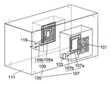
- the illustrated power generation apparatus includes a power generation unit 101 installed outside (outdoors) of a building 200 and a wireless transmission unit 105 for transmitting power to an electronic device existing inside the building 200. Since the power generation unit 101 in this example generates power with sunlight, the power generation unit 101 may also be referred to as the solar power generation unit 101 hereinafter. However, the power generation unit of the present invention is not limited to the solar power generation unit.
- the solar power generation unit 101 has a plurality of connected solar cells as power generation devices.
- the wireless transmission unit 105 includes a power transmission antenna 107 and a power reception antenna 109 that face each other via a wall 111 of the building 200.
- the power transmission antenna 107 is connected to the outdoor solar power generation unit 101, and the power reception antenna 109 is connected to an indoor electronic device. Note that the solar power generation unit 101 does not need to be installed on the roof, and may be installed on the wall 111 of the building 200 or may be installed in another building.
- the power receiving antenna 109 is arranged inside the building 200, but the position of the power receiving antenna 109 is not limited to this example.
- the entire resonant antenna pair formed by the power transmitting antenna 107 and the power receiving antenna 109 may be installed outside the building 200 (roof or wall surface). In that case, the RF energy received by the power receiving antenna 109 can be transmitted to the inside of the building 200 by wire or wirelessly.
- the power generation device constituting the power generation unit in the present invention is not limited to the solar cell, and may be another power generation device.
- the power generation unit may have a fuel cell. Since the fuel cell outputs DC energy having a relatively low voltage and is used in connection with a high voltage system, the boosting effect of the present invention is useful.
- FIG. 10 is a diagram showing a part of the configuration of another wireless power transmission apparatus according to the present invention.
- the wireless power transmission device is different from the above-described wireless power transmission device (FIG. 6) in that a rectifier circuit (rectifier) 115 connected to the power receiving antenna 109 is provided. Due to the function of the rectifier circuit 115, it becomes possible to output DC energy from the wireless power transmission device.
- FIG. 11 shows a part of the configuration of the power generation device of the present invention provided with this type of wireless power transmission device. According to the power generation device of FIG. 11, even if the power generation unit 101 that outputs low-voltage DC energy is used, the DC energy boosted to a sufficiently high voltage can be output due to the boosting effect during wireless power transmission. .
- RF energy received by the power receiving antenna 109 may be converted to alternating current instead of direct current.
- FIG. 12 is a perspective schematic diagram showing the present embodiment
- FIG. 13 is an equivalent circuit diagram of the wireless transmission unit 105 shown in FIG. 12 and 13, the same reference numerals are assigned to the components corresponding to the components shown in FIGS. 5 and 6.
- the power generation apparatus of the present embodiment includes a plurality of power generation units whose outputs are connected in parallel.
- Each power generation unit includes a power generation unit 101, an oscillator 103, and a power generation unit 101 as illustrated in FIG. 12.
- the wireless transmission unit 105 is connected in series.
- the power generation unit 101 in the present embodiment has a plurality of solar cells (cells) connected in series.
- the solar cell it is preferable to use a crystalline silicon solar power generation element from the viewpoint of improving the power generation efficiency.
- the solar cell that can be used in the present invention may be various solar power generation elements using compound semiconductor materials such as gallium arsenide and CIS, or various solar power generation elements using organic materials. There may be.
- the crystal structure of the semiconductor used may be any of single crystal, polycrystal, and amorphous.
- a tandem solar power generation element in which various semiconductor materials are stacked may be used.
- an amplifier capable of realizing a highly efficient and low distortion characteristic such as a class D, a class E, or a class F can be used, or a Doherty amplifier may be used.
- a high-efficiency sine wave may be generated by arranging a low-pass filter or a band-pass filter after the switching element that generates an output signal including a distortion component.
- the wireless transmission unit 105 includes a power transmission antenna 107 and a power reception antenna 109.
- the power transmitting antenna 107 and the power receiving antenna 109 are preferably arranged so as to face each other.
- the arrangement of the antennas 107 and 109 is not limited to the opposed arrangement, and it is sufficient that the antennas 107 and 109 are arranged so as not to be orthogonal to each other.
- the direct current energy generated by the power generation unit 101 is converted into RF energy by the oscillator 103 with high efficiency.
- the RF energy is wirelessly transmitted by the wireless transmission unit 105 through the space (wall 111) wall and is output from the output terminal 119.
- the illustrated power transmission antenna 107 is a series resonance circuit including a power transmission inductor 107a and a first capacitance element 107b
- the power reception antenna 109 is a parallel resonance circuit including a power reception inductor 109a and a second capacitance element 109b.
- the resonance frequency fT of the power transmission antenna 107 and the resonance frequency fR of the power reception antenna 109 are set to be approximately equal to the frequency f0 of the RF energy generated by the oscillator 103, respectively.
- the output impedance Zout of the power receiving antenna 109 in this embodiment is set to a value higher than the input DC impedance Zidc of the oscillator 103.
- the distance between the power transmitting antenna 107 and the power receiving antenna 109 can be set to a distance of several millimeters to several meters, for example, and even if the wall 111 exists between them, high efficiency is achieved.
- the output impedance Zoc of the oscillator 103 and the power transmission antenna are in a state where the output terminal of the power reception antenna 109 is connected to a load. It is preferable to make the input impedance Zin of 107 equal. Similarly, it is preferable that the output impedance Zout of the power receiving antenna is equal to the resistance value R of the connected load in a state where the oscillator 103 is connected to the power transmitting antenna 107.
- the phrase “two impedances are“ equal ”” is not limited to the case where the impedances are exactly the same, but includes the case where the two impedances are substantially equal. It is defined to include the case of 25% or less.
- the wall 111 does not need to exist between the power transmission antenna 107 and the power reception antenna 109, and the power transmission antenna 107 and the power reception antenna 109 may face each other without an obstacle. Further, the thing separating the power transmitting antenna 107 and the power receiving antenna 109 may be a roof.
- both the power transmitting antenna 107 and the power receiving antenna 109 may be disposed indoors or may be disposed outdoors. Even in such a case, boosting can be performed when wireless power transmission is performed between two antennas.
- the connection between the outdoor solar power generation unit 101 and the power transmission antenna 107 is, for example, by wire through an opening provided in the wall 111 of the building 200. Can be realized.
- the connection between the indoor electronic device and the power reception antenna 109 is also realized by, for example, wired via an opening provided in the wall 111 of the building 200 Can be done.
- the efficiency of wireless power transmission in the present embodiment depends on the distance between the power transmitting antenna 107 and the power receiving antenna 109 (antenna spacing) and the magnitude of loss of the circuit elements constituting the power transmitting antenna 107 and the power receiving antenna 109.
- the “antenna interval” is substantially the interval between the two inductors 107a and 109a.
- the antenna interval can be evaluated based on the size of the antenna arrangement area (area occupied by the antenna).
- the power transmitting inductor 107a and the power receiving inductor 109a are both spread in a plane and are disposed so as to face each other in parallel.
- the size of the antenna arrangement area means the size of the antenna arrangement area having a relatively small size.
- the diameter of the circle is used. It is defined as the length of one side, and in the case of a rectangle, the length of the short side of the rectangle. According to the present embodiment, even when the antenna interval is about 1.5 times the size of the antenna arrangement area, it is possible to transmit energy with a wireless transmission efficiency of 90% or more.
- the output impedance of the wireless transmission unit 105 can be increased by 7832 times or more with respect to the input impedance.
- the power transmission inductor 107a and the power reception inductor 109a in the present embodiment have spiral structures with the number of turns N1 and N2, respectively (N1> 1, N2> 1), but may have a loop structure with one number of turns. Good.
- These inductors 107a and 109a do not need to be composed of a single conductor pattern, and may have a structure in which a plurality of laminated conductor patterns are connected in series.
- the power transmission inductor 107a and the power reception inductor 109a can be suitably formed from a conductor such as copper or silver having good conductivity. Since the high frequency current of RF energy flows concentrically on the surface of the conductor, the surface of the conductor may be coated with a high conductivity material in order to increase power generation efficiency. If the inductors 107a and 109a are formed from a configuration having a cavity in the center of the cross section of the conductor, weight reduction can be realized. Furthermore, if the inductors 107a and 109a are formed using a parallel wiring structure such as a litz wire, the conductor loss per unit length can be reduced, so that the Q value of the series resonant circuit and the parallel resonant circuit can be improved. This enables power transmission with higher efficiency.
- a conductor such as copper or silver having good conductivity. Since the high frequency current of RF energy flows concentrically on the surface of the conductor, the surface of the conductor may be coated with a high conductivity material in
- a magnetic body may be arranged around the power transmission inductor 107a and / or the power reception inductor 109a, it is not preferable to set the coupling coefficient between the power transmission inductor 107a and the power reception inductor 109a to an extremely high value. For this reason, it is more preferable to use an inductor having an air-core spiral structure in which the coupling coefficient between the inductors 107a and 109a can be set to an appropriate value.
- Each inductor generally has a coil shape. However, it is not limited to such a shape. At high frequencies, a conductor having a certain line length has an inductance and functions as an inductor. As another example, a bead-like ferrite simply passed through a conductive wire functions as an inductor.
- any type of capacitor having, for example, a chip shape or a lead shape can be used for the first and second capacitor elements 107b and 109b. It is also possible to cause the capacitance between the two wirings via air to function as the first and second capacitor elements 107b and 109b.
- the first and second capacitor elements 107b and 109b are formed of MIM capacitors, a low-loss capacitor circuit can be formed using a known semiconductor process or multilayer substrate process.
- the protective device 117 is preferably waterproofed.
- the power transmitting antenna 107 and the power receiving antenna 109 are preferably arranged as close as possible.
- the position in the protection device 117 may be adjusted for the purpose of adjusting the boost ratio to a desired value.
- the protection device 117 may be directly fixed to an external member such as the wall 111 or the roof. By providing the protection device 117 and the external member with a ferromagnetic material and a magnet, respectively, as long as the magnetic field coupling strength between the power transmission antenna 107 and the power receiving antenna 109 is not affected, the magnetic material acts between the ferromagnetic material and the magnet.
- the protective device 117 may be detachably attached to the external member using magnetic force.
- the protection device 117 may be detachably attached to the external member by providing a suction cup on one of the protection device 117 and the external member.
- the power transmitting antenna 107 on the power transmission side and the power receiving antenna 109 on the power receiving side are coupled with a coupling coefficient k.
- the coupling coefficient is derived from the following equation by measuring two resonance frequencies fL and fH that are separated when two resonators (antennas 107 and 109) that resonate at the same frequency f0 are brought close to each other.
- the frequency f0 of the oscillator 103 is preferably set in the vicinity of the resonance frequencies fL and fH. More specifically, when the Q values of the coupled resonator pair at the resonance frequencies fL and fH are QL and QH, respectively, it is preferable to set f0 so that the following Expression 3 is satisfied. (Formula 3) fL ⁇ fL / QL ⁇ f0 ⁇ fH + fH / QH
- the coupling coefficient k is the same index as a known coupling coefficient conventionally used as an index of coupling strength between inductors or resonators.
- the coupling coefficient k is a numerical value that satisfies the relationship 0 ⁇ k ⁇ 1.
- the configuration and arrangement relationship of the inductor pair is designed so that the coupling coefficient k is as large as possible and approximately equal to 1.
- the high-frequency current flowing through the power transmission inductor 107a is IL1
- the high-frequency current IL2 flowing through the power reception inductor 109a the high-frequency current IC2 flowing through the second capacitor 109b
- the inductance L2 of the power reception inductor 109a the parasitic resistance R2 of the power reception inductor 109a
- the following equation is derived. (Expression 6) (R2 + j ⁇ L2)
- ⁇ IL2 + j ⁇ M ⁇ IL1 IC2 / (j ⁇ C2)
- the magnitude of the high-frequency current (output current) I2 generated in the power receiving antenna 109 is derived by the following (Equation 11).
- I2 k ⁇ (L1 / L2) 0.5 ⁇ IL1
- Vr (Voc / k) ⁇ (L2 / L1)
- Zr (Voc / k) 2 ⁇ (L2 / L1)
- the step-up ratio Vr is equal to 2 when the relationship of (L2 / L1) ⁇ 4 ⁇ (k / Voc) 2 is satisfied.
- a boost ratio Vr of 2 or more can be realized.
- the wireless power transmission device disclosed in Patent Document 2 energy is transmitted between two magnetic resonators.
- the wireless power transmission device adopts the same resonant circuit configuration in the two resonators. Therefore, the boosting effect does not appear during transmission.
- the output voltage increase effect obtained by the wireless power transmission device of the present invention employs a series resonance structure on the power transmission antenna side and a parallel resonance structure on the power reception antenna side. This is a new effect that occurs when energy is transmitted.
- the series resonant circuit and the parallel resonant circuit can also be used in a conventional wireless communication system represented by an RF tag.
- the termination impedance of the measurement terminal of the measuring instrument used for the high frequency block characteristic test of the wireless communication system and the high frequency cable characteristic impedance are basically set to 50 ⁇ . Therefore, at the connection point with the antenna of the wireless communication system, it is common to connect the circuit blocks in accordance with the impedance of 50 ⁇ in both the transmitting device and the receiving device.
- the input / output impedance conversion ratio Zr in the wireless transmission unit according to the present invention is set so as to be extremely high, such as exceeding 100 or exceeding 20000 depending on conditions in the embodiments described later. .
- Such a high input / output impedance conversion ratio Zr is not considered in the conventional communication system.
- the boosting effect can be realized by increasing the ratio of the number of turns N2 of the power receiving inductor to the number of turns N1 of the power transmission inductor.
- the transformer booster circuit it is necessary to increase the number of turns N2 to 10 times or more the number of turns N1.
- a large increase in the number of turns N2 causes the parasitic resistance component R2 in the power receiving inductor to increase proportionally, leading to a decrease in transmission efficiency.
- the boosting effect in the conventional transformer technology is limited to a linear effect with respect to the turns ratio, whereas in the present invention, even if the turns N1 and the turns N2 are set to the same value. , Non-linearly high Zr can be obtained.
- the boost ratio Vr can be increased by setting the inductance L2 to be larger than the inductance L1.
- FIG. 14 is a diagram showing an embodiment in which the number of turns N2 of the power receiving inductor 109a is set larger than the number of turns N1 of the power transmitting inductor 107a in order to increase the inductance L2 of the power receiving inductor 109a.
- N2 / N1 is larger than 1, it is possible to realize a high boosting ratio with a lower loss than when boosting using a known transformer boosting circuit.
- the area where the power receiving antenna 109 is formed is made larger than the area where the power transmitting antenna 105 is formed. May also be enlarged.
- FIG. 15A shows an arrangement area 113 of the power receiving antenna 109 projected perpendicularly to the arrangement plane of the power transmission antenna 107.
- the “arrangement plane” of the power transmission antenna 107 is defined as one plane (first arrangement plane) including the front surface of the power transmission inductor 107a.
- FIG. 15B is a cross-sectional view showing the arrangement surface 240 of the power transmission inductor 107a.
- the power transmission inductor 107 a in the example of FIG. 15B is parallel to the arrangement surface 240.
- the arrangement area of the power receiving antenna is defined as an area surrounded by the outline of the power receiving inductor 109a projected perpendicularly to the arrangement surface 240 of the power transmitting antenna 107.
- FIG. 15 (a) shows a power transmission inductor 107a projected perpendicularly to the arrangement surface of the power transmission antenna 107.
- FIG. 15A the power transmission inductor 107 a projected on the arrangement surface of the power transmission antenna 107 exists inside the arrangement area 113 and is close to the edge of the arrangement area 113.
- the power transmission antenna may be set larger than the power receiving antenna after setting the antenna shape and size to an asymmetric combination.
- the antenna arrangement relationship is not limited to the example illustrated in FIG. 15, and may be an arrangement relationship in which the power transmission antenna 107 and the power reception antenna 109 are interchanged. That is, “power transmitting antenna 107” in FIG. 15 may be replaced with “power receiving antenna 109”, and “arrangement region 113” may be replaced with “arrangement region of power transmitting antenna 107”.
- the “arrangement area of the power transmission antenna 107” is an area surrounded by the outline of the inductor 107a projected on the arrangement surface of the power reception antenna 109.
- the “arrangement surface of the power receiving antenna 109” is defined as one plane (second arrangement surface) including the front surface of the power receiving inductor 109a.
- the first arrangement surface and the second arrangement surface are preferably parallel to each other, but they do not have to be strictly parallel.
- the power transmission inductor 107a and the power reception inductor 109a do not need to have a planar shape.
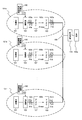
- FIG. 16 includes a plurality of power generation units 131a, 131b,..., 131n each including a power generation unit 101, an oscillator 103, a power transmission antenna 107, and a power reception antenna 109. Output energies received by the plurality of power receiving antennas 109 are combined in parallel to form total output energy.
- the angle is preferably set to 180 degrees.
- the phase ⁇ ta of the RF energy 193a transmitted from the corresponding oscillator 103 is controlled by the oscillator driving circuit 190 in the first power generation unit 131a.
- the phase ⁇ tb of the RF energy 193b transmitted from the corresponding oscillator 103 is controlled by the oscillator driving circuit 190 in the second power generation unit 131b.
- each oscillator driving circuit 190 is connected to the control unit 192 (FIG. 5) by wire or wirelessly.
- the RF energy 193a output from the oscillator 103 in the first power generation unit 131a and the RF energy 193b output from the oscillator 103 in the second power generation unit 131b are both high-frequency energy having the same frequency f0. .
- the absolute value ⁇ t (
- ) of the phase difference between the RF energy 193a and the RF energy 193b is controlled.
- ⁇ t is controlled to be 90 degrees or more and 180 degrees or less, preferably 180 degrees.
- the ⁇ t can be set equal to ⁇ res by setting the inductance, size, and number of turns of the power transmission antenna 107 in each power generation unit 131a, 131b to be equal. 3 and 4 so that the phase ⁇ ra of the RF energy 197a output from the power receiving antenna 109 in the first power generation unit 131a and the phase ⁇ rb of the RF energy 197b in the second power generation unit are finally in phase. It is preferable to employ the configuration described with reference.
- the absolute value ⁇ res of the phase difference between the resonance magnetic fields 195a and 195b is 90 degrees or more and 180 degrees or less, at least a part of the vector components of the two resonance magnetic fields 195a and 195b cancel each other, so that electromagnetic leakage to the surrounding space is prevented. Can be reduced. If ⁇ res is 180 degrees, the two resonant magnetic fields cancel each other, so that electromagnetic leakage to the surrounding space can be suppressed. This effect is effective for a magnetic field source pair that is much shorter than the wavelength (generally 1/8, preferably 1/16 or less of the wavelength of the frequency f0). The shorter the distance between the source pair, the more effective. Therefore, when there are three or more resonant antenna pairs in the power generation apparatus of the present invention, the effect of suppressing electromagnetic leakage is improved by setting ⁇ res to 90 degrees or more, more preferably 180 degrees between the most adjacent resonant antenna pairs.
- N is an integer of 4 or more resonant antenna pairs
- ⁇ res is 90 degrees or more for N / 2 adjacent resonant antenna pairs. Setting to 180 degrees or less, more preferably 180 degrees is a condition for maximizing the effect of suppressing the total electromagnetic leakage from the apparatus. Further, even when N is an odd number, it is possible to set ⁇ res to 90 degrees or more and 180 degrees or less, more preferably 180 degrees for (N ⁇ 1) / 2 adjacent resonant antenna pairs, so that the total electromagnetic from the device This is a condition that maximizes the suppression effect of leakage.
- FIG. 17 is a schematic top view when four pairs of transmission / reception resonant antennas 141a to 141d are present in a square lattice arrangement in the power generator of the present invention.
- the transmission / reception resonance antenna pair 141a and the transmission / reception resonance antenna pair 141b whose center-to-center distance is d1 ( ⁇ d3) than the transmission / reception resonance antenna pair 141a and the transmission / reception resonance antenna pair 141d whose distance between the centers is d3.
- the transmission / reception resonance antenna pair 141a and the transmission / reception resonance antenna pair 141c whose distance between the centers is d2 ( ⁇ d3) satisfy ⁇ res ⁇ 90 degrees.
- the power generator of the present invention it is preferable to satisfy the magnetic field suppression condition (90 degrees ⁇ ⁇ res ⁇ 180 degrees) between the nearest transmitting / receiving resonant antenna pair.
- the sign “+” indicates a resonant magnetic field having the same phase
- the sign “ ⁇ ” indicates a resonance whose phase is different from 90 degrees to 180 degrees with respect to the resonant magnetic field having the sign “+”. The magnetic field is shown.
- the first point of difference between the power generation apparatus of the present embodiment and the power generation apparatus of the first embodiment is that a rectifier circuit 115 that converts RF energy into DC energy is connected in series after the combining unit 199. .
- a rectifier circuit 115 that converts RF energy into DC energy is connected in series after the combining unit 199. .
- the same effect as that of the power generation device in the first embodiment can be obtained, and further, DC power can be obtained as an output.
- the output terminal of the rectifier circuit 115 is connected to a DC load or a DC load system (not shown) while the oscillator 103 It is preferable that the output impedance Zoc and the input impedance Zin of the power transmission antenna 107 are substantially equal. Similarly, in the state where the oscillator 103 is connected to the power transmission antenna 107, the output impedance Zrout of the rectifier circuit 115 is set to be approximately equal to the resistance value R of the DC load or DC load system (not shown) to be connected. Is preferred.
- the rectifier circuit 115 includes a circuit that performs rectification by various methods, and both-wave rectification and a bridge rectification circuit can be used.
- 20A is a circuit diagram of a half-wave voltage doubler rectifier circuit
- FIG. 20B is a circuit diagram of a double-wave voltage doubler rectifier circuit.
- there is a high voltage rectifier circuit system that can realize a boost ratio of 3 times or more. Any of these rectifier circuits can be applied to the present invention.
- the voltage doubler rectifier circuit illustrated in FIG. 20 it becomes possible to output a DC voltage boosted to twice the RF voltage input to the rectifier circuit 115.
- a rectifier circuit 115 in addition to the boosting effect in the wireless transmission unit 105, a further boosting effect can be realized.
- the boost ratio Vr and the impedance conversion ratio Zr derived for the first embodiment are rewritten into the following (Expression 15) and (Expression 16) using the boost ratio Vrr in the rectifier circuit 115, respectively.
- Vr (Voc ⁇ Vrr / k) ⁇ (L2 / L1)
- Zr (Voc ⁇ Vrr / k) 2 ⁇ (L2 / L1)
- the step-up ratio can be made larger than 1 when the relationship of (L2 / L1)> (k / (Voc ⁇ Vrr)) 2 is satisfied. Become.
- a DC power feeding system can be realized.
- FIG. 21 is a block diagram of the power generation device according to this embodiment.
- the same reference numerals are given to the same components as those of the power generation device in the above-described embodiment, and the detailed description thereof is omitted.
- the 21 includes a plurality of power generation units 131a, 131b,... 131n connected in parallel.
- the power generation units 131a to 131n in the present embodiment are all the power generation device of the second embodiment. However, in order to obtain the effects of the present invention, at least two power generation devices connected in parallel are the power generation devices of the present invention. I just need it.
- Each of the power generation units 131a to 131n includes a solar power generation unit 101, an oscillator 103, a power transmission antenna 107, a power reception antenna 109, and a rectifier circuit 115 connected in series.
- the direct current energy generated by the photovoltaic power generation unit 101 is converted into RF energy by the oscillator 103 with high efficiency.
- This RF energy is transferred in a non-contact manner between the power transmitting antenna 107 on the power transmission side and the power receiving antenna 109 on the power receiving side, then converted into DC energy by the rectifier circuit 115, and output from each of the power generation units 131a to 131n.
- the DC energy (electric power) is added by parallel connection and then supplied to the load 133a.
- the output voltage obtained from each of the power generation units 131a to 131n is drastically increased as compared with the output voltage obtained by each photovoltaic power generation unit. Therefore, even if the power generation units 131a to 131n are connected in parallel, a value closer to the voltage value required by the load 133a can be realized.
- the power generation units 131a to 131n are connected in parallel, even when some of the characteristics of the power generation units 131a to 131n are deteriorated or when the sunlight irradiation conditions for the power generation units 131a to 131n are different, It is possible to obtain more stable characteristics than the power generation apparatus.
- the load 133a is, for example, a general electric device or a storage battery.
- the load 133a may be an inverter function circuit for converting direct current to alternating current, a step-up / step-down function circuit, or a power conditioner circuit having a composite function of both functions.
- the power generation device may be connected in series in a part of the power generation device in the present embodiment.
- the first point that the power generation device of the present embodiment is different from the power generation device in the second embodiment is that a frequency conversion circuit 189 that converts RF energy into AC energy is connected in series after the combining unit 199, and a plurality of power reception devices are connected. The point is that the received energy received by the antenna 109 is output as AC energy.
- the same effect as that of the power generation device in the first embodiment can be obtained, and AC power that can be sent to the load / system 133b can be obtained as an output.
- the load / system 133b means at least one of a load that can be driven by AC energy or a power system that transmits AC energy, as will be described later. According to the present embodiment, it is also possible to switch between the case where AC energy is output to a load and the case where it is output to a system, as required.
- the output impedance of the oscillator 103 is maintained when the output terminal of the frequency conversion circuit 189 is connected to an AC load or AC system. It is preferable to make the dance Zoc and the input impedance Zin of the power transmission antenna 107 substantially equal.
- the frequency conversion circuit 189 There are various types of circuits in the frequency conversion circuit 189, but a configuration for performing direct frequency conversion, such as a matrix converter system, or a circuit for performing indirect frequency conversion can be employed. In addition, any frequency conversion circuit technology that supports single-phase or three-phase output as the output configuration can be applied to the present invention.
- the boost ratio Vr and the impedance conversion ratio Zr derived for the first embodiment are rewritten into the following (Expression 17) and (Expression 18) using the boost ratio Vcon in the frequency conversion circuit 189, respectively.
- Vr (Voc ⁇ Vcon / k) ⁇ (L2 / L1)
- Zr (Voc ⁇ Vcon / k) 2 ⁇ (L2 / L1)
- the step-up ratio can be made larger than 1 when the relationship of (L2 / L1)> (k / (Voc ⁇ Vcon)) 2 is satisfied. Become.
- a system connection power generator can be realized.
- Vin Vin ⁇ (Voc ⁇ Vcon / k) ⁇ (L2 / L1) 0.5 is the output voltage.
- Vin Vin ⁇ (Voc ⁇ Vcon / k) ⁇ (L2 / L1) 0.5 is the output voltage.
- 202V system 202V ⁇ 20V.
- 182 ⁇ Vout ⁇ 222 it is possible to connect the low-voltage power generation unit output energy to the system.
- the frequency conversion circuit 189 can also have a step-up / step-down function.
- FIG. 23 is a block diagram of the power generation device in the present embodiment.
- the same reference numerals are given to the same components as those of the power generation device in the above-described embodiment, and the detailed description thereof is omitted.
- the 23 includes a plurality of power generation units 131a, 131b,... 131n connected in parallel. In order to obtain the effect of the present invention, it is sufficient that at least two power generation devices connected in parallel are the power generation devices of the present invention.
- Each of the power generation units 131a to 131n includes a solar power generation unit 101, an oscillator 103, a power transmission antenna 107, a power reception antenna 109, and a frequency conversion circuit 189 connected in series.
- the direct current energy generated by the photovoltaic power generation unit 101 is converted into RF energy by the oscillator 103 with high efficiency.
- This RF energy is transferred in a non-contact manner between the power transmitting antenna 107 on the power transmission side and the power receiving antenna 109 on the power receiving side, then converted into AC energy by the frequency conversion circuit 189, and output from each of the power generation units 131a to 131n.
- the AC energy electric power
- it is supplied to the load 133a.
- the output voltage obtained from each of the power generation units 131a to 131n is drastically increased as compared with the output voltage obtained by each photovoltaic power generation unit. Therefore, even if the power generation units 131a to 131n are connected in parallel, a value closer to the voltage value required by the load 133a can be realized.
- the power generation units 131a to 131n are connected in parallel, even when some of the characteristics of the power generation units 131a to 131n are deteriorated or when the sunlight irradiation conditions for the power generation units 131a to 131n are different, It is possible to obtain more stable characteristics than the power generation apparatus.
- the load / system 133b is, for example, a general electric device or storage battery that supports AC input.
- the load / system 133b can include a step-up / down function circuit.
- the power generation device may be connected in series in a part of the power generation device in the present embodiment.
- Example 1 In the power generator of the present invention, a plurality of power generation units are connected in parallel. And pressure
- Example 1 of the present invention will be described.
- the power transmission antenna and power reception antenna were designed so that the resonance frequency was 3 MHz, which is equal to the output frequency of the oscillator.
- the power transmission antenna was manufactured by connecting a power transmission inductor having an inductance of 1.988 ⁇ H and a first capacitor element having a capacitance of 830 pF in series.
- the power receiving antenna was manufactured by connecting a power receiving inductor having an inductance of 1.988 ⁇ H and a second capacitor element having a capacitance of 830 pF in parallel.
- Both the first and power receiving inductors were realized by litz wires configured by arranging 30 parallel copper wires each having a diameter of 80 ⁇ m and arranging them in parallel.
- the outer shape of the two inductors was a square with a side of 36 cm, and the number of turns was set to two.
- the Q value of each antenna (resonator) was 1350.
- the power transmitting antenna and the power receiving antenna were arranged with their formation surfaces facing each other in parallel, and the distance between the opposing surfaces was g (cm). While changing the gap g in the range from 5 cm to 75 cm, optimum input / output impedances Zin and Zout that maximize the wireless transmission efficiency between the resonators for each g value were measured. Actual measurement was performed by the following two-step procedure.
- FIG. 24 is a graph showing g dependence of derived Zin and Zout.
- FIG. 25 is a graph showing the dependency of the input / output impedance conversion ratio Zr and the transmission efficiency on the wireless transmission unit on g.
- FIG. 26 is a graph showing enlarged characteristics in the range of 10 cm ⁇ g ⁇ 40 cm in the graph of FIG.
- the wall thickness is in the range of about 10 cm to 30 cm.
- the gap g is included in this range, a very large Zr of 20 to 363 was obtained.
- the ratio of the number of turns of the secondary coil to the number of turns of the primary coil is set to 12.1 times. There is a need. In the example of the present invention, Zr could be dramatically increased to 147 while using a power transmission antenna and a power reception antenna with a turns ratio of 1.
- Example 2 Two power generation units having the same configuration as that of Example 1 described above were prepared, and their outputs were connected in parallel. Specifically, the distance between the centroids of the two power transmission antennas and the distance between the centroids of the two power reception antennas were respectively moved in parallel and arranged in parallel. The energy received by the two power receiving antennas was synthesized in parallel.
- Example 1a measurement was performed by shifting the phase difference between the outputs of the two oscillators by 30 degrees from 90 degrees to 180 degrees, and Examples 1a-90, 1a-120,.
- Comparative Example 1 the phase difference between the outputs of the two oscillators was set to a value from zero degrees to 60 degrees, and Comparative Examples 1-0, 1-30, and 1-60 were used.
- the wiring of the power transmission inductor in the two power generation units was formed by rotating in the same direction.
- a leakage electromagnetic field evaluation index in Example 1a and Comparative Example 1 the near-field strength at a point 5 m away was derived.
- Comparative Examples a to c Comparative Examples a to c
- Comparative Examples a and b Comparative Examples a to c
- the resonance methods of the two antennas (resonators) in Comparative Examples a and b are equal to each other. That is, in Comparative Example a, each of the two antennas is composed of an LC series resonator, and in Comparative Example b, each of the two antennas is composed of an LC parallel resonator.
- the circuit constant of each resonator was matched with the circuit constant in Example 1.
- a comparative example c configured so that the two antennas do not resonate was also produced.
- the boosting effect and the high-efficiency operation could not be achieved at the same time. Therefore, the parallel operation of the two power generation units and the near-field measurement were not performed.
- Example 1 can achieve a very high step-up ratio Vr while realizing high-efficiency power transmission wirelessly.
- Table 2 shows the near field strength in Example 1a and Comparative Example 1.
- strength in the direction which showed the worst value is shown.
- Example 2 a power generation unit in which a voltage doubler rectifier circuit was connected to the output of the power receiving antenna having the same configuration as that of the power receiving antenna in Example 1 was produced.
- the DC conversion efficiency of the produced half-wave voltage doubler rectifier circuit was 93.4% at a resonance frequency of 3 MHz.
- the direct current energy was 86.4% intensity.
- Example 2 Two power generation units having the same configuration as that of Example 2 described above were prepared, and their outputs were connected in parallel. Specifically, the distance between the centroids of the two power transmission antennas and the distance between the centroids of the two power reception antennas were respectively moved in parallel and arranged in parallel. The energy received by the two power receiving antennas was rectified by the rectifier circuit and then combined in parallel.
- Example 2a measurement was performed by shifting the phase difference between the outputs of the two oscillators by 180 degrees, whereas in Comparative Example 2, the phase difference between the outputs of the two oscillators was set to zero degrees.
- the wiring of the power transmission inductor in the two power generation units was formed by rotating in the same direction.
- the near-field intensity measurement in all solid angle directions was performed in increments of 10 degrees, and the worst value of Example 2a was 65% lower than that of Comparative Example 2.
- Example 3 As Example 3, a power generation unit in which a bridge rectifier circuit was connected to the power receiving antenna output having the configuration of Example 1 was produced.
- the DC conversion efficiency of the manufactured bridge rectifier circuit was 94.1% at a resonance frequency of 3 MHz.
- the output DC energy of the power generation device was 87.0% of the intensity of the output energy of the photovoltaic power generation unit.
- Example 3 Two power generation units having the same configuration as that of Example 3 described above were prepared, and their outputs were connected in parallel. Specifically, the distance between the centroids of the two power transmission antennas and the distance between the centroids of the two power reception antennas were respectively moved in parallel and arranged in parallel. The energy received by the two power receiving antennas was rectified by the rectifier circuit and then combined in parallel.
- Example 3a the measurement was performed by shifting the phase difference between the outputs of the two oscillators by 180 degrees, whereas in Comparative Example 3, the phase difference between the outputs of the two oscillators was set to zero degrees.
- the wiring of the power transmission inductor in the two power generation units was formed by rotating in the same direction.
- the near field intensity measurement in all solid angle directions was performed in increments of 10 degrees.
- the worst value of Example 3a was 66% lower than that of Comparative Example 3.
- the output voltage of the power generation unit of Example 4 was 308 V, and the power generation efficiency was 87.2%.
- Example 4 Two power generation units having the same configuration as that of Example 4 described above were prepared, and their outputs were connected in parallel. Specifically, the distance between the centroids of the two power transmission antennas and the distance between the centroids of the two power reception antennas were respectively moved in parallel and arranged in parallel. The energy received by the two power receiving antennas was rectified by the rectifier circuit and then combined in parallel.
- Example 4a measurement was performed by shifting the phase difference between the outputs of the two oscillators by 180 degrees, whereas in Comparative Example 4, the phase difference between the outputs of the two oscillators was set to zero degrees.
- the wiring of the power transmission inductor in the two power generation units was formed by rotating in the same direction.
- the near field intensity measurement in all solid angle directions was performed in increments of 10 degrees.
- the worst value of Example 4a was 63% lower than that of Comparative Example 4.
- Example 5 Seven power generation units having the same configuration as that of the power generation unit of Example 4 were arranged in a line, and all of these units were connected in parallel to produce the power generation device of Example 5. With this power generation device, a power generation output with an output voltage of 308 V and 27.5 W was obtained. Similarly, as Comparative Example 5, a power generation apparatus in which 63 photovoltaic power generation cells were connected in series was manufactured. Table 2 below shows the characteristics of Example 5 and Comparative Example 5.
- Example 5 the output voltage was 9.8 times higher although the number of cells in series was much smaller than that in Comparative Example 5. According to the fifth embodiment, it is possible to realize a power generator that provides an optimal voltage value for a DC power supply system at 300V.
- the distance between the centroids of the adjacent power transmission antennas and the centroid of the power reception antennas were 50 cm, respectively.
- the comparative example 5a includes only one set of an oscillator, a power transmission antenna, a power reception antenna, and a rectification unit in the system while including the same number of solar cells as in the fifth embodiment.
- the wiring of the power transmission inductor in all the power generation units was formed by rotating in the same direction.
- the near-field intensity measurement in all solid angle directions was performed in increments of 10 degrees, and the worst value of Example 5 was able to be reduced by 78% with respect to the worst value of Comparative Example 5a.
- the present invention makes it possible to reduce the installation cost of the power generation apparatus and simplify the replacement work when a part of the power generation unit deteriorates.
- the present invention can easily increase the output voltage of the power generation unit, when the power generation unit is configured by connecting power generation elements (solar cells) with low output voltage in series, the number of connected power generation elements Can be greatly reduced. For this reason, it is possible to construct a photovoltaic power generation apparatus that reduces characteristic deterioration with respect to partial shading and realizes stable power supply. In addition, it is possible to suppress the leakage electromagnetic component from the wireless power transmission site.
- the boosting effect of the present invention is also useful in a fuel cell system that is a power generation device that functions by connecting output energy from a power generation device that is output at a low voltage to a high voltage system.
- Power generation unit (solar power generation unit) DESCRIPTION OF SYMBOLS 103 Oscillator 10a 1st wireless power transmission part 10b 2nd wireless power transmission part 105 Wireless transmission part 107 Power transmission antenna (resonator on the power transmission side) 107a first inductor 107b first capacitor 109 power receiving antenna (power receiving side resonator) 109a Second inductor 109b Second capacitor 111 Wall 113 Power receiving antenna placement area projected onto the power transmission antenna placement surface 115 Rectifier 117 Protection device 119 Output terminal 131a, 131b ...
- Power generation unit 133a Load 133b Load / system 135 Phase adjustment Circuit 141 Transmission / reception resonance antenna pair 141a, 141b, 141c, 141d Transmission / reception resonance antenna pair 189
- Frequency conversion circuit 190 Oscillator drive circuit 192
- 195n Resonant magnetic field 197a, 197b, ... 197n RF energy output from the power receiving antenna 199 Synthesizer
Abstract
Description
(式1) |fT-fR|≦fT/QT+fR/QR
ここで、QTは送電アンテナの共振器としてのQ値、QRは受電アンテナの共振器としてのQ値である。一般に、共振周波数をX、共振器のQ値をQxとした場合、この共振器の共振が生じる帯域はX/Qxに相当する。|fT-fR|≦fT/QT+fR/QRの関係が設立すれば、2つの共振器間で磁気共振によるエネルギ伝送が実現する。
(L2/L1)≧4(k/Voc)2
(L2/L1)≧4(k/(Voc×Vrr))2
この点についても、詳細な説明は後述する。
まず、図12および図13を参照しながら、本発明による発電装置の第1の実施形態を説明する。図12は、本実施形態を示す透視模式図であり、図13は、図12に示す無線伝送部105の等価回路図である。図12、図13において、図5、図6に示した構成要素に対応する構成要素には同じ参照符号を付している。
(式2) k=(fH2-fL2)/(fH2+fL2)
(式3)fL-fL/QL≦f0≦fH+fH/QH
(式4) M=k×(L1×L2)0.5
(式5) I2=-IL2-IC2
(式6) (R2+jωL2)×IL2+jωM×IL1=IC2/(jωC2)
(式7) ωL2=1/(ωC2)
(式8) R2×IL2+jωM×IL1=jωL2×I2
(式9) I2=k×(L1/L2)0.5×IL1-j(R2/ωL2)×IL2
(式10) Q2=ωL2/R2
(式11) I2=k×(L1/L2)0.5×IL1
ここで、高周波電流I2は、送電側の共振器(送電アンテナ107)に入力される高周波電流I1(=送電インダクタ107aを流れる高周波電流IL1)、共振器(アンテナ)間の結合係数k、送電インダクタ107aおよび受電インダクタ109aのインダクタンスL1、L2に依存する。
(式12) Ir=|I2/I1|/Voc=k/Voc×(L1/L2)0.5
(式13) Vr=(Voc/k)×(L2/L1)0.5
(式14) Zr=(Voc/k)2×(L2/L1)
次に、図19を参照しながら、本発明による発電装置の第2の実施形態を説明する。
(式15) Vr=(Voc×Vrr/k)×(L2/L1)0.5
(式16) Zr=(Voc×Vrr/k)2×(L2/L1)
次に、図21を参照しながら、本発明による発電装置の実施形態を説明する。図21は、本実施形態における発電装置のブロック図である。図21において、前述の実施形態における発電装置の構成要素と同一の構成要素には、同一の参照符号を付しており、その詳細な説明は省略する。
次に、図22を参照しながら、本発明による発電装置の第4の実施形態を説明する。
(式17) Vr=(Voc×Vcon/k)×(L2/L1)0.5
(式18) Zr=(Voc×Vcon/k)2×(L2/L1)
次に、図23を参照しながら、本発明による発電装置の実施形態を説明する。図23は、本実施形態における発電装置のブロック図である。図23において、前述の実施形態における発電装置の構成要素と同一の構成要素には、同一の参照符号を付しており、その詳細な説明は省略する。
本発明の発電装置では、複数の発電ユニットが並列に接続される。そして、個々の発電ユニットにおける無線電力伝送によって昇圧を行うことができる。このため、最初に1つの発電ユニットの実施例を説明し、その後、複数の発電ユニットを備える発電装置の実施例を説明する。
実施例1の場合と同様に、無線伝送部を送受共に共振周波数3MHzの共振器で実現した比較例a、bを作製した。実施例1と比較例a、bとの間にある相違点は、比較例a、bにおける2つのアンテナ(共振器)の共振方式を相互に等しくした点のみにある。すなわち、比較例aでは、2つのアンテナをそれぞれLC直列型共振器から構成し、比較例bでは、2つのアンテナをそれぞれLC並列共振器から構成した。各共振器の回路定数は、実施例1における回路定数と一致させた。更に、2つのアンテナが共振しないように構成された比較例cも作製した。なお、比較例a~cは、昇圧効果と高効率動作の両立が出来なかったため、2つの発電ユニットの並列動作や近傍界測定は行わなかった。


次に、実施例2として、実施例1における受電アンテナの構成と同一の構成を有する受電アンテナの出力に、倍電圧整流回路を接続した発電ユニットを作製した。作製した半波倍電圧整流回路の直流変換効率は、共振周波数3MHzにおいて、93.4%を示した。導入した整流回路では、入力高周波電圧に対して出力直流電圧が2倍の値となる昇圧比Vrr=2の昇圧機能が得られ、太陽光発電部の出力エネルギに対して、本発電ユニットが出力する直流エネルギは86.4%の強度であった。
実施例3として、実施例1の構成の受電アンテナ出力に、ブリッジ整流回路を接続した発電ユニットを作製した。作製したブリッジ整流回路の直流変換効率は、共振周波数3MHzにおいて、94.1%を示した。導入した整流回路では、太陽光発電部の出力エネルギに対して、本発電装置の出力直流エネルギは87.0%の強度であった。
実施例3の条件を一部変更し、Voc=1.52、g=15cmの条件で実施例4の発電ユニットを作製した。実施例4の発電ユニットの出力電圧は308Vであり、発電効率は87.2%であった。
実施例4の発電ユニットの構成と同じ構成を有する7個の発電ユニットを一列に並べ、これら全て並列に接続し、実施例5の発電装置を作製した。この発電装置では、出力電圧308V、27.5Wの発電出力を得た。同様に、比較例5として太陽光発電セルを63個直列に接続した発電装置を作製した。以下の表2に、実施例5と比較例5の特性を示した。

103 発振器
10a 第1の無線電力伝送部
10b 第2の無線電力伝送部
105 無線伝送部
107 送電アンテナ(送電側の共振器)
107a 第1インダクタ
107b 第1キャパシタ
109 受電アンテナ(受電側の共振器)
109a 第2インダクタ
109b 第2キャパシタ
111 壁
113 送電アンテナの配置面へ投影した受電アンテナの配置領域
115 整流器
117 保護装置
119 出力端子
131a、131b・・・131n 発電ユニット
133a 負荷
133b 負荷/系統
135 位相調整回路
141 送受共振アンテナ対
141a、141b、141c、141d 送受共振アンテナ対
189 周波数変換回路
190 発振器駆動回路
192 制御部
193a、193b、・・・193n 発振器から出力されるRFエネルギ
195a、195b、・・・195n 共振磁界
197a、197b、・・・197n 受電アンテナから出力されるRFエネルギ
199 合成部
Claims (32)
- 第1および第2の無線電力伝送部であって、前記第1および第2の無線電力伝送部の各々が、
直流エネルギを周波数f0のRFエネルギに変換する発振器と、
前記RFエネルギを送出する送電アンテナであって、共振周波数fTを有する直列共振回路を構成するように直列に接続された第1インダクタおよび第1容量素子を含む送電アンテナと、
前記送電アンテナによって送出された前記RFエネルギの少なくとも一部を共振磁界の結合によって受け取る受電アンテナであって、共振周波数fRを有する並列共振回路を構成するように並列に接続された第2インダクタおよび第2容量素子を含む受電アンテナと、を備え、
前記共振周波数fTおよび前記共振周波数fRは、前記RFエネルギの周波数f0に実質的に等しく設定され、
前記発振器の昇圧比をVoc、第1インダクタのインダクタンスをL1、第2インダクタのインダクタンスをL2、前記送電アンテナと前記受電アンテナとの結合係数をkとするとき、
(L2/L1)≧4(k/Voc)2を満足する、第1および第2の無線電力伝送部と、
第1および第2の無線電力伝送部における前記受電アンテナから受け取ったRFエネルギを合成して出力する合成部と、
前記第1の無線電力伝送部における前記共振磁界の位相と前記第2の無線電力伝送部における前記共振磁界の位相との位相差θresを90度以上180度以下にするように前記第1および第2の無線電力伝送部における前記発振器を制御する制御部と、
を備える無線電力伝送装置。 - 位相差θresが180度に設定されている請求項1に記載の無線電力伝送装置。
- 前記制御部は、前記第1の無線電力伝送部に含まれる前記発振器から送出されるRFエネルギの位相θtaと、前記第2の無線電力伝送部に含まれる前記発振器から送出されるRFエネルギの位相θtbとを制御し、それによって位相θtaと位相θtbとの間の位相差の絶対値θtを90度180度以下に設定する請求項1または2に記載の無線電力伝送装置。
- 前記位相差の絶対値θtが180度に設定される請求項3に記載の無線電力伝送装置。
- 第1および第2の発電ユニットであって、前記第1および第2の発電ユニットの各々が、
直流エネルギを出力する発電部と、
前記発電部から出力された直流エネルギを周波数f0のRFエネルギに変換する発振器と、
前記RFエネルギを送出する送電アンテナであって、共振周波数fTを有する直列共振回路を構成するように直列に接続された第1インダクタおよび第1容量素子を含む送電アンテナと、
前記送電アンテナによって送出された前記RFエネルギの少なくとも一部を共振磁界の結合によって受け取る受電アンテナであって、共振周波数fRを有する並列共振回路を構成するように並列に接続された第2インダクタおよび第2容量素子を含む受電アンテナと、を備え、
前記共振周波数fTおよび前記共振周波数fRは、前記RFエネルギの周波数f0に実質的に等しく設定され、
前記発振器の昇圧比をVoc、第1インダクタのインダクタンスをL1、第2インダクタのインダクタンスをL2、前記送電アンテナと前記受電アンテナとの結合係数をkとするとき、
(L2/L1)≧4(k/Voc)2を満足する、第1および第2の発電ユニットと、
前記第1および第2の発電ユニットにおける前記受電アンテナから受け取ったRFエネルギを合成して出力する合成部と、
前記第1の発電ユニットにおける前記共振磁界の位相と前記第2の発電ユニットにおける前記共振磁界の位相との位相差θresを90度以上180度以下にするように前記第1および第2の発電ユニットにおける前記発振器を制御する制御部と、
を備える発電装置。 - 前記発電部は、太陽光発電部である請求項3に記載の発電装置。
- 前記太陽光発電部は結晶系シリコンを用いた太陽光発電部である請求項3に記載の発電装置。
- 前記受電アンテナの出力端子と後段の負荷とが接続された状態において、前記発振器の出力インピ-ダンスZocと送電アンテナの入力インピーダンスZinとが相互に実質的に等しい請求項5から7のいずれかに記載の発電装置。
- 前記発振器の出力端子と前記送電アンテナの入力端子とが接続された状態において、前記受電アンテナの出力インピーダンスZoutと後段に接続する負荷の入力インピーダンスとが実質的に等しい請求項5から8のいずれかに記載の発電装置。
- (L2/L1)≧100×(k/Voc)2を満足する請求項5から9のいずれかに記載の発電装置。
- (L2/L1)≧10000×(k/Voc)2を満足する請求項5から10のいずれかに記載の発電装置。
- 前記発電部および前記送電アンテナは、建物の外側に配置され、
前記受電アンテナは、前記建物の内部に設置されている、請求項5から11のいずれかに記載の発電装置。 - 前記第1インダクタおよび前記第2インダクタは、いずれも空芯スパイラル構造を有している請求項5から11のいずれかに記載の発電装置。
- L1<L2である請求項5から13のいずれかに記載の発電装置。
- 前記第2インダクタの巻数N2は前記第1インダクタの巻数N1よりも大きい請求項5から14のいずれかに記載の発電装置。
- 前記第2インダクタの面積は、前記第1インダクタの面積よりも広い請求項5から15のいずれかに記載の発電装置。
- 前記送電アンテナの配置面上に投影された前記第1インダクタは、前記配置面上に投影された前記第2インダクタの輪郭によって規定される領域の内部に含まれ、かつ、前記領域の周縁に寄っている、請求項16に記載の発電装置。
- 前記送電アンテナの配置面上に投影された前記第1インダクタは、前記配置面上に投影された前記第2インダクタの輪郭によって規定される領域の周縁に寄っている、請求項16または17に記載の発電装置。
- 前記第1の発電ユニットにおける前記受電アンテナから出力されるRFエネルギの位相と前記第2の発電ユニットにおける前記受電アンテナから出力されるRFエネルギの位相とを一致させる位相調整部が、前記第1および第2の発電ユニットにおける前記受電アンテナと前記合成部との間に設けられている、請求項5から18のいずれかに記載の発電装置。
- 前記位相差は180度であり、
前記第1の発電ユニットにおける前記受電アンテナから出力されるRFエネルギの位相と前記第2の発電ユニットにおける前記受電アンテナから出力されるRFエネルギの位相とを一致させるように、前記第1および第2の発電ユニットにおける前記受電アンテナと前記合成部との接続極性を互いに反転させたことを特徴とする、請求項5から18のいずれかに記載の発電装置。 - 前記合成部から出力されたRFエネルギを前記RFエネルギの周波数よりも低い周波数の交流または直流に変換する周波数変換回路を備える請求項5から20のいずれかに記載の発電装置。
- 前記第1および第2の発電ユニットは、それぞれ、前記受電アンテナから出力されたRFエネルギを前記RFエネルギの周波数よりも低い周波数の交流または直流に変換する周波数変換回路を備える請求項5から20のいずれかに記載の発電装置。
- 前記合成部は、系統に接続されている請求項5から22のいずれかに記載の発電装置。
- 第1および第2の発電ユニットであって、前記第1および第2の発電ユニットの各々が、
直流エネルギを出力する発電部と、
前記発電部から出力された直流エネルギを周波数f0のRFエネルギに変換する発振器と、
前記RFエネルギを送出する送電アンテナであって、共振周波数fTを有する直列共振回路を構成するように直列に接続された第1インダクタおよび第1容量素子を含む送電アンテナと、
前記送電アンテナによって送出された前記RFエネルギの少なくとも一部を共振磁界の結合によって受け取る受電アンテナであって、共振周波数fRを有する並列共振回路を構成するように並列に接続された第2インダクタおよび第2容量素子を含む受電アンテナと、
前記受電アンテナから得られるRFエネルギを直流エネルギに変換する整流器と
を備え、
前記共振周波数fTおよび前記共振周波数fRは、前記RFエネルギの周波数f0に実質的に等しく設定され、
前記発振器の昇圧比をVoc、前記整流器の昇圧比をVrr、前記第1インダクタのインダクタンスをL1、前記第2インダクタのインダクタンスをL2、前記送電アンテナと前記受電アンテナとの結合係数をkとするとき、
(L2/L1)≧4(k/(Voc×Vrr))2を満足する、第1および第2の発電ユニットと、
前記第1および第2の発電ユニットにおける前記送電アンテナから受け取ったRFエネルギを合成して出力する出力部と、
前記第1の発電ユニットにおける前記共振磁界の位相と前記第2の発電ユニットにおける前記共振磁界の位相との位相差θresを90度以上180度以下にするように前記第1および第2の発電ユニットにおける前記発振器を制御する制御部と、
を備える発電装置。 - 前記発電部は、太陽光発電部である請求項24に記載の発電装置。
- 前記整流器の出力端子と後段の負荷とが接続された状態において、前記発振器の出力インピ-ダンスZocと送電アンテナの入力インピーダンスZinとが相互に実質的に等しい請求項24または25に記載の発電装置。
- 前記発振器の出力端子と前記送電アンテナの入力端子とが接続された状態において、前記整流器の出力インピーダンスZroutと後段に接続する負荷の入力インピーダンスとが相互に実質的に等しい請求項24から26のいずれかに記載の発電装置。
- (L2/L1)≧100×(k/(Voc×Vrr))2を満足する請求項24から27のいずれかに記載の発電装置。
- (L2/L1)≧2304×(k/Voc)2を満足する請求項24から28のいずれかに記載の発電装置。
- (L2/L1)≧10000×(k/Voc)2を満足する請求項24から29のいずれかに記載の発電装置。
- 前記整流器は、昇圧比Vrrが2以上の倍電圧整流回路である請求項24から30のいずれかに記載の発電装置。
- N個(Nは4以上の整数)の発電ユニットと、前記発電ユニットの出力を並列に合成する合成部とを備える発電装置であって、
各発電ユニットは、
直流エネルギを出力する発電部と、
前記発電部から出力された直流エネルギを周波数f0のRFエネルギに変換する発振器と、
前記RFエネルギを送出する送電アンテナであって、共振周波数fTを有する直列共振回路を構成するように直列に接続された第1インダクタおよび第1容量素子を含む送電アンテナと、
前記送電アンテナによって送出された前記RFエネルギの少なくとも一部を共振磁界の結合によって受け取る受電アンテナであって、共振周波数fRを有する並列共振回路を構成するように並列に接続された第2インダクタおよび第2容量素子を含む受電アンテナと、を備え、
前記共振周波数fTおよび前記共振周波数fRは、前記RFエネルギの周波数f0に実質的に等しく設定され、
前記発振器の昇圧比をVoc、第1インダクタのインダクタンスをL1、第2インダクタのインダクタンスをL2、前記送電アンテナと前記受電アンテナとの結合係数をkとするとき、
(L2/L1)≧4(k/Voc)2を満足し、
前記発電装置は、前記N個の発電ユニットのうち、最近接する2つの発電ユニットの一方における前記共振磁界の位相と他方における前記共振磁界の位相との位相差θresを90度以上180度以下にするように各発電ユニットにおける前記発振器を制御する制御部を更に備える、発電装置。
Priority Applications (3)
| Application Number | Priority Date | Filing Date | Title |
|---|---|---|---|
| EP11830387.4A EP2482426B1 (en) | 2010-10-08 | 2011-10-06 | Wireless power transmission device, and power generation device provided with wireless power transmission device |
| JP2012517948A JP5987213B2 (ja) | 2010-10-08 | 2011-10-06 | 無線電力伝送装置、ならびに無線電力伝送装置を備える発電装置 |
| CN201180004065.8A CN102577026B (zh) | 2010-10-08 | 2011-10-06 | 无线电力传输装置以及具备无线电力传输装置的发电装置 |
Applications Claiming Priority (2)
| Application Number | Priority Date | Filing Date | Title |
|---|---|---|---|
| US39127410P | 2010-10-08 | 2010-10-08 | |
| US61/391,274 | 2010-10-08 |
Publications (1)
| Publication Number | Publication Date |
|---|---|
| WO2012046453A1 true WO2012046453A1 (ja) | 2012-04-12 |
Family
ID=45924571
Family Applications (1)
| Application Number | Title | Priority Date | Filing Date |
|---|---|---|---|
| PCT/JP2011/005631 WO2012046453A1 (ja) | 2010-10-08 | 2011-10-06 | 無線電力伝送装置、ならびに無線電力伝送装置を備える発電装置 |
Country Status (5)
| Country | Link |
|---|---|
| US (1) | US8698350B2 (ja) |
| EP (1) | EP2482426B1 (ja) |
| JP (1) | JP5987213B2 (ja) |
| CN (1) | CN102577026B (ja) |
| WO (1) | WO2012046453A1 (ja) |
Cited By (23)
| Publication number | Priority date | Publication date | Assignee | Title |
|---|---|---|---|---|
| CN103312050A (zh) * | 2013-06-14 | 2013-09-18 | 清华大学 | 有源式主动接受无线能量传输方法及装置 |
| JP2013221875A (ja) * | 2012-04-18 | 2013-10-28 | Ohbayashi Corp | 飽和度計測システム |
| JP2013247822A (ja) * | 2012-05-29 | 2013-12-09 | Sharp Corp | ワイヤレス給電装置、ワイヤレス受電装置、ワイヤレス給電システム、および電機機器 |
| WO2014069093A1 (ja) | 2012-10-31 | 2014-05-08 | 三菱電機エンジニアリング株式会社 | 無線電力伝送による多重化伝送システム及び送信側多重化伝送装置 |
| WO2014087889A1 (ja) * | 2012-12-07 | 2014-06-12 | 日産自動車株式会社 | 非接触給電装置及びその制御方法 |
| JP2014128068A (ja) * | 2012-12-25 | 2014-07-07 | Mitsubishi Electric Corp | 無線電力伝送装置 |
| JP2014207796A (ja) * | 2013-04-15 | 2014-10-30 | 日産自動車株式会社 | 非接触給電装置及びその制御方法 |
| WO2015189998A1 (ja) * | 2014-06-13 | 2015-12-17 | 株式会社 東芝 | 駆動装置およびその方法、ならびに無線電力伝送装置 |
| WO2016042666A1 (ja) * | 2014-09-19 | 2016-03-24 | 三菱電機エンジニアリング株式会社 | 無線電力伝送による可動部多重化伝送システム |
| WO2016135893A1 (ja) * | 2015-02-25 | 2016-09-01 | 株式会社 東芝 | 制御装置、送電装置、受電装置、無線電力伝送装置および制御方法 |
| WO2016135948A1 (ja) * | 2015-02-27 | 2016-09-01 | 株式会社 東芝 | 送電装置、受電装置および無線電力伝送システム |
| US9590525B2 (en) | 2014-07-03 | 2017-03-07 | Eaton Capital | Wireless power transfer systems using load feedback |
| JPWO2015097806A1 (ja) * | 2013-12-26 | 2017-03-23 | 三菱電機エンジニアリング株式会社 | 共振型電力伝送アンテナ装置 |
| JPWO2015125295A1 (ja) * | 2014-02-24 | 2017-03-30 | 光電子株式会社 | 非接触電力伝送装置および非接触電力伝送方法 |
| US9979205B2 (en) | 2015-08-18 | 2018-05-22 | Eaton Capital Unlimited Company | Methods and circuits configured to provide for multi-phase wireless power transfer |
| US9984815B2 (en) | 2014-12-22 | 2018-05-29 | Eaton Capital Unlimited Company | Wireless power transfer apparatus and power supplies including overlapping magnetic cores |
| US10038324B2 (en) | 2015-01-06 | 2018-07-31 | Eaton Intelligent Power Limited | Methods, circuits and articles of manufacture for controlling wireless power transfer responsive to controller circuit states |
| US10116144B2 (en) | 2015-05-22 | 2018-10-30 | Eaton Intelligent Power Limited | Wireless power transfer apparatus using enclosures with enhanced magnetic features and methods of fabricating the same |
| US10116230B2 (en) | 2013-12-30 | 2018-10-30 | Eaton Capital Unlimited Company | Methods, circuits and articles of manufacture for configuring DC output filter circuits |
| TWI644017B (zh) * | 2015-09-30 | 2018-12-11 | 徐夫子 | Power transmission device with damping function and electric engine |
| JP2020502986A (ja) * | 2016-12-22 | 2020-01-23 | エッグトロニック エンジニアリング エス.アール.エル. | 電力を無線で伝送するためのシステム |
| KR20210014888A (ko) * | 2019-07-31 | 2021-02-10 | 에타일렉트로닉스 주식회사 | 효율적인 무선 전력 전송을 위한 상호 인덕턴스 결정 방법 및 그 장치 |
| EP3855597A4 (en) * | 2018-11-02 | 2022-09-28 | Nichicon Corporation | WIRELESS ELECTRICAL POWER SUPPLY DEVICE |
Families Citing this family (43)
| Publication number | Priority date | Publication date | Assignee | Title |
|---|---|---|---|---|
| US9196419B2 (en) * | 2011-11-29 | 2015-11-24 | Panasonic Intellectual Property Management Co., Ltd. | Wireless electric power transmission apparatus |
| US9224533B2 (en) * | 2011-11-29 | 2015-12-29 | Panasonic Intellectual Property Management Co., Ltd. | Wireless electric power transmission apparatus |
| JP5841482B2 (ja) * | 2012-04-02 | 2016-01-13 | 株式会社アドバンテスト | ワイヤレス給電装置およびワイヤレス送電システム |
| US9666357B2 (en) | 2012-09-11 | 2017-05-30 | Qualcomm Incorporated | Apparatus system, and method for wirelessly receiving power using conductive structures |
| DE112013004520T5 (de) * | 2012-09-18 | 2015-06-03 | Panasonic Intellectual Property Management Co., Ltd. | System zur kontaktlosen elektrischen Leistungszufuhr |
| KR101601352B1 (ko) * | 2012-09-26 | 2016-03-08 | 엘지이노텍 주식회사 | 무선전력 송신장치 및 그의 전력 제어 방법 |
| MX346628B (es) * | 2013-01-30 | 2017-03-24 | Fujitsu Ltd | Fuente de energía, sistema de transferencia de energía inalámbrica y método de transferencia de energía inalámbrica. |
| JP2014168365A (ja) * | 2013-02-28 | 2014-09-11 | Renesas Electronics Corp | ワイヤレス給電システム |
| US9225194B2 (en) * | 2013-04-24 | 2015-12-29 | Cyberonics, Inc. | Implantable medical device charging apparatus having both parallel and series resonators |
| KR101852940B1 (ko) * | 2013-06-20 | 2018-04-27 | 엘지이노텍 주식회사 | 수신 안테나 및 이를 포함하는 무선 전력 수신 장치 |
| JP6127777B2 (ja) * | 2013-06-28 | 2017-05-17 | ソニー株式会社 | 給電装置および給電システム |
| CN105518973A (zh) * | 2013-09-11 | 2016-04-20 | 株式会社东芝 | 控制设备和送电设备 |
| KR102161826B1 (ko) * | 2013-11-13 | 2020-10-06 | 삼성전자주식회사 | 전압 컨버터, 이를 포함하는 무선 전력 수신 장치 및 무선 전력 전송 시스템 |
| GB2520348A (en) * | 2013-11-19 | 2015-05-20 | Bombardier Transp Gmbh | A method of operating a three phase primary winding structure and a primary unit |
| JP6497614B2 (ja) | 2014-05-26 | 2019-04-10 | パナソニックIpマネジメント株式会社 | 送電装置及び無線電力伝送システム |
| JP6276854B2 (ja) * | 2014-06-12 | 2018-02-07 | 株式会社東芝 | 送電装置、受電装置、及び電力伝送システム |
| US10027173B2 (en) * | 2014-07-17 | 2018-07-17 | Flir Systems, Inc. | Powered security camera tool-free installation |
| KR20160042540A (ko) * | 2014-10-10 | 2016-04-20 | 삼성전기주식회사 | 무선 전력 수신 장치 및 이를 포함하는 전자기기 |
| US10483810B2 (en) * | 2014-11-07 | 2019-11-19 | Murata Manufacturing Co., Ltd. | Variable-distance wireless-power-transfer system with fixed tuning and power limiting |
| KR101837121B1 (ko) * | 2015-03-05 | 2018-03-09 | 주식회사 맵스 | 듀얼 밴드 무선 전력 수신기 |
| US10128660B1 (en) * | 2015-11-13 | 2018-11-13 | X Development Llc | Wireless solar power delivery |
| US9866039B2 (en) | 2015-11-13 | 2018-01-09 | X Development Llc | Wireless power delivery over medium range distances using magnetic, and common and differential mode-electric, near-field coupling |
| WO2017131531A1 (en) * | 2016-01-26 | 2017-08-03 | Powerbyproxi Limited | Inductive power transfer |
| CN205595905U (zh) * | 2016-03-11 | 2016-09-21 | 东华大学 | 双功能可调的无线电能传输装置 |
| US10097046B2 (en) * | 2016-03-18 | 2018-10-09 | Global Energy Transmission, Co. | Wireless power assembly |
| DE102016219491A1 (de) * | 2016-10-07 | 2018-04-12 | Bayerische Motoren Werke Aktiengesellschaft | Spuleneinheit zum induktiven Laden eines Fahrzeuges |
| KR102226403B1 (ko) * | 2016-12-12 | 2021-03-12 | 에너저스 코포레이션 | 전달되는 무선 전력을 최대화하기 위한 근접장 충전 패드의 안테나 존들을 선택적으로 활성화시키는 방법 |
| US10742071B2 (en) * | 2017-01-19 | 2020-08-11 | Qualcomm Incorporated | Wireless power transfer for stationary applications |
| CN108347101A (zh) * | 2017-01-22 | 2018-07-31 | 立锜科技股份有限公司 | 多模式无线电源接收电路及其控制方法 |
| JP6640774B2 (ja) * | 2017-03-15 | 2020-02-05 | 株式会社東芝 | 送電装置および電力伝送システム |
| JP2019057961A (ja) * | 2017-09-19 | 2019-04-11 | パナソニックIpマネジメント株式会社 | 非接触充電装置 |
| TWI677160B (zh) * | 2018-01-18 | 2019-11-11 | 義守大學 | 無線電力傳輸系統 |
| JP6770545B2 (ja) * | 2018-03-13 | 2020-10-14 | 株式会社東芝 | 送電装置および電力伝送システム |
| KR102004943B1 (ko) | 2018-04-20 | 2019-07-29 | 엘지이노텍 주식회사 | 수신 안테나 및 이를 포함하는 무선 전력 수신 장치 |
| JP6948990B2 (ja) * | 2018-07-12 | 2021-10-13 | 株式会社東芝 | 送電装置および電力伝送システム |
| US11476715B2 (en) * | 2018-10-22 | 2022-10-18 | Jack Nilsson | Boson beam enersend system |
| CN109450107A (zh) * | 2018-12-14 | 2019-03-08 | 引先自动化科技(苏州)有限公司 | 一种非接触式电力传输系统 |
| CN110635698B (zh) * | 2019-05-28 | 2021-04-30 | 电子科技大学 | 一种具有高回退范围的射频信号整流器 |
| CN110459166A (zh) * | 2019-08-20 | 2019-11-15 | 娄睿涵 | 一种64路旋转的led显示系统 |
| US11128170B1 (en) | 2020-06-10 | 2021-09-21 | Stmicroelectronics Asia Pacific Pte Ltd | Hardware and method for enhanced wireless receiver output power |
| US11133714B1 (en) | 2020-11-11 | 2021-09-28 | Quaze Technologies Inc. | Apparatus for wireless power transmission and method of use thereof |
| US20220297553A1 (en) * | 2021-03-19 | 2022-09-22 | Momentum Dynamics Corporation | Modular magnetic flux control |
| CN114069888B (zh) * | 2021-12-02 | 2023-08-08 | 南方电网科学研究院有限责任公司 | 一种基于磁共振供能的无线传感系统及环网柜 |
Citations (6)
| Publication number | Priority date | Publication date | Assignee | Title |
|---|---|---|---|---|
| JPH0696300A (ja) * | 1992-09-14 | 1994-04-08 | Masuo Ikeuchi | 電磁誘導結合による非接触型icカードおよびリーダライタ |
| JPH1014139A (ja) * | 1996-06-17 | 1998-01-16 | Nec Corp | 電力伝送装置 |
| JP2002152997A (ja) * | 2000-11-09 | 2002-05-24 | Nippon Baruufu Kk | 高周波形リモート電源供給装置 |
| JP2006136045A (ja) | 2004-11-02 | 2006-05-25 | Sharp Corp | 電力供給システム及びこれを用いた電力供給サービス |
| US20080278264A1 (en) | 2005-07-12 | 2008-11-13 | Aristeidis Karalis | Wireless energy transfer |
| JP2010166693A (ja) * | 2009-01-15 | 2010-07-29 | Nissan Motor Co Ltd | 非接触給電装置 |
Family Cites Families (9)
| Publication number | Priority date | Publication date | Assignee | Title |
|---|---|---|---|---|
| JPH0837121A (ja) | 1994-07-26 | 1996-02-06 | Matsushita Electric Works Ltd | 給電装置 |
| JPH09275644A (ja) * | 1996-04-01 | 1997-10-21 | Omron Corp | 太陽電池モジュールおよびそれを用いた太陽光発電システム |
| JPH11103531A (ja) | 1997-09-29 | 1999-04-13 | Nec Mori Energy Kk | 非接触充電装置 |
| JPH11176676A (ja) | 1997-12-09 | 1999-07-02 | Tokin Corp | 小型非接触伝送装置 |
| JP3894876B2 (ja) | 2002-11-08 | 2007-03-22 | 株式会社椿本チエイン | 非接触給電装置 |
| US8164925B2 (en) | 2005-09-01 | 2012-04-24 | National University Corporation Saitama University | Non-contact power feeder |
| CN101809687A (zh) * | 2007-09-28 | 2010-08-18 | 捷通国际有限公司 | 多相感应供电系统 |
| JP5425539B2 (ja) * | 2009-01-27 | 2014-02-26 | パナソニック株式会社 | 非接触電力伝送システム |
| EP2443724B8 (en) * | 2009-08-13 | 2013-01-16 | Panasonic Corporation | Wireless power transmission unit and power generator and power generation system with the wireless power unit |
-
2011
- 2011-10-06 US US13/267,033 patent/US8698350B2/en active Active
- 2011-10-06 CN CN201180004065.8A patent/CN102577026B/zh active Active
- 2011-10-06 JP JP2012517948A patent/JP5987213B2/ja active Active
- 2011-10-06 EP EP11830387.4A patent/EP2482426B1/en active Active
- 2011-10-06 WO PCT/JP2011/005631 patent/WO2012046453A1/ja active Application Filing
Patent Citations (6)
| Publication number | Priority date | Publication date | Assignee | Title |
|---|---|---|---|---|
| JPH0696300A (ja) * | 1992-09-14 | 1994-04-08 | Masuo Ikeuchi | 電磁誘導結合による非接触型icカードおよびリーダライタ |
| JPH1014139A (ja) * | 1996-06-17 | 1998-01-16 | Nec Corp | 電力伝送装置 |
| JP2002152997A (ja) * | 2000-11-09 | 2002-05-24 | Nippon Baruufu Kk | 高周波形リモート電源供給装置 |
| JP2006136045A (ja) | 2004-11-02 | 2006-05-25 | Sharp Corp | 電力供給システム及びこれを用いた電力供給サービス |
| US20080278264A1 (en) | 2005-07-12 | 2008-11-13 | Aristeidis Karalis | Wireless energy transfer |
| JP2010166693A (ja) * | 2009-01-15 | 2010-07-29 | Nissan Motor Co Ltd | 非接触給電装置 |
Non-Patent Citations (1)
| Title |
|---|
| See also references of EP2482426A4 |
Cited By (35)
| Publication number | Priority date | Publication date | Assignee | Title |
|---|---|---|---|---|
| JP2013221875A (ja) * | 2012-04-18 | 2013-10-28 | Ohbayashi Corp | 飽和度計測システム |
| JP2013247822A (ja) * | 2012-05-29 | 2013-12-09 | Sharp Corp | ワイヤレス給電装置、ワイヤレス受電装置、ワイヤレス給電システム、および電機機器 |
| US9343910B2 (en) | 2012-10-31 | 2016-05-17 | Mitsubishi Electric Engineering Company, Limited | Multiplex wireless power transmission system and transmitting-side multiplex wireless power transmission apparatus |
| WO2014069093A1 (ja) | 2012-10-31 | 2014-05-08 | 三菱電機エンジニアリング株式会社 | 無線電力伝送による多重化伝送システム及び送信側多重化伝送装置 |
| WO2014087889A1 (ja) * | 2012-12-07 | 2014-06-12 | 日産自動車株式会社 | 非接触給電装置及びその制御方法 |
| JPWO2014087889A1 (ja) * | 2012-12-07 | 2017-01-05 | 日産自動車株式会社 | 非接触給電装置及びその制御方法 |
| JP2014128068A (ja) * | 2012-12-25 | 2014-07-07 | Mitsubishi Electric Corp | 無線電力伝送装置 |
| JP2014207796A (ja) * | 2013-04-15 | 2014-10-30 | 日産自動車株式会社 | 非接触給電装置及びその制御方法 |
| CN103312050B (zh) * | 2013-06-14 | 2016-02-24 | 清华大学 | 有源式主动接受无线能量传输方法及装置 |
| CN103312050A (zh) * | 2013-06-14 | 2013-09-18 | 清华大学 | 有源式主动接受无线能量传输方法及装置 |
| US10003128B2 (en) | 2013-12-26 | 2018-06-19 | Mitsubishi Electric Engineering Company, Limited | Resonant type power transmission antenna device |
| JPWO2015097806A1 (ja) * | 2013-12-26 | 2017-03-23 | 三菱電機エンジニアリング株式会社 | 共振型電力伝送アンテナ装置 |
| US10116230B2 (en) | 2013-12-30 | 2018-10-30 | Eaton Capital Unlimited Company | Methods, circuits and articles of manufacture for configuring DC output filter circuits |
| JPWO2015125295A1 (ja) * | 2014-02-24 | 2017-03-30 | 光電子株式会社 | 非接触電力伝送装置および非接触電力伝送方法 |
| WO2015189998A1 (ja) * | 2014-06-13 | 2015-12-17 | 株式会社 東芝 | 駆動装置およびその方法、ならびに無線電力伝送装置 |
| JPWO2015189998A1 (ja) * | 2014-06-13 | 2017-04-20 | 株式会社東芝 | 駆動装置およびその方法、ならびに無線電力伝送装置 |
| US10148136B2 (en) | 2014-06-13 | 2018-12-04 | Kabushiki Kaisha Toshiba | Drive device, method thereof, and wireless power transmission device |
| US9590525B2 (en) | 2014-07-03 | 2017-03-07 | Eaton Capital | Wireless power transfer systems using load feedback |
| JPWO2016042666A1 (ja) * | 2014-09-19 | 2017-06-29 | 三菱電機エンジニアリング株式会社 | 無線電力伝送による可動部多重化伝送システム |
| WO2016042666A1 (ja) * | 2014-09-19 | 2016-03-24 | 三菱電機エンジニアリング株式会社 | 無線電力伝送による可動部多重化伝送システム |
| US10978244B2 (en) | 2014-12-22 | 2021-04-13 | Eaton Intelligent Power Limited | Wireless power transfer apparatus and power supplies including overlapping magnetic cores |
| US9984815B2 (en) | 2014-12-22 | 2018-05-29 | Eaton Capital Unlimited Company | Wireless power transfer apparatus and power supplies including overlapping magnetic cores |
| US10038324B2 (en) | 2015-01-06 | 2018-07-31 | Eaton Intelligent Power Limited | Methods, circuits and articles of manufacture for controlling wireless power transfer responsive to controller circuit states |
| WO2016135893A1 (ja) * | 2015-02-25 | 2016-09-01 | 株式会社 東芝 | 制御装置、送電装置、受電装置、無線電力伝送装置および制御方法 |
| JPWO2016135893A1 (ja) * | 2015-02-25 | 2017-04-27 | 株式会社東芝 | 制御装置、送電装置、受電装置、無線電力伝送装置および制御方法 |
| JPWO2016135948A1 (ja) * | 2015-02-27 | 2017-04-27 | 株式会社東芝 | 送電装置、受電装置および無線電力伝送システム |
| WO2016135948A1 (ja) * | 2015-02-27 | 2016-09-01 | 株式会社 東芝 | 送電装置、受電装置および無線電力伝送システム |
| US10116144B2 (en) | 2015-05-22 | 2018-10-30 | Eaton Intelligent Power Limited | Wireless power transfer apparatus using enclosures with enhanced magnetic features and methods of fabricating the same |
| US9979205B2 (en) | 2015-08-18 | 2018-05-22 | Eaton Capital Unlimited Company | Methods and circuits configured to provide for multi-phase wireless power transfer |
| TWI644017B (zh) * | 2015-09-30 | 2018-12-11 | 徐夫子 | Power transmission device with damping function and electric engine |
| JP2020502986A (ja) * | 2016-12-22 | 2020-01-23 | エッグトロニック エンジニアリング エス.アール.エル. | 電力を無線で伝送するためのシステム |
| EP3855597A4 (en) * | 2018-11-02 | 2022-09-28 | Nichicon Corporation | WIRELESS ELECTRICAL POWER SUPPLY DEVICE |
| KR20210014888A (ko) * | 2019-07-31 | 2021-02-10 | 에타일렉트로닉스 주식회사 | 효율적인 무선 전력 전송을 위한 상호 인덕턴스 결정 방법 및 그 장치 |
| KR102231882B1 (ko) | 2019-07-31 | 2021-03-25 | 에타일렉트로닉스 주식회사 | 효율적인 무선 전력 전송을 위한 상호 인덕턴스 결정 방법 및 그 장치 |
| US11848568B2 (en) | 2019-07-31 | 2023-12-19 | Eta Electronics Co., Ltd. | Method and apparatus for determining mutual inductance for effective wireless power transmission |
Also Published As
| Publication number | Publication date |
|---|---|
| CN102577026A (zh) | 2012-07-11 |
| JP5987213B2 (ja) | 2016-09-07 |
| US20120086281A1 (en) | 2012-04-12 |
| EP2482426A1 (en) | 2012-08-01 |
| CN102577026B (zh) | 2015-08-12 |
| EP2482426A4 (en) | 2013-02-06 |
| EP2482426B1 (en) | 2015-09-16 |
| US8698350B2 (en) | 2014-04-15 |
| JPWO2012046453A1 (ja) | 2014-02-24 |
Similar Documents
| Publication | Publication Date | Title |
|---|---|---|
| JP5987213B2 (ja) | 無線電力伝送装置、ならびに無線電力伝送装置を備える発電装置 | |
| JP5681947B2 (ja) | 無線電力伝送装置、ならびに無線電力伝送装置を備える発電装置および発電システム | |
| JP4971527B2 (ja) | 発電装置および発電システム | |
| JP5914882B2 (ja) | 発電システム、発電モジュール、モジュール固定装置、および発電システムの敷設方法 | |
| JP5870276B2 (ja) | 発電システムおよび発電ユニット | |
| JP5838324B2 (ja) | 発電装置、発電システム、および無線電力伝送装置 | |
| US9948141B2 (en) | Wireless power transfer apparatus | |
| WO2013076936A1 (ja) | 発電システムおよび無線電力伝送システム | |
| EP4197097A1 (en) | Roof mounted photovoltaic system and method for wireless transfer of electrical energy |
Legal Events
| Date | Code | Title | Description |
|---|---|---|---|
| WWE | Wipo information: entry into national phase |
Ref document number: 201180004065.8 Country of ref document: CN |
|
| WWE | Wipo information: entry into national phase |
Ref document number: 2012517948 Country of ref document: JP |
|
| WWE | Wipo information: entry into national phase |
Ref document number: 3404/CHENP/2012 Country of ref document: IN |
|
| WWE | Wipo information: entry into national phase |
Ref document number: 2011830387 Country of ref document: EP |
|
| 121 | Ep: the epo has been informed by wipo that ep was designated in this application |
Ref document number: 11830387 Country of ref document: EP Kind code of ref document: A1 |
|
| NENP | Non-entry into the national phase |
Ref country code: DE |