WO2012017584A1 - 薄膜トランジスタ基板 - Google Patents
薄膜トランジスタ基板 Download PDFInfo
- Publication number
- WO2012017584A1 WO2012017584A1 PCT/JP2011/002931 JP2011002931W WO2012017584A1 WO 2012017584 A1 WO2012017584 A1 WO 2012017584A1 JP 2011002931 W JP2011002931 W JP 2011002931W WO 2012017584 A1 WO2012017584 A1 WO 2012017584A1
- Authority
- WO
- WIPO (PCT)
- Prior art keywords
- film
- conductive film
- electrode
- contact hole
- thin film
- Prior art date
- Legal status (The legal status is an assumption and is not a legal conclusion. Google has not performed a legal analysis and makes no representation as to the accuracy of the status listed.)
- Ceased
Links
Images







Classifications
-
- G—PHYSICS
- G02—OPTICS
- G02F—OPTICAL DEVICES OR ARRANGEMENTS FOR THE CONTROL OF LIGHT BY MODIFICATION OF THE OPTICAL PROPERTIES OF THE MEDIA OF THE ELEMENTS INVOLVED THEREIN; NON-LINEAR OPTICS; FREQUENCY-CHANGING OF LIGHT; OPTICAL LOGIC ELEMENTS; OPTICAL ANALOGUE/DIGITAL CONVERTERS
- G02F1/00—Devices or arrangements for the control of the intensity, colour, phase, polarisation or direction of light arriving from an independent light source, e.g. switching, gating or modulating; Non-linear optics
- G02F1/01—Devices or arrangements for the control of the intensity, colour, phase, polarisation or direction of light arriving from an independent light source, e.g. switching, gating or modulating; Non-linear optics for the control of the intensity, phase, polarisation or colour
- G02F1/13—Devices or arrangements for the control of the intensity, colour, phase, polarisation or direction of light arriving from an independent light source, e.g. switching, gating or modulating; Non-linear optics for the control of the intensity, phase, polarisation or colour based on liquid crystals, e.g. single liquid crystal display cells
- G02F1/133—Constructional arrangements; Operation of liquid crystal cells; Circuit arrangements
- G02F1/136—Liquid crystal cells structurally associated with a semi-conducting layer or substrate, e.g. cells forming part of an integrated circuit
- G02F1/1362—Active matrix addressed cells
- G02F1/136227—Through-hole connection of the pixel electrode to the active element through an insulation layer
-
- H—ELECTRICITY
- H10—SEMICONDUCTOR DEVICES; ELECTRIC SOLID-STATE DEVICES NOT OTHERWISE PROVIDED FOR
- H10H—INORGANIC LIGHT-EMITTING SEMICONDUCTOR DEVICES HAVING POTENTIAL BARRIERS
- H10H20/00—Individual inorganic light-emitting semiconductor devices having potential barriers, e.g. light-emitting diodes [LED]
- H10H20/062—Light-emitting semiconductor devices having field effect type light-emitting regions, e.g. light-emitting High-Electron Mobility Transistors
-
- G—PHYSICS
- G02—OPTICS
- G02F—OPTICAL DEVICES OR ARRANGEMENTS FOR THE CONTROL OF LIGHT BY MODIFICATION OF THE OPTICAL PROPERTIES OF THE MEDIA OF THE ELEMENTS INVOLVED THEREIN; NON-LINEAR OPTICS; FREQUENCY-CHANGING OF LIGHT; OPTICAL LOGIC ELEMENTS; OPTICAL ANALOGUE/DIGITAL CONVERTERS
- G02F1/00—Devices or arrangements for the control of the intensity, colour, phase, polarisation or direction of light arriving from an independent light source, e.g. switching, gating or modulating; Non-linear optics
- G02F1/01—Devices or arrangements for the control of the intensity, colour, phase, polarisation or direction of light arriving from an independent light source, e.g. switching, gating or modulating; Non-linear optics for the control of the intensity, phase, polarisation or colour
- G02F1/13—Devices or arrangements for the control of the intensity, colour, phase, polarisation or direction of light arriving from an independent light source, e.g. switching, gating or modulating; Non-linear optics for the control of the intensity, phase, polarisation or colour based on liquid crystals, e.g. single liquid crystal display cells
- G02F1/133—Constructional arrangements; Operation of liquid crystal cells; Circuit arrangements
- G02F1/136—Liquid crystal cells structurally associated with a semi-conducting layer or substrate, e.g. cells forming part of an integrated circuit
-
- G—PHYSICS
- G02—OPTICS
- G02F—OPTICAL DEVICES OR ARRANGEMENTS FOR THE CONTROL OF LIGHT BY MODIFICATION OF THE OPTICAL PROPERTIES OF THE MEDIA OF THE ELEMENTS INVOLVED THEREIN; NON-LINEAR OPTICS; FREQUENCY-CHANGING OF LIGHT; OPTICAL LOGIC ELEMENTS; OPTICAL ANALOGUE/DIGITAL CONVERTERS
- G02F1/00—Devices or arrangements for the control of the intensity, colour, phase, polarisation or direction of light arriving from an independent light source, e.g. switching, gating or modulating; Non-linear optics
- G02F1/01—Devices or arrangements for the control of the intensity, colour, phase, polarisation or direction of light arriving from an independent light source, e.g. switching, gating or modulating; Non-linear optics for the control of the intensity, phase, polarisation or colour
- G02F1/13—Devices or arrangements for the control of the intensity, colour, phase, polarisation or direction of light arriving from an independent light source, e.g. switching, gating or modulating; Non-linear optics for the control of the intensity, phase, polarisation or colour based on liquid crystals, e.g. single liquid crystal display cells
- G02F1/133—Constructional arrangements; Operation of liquid crystal cells; Circuit arrangements
- G02F1/136—Liquid crystal cells structurally associated with a semi-conducting layer or substrate, e.g. cells forming part of an integrated circuit
- G02F1/1362—Active matrix addressed cells
- G02F1/136213—Storage capacitors associated with the pixel electrode
-
- G—PHYSICS
- G02—OPTICS
- G02F—OPTICAL DEVICES OR ARRANGEMENTS FOR THE CONTROL OF LIGHT BY MODIFICATION OF THE OPTICAL PROPERTIES OF THE MEDIA OF THE ELEMENTS INVOLVED THEREIN; NON-LINEAR OPTICS; FREQUENCY-CHANGING OF LIGHT; OPTICAL LOGIC ELEMENTS; OPTICAL ANALOGUE/DIGITAL CONVERTERS
- G02F1/00—Devices or arrangements for the control of the intensity, colour, phase, polarisation or direction of light arriving from an independent light source, e.g. switching, gating or modulating; Non-linear optics
- G02F1/01—Devices or arrangements for the control of the intensity, colour, phase, polarisation or direction of light arriving from an independent light source, e.g. switching, gating or modulating; Non-linear optics for the control of the intensity, phase, polarisation or colour
- G02F1/13—Devices or arrangements for the control of the intensity, colour, phase, polarisation or direction of light arriving from an independent light source, e.g. switching, gating or modulating; Non-linear optics for the control of the intensity, phase, polarisation or colour based on liquid crystals, e.g. single liquid crystal display cells
- G02F1/133—Constructional arrangements; Operation of liquid crystal cells; Circuit arrangements
- G02F1/136—Liquid crystal cells structurally associated with a semi-conducting layer or substrate, e.g. cells forming part of an integrated circuit
- G02F1/1362—Active matrix addressed cells
- G02F1/1368—Active matrix addressed cells in which the switching element is a three-electrode device
-
- H—ELECTRICITY
- H10—SEMICONDUCTOR DEVICES; ELECTRIC SOLID-STATE DEVICES NOT OTHERWISE PROVIDED FOR
- H10D—INORGANIC ELECTRIC SEMICONDUCTOR DEVICES
- H10D30/00—Field-effect transistors [FET]
- H10D30/60—Insulated-gate field-effect transistors [IGFET]
- H10D30/67—Thin-film transistors [TFT]
- H10D30/6729—Thin-film transistors [TFT] characterised by the electrodes
-
- H—ELECTRICITY
- H10—SEMICONDUCTOR DEVICES; ELECTRIC SOLID-STATE DEVICES NOT OTHERWISE PROVIDED FOR
- H10D—INORGANIC ELECTRIC SEMICONDUCTOR DEVICES
- H10D30/00—Field-effect transistors [FET]
- H10D30/60—Insulated-gate field-effect transistors [IGFET]
- H10D30/67—Thin-film transistors [TFT]
- H10D30/674—Thin-film transistors [TFT] characterised by the active materials
- H10D30/6755—Oxide semiconductors, e.g. zinc oxide, copper aluminium oxide or cadmium stannate
-
- H—ELECTRICITY
- H10—SEMICONDUCTOR DEVICES; ELECTRIC SOLID-STATE DEVICES NOT OTHERWISE PROVIDED FOR
- H10D—INORGANIC ELECTRIC SEMICONDUCTOR DEVICES
- H10D64/00—Electrodes of devices having potential barriers
- H10D64/60—Electrodes characterised by their materials
- H10D64/62—Electrodes ohmically coupled to a semiconductor
-
- H—ELECTRICITY
- H10—SEMICONDUCTOR DEVICES; ELECTRIC SOLID-STATE DEVICES NOT OTHERWISE PROVIDED FOR
- H10D—INORGANIC ELECTRIC SEMICONDUCTOR DEVICES
- H10D86/00—Integrated devices formed in or on insulating or conducting substrates, e.g. formed in silicon-on-insulator [SOI] substrates or on stainless steel or glass substrates
- H10D86/40—Integrated devices formed in or on insulating or conducting substrates, e.g. formed in silicon-on-insulator [SOI] substrates or on stainless steel or glass substrates characterised by multiple TFTs
- H10D86/421—Integrated devices formed in or on insulating or conducting substrates, e.g. formed in silicon-on-insulator [SOI] substrates or on stainless steel or glass substrates characterised by multiple TFTs having a particular composition, shape or crystalline structure of the active layer
- H10D86/423—Integrated devices formed in or on insulating or conducting substrates, e.g. formed in silicon-on-insulator [SOI] substrates or on stainless steel or glass substrates characterised by multiple TFTs having a particular composition, shape or crystalline structure of the active layer comprising semiconductor materials not belonging to the Group IV, e.g. InGaZnO
-
- H—ELECTRICITY
- H10—SEMICONDUCTOR DEVICES; ELECTRIC SOLID-STATE DEVICES NOT OTHERWISE PROVIDED FOR
- H10D—INORGANIC ELECTRIC SEMICONDUCTOR DEVICES
- H10D86/00—Integrated devices formed in or on insulating or conducting substrates, e.g. formed in silicon-on-insulator [SOI] substrates or on stainless steel or glass substrates
- H10D86/40—Integrated devices formed in or on insulating or conducting substrates, e.g. formed in silicon-on-insulator [SOI] substrates or on stainless steel or glass substrates characterised by multiple TFTs
- H10D86/441—Interconnections, e.g. scanning lines
-
- H—ELECTRICITY
- H10—SEMICONDUCTOR DEVICES; ELECTRIC SOLID-STATE DEVICES NOT OTHERWISE PROVIDED FOR
- H10D—INORGANIC ELECTRIC SEMICONDUCTOR DEVICES
- H10D86/00—Integrated devices formed in or on insulating or conducting substrates, e.g. formed in silicon-on-insulator [SOI] substrates or on stainless steel or glass substrates
- H10D86/40—Integrated devices formed in or on insulating or conducting substrates, e.g. formed in silicon-on-insulator [SOI] substrates or on stainless steel or glass substrates characterised by multiple TFTs
- H10D86/481—Integrated devices formed in or on insulating or conducting substrates, e.g. formed in silicon-on-insulator [SOI] substrates or on stainless steel or glass substrates characterised by multiple TFTs integrated with passive devices, e.g. auxiliary capacitors
-
- H—ELECTRICITY
- H10—SEMICONDUCTOR DEVICES; ELECTRIC SOLID-STATE DEVICES NOT OTHERWISE PROVIDED FOR
- H10D—INORGANIC ELECTRIC SEMICONDUCTOR DEVICES
- H10D86/00—Integrated devices formed in or on insulating or conducting substrates, e.g. formed in silicon-on-insulator [SOI] substrates or on stainless steel or glass substrates
- H10D86/40—Integrated devices formed in or on insulating or conducting substrates, e.g. formed in silicon-on-insulator [SOI] substrates or on stainless steel or glass substrates characterised by multiple TFTs
- H10D86/60—Integrated devices formed in or on insulating or conducting substrates, e.g. formed in silicon-on-insulator [SOI] substrates or on stainless steel or glass substrates characterised by multiple TFTs wherein the TFTs are in active matrices
-
- H—ELECTRICITY
- H10—SEMICONDUCTOR DEVICES; ELECTRIC SOLID-STATE DEVICES NOT OTHERWISE PROVIDED FOR
- H10P—GENERIC PROCESSES OR APPARATUS FOR THE MANUFACTURE OR TREATMENT OF DEVICES COVERED BY CLASS H10
- H10P50/00—Etching of wafers, substrates or parts of devices
- H10P50/60—Wet etching
- H10P50/66—Wet etching of conductive or resistive materials
- H10P50/663—Wet etching of conductive or resistive materials by chemical means only
- H10P50/667—Wet etching of conductive or resistive materials by chemical means only by liquid etching only
-
- H—ELECTRICITY
- H10—SEMICONDUCTOR DEVICES; ELECTRIC SOLID-STATE DEVICES NOT OTHERWISE PROVIDED FOR
- H10W—GENERIC PACKAGES, INTERCONNECTIONS, CONNECTORS OR OTHER CONSTRUCTIONAL DETAILS OF DEVICES COVERED BY CLASS H10
- H10W20/00—Interconnections in chips, wafers or substrates
- H10W20/01—Manufacture or treatment
- H10W20/071—Manufacture or treatment of dielectric parts thereof
- H10W20/081—Manufacture or treatment of dielectric parts thereof by forming openings in the dielectric parts
- H10W20/083—Manufacture or treatment of dielectric parts thereof by forming openings in the dielectric parts the openings being via holes penetrating underlying conductors
-
- H—ELECTRICITY
- H10—SEMICONDUCTOR DEVICES; ELECTRIC SOLID-STATE DEVICES NOT OTHERWISE PROVIDED FOR
- H10D—INORGANIC ELECTRIC SEMICONDUCTOR DEVICES
- H10D30/00—Field-effect transistors [FET]
- H10D30/60—Insulated-gate field-effect transistors [IGFET]
- H10D30/67—Thin-film transistors [TFT]
- H10D30/6729—Thin-film transistors [TFT] characterised by the electrodes
- H10D30/6737—Thin-film transistors [TFT] characterised by the electrodes characterised by the electrode materials
-
- H—ELECTRICITY
- H10—SEMICONDUCTOR DEVICES; ELECTRIC SOLID-STATE DEVICES NOT OTHERWISE PROVIDED FOR
- H10D—INORGANIC ELECTRIC SEMICONDUCTOR DEVICES
- H10D30/00—Field-effect transistors [FET]
- H10D30/60—Insulated-gate field-effect transistors [IGFET]
- H10D30/67—Thin-film transistors [TFT]
- H10D30/674—Thin-film transistors [TFT] characterised by the active materials
- H10D30/6741—Group IV materials, e.g. germanium or silicon carbide
- H10D30/6743—Silicon
Definitions
- the present invention relates to a thin film transistor, a liquid crystal display device including the same, and a method for manufacturing a thin film transistor substrate, and in particular, a thin film transistor substrate having a thin film transistor using a semiconductor layer made of an oxide semiconductor, a liquid crystal display device, and a method for manufacturing the thin film transistor substrate.
- a thin film transistor substrate having a thin film transistor using a semiconductor layer made of an oxide semiconductor, a liquid crystal display device, and a method for manufacturing the thin film transistor substrate.
- a thin film transistor (hereinafter referred to as “TFT”) is used as a switching element of each pixel which is the minimum unit of an image.
- TFTs having a semiconductor layer made of amorphous silicon have been used, but in recent years, TFTs having a semiconductor layer made of an oxide semiconductor have been proposed in place of TFTs having an amorphous silicon semiconductor layer. Yes.
- a TFT including this oxide semiconductor layer has been actively researched and developed in order to exhibit good characteristics such as high mobility, high reliability, and low off-state current.
- a TFT having a bottom gate structure is generally provided with a gate electrode provided on a glass substrate, a gate insulating film provided so as to cover the gate electrode, and on the gate insulating film so as to overlap the gate electrode.
- the part is composed.
- the TFT is covered with an interlayer insulating film provided on the source electrode and the drain electrode.
- a contact hole reaching the drain electrode is provided in the interlayer insulating film, and the pixel electrode and the drain electrode are electrically connected by covering the surface of the contact hole with a pixel electrode made of a transparent conductive film.
- the drain electrode usually has a configuration in which a plurality of metal thin films are laminated.
- the stacked structure of the drain electrode for example, a structure in which a first conductive film made of a titanium film, a second conductive film made of an aluminum film, and a third conductive film made of a molybdenum nitride film are sequentially stacked from the gate insulating film side. Is mentioned.
- a contact hole is provided so as to penetrate from the surface of the interlayer insulating film to the drain electrode.
- This etching is performed by, for example, dry etching using a fluorine-based gas as an etching gas.
- the contact hole opened by the etching gas reaches the drain electrode, the contact hole penetrates the third conductive film, and the second conductive film (aluminum film) is exposed on the contact hole surface.
- an aluminum fluoride film is formed on the surface of the aluminum film. Since aluminum fluoride has a high resistance, the surface of the aluminum film is covered with a high resistance film. Furthermore, when the resist is peeled off by oxygen ashing, the surface of the aluminum fluoride film is oxidized, and the surface of the aluminum film is covered with an aluminum oxide film containing fluorine (that is, a passive film). Become.
- the ITO film and the drain electrode are in contact with each other, but the portion of the drain electrode that is in contact with the pixel electrode is made of an aluminum fluoride high-resistance film or aluminum oxide. Since it is covered with a passive film or the like, there is a risk of poor conduction and quality degradation.
- a source electrode and a drain electrode are formed of a stack of a low-resistance metal layer and a heat-resistant metal layer that can be removed with an etching gas for a gate insulating layer on an active matrix substrate, and at least a channel of an insulated gate transistor is formed.
- an opening to the insulating layer including the gate insulating layer is formed using a photosensitive resin pattern whose cross-sectional shape is a reverse taper shape, and is exposed in the opening. It is disclosed that after the low-resistance metal layer is removed, the pixel electrode is formed by lift-off of the conductive thin film layer for the pixel electrode using the photosensitive resin pattern as a lift-off agent.
- the gate insulating layer disposed under the drain electrode may be side-etched to form an eaves shape. Further, side etching of the gate insulating layer may cause poor conduction between the drain electrode and the pixel electrode due to disconnection.
- An object of the present invention is to obtain a good contact between a drain electrode and a pixel electrode in a thin film transistor substrate.
- the thin film transistor substrate of the present invention comprises a substrate, A gate electrode provided over a substrate, a gate insulating film provided so as to cover the gate electrode, an oxide semiconductor film provided in an upper layer of the gate insulating film and having a channel portion at a position facing the gate electrode; and an oxide A thin film transistor having a source electrode and a drain electrode provided on a semiconductor film so as to be spaced apart from each other through a channel portion; An interlayer insulating film provided on the upper layer of the gate insulating film so as to cover the thin film transistor and having a first contact hole reaching the drain electrode; A pixel electrode provided on the interlayer insulating film and electrically connected to the drain electrode through the first contact hole; With The drain electrode has a configuration in which a first conductive film and a second conductive film made of aluminum provided on the first conductive film are stacked, and the second conductive film is separated from the first contact hole. To form a gap communicating with the first contact hole between the two, The pixel electrode is provided so as not to contact the second
- the pixel electrode has a portion other than the drain electrode and the second conductive film (that is, a portion of the first conductive film, etc.). ), The pixel electrode and the drain electrode are electrically connected. Therefore, a good contact between the pixel electrode and the drain electrode can be obtained without causing a contact failure between the pixel electrode and the drain electrode due to the presence of a high resistance film, a passive film or the like on the surface of the drain electrode.
- the gap between the second conductive film and the first contact hole is formed so as to communicate with the first contact hole, the second conductive film made of an aluminum film and a pixel made of an ITO film or the like.
- the electrode is formed in a non-contact manner. Therefore, there is no possibility that the aluminum film is deteriorated and the conductive performance is lowered due to the contact between the aluminum film and the ITO film.
- the thin film transistor substrate of the present invention includes a lower electrode provided on the same layer as the gate electrode, a gate insulating film provided to cover the gate electrode and the lower electrode, and a position facing the lower electrode on the upper layer of the gate insulating film And an auxiliary capacitor element having an etch stopper layer made of an oxide semiconductor, and an upper electrode provided in the same layer as the drain electrode on the etch stopper layer,
- the auxiliary capacitance element is covered with an interlayer insulating film further having a second contact hole reaching the etch stopper layer and the upper electrode
- the upper electrode has a structure in which a first conductive film and a second conductive film made of aluminum provided on the first conductive film are stacked, and the second conductive film is separated from the second contact hole. To form a gap communicating with the second contact hole between the two, It is preferable that a pixel electrode is provided on the surface of the second contact hole so as to be electrically connected to the upper electrode without contacting the second conductive film of the upper electrode.
- the pixel electrode has a portion other than the upper electrode electrode and the second conductive film (that is, the first conductive film, etc.
- the pixel electrode and the upper electrode are electrically connected by making contact at (part). Therefore, a good contact between the pixel electrode and the upper electrode can be obtained without causing a contact failure between the pixel electrode and the upper electrode due to the presence of a high resistance film or a passive film on the surface of the upper electrode.
- the gap between the second conductive film and the second contact hole is formed by separating the second conductive film from the second contact hole, the second conductive film made of an aluminum film and a pixel made of an ITO film or the like.
- the electrode is formed in a non-contact manner. Therefore, there is no possibility that the aluminum film is deteriorated and the conductive performance is lowered due to the contact between the aluminum film and the ITO film.
- the first conductive film may be formed of a refractory metal film.
- the refractory metal film include metal films such as titanium (Ti) film, molybdenum (Mo) film, tantalum (Ta) film, tungsten (W) film, chromium (Cr) film, nickel (Ni) film, Examples thereof include metal films made of alloys of these metals.
- the thin film transistor substrate of the present invention may have a configuration in which the drain electrode is provided with a third conductive film as an upper layer of the second conductive film in addition to the first conductive film and the second conductive film.
- the thin film transistor substrate of the present invention has a configuration in which the drain electrode is provided with the third conductive film on the second conductive film in addition to the first conductive film and the second conductive film
- the upper electrode may have a configuration in which, in addition to the first conductive film and the second conductive film, a third conductive film is provided on the second conductive film.
- the thin film transistor substrate of the present invention this thin film transistor substrate, A counter substrate disposed opposite to the thin film transistor substrate; A liquid crystal layer provided between the thin film transistor substrate and the counter substrate; It is used suitably for the liquid crystal display device provided with.
- the method for manufacturing a thin film transistor substrate of the present invention includes a gate electrode provided on the substrate, a gate insulating film provided so as to cover the gate electrode, and a channel portion provided at a position facing the gate electrode provided on the upper layer of the gate insulating film.
- the first etching step of performing dry etching on the interlayer insulating film to form a first contact hole reaching the drain electrode from the interlayer insulating film so that the second conductive film is exposed on the surface
- the first contact hole formed in the first etching step is subjected to wet etching using an etchant having a high selectivity of aluminum to the oxide semiconductor, thereby separating the second conductive film from the first contact hole.
- a second etching step for forming a gap communicating with the first contact hole between the two In the second etching step, a conductive film is formed in a region including the surface of the interlayer insulating film provided with the void and the surface of the first contact hole, and the drain electrode is not in contact with the second conductive film among the drain electrodes. Forming a pixel electrode so as to be electrically connected to the pixel electrode; and It is provided with.
- the surface of the aluminum film which is the second conductive film is formed on the surface of the aluminum fluoride high resistance film or, in some cases, aluminum oxide.
- a passive film is formed, but in the second etching step, wet etching is performed using an etchant having a high selectivity of aluminum to the oxide semiconductor, thereby separating the second conductive film from the first contact hole. Since a gap communicating with the first contact hole is formed between the two, the high resistance film or the passive film formed in the first etching process is removed in the second etching process.
- the pixel electrode formed in the pixel electrode formation step is in contact with the drain electrode at a portion other than the second conductive film (that is, the portion of the first conductive film, etc.), so that the pixel electrode and the drain electrode are electrically connected. Connected. Therefore, a good contact between the pixel electrode and the drain electrode can be obtained without causing a contact failure between the pixel electrode and the drain electrode due to the presence of a high resistance film, a passive film or the like on the surface of the drain electrode.
- the etching solution used in the second etching step is preferably ammonia water.
- a high resistance film of aluminum fluoride or a passive film of aluminum oxide containing fluorine is formed on the surface of the aluminum film as the second conductive film.
- the high resistance film, the passive film, and the like are removed.
- the pixel electrode is in contact with the drain electrode at a portion other than the second conductive film (that is, the first conductive film or the like), so that the pixel electrode and the drain electrode are electrically connected. Therefore, a good contact between the pixel electrode and the drain electrode can be obtained without causing contact failure due to the presence of a high resistance film, a passive film or the like on the surface of the drain electrode.
- FIG. 2 is a cross-sectional view taken along line II-II in FIG. It is a top view which expands and shows the principal part of the thin-film transistor substrate concerning this embodiment.
- FIG. 4 is a cross-sectional view taken along line AA in FIG. 3.
- FIG. 4 is a sectional view taken along line BB in FIG. 3.
- FIG. 4 is a cross-sectional view taken along the line CC in FIG. 3.
- 4A and 4B are explanatory diagrams of a method of manufacturing a thin film transistor substrate according to the present embodiment, in which (a) a cross-sectional view taken along line AA in FIG. 3, (b) a cross-sectional view taken along line BB in FIG.
- FIG. 3 corresponds to a cross-sectional view taken along line CC.
- FIG. 8 is an explanatory diagram for explaining the manufacturing method of the thin film transistor substrate following FIG. 7.
- FIG. 9 is an explanatory diagram for explaining the manufacturing method of the thin film transistor substrate, following FIG. 8.
- FIG. 10 is an explanatory diagram illustrating a method of manufacturing the thin film transistor substrate following FIG. 9.
- FIG. 11 is an explanatory diagram for explaining a manufacturing method of the thin film transistor substrate, following FIG. 10.
- FIG. 12 is an explanatory diagram for explaining the manufacturing method of the thin film transistor substrate following FIG. 11.
- FIG. 13 is an explanatory diagram for explaining a manufacturing method of the thin film transistor substrate, following FIG. 12;
- FIG. 14 is an explanatory diagram for explaining a manufacturing method of the thin film transistor substrate following FIG. 13;
- the liquid crystal display device 10 includes a TFT substrate 20 and a counter substrate 30 that are arranged to face each other. Both substrates 20 and 30 are bonded to each other by a sealing material 40 arranged in a frame shape on the outer peripheral edge portion thereof.
- a liquid crystal layer 50 is provided as a display layer in the space surrounded by the sealing material 40 between the substrates 20 and 30.
- the liquid crystal display device 10 has a display region D formed inside the sealing material 40 and in which a plurality of pixels are arranged in a matrix, and a region surrounding the display region D is a frame region F.
- FIG. 3 is a plan view of the TFT substrate 20.
- TFT substrate 20 includes, on a substrate 21 made of a glass substrate or the like, a gate electrode 22a, a lower electrode 22b, terminal 22c and gate line 22gb, first metal including a transfer pad (not shown) or the like, SiO 2 and SiO 2 and SiN
- a gate insulating film 23 made of a laminated body, oxide semiconductor films 24a to 24b made of an IGZO film, a source electrode 25s, a drain electrode 25d, a second metal including an upper electrode 25b, a source line 25sb, etc., SiO 2 ,
- An interlayer insulating film 26 made of SiN, a transparent insulating resin or the like, a pixel electrode 29 made of an ITO (Indium Tin Oxide) film or the like, and an alignment film (not shown) made of a polyimide film or the like are laminated.
- ITO Indium Tin Oxide
- FIG. 4 is a cross-sectional view taken along line AA in FIG.
- the gate electrode 22a is covered with a gate insulating film 23, and an oxide semiconductor film 24a in which a channel portion 24ac is formed is disposed on the gate insulating film 23 at a position facing the gate electrode 22a.
- the gate electrode 22a is formed of a first metal, and has, for example, a configuration in which an aluminum film, a titanium film, and a titanium nitride film are sequentially stacked from the bottom.
- the source electrode 25s and the drain electrode 25d are formed of a second metal and have a configuration in which a first conductive film, a second conductive film on the first conductive film, and a third conductive film on the second conductive film are sequentially stacked. . That is, the source electrode 25s has a configuration in which the first conductive film 25sp, the second conductive film 25sq, and the third conductive film 25sr are sequentially stacked, and the drain electrode 25d has the first conductive film 25dp, the second conductive film 25dq, and the third conductive film. The film 25dr is stacked in order.
- the first conductive films 25sp and 25dp are made of, for example, a titanium (Ti) film, and have a thickness of 50 nm, for example.
- the second conductive films 25sq and 25dq are made of an aluminum film and have a thickness of 100 nm, for example.
- the third conductive films 25sr and 25dr are made of a refractory metal film such as a molybdenum nitride (MoN) film, and have a thickness of 150 nm, for example.
- the first conductive films 25sp and 25dp and the third conductive films 25sr and 25dr are not limited to the above metal films, but the first conductive films 25sp and 25dp are preferably refractory metal films.
- Examples of the first conductive films 25sp and 25dp include a titanium (Ti) film, a molybdenum (Mo) film, a tantalum (Ta) film, a tungsten (W) film, a chromium (Cr) film, a nickel (Ni) film, and the like. And metal films made of alloys of these metals.
- a first contact hole 27 a is provided in the interlayer insulating film 26 and reaches the drain electrode 25 d from the surface of the interlayer insulating film 26.
- the surface of the first contact hole 27a is covered with a pixel electrode 29, and the pixel electrode 29 is electrically connected to the drain electrode 25d.
- the pixel electrode 29 is provided so as to be in contact with the first conductive film 25dp and the third conductive film 25dr in the drain electrode 25d. On the other hand, the pixel electrode 29 is not in contact with the second conductive film 25dq portion of the drain electrode 25d. This is because a gap 28a is formed between the first conductive film 25dp and the third conductive film 25dr in the wall portion of the first contact hole 27a so as to communicate with the first contact hole 27a. This is because the second conductive film 25dq of the drain electrode 25d and the first contact hole 27a are disposed so as to be separated from each other.
- the gap portion 28a is formed to be a gap having a depth of about 50 to 200 nm from the surface of the first contact hole 27a.
- the aluminum film constituting the second conductive film 25dq and the ITO film constituting the pixel electrode 29 are in contact with each other, the aluminum film is oxidized and the surface is covered with aluminum oxide. Is reduced to become indium-rich. At this time, the surface of the aluminum film is covered with aluminum oxide, so that there is a problem that the conductive performance is lowered. However, since the pixel electrode 29 and the second conductive film 25dq are arranged so as not to be in contact with each other, such a problem occurs. Does not occur.
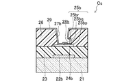
- FIG. 5 is a sectional view taken along line BB in FIG.
- the lower electrode 22b is covered with a gate insulating film 23, an etch stopper layer 24b is disposed on the gate insulating film 23 at a position facing the lower electrode 22b, and an upper portion is formed on the etch stopper layer 24b.
- the electrode 25b is provided, and these constitute the auxiliary capacitance element Cs.
- the lower electrode 22b is formed of a first metal, and has, for example, a configuration in which an aluminum film, a titanium film, and a titanium nitride film are sequentially stacked from the bottom.
- the lower electrode 22b is connected to a storage capacitor terminal TCs provided in the terminal region T.
- the upper electrode 25b is formed of a second metal, and has a configuration in which a first conductive film 25bp, a second conductive film 25bq on the first conductive film 25bp, and a third conductive film 25br on the second conductive film 25bq are sequentially stacked.
- the first conductive film 25bp is made of, for example, a titanium (Ti) film, and has a thickness of, for example, 50 nm.
- the second conductive film 25bq is made of, for example, an aluminum film, and has a thickness of 100 nm, for example.
- the third conductive film 25br is made of a refractory metal film such as a molybdenum nitride (MoN) film, and has a thickness of 150 nm, for example.
- the first conductive film 25bp and the third conductive film 25br are not limited to the above metal film, but the first conductive film 25bp is preferably a refractory metal film.
- the first conductive film 25bp in addition to a titanium (Ti) film, for example, a metal such as a molybdenum (Mo) film, a tantalum (Ta) film, a tungsten (W) film, a chromium (Cr) film, or a nickel (Ni) film. Examples thereof include a film and a metal film made of an alloy of these metals.
- a second contact hole 27 b is provided in the interlayer insulating film 26 and reaches the upper electrode 25 b from the surface of the interlayer insulating film 26.
- the surface of the second contact hole 27b is covered with a pixel electrode 29, and the pixel electrode 29 is electrically connected to the upper electrode 25b.
- the pixel electrode 29 is provided so as to be in contact with the first conductive film 25bp and the third conductive film 25br in the upper electrode 25b. On the other hand, the pixel electrode 29 is not in contact with the second conductive film 25bq of the upper electrode 25b. This is because an air gap 28b is formed between the first conductive film 25bp and the third conductive film 25br so as to communicate with the second contact hole 27b in the wall portion of the second contact hole 27b. This is because the second conductive film 25bq of the electrode 25b and the second contact hole 27b are disposed so as to be separated from each other.
- the gap portion 28b is formed to be a gap having a depth of about 50 to 200 nm from the surface of the second contact hole 27b.
- FIG. 6 is a cross-sectional view taken along the line CC of FIG.
- the terminal 22c is covered with a gate insulating film 23 and an interlayer insulating film 26.
- the terminal 22c is formed of a first metal and has a configuration in which, for example, an aluminum film, a titanium film, and a titanium nitride film are stacked in order from the bottom.
- a third contact hole 27 c is provided in the gate insulating film 23 and the interlayer insulating film 26 so as to reach the terminal 22 c from the surface of the interlayer insulating film 26.
- the surface of the third contact hole 27c is covered with a pixel electrode 29, and the pixel electrode 29 is electrically connected to the terminal 22c to form a gate terminal portion TG .
- Figure 6 shows a cross-section at the gate terminal portion T G, it has the same cross-sectional structure even in the source terminal portion T S.
- Part of the frame region F of the TFT substrate 20 is formed so that the TFT substrate 20 protrudes from the counter substrate 30 and serves as a terminal region T for attaching an external connection terminal (not shown) such as a mounted component.
- transfer pads (not shown) for applying a common potential to the common electrode of the counter substrate 30 are formed, and each transfer pad is connected to a transfer bus line (not shown) arranged in the terminal region T.
- a polarizing plate (not shown) is provided on the surface of the TFT substrate 20 opposite to the liquid crystal layer 50.
- the colored layers of the red colored layer, the green colored layer, and the blue colored layer are arranged on the surface of the substrate body for each pixel.
- a common electrode made of, for example, ITO having a thickness of about 100 nm is provided on each colored layer 22R, G, B, and an alignment film is formed to cover the common electrode.
- Each colored layer is composed of three types of colored layers of red, green and blue.
- the present invention is not limited to this.
- the colored layer is composed of four types of colored layers of red, green, blue and yellow. Also good.
- a polarizing plate (not shown) is provided on the surface of the counter substrate 30 opposite to the liquid crystal layer 50.
- a sealing material 40 is disposed on the outer peripheral edge between the TFT substrate 20 and the counter substrate 30 so as to extend annularly along the frame region F.
- the sealing material 40 bonds the TFT substrate 20 and the counter substrate 30 to each other.
- the sealing material 40 is made by curing a sealing material material mainly composed of an adhesive such as a thermosetting resin or ultraviolet curable resin having fluidity (for example, acrylic resin or epoxy resin) by heating or irradiation with ultraviolet rays. It is a thing.
- conductive beads are mixed in the sealing material 40 and function as a medium for electrically connecting the common electrode and the transfer pad.
- the liquid crystal layer 50 is made of a nematic liquid crystal material having electro-optical characteristics.
- the liquid crystal display device 10 having the above configuration, is configured with one pixel for each pixel electrode, in each pixel, when the gate signal is transmitted from the gate line TFT T R is turned on, the source lines A source signal is sent from the source electrode and a predetermined charge is written to the pixel electrode via the source electrode and the drain electrode, and a potential difference is generated between the pixel electrode and the common electrode of the counter substrate 30. A predetermined voltage is applied to the liquid crystal capacitor. In the liquid crystal display device 10, an image is displayed by adjusting the transmittance of light incident from the outside using the fact that the alignment state of the liquid crystal molecules changes according to the magnitude of the applied voltage.
- the second metal constituting the source electrode 25s, the drain electrode 25d, the upper electrode 25b, etc. of the TFT substrate 20 is the first conductive film 25sp, 25dp, 25bp, the second conductive film 25sq, 25dq, 25bq and the second conductive film.
- the third conductive film 25sr, 25dr, 25br has been described as having a configuration in which the third conductive film 25sr, 25dr, 25br are sequentially stacked. 2 conductive layers 25sq, 25dq, and 25bq may be stacked).
- the manufacturing method of the TFT substrate 20 of this embodiment includes a thin film transistor forming step, an interlayer insulating film forming step, a first etching step, a second etching step, and a pixel electrode forming step.
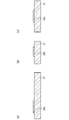
- a first metal is provided on the substrate 21, and as shown in FIGS. 7A to 7C, a gate electrode 22a, a lower electrode 22b, a terminal 22c, a gate line 22gb (see FIG. 3), a transfer pad (not shown) Etc.).
- a portion that becomes a gate electrode 22a, a lower electrode 22b, a terminal 22c, and the like by using a photolithography method after an aluminum film, a titanium film, and a titanium nitride film are successively stacked using, for example, a sputtering method.
- the resist pattern is left on.
- the resist is stripped with a resist stripping solution.
- RIE method dry etching method
- a SiO 2 film is formed as the gate insulating film 23 by using, for example, a CVD method.
- an oxide semiconductor film 24a and an etch stopper layer 24b are formed.
- an oxide semiconductor film such as an IGZO film is formed using a sputtering method or the like, and then a resist pattern is formed on portions to be the oxide semiconductor film 24a and the etch stopper layer 24b using a photolithography method. Remain.
- the IGZO film is etched by a wet etching method using an oxalic acid solution as an etchant, the resist is stripped with a resist stripper.
- a source electrode 25s, a drain electrode 25d, and an upper electrode 25b are formed.
- a titanium film (thickness of about 50 nm) that becomes the first conductive films 25sp, 25dp, and 25bp, an aluminum film (thickness of about 150 nm) that becomes the second conductive films 25sq, 25dq, and 25bq, and a third conductive film Molybdenum nitride films (thickness of about 100 nm) to be the films 25sr, 25dr, and 25br are continuously stacked using, for example, a sputtering method, and then the source electrode 25s, the drain electrode 25d, and the upper electrode 25b are formed using a photolithography method.
- the resist pattern is left in the part to be.
- the second conductive film and the third conductive film are etched by wet etching using a mixed acid solution of phosphoric acid / acetic acid / nitric acid as an etching solution, and further dry etching (RIE method) using a chlorine-based gas is performed.
- RIE method dry etching
- the resist is stripped with a resist stripping solution.
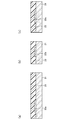
- an SiO 2 film is formed as the interlayer insulating film 26 by using, for example, a CVD method.
- the interlayer insulating film 26 is dry-etched to form a first contact hole 27a, a second contact hole 27b, and a third contact hole 27c, as shown in FIGS.
- a photosensitive resist is applied on the interlayer insulating film 26, and then the resist is left in portions other than the portions to be the first to third contact holes 27a to 27c by using a photolithography method.
- a photolithography method for example, an interlayer insulating film using a dry etching method (RIE method) using a fluorine-based gas such as sulfur hexafluoride (SF 6 ), carbon tetrafluoride (CF 4 ), or trifluoromethane (CHF 3 ).
- RIE method dry etching method
- fluorine-based gas such as sulfur hexafluoride (SF 6 ), carbon tetrafluoride (CF 4 ), or trifluoromethane (CHF 3 ).
- the third conductive film 25dr constituting the outermost layer of the drain electrode 25d is also etched.
- the first contact hole 27a is provided in a region including the boundary between the drain electrode 25d and the oxide semiconductor film 24a. That is, both the drain electrode 25d and the oxide semiconductor film 24a are exposed on the surface of the first contact hole 27a.
- the oxide semiconductor film 24a functions as an etching stopper because the oxide semiconductor film 25a is provided in a portion where the drain electrode 25d does not exist in a region to be the first contact hole 27a.
- the etch stopper layer 24b functions as an etching stopper.
- the interlayer insulating film 26 and the third conductive films 25dr and 25br are removed by etching to form the first and second contact holes 27a and 27b, so that the surfaces of the first and second contact holes 27a and 27b are formed.
- the second conductive films 25dq and 25bq are exposed, but the exposed surfaces of the second conductive films 25dq and 25bq are each fluorinated with a fluorine-based gas, and a high resistance film of aluminum fluoride is formed on the surface. It is formed.
- the resist is removed by oxygen ashing.
- the second conductive films 25dq and 25bq exposed on the surfaces of the first and second contact holes 27a and 27b shown in FIGS. 12A and 12B are made of aluminum fluoride. Is oxidized by oxygen ashing to form an aluminum oxide film containing fluorine, that is, a passive film.
- the third contact hole 27c is formed in the gate terminal portion TG .
- both the interlayer insulating film 26 and the gate insulating film 23 are removed, and the terminal 22c is Functions as an etch stopper.
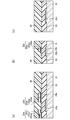
- etching process (Second etching process) Subsequent to the first etching step, wet etching is performed as shown in FIGS. At this time, for example, an etchant having a high selectivity of aluminum to an oxide semiconductor is used. This makes it possible to selectively etch only the second conductive films 25dq and 25bq made of an aluminum film among the structures exposed on the surfaces of the first contact hole 27a and the second contact hole 27b. Thereby, the space
- the selectivity of aluminum to the oxide semiconductor is preferably 5 or more. Examples of such an etchant include ammonia water having a selectivity ratio of aluminum to an oxide semiconductor of 20 or more.
- an ITO film is formed using, for example, a sputtering method, and then a resist pattern is left in a portion that becomes the pixel electrode 29 using a photolithography method. Then, for example, the pixel electrode is formed by etching the ITO film using an oxalic acid solution as an etchant and stripping the resist with a resist stripper.
- the pixel electrode 29 is provided so as to contact the first conductive film 25dp and third conductive 25dr the drain electrode 25d.
- the pixel electrode 29 and the third conductive film 25dq are not in contact with each other.
- the auxiliary capacitance element Cs as shown in FIG. 14B, the pixel electrode 29 is provided in contact with the first conductive film 25bp and the third conductive film 25br of the upper electrode 25b.
- the pixel electrode 29 and the third conductive film 25bq are not in contact with each other.
- the gate terminal portion TG as shown in FIG. 14C, the pixel electrode 29 is provided so as to be electrically connected to the terminal 22c.
- the TFT substrate 20 is manufactured.
- the second conductive films 25dq and 25bq are respectively formed in the second etching process.
- the first conductive film 25dp and 25bp and the third conductive film 25dr and 25br are formed in the wall portion of the first contact hole 27a and the second contact hole 27b so as to be separated from the first contact hole 27a and the second contact hole 27b. Since the gaps 28a and 28b are formed, the high resistance film and the passive film formed in the first etching process are removed in the second etching process.
- the drain electrode 25d in the first conductive film 25dp and portions of the third conductive film 25dr other than the second conductive film 25dq
- the pixel electrode 29 and the drain electrode 25d are electrically connected. Therefore, a good contact between the pixel electrode 29 and the drain electrode 25d can be obtained without causing a contact failure between the pixel electrode 29 and the drain electrode 25d due to the presence of the high resistance film or the passive film on the surface of the drain electrode 25d. It is done.
- the pixel electrode 29 formed in the pixel electrode formation step is a portion of the first conductive film 25bp and the third conductive film 25br other than the second conductive film 25bq, from the upper electrode 25b.
- the pixel electrode 29 and the upper electrode 25b are electrically connected. Therefore, a good contact between the pixel electrode 29 and the upper electrode 25b can be obtained without causing a contact failure between the pixel electrode 29 and the upper electrode 25b due to the presence of the high resistance film or the passive film on the surface of the upper electrode 25b. It is done.
- the TFT substrate 20 prepared by the above method and the counter substrate 30 on which a color filter is formed for each pixel are arranged to face each other and bonded together with a sealing material 40, and a liquid crystal material is filled between the substrates to fill the liquid crystal.
- the layer 50 the liquid crystal display device 10 can be obtained.
- the resist is removed by oxygen ashing in the first etching step.
- the present invention is not limited to this.
- the resist may be removed using a resist stripping solution or the like.
- the aluminum film is not oxidized and the surfaces of the second conductive films 25dq and 25bp are not covered with the aluminum oxide film, that is, the passive film.
- the surfaces of the second conductive films 25dq and 25bp are covered with a high resistance film of aluminum fluoride, so that there is a problem that contact failure occurs even if the second conductive films 25dq and 25bp contact the pixel electrode 29.
- the second conductive films 25dq and 25bq are respectively formed in the second etching step.
- the first conductive film 25dp and 25bp and the third conductive film 25dr and 25br are respectively formed in the second etching step.
- the high resistance film formed in the first etching process is removed in the second etching process. Therefore, a good contact can be obtained without causing a contact failure between the pixel electrode 29 and the drain electrode 25d or the upper electrode 25b due to the presence of the high resistance film on the surface of the drain electrode 25d.
- the present invention is useful for a thin film transistor substrate, a liquid crystal display device including the same, and a thin film transistor substrate.
- TFT substrate 21 substrate 22a gate electrode 22b lower electrode 23 gate insulating film 24a oxide semiconductor film 24ac channel portion 24b etch stopper layer 25a oxide semiconductor film 25b upper electrode 25d drain electrode 25dp, 25bp first conductive film 25dq, 25bq second conductive film 25dr , 25br third conductive film 25s source electrode 26 interlayer insulating film 27a first contact hole 27b second contact hole 28a, 28b gap 29 pixel electrode 30 counter substrate 40 sealing material 50 liquid crystal layer
Landscapes
- Physics & Mathematics (AREA)
- Nonlinear Science (AREA)
- Engineering & Computer Science (AREA)
- Mathematical Physics (AREA)
- Chemical & Material Sciences (AREA)
- Crystallography & Structural Chemistry (AREA)
- Microelectronics & Electronic Packaging (AREA)
- General Physics & Mathematics (AREA)
- Optics & Photonics (AREA)
- Power Engineering (AREA)
- Thin Film Transistor (AREA)
- Liquid Crystal (AREA)
- Internal Circuitry In Semiconductor Integrated Circuit Devices (AREA)
Abstract
Description
基板上に設けられたゲート電極、ゲート電極を覆うように設けられたゲート絶縁膜、ゲート絶縁膜の上層に設けられゲート電極に対向する位置にチャネル部を有する酸化物半導体膜、並びに、酸化物半導体膜上にチャネル部を介して互いに離間して設けられたソース電極及びドレイン電極を有する薄膜トランジスタと、
ゲート絶縁膜の上層に薄膜トランジスタを覆うように設けられ、ドレイン電極に達する第1コンタクトホールを有する層間絶縁膜と、
層間絶縁膜上に設けられ、第1コンタクトホールを介してドレイン電極に電気的に接続された画素電極と、
を備えたものであって、
ドレイン電極は、第1導電膜と、第1導電膜の上層に設けられアルミニウムからなる第2導電膜と、が積層された構成を有し、第2導電膜が第1コンタクトホールと離間することにより両者間に第1コンタクトホールと連通する空隙部が形成され、
画素電極は、ドレイン電極のうち第2導電膜とは接触しないように設けられていることを特徴とする。
補助容量素子は、エッチストッパ層及び上部電極に達する第2コンタクトホールをさらに有する層間絶縁膜に覆われており、
上部電極は、第1導電膜と、第1導電膜の上層に設けられアルミニウムからなる第2導電膜と、が積層された構成を有し、第2導電膜が第2コンタクトホールと離間することにより両者間に第2コンタクトホールと連通する空隙部が形成され、
第2コンタクトホール表面には、上部電極のうち第2導電膜とは接触しないで上部電極と電気的に接続されるように画素電極が設けられていることが好ましい。
上部電極は、第1導電膜及び第2導電膜に加え、さらに、第2導電膜の上層に第3導電膜が設けられた構成を有していてもよい。
薄膜トランジスタ基板に対向配置された対向基板と、
薄膜トランジスタ基板と対向基板との間に設けられた液晶層と、
を備えた液晶表示装置に好適に用いられる。
薄膜トランジスタ形成工程で形成した薄膜トランジスタを覆うようにゲート絶縁膜の上層に層間絶縁膜を形成する層間絶縁膜形成工程と、
層間絶縁膜形成工程の後、層間絶縁膜に対してドライエッチングを行って、第2導電膜が表面に露出するように層間絶縁膜からドレイン電極に達する第1コンタクトホールを形成する第1エッチング工程と、
第1エッチング工程で形成した第1コンタクトホールに対して、アルミニウムの酸化物半導体に対する選択比が高いエッチング液を用いたウェットエッチングを行って、第2導電膜を第1コンタクトホールと離間させることにより両者間に第1コンタクトホールに連通する空隙部を形成する第2エッチング工程と、
第2エッチング工程において空隙部が設けられた層間絶縁膜の表面及び第1コンタクトホールの表面を含む領域に導電膜を成膜して、ドレイン電極のうち第2導電膜とは接触しないでドレイン電極と電気的に接続されるように画素電極を形成する画素電極形成工程と、
を備えたことを特徴とする。
図1及び2は、本実施形態にかかる液晶表示装置10を示す。液晶表示装置10は、互いに対向して配置されたTFT基板20及び対向基板30を備えている。両基板20及び30は、それらの外周縁部に枠状に配置されたシール材40により接着されている。そして、両基板20及び30の間のシール材40に包囲された空間には、表示層として液晶層50が設けられている。液晶表示装置10は、シール材40の内側に形成されて複数の画素がマトリクス状に配置された表示領域Dを有し、それを囲む領域が額縁領域Fとなっている。
図3は、TFT基板20の平面図である。TFT基板20は、ガラス基板等からなる基板21上に、ゲート電極22a、下部電極22b、端子22cやゲート線22gb、トランスファパッド(不図示)等を含む第1メタル、SiO2やSiO2とSiNとの積層体等からなるゲート絶縁膜23、IGZO膜等からなる酸化物半導体膜24a~b、ソース電極25s、ドレイン電極25d、上部電極25bやソース線25sb等を含む第2メタル、SiO2、SiN、透明絶縁性樹脂等からなる層間絶縁膜26、ITO(Indium Tin Oxide)膜等からなる画素電極29、及びポリイミド膜等からなる配向膜(不図示)が積層形成されている。
対向基板30は、図示しないが、表示領域Dにおいて、基板本体表面に、赤色着色層、緑色着色層、及び青色着色層の各着色層が画素毎に配されている。そして、各着色層22R,G,Bの上層には、例えば厚さ100nm程度のITO等からなる共通電極が設けられ、さらに、共通電極を覆うように配向膜が形成されている。なお、各着色層が赤色、緑色及び青色の3種類の着色層で構成されるとしたが、これに限られず、例えば、赤色、緑色、青色及び黄色の4種類の着色層で構成されていてもよい。
TFT基板20と対向基板30の間の外周縁部には、額縁領域Fに沿って環状に延びるようにシール材40が配置されている。そして、シール材40がTFT基板20と対向基板30とを互いに接着している。
液晶層50は、電気光学特性を有するネマチック液晶材料などにより構成されている。
以下、本実施形態のTFT基板20を製造する方法について説明する。本実施形態のTFT基板20の製造方法は、薄膜トランジスタ形成工程、層間絶縁膜形成工程、第1エッチング工程、第2エッチング工程、及び画素電極形成工程を備えている。
まず、基板21上に第1メタルを設け、図7(a)~(c)に示すように、ゲート電極22a、下部電極22b、端子22c、ゲート線22gb(図3参照)、トランスファパッド(不図示)等を形成する。具体的には、アルミニウム膜、チタン膜、及び窒化チタン膜を例えばスパッタ法を用いて連続して積層形成した後、フォトリソグラフィ法を用いてゲート電極22a、下部電極22b、端子22c等となる部分にレジストパターンを残存させる。そして、例えば、塩素系のガスを用いたドライエッチング法(RIE法)を用いてアルミニウム膜、チタン膜、及び窒化チタン膜の導電膜の積層体をエッチングした後、レジスト剥離液にてレジストを剥離する。
次に、図11(a)~(c)に示すように、層間絶縁膜26として、例えばCVD法を用いてSiO2膜を形成する。
次いで、層間絶縁膜26をドライエッチングすることにより、図12(a)~(c)に示すように、第1コンタクトホール27a,第2コンタクトホール27b,第3コンタクトホール27cを形成する。
第1エッチング工程に続いて、図13(a)及び(b)に示すように、ウェットエッチングを行う。このとき、エッチング液としては、例えば、アルミニウムの酸化物半導体に対する選択比が高いものを使用する。これにより、第1コンタクトホール27aや第2コンタクトホール27bの表面に露出した構成のうち、アルミニウム膜からなる第2導電膜25dq、25bqだけを選択的にエッチングすることが可能となる。これにより、空隙部28a,28bが形成される。アルミニウムの酸化物半導体に対する選択比としては、5以上であることが好ましい。かかるエッチング液としては、例えば、アルミニウムの酸化物半導体に対する選択比が20以上のアンモニア水等が挙げられる。
最後に、図14(a)~(c)に示すように、画素電極29を形成する。
TR 薄膜トランジスタ
10 液晶表示装置
20 薄膜トランジスタ基板(TFT基板)
21 基板
22a ゲート電極
22b 下部電極
23 ゲート絶縁膜
24a 酸化物半導体膜
24ac チャネル部
24b エッチストッパ層
25a 酸化物半導体膜
25b 上部電極
25d ドレイン電極
25dp、25bp 第1導電膜
25dq、25bq 第2導電膜
25dr、25br 第3導電膜
25s ソース電極
26 層間絶縁膜
27a 第1コンタクトホール
27b 第2コンタクトホール
28a,28b 空隙部
29 画素電極
30 対向基板
40 シール材
50 液晶層
Claims (8)
- 基板と、
上記基板上に設けられたゲート電極、該ゲート電極を覆うように設けられたゲート絶縁膜、該ゲート絶縁膜の上層に設けられ上記ゲート電極に対向する位置にチャネル部を有する酸化物半導体膜、並びに、該酸化物半導体膜上に上記チャネル部を介して互いに離間して設けられたソース電極及びドレイン電極を有する薄膜トランジスタと、
上記ゲート絶縁膜の上層に上記薄膜トランジスタを覆うように設けられ、上記ドレイン電極に達する第1コンタクトホールを有する層間絶縁膜と、
上記層間絶縁膜上に設けられ、上記第1コンタクトホールを介して上記ドレイン電極に電気的に接続された画素電極と、
を備えた薄膜トランジスタ基板であって、
上記ドレイン電極は、第1導電膜と、該第1導電膜の上層に設けられアルミニウムからなる第2導電膜と、が積層された構成を有し、上記第2導電膜が上記第1コンタクトホールと離間することにより両者間に該第1コンタクトホールと連通する空隙部が形成され、
上記画素電極は、上記ドレイン電極のうち上記第2導電膜とは接触しないように設けられている
ことを特徴とする薄膜トランジスタ基板。 - 請求項1に記載された薄膜トランジスタ基板において、
上記基板上に上記ゲート電極と同一層に設けられた下部電極、該ゲート電極及び該下部電極を覆うように設けられた上記ゲート絶縁膜、該ゲート絶縁膜の上層の上記下部電極に対向する位置に設けられ酸化物半導体からなるエッチストッパ層、及び、該エッチストッパ層上に上記ドレイン電極と同一層に設けられた上部電極を有する補助容量素子をさらに備え、
上記補助容量素子は、上記エッチストッパ層及び上記上部電極に達する第2コンタクトホールをさらに有する上記層間絶縁膜に覆われており、
上記上部電極は、第1導電膜と、該第1導電膜の上層に設けられアルミニウムからなる第2導電膜と、が積層された構成を有し、上記第2導電膜が上記第2コンタクトホールと離間することにより両者間に該第2コンタクトホールと連通する空隙部が形成され、
上記第2コンタクトホール表面には、上記上部電極のうち上記第2導電膜とは接触しないで該上部電極と電気的に接続されるように上記画素電極が設けられている
ことを特徴とする薄膜トランジスタ基板。 - 請求項1または2に記載された薄膜トランジスタ基板において、
上記第1導電膜は高融点金属膜で形成される
ことを特徴とする薄膜トランジスタ基板。 - 請求項1に記載された薄膜トランジスタ基板において、
上記ドレイン電極は、上記第1導電膜及び第2導電膜に加え、さらに、該第2導電膜の上層に第3導電膜が設けられた構成を有する
ことを特徴とする薄膜トランジスタ基板。 - 請求項2に記載された薄膜トランジスタ基板において、
上記ドレイン電極は、上記第1導電膜及び第2導電膜に加え、さらに、該第2導電膜の上層に第3導電膜が設けられた構成を有し、
上記上部電極は、上記第1導電膜及び第2導電膜に加え、さらに、該第2導電膜の上層に第3導電膜が設けられた構成を有する
ことを特徴とする薄膜トランジスタ基板。 - 請求項1~5のいずれかに記載された薄膜トランジスタ基板と、
上記薄膜トランジスタ基板に対向配置された対向基板と、
上記薄膜トランジスタ基板と上記対向基板との間に設けられた液晶層と、
を備えたことを特徴とする液晶表示装置。 - 請求項1に記載された薄膜トランジスタ基板の製造方法であって、
基板上に設けられたゲート電極、該ゲート電極を覆うように設けられたゲート絶縁膜、該ゲート絶縁膜の上層に設けられ該ゲート電極に対向する位置にチャネル部を有する酸化物半導体膜、並びに、該酸化物半導体膜上に該チャネル部を介して互いに離間するように、第1導電膜、及びその上層の第2導電膜が積層して設けられたソース電極及びドレイン電極を有する薄膜トランジスタを形成する薄膜トランジスタ形成工程と、
上記薄膜トランジスタ形成工程で形成した薄膜トランジスタを覆うように上記ゲート絶縁膜の上層に層間絶縁膜を形成する層間絶縁膜形成工程と、
上記層間絶縁膜形成工程の後、上記層間絶縁膜に対してドライエッチングを行って、上記第2導電膜が表面に露出するように上記層間絶縁膜から上記ドレイン電極に達する第1コンタクトホールを形成する第1エッチング工程と、
上記第1エッチング工程で形成した上記第1コンタクトホールに対して、アルミニウムの酸化物半導体に対する選択比が高いエッチング液を用いたウェットエッチングを行って、該第2導電膜を上記第2コンタクトホールと離間させることにより両者間に該第1コンタクトホールに連通する空隙部を形成する第2エッチング工程と、
上記第2エッチング工程において上記空隙部が設けられた上記層間絶縁膜の表面及び上記第1コンタクトホールの表面を含む領域に導電膜を成膜して、上記ドレイン電極のうち上記第2導電膜とは接触しないで該ドレイン電極と電気的に接続されるように画素電極を形成する画素電極形成工程と、
を備えたことを特徴とする薄膜トランジスタ基板の製造方法。 - 請求項7に記載された薄膜トランジスタ基板の製造方法において、
上記第2エッチング工程で用いるエッチング液は、アンモニア水であることを特徴とする薄膜トランジスタ基板の製造方法。
Priority Applications (4)
| Application Number | Priority Date | Filing Date | Title |
|---|---|---|---|
| JP2012527566A JP5269254B2 (ja) | 2010-08-03 | 2011-05-26 | 薄膜トランジスタ基板 |
| US13/813,703 US20130208205A1 (en) | 2010-08-03 | 2011-05-26 | Thin film transistor substrate |
| CN2011800379690A CN103053027A (zh) | 2010-08-03 | 2011-05-26 | 薄膜晶体管基板 |
| KR1020137003957A KR101318595B1 (ko) | 2010-08-03 | 2011-05-26 | 박막 트랜지스터 기판 |
Applications Claiming Priority (2)
| Application Number | Priority Date | Filing Date | Title |
|---|---|---|---|
| JP2010-174792 | 2010-08-03 | ||
| JP2010174792 | 2010-08-03 |
Publications (1)
| Publication Number | Publication Date |
|---|---|
| WO2012017584A1 true WO2012017584A1 (ja) | 2012-02-09 |
Family
ID=45559110
Family Applications (1)
| Application Number | Title | Priority Date | Filing Date |
|---|---|---|---|
| PCT/JP2011/002931 Ceased WO2012017584A1 (ja) | 2010-08-03 | 2011-05-26 | 薄膜トランジスタ基板 |
Country Status (5)
| Country | Link |
|---|---|
| US (1) | US20130208205A1 (ja) |
| JP (1) | JP5269254B2 (ja) |
| KR (1) | KR101318595B1 (ja) |
| CN (1) | CN103053027A (ja) |
| WO (1) | WO2012017584A1 (ja) |
Cited By (4)
| Publication number | Priority date | Publication date | Assignee | Title |
|---|---|---|---|---|
| WO2015079360A1 (en) * | 2013-11-29 | 2015-06-04 | Semiconductor Energy Laboratory Co., Ltd. | Semiconductor device, method for manufacturing the same, and display device |
| WO2016039211A1 (ja) * | 2014-09-10 | 2016-03-17 | シャープ株式会社 | 半導体装置、液晶表示装置および半導体装置の製造方法 |
| JP2020113615A (ja) * | 2019-01-10 | 2020-07-27 | 株式会社ジャパンディスプレイ | 配線構造体、半導体装置、及び表示装置 |
| JP2025093986A (ja) * | 2013-06-21 | 2025-06-24 | 株式会社半導体エネルギー研究所 | 表示装置 |
Families Citing this family (7)
| Publication number | Priority date | Publication date | Assignee | Title |
|---|---|---|---|---|
| JP6563194B2 (ja) * | 2012-11-05 | 2019-08-21 | ソニーセミコンダクタソリューションズ株式会社 | 光学装置の製造方法 |
| US9991392B2 (en) | 2013-12-03 | 2018-06-05 | Semiconductor Energy Laboratory Co., Ltd. | Semiconductor device and manufacturing method thereof |
| KR102235443B1 (ko) | 2014-01-10 | 2021-04-02 | 삼성디스플레이 주식회사 | 박막 트랜지스터 표시판 및 그 제조 방법 |
| KR102717808B1 (ko) * | 2016-11-30 | 2024-10-15 | 엘지디스플레이 주식회사 | 두 개의 전극들 사이에 위치하는 다수의 절연막들을 포함하는 디스플레이 장치 |
| CN110676264B (zh) * | 2019-09-09 | 2021-11-23 | Tcl华星光电技术有限公司 | 像素电极接触孔设计 |
| CN110941126B (zh) * | 2019-12-27 | 2021-04-27 | Tcl华星光电技术有限公司 | 阵列基板及其制作方法 |
| TWI752508B (zh) * | 2020-05-26 | 2022-01-11 | 群創光電股份有限公司 | 顯示裝置 |
Citations (8)
| Publication number | Priority date | Publication date | Assignee | Title |
|---|---|---|---|---|
| JPH11312810A (ja) * | 1998-04-28 | 1999-11-09 | Matsushita Electric Ind Co Ltd | 反射型液晶表示装置およびその製造方法 |
| JP2000196092A (ja) * | 1998-12-25 | 2000-07-14 | Fujitsu Ltd | 積層金属配線及び薄膜トランジスタ基板、並びにそれらの製造方法 |
| JP2001042361A (ja) * | 1999-08-04 | 2001-02-16 | Sharp Corp | 透過型液晶表示装置 |
| JP2002324904A (ja) * | 2001-04-24 | 2002-11-08 | Matsushita Electric Ind Co Ltd | 薄膜トランジスタ及びその形成方法 |
| JP2006201781A (ja) * | 2005-01-18 | 2006-08-03 | Samsung Electronics Co Ltd | 薄膜トランジスタ表示板及び薄膜トランジスタ表示板の製造方法 |
| WO2007097078A1 (ja) * | 2006-02-24 | 2007-08-30 | Sharp Kabushiki Kaisha | アクティブマトリクス基板、表示装置、テレビジョン受像機 |
| WO2009066750A1 (ja) * | 2007-11-22 | 2009-05-28 | Idemitsu Kosan Co., Ltd. | エッチング液組成物 |
| JP2010135773A (ja) * | 2008-11-07 | 2010-06-17 | Semiconductor Energy Lab Co Ltd | 半導体装置及び半導体装置の作製方法 |
Family Cites Families (2)
| Publication number | Priority date | Publication date | Assignee | Title |
|---|---|---|---|---|
| KR100766493B1 (ko) * | 2001-02-12 | 2007-10-15 | 삼성전자주식회사 | 박막트랜지스터 액정표시장치 |
| US7023016B2 (en) * | 2003-07-02 | 2006-04-04 | Samsung Electronics Co., Ltd. | Thin film transistor array panel and manufacturing method thereof |
-
2011
- 2011-05-26 WO PCT/JP2011/002931 patent/WO2012017584A1/ja not_active Ceased
- 2011-05-26 KR KR1020137003957A patent/KR101318595B1/ko not_active Expired - Fee Related
- 2011-05-26 US US13/813,703 patent/US20130208205A1/en not_active Abandoned
- 2011-05-26 JP JP2012527566A patent/JP5269254B2/ja active Active
- 2011-05-26 CN CN2011800379690A patent/CN103053027A/zh active Pending
Patent Citations (8)
| Publication number | Priority date | Publication date | Assignee | Title |
|---|---|---|---|---|
| JPH11312810A (ja) * | 1998-04-28 | 1999-11-09 | Matsushita Electric Ind Co Ltd | 反射型液晶表示装置およびその製造方法 |
| JP2000196092A (ja) * | 1998-12-25 | 2000-07-14 | Fujitsu Ltd | 積層金属配線及び薄膜トランジスタ基板、並びにそれらの製造方法 |
| JP2001042361A (ja) * | 1999-08-04 | 2001-02-16 | Sharp Corp | 透過型液晶表示装置 |
| JP2002324904A (ja) * | 2001-04-24 | 2002-11-08 | Matsushita Electric Ind Co Ltd | 薄膜トランジスタ及びその形成方法 |
| JP2006201781A (ja) * | 2005-01-18 | 2006-08-03 | Samsung Electronics Co Ltd | 薄膜トランジスタ表示板及び薄膜トランジスタ表示板の製造方法 |
| WO2007097078A1 (ja) * | 2006-02-24 | 2007-08-30 | Sharp Kabushiki Kaisha | アクティブマトリクス基板、表示装置、テレビジョン受像機 |
| WO2009066750A1 (ja) * | 2007-11-22 | 2009-05-28 | Idemitsu Kosan Co., Ltd. | エッチング液組成物 |
| JP2010135773A (ja) * | 2008-11-07 | 2010-06-17 | Semiconductor Energy Lab Co Ltd | 半導体装置及び半導体装置の作製方法 |
Cited By (7)
| Publication number | Priority date | Publication date | Assignee | Title |
|---|---|---|---|---|
| JP2025093986A (ja) * | 2013-06-21 | 2025-06-24 | 株式会社半導体エネルギー研究所 | 表示装置 |
| JP7829766B2 (ja) | 2013-06-21 | 2026-03-13 | 株式会社半導体エネルギー研究所 | 表示装置 |
| WO2015079360A1 (en) * | 2013-11-29 | 2015-06-04 | Semiconductor Energy Laboratory Co., Ltd. | Semiconductor device, method for manufacturing the same, and display device |
| WO2016039211A1 (ja) * | 2014-09-10 | 2016-03-17 | シャープ株式会社 | 半導体装置、液晶表示装置および半導体装置の製造方法 |
| US10073314B2 (en) | 2014-09-10 | 2018-09-11 | Sharp Kabushiki Kaisha | Semiconductor device, liquid crystal display device, and semiconductor device manufacturing method |
| JP2020113615A (ja) * | 2019-01-10 | 2020-07-27 | 株式会社ジャパンディスプレイ | 配線構造体、半導体装置、及び表示装置 |
| JP7263013B2 (ja) | 2019-01-10 | 2023-04-24 | 株式会社ジャパンディスプレイ | 配線構造体、半導体装置、及び表示装置 |
Also Published As
| Publication number | Publication date |
|---|---|
| JP5269254B2 (ja) | 2013-08-21 |
| JPWO2012017584A1 (ja) | 2013-09-19 |
| CN103053027A (zh) | 2013-04-17 |
| US20130208205A1 (en) | 2013-08-15 |
| KR20130069731A (ko) | 2013-06-26 |
| KR101318595B1 (ko) | 2013-10-15 |
Similar Documents
| Publication | Publication Date | Title |
|---|---|---|
| JP5269254B2 (ja) | 薄膜トランジスタ基板 | |
| JP5330603B2 (ja) | 薄膜トランジスタ基板及びそれを備えた液晶表示装置 | |
| JP5275519B2 (ja) | 表示装置用基板及びその製造方法、表示装置 | |
| JP3980156B2 (ja) | アクティブマトリクス型表示装置 | |
| KR102127781B1 (ko) | 박막 트랜지스터 어레이 기판 및 그 제조 방법 | |
| CN102884632A (zh) | 薄膜晶体管、接触结构、基板、显示装置和它们的制造方法 | |
| JP5505757B2 (ja) | 液晶表示装置の製造方法および液晶表示装置 | |
| WO2009081633A1 (ja) | アクティブマトリクス基板、これを備えた液晶表示装置、及びアクティブマトリクス基板の製造方法 | |
| JP5120828B2 (ja) | 薄膜トランジスタ基板とその製造方法、及びこれを有する液晶表示パネルとその製造方法 | |
| US6806933B2 (en) | Array substrate with multi-layer electrode line | |
| WO2012176702A1 (ja) | Tft基板およびその製造方法ならびに表示装置 | |
| JP5900823B2 (ja) | 液晶表示装置 | |
| US8698153B2 (en) | Semiconductor device and process for production thereof | |
| JPWO2007039954A1 (ja) | 薄膜トランジスタアレイ基板の製造方法、及び薄膜トランジスタアレイ基板 | |
| CN101082749A (zh) | 液晶显示装置及其制造方法 | |
| JP4628393B2 (ja) | アクティブマトリクス型液晶表示装置の作製方法 | |
| JP2010231233A (ja) | 液晶表示装置用基板及びそれを用いた液晶表示装置 | |
| JP2007193373A (ja) | 液晶表示装置用基板及びそれを用いた液晶表示装置 | |
| WO2013076940A1 (ja) | アクティブマトリクス基板及び液晶表示装置 | |
| JP3803640B2 (ja) | 液晶表示装置 | |
| WO1996030801A1 (en) | Liquid crystal display | |
| JP2008242086A (ja) | 電気光学装置製造方法 | |
| JP2001147449A (ja) | 液晶画像表示装置と画像表示装置用半導体装置の製造方法 | |
| JP2010008766A (ja) | 表示装置及びその製造方法 | |
| JP2011107352A (ja) | 画像表示装置及びその製造方法 |
Legal Events
| Date | Code | Title | Description |
|---|---|---|---|
| WWE | Wipo information: entry into national phase |
Ref document number: 201180037969.0 Country of ref document: CN |
|
| 121 | Ep: the epo has been informed by wipo that ep was designated in this application |
Ref document number: 11814224 Country of ref document: EP Kind code of ref document: A1 |
|
| WWE | Wipo information: entry into national phase |
Ref document number: 2012527566 Country of ref document: JP |
|
| NENP | Non-entry into the national phase |
Ref country code: DE |
|
| ENP | Entry into the national phase |
Ref document number: 20137003957 Country of ref document: KR Kind code of ref document: A |
|
| WWE | Wipo information: entry into national phase |
Ref document number: 13813703 Country of ref document: US |
|
| 122 | Ep: pct application non-entry in european phase |
Ref document number: 11814224 Country of ref document: EP Kind code of ref document: A1 |