WO2012017491A1 - Light-emitting element, light-emitting device provided with light-emitting element, and light-emitting element production method - Google Patents
Light-emitting element, light-emitting device provided with light-emitting element, and light-emitting element production method Download PDFInfo
- Publication number
- WO2012017491A1 WO2012017491A1 PCT/JP2010/004962 JP2010004962W WO2012017491A1 WO 2012017491 A1 WO2012017491 A1 WO 2012017491A1 JP 2010004962 W JP2010004962 W JP 2010004962W WO 2012017491 A1 WO2012017491 A1 WO 2012017491A1
- Authority
- WO
- WIPO (PCT)
- Prior art keywords
- bank
- layer
- injection layer
- charge injection
- light emitting
- Prior art date
Links
Images

Classifications
-
- H—ELECTRICITY
- H10—SEMICONDUCTOR DEVICES; ELECTRIC SOLID-STATE DEVICES NOT OTHERWISE PROVIDED FOR
- H10K—ORGANIC ELECTRIC SOLID-STATE DEVICES
- H10K50/00—Organic light-emitting devices
- H10K50/10—OLEDs or polymer light-emitting diodes [PLED]
- H10K50/17—Carrier injection layers
-
- H—ELECTRICITY
- H10—SEMICONDUCTOR DEVICES; ELECTRIC SOLID-STATE DEVICES NOT OTHERWISE PROVIDED FOR
- H10K—ORGANIC ELECTRIC SOLID-STATE DEVICES
- H10K59/00—Integrated devices, or assemblies of multiple devices, comprising at least one organic light-emitting element covered by group H10K50/00
- H10K59/10—OLED displays
- H10K59/12—Active-matrix OLED [AMOLED] displays
- H10K59/122—Pixel-defining structures or layers, e.g. banks
-
- H—ELECTRICITY
- H10—SEMICONDUCTOR DEVICES; ELECTRIC SOLID-STATE DEVICES NOT OTHERWISE PROVIDED FOR
- H10K—ORGANIC ELECTRIC SOLID-STATE DEVICES
- H10K71/00—Manufacture or treatment specially adapted for the organic devices covered by this subclass
-
- H—ELECTRICITY
- H10—SEMICONDUCTOR DEVICES; ELECTRIC SOLID-STATE DEVICES NOT OTHERWISE PROVIDED FOR
- H10K—ORGANIC ELECTRIC SOLID-STATE DEVICES
- H10K50/00—Organic light-emitting devices
- H10K50/80—Constructional details
- H10K50/805—Electrodes
- H10K50/81—Anodes
- H10K50/818—Reflective anodes, e.g. ITO combined with thick metallic layers
Definitions
- the present invention relates to a light emitting element, a light emitting device including the light emitting element, and a method for manufacturing the light emitting element.
- organic electroluminescence element (hereinafter referred to as an “organic EL element”), which has been researched and developed in recent years, is a light-emitting element utilizing an electroluminescence phenomenon of an organic material.
- the organic EL element has a structure in which a light emitting layer is interposed between a first electrode (anode) and a second electrode (cathode).
- a bank made of an insulating material is formed on the side of the light emitting layer, and the shape of the light emitting layer is defined by this bank.
- a hole injection layer is interposed between the first electrode and the light emitting layer, if necessary, and an electron injection layer is interposed between the second electrode and the light emitting layer, if necessary (
- the hole injection layer and the electron injection layer are collectively referred to as “charge injection layer”).
- a charge injection layer is formed using a conductive polymer material such as PEDOT (a mixture of polythiophene and polystyrene sulfonic acid), but a charge injection layer is formed using a metal compound such as a transition metal oxide. It has been proposed to form (see, for example, Patent Document 1). Metal compounds are superior to PEDOT in voltage-current density characteristics, and are considered to be less likely to deteriorate when a large current is passed to increase the light emission intensity. Therefore, utilization of the metal compound for the charge injection layer is expected.
- PEDOT a mixture of polythiophene and polystyrene sulfonic acid
- an object of the present invention is to provide a light emitting element having good light emission characteristics, a light emitting device including the light emitting element, and a method for manufacturing the light emitting element.
- a stacked body of at least a charge injection layer, a charge transport layer, and a light-emitting layer is interposed between a first electrode and a second electrode, and the shape is defined by a bank.
- the charge injection layer is formed in a recessed structure in which an upper surface sinks in a region defined by the bank, and an edge of the recessed portion in the recessed structure of the charge injection layer is formed on the bank.
- the charge transport layer is partially covered, and the edge of the charge transport layer is formed so as to face the sinked portion of the concave portion of the charge injection layer covered with a part of the bank.
- the edge of the recess formed in the charge injection layer is covered with a part of the bank, it is possible to suppress an electric field from being concentrated on the edge of the recess during light emission. It is possible to suppress the current from flowing locally to the light emitting layer through the transport layer. Therefore, luminance unevenness in the light emitting surface can be suppressed, and the light emission characteristics can be further improved.
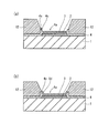
- the end view for demonstrating the process which resulted in 1 aspect of this invention The top view which shows a part of organic electroluminescent display which concerns on embodiment of this invention
- the end view which shows typically the partial cross section of the organic electroluminescent display which concerns on embodiment of this invention Enlarged end view of part B surrounded by the alternate long and short dash line in FIG.
- the inventor of the present invention relates to an organic EL element to which a metal compound is applied, as described in the “Background Art” section, and through extensive research, there is a possibility that the lifetime of the light emitting surface may be reduced due to generation of uneven brightness or local deterioration. I found something new.
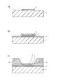
- FIG. 1 is an end view showing a manufacturing process of an organic EL display.
- FIG. 1A shows a state where the first electrode 2, the ITO layer 3, the hole injection layer 4, and the bank 5 are formed on the TFT substrate 1.
- FIG. 1B shows a state in which the light emitting layer 6, the electron injection layer 7, the second electrode 8, and the sealing layer 9 are further formed.
- the recess 4a is formed on the upper surface of the hole injection layer 4 in the process of forming the bank 5 (see FIG. 1A). ).
- the electric field is concentrated near the edge 4c of the recess during light emission.
- a current may flow locally in the light emitting layer 6, and the generation of this local current may cause a problem of shortening the lifetime due to uneven brightness in the light emitting surface or local deterioration. is there.
- the present inventor has suppressed the concentration of charges near the edge of the recess during light emission by covering the edge of the recess formed in the charge injection layer with a part of the bank. As a result, it was possible to conceive the technical feature of suppressing the local current flow in the light emitting layer.
- a stacked body of at least a charge injection layer, a charge transport layer, and a light-emitting layer is interposed between a first electrode and a second electrode, and the shape is defined by a bank.
- the charge injection layer is formed in a recessed structure in which an upper surface sinks in a region defined by the bank, and an edge of the recessed portion in the recessed structure of the charge injection layer is formed on the bank.
- the charge transport layer is partially covered, and the edge of the charge transport layer is formed so as to face the sinked portion of the concave portion of the charge injection layer covered with a part of the bank.
- the edge of the recess formed in the charge injection layer is covered with a part of the bank, it is possible to suppress the electric field from concentrating on the edge of the recess during light emission. It is possible to suppress a current from flowing locally in the layer. Therefore, luminance unevenness in the light emitting surface can be suppressed, and the light emission characteristics can be further improved.
- the charge transport layer may be configured to be in contact with a covering portion that covers the edge of the concave portion of the charge injection layer in the bank.
- the charge transport layer is surrounded by the sinked portion of the concave portion of the charge injection layer in a region defined by the bank and a covering portion covering an edge of the concave portion of the charge injection layer in the bank. It can also be configured to be formed in the region.
- the material constituting the charge injection layer may be a material eroded by a liquid used when forming the bank.
- the liquid may be water or a TMAH solution.
- the material constituting the charge injection layer may be a metal oxide, nitride or oxynitride. These materials are generally hydrophilic. Therefore, the recess can be formed in the cleaning step with pure water during the step of forming the bank.
- a part of the bank may reach the bottom surface of the recess in the recessed structure of the charge injection layer, and the side surface of the bank may be an upward slope from the point of arrival to the bottom surface of the recess.
- a part of the bank may not reach the bottom surface of the concave portion in the concave structure of the charge injection layer.
- the bank material may be fluidized by applying heat treatment to the bank material so that the edge of the recess is covered with a part of the bank material. It is done. According to the above configuration, the bank material does not have to flow to the bottom of the recess, so that the temperature and time of the heat treatment can be reduced to a short time.
- the bank may include an insulating material. Thereby, adjacent light emitting layers can be insulated.
- the light emitting layer may be an organic EL layer.
- the charge injection layer may extend to the side of the bank along the bottom surface of the bank.
- the edge of the concave portion of the charge injection layer may be a convex corner portion formed by a region not recessed in the upper surface of the charge injection transport layer and a side surface of the concave portion.
- a light emitting device which is one embodiment of the present invention includes a plurality of the light emitting elements described above.
- a stacked body of at least a charge injection layer, a charge transport layer, and a light-emitting layer is interposed between the first electrode and the second electrode, and
- a method of manufacturing a light emitting device having a shape defined by a bank the step of forming the charge injection layer, the step of forming a bank material layer made of a material constituting the bank on the charge injection layer, and the bank Removing a part of the material layer to expose a part of the charge injection layer; applying a heat treatment to a remaining portion of the bank material layer on the charge injection layer; Forming a charge transport layer on the charge injection layer; and forming a light emitting layer on the formed charge transport layer, wherein the charge injection layer exposes a part of the charge injection layer.
- the exposed surface of the charge injection layer is formed in a recessed structure that sinks from the level of the bottom surface of the remaining portion of the bank material layer due to the erosion of the liquid.
- the material constituting the bank is extended from the remaining portion to the edge of the recess of the recessed structure, and in the charge transport layer forming step, the edge of the charge transport layer is the bank.
- the charge injection layer covered with a part of the material layer is formed so as to face the exposed surface of the recess.
- an organic EL element using an organic EL material for a light emitting layer will be described as a light emitting element
- an organic EL display will be described as an example of a light emitting device provided with a plurality of light emitting elements.
- the scale of the member in each drawing differs from an actual thing.
- FIG. 2 is a plan view showing a part of the organic EL display according to the embodiment of the present invention.
- the organic EL display 100 is a top emission type organic EL display in which organic EL elements 10a, 10b, and 10c each having an RGB light emitting layer are arranged in a matrix. Each organic EL element functions as a sub-pixel, and a set of three organic EL elements of RGB functions as a pixel.
- a cross-shaped pixel bank 55 is adopted, and the light emitting layers 56 a 1, 56 b 1, 56 c 1 adjacent in the X axis direction are divided by the bank elements 55 a extending in the Y axis direction, and the light emitting layer 56a2, 56b2, and 56c2 are divided.
- the bank elements 55b extending in the X-axis direction divide the light emitting layers 56a1 and 56a2 adjacent in the Y-axis direction, the light emitting layers 56b1 and 56b2, and the light emitting layers 56c1 and 56c2.
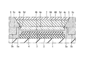
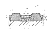
- FIG. 3 is an end view schematically showing a partial cross section of the organic EL display according to the embodiment of the present invention, and shows a cross section taken along line AA of FIG.
- FIG. 4 is an enlarged end view of a portion B surrounded by an alternate long and short dash line in FIG.
- a first electrode 2 as an anode is formed in a matrix on a TFT substrate 1 (hereinafter simply “substrate 1”).
- An ITO (indium tin oxide) layer 3 and a hole are formed on the first electrode 2.
- the injection layer 4 and the hole transport layer 6A are laminated in that order.
- the ITO layer 3 is laminated only on the first electrode 2, whereas the hole injection layer 4 is formed not only on the first electrode 2 but over the entire upper surface of the substrate 1.
- a bank 5 is formed on the upper periphery of the first electrode 2 through a hole injection layer 4, and a hole transport layer 6 A and a light emitting layer 6 B are stacked in a region defined by the bank 5. Further, on the light emitting layer 6B, the electron injection layer 7, the second electrode 8 serving as a cathode, and the sealing layer 9 are adjacent to each other beyond the region defined by the bank 5, and the organic EL elements 10a, 10b, 10c is formed so as to be continuous.
- the substrate 1 is, for example, alkali-free glass, soda glass, non-fluorescent glass, phosphoric acid glass, boric acid glass, quartz, acrylic resin, styrene resin, polycarbonate resin, epoxy resin, polyethylene, polyester, silicone resin. Or an insulating material such as alumina.
- the first electrode 2 is made of Ag (silver).
- the first electrode 2 is, for example, APC (silver, palladium, copper alloy), ARA (silver, rubidium, gold alloy), MoCr (molybdenum and chromium alloy), NiCr (nickel and chromium alloy), etc. It may be formed by. In the case of a top emission type light emitting element, it is preferably formed of a light reflective material.
- the ITO layer 3 is interposed between the first electrode 2 and the hole injection layer 4 and has a function of improving the bonding property between the layers.
- the hole injection layer 4 is formed of WOx (tungsten oxide) or MoxWyOz (molybdenum-tungsten oxide).
- the hole injection layer 4 should just be formed with the metal compound which performs a hole injection function, As such a metal compound, a metal oxide, a metal nitride, or a metal oxynitride is mentioned, for example.
- the hole injection layer 4 When the hole injection layer 4 is formed of a specific metal compound, holes can be easily injected, and electrons can effectively contribute to light emission in the light emitting layer 6B, so that good light emission characteristics can be obtained. it can.
- a specific metal compound a transition metal is preferable. Since the transition metal takes a plurality of oxidation numbers, it can take a plurality of levels. As a result, hole injection becomes easy and the driving voltage can be reduced.
- the hole injection layer 4 extends laterally along the bottom surfaces 5a and 5b of the bank 5, and a part of the top surface is recessed to form a recess 4a.
- a bottom surface 4b as an inner bottom surface portion of the recess 4a is depressed below the level 5c of the bank bottom surface 5a.
- the recess 4a includes a bottom surface 4b and a side surface 4d as an inner side surface continuous with the bottom surface 4b.
- the depth of the recess 4a is approximately 5 nm to 30 nm.
- the edge 4c of the recess is a convex corner portion formed by the region 4e that is not recessed on the upper surface of the hole injection layer 4 and the side surface 4d of the recess, and is covered with the covering portion 5d that is a part of the bank 5. Yes.
- the edge 4c of the recess protrudes with respect to the bottom surface 4b of the recess, if the edge 4c of the recess is not covered with the insulating coating 5d, an electric field concentration occurs here, and the hole transport layer 6A is formed. As a result, a current flows locally to the light emitting layer 6B, and as a result, there arises a problem that the life of the product is shortened due to uneven brightness in the light emitting surface and local deterioration of the light emitting layer 6B.
- the edge 4c of the recess is covered with the insulating covering portion 5d, it is possible to suppress the occurrence of such a problem.
- the thickness of the covering portion 5d (the shortest distance from the edge 4c of the recess to the hole transport layer 6A) be 2 nm to 5 nm.
- the shape of the edge 4c of the recess is made polygonal or rounded rather than the edge shape as shown in FIG. 4 as an example, so that electric field concentration can be further suppressed.
- the covering portion 5d reaches the bottom surface 4b of the recess 4a, and the side surface of the bank 5 is an upward slope from the point reaching the recess bottom surface 4b to the apex.
- the bank 5 is for partitioning the light emitting layer 6B for each sub-pixel, and is formed of an organic material such as resin and has an insulating property.
- organic materials include acrylic resins, polyimide resins, novolac type phenol resins, and the like.
- the bank 5 preferably has organic solvent resistance. Furthermore, since the bank 5 may be subjected to an etching process, a baking process, or the like, it is preferable that the bank 5 be formed of a highly resistant material that does not excessively deform or alter the process.
- the hole transport layer 6A is a layer having a thickness of about 10 nm to 20 nm, and has a function of transporting holes injected from the hole injection layer 4 into the light emitting layer 6B.
- a hole transporting organic material is used as the hole transport layer 6A.
- the hole transporting organic material is an organic substance having a property of transferring generated holes by intermolecular charge transfer reaction. This is sometimes called a p-type organic semiconductor.
- the hole transport layer 6A may be a high molecular material or a low molecular material, but is formed by a wet printing method.
- a cross-linking agent so that it does not easily dissolve into the light-emitting layer 6B.
- a copolymer containing a fluorene moiety and a triarylamine moiety or a low molecular weight triarylamine derivative can be used.
- the crosslinking agent dipentaerythritol hexaacrylate or the like can be used. In this case, it is preferably formed of poly (3,4-ethylenedioxythiophene) doped with polystyrene sulfonic acid (PEDOT-PSS) or a derivative thereof (such as a copolymer).
- the light-emitting layer 6B is an organic light-emitting layer having a thickness of about 50 nm to 80 nm.
- the electron injection layer 7 has a function of transporting electrons injected from the second electrode 8 to the light emitting layer 6B, and is preferably formed of, for example, barium, phthalocyanine, lithium fluoride, or a combination thereof.
- the second electrode 8 is made of, for example, ITO, IZO (indium zinc oxide) or the like. In the case of a top emission type light emitting element, it is preferably formed of a light transmissive material.
- the sealing layer 9 has a function of preventing the light emitting layer 6B and the like from being exposed to moisture or air, and is made of, for example, a material such as SiN (silicon nitride) or SiON (silicon oxynitride). It is formed. In the case of a top emission type light emitting element, it is preferably formed of a light transmissive material.
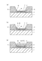
- ⁇ Manufacturing method> 5 to 7 are process diagrams illustrating a method for manufacturing an organic EL display according to an embodiment of the present invention.
- an Ag thin film is formed on a substrate 1 by, for example, sputtering, and the Ag thin film is patterned by, for example, photolithography to form first electrodes 2 in a matrix.
- the Ag thin film may be formed by vacuum deposition or the like.
- an ITO thin film is formed by, for example, sputtering, and the ITO layer 3 is formed by patterning the ITO thin film by, for example, photolithography.
- a thin film 11 of WOx or MoxWyOz is formed by a technique such as vacuum deposition or sputtering using a composition containing WOx or MoxWyOz.
- a bank material layer 12 is formed on the thin film 11 using a bank material made of an organic material, and a part of the bank material layer 12 is removed to remove a part of the thin film 11. To expose.
- the bank material layer 12 can be formed, for example, by coating. The removal of the bank material layer 12 can be performed by patterning using a predetermined developer (tetramethylammonium hydroxide (TMAH) solution or the like).
- TMAH tetramethylammonium hydroxide
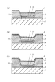
- heat treatment is performed to give a certain degree of fluidity to the remaining portion of the bank material layer 12, and the bank material is extended from the remaining portion to the edge 4c of the recess. As a result, the edge 4c of the recess is covered with the covering portion 5d.
- heat curing can be employed for the heat treatment. The temperature and time of the heat curing may be appropriately determined in consideration of the type of bank material, the required thickness of the covering portion 5d, and the like.
- the surface of the remaining portion of the bank material layer 12 is subjected to a liquid repellent treatment using, for example, fluorine plasma to form the bank 5.
- a hole transport layer 6A is formed in an area defined in the bank 5 based on, for example, a wet printing method.
- a wet printing method The nozzle jet method represented by the inkjet method and the dispenser method can be used.
- the ink jet method the organic film forming material converted into ink is jetted from the nozzle to the metal oxide layer. Thereby, the hole transport layer 6A is formed.
- a composition ink containing an organic EL material (hereinafter simply referred to as an ink jet method) is formed on the hole transport layer 6A formed in the region defined by the bank 5 by, for example, an ink jet method. (Referred to as “ink”) is dropped and the ink is dried to form the light emitting layer 6B.
- the ink may be dropped by a dispenser method, a nozzle coating method, a spin coating method, intaglio printing, letterpress printing, or the like.
- a barium thin film to be the electron injection layer 7 is formed by, for example, vacuum deposition, and as shown in FIG. 7B, an ITO thin film to be the second electrode 8 by, for example, sputtering. As shown in FIG. 7C, a sealing layer 9 is further formed.
- the edge 4c of the recessed portion is covered with the covering portion 5d, and then the hole transport layer 6A and the light emitting layer 6B are formed. Since they are sequentially formed, it is possible to suppress the concentration of the electric field on the edge 4c of the recess.
- the thin film 11 having a uniform thickness is once formed, a part of the surface portion is dissolved at the time of cleaning the etching residue using pure water so as to have a recessed structure.
- the thickness portion in the light emitting region is reduced and the hole injection layer 4 is formed.
- the surface is partially dissolved to form a concave structure, so that the charge injection and transport performance is excellent, and the light emitting region Then, since the thin hole injection layer 4 can be produced efficiently, it is advantageous.
- this invention is not limited to these embodiment.
- the following modifications can be considered.
- WOx or MoxWyOz is used as the material constituting the hole injection layer 4, but generally, metal oxides, nitrides, and oxynitrides are easily eroded by pure water. Even when a metal other than Mo (molybdenum) and W (tungsten) is used, the same effect can be obtained by applying this embodiment.
- the hole injection layer is eroded by pure water during cleaning to form a recess, but if the present invention is adopted, even if the recess is formed for other reasons, An effect of suppressing the concentration of the electric field on the edge of the recess can be obtained.
- Other reasons include, for example, the case where the hole injection layer is eroded by an etching solution during etching or the case where the hole injection layer is eroded by a stripping agent during resist stripping. In this way, when the hole injection layer is made of a material eroded by the liquid used when forming the bank, more specifically, the material eroded by the liquid used with a part of the hole injection layer exposed.
- the present invention is effective when consisting of: (3)
- the covering portion extending from the bank reaches the bottom surface 4b of the concave portion beyond the edge 4c of the concave portion.
- the present invention only needs to cover the edge 4c of the concave portion.
- the covering portion 5 d may not reach the bottom surface 4 b of the recess.
- the bank material does not have to flow to the bottom of the recess, so that the heat treatment temperature and time can be reduced to a short time.
- the present invention uses the max patterning or the like as another forming method. You can also.
- FIG. 6A the lower end of the slope of the bank material 12 and the edge 4c of the recess coincide, but this is not necessarily the case.
- the slope of the bank material 12 may recede to expose a part of the non-recessed region 4e. Even in this case, the bank material 12 may be appropriately heat-treated so that the edge 4c of the recess is covered with a part of the bank material (see FIG. 9B).
- the bank formation step is performed after the hole transport layer is once formed and cleaning after etching is performed, a recess is formed on the surface of the hole transport layer as shown in FIG. It is also assumed that is formed. In this case, a concave portion is formed on the upper surface of the hole transport layer 13, but the edge of the concave portion formed in the hole transport layer is covered with the covering portion. Is prevented.
- the first electrode 2 is formed of an Ag thin film, the ITO layer 3 is formed thereon.
- the ITO layer 3 can be eliminated and the anode can have a single layer structure.
- an organic EL display is described as an example of a light-emitting device including a plurality of light-emitting elements, but the present invention is not limited to this and can be applied to a lighting device or the like.
- a so-called pixel bank is used, but the present invention is not limited to this.
- a line bank (line-shaped bank) can be adopted.
- the line bank 65 is employed, and the light emitting layers 66a, 66b, 66c adjacent in the X-axis direction are divided. As shown in FIG.
- the present invention is not limited to this and may be a bottom emission type.
- the present invention is not limited to this and may be a bottom emission type.
- the electron injection layer is interposed between the light emitting layer and the second electrode.
- an electron transport layer may be interposed.
- an organic material is used as the bank material, but an inorganic material can also be used.
- the bank material layer can be formed by coating, for example, as in the case of using an organic material.
- the removal of the bank material layer can be performed by forming a resist pattern on the bank material layer and then performing etching using a predetermined etching solution (tetramethylammonium hydroxide oxide (TMAH) solution or the like).
- TMAH tetramethylammonium hydroxide oxide
- the resist pattern is removed after etching by, for example, an aqueous or non-aqueous release agent. Next, the etching residue is washed with pure water.
- the material constituting the thin film WOx or MoxWyOz
- the exposed portion of the thin film is eroded to form a concave structure as in the case shown in FIG. It is formed.
- a hole injection layer having a recess is formed.
- the present invention can be applied as in the case where an organic material is used.
- the present invention can be used for an organic EL display or the like.
Abstract
Description
本発明者は、「背景技術」の欄において記載した、金属化合物を適用した有機EL素子に関し、鋭意研究により、発光面内における輝度ムラの発生や局所的な劣化による寿命の低下の可能性があることを新たに見出した。 <Background of obtaining one embodiment of the present invention>
The inventor of the present invention relates to an organic EL element to which a metal compound is applied, as described in the “Background Art” section, and through extensive research, there is a possibility that the lifetime of the light emitting surface may be reduced due to generation of uneven brightness or local deterioration. I found something new.
本発明の一態様である発光素子は、第1電極と第2電極との間に、少なくとも電荷注入層と電荷輸送層と発光層の積層体が介挿され、かつ、バンクで形状が規定された発光素子であって、前記電荷注入層は、前記バンクで規定された領域においては上面が沈下した凹入構造に形成され、前記電荷注入層の凹入構造における凹部の縁は、前記バンクの一部で被覆され、前記電荷輸送層は、その縁が前記バンクの一部で被覆された前記電荷注入層の前記凹部における前記沈下した部分に対向するように形成されている。 <Outline of One Embodiment of Invention>
In a light-emitting element which is one embodiment of the present invention, a stacked body of at least a charge injection layer, a charge transport layer, and a light-emitting layer is interposed between a first electrode and a second electrode, and the shape is defined by a bank. In the light emitting device, the charge injection layer is formed in a recessed structure in which an upper surface sinks in a region defined by the bank, and an edge of the recessed portion in the recessed structure of the charge injection layer is formed on the bank. The charge transport layer is partially covered, and the edge of the charge transport layer is formed so as to face the sinked portion of the concave portion of the charge injection layer covered with a part of the bank.
図2は、本発明の実施形態に係る有機ELディスプレイの一部を示す平面図である。 <Outline configuration>
FIG. 2 is a plan view showing a part of the organic EL display according to the embodiment of the present invention.
基板1は、例えば、無アルカリガラス、ソーダガラス、無蛍光ガラス、燐酸系ガラス、硼酸系ガラス、石英、アクリル系樹脂、スチレン系樹脂、ポリカーボネート系樹脂、エポキシ系樹脂、ポリエチレン、ポリエステル、シリコーン系樹脂、又はアルミナ等の絶縁性材料で形成されている。 <Configuration of each part>
The
図5乃至図7は、本発明の実施形態に係る有機ELディスプレイの製造方法を説明する工程図である。 <Manufacturing method>
5 to 7 are process diagrams illustrating a method for manufacturing an organic EL display according to an embodiment of the present invention.
(1)上記実施形態では、ホール注入層4を構成する材料としてWOx又はMoxWyOzを用いて説明しているが、一般に、金属の酸化物、窒化物、酸窒化物は純水に浸食されやすいので、Mo(モリブデン)、W(タングステン)以外の金属を用いた場合でも本実施形態を適用することにより同様の効果を奏することができる。
(2)上記実施形態では、ホール注入層は洗浄の際に純水に浸食されて凹部が形成されているが、本発明を採用すれば、それ以外の理由により凹部が形成されたとしても、凹部の縁に電界が集中するのを抑制するという効果を得ることができる。それ以外の理由とは、例えば、ホール注入層がエッチングの際にエッチング液に浸食される場合や、レジスト剥離の際に剥離剤に浸食される場合などが挙げられる。このように、ホール注入層がバンクを形成する際に用いられる液体に浸食される材料からなる場合、より詳細には、ホール注入層の一部が露出した状態で用いられる液体に浸食される材料からなる場合に、本発明は有効である。
(3)上記実施形態では、バンクから延出した被覆部は凹部の縁4cを越えて凹部の底面4bまで到達しているが、本発明は、凹部の縁4cを被覆することさえできれば、これに限られない。例えば、図8に示すように、被覆部5dが凹部の底面4bまで到達しない場合でも構わない。図8の構成を採用した場合には、バンク材料を凹部底面まで流さなくてもよいので、熱処理の温度および時間を低温かつ短時間にすることができる。 As mentioned above, although demonstrated based on embodiment, this invention is not limited to these embodiment. For example, the following modifications can be considered.
(1) In the embodiment described above, WOx or MoxWyOz is used as the material constituting the
(2) In the above embodiment, the hole injection layer is eroded by pure water during cleaning to form a recess, but if the present invention is adopted, even if the recess is formed for other reasons, An effect of suppressing the concentration of the electric field on the edge of the recess can be obtained. Other reasons include, for example, the case where the hole injection layer is eroded by an etching solution during etching or the case where the hole injection layer is eroded by a stripping agent during resist stripping. In this way, when the hole injection layer is made of a material eroded by the liquid used when forming the bank, more specifically, the material eroded by the liquid used with a part of the hole injection layer exposed. The present invention is effective when consisting of:
(3) In the above embodiment, the covering portion extending from the bank reaches the
(4)図6(a)では、バンク材料12の斜面の下端と凹部の縁4cとが一致しているが、必ずしもこのようになるとは限らない。バンク材料によっては、図9(a)に示すように、バンク材料12の斜面が後退することにより、凹入されていない領域4eの一部が露出する場合もある。この場合でも、バンク材料12に適切に熱処理を施すことにより、凹部の縁4cをバンク材料の一部で覆わせることとすればよい(図9(b)参照)。
(5)なお、ホール輸送層の材料によっては、ホール輸送層を一旦形成した後にバンク形成工程を実施し、エッチング後の洗浄を行った場合、図10に示すようにホール輸送層の表面に凹部が形成される場合も想定される。この場合、ホール輸送層13の上面に凹部が形成されるが、ホール輸送層に形成された凹部の縁が被覆部で覆われることになるので、やはり駆動時に凹部の縁に電界集中が生じる問題は防止される。
(6)上記実施形態では、第1電極2をAg薄膜で形成しているので、ITO層3をその上に形成することとしている。第1電極2をAl系にしたときは、ITO層3を無くして陽極を単層構造にすることができる。
(7)上記実施形態では、発光素子を複数備えた発光装置として、有機ELディスプレイを例に挙げて説明しているが、本発明はこれに限らず、照明装置等にも適用可能である。
(8)上記実施形態では、所謂、ピクセルバンク(井桁状バンク)を採用しているが、本発明は、これに限らない。例えば、ラインバンク(ライン状のバンク)を採用することができる。図11の例では、ラインバンク65が採用されており、X軸方向に隣接する発光層66a、66b、66cが区分けされる。なお、図11に示すように、ラインバンク65を採用する場合には、Y軸方向に隣接する発光層同士はバンク要素により規定されていないが、駆動方法および陽極のサイズおよび間隔などを適宜設定することにより、互いに影響せず発光させることができる。
(9)上記実施形態では、トップエミッション型で説明しているが、これに限定されず、ボトムエミッション型であっても良い。
(10)上記実施形態では、発光層と第2電極との間に電子注入層のみが介挿されているが、これに加えて電子輸送層が介挿されていることとしてもよい。
(11)上記実施形態では、バンク材料として、有機材料が用いられていたが、無機材料も用いることができる。 In the above embodiment, as an example of the method of forming the
(4) In FIG. 6A, the lower end of the slope of the
(5) Depending on the material of the hole transport layer, when the bank formation step is performed after the hole transport layer is once formed and cleaning after etching is performed, a recess is formed on the surface of the hole transport layer as shown in FIG. It is also assumed that is formed. In this case, a concave portion is formed on the upper surface of the hole transport layer 13, but the edge of the concave portion formed in the hole transport layer is covered with the covering portion. Is prevented.
(6) In the above embodiment, since the
(7) In the above embodiment, an organic EL display is described as an example of a light-emitting device including a plurality of light-emitting elements, but the present invention is not limited to this and can be applied to a lighting device or the like.
(8) In the above embodiment, a so-called pixel bank is used, but the present invention is not limited to this. For example, a line bank (line-shaped bank) can be adopted. In the example of FIG. 11, the
(9) Although the top emission type has been described in the above embodiment, the present invention is not limited to this and may be a bottom emission type.
(10) In the above embodiment, only the electron injection layer is interposed between the light emitting layer and the second electrode. However, in addition to this, an electron transport layer may be interposed.
(11) In the above embodiment, an organic material is used as the bank material, but an inorganic material can also be used.
2 第1電極
3 ITO層
4 ホール注入層
4a 凹部
4b 凹部の底面
4c 凹部の縁
4d 凹部の側面
4e ホール注入層の上面において凹入されていない領域
5 バンク
5a、5b バンクの底面
5c バンクの底面のレベル
5d 被覆部
6A ホール輸送層
6B 発光層
7 電子注入層
8 第2電極
9 封止層
10a、10b、10c 有機EL素子
11 薄膜
12 バンク材料層
13 ホール輸送層
55 ピクセルバンク
55a バンク要素
55b バンク要素
56a1、56a2、56b1、56b2、56c1、56c2 発光層
65 ラインバンク
66a、66b、66c 発光層
100 有機ELディスプレイ DESCRIPTION OF
Claims (14)
- 第1電極と第2電極との間に、少なくとも電荷注入層と電荷輸送層と発光層の積層体が介挿され、かつ、バンクで形状が規定された発光素子であって、
前記電荷注入層は、前記バンクで規定された領域においては上面が沈下した凹入構造に形成され、
前記電荷注入層の凹入構造における凹部の縁は、前記バンクの一部で被覆され、
前記電荷輸送層は、その縁が前記バンクの一部で被覆された前記電荷注入層の前記凹部における前記沈下した部分に対向するように形成されている、
ことを特徴とする発光素子。 A light emitting device in which at least a charge injection layer, a charge transport layer, and a light emitting layer are interposed between the first electrode and the second electrode, and the shape is defined by a bank;
The charge injection layer is formed in a recessed structure with an upper surface sinking in a region defined by the bank,
The edge of the recess in the recess structure of the charge injection layer is covered with a part of the bank,
The charge transport layer is formed so that an edge thereof faces the sinked portion of the concave portion of the charge injection layer covered with a part of the bank.
A light emitting element characterized by the above. - 前記電荷輸送層は、前記バンクにおける、前記電荷注入層の凹部の縁を被覆する被覆部に接触している、
ことを特徴とする請求項1に記載の発光素子。 The charge transport layer is in contact with a covering portion that covers an edge of the concave portion of the charge injection layer in the bank.
The light-emitting element according to claim 1. - 前記電荷輸送層は、前記バンクで規定された領域における前記電荷注入層の前記凹部の前記沈下した部分と、前記バンクにおける前記電荷注入層の凹部の縁を被覆する被覆部とにより囲まれる領域に形成されている、
ことを特徴とする請求項1に記載の発光素子。 The charge transport layer is formed in a region surrounded by the sinked portion of the concave portion of the charge injection layer in the region defined by the bank and a covering portion covering an edge of the concave portion of the charge injection layer in the bank. Formed,
The light-emitting element according to claim 1. - 前記電荷注入層を構成する材料は、前記バンクを形成するときに用いられる液体により浸食される材料である
ことを特徴とする請求項1に記載の発光素子。 The light emitting device according to claim 1, wherein the material constituting the charge injection layer is a material eroded by a liquid used when forming the bank. - 前記液体は水またはTMAH溶液である
ことを特徴とする請求項4に記載の発光素子。 The light emitting device according to claim 4, wherein the liquid is water or a TMAH solution. - 前記電荷注入層を構成する材料は、金属の酸化物、窒化物または酸窒化物である
ことを特徴とする請求項1に記載の発光素子。 The light emitting device according to claim 1, wherein the material constituting the charge injection layer is a metal oxide, nitride, or oxynitride. - 前記バンクの一部は、前記電荷注入層の凹入構造における凹部の底面まで達し、前記バンクの側面は、前記凹部底面への到達点から頂点にかけて上り斜面になっている
ことを特徴とする請求項1に記載の発光素子。 A part of the bank reaches the bottom surface of the recess in the recessed structure of the charge injection layer, and the side surface of the bank is an upward slope from a point reaching the bottom surface of the recess. Item 2. A light emitting device according to Item 1. - 前記バンクの一部は、前記電荷注入層の凹入構造における凹部の底面まで達していない
ことを特徴とする請求項1に記載の発光素子。 2. The light emitting device according to claim 1, wherein a part of the bank does not reach a bottom surface of a concave portion in the concave structure of the charge injection layer. - 前記バンクは、絶縁性を有する材料を含む
ことを特徴とする請求項1記載の発光素子。 The light-emitting element according to claim 1, wherein the bank includes an insulating material. - 前記発光層は、有機EL層であることを特徴とする請求項1に記載の発光素子。 The light emitting device according to claim 1, wherein the light emitting layer is an organic EL layer.
- 前記電荷注入層は、前記バンクの底面に沿って前記バンクの側方に延出している
ことを特徴とする請求項1記載の発光素子。 The light emitting device according to claim 1, wherein the charge injection layer extends to a side of the bank along a bottom surface of the bank. - 前記電荷注入層の前記凹部の縁は、前記電荷注入輸送層の上面において凹入されていない領域と前記凹部の側面とで形成された凸角部分である
ことを特徴とする請求項1に記載の発光素子。 The edge of the concave portion of the charge injection layer is a convex corner portion formed by a region that is not recessed on the upper surface of the charge injection transport layer and a side surface of the concave portion. Light emitting element. - 請求項1~12の何れかに記載の発光素子を複数備えた発光装置。 A light-emitting device comprising a plurality of light-emitting elements according to any one of claims 1 to 12.
- 第1電極と第2電極との間に、少なくとも電荷注入層と電荷輸送層と発光層との積層体が介挿され、かつ、バンクで形状が規定された発光素子の製造方法であって、
前記電荷注入層を形成する工程と、
前記電荷注入層上にバンクを構成する材料からなるバンク材料層を形成する工程と、
前記バンク材料層の一部を除去して前記電荷注入層の一部を露出させる工程と、
前記電荷注入層上の前記バンク材料層の残留部に熱処理を施す工程と、
前記熱処理工程後、前記露出した前記電荷注入層上に電荷輸送層を形成する工程と
前記形成された電荷輸送層上に発光層を形成する工程と、
を含み、
前記電荷注入層は、前記電荷注入層の一部が露出した状態で用いられる液体により浸食される材料からなり、
前記電荷注入層の露出面は、前記液体の浸食により前記バンク材料層の残留部底面のレベルから沈下した凹入構造に形成され、
前記熱処理工程では、前記バンク材料層の残留部に流動性を与えることにより、前記残留部から前記バンクを構成する材料を前記凹入構造の凹部の縁まで延出させ、
前記電荷輸送層形成工程では、前記電荷輸送層は、その縁が前記バンク材料層の一部で被覆された前記電荷注入層の前記凹部における露出面に対向するように形成される、
ことを特徴とする発光素子の製造方法。 A method for manufacturing a light emitting device in which at least a laminate of a charge injection layer, a charge transport layer, and a light emitting layer is interposed between a first electrode and a second electrode, and a shape is defined by a bank,
Forming the charge injection layer;
Forming a bank material layer made of a material constituting the bank on the charge injection layer;
Removing a portion of the bank material layer to expose a portion of the charge injection layer;
Applying a heat treatment to the remaining portion of the bank material layer on the charge injection layer;
After the heat treatment step, a step of forming a charge transport layer on the exposed charge injection layer, a step of forming a light emitting layer on the formed charge transport layer,
Including
The charge injection layer is made of a material eroded by a liquid used in a state where a part of the charge injection layer is exposed,
The exposed surface of the charge injection layer is formed in a recessed structure that sags from the level of the bottom surface of the remaining portion of the bank material layer by erosion of the liquid
In the heat treatment step, by imparting fluidity to the remaining portion of the bank material layer, the material constituting the bank is extended from the remaining portion to the edge of the recessed portion of the recessed structure,
In the charge transport layer forming step, the charge transport layer is formed so that an edge thereof faces an exposed surface of the concave portion of the charge injection layer covered with a part of the bank material layer.
A method for manufacturing a light-emitting element.
Priority Applications (4)
| Application Number | Priority Date | Filing Date | Title |
|---|---|---|---|
| JP2012527469A JP5543600B2 (en) | 2010-08-06 | 2010-08-06 | LIGHT EMITTING ELEMENT, LIGHT EMITTING DEVICE HAVING LIGHT EMITTING ELEMENT, AND LIGHT EMITTING ELEMENT MANUFACTURING METHOD |
| CN201080068373.2A CN103038908B (en) | 2010-08-06 | 2010-08-06 | Light-emitting component, possess the light-emitting device of light-emitting component and the manufacture method of light-emitting component |
| PCT/JP2010/004962 WO2012017491A1 (en) | 2010-08-06 | 2010-08-06 | Light-emitting element, light-emitting device provided with light-emitting element, and light-emitting element production method |
| US13/740,353 US9843010B2 (en) | 2010-08-06 | 2013-01-14 | Light-emitting element, light-emitting device provided with light-emitting element, and light-emitting element production method |
Applications Claiming Priority (1)
| Application Number | Priority Date | Filing Date | Title |
|---|---|---|---|
| PCT/JP2010/004962 WO2012017491A1 (en) | 2010-08-06 | 2010-08-06 | Light-emitting element, light-emitting device provided with light-emitting element, and light-emitting element production method |
Related Child Applications (1)
| Application Number | Title | Priority Date | Filing Date |
|---|---|---|---|
| US13/740,353 Continuation US9843010B2 (en) | 2010-08-06 | 2013-01-14 | Light-emitting element, light-emitting device provided with light-emitting element, and light-emitting element production method |
Publications (1)
| Publication Number | Publication Date |
|---|---|
| WO2012017491A1 true WO2012017491A1 (en) | 2012-02-09 |
Family
ID=45559025
Family Applications (1)
| Application Number | Title | Priority Date | Filing Date |
|---|---|---|---|
| PCT/JP2010/004962 WO2012017491A1 (en) | 2010-08-06 | 2010-08-06 | Light-emitting element, light-emitting device provided with light-emitting element, and light-emitting element production method |
Country Status (4)
| Country | Link |
|---|---|
| US (1) | US9843010B2 (en) |
| JP (1) | JP5543600B2 (en) |
| CN (1) | CN103038908B (en) |
| WO (1) | WO2012017491A1 (en) |
Cited By (4)
| Publication number | Priority date | Publication date | Assignee | Title |
|---|---|---|---|---|
| CN107665916A (en) * | 2016-07-29 | 2018-02-06 | 三星显示有限公司 | Organic light-emitting display device and its manufacture method |
| US10109691B2 (en) | 2014-06-25 | 2018-10-23 | Joled Inc. | Method for manufacturing organic EL display panel |
| US10541367B2 (en) | 2014-04-10 | 2020-01-21 | Joled Inc. | Organic EL display panel production method |
| WO2022259068A1 (en) * | 2021-06-08 | 2022-12-15 | 株式会社半導体エネルギー研究所 | Display device, fabrication method for display device, display module, and electronic equipment |
Families Citing this family (5)
| Publication number | Priority date | Publication date | Assignee | Title |
|---|---|---|---|---|
| US10387911B1 (en) | 2012-06-01 | 2019-08-20 | Integral Ad Science, Inc. | Systems, methods, and media for detecting suspicious activity |
| US10910350B2 (en) * | 2014-05-24 | 2021-02-02 | Hiphoton Co., Ltd. | Structure of a semiconductor array |
| US10304813B2 (en) * | 2015-11-05 | 2019-05-28 | Innolux Corporation | Display device having a plurality of bank structures |
| CN109817826B (en) * | 2019-01-22 | 2020-09-01 | 深圳市华星光电半导体显示技术有限公司 | Manufacturing method of OLED display panel |
| KR20210065239A (en) * | 2019-11-26 | 2021-06-04 | 삼성디스플레이 주식회사 | Display device |
Citations (8)
| Publication number | Priority date | Publication date | Assignee | Title |
|---|---|---|---|---|
| JP2004234901A (en) * | 2003-01-28 | 2004-08-19 | Seiko Epson Corp | Display substrate, organic el display device, manufacturing method of display substrate and electronic apparatus |
| JP2005012173A (en) * | 2003-05-28 | 2005-01-13 | Seiko Epson Corp | Film pattern forming method, device and its manufacturing method, electro-optical device, and electronic apparatus |
| JP2005197189A (en) * | 2004-01-09 | 2005-07-21 | Seiko Epson Corp | Manufacturing method of electrooptical device, and electronic equipment |
| JP2005268099A (en) * | 2004-03-19 | 2005-09-29 | Mitsubishi Electric Corp | Organic el display panel, organic el display device, and method of manufacturing organic el display panel |
| JP2009004347A (en) * | 2007-05-18 | 2009-01-08 | Toppan Printing Co Ltd | Manufacturing method for organic el display element and organic el display element |
| JP2009058897A (en) * | 2007-09-03 | 2009-03-19 | Hitachi Displays Ltd | Display device |
| JP2009218156A (en) * | 2008-03-12 | 2009-09-24 | Casio Comput Co Ltd | El panel and method of manufacturing el panel |
| WO2010032443A1 (en) * | 2008-09-19 | 2010-03-25 | パナソニック株式会社 | Organic electroluminescence element and method for manufacturing same |
Family Cites Families (117)
| Publication number | Priority date | Publication date | Assignee | Title |
|---|---|---|---|---|
| JPH05163488A (en) | 1991-12-17 | 1993-06-29 | Konica Corp | Electroluminescent element of organic thin film |
| US5443922A (en) | 1991-11-07 | 1995-08-22 | Konica Corporation | Organic thin film electroluminescence element |
| US5294869A (en) | 1991-12-30 | 1994-03-15 | Eastman Kodak Company | Organic electroluminescent multicolor image display device |
| US5688551A (en) | 1995-11-13 | 1997-11-18 | Eastman Kodak Company | Method of forming an organic electroluminescent display panel |
| EP1119221B1 (en) | 1996-11-29 | 2004-03-03 | Idemitsu Kosan Company Limited | Organic electroluminescent device |
| JPH10162959A (en) | 1996-11-29 | 1998-06-19 | Idemitsu Kosan Co Ltd | Organic electro-luminescence element |
| JP3782245B2 (en) | 1998-10-28 | 2006-06-07 | Tdk株式会社 | Manufacturing apparatus and manufacturing method of organic EL display device |
| US6309801B1 (en) | 1998-11-18 | 2001-10-30 | U.S. Philips Corporation | Method of manufacturing an electronic device comprising two layers of organic-containing material |
| JP4198253B2 (en) | 1999-02-02 | 2008-12-17 | 出光興産株式会社 | Organic electroluminescence device and method for producing the same |
| US7153592B2 (en) | 2000-08-31 | 2006-12-26 | Fujitsu Limited | Organic EL element and method of manufacturing the same, organic EL display device using the element, organic EL material, and surface emission device and liquid crystal display device using the material |
| JP2002075661A (en) | 2000-08-31 | 2002-03-15 | Fujitsu Ltd | Organic el element and organic el display |
| JP2002318556A (en) | 2001-04-20 | 2002-10-31 | Toshiba Corp | Active matrix type planar display device and manufacturing method therefor |
| TWI257496B (en) | 2001-04-20 | 2006-07-01 | Toshiba Corp | Display device and method of manufacturing the same |
| JP4220253B2 (en) | 2001-05-18 | 2009-02-04 | ケンブリッジ・ユニバーシティ・テクニカル・サービシズ・リミテッド | Electroluminescence device |
| US6697591B2 (en) * | 2001-06-21 | 2004-02-24 | Canon Kabushiki Kaisha | Electrophotographic apparatus and process cartridge |
| JP2003007460A (en) | 2001-06-22 | 2003-01-10 | Sony Corp | Method for manufacturing display equipment, and display equipment |
| JP3823916B2 (en) | 2001-12-18 | 2006-09-20 | セイコーエプソン株式会社 | Display device, electronic apparatus, and display device manufacturing method |
| US6815723B2 (en) * | 2001-12-28 | 2004-11-09 | Semiconductor Energy Laboratory Co., Ltd. | Light emitting device, method of manufacturing the same, and manufacturing apparatus therefor |
| JP2003264083A (en) | 2002-03-08 | 2003-09-19 | Sharp Corp | Organic led element and production process thereof |
| US7086917B2 (en) | 2002-08-12 | 2006-08-08 | National Research Council Of Canada | Photoresist mask/smoothing layer ensuring the field homogeneity and better step-coverage in OLED displays |
| JP4165173B2 (en) | 2002-10-15 | 2008-10-15 | 株式会社デンソー | Manufacturing method of organic EL element |
| JP2004228355A (en) | 2003-01-23 | 2004-08-12 | Seiko Epson Corp | Insulating film substrate, method and apparatus for manufacturing the same, electro-optical device and method for manufacturing the same |
| US7884355B2 (en) | 2003-05-12 | 2011-02-08 | Cambridge Enterprise Ltd | Polymer transistor |
| WO2004100282A2 (en) | 2003-05-12 | 2004-11-18 | Cambridge University Technical Services Limited | Manufacture of a polymer device |
| JP2004363170A (en) | 2003-06-02 | 2004-12-24 | Seiko Epson Corp | Method of forming conductive pattern, electrooptic device, method of manufacturing the same, and electronic equipment |
| US7492090B2 (en) | 2003-09-19 | 2009-02-17 | Semiconductor Energy Laboratory Co., Ltd. | Display device and method for manufacturing the same |
| US7230374B2 (en) | 2003-09-22 | 2007-06-12 | Samsung Sdi Co., Ltd. | Full color organic light-emitting device having color modulation layer |
| US20060139342A1 (en) | 2004-12-29 | 2006-06-29 | Gang Yu | Electronic devices and processes for forming electronic devices |
| JP2005203340A (en) | 2003-12-16 | 2005-07-28 | Matsushita Electric Ind Co Ltd | Organic electroluminescent element |
| ATE433200T1 (en) | 2003-12-16 | 2009-06-15 | Panasonic Corp | ORGANIC ELECTROLUMINENCE COMPONENT AND PRODUCTION METHOD THEREOF |
| JP2005203339A (en) | 2003-12-16 | 2005-07-28 | Matsushita Electric Ind Co Ltd | Organic electroluminescent element and its manufacturing method |
| US20090160325A1 (en) | 2003-12-16 | 2009-06-25 | Panasonic Corporation | Organic electroluminescent device and method for manufacturing the same |
| JP4002949B2 (en) | 2004-03-17 | 2007-11-07 | 独立行政法人科学技術振興機構 | Double-sided organic EL panel |
| JP4645064B2 (en) | 2004-05-19 | 2011-03-09 | セイコーエプソン株式会社 | Manufacturing method of electro-optical device |
| US7541099B2 (en) | 2004-05-21 | 2009-06-02 | Semiconductor Energy Laboratory Co., Ltd. | Anthracene derivative and light emitting element and light emitting device using the same |
| JP4161956B2 (en) | 2004-05-27 | 2008-10-08 | セイコーエプソン株式会社 | Color filter substrate manufacturing method, electro-optical device manufacturing method, electro-optical device, and electronic apparatus |
| CN100490213C (en) | 2004-05-27 | 2009-05-20 | 精工爱普生株式会社 | Method of manufacturing color filter substrate, method of manufacturing electro-optical device, electro-optical device, and electronic apparatus |
| US7211456B2 (en) | 2004-07-09 | 2007-05-01 | Au Optronics Corporation | Method for electro-luminescent display fabrication |
| JP2006185869A (en) | 2004-12-28 | 2006-07-13 | Asahi Glass Co Ltd | Organic electroluminescent element and method of manufacturing the same |
| DE102005007540A1 (en) | 2005-02-18 | 2006-08-31 | Robert Bosch Gmbh | Micromechanical membrane sensor with double membrane |
| JP2006253443A (en) | 2005-03-11 | 2006-09-21 | Seiko Epson Corp | Organic el device, its manufacturing method, and electronic apparatus |
| JP2006294261A (en) | 2005-04-05 | 2006-10-26 | Fuji Electric Holdings Co Ltd | Organic el light-emitting element and its manufacturing method |
| JP2006344459A (en) | 2005-06-08 | 2006-12-21 | Sony Corp | Transfer method and transfer device |
| TWI307612B (en) | 2005-04-27 | 2009-03-11 | Sony Corp | Transfer method and transfer apparatus |
| US7629741B2 (en) | 2005-05-06 | 2009-12-08 | Eastman Kodak Company | OLED electron-injecting layer |
| US7994711B2 (en) | 2005-08-08 | 2011-08-09 | Semiconductor Energy Laboratory Co., Ltd. | Light emitting device and manufacturing method thereof |
| JP2007073499A (en) | 2005-08-08 | 2007-03-22 | Semiconductor Energy Lab Co Ltd | Light-emitting device and its manufacturing method |
| GB0517195D0 (en) | 2005-08-23 | 2005-09-28 | Cambridge Display Tech Ltd | Molecular electronic device structures and fabrication methods |
| KR100958480B1 (en) | 2005-09-29 | 2010-05-17 | 파나소닉 주식회사 | Organic el display and method for manufacturing same |
| JP2007095606A (en) | 2005-09-30 | 2007-04-12 | Seiko Epson Corp | Organic el device, its manufacturing method, and electronics device |
| JP2007150258A (en) | 2005-10-27 | 2007-06-14 | Seiko Epson Corp | Pattern forming method, film structure, electro-optic device, and electronic apparatus |
| JP4318689B2 (en) | 2005-12-09 | 2009-08-26 | 出光興産株式会社 | N-type inorganic semiconductor, n-type inorganic semiconductor thin film, and manufacturing method thereof |
| JP5256605B2 (en) * | 2006-01-18 | 2013-08-07 | 凸版印刷株式会社 | Method for manufacturing organic electroluminescence element |
| JP2007214066A (en) | 2006-02-13 | 2007-08-23 | Seiko Epson Corp | Manufacturing method of organic electroluminescent device |
| US20070241665A1 (en) | 2006-04-12 | 2007-10-18 | Matsushita Electric Industrial Co., Ltd. | Organic electroluminescent element, and manufacturing method thereof, as well as display device and exposure apparatus using the same |
| JP2007288074A (en) | 2006-04-19 | 2007-11-01 | Matsushita Electric Ind Co Ltd | Organic electroluminescence element and manufacturing method thereof |
| JP2007287353A (en) | 2006-04-12 | 2007-11-01 | Matsushita Electric Ind Co Ltd | Manufacturing method of organic electroluminescent element and organic electroluminescent element formed using it |
| JP2007288071A (en) | 2006-04-19 | 2007-11-01 | Matsushita Electric Ind Co Ltd | Organic electroluminescent element, method of manufacturing the same, and display device and exposure device using the same |
| US20070290604A1 (en) | 2006-06-16 | 2007-12-20 | Matsushita Electric Industrial Co., Ltd. | Organic electroluminescent device and method of producing the same |
| JP2008041747A (en) | 2006-08-02 | 2008-02-21 | Matsushita Electric Ind Co Ltd | Organic electroluminescent light-emitting apparatus and manufacturing method thereof |
| JP4915650B2 (en) | 2006-08-25 | 2012-04-11 | パナソニック株式会社 | Organic electroluminescence device |
| JP2008091072A (en) | 2006-09-29 | 2008-04-17 | Seiko Epson Corp | Electro-optical device and its manufacturing method |
| JP2008108530A (en) | 2006-10-25 | 2008-05-08 | Hitachi Displays Ltd | Organic el display device |
| JP4915913B2 (en) | 2006-11-13 | 2012-04-11 | パナソニック株式会社 | Organic electroluminescence device |
| JP2008140724A (en) | 2006-12-05 | 2008-06-19 | Toppan Printing Co Ltd | Organic el element and manufacturing method of same |
| WO2008075615A1 (en) | 2006-12-21 | 2008-06-26 | Semiconductor Energy Laboratory Co., Ltd. | Light-emitting element and light-emitting device |
| JP4998710B2 (en) | 2007-03-06 | 2012-08-15 | カシオ計算機株式会社 | Manufacturing method of display device |
| JP5326289B2 (en) | 2007-03-23 | 2013-10-30 | 凸版印刷株式会社 | ORGANIC EL ELEMENT AND DISPLAY DEVICE INCLUDING THE SAME |
| WO2008120714A1 (en) | 2007-03-29 | 2008-10-09 | Dai Nippon Printing Co., Ltd. | Organic electroluminescent element and process for producing the same |
| EP2151867B1 (en) | 2007-05-30 | 2016-08-03 | Joled Inc. | Organic el display panel |
| EP2077698B1 (en) | 2007-05-31 | 2011-09-07 | Panasonic Corporation | Organic el device and method for manufacturing the same |
| JP5384856B2 (en) | 2007-06-04 | 2014-01-08 | 株式会社半導体エネルギー研究所 | Organometallic complex, light-emitting element, light-emitting device, lighting device, and electronic device |
| KR101581475B1 (en) | 2007-07-31 | 2015-12-30 | 스미또모 가가꾸 가부시키가이샤 | Organic electroluminescence element and method for manufacturing the same |
| JP5001745B2 (en) | 2007-08-10 | 2012-08-15 | 住友化学株式会社 | Organic electroluminescence device and manufacturing method |
| JP2009048960A (en) | 2007-08-23 | 2009-03-05 | Canon Inc | Electrode cleaning treatment method |
| US20090096716A1 (en) * | 2007-09-12 | 2009-04-16 | Lg Electronics Inc. | Display device |
| US8083956B2 (en) | 2007-10-11 | 2011-12-27 | Semiconductor Energy Laboratory Co., Ltd. | Display device and method for manufacturing display device |
| JP2009135053A (en) | 2007-11-30 | 2009-06-18 | Sumitomo Chemical Co Ltd | Electronic device, display device, and method of manufacturing electronic device |
| WO2009075075A1 (en) | 2007-12-10 | 2009-06-18 | Panasonic Corporation | Organic el device, el display panel, method for manufacturing the organic el device and method for manufacturing the el display panel |
| JP4439589B2 (en) | 2007-12-28 | 2010-03-24 | パナソニック株式会社 | Organic EL device, organic EL display panel, and manufacturing method thereof |
| EP2270896B1 (en) | 2008-02-28 | 2014-12-24 | Panasonic Corporation | Organic el display panel |
| JP5267246B2 (en) | 2008-03-26 | 2013-08-21 | 凸版印刷株式会社 | ORGANIC ELECTROLUMINESCENT ELEMENT, ITS MANUFACTURING METHOD, AND ORGANIC ELECTROLUMINESCENT DISPLAY |
| JP2009239180A (en) | 2008-03-28 | 2009-10-15 | Sumitomo Chemical Co Ltd | Organic electroluminescent device |
| KR100999739B1 (en) | 2008-04-02 | 2010-12-08 | 엘지이노텍 주식회사 | Light emitting device and method for fabricating the same |
| US8860009B2 (en) | 2008-04-28 | 2014-10-14 | Dai Nippon Printing Co., Ltd. | Device comprising positive hole injection transport layer, method for producing the same and ink for forming positive hole injection transport layer |
| JP4931858B2 (en) | 2008-05-13 | 2012-05-16 | パナソニック株式会社 | Method for manufacturing organic electroluminescent device |
| JP4678421B2 (en) | 2008-05-16 | 2011-04-27 | ソニー株式会社 | Display device |
| JP4975064B2 (en) | 2008-05-28 | 2012-07-11 | パナソニック株式会社 | Light emitting device and manufacturing method thereof |
| JP2008241238A (en) | 2008-05-28 | 2008-10-09 | Mitsubishi Electric Corp | Refrigerating air conditioner and control method for refrigerating air conditioner |
| CN101689559B (en) | 2008-06-06 | 2011-12-28 | 松下电器产业株式会社 | Organic el display panel and manufacturing method thereof |
| JP2010021138A (en) | 2008-06-09 | 2010-01-28 | Panasonic Corp | Organic electroluminescent device and its manufacturing method |
| GB0811199D0 (en) | 2008-06-18 | 2008-07-23 | Cambridge Entpr Ltd | Electro-optic diode devices |
| US20090315027A1 (en) | 2008-06-24 | 2009-12-24 | Casio Computer Co., Ltd. | Light emitting device and manufacturing method of light emitting device |
| JP4697265B2 (en) | 2008-06-24 | 2011-06-08 | カシオ計算機株式会社 | Method for manufacturing light emitting device |
| JP5199773B2 (en) | 2008-07-30 | 2013-05-15 | 住友化学株式会社 | Organic electroluminescence device and method for producing the same |
| JP5138542B2 (en) | 2008-10-24 | 2013-02-06 | パナソニック株式会社 | Organic electroluminescence device and method for manufacturing the same |
| JP2011040167A (en) | 2008-11-12 | 2011-02-24 | Panasonic Corp | Display and its manufacturing method |
| JP2010123716A (en) | 2008-11-19 | 2010-06-03 | Fujifilm Corp | Organic electroluminescent element |
| JP4856753B2 (en) | 2008-12-10 | 2012-01-18 | パナソニック株式会社 | OPTICAL ELEMENT AND METHOD FOR MANUFACTURING DISPLAY DEVICE HAVING OPTICAL ELEMENT |
| WO2010070798A1 (en) | 2008-12-18 | 2010-06-24 | パナソニック株式会社 | Organic electroluminescent display device and method for manufacturing same |
| JP2010153127A (en) | 2008-12-24 | 2010-07-08 | Sony Corp | Display device |
| JP2010161185A (en) | 2009-01-08 | 2010-07-22 | Ulvac Japan Ltd | Organic el display device and method of manufacturing the same |
| EP2398083B1 (en) | 2009-02-10 | 2018-06-13 | Joled Inc. | Light-emitting element, display device, and method for manufacturing light-emitting element |
| KR20110126594A (en) | 2009-02-10 | 2011-11-23 | 파나소닉 주식회사 | Light-emitting element, light-emitting device comprising light-emitting element, and method for manufacturing light-emitting element |
| WO2011013523A1 (en) | 2009-07-31 | 2011-02-03 | Semiconductor Energy Laboratory Co., Ltd. | Semiconductor device and method for manufacturing the same |
| JP5437736B2 (en) | 2009-08-19 | 2014-03-12 | パナソニック株式会社 | Organic EL device |
| EP2475226B1 (en) | 2009-08-31 | 2017-08-02 | Joled Inc. | Light emitting element and method for producing the same, and light emitting device |
| WO2011077477A1 (en) | 2009-12-22 | 2011-06-30 | パナソニック株式会社 | Display device and method for manufacturing same |
| JP5574114B2 (en) | 2009-12-22 | 2014-08-20 | パナソニック株式会社 | Display device and manufacturing method thereof |
| JP5574112B2 (en) | 2009-12-22 | 2014-08-20 | パナソニック株式会社 | Display device and manufacturing method thereof |
| CN102334384B (en) | 2010-02-22 | 2015-01-28 | 松下电器产业株式会社 | Light-emitting device and method for producing same |
| WO2012017502A1 (en) | 2010-08-06 | 2012-02-09 | パナソニック株式会社 | Organic electroluminescence element and method of manufacturing thereof |
| CN103053041B (en) | 2010-08-06 | 2015-11-25 | 株式会社日本有机雷特显示器 | Organic el element |
| CN103053040B (en) | 2010-08-06 | 2015-09-02 | 株式会社日本有机雷特显示器 | Organic el element |
| JP5612691B2 (en) | 2010-08-06 | 2014-10-22 | パナソニック株式会社 | Organic EL device and method for manufacturing the same |
| JP5677433B2 (en) | 2010-08-06 | 2015-02-25 | パナソニック株式会社 | ORGANIC EL ELEMENT, DISPLAY DEVICE AND LIGHT EMITTING DEVICE |
| JP5677436B2 (en) | 2010-08-06 | 2015-02-25 | パナソニック株式会社 | Organic EL device |
-
2010
- 2010-08-06 WO PCT/JP2010/004962 patent/WO2012017491A1/en active Application Filing
- 2010-08-06 JP JP2012527469A patent/JP5543600B2/en active Active
- 2010-08-06 CN CN201080068373.2A patent/CN103038908B/en active Active
-
2013
- 2013-01-14 US US13/740,353 patent/US9843010B2/en active Active
Patent Citations (8)
| Publication number | Priority date | Publication date | Assignee | Title |
|---|---|---|---|---|
| JP2004234901A (en) * | 2003-01-28 | 2004-08-19 | Seiko Epson Corp | Display substrate, organic el display device, manufacturing method of display substrate and electronic apparatus |
| JP2005012173A (en) * | 2003-05-28 | 2005-01-13 | Seiko Epson Corp | Film pattern forming method, device and its manufacturing method, electro-optical device, and electronic apparatus |
| JP2005197189A (en) * | 2004-01-09 | 2005-07-21 | Seiko Epson Corp | Manufacturing method of electrooptical device, and electronic equipment |
| JP2005268099A (en) * | 2004-03-19 | 2005-09-29 | Mitsubishi Electric Corp | Organic el display panel, organic el display device, and method of manufacturing organic el display panel |
| JP2009004347A (en) * | 2007-05-18 | 2009-01-08 | Toppan Printing Co Ltd | Manufacturing method for organic el display element and organic el display element |
| JP2009058897A (en) * | 2007-09-03 | 2009-03-19 | Hitachi Displays Ltd | Display device |
| JP2009218156A (en) * | 2008-03-12 | 2009-09-24 | Casio Comput Co Ltd | El panel and method of manufacturing el panel |
| WO2010032443A1 (en) * | 2008-09-19 | 2010-03-25 | パナソニック株式会社 | Organic electroluminescence element and method for manufacturing same |
Cited By (5)
| Publication number | Priority date | Publication date | Assignee | Title |
|---|---|---|---|---|
| US10541367B2 (en) | 2014-04-10 | 2020-01-21 | Joled Inc. | Organic EL display panel production method |
| US10109691B2 (en) | 2014-06-25 | 2018-10-23 | Joled Inc. | Method for manufacturing organic EL display panel |
| CN107665916A (en) * | 2016-07-29 | 2018-02-06 | 三星显示有限公司 | Organic light-emitting display device and its manufacture method |
| CN107665916B (en) * | 2016-07-29 | 2023-08-11 | 三星显示有限公司 | Organic light emitting display device and method of manufacturing the same |
| WO2022259068A1 (en) * | 2021-06-08 | 2022-12-15 | 株式会社半導体エネルギー研究所 | Display device, fabrication method for display device, display module, and electronic equipment |
Also Published As
| Publication number | Publication date |
|---|---|
| CN103038908A (en) | 2013-04-10 |
| CN103038908B (en) | 2016-01-06 |
| JPWO2012017491A1 (en) | 2013-09-19 |
| US9843010B2 (en) | 2017-12-12 |
| US20130126844A1 (en) | 2013-05-23 |
| JP5543600B2 (en) | 2014-07-09 |
Similar Documents
| Publication | Publication Date | Title |
|---|---|---|
| JP5357194B2 (en) | LIGHT EMITTING ELEMENT, LIGHT EMITTING DEVICE HAVING LIGHT EMITTING ELEMENT, AND METHOD FOR MANUFACTURING LIGHT EMITTING ELEMENT | |
| JP5543600B2 (en) | LIGHT EMITTING ELEMENT, LIGHT EMITTING DEVICE HAVING LIGHT EMITTING ELEMENT, AND LIGHT EMITTING ELEMENT MANUFACTURING METHOD | |
| JP5426527B2 (en) | LIGHT EMITTING ELEMENT, MANUFACTURING METHOD THEREOF, AND LIGHT EMITTING DEVICE | |
| JP5658256B2 (en) | LIGHT EMITTING ELEMENT, MANUFACTURING METHOD THEREOF, AND LIGHT EMITTING DEVICE | |
| US20100171415A1 (en) | Light-emitting device and display apparatus | |
| US8927975B2 (en) | Light emitting element, method for manufacturing same, and light emitting device | |
| US20150155516A1 (en) | Organic light-emitting element and production method therefor | |
| JP6019376B2 (en) | Organic EL display panel | |
| US20150028315A1 (en) | Organic light-emitting device and method for producing same | |
| JP5620495B2 (en) | LIGHT EMITTING ELEMENT, LIGHT EMITTING DEVICE HAVING LIGHT EMITTING ELEMENT, AND LIGHT EMITTING ELEMENT MANUFACTURING METHOD | |
| JP5543599B2 (en) | Method for manufacturing light emitting device | |
| JP6040445B2 (en) | Organic EL panel and manufacturing method thereof | |
| JP2011187276A (en) | Method of manufacturing conductive film pattern, and method of manufacturing organic el display panel |
Legal Events
| Date | Code | Title | Description |
|---|---|---|---|
| WWE | Wipo information: entry into national phase |
Ref document number: 201080068373.2 Country of ref document: CN |
|
| 121 | Ep: the epo has been informed by wipo that ep was designated in this application |
Ref document number: 10855583 Country of ref document: EP Kind code of ref document: A1 |
|
| WWE | Wipo information: entry into national phase |
Ref document number: 2012527469 Country of ref document: JP |
|
| NENP | Non-entry into the national phase |
Ref country code: DE |
|
| 122 | Ep: pct application non-entry in european phase |
Ref document number: 10855583 Country of ref document: EP Kind code of ref document: A1 |