WO2012015052A1 - 積層構造体、それを用いた電子デバイス、芳香族化合物及び該化合物の製造方法 - Google Patents
積層構造体、それを用いた電子デバイス、芳香族化合物及び該化合物の製造方法 Download PDFInfo
- Publication number
- WO2012015052A1 WO2012015052A1 PCT/JP2011/067550 JP2011067550W WO2012015052A1 WO 2012015052 A1 WO2012015052 A1 WO 2012015052A1 JP 2011067550 W JP2011067550 W JP 2011067550W WO 2012015052 A1 WO2012015052 A1 WO 2012015052A1
- Authority
- WO
- WIPO (PCT)
- Prior art keywords
- group
- formula
- aromatic compound
- represented
- layer
- Prior art date
- Legal status (The legal status is an assumption and is not a legal conclusion. Google has not performed a legal analysis and makes no representation as to the accuracy of the status listed.)
- Ceased
Links
Classifications
-
- C—CHEMISTRY; METALLURGY
- C07—ORGANIC CHEMISTRY
- C07C—ACYCLIC OR CARBOCYCLIC COMPOUNDS
- C07C211/00—Compounds containing amino groups bound to a carbon skeleton
- C07C211/43—Compounds containing amino groups bound to a carbon skeleton having amino groups bound to carbon atoms of six-membered aromatic rings of the carbon skeleton
- C07C211/54—Compounds containing amino groups bound to a carbon skeleton having amino groups bound to carbon atoms of six-membered aromatic rings of the carbon skeleton having amino groups bound to two or three six-membered aromatic rings
- C07C211/56—Compounds containing amino groups bound to a carbon skeleton having amino groups bound to carbon atoms of six-membered aromatic rings of the carbon skeleton having amino groups bound to two or three six-membered aromatic rings the carbon skeleton being further substituted by halogen atoms or by nitro or nitroso groups
-
- C—CHEMISTRY; METALLURGY
- C07—ORGANIC CHEMISTRY
- C07C—ACYCLIC OR CARBOCYCLIC COMPOUNDS
- C07C211/00—Compounds containing amino groups bound to a carbon skeleton
- C07C211/62—Quaternary ammonium compounds
- C07C211/63—Quaternary ammonium compounds having quaternised nitrogen atoms bound to acyclic carbon atoms
-
- C—CHEMISTRY; METALLURGY
- C07—ORGANIC CHEMISTRY
- C07D—HETEROCYCLIC COMPOUNDS
- C07D209/00—Heterocyclic compounds containing five-membered rings, condensed with other rings, with one nitrogen atom as the only ring hetero atom
- C07D209/56—Ring systems containing three or more rings
- C07D209/80—[b, c]- or [b, d]-condensed
- C07D209/82—Carbazoles; Hydrogenated carbazoles
- C07D209/86—Carbazoles; Hydrogenated carbazoles with only hydrogen atoms, hydrocarbon or substituted hydrocarbon radicals, directly attached to carbon atoms of the ring system
-
- C—CHEMISTRY; METALLURGY
- C07—ORGANIC CHEMISTRY
- C07F—ACYCLIC, CARBOCYCLIC OR HETEROCYCLIC COMPOUNDS CONTAINING ELEMENTS OTHER THAN CARBON, HYDROGEN, HALOGEN, OXYGEN, NITROGEN, SULFUR, SELENIUM OR TELLURIUM
- C07F5/00—Compounds containing elements of Groups 3 or 13 of the Periodic Table
- C07F5/02—Boron compounds
- C07F5/025—Boronic and borinic acid compounds
-
- C—CHEMISTRY; METALLURGY
- C07—ORGANIC CHEMISTRY
- C07F—ACYCLIC, CARBOCYCLIC OR HETEROCYCLIC COMPOUNDS CONTAINING ELEMENTS OTHER THAN CARBON, HYDROGEN, HALOGEN, OXYGEN, NITROGEN, SULFUR, SELENIUM OR TELLURIUM
- C07F9/00—Compounds containing elements of Groups 5 or 15 of the Periodic Table
- C07F9/02—Phosphorus compounds
- C07F9/28—Phosphorus compounds with one or more P—C bonds
- C07F9/54—Quaternary phosphonium compounds
- C07F9/5407—Acyclic saturated phosphonium compounds
-
- C—CHEMISTRY; METALLURGY
- C07—ORGANIC CHEMISTRY
- C07F—ACYCLIC, CARBOCYCLIC OR HETEROCYCLIC COMPOUNDS CONTAINING ELEMENTS OTHER THAN CARBON, HYDROGEN, HALOGEN, OXYGEN, NITROGEN, SULFUR, SELENIUM OR TELLURIUM
- C07F9/00—Compounds containing elements of Groups 5 or 15 of the Periodic Table
- C07F9/02—Phosphorus compounds
- C07F9/28—Phosphorus compounds with one or more P—C bonds
- C07F9/54—Quaternary phosphonium compounds
- C07F9/5442—Aromatic phosphonium compounds (P-C aromatic linkage)
-
- C—CHEMISTRY; METALLURGY
- C07—ORGANIC CHEMISTRY
- C07F—ACYCLIC, CARBOCYCLIC OR HETEROCYCLIC COMPOUNDS CONTAINING ELEMENTS OTHER THAN CARBON, HYDROGEN, HALOGEN, OXYGEN, NITROGEN, SULFUR, SELENIUM OR TELLURIUM
- C07F9/00—Compounds containing elements of Groups 5 or 15 of the Periodic Table
- C07F9/02—Phosphorus compounds
- C07F9/28—Phosphorus compounds with one or more P—C bonds
- C07F9/54—Quaternary phosphonium compounds
- C07F9/5456—Arylalkanephosphonium compounds
-
- C—CHEMISTRY; METALLURGY
- C07—ORGANIC CHEMISTRY
- C07F—ACYCLIC, CARBOCYCLIC OR HETEROCYCLIC COMPOUNDS CONTAINING ELEMENTS OTHER THAN CARBON, HYDROGEN, HALOGEN, OXYGEN, NITROGEN, SULFUR, SELENIUM OR TELLURIUM
- C07F9/00—Compounds containing elements of Groups 5 or 15 of the Periodic Table
- C07F9/02—Phosphorus compounds
- C07F9/547—Heterocyclic compounds, e.g. containing phosphorus as a ring hetero atom
- C07F9/553—Heterocyclic compounds, e.g. containing phosphorus as a ring hetero atom having one nitrogen atom as the only ring hetero atom
- C07F9/572—Five-membered rings
- C07F9/5728—Five-membered rings condensed with carbocyclic rings or carbocyclic ring systems
-
- C—CHEMISTRY; METALLURGY
- C08—ORGANIC MACROMOLECULAR COMPOUNDS; THEIR PREPARATION OR CHEMICAL WORKING-UP; COMPOSITIONS BASED THEREON
- C08G—MACROMOLECULAR COMPOUNDS OBTAINED OTHERWISE THAN BY REACTIONS ONLY INVOLVING UNSATURATED CARBON-TO-CARBON BONDS
- C08G61/00—Macromolecular compounds obtained by reactions forming a carbon-to-carbon link in the main chain of the macromolecule
- C08G61/12—Macromolecular compounds containing atoms other than carbon in the main chain of the macromolecule
-
- H—ELECTRICITY
- H10—SEMICONDUCTOR DEVICES; ELECTRIC SOLID-STATE DEVICES NOT OTHERWISE PROVIDED FOR
- H10K—ORGANIC ELECTRIC SOLID-STATE DEVICES
- H10K50/00—Organic light-emitting devices
- H10K50/10—OLEDs or polymer light-emitting diodes [PLED]
- H10K50/14—Carrier transporting layers
- H10K50/15—Hole transporting layers
-
- H—ELECTRICITY
- H10—SEMICONDUCTOR DEVICES; ELECTRIC SOLID-STATE DEVICES NOT OTHERWISE PROVIDED FOR
- H10K—ORGANIC ELECTRIC SOLID-STATE DEVICES
- H10K85/00—Organic materials used in the body or electrodes of devices covered by this subclass
- H10K85/10—Organic polymers or oligomers
- H10K85/111—Organic polymers or oligomers comprising aromatic, heteroaromatic, or aryl chains, e.g. polyaniline, polyphenylene or polyphenylene vinylene
-
- C—CHEMISTRY; METALLURGY
- C08—ORGANIC MACROMOLECULAR COMPOUNDS; THEIR PREPARATION OR CHEMICAL WORKING-UP; COMPOSITIONS BASED THEREON
- C08G—MACROMOLECULAR COMPOUNDS OBTAINED OTHERWISE THAN BY REACTIONS ONLY INVOLVING UNSATURATED CARBON-TO-CARBON BONDS
- C08G2261/00—Macromolecular compounds obtained by reactions forming a carbon-to-carbon link in the main chain of the macromolecule
- C08G2261/10—Definition of the polymer structure
- C08G2261/14—Side-groups
- C08G2261/142—Side-chains containing oxygen
- C08G2261/1424—Side-chains containing oxygen containing ether groups, including alkoxy
-
- C—CHEMISTRY; METALLURGY
- C08—ORGANIC MACROMOLECULAR COMPOUNDS; THEIR PREPARATION OR CHEMICAL WORKING-UP; COMPOSITIONS BASED THEREON
- C08G—MACROMOLECULAR COMPOUNDS OBTAINED OTHERWISE THAN BY REACTIONS ONLY INVOLVING UNSATURATED CARBON-TO-CARBON BONDS
- C08G2261/00—Macromolecular compounds obtained by reactions forming a carbon-to-carbon link in the main chain of the macromolecule
- C08G2261/30—Monomer units or repeat units incorporating structural elements in the main chain
- C08G2261/31—Monomer units or repeat units incorporating structural elements in the main chain incorporating aromatic structural elements in the main chain
- C08G2261/312—Non-condensed aromatic systems, e.g. benzene
-
- C—CHEMISTRY; METALLURGY
- C08—ORGANIC MACROMOLECULAR COMPOUNDS; THEIR PREPARATION OR CHEMICAL WORKING-UP; COMPOSITIONS BASED THEREON
- C08G—MACROMOLECULAR COMPOUNDS OBTAINED OTHERWISE THAN BY REACTIONS ONLY INVOLVING UNSATURATED CARBON-TO-CARBON BONDS
- C08G2261/00—Macromolecular compounds obtained by reactions forming a carbon-to-carbon link in the main chain of the macromolecule
- C08G2261/30—Monomer units or repeat units incorporating structural elements in the main chain
- C08G2261/31—Monomer units or repeat units incorporating structural elements in the main chain incorporating aromatic structural elements in the main chain
- C08G2261/316—Monomer units or repeat units incorporating structural elements in the main chain incorporating aromatic structural elements in the main chain bridged by heteroatoms, e.g. N, P, Si or B
- C08G2261/3162—Arylamines
-
- C—CHEMISTRY; METALLURGY
- C08—ORGANIC MACROMOLECULAR COMPOUNDS; THEIR PREPARATION OR CHEMICAL WORKING-UP; COMPOSITIONS BASED THEREON
- C08G—MACROMOLECULAR COMPOUNDS OBTAINED OTHERWISE THAN BY REACTIONS ONLY INVOLVING UNSATURATED CARBON-TO-CARBON BONDS
- C08G2261/00—Macromolecular compounds obtained by reactions forming a carbon-to-carbon link in the main chain of the macromolecule
- C08G2261/40—Polymerisation processes
- C08G2261/41—Organometallic coupling reactions
- C08G2261/411—Suzuki reactions
-
- C—CHEMISTRY; METALLURGY
- C08—ORGANIC MACROMOLECULAR COMPOUNDS; THEIR PREPARATION OR CHEMICAL WORKING-UP; COMPOSITIONS BASED THEREON
- C08G—MACROMOLECULAR COMPOUNDS OBTAINED OTHERWISE THAN BY REACTIONS ONLY INVOLVING UNSATURATED CARBON-TO-CARBON BONDS
- C08G2261/00—Macromolecular compounds obtained by reactions forming a carbon-to-carbon link in the main chain of the macromolecule
- C08G2261/50—Physical properties
- C08G2261/51—Charge transport
- C08G2261/512—Hole transport
-
- C—CHEMISTRY; METALLURGY
- C08—ORGANIC MACROMOLECULAR COMPOUNDS; THEIR PREPARATION OR CHEMICAL WORKING-UP; COMPOSITIONS BASED THEREON
- C08G—MACROMOLECULAR COMPOUNDS OBTAINED OTHERWISE THAN BY REACTIONS ONLY INVOLVING UNSATURATED CARBON-TO-CARBON BONDS
- C08G2261/00—Macromolecular compounds obtained by reactions forming a carbon-to-carbon link in the main chain of the macromolecule
- C08G2261/90—Applications
- C08G2261/91—Photovoltaic applications
-
- C—CHEMISTRY; METALLURGY
- C08—ORGANIC MACROMOLECULAR COMPOUNDS; THEIR PREPARATION OR CHEMICAL WORKING-UP; COMPOSITIONS BASED THEREON
- C08G—MACROMOLECULAR COMPOUNDS OBTAINED OTHERWISE THAN BY REACTIONS ONLY INVOLVING UNSATURATED CARBON-TO-CARBON BONDS
- C08G2261/00—Macromolecular compounds obtained by reactions forming a carbon-to-carbon link in the main chain of the macromolecule
- C08G2261/90—Applications
- C08G2261/92—TFT applications
-
- C—CHEMISTRY; METALLURGY
- C08—ORGANIC MACROMOLECULAR COMPOUNDS; THEIR PREPARATION OR CHEMICAL WORKING-UP; COMPOSITIONS BASED THEREON
- C08G—MACROMOLECULAR COMPOUNDS OBTAINED OTHERWISE THAN BY REACTIONS ONLY INVOLVING UNSATURATED CARBON-TO-CARBON BONDS
- C08G2261/00—Macromolecular compounds obtained by reactions forming a carbon-to-carbon link in the main chain of the macromolecule
- C08G2261/90—Applications
- C08G2261/95—Use in organic luminescent diodes
-
- Y—GENERAL TAGGING OF NEW TECHNOLOGICAL DEVELOPMENTS; GENERAL TAGGING OF CROSS-SECTIONAL TECHNOLOGIES SPANNING OVER SEVERAL SECTIONS OF THE IPC; TECHNICAL SUBJECTS COVERED BY FORMER USPC CROSS-REFERENCE ART COLLECTIONS [XRACs] AND DIGESTS
- Y02—TECHNOLOGIES OR APPLICATIONS FOR MITIGATION OR ADAPTATION AGAINST CLIMATE CHANGE
- Y02E—REDUCTION OF GREENHOUSE GAS [GHG] EMISSIONS, RELATED TO ENERGY GENERATION, TRANSMISSION OR DISTRIBUTION
- Y02E10/00—Energy generation through renewable energy sources
- Y02E10/50—Photovoltaic [PV] energy
- Y02E10/549—Organic PV cells
-
- Y—GENERAL TAGGING OF NEW TECHNOLOGICAL DEVELOPMENTS; GENERAL TAGGING OF CROSS-SECTIONAL TECHNOLOGIES SPANNING OVER SEVERAL SECTIONS OF THE IPC; TECHNICAL SUBJECTS COVERED BY FORMER USPC CROSS-REFERENCE ART COLLECTIONS [XRACs] AND DIGESTS
- Y02—TECHNOLOGIES OR APPLICATIONS FOR MITIGATION OR ADAPTATION AGAINST CLIMATE CHANGE
- Y02P—CLIMATE CHANGE MITIGATION TECHNOLOGIES IN THE PRODUCTION OR PROCESSING OF GOODS
- Y02P70/00—Climate change mitigation technologies in the production process for final industrial or consumer products
- Y02P70/50—Manufacturing or production processes characterised by the final manufactured product
Definitions
- the present invention relates to a laminated structure, an electronic device using the same, an aromatic compound, a method for producing the compound, and a hole injection and / or hole transport material containing the compound.
- Non-patent Document 1 a polymer containing a triarylamine structure in which ammonium salts that improve charge injection properties are connected by an ether bond is disclosed.
- an object of the present invention is to provide a novel aromatic compound capable of ensuring a higher current density at the same voltage as a laminated structure, a material for electronic devices, particularly a hole transport and / or hole injection material, a method for producing the same, It is to provide a hole injection and / or hole transport material and an electronic device.
- this invention provides the laminated structure of the following ⁇ 1> or ⁇ 2> description.
- ⁇ 1> A laminated structure comprising a substrate and a hole injection and / or hole transport layer containing an aromatic compound having a structural unit represented by the following formula (1).
- Ar 4 represents a (i + 2) -valent aromatic group which may have a substituent
- Ar 5 represents a (j + 2) -valent aromatic group which may have a substituent
- Ar 6 represents an optionally substituted (k + 1) -valent aromatic group, provided that at least two of Ar 4 , Ar 5 and Ar 6 are bonded to each other to form at least one ring.
- Each Z 1 independently represents a divalent group
- each Y independently represents a group represented by the following formula (2-1), (2-2) or (2-3).
- Each A independently represents a monovalent or divalent anion, and when at least one of A is a divalent or more anion, the structural unit may further have another cation.
- R 1 , R 2, and R 3 may each independently have a hydrogen atom or a substituent 1 A valent hydrocarbon group, provided that at least two of R 1 , R 2 and R 3 may be bonded to each other to form at least one ring.
- ⁇ 2> The laminated structure according to ⁇ 1>, wherein the hole injection and / or hole transport layer has a crosslinked structure.
- the present invention also provides an electronic device according to the following ⁇ 3>.
- ⁇ 3> An electronic device having the laminated structure according to ⁇ 1> or ⁇ 2>.
- the present invention also provides the following aromatic compound according to ⁇ 4> or ⁇ 5>, that is, an aromatic compound having at least one group having a cation center in the hydrocarbon side chain.
- aromatic compound according to ⁇ 4> or ⁇ 5> that is, an aromatic compound having at least one group having a cation center in the hydrocarbon side chain.
- Ar 4 represents a (i + 2) -valent aromatic group which may have a substituent
- Ar 5 represents a (j + 2) -valent aromatic group which may have a substituent
- Ar 6 represents an optionally substituted (k + 1) -valent aromatic group, provided that at least two of Ar 4 , Ar 5 and Ar 6 are bonded to each other to form at least one ring.
- Each Z independently represents a divalent hydrocarbon group which may have a substituent
- each Y independently represents the following formula (2-1), (2-2) or (2- 3) each A independently represents a monovalent or divalent anion, and when at least one of A is a divalent or more anion, the structural unit further represents another cation.
- I, j and k each independently represents an integer of 0 or more, provided that i + j + k is an integer of 1 or more. .) -N + R 1 R 2 R 3 (2-1) -P + R 1 R 2 R 3 (2-2) -S + R 1 R 2 (2-3) (In each of the formulas (2-1), (2-2), and (2-3), R 1 , R 2, and R 3 may each independently have a hydrogen atom or a substituent 1 A valent hydrocarbon group, provided that at least two of R 1 , R 2 and R 3 may be bonded to each other to form at least one ring.) ⁇ 5> The aromatic compound according to ⁇ 4>, which is represented by the following formula (4).
- Ar 4 , Ar 5 , Ar 6 , A, Y, Z, i, j and k represent the same meaning as described above, Ar 4 , Ar 5 , Ar 6 , A, Y, Z, i, j and k represent the same meaning as described above, Ar 4 , Ar 5 , Ar 6 , A, Y, Z, i, When there are a plurality of any one of j and k, each of the plurality may be the same as or different from the others in the plurality, and n represents an integer of 1 or more.
- 1 and X 2 each independently represent a hydrogen atom or a monovalent group.
- the present invention also provides the following aromatic compound according to ⁇ 6> or ⁇ 7>, that is, an aromatic compound having at least one of primary to quaternary ammonium ions in the hydrocarbon side chain.
- aromatic compound according to ⁇ 4> which is an aromatic compound having a structural unit represented by the following formula (5).
- Ar 1 , Ar 2 and Ar 3 each independently represent a divalent aromatic group which may have a substituent, provided that at least two of Ar 1 , Ar 2 and Ar 3 are They may be bonded to each other to form at least one ring
- Z represents a divalent hydrocarbon group which may have a substituent
- R 1 , R 2 and R 3 are each independently Represents a hydrogen atom or a monovalent hydrocarbon group which may have a substituent, provided that at least two of R 1 , R 2 and R 3 are bonded to each other to form at least one ring
- A represents a monovalent or divalent or higher anion, and when A is a divalent or higher anion, the structural unit may further contain other cations.
- ⁇ 7> The aromatic compound according to ⁇ 6>, which is represented by the following formula (6).
- Ar 1 , Ar 2 , Ar 3 , A, Z, R 1 , R 2 and R 3 represent the same meaning as described above, Ar 1 , Ar 2 , Ar 3 , A, Z, R 1 , R 2 and R 3 , When there are a plurality of any one or more of R 2 and R 3 , each of the plurality may be the same as or different from the others in the plurality, and n represents an integer of 1 or more.
- X 1 and X 2 each independently represents a hydrogen atom or a monovalent group.
- the present invention also provides the following ⁇ 8> or ⁇ 9> aromatic compound, that is, an aromatic compound having a leaving group in the hydrocarbon side chain.
- aromatic compound that is, an aromatic compound having a leaving group in the hydrocarbon side chain.
- Ar 4 represents a (i + 2) -valent aromatic group which may have a substituent
- Ar 5 represents a (j + 2) -valent aromatic group which may have a substituent
- Ar 6 represents an optionally substituted (k + 1) -valent aromatic group, provided that at least two of Ar 4 , Ar 5 and Ar 6 are bonded to each other to form at least one ring.
- Each Z independently represents a divalent hydrocarbon group which may have a substituent
- each X 3 independently represents a leaving group
- i, j and k are each independently 0.
- It represents an integer above, where i + j + k is an integer greater than or equal to 1.
- Ar 4 , Ar 5 , Ar 6 , X 3 , Z, i, j and k represent the same meaning as described above, and Ar 4 , Ar 5 , Ar 6 , X 3 , Z, i, j and When there is a plurality of any one or more of k, each of the plurality may be the same as or different from the others in the plurality, and n represents an integer of 1 or more, X 1 and X 2 each independently represents a hydrogen atom or a monovalent group.
- the present invention also provides the following ⁇ 10> or ⁇ 11> aromatic compound, that is, an aromatic compound having a leaving group in the hydrocarbon side chain.
- aromatic compound according to ⁇ 8> which is an aromatic compound having a structural unit represented by the following formula (9).
- Ar 1 , Ar 2 and Ar 3 each independently represent a divalent aromatic group which may have a substituent, provided that at least two of Ar 1 , Ar 2 and Ar 3 are They may be bonded to each other to form at least one ring, Z represents a divalent hydrocarbon group which may have a substituent, and X 3 represents a leaving group.
- the aromatic compound according to ⁇ 10> which is represented by the following formula (10).
- Z, Ar 1 , Ar 2 , Ar 3 and X 3 represent the same meaning as described above, and when there are a plurality of any one or more of Z, Ar 1 , Ar 2 , Ar 3 and X 3 , Each of the plurality may be the same as or different from the others in the plurality, n represents an integer of 1 or more, and X 1 and X 2 are each independently a hydrogen atom or a monovalent group. Represents.
- this invention provides the manufacturing method of an aromatic compound as described in the following ⁇ 12>, ⁇ 13> or ⁇ 14>.
- the aromatic compound having the structural unit represented by the formula (7) described in the above ⁇ 8> is a nitrogen compound represented by the following formula (11-1), a phosphorus compound represented by the following formula (11-2)
- the formula according to the above ⁇ 4> which comprises converting the aromatic compound into its onium salt by reacting with a sulfur compound represented by the following formula (11-3) or a combination of two or more of these compounds A method for producing an aromatic compound having the structural unit represented by (3).
- R 1 , R 2 and R 3 may each independently have a hydrogen atom or a substituent 1 A valent hydrocarbon group, provided that at least two of R 1 , R 2 and R 3 may be bonded to each other to form at least one ring.
- the aromatic compound according to the above ⁇ 8> having the structural unit represented by the formula (7) is the aromatic compound according to the above ⁇ 9> and represented by the formula (3).
- this invention provides the manufacturing method of an aromatic compound as described in the following ⁇ 15> or ⁇ 16>.
- ⁇ 15> The nitrogen group represented by the formula (11-1) is reacted with the leaving group represented by X 3 in the aromatic compound according to the above ⁇ 10> having the structural unit represented by the formula (9).
- the manufacturing method of said ⁇ 14> description which manufactures the aromatic compound of said ⁇ 6> description which has a structural unit represented by Formula (5).
- the aromatic compound described in the above ⁇ 10> having the structural unit represented by the formula (9) is the aromatic compound described in the above ⁇ 11> represented by the formula (10), and is represented by the formula (5).
- ⁇ 15> The method according to ⁇ 15>, wherein the aromatic compound according to ⁇ 6> having a structural unit is the aromatic compound according to ⁇ 7> described above represented by formula (6).
- the aromatic compound of the present invention can be applied to electronic devices, and can be suitably used particularly as a hole injection and / or hole transport material, and can secure a higher current density at the same voltage.
- “which may have a substituent” means that the hydrogen atom constituting the compound or group described immediately after that is unsubstituted or a part or all of the hydrogen atoms are substituted.
- a substituent a halogen atom, a hydroxyl group, an amino group, a nitro group, a hydrocarbyl group having 1 to 30 carbon atoms, a hydrocarbyl having 1 to 30 carbon atoms
- It means being substituted by a substituent such as an oxy group, and among these, being substituted by a halogen atom, a hydrocarbyl group having 1 to 18 carbon atoms, or a hydrocarbyloxy group having 1 to 18 carbon atoms
- it is more preferably substituted with a hydrocarbyl group having 1 to 12 carbon atoms or a hydrocarbyloxy group having 1 to 12 carbon atoms.
- a hydrocarbyl group having 1 to 10 carbon atoms More preferably, it is substituted with a hydrocarbyl group having 1 to 10 carbon atoms, a hydrocarbyloxy group having 1 to 10 carbon atoms, and substituted with a hydrocarbyl group having 1 to 6 carbon atoms or a hydrocarbyloxy group having 1 to 6 carbon atoms. It is particularly preferable.
- Substituents such as a hydrocarbyl group and a hydrocarbyloxy group may each be linear, branched, or cyclic. In the present specification, instead of the expression “may have a substituent”, it may be rephrased as “may be substituted” or “has or does not have a substituent”. .
- halogen atom examples include a fluorine atom, a chlorine atom, a bromine atom, and an iodine atom, preferably a fluorine atom, a chlorine atom, and a bromine atom, and more preferably a fluorine atom and a chlorine atom.
- the above hydrocarbyl group may be linear, branched or cyclic.
- Examples of the hydrocarbyl group include methyl group, ethyl group, 1-propyl group, 2-propyl group, 1-butyl group, 2-butyl group, tert-butyl group, pentyl group, hexyl group, octyl group, decyl group.
- the above hydrocarbyloxy group may be linear, branched or cyclic.
- the hydrocarbyloxy group include methoxy group, ethoxy group, 1-propanoxy group, 2-propanoxy group, 1-butoxy group, 2-butoxy group, tert-butoxy group, pentyloxy group, hexyloxy group, octyl Oxy group, decyloxy group, dodecyloxy group, 2-ethylhexyloxy group, 3,7-dimethyloctyloxy group, cyclopropanoxy group, cyclopentyloxy group, cyclohexyloxy group, 1-adamantyloxy group, 2-adamantyloxy group , Norbornyloxy group, ammonium ethoxy group, trifluoromethoxy group, benzyloxy group, ⁇ , ⁇ -dimethylbenzyloxy group, 2-phenethyloxy group, 1-phenethyloxy group, phenoxy group, alk
- Pentyloxy group hexyloxy group, octyloxy group, decyloxy group, dodecyloxy group, 2-ethylhexyloxy group, 3,7-dimethyloctyloxy group, more preferably methoxy group, ethoxy group, 1-propanoxy group 2-propanoxy group, 1-butoxy group, 2-butoxy group, tert-butoxy group, pentyloxy group and hexyloxy group.
- Ph represents a phenyl group
- Im represents an N-imidazolyl group
- the “hole injection and / or hole transport material” refers to a material having one or both of a hole injection property and a hole transport property.
- the “hole injection and / or hole transport layer” refers to a layer having one or both of a hole injection property and a hole transport property.
- the present invention provides a laminated structure having a substrate and a hole injection and / or hole transport layer containing an aromatic compound having a structural unit represented by the following formula (1).
- Ar 4 represents an optionally substituted (i + 2) -valent aromatic group
- Ar 5 represents an optionally substituted (j + 2) -valent aromatic group
- Ar 6 is substituted
- It represents which may be (k + 1) -valent aromatic group, provided that, Ar 4, at least two Ar 5 and Ar 6 may be bonded together to form at least one ring.
- each Z 1 is Each independently represents a divalent group
- each Y is independently a group represented by the following formula (2-1), (2-2) or (2-3): each A is independently monovalent or 2 When at least one of A is a divalent or higher anion, the structural unit may further have another cation, i, j and k are each independently 0 or more. Represents an integer, where i + j + k is an integer of 1 or more.)
- Ar 4 and Ar 5 include monocyclic aromatic groups such as 1,3-phenylene group and 1,4-phenylene group; naphthalene-1,3-diyl group, naphthalene-1,4-diyl group, naphthalene- 1,5-diyl group, naphthalene-1,6-diyl group, naphthalene-1,7-diyl group, naphthalene-2,6-diyl group, naphthalene-2,7-diyl group, etc.
- a heteroaromatic group such as a pyridine-2,5-diyl group, a pyridine-2,6-diyl group, a quinoxaline-2,6-diyl group, and a thiophene-2,5-diyl group; Of these, monocyclic aromatic groups and condensed ring aromatic groups are preferable, and 1,3-phenylene group, 1,4-phenylene group, naphthalene-1,4-diyl group, naphthalene-1,5- Those selected from the group consisting of a diyl group, a naphthalene-2,6-diyl group and a naphthalene-2,7-diyl group are more preferable, a 1,3-phenylene group or a 1,4-phenylene group is more preferable, A 4-phenylene group is particularly preferred. These groups may have a substituent.
- Ar 6 includes a monocyclic aromatic group such as a phenyl group or a phenylene group (for example, a 1,3-phenylene group or a 1,4-phenylene group); a naphthalen-1-yl group, a naphthalen-2-yl group, Naphthalenediyl group (for example, naphthalene-1,3-diyl group, naphthalene-1,4-diyl group, naphthalene-1,5-diyl group, naphthalene-1,6-diyl group, naphthalene-1,7-diyl group) , Naphthalene-2,6-diyl group, naphthalene-2,7-diyl group) and the like; pyridine-2,5-diyl group, pyridin-2-yl group, quinoxalin-2-yl group And heteroaromatic groups such as a thiophen-2-yl
- monocyclic aromatic groups and condensed ring aromatic groups are preferable, those selected from the group consisting of phenylene groups and naphthalenediyl groups are more preferable, and phenylene groups are more preferable. These groups may have a substituent.
- Z 1 represents a divalent group.
- an optionally substituted divalent hydrocarbon group is preferably used.
- an optionally substituted divalent hydrocarbon group having 1 to 50 carbon atoms is preferable, an optionally substituted divalent hydrocarbon group having 2 to 40 carbon atoms is more preferable, and solvent solubility is preferable.
- a divalent hydrocarbon group having 6 to 30 carbon atoms which may be substituted is more preferred from the standpoint of ensuring the processability and improving the processability to elements and devices. Since the effect of introducing the moiety represented by —YA tends to increase, the number of carbon atoms in Z 1 is preferably 50 or less.
- an alkylene group is preferable because solvent solubility is easily secured and processability to elements and devices is easily improved.
- the alkylene group is preferably a straight chain group.
- Y is a group represented by the following formula (2-1), (2-2) or (2-3), and belongs to a monovalent group having a cation center.
- -N + R 1 R 2 R 3 (2-1) -P + R 1 R 2 R 3 (2-2) -S + R 1 R 2 (2-3) In each of formulas (2-1), (2-2) and (2-3), R 1 , R 2 and R 3 are each independently a hydrogen atom or an optionally substituted monovalent carbon Represents a hydrogen group, provided that at least two of R 1 , R 2 and R 3 may be bonded to each other to form at least one ring.
- R 1 , R 2 and R 3 each independently represent a hydrogen atom or an optionally substituted monovalent hydrocarbon group (hydrocarbyl group), provided that at least two of R 1 , R 2 and R 3 May be bonded to each other to form at least one ring.
- the hydrocarbyl group is an alkyl group, it preferably has 1 to 20 carbon atoms, and is a methyl group, ethyl group, n-propyl group, iso-propyl group, n-butyl group, sec-butyl group, iso- Butyl group, tert-butyl group, n-pentyl group, 2,2-dimethylpropyl group, n-hexyl group, cyclohexyl group, n-heptyl group, n-octyl group, n-nonyl group, n-decyl group, n -Undecyl group, n-dodecyl group, n-tridecyl group, n-tetradecyl group, n-pentadecyl group, n-hexadecyl group, n-heptadecyl group, n-octadecyl group,
- Examples thereof include a linear, branched or cyclic alkyl group.
- the hydrocarbyl group is an aryl group, it preferably has 6 to 20 carbon atoms, and examples thereof include a phenyl group, a 1-naphthyl group, a 2-naphthyl group, a 3-phenanthryl group, and a 2-anthryl group. It is done.
- the ring formed by bonding at least two of R 1 , R 2 and R 3 to each other is a carbocycle or a heterocycle or a combination thereof, and the heterocycle is a nitrogen atom, a phosphorus atom or a sulfur atom bonded to Z. Or a hetero atom such as a nitrogen atom or an oxygen atom in addition to the nitrogen atom, phosphorus atom or sulfur atom.
- A represents a monovalent or divalent or higher anion.
- the structural unit may further have another cation. Specifically, fluoride ion, chloride ion, bromide ion, iodide ion, sulfate ion, nitrate ion, carbonate ion, acetate ion, perchlorate ion, tetrafluoroborate ion, hexafluorophosphate ion, hexafluoroantimony Ion, hexafluoroarsenic ion, methanesulfonic acid ion, trifluoromethanesulfonic acid ion, trifluoroacetic acid ion, benzenesulfonic acid ion, paratoluenesulfonic acid ion, dodecylbenzenesulfonic acid ion, tetraphenylborate ion
- Examples of other cations include alkali metal ions such as lithium ions, sodium ions, and potassium ions.
- a divalent or higher valent anion A in one structural unit represented by the formula (1) binds to a cation such as N + , P + , or S + in another structural unit represented by the formula (1). By doing so, the charges may cancel each other.
- I, j and k each independently represent an integer of 0 or more.
- i + j + k is an integer of 1 or more, preferably an integer of 1 to 6, more preferably an integer of 1 to 3, and further preferably 1.
- the proportion of the structural units represented by the formula (1) is 1 mol% or more and 100 mol%.
- the range is preferably 1 mol% or more and 99 mol% or less, more preferably 5 mol% or more and 90 mol% or less, further preferably 10 mol% or more and 80 mol% or less.
- the following range is more preferable, and the range of 20 mol% or more and 70 mol% or less is particularly preferable.
- the aromatic compound is preferably a copolymer rather than a homopolymer.
- m represents an integer of 1 to 50.
- m is preferably an integer of 2 to 40, more preferably an integer of 2 to 30, and still more preferably 6 to 30.
- (1a) to (1c), (1f), (1g), (1i) to (1z), (1a), (1b), (1c), (1l), (1k), (1 1m), (1n), (1p), (1q), (1r), (1s), (1t), (1v), (1y), (1z) are preferred, and (1a), (1c), ( 1l), (1p), (1q), (1r), (1t), (1y), (1z) are more preferable, and (1a), (1c), (1r), (1t), (1y) are Further preferred.
- aromatic compound having the structural unit represented by the formula (1) has a structure represented by the following formula (12) in addition to the structural unit represented by the formula (1) as a repeating unit. Units may be included.
- Ar 7 represents a divalent aromatic group, and part or all of the hydrogen atoms in the aromatic group have a fluorine atom or an optionally substituted carbon atom having 1 to 20 carbon atoms.
- Ar 7 is a divalent monocyclic aromatic group such as 1,3-phenylene group or 1,4-phenylene group; naphthalene-1,3-diyl group, naphthalene-1,4 -Diyl group, naphthalene-1,5-diyl group, naphthalene-1,6-diyl group, naphthalene-1,7-diyl group, naphthalene-2,6-diyl group, naphthalene-2,7-diyl group, etc.
- Divalent fused ring aromatic groups such as pyridine-2,5-diyl group, pyridine-2,6-diyl group, quinoxaline-2,6-diyl group, thiophene-2,5-diyl group, etc. Examples include heteroaromatic groups.
- Examples of the formula (12) include structural units represented by the following formulas (6a) to (6w) in addition to the above-described structural units composed of a divalent aromatic group. By including such a structural unit, the hole injection property of the aromatic compound having the structural unit represented by the formula (1) can be further improved.
- (6a), (6b), (6c), (6f), (6n), (6o), (6t), (6u), (6v), (6w) are preferred, (6a), (6b), (6c), (6o), and (6t) are more preferable.
- the hole injection material and / or hole transport material containing an aromatic compound used in the present invention includes [1] a form used only for a hole injection layer, [2] a hole injection layer and a hole transport layer Preferred are three types: a form used for both of the above and [3] a form used only for the hole transport layer.
- the mode used for both the hole injection layer and the hole transport layer is preferable because the hole transfer from the positive electrode to the light emitting material is smoothly performed.
- the hole injection layer and the hole transport layer have the same composition and are produced simultaneously from one material, the resistance at the interface between the hole injection layer and the hole transport layer is reduced, and coating This is preferable because the load on the process is reduced by reducing one layer.
- the utilization form of the hole injection material and / or hole transport material containing the aromatic compound used in the present invention may further include a utilization form as a layer having a function of blocking electrons injected from the cathode.
- the laminated structure of the present invention has a substrate and a hole injection and / or hole transport layer containing an aromatic compound having a structural unit represented by the formula (1).
- the substrate include a substrate described later.
- Electrode An electronic device using the laminated structure of the present invention will be described.
- Examples of the electronic device include an organic transistor, a photoelectric conversion element such as a solar cell, and an electroluminescent element.
- the organic transistor has a source electrode, a drain electrode, and an insulated gate electrode layer.
- the organic transistor may further include a substrate and at least one organic layer. At least one of the organic layers is a hole injection and / or hole transport layer containing an aromatic compound having a structural unit represented by the formula (1). In that case, the laminated structure of the present invention can be used.
- the photoelectric conversion element has an electrode composed of an anode and a cathode, and at least one organic layer provided between the electrodes, and at least one of the organic layers is a charge separation layer, At least one of the organic layers is a hole injection and / or hole transport layer containing an aromatic compound having a structural unit represented by the formula (1).
- This photoelectric conversion element may further have a substrate, a hole injection layer, an electron injection layer, a hole transport layer, an electron transport layer, and the like. In that case, the laminated structure of the present invention can be used.
- the electroluminescent element using the multilayer structure of the present invention is, for example, a cathode, an anode, a light emitting layer positioned between the cathode and the anode, and a position between the light emitting layer and the anode.
- the electroluminescent device of the present invention can have a substrate, and on the surface of the substrate, the cathode, the anode, the light emitting layer, and hole injection containing an aromatic compound having the structural unit represented by the formula (1) and It can be set as the structure which provided the hole transport layer and / or arbitrary components.
- an anode is provided on a substrate, and hole injection including an aromatic compound having a structural unit represented by the formula (1) on the upper layer and / or Alternatively, a hole transport layer is laminated, a light emitting layer is laminated thereon, and a cathode is further laminated thereon.
- an anode is provided on a substrate, and a hole injection and / or hole transport layer containing an aromatic compound having a structural unit represented by the formula (1) is laminated thereon, and a light emitting layer
- a hole injection and / or hole transport layer containing an aromatic compound having the structural unit represented by the formula (1) is laminated on the upper layer, and a cathode is further laminated on the upper layer.
- a cathode is provided on a substrate, and a hole injection and / or hole transport layer containing an aromatic compound having a structural unit represented by the formula (1) is laminated on the upper layer.
- a light emitting layer is laminated, and an anode is further laminated thereon.
- a cathode is provided on a substrate, a light emitting layer is laminated thereon, and hole injection and / or hole containing an aromatic compound having a structural unit represented by the formula (1) is formed thereon.
- a transport layer is laminated, and an anode is further laminated thereon.
- a cathode is provided on a substrate, and a hole injection and / or hole transport layer containing an aromatic compound having a structural unit represented by the formula (1) is laminated on the upper layer.
- a light emitting layer is laminated on the upper layer, a hole injection and / or hole transport layer containing an aromatic compound having the structural unit represented by the formula (1) is laminated on the upper layer, and an anode is further laminated on the upper layer.
- a layer having another function such as a protective layer, a buffer layer, or a reflective layer may be further provided.
- a layer having another function such as a protective layer, a buffer layer, or a reflective layer may be further provided.
- the structure of the electroluminescent element using the laminated structure of the present invention will be described in detail later.
- the electroluminescent element is further covered with a sealing film or a sealing substrate to form a light emitting device in which the electroluminescent element is shielded from outside air.
- the hole injection and / or hole transport layer containing an aromatic compound having the structural unit represented by the formula (1) is a known polymer or low-molecular charge transport material, graphene, fullerene, carbon nanotube, or other conductive material. Carbon; metal; alloy; electrically conductive compounds such as metal oxides and metal sulfides; and mixtures thereof.
- As the charge transport material those used in the following hole transport layer or electron transport layer may be used.
- metals, alloys, metal oxides, and metal sulfides those used in the following anode or cathode may be used. It may be used.
- the metal salt is preferably a metal salt of a metal having a work function of 3.5 eV or less, more preferably a metal salt of an alkali metal or an alkaline earth metal.
- the electroluminescent element using the laminated structure of the present invention may be any type of electroluminescent element of so-called bottom emission type in which light is taken from the substrate side, so-called top emission type in which light is taken from the side opposite to the substrate, or double-sided daylight type. .
- a solvent used for film formation using such a solution water such as alcohol, ether, ester, nitrile compound, nitro compound, alkyl halide, aryl halide, thiol, sulfide, sulfoxide, thioketone, amide, carboxylic acid and the like can be used.
- a solvent having a solubility parameter of 9.3 or more is preferable. Examples of the solvent (values in parentheses represent solubility parameter values of each solvent. Quoted from ⁇ values in Table 2.17 described in “Solvent Handbook (Kodansha Scientific, 1976)” p. 39.
- a mixed solvent obtained by mixing two kinds of solvents (referred to as solvent 1 and solvent 2) will be described.
- ⁇ 1 is the solubility parameter of solvent 1
- ⁇ 1 is the volume fraction of solvent 1
- ⁇ 2 is the solubility parameter of solvent 2
- ⁇ 2 is the volume fraction of solvent 2.
- a solvent having a high flash point is preferably used from the viewpoint of disaster prevention and safety.
- the value used for the solvent used for film formation is not listed in the above document, it can be calculated by the following calculation.
- the density is calculated from a literature value, a model consisting of 180 solvent molecules is created according to the density, and the NVT ensemble is calculated by the molecular dynamics method using the force field compass. Sampling is performed when the energy reaches an equilibrium state by taking sufficient time, and the cohesive energy density of the system is calculated (statistic).
- the solubility parameter can be determined as the square root of the cohesive energy density.
- the following solvents whose solubility parameters have been determined by this method can also be preferably used. Diethylene glycol (14.6), N, N-dimethylacetamide (11.1), N-methylpyrrolidinone (11.5). The unit of these solubility parameters is (cal / cm 3 ) 1/2 .
- the film forming method using a solution includes spin coating using a solution, casting method, bar coating method, roll coating method, wire bar coating method, dip coating method, slit coating method, capillary coating method, spray coating method, nozzle coating.
- a coating method such as a coating method, a micro gravure printing method, a gravure printing method, a screen printing method, a flexographic printing method, an offset printing method, a reverse printing method, a printing method such as an inkjet printing method, or the like can be used.
- a gravure printing method, a screen printing method, a flexographic printing method, an offset printing method, a reversal printing method, an ink jet printing method, and a nozzle coating method are preferable in that pattern formation is easy.
- the thickness of the hole injection and / or hole transport layer containing the aromatic compound having the structural unit represented by the formula (1) varies depending on the material used, the driving voltage and the light emission efficiency are appropriate.
- the thickness should be selected so that no pinhole is generated. From the viewpoint of lowering the driving voltage of the element, the thickness is preferably 1 nm to 1 ⁇ m, more preferably 2 nm to 500 nm, and further preferably 2 nm to 200 nm. From the viewpoint of protecting the light emitting layer, the thickness is preferably 5 nm to 1 ⁇ m.
- the electroluminescent element using the laminated structure of the present invention has a cathode and an anode, and has a light emitting layer between the cathode and the anode, but can further include components.
- a hole injection and / or hole transport layer containing an aromatic compound having a structural unit represented by the formula (1) can be provided between the anode and the light emitting layer.
- the first electrode is an anode and the second electrode is a cathode.
- the anode is an electrode that supplies holes to the hole injection and / or hole transport layer containing an aromatic compound having the structural unit represented by the formula (1)
- the cathode is an electron injection layer
- It is an electrode that supplies electrons to an electron transport layer, a light emitting layer, and the like.
- the light-emitting layer has a function of receiving holes from a layer adjacent to the anode side and receiving electrons from a layer adjacent to the cathode side when an electric field is applied, and the received charges (electrons and holes) by the force of the electric field.
- the electron injection layer and the electron transport layer are layers having any one of a function of receiving electrons from the cathode, a function of transporting electrons, a function of blocking holes injected from the anode, and a function of supplying electrons to the light emitting layer.
- the hole injection layer and the hole transport layer are any of a function of receiving holes from the anode, a function of transporting holes, a function of supplying holes to the light emitting layer, and a function of blocking electrons injected from the cathode.
- the electron injection layer and the hole injection layer may be collectively referred to as a charge injection layer.
- the electroluminescent device using the multilayer structure of the present invention can have the following layer configuration (a), or from the layer configuration (a), a hole injection layer, a hole transport layer, an electron transport layer. Further, it may have a layer structure in which one or more electron injection layers are omitted.
- the layer containing the aromatic compound of the present invention is used as one or more layers selected from the group consisting of a hole injection layer, a hole transport layer, an electron injection layer, and an electron transport layer. Can do.
- (Hole transport layer) refers to a layer composed only of a hole transport layer.
- (Electron transport layer) refers to a layer composed only of an electron transport layer. The same applies to the description of the layer structure below.
- the electroluminescent element using the laminated structure of the present invention can have two light emitting layers in one laminated structure.
- the electroluminescent device may have the following layer configuration (b), or from the layer configuration (b), a hole injection layer, a hole transport layer, an electron transport layer, an electron injection layer, and an electrode It is also possible to have a layer structure in which one or more layers are omitted.
- the hole injection and / or hole transport layer containing the aromatic compound having the structural unit represented by the formula (1) exists between the anode and the light emitting layer closest to the anode. It is used as a layer or a layer existing between the cathode and the light emitting layer closest to the cathode.
- the electroluminescent element using the laminated structure of the present invention can have three or more light emitting layers in one laminated structure.
- the electroluminescent device may have the following layer configuration (c), or from the layer configuration (c), the hole injection layer, the hole transport layer, the electron transport layer, the electron injection layer, and the electrode It is also possible to have a layer structure in which one or more layers are omitted.
- the layer containing the aromatic compound of the present invention is used as a layer existing between the anode and the light emitting layer closest to the anode, or between the cathode and the light emitting layer closest to the cathode. Used as an existing layer.
- an electroluminescent device provided with a charge injection layer includes an electroluminescent device provided with a charge injection layer adjacent to the cathode, and a charge injection layer adjacent to the anode.
- the provided electroluminescent element is mentioned. Examples of the layer configuration of the electroluminescent element include the following configurations (d) to (m).
- Anode-charge injection layer-emission layer-cathode (D) Anode-charge injection layer-emission layer-cathode (e) Anode-charge injection layer-emission layer-charge injection layer-cathode (f) Anode-charge injection layer-hole transport layer-emission layer-cathode (g ) Anode-hole transport layer-light-emitting layer-charge injection layer-cathode (h) Anode-charge injection layer-hole transport layer-light-emitting layer-charge injection layer-cathode (i) Anode-charge injection layer-light-emitting layer- Electron transport layer-cathode (j) anode-charge injection layer-emission layer-electron transport layer-charge injection layer-cathode (k) anode-charge injection layer-hole transport layer-emission layer-electron transport layer-cathode (l ) Anode-hole transport layer-light-emitting layer-electron transport layer-charge injection layer-cath
- an insulating layer may be provided adjacent to the electrode in order to improve adhesion with the electrode and improve injection of electric charges (ie, holes or electrons) from the electrode.
- a thin buffer layer may be inserted at the interface of the charge transport layer (that is, the hole transport layer or the electron transport layer) or the light emitting layer in order to improve adhesion or prevent mixing.
- the order and number of layers to be stacked, and the thickness of each layer can be used in consideration of light emission efficiency and device lifetime.
- the substrate constituting the electroluminescent element may be any substrate as long as it does not change chemically when forming an electrode and forming an organic layer, such as glass, plastic, polymer film, metal film, silicon substrate, and the like. Is used. A commercially available substrate is available as the substrate, or can be manufactured by a known method.
- a circuit for driving a pixel may be provided on the substrate, or a planarization film may be provided on the drive circuit. Good.
- a planarizing film it is preferable that the center line average roughness (Ra) of the planarizing film satisfies Ra ⁇ 10 nm. Ra can be measured with reference to JIS-B0651 to JIS-B0656, JIS-B0671-1, etc., based on JIS-B0601-2001 of Japanese Industrial Standards.
- the anode constituting the electroluminescent element has a work function on the surface of the light-emitting layer of the anode from the viewpoint of supplying holes to organic semiconductor materials used in a hole injection layer, a hole transport layer, a light-emitting layer, and the like. It is preferably 4.0 eV or more.
- a material for the anode a metal, an alloy, a metal oxide, an electrically conductive compound such as a metal sulfide, a mixture thereof, or the like can be used.
- conductive metal oxides such as tin oxide, zinc oxide, indium oxide, indium tin oxide (ITO), indium zinc oxide (IZO), and molybdenum oxide, and metals such as gold, silver, chromium, and nickel And a mixture of these conductive metal oxides and metals.
- the anode may have a single layer structure composed of one or more of these materials, or may have a multilayer structure composed of a plurality of layers having the same composition or different compositions. In the case of a multilayer structure, it is more preferable to use a material having a work function of 4.0 eV or more for the outermost surface layer on the light emitting layer side.
- a method for producing the anode known methods can be used, such as a vacuum deposition method, a sputtering method, an ion plating method, a plating method, and a film formation method using a solution (a mixed solution with a polymer binder may be used). Etc.
- the thickness of the anode is usually 10 nm to 10 ⁇ m, preferably 50 nm to 500 nm. Further, from the viewpoint of preventing poor electrical connection such as a short circuit, the center line average roughness (Ra) of the light emitting layer side surface of the anode preferably satisfies Ra ⁇ 10 nm, and more preferably satisfies Ra ⁇ 5 nm.
- electron acceptance such as UV ozone, silane coupling agent, 2,3,5,6-tetrafluoro-7,7,8,8-tetracyanoquinodimethane, etc.
- Surface treatment may be performed with a solution containing a functional compound. Surface treatment improves electrical connection with the layer in contact with the anode.
- the anode When the anode is used as a light reflecting electrode in the electroluminescent element, the anode is a multilayer in which a light reflecting layer made of a highly light reflecting metal and a high work function material layer containing a material having a work function of 4.0 eV or more are combined. A structure is preferred.
- the thickness of the highly light-reflective metal layer such as Al, Ag, Al alloy, Ag alloy, or Cr alloy is preferably 50 nm or more, and more preferably 80 nm or more.
- the thickness of the high work function material layer such as ITO, IZO, or MoO 3 is usually in the range of 5 nm to 500 nm.
- the material for forming the hole injection layer other than the aromatic compound having the structural unit represented by the formula (1) includes a carbazole derivative, a triazole derivative, an oxazole derivative, Oxadiazole derivatives, imidazole derivatives, fluorene derivatives, polyarylalkane derivatives, pyrazoline derivatives, pyrazolone derivatives, phenylenediamine derivatives, arylamine derivatives, starburst amines, phthalocyanine derivatives, amino-substituted chalcone derivatives, styrylanthracene derivatives, fluorenone derivatives, Hydrazone derivatives, stilbene derivatives, silazane derivatives, aromatic tertiary amine compounds, styrylamine compounds, aromatic dimethylidin compounds, porphyrin compounds, polysilane compounds, poly (N -Vinylcarbazole) derivatives, organ
- the material may be used as a single component or as a composition comprising a plurality of components.
- the hole injection layer may have a single layer structure made of only the material, or may have a multilayer structure made up of a plurality of layers having the same composition or different compositions.
- the material illustrated as a material which can be used with a positive hole transport layer can also be used with a positive hole injection layer.
- Examples of the method for forming the hole injection layer include the following methods. That is, as a film forming method using a solution, a spin coating method, a casting method, a bar coating method, a slit coating method, a spray coating method, a nozzle coating method, a gravure printing method, a screen printing method, a flexographic printing method, an inkjet printing method, etc. In the case of using a sublimable compound material, a vacuum deposition method, a transfer method, and the like can be given.
- Examples of the solvent used for film formation using the solution include the solvents exemplified in the description of the method for forming a film using a solution containing an aromatic compound having the structural unit represented by formula (1).
- a layered structure may not be prepared by dissolving in a solvent contained in the layer solution.
- a method of insolubilizing the lower layer can be used.
- a cross-linking group is added to the polymer compound and insolubilized by cross-linking, and a low-molecular compound having a cross-linking group having an aromatic ring represented by aromatic bisazide is mixed as a cross-linking agent to cross-link.
- a method of insolubilization a method of mixing a low molecular compound having a cross-linking group typified by an acrylate group as a cross-linking agent, cross-linking and insolubilization, exposing the lower layer to ultraviolet light to cross-link
- examples thereof include a method of insolubilizing in an organic solvent used for the production of the upper layer, a method of heating and crosslinking the lower layer, and insolubilization in the organic solvent used for the production of the upper layer.
- the heating temperature is usually 100 ° C. to 300 ° C.
- the time is usually 1 minute to 1 hour.
- the thickness of the hole injection layer the optimum value varies depending on the material to be used, and it may be selected so that the drive voltage and the light emission efficiency are appropriate values. If it is thick, the driving voltage of the element becomes high, which is not preferable. Therefore, the thickness of the hole injection layer is usually 1 nm to 1 ⁇ m, preferably 2 nm to 500 nm, more preferably 10 nm to 100 nm.
- examples of the material constituting the hole transport layer other than the aromatic compound having the structural unit represented by the formula (1) include carbazole derivatives, triazole derivatives, oxazole derivatives, oxadiazoles.
- the material may be a single component or a composition comprising a plurality of components.
- the hole transport layer may have a single layer structure made of only the material, or may have a multilayer structure made of a plurality of layers having the same composition or different compositions.
- the material illustrated as a material which can be used with a positive hole injection layer can also be used with a positive hole transport layer.
- a polymer containing a divalent aromatic amine residue as a repeating unit is preferably used.
- Examples of the method for forming the hole transport layer include the same method as that for forming the hole injection layer.
- Examples of the solvent used for the film formation using the solution include the solvents exemplified in the film formation method for the hole injection layer.
- the hole injection layer is formed.
- the lower layer can be made insoluble in the same manner as exemplified in the method.
- the thickness of the hole transport layer varies depending on the material used and may be selected so that the drive voltage and the light emission efficiency are appropriate. However, the thickness is not so thick that pinholes do not occur. In such a case, the driving voltage of the element increases, which is not preferable. Therefore, the thickness of the hole transport layer and the interlayer is usually 1 nm to 1 ⁇ m, preferably 2 nm to 500 nm, more preferably 5 nm to 100 nm.
- the light emitting layer contains a polymer compound
- the polymer compound include polyfluorene derivatives, polyparaphenylene vinylene derivatives, polyphenylene derivatives, polyparaphenylene derivatives, polythiophene derivatives, polydialkylfluorenes, polyfluorenes. Conjugated polymer compounds such as benzothiadiazole and polyalkylthiophene can be suitably used.
- the light emitting layer containing the polymer compound may be a polymer dye compound such as a perylene dye, a coumarin dye, or a rhodamine dye, rubrene, perylene, 9,10-diphenylanthracene, tetraphenylbutadiene, Nile red, Low molecular dye compounds such as coumarin 6 and quinacridone may be contained.
- the light-emitting layer is composed of naphthalene derivatives, anthracene and derivatives thereof, perylene and derivatives thereof, dyes such as polymethine, xanthene, coumarin, and cyanine, metal complexes of 8-hydroxyquinoline and derivatives thereof, aromatic amines, and the like. , Tetraphenylcyclopentadiene and derivatives thereof, and tetraphenylbutadiene and derivatives thereof, and metal complexes that emit phosphorescence such as tris (2-phenylpyridine) iridium.
- the light emitting layer of the electroluminescent element may be composed of a composition of a non-conjugated polymer compound and a light emitting organic compound such as the organic dye or the metal complex.
- Non-conjugated polymer compounds include polyethylene, polyvinyl chloride, polycarbonate, polystyrene, polymethyl methacrylate, polybutyl methacrylate, polyester, polysulfone, polyphenylene oxide, polybutadiene, poly (N-vinylcarbazole), hydrocarbon resin, ketone resin, Examples include phenoxy resin, polyamide, ethyl cellulose, vinyl acetate, ABS resin, polyurethane, melamine resin, unsaturated polyester resin, alkyd resin, epoxy resin, and silicon resin.
- the non-conjugated polymer compound is a carbazole derivative, triazole derivative, oxazole derivative, oxadiazole derivative, imidazole derivative, fluorene derivative, polyarylalkane derivative, pyrazoline derivative, pyrazolone derivative, phenylenediamine derivative, arylamine derivative in the side chain.
- the low molecular weight compound examples include rubrene, perylene, 9,10-diphenylanthracene, tetraphenylbutadiene, nile red, coumarin 6, carbazole, quinacridone and the like low molecular dye compounds, naphthalene derivatives , Anthracene and derivatives thereof, perylene and derivatives thereof, polymethine, xanthene, coumarin, cyanine and indigo dyes, metal complexes of 8-hydroxyquinoline and derivatives thereof, metal complexes of phthalocyanine and derivatives thereof, aromatic Group amine, tetraphenylcyclopentadiene and derivatives thereof, and tetraphenylbutadiene and derivatives thereof.
- the metal complex When the light emitting layer includes a metal complex that emits phosphorescence, examples of the metal complex include tris (2-phenylpyridine) iridium, thienylpyridine ligand-containing iridium complex, phenylquinoline ligand-containing iridium complex, and triazacyclononane. Examples include skeleton-containing terbium complexes.
- Examples of the polymer compound used in the light emitting layer include WO97 / 09394, WO98 / 27136, WO99 / 54385, WO00 / 22027, WO01 / 19834, GB2340304A, GB2348316, US573636, US5741921, US5777070, EP0707020, and JP9-1111233.
- JP-A-10-324870 JP-A-2000-80167, JP-A-2001-123156, JP-A-2004-168999, JP-A-2007-162009, “Development of organic EL elements and constituent materials (CMC Publishing Co., Ltd., published in 2006), etc., polyfluorenes, derivatives and copolymers thereof, polyarylenes, derivatives and copolymers thereof, polyarylene vinylenes, derivatives and copolymers thereof, aromatic amines And (co) polymers of derivatives thereof.
- the material may be a single component or a composition comprising a plurality of components.
- the light emitting layer may have a single layer structure composed of one or more of the materials, or may have a multilayer structure composed of a plurality of layers having the same composition or different compositions.
- Examples of the method for forming the light emitting layer include the same method as that for forming the hole injection layer.
- Examples of the solvent used for the film formation using the solution include the solvents exemplified in the film formation method for the hole injection layer.
- the lower layer dissolves in the solvent contained in the solution of the layer to be applied later, the hole injection layer is formed.
- the lower layer can be made insoluble in the same manner as exemplified in the method.
- the thickness of the light emitting layer the optimum value varies depending on the material to be used, and it may be selected so that the driving voltage and the light emission efficiency are appropriate values.
- the driving voltage of the element becomes high, which is not preferable. Accordingly, the thickness of the light emitting layer is usually 5 nm to 1 ⁇ m, preferably 10 nm to 500 nm, and more preferably 30 nm to 200 nm.
- Oxadiazole derivatives imidazole derivatives, fluorene derivatives, benzoquinone and derivatives thereof, naphthoquinone and derivatives thereof, anthraquinone and derivatives thereof, tetracyanoanthraquinodimethane and derivatives thereof, fluorenone derivatives, diphenyldicyanoethylene and derivatives thereof, diphenoquinone derivatives, Anthroquinodimethane derivatives, anthrone derivatives, thiopyran dioxide derivatives, carbodiimide derivatives, fluorenylidenemethane derivatives, distyrylpyrazine derivatives, aromatic ring tetracarbohydrates such as naphthalene and perylene Metal complexes represented by acid anhydrides, metal complexes of phthalocyanine derivatives, 8-quinolinol derivatives, metal phthalocyanines, metal complexes having benzoxazole and benzothiazole as ligands, organosilane
- the material may be a single component or a composition comprising a plurality of components.
- the electron transport layer may have a single layer structure composed of one or more of the materials, or may have a multilayer structure composed of a plurality of layers having the same composition or different compositions.
- the material illustrated as a material which can be used with an electron injection layer can also be used with an electron carrying layer.
- the same method as that for forming the hole injection layer may be used.
- the solvent used for the film formation using the solution include the solvents exemplified in the film formation method for the hole injection layer.
- the hole injection layer is formed.
- the lower layer can be made insoluble in the solvent in the same manner as exemplified in the membrane method.
- the thickness of the electron transport layer differs depending on the material used, and may be selected so that the drive voltage and the light emission efficiency are appropriate. However, the thickness is not so thick that pinholes do not occur. In such a case, the driving voltage of the element increases, which is not preferable. Therefore, the thickness of the electron transport layer is usually 1 nm to 1 ⁇ m, preferably 2 nm to 500 nm, and more preferably 5 nm to 100 nm.
- known compounds can be used, triazole derivatives, oxazole derivatives, oxadiazole derivatives, imidazole derivatives, fluorene derivatives, benzoquinone and derivatives thereof, naphthoquinone and derivatives thereof, Anthraquinone and its derivatives, tetracyanoanthraquinodimethane and its derivatives, fluorenone derivatives, diphenyldicyanoethylene and its derivatives, diphenoquinone derivatives, anthraquinodimethane derivatives, anthrone derivatives, thiopyrandioxide derivatives, carbodiimide derivatives, fluorenylidenemethane Derivatives, distyrylpyrazine derivatives, aromatic tetracarboxylic anhydrides such as naphthalene and perylene, phthalocyanine derivatives, metal complexes
- the material may be a single component or a composition comprising a plurality of components.
- the electron injection layer may have a single layer structure made of only the material, or may have a multilayer structure made up of a plurality of layers having the same composition or different compositions.
- the material illustrated as a material which can be used with an electron carrying layer can also be used with an electron injection layer.
- the same method as that for forming the hole injection layer may be used.
- the solvent used for the film formation using the solution include the solvents exemplified in the film formation method for the hole injection layer.
- the thickness of the electron injection layer differs depending on the material used, and may be selected so that the drive voltage and the light emission efficiency are appropriate. However, it is necessary to have a thickness that does not cause pinholes and is too thick. In such a case, the driving voltage of the element increases, which is not preferable. Therefore, the thickness of the electron injection layer is usually 1 nm to 1 ⁇ m, preferably 2 nm to 500 nm, and more preferably 5 nm to 100 nm.
- the cathode may have a single layer structure made of a single material or a plurality of materials, or a multilayer structure made of a plurality of layers.
- the cathode material includes low resistance metals such as gold, silver, copper, aluminum, chromium, tin, lead, nickel, titanium, and alloys containing them, tin oxide, zinc oxide, oxidation Examples thereof include conductive metal oxides such as indium, indium tin oxide (ITO), indium zinc oxide (IZO), and molybdenum oxide, and mixtures of these conductive metal oxides and metals.
- the first cathode layer is the layer closest to the light emitting layer among the cathodes.
- the cover cathode layer is the first cathode layer in the case of the two-layer structure, and the first cathode layer in the case of the three-layer structure.
- metal oxides, fluorides, carbonates, composite oxides, and the like having a work function of 3.5 eV or less are also preferably used as the first cathode layer material.
- a metal, a metal oxide, or the like having a low resistivity and high corrosion resistance to moisture is preferably used as a material for the cover cathode layer.
- the first cathode layer material is selected from the group consisting of alkali metals, alkaline earth metals, alloys containing one or more of the metals, oxides of the metals, halides, carbonates, complex oxides, and mixtures thereof. One or more materials to be used.
- alkali metals or oxides thereof, halides, carbonates, composite oxides include lithium, sodium, potassium, rubidium, cesium, lithium oxide, sodium oxide, potassium oxide, rubidium oxide, cesium oxide, lithium fluoride, Examples thereof include sodium fluoride, potassium fluoride, rubidium fluoride, cesium fluoride, lithium carbonate, sodium carbonate, potassium carbonate, rubidium carbonate, cesium carbonate, potassium molybdate, potassium titanate, potassium tungstate, and cesium molybdate.
- alkaline earth metals or their oxides, halides, carbonates, complex oxides include magnesium, calcium, strontium, barium, magnesium oxide, calcium oxide, strontium oxide, barium oxide, magnesium fluoride, calcium fluoride Strontium fluoride, barium fluoride, magnesium carbonate, calcium carbonate, strontium carbonate, barium carbonate, barium molybdate, and barium tungstate.
- alloys containing at least one alkali metal or alkaline earth metal include Li-Al alloys, Mg-Ag alloys, Al-Ba alloys, Mg-Ba alloys, Ba-Ag alloys, Ca-Bi-Pb-Sn. An alloy is mentioned.
- a composition of the material exemplified as the first cathode layer material and the material exemplified as the material constituting the electron injection layer can also be used for the first cathode layer.
- Examples of the material of the second cathode layer include the same materials as the material of the first cathode layer.
- Examples of the material of the cover cathode layer include low resistance metals such as gold, silver, copper, aluminum, chromium, tin, lead, nickel, titanium, and alloys including these, metal nanoparticles, metal nanowires, tin oxide, and oxidation.
- Conductive metal oxides such as zinc, indium oxide, indium tin oxide (ITO), indium zinc oxide (IZO), and molybdenum oxide, mixtures of these conductive metal oxides and metals, and conductive metal oxide nanoparticles , Conductive carbon such as graphene, fullerene, and carbon nanotube.
- Examples when the cathode has a multilayer structure include Mg / Al, Ca / Al, Ba / Al, NaF / Al, KF / Al, RbF / Al, CsF / Al, Na2CO3 / Al, K2CO3 / Al, Cs2CO3 / 2-layer structure of first cathode layer and cover cathode layer such as Al, LiF / Ca / Al, NaF / Ca / Al, KF / Ca / Al, RbF / Ca / Al, CsF / Ca / Al, Ba / Al /
- a three-layer structure of a first cathode layer, a second cathode layer, and a cover cathode layer such as Ag, KF / Al / Ag, KF / Ca / Ag, and K2CO3 / Ca / Ag can be given.
- the symbol “/” indicates that each layer is adjacent.
- the material of the second cathode layer preferably has a reducing action on the material of the first cathode layer.
- the presence / absence and degree of the reducing action between the materials can be estimated from, for example, the bond dissociation energy ( ⁇ rH °) between the compounds. That is, in the case of a combination in which the bond dissociation energy is positive in the reduction reaction of the material constituting the second cathode layer to the material constituting the first cathode layer, the material of the second cathode layer becomes the material of the first cathode layer. It can be said that it has a reducing action.
- the bond dissociation energy can be referred to, for example, in “Electrochemical Handbook 5th Edition” (Maruzen, published in 2000) and “Thermodynamic Database MALT” (Science and Technology, published in 1992).
- a method for producing the cathode known methods can be used, and examples thereof include a vacuum deposition method, a sputtering method, an ion plating method, and a film formation method using a solution (a mixed solution with a polymer binder may be used).
- a solution a mixed solution with a polymer binder may be used.
- metals, metal oxides, fluorides, and carbonates vacuum evaporation is often used, and high-boiling metal oxides and metal composite oxides and conductive metal oxides such as indium tin oxide (ITO) are used. Sputtering and ion plating are often used.
- a co-evaporation method When forming a film using two or more kinds of metals, metal oxides, fluorides, carbonates, high boiling point metal oxides, metal composite oxides, and conductive metal oxides, a co-evaporation method, a sputtering method, An ion plating method or the like is used.
- a method of film formation using a solution is frequently used.
- a co-evaporation method is suitable for forming a film of a low molecular organic compound and a metal or metal oxide, fluoride, or carbonate.
- the optimum thickness of the cathode varies depending on the material used and the layer structure, and may be selected so that the driving voltage, the light emission efficiency, and the element lifetime are appropriate.
- the thickness of the first cathode layer is usually 0.
- the thickness of the cover cathode layer is 10 nm to 1 ⁇ m.
- the thickness of Ba or Ca is preferably 2 nm to 10 nm
- the thickness of Al is preferably 10 nm to 500 nm.
- the thickness of NaF or KF and Al is preferably 1 nm to 8 nm
- the thickness of Al is preferably 10 nm to 500 nm.
- the visible light transmittance of the cover cathode layer is preferably 40% or more, and more preferably 50% or more.
- This visible light transmittance is obtained by using a transparent conductive metal oxide such as indium tin oxide (ITO), indium zinc oxide (IZO), molybdenum oxide or the like as a cover cathode layer material, or gold, silver, copper, aluminum, This is achieved by setting the thickness of the cover cathode layer using a low resistance metal such as chromium, tin, lead or the like and an alloy containing these metals to 30 nm or less.
- an antireflection layer can be provided on the cover cathode layer of the cathode.
- the material used for the antireflection layer preferably has a refractive index of 1.8 to 3.0. Examples of materials that satisfy this refractive index include ZnS, ZnSe, and WO3.
- the thickness of the antireflection layer varies depending on the combination of materials, but is usually 10 nm to 150 nm.
- the insulating layer having a thickness of 5 nm or less that the electroluminescent element can optionally have is a layer having functions such as improving adhesion with the electrode, improving charge injection from the electrode, and preventing mixing with the adjacent layer.
- the material for the insulating layer include metal fluorides, metal oxides, organic insulating materials (polymethyl methacrylate, etc.), and the like.
- the electroluminescent element provided with an insulating layer having a thickness of 5 nm or less include an element provided with an insulating layer having a thickness of 5 nm or less adjacent to the cathode, and an element provided with an insulating layer having a thickness of 5 nm or less adjacent to the anode. Can be mentioned.
- the device may further include a sealing member on the side opposite to the substrate with the light emitting layer or the like interposed therebetween. Furthermore, it can have arbitrary components for constituting the display device, such as filters such as a color filter and a fluorescence conversion filter, circuits and wirings necessary for driving the pixels, and the like.
- An electroluminescent element using the laminated structure of the present invention can be produced, for example, by sequentially laminating each layer on a substrate. Specifically, an anode is provided on a substrate, a layer such as a hole injection layer and a hole transport layer is provided thereon, a light emitting layer is provided thereon, and an electron transport layer, an electron injection layer, etc. are provided thereon.
- An electroluminescent element can be manufactured by providing a layer and further stacking a cathode thereon.
- a cathode is provided on a substrate, an electron injection layer, an electron transport layer, a light emitting layer, a hole transport layer, a hole injection layer, and the like are provided thereon, and an anode is further provided thereon.
- an electroluminescent element By laminating, an electroluminescent element can be manufactured.
- the anode side base material obtained by laminating each layer on the anode or the anode and the cathode side base material obtained by laminating each layer on the cathode may be manufactured by facing each other. it can.
- the present invention provides a laminated structure in which the hole injection and / or hole transport layer has a cross-linked structure in the laminated structure.
- the present invention provides an electronic device having the laminated structure.
- crosslinking method examples include the following methods (a) and (b).
- a cross-linking agent having a functional group having cross-linking reactivity is added in advance to the aromatic compound having the structural unit represented by the above formula (1), and the cross-linking is performed during or after the formation of the laminated structure. A way to make the reaction progress.
- Examples of the functional group having a crosslinkable reactive group used in the crosslinking method (a) include a vinyl group, an acetylene group, a butenyl group, an acryloyl group, an acrylamide group, a methacryloyl group, a methacrylamide group, a vinyl ether group, a vinylamino group, Examples thereof include at least one group selected from the group consisting of a silanol group, a cyclopropyl group, a cyclobutyl group, an epoxy group, an oxetane group, a diketene group, an episulfide group, a lactone group, a lactam group, and a benzocyclobutene group.
- crosslinking agent having a functional group having crosslinking reactivity examples include vinyl group, acetylene group, butenyl group, acryloyl group, acrylamide group, methacryloyl group, methacrylamide group, vinyl ether group, vinyl 2 groups selected from at least one selected from the group consisting of amino group, silanol group, cyclopropyl group, cyclobutyl group, epoxy group, oxetane group, diketene group, episulfide group, lactone group, lactam group, and benzocyclobutene group Compounds having at least two.
- crosslinking reaction used examples include a thermal reaction, a photoreaction, and a reaction using a radical initiator.
- the hole injection and / or hole transport layer containing the aromatic compound having the structural unit represented by the formula (1) of the present invention is performed by allowing the crosslinking reaction to proceed. And / or the hole transport layer can be insolubilized in the solvent. This makes it possible to apply the hole transport layer and the light-emitting layer in the same solvent as the solvent used for the hole injection and / or hole transport layer, thereby simplifying the manufacturing process of the laminated structure. There are cases where it is possible.
- the present invention also provides an aromatic compound having a structural unit represented by the following formula (3).
- Ar 4 , Ar 5 , Ar 6 , Y, A, i, j and k are as defined above, and each Z represents a divalent hydrocarbon group which may be independently substituted.
- Z represents a divalent hydrocarbon group which may be substituted.
- Z is preferably an optionally substituted divalent hydrocarbon group having 1 to 50 carbon atoms (hydrocarbylene group), and an optionally substituted hydrocarbylene group having 2 to 40 carbon atoms. More preferred is an optionally substituted hydrocarbylene group having 6 to 30 carbon atoms from the viewpoint of ensuring solvent solubility and improving processability to an element and a device. Since the effect of introducing the moiety represented by —YA tends to increase, the number of carbon atoms in Z is preferably 50 or less.
- an alkylene group is preferable because solvent solubility is easily secured and processability to elements and devices is easily improved.
- the alkylene group is preferably a straight chain group.
- the proportion of the structural unit represented by the formula (3) is 1 mol. % To 100 mol%, preferably 1 mol% to 99 mol%, more preferably 5 mol% to 90 mol%, more preferably 10 mol%. % Is more preferably in the range of not less than 80% and not more than 80% by mole, and particularly preferably in the range of not less than 20% by mole and not more than 70% by mole.
- (1a) to (1c), (1f), (1g), and (1i) to (1z) are preferred because they are highly polar and easily dissolved in highly polar solvents, and are hardly decomposed by heat.
- the present invention also provides an aromatic compound represented by the following formula (4).
- Ar 4 , Ar 5 , Ar 6 , A, Y, Z, i, j and k represent the same meaning as described above, Ar 4 , Ar 5 , Ar 6 , A, Y, Z, i, j and k represent the same meaning as described above, Ar 4 , Ar 5 , Ar 6 , A, Y, Z, i, When there are a plurality of any one of j and k, each of the plurality may be the same as or different from the others in the plurality, and n represents an integer of 1 or more.
- 1 and X 2 each independently represent a hydrogen atom or a monovalent group.
- Examples of the monovalent group X 1 and X 2 include a hydrocarbyl group and a hydrocarbyloxy group.
- the hydrocarbyl group is an alkyl group, it preferably has 1 to 20 carbon atoms, and is a methyl group, ethyl group, n-propyl group, iso-propyl group, n-butyl group, sec-butyl group, iso- Butyl group, tert-butyl group, n-pentyl group, 2,2-dimethylpropyl group, n-hexyl group, cyclohexyl group, n-heptyl group, n-octyl group, n-nonyl group, n-decyl group, n -Undecyl group, n-dodecyl group, n-tridecyl group, n-tetradecyl group, n-pentadecyl group, n-hexadecyl group, n-heptadecyl group, n-octadecyl group,
- Examples thereof include a linear, branched or cyclic alkyl group.
- a part of the hydrogen atoms may be substituted with an alkyl group, an alkoxy group, an alkylamino group, an aryl group, an aryloxy group, an arylamino group, or a halogen atom.
- the hydrocarbyl group has 20 or less carbon atoms.
- the hydrocarbyl group when it is an aryl group, it preferably has 6 to 20 carbon atoms, and examples thereof include a phenyl group, a 1-naphthyl group, a 2-naphthyl group, a 3-phenanthryl group, and a 2-anthryl group. It is done.
- part of the hydrogen atoms may be substituted with an alkyl group, an alkoxy group, an alkylamino group, an aryl group, or a halogen atom. In that case, the aryl group has 20 carbon atoms. Try to be as follows.
- the hydrocarbyloxy group is an alkoxy group, it preferably has 1 to 20 carbon atoms, and is a methoxy group, ethoxy group, n-propyloxy group, iso-propyloxy group, n-butyloxy group, sec-butyloxy group , Iso-butyloxy group, tert-butyloxy group, n-pentyloxy group, 2,2-dimethylpropyloxy group, n-hexyloxy group, cyclohexyloxy group, n-heptyloxy group, n-octyloxy group, n- Nonyloxy group, n-decyloxy group, n-undecyloxy group, n-dodecyloxy group, n-tridecyloxy group, n-tetradecyloxy group, n-pentadecyloxy group, n-hexadecyloxy group, n -
- a part of hydrogen atoms may be substituted with an alkyl group, an alkoxy group, an alkylamino group, an aryl group, or a halogen atom, and in that case, the number of carbon atoms of the alkoxy group. Is set to 20 or less.
- the hydrocarbyloxy group is an aryloxy group, it preferably has 6 to 20 carbon atoms, and includes a phenyloxy group, a 1-naphthyloxy group, a 2-naphthyloxy group, and a 3-phenanthryloxy group. , 2-anthryloxy group and the like.
- part of the hydrogen atoms may be substituted with an alkyl group, an alkoxy group, an alkylamino group, an aryl group, an aryloxy group, an arylamino group, or a halogen atom.
- the hydrocarbyloxy group has 20 or less carbon atoms.
- Examples of the monovalent groups X 1 and X 2 further include groups selected from the group consisting of the following groups. —F, —Cl, —Br, —I, —OH, —CN, —CO 2 H, —CO 2 R 7 , —Si (CH 3 ) 3 , —Si (CH 3 ) 2 C (CH 3 ) 3 , -B (OR 5 ) (OR 6 ), -CO 2 R 7 , -COR 7 , -O-SO 2 -CH 3 , -O-SO 2 -CF 3 , -O-SO 2- (p-C 6 H 4 ) —CH 3 , —O—SO 2 —C 6 H 5 , —P (C 6 H 5 ) 2 , —P ( ⁇ O) (C 6 H 5 ) 2 , —Ar 8 (R 5 , R 6 and R 7 each independently represents a monovalent group, which is a fluorine atom, an optionally substituted
- Ar 8 represents a monovalent aromatic group, and examples thereof include a phenyl group, a 1-naphthyl group, a 2-naphthyl group, a 3-phenanthryl group, and a 2-anthryl group.
- X 1 and X 2 are groups selected from the group consisting of a hydrogen atom and the following groups, which may be the same as or different from each other.
- -B (OR 5 ) (OR 6 ), -Ar 8
- n represents an integer of 1 or more. n is preferably 1 or more and 1000000 or less, more preferably 1 or more and 500000 or less, further preferably 1 or more and 100000 or less, and particularly preferably 1 or more and 1000 or less.
- the polystyrene-equivalent number average molecular weight (Mn) of the aromatic compound of the present invention is preferably 100 or more and 1000000 or less, more preferably 500 or more and 500000 or less, and further preferably 1000 or more and 200000 or less. The Mn value here is determined by size exclusion chromatography (SEC).
- aromatic compound represented by the above formula (4) examples include aromatic compounds represented by the following formulas (2a) to (2c), (2f), (2g) and (2i) to (2z). Can be mentioned.
- aromatic compound represented by the above formula (4) examples include aromatic compounds represented by the following formulas (2a2) to (2h2).
- aromatic compound represented by the above formula (4) examples include aromatic compounds represented by the following formulas (2a3) to (2h3).
- aromatic compound represented by the above formula (4) examples include aromatic compounds represented by the following formulas (2a4) to (2h4).
- (2a) to (2c), (2f), (2g), (2i) to (2z), (2a2) to (2h2), (2a3) to (2h3) and (2a4) to (2h4) are the following because they are highly polar and easily dissolved in highly polar solvents and are not easily decomposed by heat. preferable.
- (2a) to (2c), (2f), (2g) and (2i) to (2z), (2a), (2b), (2c), (2l), (2k), (2 2m), (2n), (2p), (2q), (2r), (2s), (2t), (2v), (2y), (2z) are preferred, and (2a), (2c), ( 2l), (2p), (2q), (2r), (2t), (2y), (2z) are more preferable, and (2a), (2c), (2r), (2t), (2y) are Further preferred.
- X 6 and X 7 are functional groups selected from the following functional group group, and they are the same or different from each other.
- Ar 4 , Ar 5 , Ar 6 , A, Y, Z, i, j, k and n are aromatic compounds represented by the following formula (4-1), which have the same meaning as described above.
- X 8 and X 9 are functional groups selected from the following functional group group, and they may be the same as or different from each other.
- formula (4-2) examples include the above (2b), (2l), (2y), (2z), (2e2), (2f2), (2d3), (2e3), (2e4), (2g4).
- the present invention uses the aromatic compound represented by the above formula (4-1) and / or the above formula (4-2) to carry out a sp 2 carbon-sp 2 carbon bond forming reaction, thereby producing the above formula (3)
- the manufacturing method which increases the number of the structural units represented by these, and / or said n in said Formula (4) is provided.
- a suitable method will be described.
- polymerization using a coupling reaction catalyzed by a zero-valent transition metal complex as a unit reaction is suitable, and the zero-valent transition metal complex can be coordinated with the central metal of the zero-valent transition metal complex.
- Polymerization in the presence of a compound having a conformation or higher hereinafter sometimes referred to as “ligand compound” is more preferable.
- a nickel (0) complex may be used as the zero-valent transition metal complex. preferable.
- nickel (0) complex examples include zerovalent nickel such as nickel (0) bis (cyclooctadiene), nickel (0) (ethylene) bis (triphenylphosphine), nickel (0) tetrakis (triphenylphosphine), and the like.
- Nickel (0) complex may be used, nickel halide (eg, nickel fluoride, nickel chloride, nickel bromide, nickel iodide, etc.), nickel carboxylate (eg, nickel formate, nickel acetate, etc.), sulfuric acid
- nickel (0) complex obtained by reducing and complexing a divalent nickel compound such as nickel, nickel carbonate, nickel nitrate, nickel acetylacetonate, or (dimethoxyethane) nickel chloride in the reaction system may be used.
- nickel (0) bis (cyclooctadiene) or nickel halide converted into nickel (0) complex in the reaction system is suitable for obtaining the aromatic compound of the present invention. .
- the amount of the zero-valent transition metal complex used can be appropriately optimized depending on the type of aromatic compound used and the molecular weight of the resulting coupling product.
- a use amount of 0.4 to 5 moles of the zero-valent transition metal complex is preferable with respect to 1 mole of the leaving group (—X 6 , —X 7 ).
- Coexistence of a ligand compound in addition to the zero-valent transition metal complex is particularly suitable for improving the stability of the zero-valent transition metal complex itself during the reaction and allowing the reaction to proceed smoothly.
- the ligand compound is preferably 2,2′-bipyridine, 1,10-phenanthroline, methylenebisoxazoline, N, N′-tetramethylethylenediamine, 2′-bipyridine is particularly preferred.
- the amount used is usually in the range of 0.2 to 2 mol, preferably 1 mol, relative to 1 mol of the central metal (such as nickel) of the zero-valent transition metal complex. It is in the range of ⁇ 1.5 mol.
- the zero-valent transition metal complex is a nickel (0) complex
- a nickel (0) complex that is a nickel (0) complex in a polymerization reaction system using a divalent nickel compound can also be used.
- a reducing agent capable of reducing nickel is required.
- zinc is preferably used, and this zinc is usually used in powder form.
- the usage-amount is normally chosen from equimolar or more and 10 mol times or less with respect to 1 mol of monomers to be used, Preferably they are equimolar or more and 5 mol times or less.
- the upper limit of the amount of zinc used is selected so that the post-treatment after the reaction does not become complicated and is not economically disadvantageous.
- the combined use of the divalent nickel compound and zinc is particularly advantageous when the equivalent amount of the divalent nickel compound is less than the equivalent amount of the monomer used.
- the reaction is usually carried out in the presence of a solvent.
- a solvent what is necessary is just a solvent which can melt
- solvents include aromatic hydrocarbon solvents such as toluene and xylene; ether solvents such as tetrahydrofuran and 1,4-dioxane; dimethyl sulfoxide (DMSO), N-methyl-2-pyrrolidone (NMP), N, Examples include aprotic polar solvents such as N-dimethylformamide (DMF), N, N-dimethylacetamide (DMAc) and hexamethylphosphoric triamide; halogenated hydrocarbon solvents such as dichloromethane and dichloroethane.
- aromatic hydrocarbon solvents such as toluene and xylene
- ether solvents such as tetrahydrofuran and 1,4-dioxane
- Such a solvent may be used independently and may be used in mixture of 2 or more types. Of these, ether solvents and aprotic polar solvents are preferable, and tetrahydrofuran, dimethyl sulfoxide, N-methyl-2-pyrrolidone, N, N-dimethylacetamide, or a mixed solvent of two or more selected from these is more preferable. If the amount of the solvent used is too large, the reaction tends to be difficult to proceed. If the amount is too small, the reaction solution may have a very high viscosity and the post-treatment may become complicated. Therefore, the total weight of the aromatic compounds to be reacted On the other hand, it is usually 1 to 200 times by weight, preferably 5 to 100 times by weight.
- the reaction is usually carried out in an atmosphere of an inert gas such as nitrogen gas.
- the reaction temperature is usually 0 to 250 ° C., preferably 30 to 100 ° C.
- the reaction time is usually selected from 0.5 to 48 hours. For example, the reaction solution in the middle of the reaction is sampled every predetermined time, and analysis such as molecular weight measurement of the product is performed to obtain a desired product. Thus, it is preferable to determine the reaction time.
- a poor solvent that is difficult to dissolve the product is mixed with the reaction solution to precipitate the polymer, and the precipitated product is separated by filtration or the like.
- the poor solvent include water, methanol, ethanol, acetonitrile, and the like, and water and methanol are preferable.
- the molecular weight and chemical structure of the obtained polymer can be determined by ordinary analytical means such as gel permeation chromatography, high performance liquid chromatography, and nuclear magnetic resonance spectrum (NMR).
- the groups having reactivity in the coupling reaction about 50 mole percent is preferably selected from boron functional groups.
- Organic solvents suitable for use in the present invention include those that can dissolve the monomer to a solution concentration of at least 1 percent, more preferably at least 2 percent.
- the solvent is a C6-C20 aromatic group-containing compound (ie, having 6 to 20 carbon atoms), more preferably benzene, toluene, xylene, ethylbenzene, mesitylene, anisole, or a fluorinated product thereof. is there. Of these, toluene is particularly preferred.
- the volume of solvent during the reaction must be such that the reaction mixture can be effectively mixed at reflux because the viscosity increases due to the increase in molecular weight of the aromatic compound that is a polymer. This is usually 5 to 20 mL for 1 g of aromatic compound, and preferably about 10 mL of toluene for 1 g of aromatic compound.
- bases useful in the present invention include alkali metal carbonates and bicarbonates.
- the base is a solution of aqueous alkali metal carbonate, for example 1 mol / L to 2 mol / L sodium or potassium carbonate.
- Palladium may be added as a Pd (II) salt or Pd (0) complex.
- Pd acetate is a preferred Pd (II) salt and Pd (Ph 3 P) 4 is a preferred Pd (0) complex.
- Pd (II) salt it is advantageous to add to the reaction mixture 2-4 molar equivalents of triphenylphosphine (Ph 3 P) per mole of Pd salt.
- a Pd (II) -Ph 3 P complex such as PdCl 2 (Ph 3 P) 2 is used.
- the amount of Pd with respect to the boron functional group is preferably 1 ⁇ 10 ⁇ 6 mol to 1 mol, more preferably 1 ⁇ 10 ⁇ 5 mol to 1 ⁇ 10 ⁇ 1 mol, particularly preferably 1 with respect to 2 mol of the boron functional group.
- the preferred upper limit of the reaction temperature is the boiling point of an immiscible liquid mixture consisting of a solution of monomers in an aqueous base and an organic solvent.
- the reaction temperature is preferably 150 ° C. or lower, more preferably 130 ° C. or lower, and particularly preferably 120 ° C. or lower.
- the reaction is usually carried out in an atmosphere of an inert gas such as nitrogen gas.
- the reaction time is usually selected from 0.5 to 48 hours.
- the reaction solution in the middle of the reaction is sampled every predetermined time, and analysis such as molecular weight measurement of the product is performed to obtain a desired product. Thus, it is preferable to determine the reaction time.
- a poor solvent that is difficult to dissolve the product is mixed with the reaction solution to precipitate a polymer (aromatic compound), and the precipitated product is separated by filtration or the like.
- the poor solvent include water, methanol, ethanol, acetonitrile, and the like, and water and methanol are preferable.
- the molecular weight and chemical structure of the obtained polymer can be determined by ordinary analytical means such as gel permeation chromatography, high performance liquid chromatography, and nuclear magnetic resonance spectrum (NMR).
- the present invention provides an aromatic compound having a structural unit represented by the following formula (7), that is, an aromatic compound having a leaving group in a hydrocarbon side chain.
- Examples of the leaving group X 3 include groups selected from the following functional group group. When two or more types of X 3 are present, they may be the same or different. —Cl, —Br, —I, —O—SO 2 —CH 3 , —O—SO 2 —CF 3 , —O—SO 2 — (PC 6 H 4 ) —CH 3 , —O—SO 2 —C 6 H 5
- Examples of the structural unit represented by the above formula (7) include the following (3a) to (3w).
- n represents the same meaning as described above.
- (3a), (3b), (3c), (3d), (3e), (3f), (3g), (3i), (3j), (3l), (3n), (3o) ), (3p), (3q), (3r), (3s), (3v), (3w) are preferred, (3a), (3c), (3d), (3i), (3l), (3n) ), (3p), (3q), (3r), (3s), (3v), (3w) are more preferred, (3a), (3c), (3d), (3i), (3l), (3l), 3n), (3r), (3s), and (3v) are more preferable, and (3a), (3c), (3d), (3i), (3r), and (3s) are more preferable.
- the proportion of the structural unit represented by the formula (7) is 1 mol. % To 100 mol%, preferably 1 mol% to 99 mol%, more preferably 5 mol% to 90 mol%, more preferably 10 mol%. % Is more preferably in the range of not less than 80% and not more than 80% by mole, and particularly preferably in the range of not less than 20% by mole and not more than 70% by mole.
- the present invention also provides an aromatic compound represented by the following formula (8), that is, an aromatic compound having a leaving group in the hydrocarbon side chain.
- Ar 4 , Ar 5 , Ar 6 , X 3 , Z, i, j and k represent the same meaning as described above, and Ar 4 , Ar 5 , Ar 6 , X 3 , Z, i, j and When there are a plurality of any one or more of k, each of the plurality may be the same as or different from the others in the plurality, and n, X 1 and X 2 are as described above. is there.
- Examples of the above formula (8) include the following formulas (4a) to (4z).
- examples of the above formula (8) include the following formulas (4a2) to (4h2). m and n represent the same meaning as described above.
- (4a), (4b), (4c), (4d), (4e), (4f), (4g), (4i), (4j), (4l), (4n), (4o) ), (4p), (4q), (4r), (4s), (4v), (4w), (4y), (4z) are preferred, (4a), (4c), (4d), (4i) ), (4l), (4n), (4p), (4q), (4r), (4s), (4v), (4w) are more preferred, (4a), (4c), (4d), ( 4i), (4l), (4n), (4r), (4s), (4v) are more preferable, and (4a), (4c), (4d), (4i), (4r), (4s) are Even more preferred.
- X 6 and X 7 are functional groups selected from the following functional group group as described above, and are identical to each other.
- Aromatic compounds represented by the following formula (8-1), wherein Ar 4 , Ar 5 , Ar 6 , Z, X 3 , i, j, k and n have the same meaning as described above I will provide a.
- X 8 and X 9 are functional groups selected from the following functional group group as described above, and are identical to each other.
- Ar 4 , Ar 5 , Ar 6 , Z, X 3 , i, j, k and n have the same meaning as described above, and are represented by the following formula (8-2) Group compounds are provided.
- the present invention also performs a sp 2 carbon-sp 2 carbon bond forming reaction using the compound represented by the above formula (8), and the number of structural units represented by the above formula (7) and / or the above formula ( The manufacturing method which increases said n of the aromatic compound represented by 8) is provided.
- the aromatic compound having the structural unit represented by the formula (3) and / or the method for producing the aromatic compound represented by the formula (4) can be similarly applied.
- X 3 in the above formula (8-1) or (8-2) can be exchanged with YA having the desired anion A by a known method such as the method described in JP-A-2009-242724.
- the present invention provides an aromatic compound having a structural unit represented by the above formula (7), a nitrogen compound represented by the following formula (11-1), a phosphorus compound represented by the following formula (11-2) Wherein the aromatic compound is converted to its onium salt by reacting with a sulfur compound represented by the following formula (11-3) or a combination of two or more of these compounds:
- a method for producing an aromatic compound having the structural unit represented. NR 1 R 2 R 3 (11-1) PR 1 R 2 R 3 (11-2) SR 1 R 2 (11-3) (In each of the formulas (11-1), (11-2) and (11-3), R 1 , R 2 and R 3 are as described above.)
- a tertiary amine compound is preferably used as the nitrogen compound represented by the formula (11-1).
- Specific examples of the nitrogen compound include trimethylamine, triethylamine, tri-1-propylamine, tri-2-propylamine, tri-n-butylamine, tri-2-butylamine, tri-1-pentylamine, tri-2- Pentylamine, tri-3-pentylamine, trineopentylamine, tricyclopentylamine, tri-1-hexylamine, tri-2-hexylamine, tri-3-hexylamine, pyridine, N-methylimidazole, N-methyl Examples include pyrrolidine and N-methylmorpholine.
- a tertiary phosphine compound is preferably used as the phosphorus compound represented by the formula (11-2).
- the phosphine compound include trimethylphosphine, triethylphosphine, tri-1-propylphosphine, tri-2-propylphosphine, tri-n-butylphosphine, tri-2-butylphosphine, tri-1-pentylphosphine, Tri-2-pentylphosphine, tri-3-pentylphosphine, trineopentylphosphine, tricyclopentylphosphine, tri-1-hexylphosphine, tri-2-hexylphosphine, tri-3-hexylphosphine, triphenylphosphine, tri ( 4-methylphenyl) phosphine, tri (3-methylphenyl) phosphine, tri (2-methylphenyl) phosphine, tri (4-meth
- a sulfide compound is preferably used as the sulfur compound represented by the formula (11-3).
- the sulfide compound include dimethyl sulfide, diethyl sulfide, di-1-propyl sulfide, di-2-propyl sulfide, di-n-butyl sulfide, di-2-butyl sulfide, di-1-pentyl sulfide, Di-2-pentyl sulfide, di-3-pentyl sulfide, dineopentyl sulfide, dicyclopentyl sulfide, di-1-hexyl sulfide, di-2-hexyl sulfide, di-3-hexyl sulfide, diphenyl sulfide, di (4 -Methylphenyl) sulfide, di (3-methylphenyl) sulfide, di (2-methylphenyl)
- the aromatic compound obtained has a high polarity and is easily dissolved in a highly polar solvent, and In view of the fact that the aromatic compound is not easily decomposed by heat, it is preferable to use a nitrogen compound of the formula (11-1).
- the aromatic compound represented by the above formula (7) is an aromatic compound represented by the above formula (8)
- the aromatic compound represented by the above formula (3) is represented by the above formula (4).
- the above production method, which is an aromatic compound represented, is provided.
- the nitrogen compound, the phosphorus compound, the sulfur compound, or two kinds of these compounds are bonded to the leaving group represented by X 3 in the aromatic compound represented by the formula (7). It is preferable to react the above combinations.
- the present invention provides an aromatic compound having a structural unit represented by the following formula (5).
- Ar 1 , Ar 2 and Ar 3 each independently represent a divalent aromatic group which may be substituted, provided that at least two of Ar 1 , Ar 2 and Ar 3 are bonded to each other. And at least one ring may be formed, and Z, A, R 1 , R 2 and R 3 are as defined above.
- Ar 1 , Ar 2 and Ar 3 each independently represent a divalent aromatic group which may have a substituent, and at least two of Ar 1 , Ar 2 and Ar 3 are bonded to each other. A ring may be formed.
- the divalent aromatic group include divalent monocyclic aromatic groups such as 1,3-phenylene group and 1,4-phenylene group; naphthalene-1,3-diyl group, naphthalene-1,4- 2 such as diyl group, naphthalene-1,5-diyl group, naphthalene-1,6-diyl group, naphthalene-1,7-diyl group, naphthalene-2,6-diyl group, naphthalene-2,7-diyl group Divalent heterocycles such as pyridine-2,5-diyl group, pyridine-2,6-diyl group, quinoxaline-2,6-diyl group, and thiophene-2,
- a divalent monocyclic aromatic group and a divalent condensed ring aromatic group are preferable, and a 1,3-phenylene group, a 1,4-phenylene group, a naphthalene-1,4-diyl group, More preferred are those selected from the group consisting of naphthalene-1,5-diyl group, naphthalene-2,6-diyl group and naphthalene-2,7-diyl group, 1,3-phenylene group or 1,4-phenylene group Is more preferable, and a 1,4-phenylene group is particularly preferable.
- the proportion of the structural unit represented by the formula (5) is 1 mol. % To 100 mol%, preferably 1 mol% to 99 mol%, more preferably 5 mol% to 90 mol%, more preferably 10 mol%. % Is more preferably in the range of not less than 80% and not more than 80% by mole, and particularly preferably in the range of not less than 20% by mole and not more than 70% by mole.
- the aromatic compound of the present invention may contain a structural unit represented by the above formula (12) in addition to the structural unit represented by the above formula (5) as a repeating unit.
- Specific examples of the structural unit represented by the formula (12) are as described above. By including such a structural unit, the hole injection property of the aromatic compound of the present invention can be further improved.
- Preferred examples and more preferred examples of the structural unit represented by the formula (12) are also as described above.
- the present invention also provides an aromatic compound represented by the following formula (6).
- Ar 1 , Ar 2 , Ar 3 , A, Z, R 1 , R 2 and R 3 represent the same meaning as described above, Ar 1 , Ar 2 , Ar 3 , A, Z, R 1 , When there is a plurality of any one or more of R 2 and R 3 , each of the plurality may be the same as or different from the others in the plurality, wherein n, X 1 and X 2 are As described above.
- aromatic compound represented by the above formula (6) examples include aromatic compounds represented by the above formulas (2a) to (2c), (2f), (2g) and (2i) to (2z). Is mentioned.
- (2f), (2i), (2j), (2m), (2q), (2r), (2s), (2t), (2u), (2x), (2z) are preferred, (2i), (2j), (2m), (2q), (2r), (2t), (2x) are more preferable.
- X 6 and X 7 are functional groups selected from the following functional group group, and they are the same or different from each other.
- Ar 1 , Ar 2 , Ar 3 , A, Z, R 1 , R 2 , R 3 and n are aromatic compounds represented by the following formula (6-1), which have the same meaning as described above. .
- formula (6-1) examples include (2a), (2c), (2l), (2f), (2g), (2k), (2n), (2o), (2p), (2u), (2v), (2w).
- X 8 and X 9 are functional groups selected from the following functional group group, and they may be the same or different from each other.
- Ar 1 , Ar 2 , Ar 3 , A, Z, R 1 , R 2 , R 3 and n have the same meaning as described above, and the aromatic compound represented by the following formula (6-2) It is.
- the present invention uses the aromatic compound represented by the above formula (6-1) and / or the above formula (6-2) to carry out a sp 2 carbon-sp 2 carbon bond formation reaction, thereby obtaining the above formula (5)
- the manufacturing method which increases the number of the structural units represented by these and / or said n in said Formula (6) is provided.
- a method similar to the method for producing the aromatic compound represented by (4) can be used.
- the present invention provides an aromatic compound having a structural unit represented by the following formula (9).
- Examples of the structural unit represented by the above formula (9) include the structural units (3a) to (3w) exemplified above. Of these, (3a), (3b), (3c), (3d), (3e), (3f), (3g), (3i), (3j), (3l), (3n), (3o) ), (3p), (3q), (3r), (3s), (3v), (3w) are preferred, (3a), (3c), (3d), (3i), (3l), (3n) ), (3p), (3q), (3r), (3s), (3v), (3w) are more preferred, (3a), (3c), (3d), (3i), (3l), (3l), 3n), (3r), (3s), and (3v) are more preferable, and (3a), (3c), (3d), (3i), (3r), and (3s) are more preferable.
- the proportion of the structural unit represented by the formula (9) is 1 mol. % To 100 mol%, preferably 1 mol% to 99 mol%, more preferably 5 mol% to 90 mol%, more preferably 10 mol%. % Is more preferably in the range of not less than 80% and not more than 80% by mole, and particularly preferably in the range of not less than 20% by mole and not more than 70% by mole.
- the present invention also provides an aromatic compound represented by the following formula (10).
- Z, Ar 1 , Ar 2 , Ar 3 and X 3 represent the same meaning as described above, and when there are a plurality of any one or more of Z, Ar 1 , Ar 2 , Ar 3 and X 3 , Each of the plurality may be the same as or different from the others in the plurality, and n, X 1 and X 2 are as described above.
- Examples of the formula (10) include the above formulas (4a) to (4z). Of these, (4a), (4b), (4c), (4d), (4e), (4f), (4g), (4i), (4j), (4l), (4n), (4o) ), (4p), (4q), (4r), (4s), (4v), (4w), (4y), (4z) are preferred, (4a), (4c), (4d), (4i) ), (4l), (4n), (4p), (4q), (4r), (4s), (4v), (4w) are more preferred, (4a), (4c), (4d), ( 4i), (4l), (4n), (4r), (4s), (4v) are more preferable, and (4a), (4c), (4d), (4i), (4r), (4s) are Even more preferred.
- X 6 and X 7 are functional groups selected from the following functional group group as described above, and are the same as each other.
- an aromatic compound represented by the following formula (10-1), wherein Ar 1 , Ar 2 , Ar 3 , Z, X 3 and n have the same meaning as described above, is provided.
- X 8 and X 9 are functional groups selected from the following functional group group as described above, and are the same as each other.
- the present invention also provides the nitrogen compound represented by the above formula (11-1) with the leaving group represented by X 3 in the aromatic compound represented by the above formula (9).
- a tertiary amine compound is preferably used as the nitrogen compound represented by the formula (11-1).
- Specific examples of the nitrogen compound include trimethylamine, triethylamine, tri-1-propylamine, tri-2-propylamine, tri-n-butylamine, tri-2-butylamine, tri-1-pentylamine, tri-2- Pentylamine, tri-3-pentylamine, trineopentylamine, tricyclopentylamine, tri-1-hexylamine, tri-2-hexylamine, tri-3-hexylamine, pyridine, N-methylimidazole, N-methyl Examples include pyrrolidine and N-methylmorpholine.
- the aromatic compound represented by the above formula (9) is an aromatic compound represented by the above formula (10), and the aromatic compound represented by the above formula (5) is represented by the above formula (6).
- the above production method, which is an aromatic compound represented is provided.
- the aromatic compound represented by the above formula (9) is an aromatic compound represented by the above formula (10-1), and the aromatic compound represented by the above formula (5) is represented by the above formula.
- the above production method, which is an aromatic compound represented by (6-1) is provided.
- the aromatic compound represented by the above formula (9) is an aromatic compound represented by the above formula (10-1), and the aromatic compound represented by the above formula (5) is represented by the above formula.
- the above production method, which is an aromatic compound represented by (6-1) is provided.
- the present invention also uses the compound represented by the above formula (10) to perform a sp 2 carbon-sp 2 carbon bond forming reaction, and the number of structural units represented by the above formula (9) and / or (10) The manufacturing method which increases said n of the aromatic compound represented by these is provided.
- the aromatic compound having the structural unit represented by the formula (3) and / or the method for producing the aromatic compound represented by the formula (4) can be similarly applied.
- the aromatic compound of the present invention can also be used as a composition containing the aromatic compound of the present invention.
- a film comprising the aromatic compound of the present invention and / or a composition containing the same can also be formed using the aromatic compound of the present invention.
- Tri (4-bromophenyl) amine / THF solution (0.2 mol / L, content of tri (4-bromophenyl) amine is 100 g, 0.21 mol) at ⁇ 60 ° C. (internal temperature, using dry ice-acetone bath) )
- tert-BuLi 1.6 mol / L pentane solution, 1.5 equivalents relative to tri (4-bromophenyl) amine
- HPLC condition model SPD-10AV / LC-10AT / DGU-3A / SCL-10AVP / SIL-10A / C-R5A (Shimadzu)
- Polystyrene-equivalent number average molecular weight (Mn) and weight average molecular weight (Mw) were determined by size exclusion chromatography (SEC) under the following conditions.
- Device Tosoh HLC-8220GPC Column: The following four columns were connected in series.
- 3 TSKgel SupermultiporeHZ-M manufactured by Tosoh
- Mobile phase Tetrahydrofuran detector: Differential refractive index detector
- Example 3 (quaternary ammonium chloride) When the mixture containing Compound 1 obtained in Example 1 is reacted with triethylamine, Compound 1 can be converted to a quaternary ammonium salt compound (Compound 3).
- Example 4 (polymerization of compound 2) When polycondensation by Suzuki coupling is performed between the compound 2 obtained in Example 2 and an approximately equimolar amount of an arylene halide compound in the presence of Pd (PPh 3 ) 4 and an alkali, it has a bromoalkyl group. A polymer is obtained. When the polymer is reacted with triethylamine, it can be converted into a polymer having a quaternary ammonium salt. The polymer can be used as a hole injection material.
- Example 5 (polymerization of compound 3) A polymer having a quaternary ammonium salt can be obtained by subjecting the compounds 3 obtained in Example 3 to condensation polymerization by a coupling reaction using a Ni (0) catalyst. The polymer can be used as a hole injection material.
- Example 6 (Synthesis of a polymer having a bromoalkyl group by copolymerization of Compound 2) 0.98 g (1.48 mmol) of the compound 2 obtained in Example 2 and 0.46 g of 2,5-dimethoxy-1,4-dibromobenzene (Aldrich) at 23 ° C. in a nitrogen atmosphere using a three-necked round bottom flask. Product, 1.50 mmol) was dissolved in 86 ml of THF and the resulting solution was bubbled with nitrogen for 40 minutes. After bubbling, the solution was immersed in an 80 ° C. oil bath and heated to 80 ° C.
- Aldrich 2,5-dimethoxy-1,4-dibromobenzene
- Example 7 Synthesis of a polymer having a bromoalkyl group by copolymerization of Compound 2.
- 0.164 g (0.247 mmol) of the compound 2 obtained in Example 2 and 0.059 g of 1,3-dibromobenzene (manufactured by Tokyo Chemical Industry Co., Ltd. 250 mmol) was dissolved in 16 ml of THF and the resulting solution was bubbled with nitrogen for 40 minutes. After bubbling, the solution was immersed in an 80 ° C. oil bath and heated to 80 ° C.
- reaction mixture 0.0029 g (manufactured by Aldrich, 0.0025 mmol) of tetrakistriphenylphosphine palladium Pd (PPh 3 ) 4 was added to the solution to obtain a reaction mixture.
- Example 8 (Conversion of the polymer described in Example 6 to a quaternary ammonium salt) 0.70 g of the polymer obtained by the method described in Example 6 (1.23 mmol on the basis of the repeating structural unit) was dispersed in 30 ml of a 4.2 mol / L ethanol solution of trimethylamine (manufactured by Aldrich, 126 mmol). , And stirred at 23 ° C. for 3 days. The solvent was distilled off from the resulting reaction mixture, followed by drying under reduced pressure to obtain 0.71 g (yield 96%) of a quaternary ammonium salt polymer. It was confirmed that the obtained polymer was dissolved in methanol at 10% by weight.
- Example 9 (Exchange of counter anion of quaternary ammonium salt described in Example 8) A polymer synthesized by the method described in Example 8 (0.30 g, 486 mmol on the basis of repeating structural units) was dissolved in 3.0 ml of N, N-dimethylformamide (manufactured by Wako Pure Chemical Industries, Ltd.) at 25 ° C. under a nitrogen atmosphere. To this solution, 0.11 g (631 mmol, manufactured by Wako Pure Chemical Industries) of sodium trifluoromethanesulfonate was added and stirred for 10 hours. The reaction solution was dropped into 100 ml of ion-exchanged water, and the precipitated polymer was taken out by suction filtration.
- N, N-dimethylformamide manufactured by Wako Pure Chemical Industries, Ltd.
- the obtained polymer was dispersed in 50 ml of ion-exchange water, stirred and washed, and suction filtered to take out the polymer. After repeating this twice, the obtained polymer was dried under reduced pressure at 40 ° C. to obtain 0.18 g of a quaternary ammonium salt polymer into which a trifluoromethanesulfonic acid anion was introduced. From the results of elemental analysis, it was found that a polymer represented by the following compositional formula was obtained in which 70 mol% of the bromoanion was substituted with a trifluoromethanesulfonate anion. Since no sodium content was detected, it was found that excess sodium trifluoromethanesulfonate was removed in the removal step.
- the polymers described in Examples 8 and 9 were subjected to HOMO-LUMO measurement.
- a polymer solution was spin-coated on a glass substrate.
- Measuring method The orbital energy of the highest occupied molecular orbital (HOMO) of the polymer was determined by measuring the ionization potential of the polymer and using the obtained ionization potential as the orbital energy.
- the orbital energy of the lowest unoccupied molecular orbital (LUMO) of the polymer was obtained by calculating the energy difference between HOMO and LUMO and using the sum of the value and the ionization potential measured above as the orbital energy. .
- a photoelectron spectrometer manufactured by Riken Keiki Co., Ltd .: AC-2
- the energy difference between HOMO and LUMO was determined from the absorption terminal of the polymer by measuring the absorption spectrum of the polymer using an ultraviolet / visible / near infrared spectrophotometer (Varian: Cary 5E).
- Polymer of Example 8 HOMO -5.18 eV, LUMO -2.31 eV
- Polymer of Example 9 HOMO -5.35 eV, LUMO -2.47 eV
- Example 10 or 11 Evaluation of hole injection property of the polymer described in Example 8 or 9
- a hole-only device was prepared and the polymer hole injection property described in Example 8 or 9 was evaluated.
- the element structure was as follows. ITO / hole injection / transport layer (30 to 40 nm) / intermediate layer (100 nm) / Au (100 nm) which is a hole transport layer made of the polymer described in Example 8 or 9
- Example 8 The polymer synthesized in Example 8 (hereinafter sometimes referred to as polymer 1) and methanol were mixed to obtain a hole injection / transport layer forming composition containing 1.5% by weight of polymer 1.
- the hole injection / transport layer composition is applied onto an ITO anode (thickness: 45 nm) patterned on the surface of a glass substrate, and the holes are injected by spin coating so that the thickness is 30 nm.
- a transport layer was formed.
- the glass substrate on which the hole injection / transport layer is formed is heated in an inert atmosphere (nitrogen atmosphere) at 180 ° C. for 10 minutes, and then the substrate is naturally cooled to room temperature. A formed substrate was obtained.
- a hole transporting polymer material and xylene were mixed to obtain a composition for forming a hole transporting layer containing 0.7 wt% of the hole transporting polymer material.
- the hole transporting polymer material was synthesized by the following method. Under an inert gas atmosphere, 2,7-dibromo-9,9-di (octyl) fluorene (1.4 g), 2,7-bis (4,4,5,5-tetramethyl-1,3,2- Dioxaborolan-2-yl) -9,9-di (octyl) fluorene (6.4 g), N, N-bis (4-bromophenyl) -N ′, N′-bis (4-butylphenyl) -1, 4-phenylenediamine (4.1 g), bis (4-bromophenyl) benzocyclobutenamine (0.6 g), tetraethylammonium hydroxide (1.7 g), palladium acetate (4.5 mg), tri (2-methoxy) Phenyl) phosphine (0.03 g) and toluene (100 mL) were mixed, and the resulting mixture was heated and stirred
- the eluted toluene solution containing the polymer was recovered, and the recovered toluene solution was poured into methanol to precipitate the polymer.
- the precipitated polymer was collected by filtration and vacuum dried at 50 ° C. to obtain a hole transporting polymer material.
- the weight average molecular weight in terms of polystyrene of the hole transporting polymer material was 3.0 ⁇ 10 5 .
- the composition for forming a hole transport layer is applied by a spin coating method to obtain a coating film having a thickness of 100 nm. It was.
- the substrate provided with this coating film was heated at 180 ° C. for 10 minutes in an inert atmosphere (under a nitrogen atmosphere) to insolubilize the coating film, and then the substrate was naturally cooled to room temperature to form a hole transport layer. A substrate was obtained.
- the substrate on which the hole transport layer obtained above was formed was inserted into a vacuum apparatus, Au was deposited to a thickness of 100 nm on the layer by a vacuum deposition method, and a cathode was formed, whereby a laminated structure 1 was manufactured. .
- the laminated structure 1 obtained above was taken out from the vacuum apparatus and sealed with a sealing glass and a two-component mixed epoxy resin under an inert atmosphere (in a nitrogen atmosphere) to obtain a hole-only device 1.
- Example 9 The polymer synthesized in Example 9 (hereinafter sometimes referred to as polymer 2) and methanol were mixed to obtain a hole injection / transport layer forming composition containing 1.5% by weight of polymer 2.
- the hole injection / transport layer composition is applied onto an ITO anode (thickness: 45 nm) patterned on the surface of a glass substrate, and the hole injection / transport layer is formed to a thickness of 40 nm by spin coating. A transport layer was formed.
- the glass substrate on which the hole injection / transport layer is formed is heated in an inert atmosphere (nitrogen atmosphere) at 180 ° C. for 60 minutes, and then the substrate is naturally cooled to room temperature. A formed substrate was obtained.
- a hole transporting polymer material and xylene were mixed to obtain a composition for forming a hole transporting layer containing 0.7 wt% of the hole transporting polymer material.
- the hole transporting polymer material was synthesized by the method described in Example 10, and the polystyrene-equivalent weight average molecular weight was 3.0 ⁇ 10 5 .
- the composition for forming a hole transport layer is applied by a spin coating method to obtain a coating film having a thickness of 100 nm. It was.
- the substrate provided with this coating film was heated at 180 ° C. for 10 minutes in an inert atmosphere (under a nitrogen atmosphere) to insolubilize the coating film, and then the substrate was naturally cooled to room temperature to form a hole transport layer. A substrate was obtained.
- the substrate on which the hole transport layer obtained above was formed was inserted into a vacuum apparatus, Au was deposited to a thickness of 100 nm on the layer by a vacuum deposition method, and a cathode was formed to produce a laminated structure 2. .
- the laminated structure 2 obtained above was taken out from the vacuum apparatus and sealed with sealing glass and a two-component mixed epoxy resin in an inert atmosphere (in a nitrogen atmosphere) to obtain a hole-only device 2.
- Example 10 Comparative Example 1 (Production of hole-only device C1) In Example 10, a hole-only device C1 was obtained in the same manner as in Example 10 except that the hole injection / transport layer was not formed.
- the current density of the hole-only device containing the aromatic compound of the present invention is superior to that of the hole-only device not containing the aromatic compound.
- the aromatic compound of the present invention having an onium ion, particularly at least one of primary to quaternary ammonium ions, particularly a quaternary ammonium ion, in a hydrocarbon side chain, particularly an alkyl side chain, is a laminated structure. It can be applied to electronic devices, and can be suitably used as a hole injection material that can ensure a higher current density at the same voltage, and is extremely useful.
Landscapes
- Chemical & Material Sciences (AREA)
- Organic Chemistry (AREA)
- Health & Medical Sciences (AREA)
- Life Sciences & Earth Sciences (AREA)
- Molecular Biology (AREA)
- General Health & Medical Sciences (AREA)
- Biochemistry (AREA)
- Medicinal Chemistry (AREA)
- Chemical Kinetics & Catalysis (AREA)
- Polymers & Plastics (AREA)
- Materials Engineering (AREA)
- Engineering & Computer Science (AREA)
- Optics & Photonics (AREA)
- Physics & Mathematics (AREA)
- Electroluminescent Light Sources (AREA)
- Organic Low-Molecular-Weight Compounds And Preparation Thereof (AREA)
- Low-Molecular Organic Synthesis Reactions Using Catalysts (AREA)
- Polyoxymethylene Polymers And Polymers With Carbon-To-Carbon Bonds (AREA)
- Photovoltaic Devices (AREA)
Abstract
基体と、カチオン中心を有する基の少なくとも1種を側鎖に有する芳香族化合物を含む正孔注入及び/又は正孔輸送層とを有する積層構造体;該積層構造体を有する電子デバイス;カチオン中心を有する基の少なくとも1種を炭化水素側鎖に有する芳香族化合物;脱離基を炭化水素側鎖に有する芳香族化合物;脱離基を炭化水素側鎖に有する上記芳香族化合物を、特定の窒素化合物、リン化合物もしくは硫黄化合物又はそれら化合物の2種以上の組み合わせと反応させることにより、該芳香族化合物をそのオニウム塩に変換することを含む、カチオン中心を有する基の少なくとも1種を炭化水素側鎖に有する上記芳香族化合物の製造方法を提供する。該芳香族化合物は、電子デバイス用材料、特に正孔輸送及び/又は正孔注入材料として同じ電圧でより高い電流密度を確保できる。
Description
本発明は積層構造体、それを用いた電子デバイス、芳香族化合物、該化合物の製造方法、並びに該化合物を含む正孔注入及び/又は正孔輸送材料に関する。
有機ELデバイスを構成する各種材料の開発は近年鋭意進められている。有機ELデバイス開発において、電荷注入性及び/又は電荷輸送性の高い材料の開発が重要な課題となっている。
電荷注入及び/又は電荷輸送材料として、トリアリールアミン構造を含む化合物の開発が近年活発化している。例えば電荷注入性を向上させるアンモニウム塩をエーテル結合で連結したトリアリールアミン構造を含む高分子が開示されている(非特許文献1)。
W.Shiら、 Macromolecular Chem. And Phys. 2009年,2巻,150-160ページ。
しかしながらより性能の優れた電子デバイス開発のためには、同じ電圧でより高い電流密度を確保できる化合物の開発が必要であった。
そこで、本発明の目的は、積層構造体、電子デバイス用材料、特に正孔輸送及び/又は正孔注入材料として同じ電圧でより高い電流密度を確保できる新規な芳香族化合物、その製造方法、正孔注入及び/又は正孔輸送材料並びに電子デバイスを提供することにある。
本発明者等は、前記課題を解決すべく鋭意検討を重ねた結果、本発明を完成するに至った。すなわち、本発明は以下の<1>又は<2>記載の積層構造体を提供する。
<1>
基体と、下記式(1)で表される構造単位を有する芳香族化合物を含む正孔注入及び/又は正孔輸送層とを有する積層構造体。
<1>
基体と、下記式(1)で表される構造単位を有する芳香族化合物を含む正孔注入及び/又は正孔輸送層とを有する積層構造体。
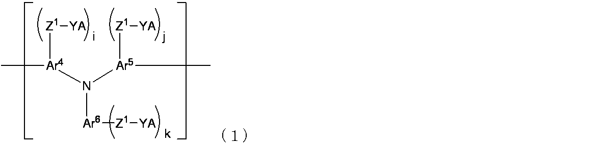
-N+R1R2R3 (2-1)
-P+R1R2R3 (2-2)
-S+R1R2 (2-3)
(式(2-1)、(2-2)及び(2-3)の各々において、R1、R2及びR3はそれぞれ独立に、水素原子、又は置換基を有していてもよい1価の炭化水素基を表し、但し、R1、R2及びR3の少なくとも2個が互いに結合して少なくとも1個の環を形成していてもよい。)
<2>
前記正孔注入及び/又は正孔輸送層が架橋構造を有する上記<1>記載の積層構造体。
また本発明は以下の<3>記載の電子デバイスを提供する。
<3>
上記<1>又は<2>記載の積層構造体を有する電子デバイス。
<3>
上記<1>又は<2>記載の積層構造体を有する電子デバイス。
また本発明は以下の<4>又は<5>記載の芳香族化合物、即ち、カチオン中心を有する基の少なくとも1種を炭化水素側鎖に有する芳香族化合物を提供する。
<4>
下記式(3)で表される構造単位を有する芳香族化合物。
<4>
下記式(3)で表される構造単位を有する芳香族化合物。
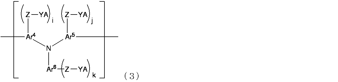
-N+R1R2R3 (2-1)
-P+R1R2R3 (2-2)
-S+R1R2 (2-3)
(式(2-1)、(2-2)及び(2-3)の各々において、R1、R2及びR3はそれぞれ独立に、水素原子、又は置換基を有していてもよい1価の炭化水素基を表し、但し、R1、R2及びR3の少なくとも2個が互いに結合して少なくとも1個の環を形成していてもよい。)
<5>
下記式(4)で表される上記<4>記載の芳香族化合物。

また本発明は以下の<6>又は<7>記載の芳香族化合物、即ち、第1級~第4級のアンモニウムイオンの少なくとも1種を炭化水素側鎖に有する芳香族化合物を提供する。
<6>
下記式(5)で表される構造単位を有する芳香族化合物である上記<4>記載の芳香族化合物。
<6>
下記式(5)で表される構造単位を有する芳香族化合物である上記<4>記載の芳香族化合物。

<7>
下記式(6)で表される上記<6>記載の芳香族化合物。

また本発明は以下の<8>又は<9>記載の芳香族化合物、即ち、脱離基を炭化水素側鎖に有する芳香族化合物を提供する。
<8>
下記式(7)で表される構造単位を有する芳香族化合物。
<8>
下記式(7)で表される構造単位を有する芳香族化合物。
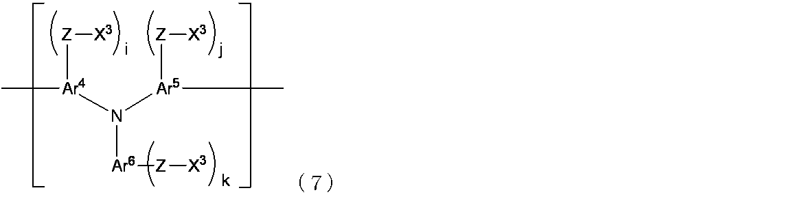
<9>
下記式(8)で表される上記<8>記載の芳香族化合物。

また本発明は以下の<10>又は<11>記載の芳香族化合物、即ち、脱離基を炭化水素側鎖に有する芳香族化合物を提供する。
<10>
下記式(9)で表される構造単位を有する芳香族化合物である上記<8>記載の芳香族化合物。
<10>
下記式(9)で表される構造単位を有する芳香族化合物である上記<8>記載の芳香族化合物。
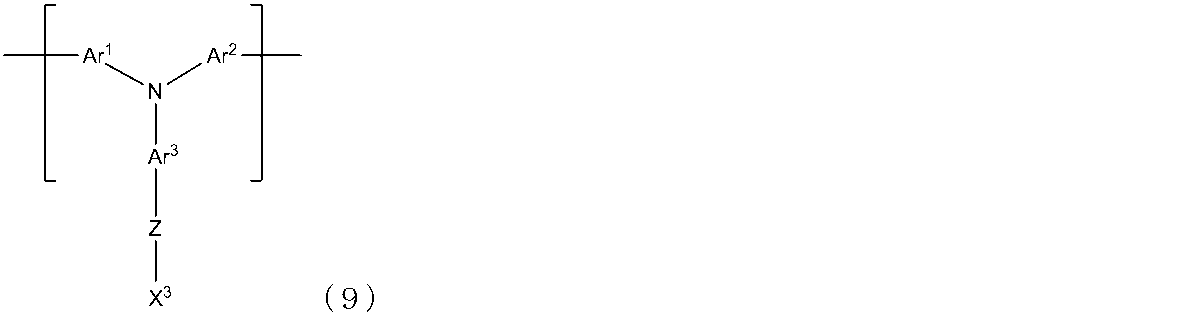
<11>
下記式(10)で表される上記<10>記載の芳香族化合物。
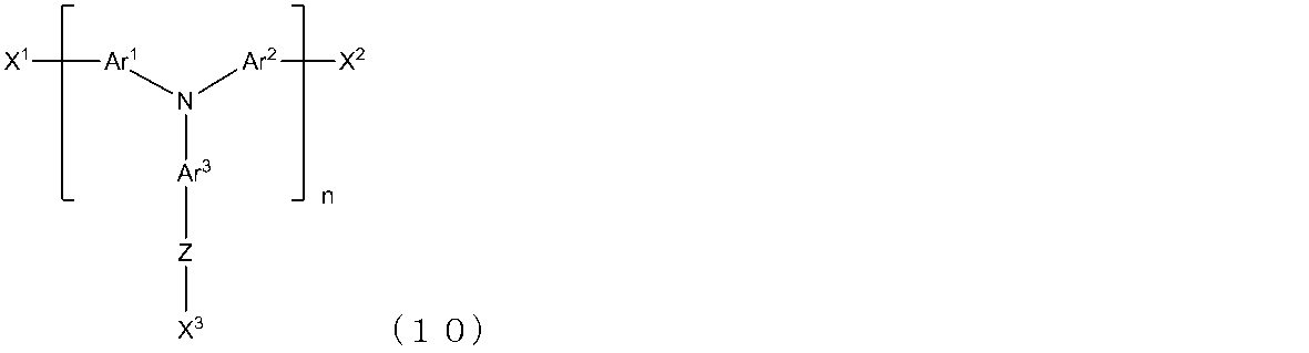
更に、本発明は以下の<12>、<13>又は<14>記載の、芳香族化合物の製造方法を提供する。
<12>
上記<8>記載の式(7)で表される構造単位を有する芳香族化合物を、下記式(11-1)で表される窒素化合物、下記式(11-2)で表されるリン化合物、下記式(11-3)で表される硫黄化合物又はそれら化合物の2種以上の組み合わせと反応させることにより、該芳香族化合物をそのオニウム塩に変換することを含む上記<4>記載の式(3)で表される構造単位を有する芳香族化合物の製造方法。
NR1R2R3 (11-1)
PR1R2R3 (11-2)
SR1R2 (11-3)
(式(11-1)、(11-2)及び(11-3)の各々において、R1、R2及びR3はそれぞれ独立に、水素原子、又は置換基を有していてもよい1価の炭化水素基を表し、但し、R1、R2及びR3の少なくとも2個が互いに結合して少なくとも1個の環を形成していてもよい。)
<13>
式(7)で表される構造単位を有する上記<8>記載の芳香族化合物が式(8)で表される上記<9>記載の芳香族化合物であり、式(3)で表される構造単位を有する上記<5>記載の芳香族化合物が式(4)で表される上記<5>記載の芳香族化合物である上記<12>記載の製造方法。
<14>
式(7)で表される構造単位を有する上記<8>記載の芳香族化合物中のX3で表される脱離基に、前記窒素化合物、前記リン化合物、前記硫黄化合物又はそれら化合物の2種以上の組み合わせを反応させる上記<12>記載の製造方法。
<12>
上記<8>記載の式(7)で表される構造単位を有する芳香族化合物を、下記式(11-1)で表される窒素化合物、下記式(11-2)で表されるリン化合物、下記式(11-3)で表される硫黄化合物又はそれら化合物の2種以上の組み合わせと反応させることにより、該芳香族化合物をそのオニウム塩に変換することを含む上記<4>記載の式(3)で表される構造単位を有する芳香族化合物の製造方法。
NR1R2R3 (11-1)
PR1R2R3 (11-2)
SR1R2 (11-3)
(式(11-1)、(11-2)及び(11-3)の各々において、R1、R2及びR3はそれぞれ独立に、水素原子、又は置換基を有していてもよい1価の炭化水素基を表し、但し、R1、R2及びR3の少なくとも2個が互いに結合して少なくとも1個の環を形成していてもよい。)
<13>
式(7)で表される構造単位を有する上記<8>記載の芳香族化合物が式(8)で表される上記<9>記載の芳香族化合物であり、式(3)で表される構造単位を有する上記<5>記載の芳香族化合物が式(4)で表される上記<5>記載の芳香族化合物である上記<12>記載の製造方法。
<14>
式(7)で表される構造単位を有する上記<8>記載の芳香族化合物中のX3で表される脱離基に、前記窒素化合物、前記リン化合物、前記硫黄化合物又はそれら化合物の2種以上の組み合わせを反応させる上記<12>記載の製造方法。
更に、本発明は以下の<15>又は<16>記載の、芳香族化合物の製造方法を提供する。
<15>
式(9)で表される構造単位を有する上記<10>記載の芳香族化合物中のX3で表される脱離基に、上記式(11-1)で表される窒素化合物を反応させることにより、式(5)で表される構造単位を有する上記<6>記載の芳香族化合物を製造する上記<14>記載の製造方法。
<16>
式(9)で表される構造単位を有する上記<10>記載の芳香族化合物が式(10)で表される上記<11>記載の芳香族化合物であり、式(5)で表される構造単位を有する上記<6>記載の芳香族化合物が式(6)で表される上記<7>記載の芳香族化合物である上記<15>記載の製造方法。
<15>
式(9)で表される構造単位を有する上記<10>記載の芳香族化合物中のX3で表される脱離基に、上記式(11-1)で表される窒素化合物を反応させることにより、式(5)で表される構造単位を有する上記<6>記載の芳香族化合物を製造する上記<14>記載の製造方法。
<16>
式(9)で表される構造単位を有する上記<10>記載の芳香族化合物が式(10)で表される上記<11>記載の芳香族化合物であり、式(5)で表される構造単位を有する上記<6>記載の芳香族化合物が式(6)で表される上記<7>記載の芳香族化合物である上記<15>記載の製造方法。
本発明の芳香族化合物は、電子デバイスに応用でき、とりわけ正孔注入及び/又は正孔
輸送材料として好適に利用でき、同じ電圧でより高い電流密度を確保できる。
輸送材料として好適に利用でき、同じ電圧でより高い電流密度を確保できる。
以下、本発明について、説明する。まず本明細書において汎用される用語について説明する。用語について特に限定されていなければ、以下の定義を用いる。
本明細書において、「置換基を有していてもよい」とは、その直後に記載された化合物又は基を構成する水素原子が無置換の場合および水素原子の一部又は全部が置換基によって置換されている場合の双方を含み、置換基によって置換されている場合には、ハロゲン原子、水酸基、アミノ基、ニトロ基、炭素原子数1~30のヒドロカルビル基、炭素原子数1~30のヒドロカルビルオキシ基等の置換基によって置換されていることを意味し、これらの中でも、ハロゲン原子、炭素原子数1~18のヒドロカルビル基、炭素原子数1~18のヒドロカルビルオキシ基で置換されていることが好ましく、炭素原子数1~12のヒドロカルビル基、炭素原子数1~12のヒドロカルビルオキシ基で置換されていることがより好ましく、炭素原子数1~10のヒドロカルビル基、炭素原子数1~10のヒドロカルビルオキシ基で置換されていることがさらに好ましく、炭素原子数1~6のヒドロカルビル基、炭素原子数1~6のヒドロカルビルオキシ基で置換されていることが特に好ましい。ヒドロカルビル基およびヒドロカルビルオキシ基等の置換基はそれぞれ、直鎖状、分岐鎖状、又は環状のいずれであってもよい。なお、本明細書においては、「置換基を有していてもよい」との表現に代わりに、「置換されていてもよい」又は「置換基を有し又は有しない」と言い換えてもよい。
上記のハロゲン原子としては、例えば、フッ素原子、塩素原子、臭素原子、ヨウ素原子が挙げられ、好ましくは、フッ素原子、塩素原子、臭素原子であり、より好ましくは、フッ素原子、塩素原子である。
上記のヒドロカルビル基は、直鎖状、分岐鎖状又は環状のいずれでもよい。上記のヒドロカルビル基としては、例えば、メチル基、エチル基、1-プロピル基、2-プロピル基、1-ブチル基、2-ブチル基、tert-ブチル基、ペンチル基、ヘキシル基、オクチル基、デシル基、ドデシル基、2-エチルヘキシル基、3,7-ジメチルオクチル基、シクロプロピル基、シクロペンチル基、シクロヘキシル基、1-アダマンチル基、2-アダマンチル基、ノルボルニル基、アンモニウムエチル基、ベンジル基、α,α―ジメチルベンジル基、1-フェネチル基、2-フェネチル基、ビニル基、プロペニル基、ブテニル基、オレイル基、エイコサペンタエニル基、ドコサヘキサエニル基、2,2-ジフェニルビニル基、1,2,2-トリフェニルビニル基、2-フェニル-2-プロペニル基、フェニル基、2-トリル基、4-トリル基、4-トリフルオロメチルフェニル基、4-メトキシフェニル基、4-シアノフェニル基、2-ビフェニリル基、3-ビフェニリル基、4-ビフェニリル基、ターフェニリル基、3,5-ジフェニルフェニル基、3,4-ジフェニルフェニル基、ペンタフェニルフェニル基、4-(2,2-ジフェニルビニル)フェニル基、4-(1,2,2-トリフェニルビニル)フェニル基、フルオレニル基、1-ナフチル基、2-ナフチル基、9-アントリル基、2-アントリル基、9-フェナントリル基、1-ピレニル基、クリセニル基、ナフタセニル基、コロニル基が挙げられ、好ましくはメチル基、エチル基、1-プロピル基、2-プロピル基、1-ブチル基、2-ブチル基、tert-ブチル基、ペンチル基、ヘキシル基、オクチル基、デシル基、ドデシル基、2-エチルヘキシル基、3,7-ジメチルオクチル基、ベンジル基、α,α―ジメチルベンジル基、1-フェネチル基、2-フェネチル基、ビニル基、プロペニル基、ブテニル基、オレイル基、エイコサペンタエニル基、ドコサヘキサエニル基、2,2-ジフェニルビニル基、1,2,2-トリフェニルビニル基、2-フェニル-2-プロペニル基、フェニル基、2-トリル基、4-トリル基、4-トリフルオロメチルフェニル基、4-メトキシフェニル基、4-シアノフェニル基、2-ビフェニリル基、3-ビフェニリル基、4-ビフェニリル基、ターフェニリル基、3,5-ジフェニルフェニル基、3,4-ジフェニルフェニル基、ペンタフェニルフェニル基、4-(2,2-ジフェニルビニル)フェニル基、4-(1,2,2-トリフェニルビニル)フェニル基、フルオレニル基、1-ナフチル基、2-ナフチル基、9-アントリル基、2-アントリル基、9-フェナントリル基であり、より好ましくはメチル基、エチル基、1-プロピル基、2-プロピル基、1-ブチル基、2-ブチル基、tert-ブチル基、ペンチル基、ヘキシル基、オクチル基、2-エチルヘキシル基、3,7-ジメチルオクチル基、ベンジル基、フェニル基であり、さらに好ましくはメチル基、エチル基、1-プロピル基、2-プロピル基、1-ブチル基、2-ブチル基、tert-ブチル基、ペンチル基、ヘキシル基である。
上記のヒドロカルビルオキシ基は、直鎖状、分岐鎖状又は環状のいずれでもよい。上記のヒドロカルビルオキシ基としては、例えば、メトキシ基、エトキシ基、1-プロパノキシ基、2-プロパノキシ基、1-ブトキシ基、2-ブトキシ基、tert-ブトキシ基、ペンチルオキシ基、ヘキシルオキシ基、オクチルオキシ基、デシルオキシ基、ドデシルオキシ基、2-エチルヘキシルオキシ基、3,7-ジメチルオクチルオキシ基、シクロプロパノキシ基、シクロペンチルオキシ基、シクロヘキシルオキシ基、1-アダマンチルオキシ基、2-アダマンチルオキシ基、ノルボルニルオキシ基、アンモニウムエチトキシ基、トリフルオロメトキシ基、ベンジロキシ基、α,α-ジメチルベンジロキシ基、2-フェネチルオキシ基、1-フェネチルオキシ基、フェノキシ基、アルコキシフェノキシ基、アルキルフェノキシ基、1-ナフチルオキシ基、2-ナフチルオキシ基、ペンタフルオロフェニルオキシ基が挙げられ、好ましくはメトキシ基、エトキシ基、1-プロパノキシ基、2-プロパノキシ基、1-ブトキシ基、2-ブトキシ基、tert-ブトキシ基、ペンチルオキシ基、ヘキシルオキシ基、オクチルオキシ基、デシルオキシ基、ドデシルオキシ基、2-エチルヘキシルオキシ基、3,7-ジメチルオクチルオキシ基であり、より好ましくはメトキシ基、エトキシ基、1-プロパノキシ基、2-プロパノキシ基、1-ブトキシ基、2-ブトキシ基、tert-ブトキシ基、ペンチルオキシ基、ヘキシルオキシ基である。
本明細書において、Phはフェニル基を表し、ImはN-イミダゾリル基を表す。
本明細書において、「正孔注入及び/又は正孔輸送材料」とは、正孔注入性及び正孔輸送性のいずれか一方又は両方を有する材料をいう。また、本明細書において、「正孔注入及び/又は正孔輸送層」とは、正孔注入性及び正孔輸送性のいずれか一方又は両方を有する層をいう。
以下、本発明を実施するための一実施形態について説明する。
以下、本発明を実施するための一実施形態について説明する。
本発明は、基体と、下記式(1)で表される構造単位を有する芳香族化合物を含む正孔注入及び/又は正孔輸送層とを有する積層構造体を提供する。

Ar4及びAr5としては、1,3-フェニレン基、1,4-フェニレン基等の単環性芳香族基;ナフタレン-1,3-ジイル基、ナフタレン-1,4-ジイル基、ナフタレン-1,5-ジイル基、ナフタレン-1,6-ジイル基、ナフタレン-1,7-ジイル基、ナフタレン-2,6-ジイル基、ナフタレン-2,7-ジイル基等の縮合環系芳香族基;ピリジン-2,5-ジイル基、ピリジン-2,6-ジイル基、キノキサリン-2,6-ジイル基、チオフェン-2,5-ジイル基等のヘテロ芳香族基等を挙げることができる。これらのなかでも、単環性芳香族基及び縮合環系芳香族基が好ましく、1,3-フェニレン基、1,4-フェニレン基、ナフタレン-1,4-ジイル基、ナフタレン-1,5-ジイル基、ナフタレン-2,6-ジイル基及びナフタレン-2,7-ジイル基からなる群から選ばれるものがより好ましく、1,3-フェニレン基又は1,4-フェニレン基がさらに好ましく、1,4-フェニレン基が特に好ましい。これらの基は置換基を有していてもよい。
Ar6としては、フェニル基、フェニレン基(例えば、1,3-フェニレン基、1,4-フェニレン基)等の単環性芳香族基;ナフタレン-1-イル基、ナフタレン-2-イル基、ナフタレンジイル基(例えば、ナフタレン-1,3-ジイル基、ナフタレン-1,4-ジイル基、ナフタレン-1,5-ジイル基、ナフタレン-1,6-ジイル基、ナフタレン-1,7-ジイル基、ナフタレン-2,6-ジイル基、ナフタレン-2,7-ジイル基)等の縮合環系芳香族基;ピリジン-2,5-ジイル基、ピリジン-2-イル基、キノキサリン-2-イル基、チオフェン-2-イル基等のヘテロ芳香族基等を挙げることができる。これらのなかでも、単環性芳香族基及び縮合環系芳香族基が好ましく、フェニレン基及びナフタレンジイル基からなる群から選ばれるものがより好ましく、フェニレン基がさらに好ましい。これらの基は置換基を有していてもよい。
Z1は2価の基を表す。該2価の基としては、置換されていてもよい2価の炭化水素基が好ましく用いられる。中でも、置換されていてもよい炭素原子数1~50の2価の炭化水素基が好ましく、置換されていてもよい炭素原子数2~40の2価の炭化水素基がより好ましく、溶媒溶解性を確保しやすく素子及びデバイスへの加工性が向上する点から、置換されていてもよい炭素原子数6~30の2価の炭化水素基が更に好ましい。-YAで表される部分の導入効果が大きくなりやすいため、Z1の炭素原子数は50以下であることが好ましい。前記2価の炭化水素基の中では、溶媒溶解性を確保しやすく素子及びデバイスへの加工性が向上しやすい点から、アルキレン基が好ましい。アルキレン基としては直鎖のものが好ましい。
Yは、下記式(2-1)、(2-2)又は(2-3)で表される基であり、カチオン中心を有する1価の基に属する。
-N+R1R2R3 (2-1)
-P+R1R2R3 (2-2)
-S+R1R2 (2-3)
(式(2-1)、(2-2)及び(2-3)の各々において、R1、R2及びR3はそれぞれ独立に、水素原子、又は置換されていてもよい1価の炭化水素基を表し、但し、R1、R2及びR3の少なくとも2個が互いに結合して少なくとも1個の環を形成していてもよい。)
-N+R1R2R3 (2-1)
-P+R1R2R3 (2-2)
-S+R1R2 (2-3)
(式(2-1)、(2-2)及び(2-3)の各々において、R1、R2及びR3はそれぞれ独立に、水素原子、又は置換されていてもよい1価の炭化水素基を表し、但し、R1、R2及びR3の少なくとも2個が互いに結合して少なくとも1個の環を形成していてもよい。)
R1、R2及びR3はそれぞれ独立に、水素原子、又は置換されていてもよい1価の炭化水素基(ヒドロカルビル基)を表し、但し、R1、R2及びR3の少なくとも2個が互いに結合して少なくとも1個の環を形成していてもよい。
該ヒドロカルビル基がアルキル基である場合、炭素原子数1~20であることが好ましく、メチル基、エチル基、n-プロピル基、iso-プロピル基、n-ブチル基、sec-ブチル基、iso-ブチル基、tert-ブチル基、n-ペンチル基、2,2-ジメチルプロピル基、n-ヘキシル基、シクロヘキシル基、n-ヘプチル基、n-オクチル基、n-ノニル基、n-デシル基、n-ウンデシル基、n-ドデシル基、n-トリデシル基、n-テトラデシル基、n-ペンタデシル基、n-ヘキサデシル基、n-ヘプタデシル基、n-オクタデシル基、n-ノナデシル基、n-イコシル基等の直鎖状、分岐鎖状もしくは環状のアルキル基が例示できる。
また、該ヒドロカルビル基がアリール基である場合は、炭素原子数6~20であることが好ましく、フェニル基、1-ナフチル基、2-ナフチル基、3-フェナントリル基、2-アントリル基等が挙げられる。
R1、R2及びR3の少なくとも2個が互いに結合して形成する環は、炭素環若しくは複素環又はその組み合わせであり、該複素環は、Zに結合した窒素原子、リン原子又は硫黄原子のみを含んでもよいし、該窒素原子、リン原子又は硫黄原子以外に窒素原子、酸素原子等のヘテロ原子を含んでもよい。
該ヒドロカルビル基がアルキル基である場合、炭素原子数1~20であることが好ましく、メチル基、エチル基、n-プロピル基、iso-プロピル基、n-ブチル基、sec-ブチル基、iso-ブチル基、tert-ブチル基、n-ペンチル基、2,2-ジメチルプロピル基、n-ヘキシル基、シクロヘキシル基、n-ヘプチル基、n-オクチル基、n-ノニル基、n-デシル基、n-ウンデシル基、n-ドデシル基、n-トリデシル基、n-テトラデシル基、n-ペンタデシル基、n-ヘキサデシル基、n-ヘプタデシル基、n-オクタデシル基、n-ノナデシル基、n-イコシル基等の直鎖状、分岐鎖状もしくは環状のアルキル基が例示できる。
また、該ヒドロカルビル基がアリール基である場合は、炭素原子数6~20であることが好ましく、フェニル基、1-ナフチル基、2-ナフチル基、3-フェナントリル基、2-アントリル基等が挙げられる。
R1、R2及びR3の少なくとも2個が互いに結合して形成する環は、炭素環若しくは複素環又はその組み合わせであり、該複素環は、Zに結合した窒素原子、リン原子又は硫黄原子のみを含んでもよいし、該窒素原子、リン原子又は硫黄原子以外に窒素原子、酸素原子等のヘテロ原子を含んでもよい。
Aは1価又は2価以上のアニオンを表し、但し、2価以上のアニオンである場合、上記構造単位はさらに他のカチオンを有していてもよい。具体的には、フッ化物イオン、塩化物イオン、臭化物イオン、ヨウ化物イオン、硫酸イオン、硝酸イオン、炭酸イオン、酢酸イオン、過塩素酸イオン、テトラフルオロボレートイオン、ヘキサフルオロホスフェートイオン、ヘキサフルオロアンチモンイオン、ヘキサフルオロヒ素イオン、メタンスルホン酸イオン、トリフルオロメタンスルホン酸イオン、トリフルオロ酢酸イオン、ベンゼンスルホン酸イオン、パラトルエンスルホン酸イオン、ドデシルベンゼンスルホン酸イオン、テトラフェニルボレートイオン、テトラキス(ペンタフルオロフェニル)ボレートイオン、テトラ(N-イミダゾリル)ボレートイオン、これらのイオンの構造を有する繰り返し単位を含む高分子化合物等が挙げられる。好ましくはフッ化物イオン、塩化物イオン、臭化物イオン、ヨウ化物イオン、テトラフルオロボレートイオン、ヘキサフルオロホスフェートイオン、トリフルオロメタンスルホン酸イオン、テトラフェニルボレートイオン、テトラ(N-イミダゾリル)ボレートイオンである。
他のカチオンとしては、例えば、リチウムイオン、ナトリウムイオン、カリウムイオンなどのアルカリ金属イオンが挙げられる。また、式(1)で表される一構造単位中の2価以上のアニオンAが、式(1)で表される他の構造単位中のN+、P+、S+などのカチオンと結合することで電荷が打ち消しあっていてもよい。
他のカチオンとしては、例えば、リチウムイオン、ナトリウムイオン、カリウムイオンなどのアルカリ金属イオンが挙げられる。また、式(1)で表される一構造単位中の2価以上のアニオンAが、式(1)で表される他の構造単位中のN+、P+、S+などのカチオンと結合することで電荷が打ち消しあっていてもよい。
i、j及びkはそれぞれ独立に0以上の整数を表す。但し、i+j+kは1以上の整数であり、好ましくは1~6の整数であり、より好ましくは1~3の整数であり、さらに好ましくは1である。
前記式(1)で表される構造単位を有する芳香族化合物における構造単位の合計を100モル%としたとき、前記式(1)で表される構造単位の割合が1モル%以上100モル%以下の範囲であることが好ましく、1モル%以上99モル%以下の範囲であることがより好ましく、5モル%以上90モル%以下の範囲であることがさらに好ましく、10モル%以上80モル%以下の範囲であることが一層好ましく、20モル%以上70モル%以下の範囲であることが特に好ましい。該芳香族化合物は単独重合体であるよりも共重合体であることが好ましい。
上記式(1)の具体例として、以下の構造単位(1a)~(1c)、(1f)、(1g)及び(1i)~(1z)が示される。なお式中、mは1~50の整数を表す。その中でもmは2~40の整数であることが好ましく、2~30の整数であることがより好ましく、6~30であることが更に好ましい。
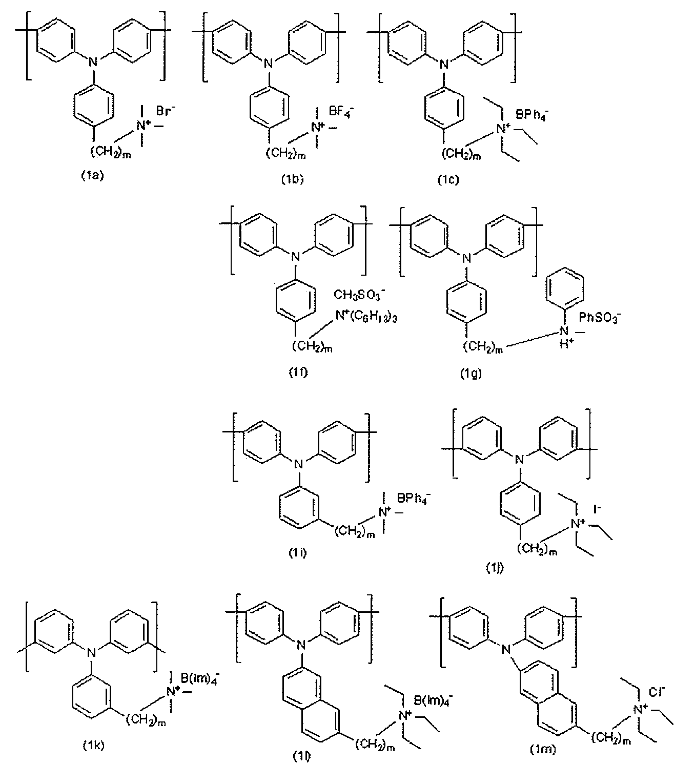

さらに上記式(1)の具体例として、以下の構造単位(1a2)~(1k2)及び(1m2)~(1r2)が示される。mは前記と同じ意味である。
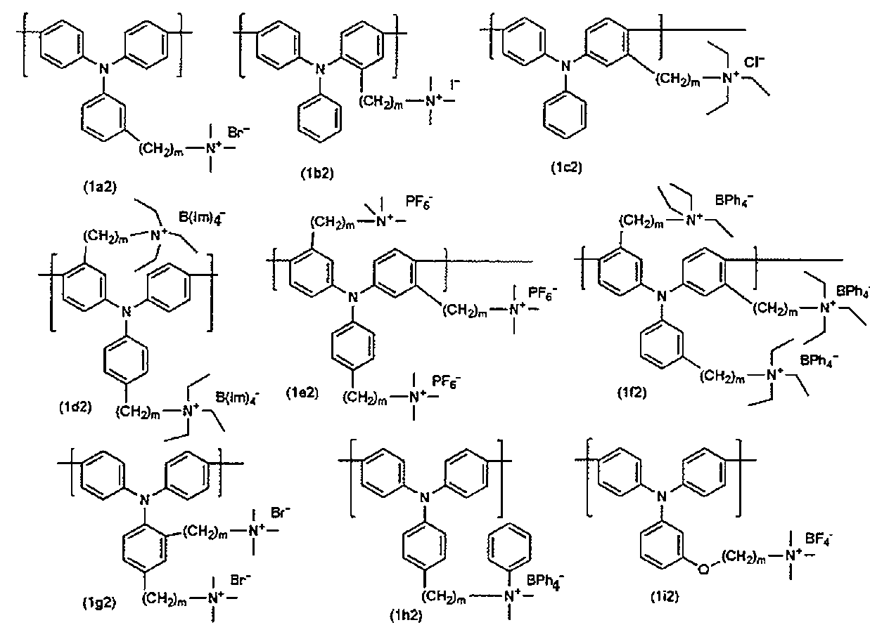

さらに上記式(1)の具体例として、以下の構造単位(1a3)~(1m3)及び(1o3)~(1q3)が示される。なおmは前記と同じ意味である。
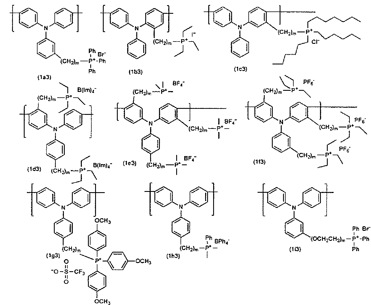

さらに上記式(1)の具体例として、以下の構造単位(1a4)~(1q4)が示される。mは前記と同じ意味である。
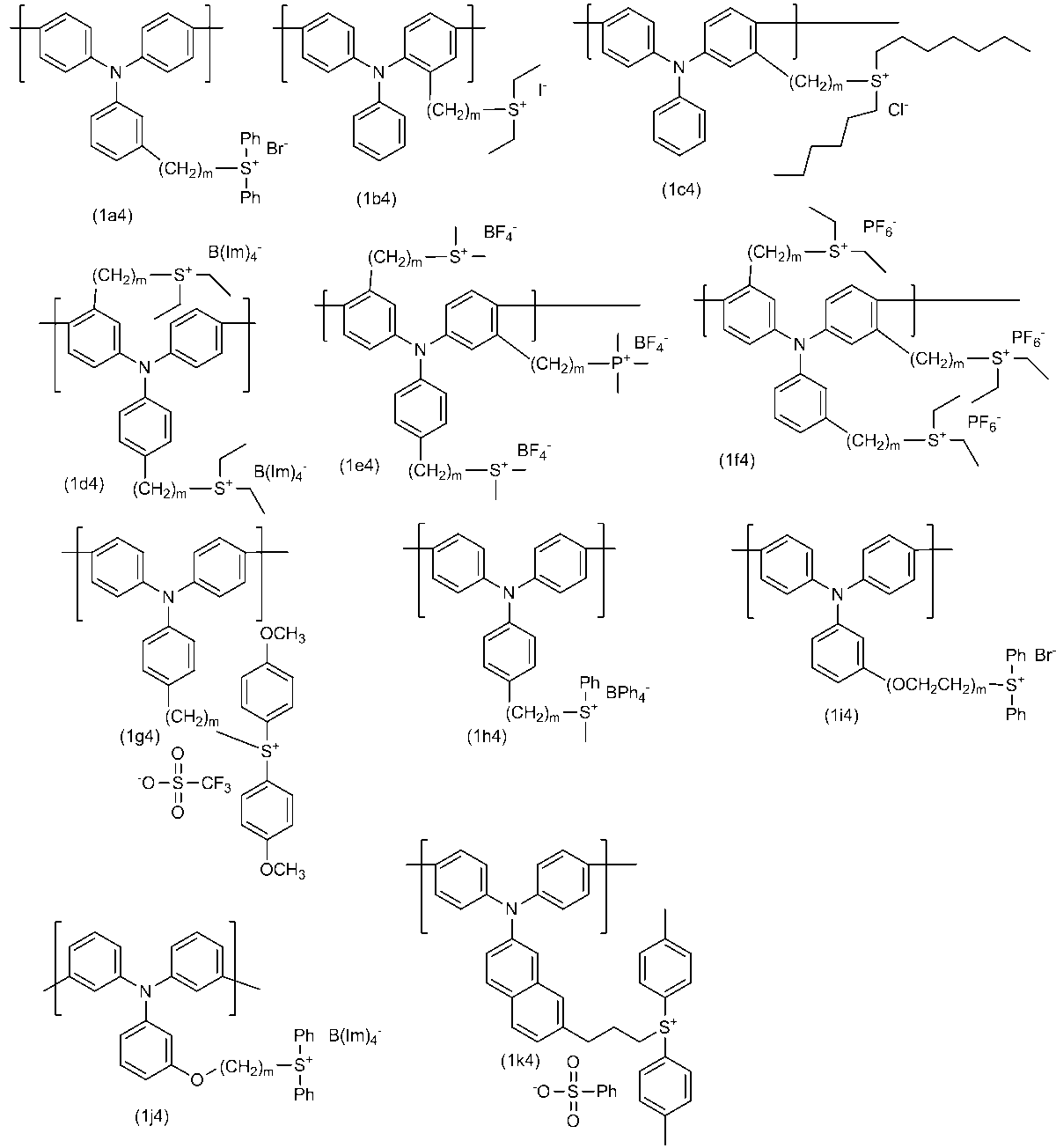

これらの(1a)~(1c)、(1f)、(1g)、(1i)~(1z)、(1a2)~(1k2)、(1m2)~(1r2)、(1a3)~(1m3)、(1o3)~(1q3)、及び(1a4)~(1q4)のうち、極性が高くて高極性溶媒にも溶解しやすい点、及び熱による分解が起こりにくい点から、(1a)~(1c)、(1f)、(1g)、(1i)~(1z)が好ましい。
これらの(1a)~(1c)、(1f)、(1g)、(1i)~(1z)のうちでも、(1a)、(1b)、(1c)、(1l)、(1k)、(1m)、(1n)、(1p)、(1q)、(1r)、(1s)、(1t)、(1v)、(1y)、(1z)が好ましく、(1a)、(1c)、(1l)、(1p)、(1q)、(1r)、(1t)、(1y)、(1z)がより好ましく、(1a)、(1c)、(1r)、(1t)、(1y)がさらに好ましい。
これらの(1a)~(1c)、(1f)、(1g)、(1i)~(1z)のうちでも、(1a)、(1b)、(1c)、(1l)、(1k)、(1m)、(1n)、(1p)、(1q)、(1r)、(1s)、(1t)、(1v)、(1y)、(1z)が好ましく、(1a)、(1c)、(1l)、(1p)、(1q)、(1r)、(1t)、(1y)、(1z)がより好ましく、(1a)、(1c)、(1r)、(1t)、(1y)がさらに好ましい。
また、前記式(1)で表される構造単位を有する芳香族化合物には、繰り返し単位として上記式(1)で表される構造単位の他に、以下の式(12)で表される構造単位を含んでいてもよい。

式(12)において、Ar7としては、1,3-フェニレン基、1,4-フェニレン基等の2価の単環性芳香族基;ナフタレン-1,3-ジイル基、ナフタレン-1,4-ジイル基、ナフタレン-1,5-ジイル基、ナフタレン-1,6-ジイル基、ナフタレン-1,7-ジイル基、ナフタレン-2,6-ジイル基、ナフタレン-2,7-ジイル基等の2価の縮合環系芳香族基;ピリジン-2,5-ジイル基、ピリジン-2,6-ジイル基、キノキサリン-2,6-ジイル基、チオフェン-2,5-ジイル基等の2価のヘテロ芳香族基等を挙げることができる。
式(12)としては、上述した2価の芳香族基からなる構造単位に加えて、以下の式(6a)~(6w)で表される構造単位が挙げられる。このような構造単位を含むことにより、前記式(1)で表される構造単位を有する芳香族化合物の有する正孔注入性がさらに向上しうる。
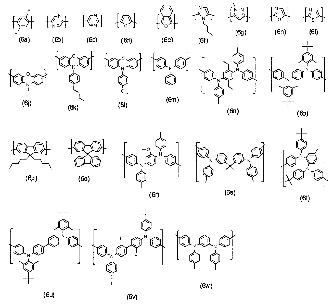
これらのうち、(6a)、(6b)、(6c)、(6f)、(6n)、(6o)、(6t)、(6u)、(6v)、(6w)が好ましく、(6a)、(6b)、(6c)、(6o)、(6t)がより好ましい。
本発明で用いる芳香族化合物を含む正孔注入材料及び/又は正孔輸送材料の利用形態としては、[1]正孔注入層のみに用いる形態、[2]正孔注入層と正孔輸送層の両方に用いる形態、及び[3]正孔輸送層のみに用いる形態、の3種が好ましく挙げられる。
これらのうち、正孔注入層と正孔輸送層の両方に用いる形態が、正極から発光材料への正孔移動がスムーズに行われるため、好ましい。また、正孔注入層と正孔輸送層とを同一の組成とし、1種の材料から同時に作製すれば、正孔注入層と正孔輸送層との界面での抵抗が少なくなる点、及び塗布層が一つ減ることによりプロセスの負荷が軽くなる点から、好ましい。
これらのうち、正孔注入層と正孔輸送層の両方に用いる形態が、正極から発光材料への正孔移動がスムーズに行われるため、好ましい。また、正孔注入層と正孔輸送層とを同一の組成とし、1種の材料から同時に作製すれば、正孔注入層と正孔輸送層との界面での抵抗が少なくなる点、及び塗布層が一つ減ることによりプロセスの負荷が軽くなる点から、好ましい。
本発明で用いる芳香族化合物を含む正孔注入材料及び/又は正孔輸送材料の利用形態としてはさらに、陰極から注入された電子をブロックする機能を有する層としての利用形態も挙げられる。
<積層構造体>
次に、本発明の積層構造体について説明する。本発明の積層構造体は、基体と、式(1)で表される構造単位を有する芳香族化合物を含む正孔注入及び/又は正孔輸送層とを有する。基体としては、例えば、後述の基板が挙げられる。
次に、本発明の積層構造体について説明する。本発明の積層構造体は、基体と、式(1)で表される構造単位を有する芳香族化合物を含む正孔注入及び/又は正孔輸送層とを有する。基体としては、例えば、後述の基板が挙げられる。
<電子デバイス>
本発明の積層構造体を用いる電子デバイスについて説明する。該電子デバイスとしては、例えば、有機トランジスタ、太陽電池などの光電変換素子、電界発光素子等が挙げられる。
本発明の積層構造体を用いる電子デバイスについて説明する。該電子デバイスとしては、例えば、有機トランジスタ、太陽電池などの光電変換素子、電界発光素子等が挙げられる。
<有機トランジスタ>
前記有機トランジスタは、ソース電極、ドレイン電極及び絶縁されたゲート電極層を有するものである。この有機トランジスタは、基板、少なくとも1層の有機層を更に有していてもよい。該有機層の少なくとも1層は、式(1)で表される構造単位を有する芳香族化合物を含む正孔注入及び/又は正孔輸送層である。その際、本発明の積層構造体を用いることができる。
前記有機トランジスタは、ソース電極、ドレイン電極及び絶縁されたゲート電極層を有するものである。この有機トランジスタは、基板、少なくとも1層の有機層を更に有していてもよい。該有機層の少なくとも1層は、式(1)で表される構造単位を有する芳香族化合物を含む正孔注入及び/又は正孔輸送層である。その際、本発明の積層構造体を用いることができる。
<光電変換素子>
前記光電変換素子は、陽極及び陰極からなる電極と、該電極間に設けられた少なくとも1層の有機層とを有するものであって、該有機層の少なくとも1層が電荷分離層であり、該有機層の少なくとも1層が式(1)で表される構造単位を有する芳香族化合物を含む正孔注入及び/又は正孔輸送層であるものである。この光電変換素子は、基板、正孔注入層、電子注入層、正孔輸送層、電子輸送層等を更に有していてもよい。その際、本発明の積層構造体を用いることができる。
前記光電変換素子は、陽極及び陰極からなる電極と、該電極間に設けられた少なくとも1層の有機層とを有するものであって、該有機層の少なくとも1層が電荷分離層であり、該有機層の少なくとも1層が式(1)で表される構造単位を有する芳香族化合物を含む正孔注入及び/又は正孔輸送層であるものである。この光電変換素子は、基板、正孔注入層、電子注入層、正孔輸送層、電子輸送層等を更に有していてもよい。その際、本発明の積層構造体を用いることができる。
<電界発光素子>
本発明の積層構造体を用いる電界発光素子は、例えば、陰極、陽極、前記陰極と前記陽極との間に位置する発光層、及び前記発光層と前記陽極との間に位置し、式(1)で表される構造単位を有する芳香族化合物を含む正孔注入及び/又は正孔輸送層を有する。本発明の電界発光素子は、基板を有することができ、かかる基板の面上に前記陰極、陽極、発光層及び式(1)で表される構造単位を有する芳香族化合物を含む正孔注入及び/又は正孔輸送層、並びに任意の構成要素を設けた構成とすることができる。
本発明の積層構造体を用いる電界発光素子は、例えば、陰極、陽極、前記陰極と前記陽極との間に位置する発光層、及び前記発光層と前記陽極との間に位置し、式(1)で表される構造単位を有する芳香族化合物を含む正孔注入及び/又は正孔輸送層を有する。本発明の電界発光素子は、基板を有することができ、かかる基板の面上に前記陰極、陽極、発光層及び式(1)で表される構造単位を有する芳香族化合物を含む正孔注入及び/又は正孔輸送層、並びに任意の構成要素を設けた構成とすることができる。
本発明の積層構造体を用いる電界発光素子の一態様としては、基板上に陽極が設けられ、その上層に式(1)で表される構造単位を有する芳香族化合物を含む正孔注入及び/又は正孔輸送層が積層され、その上層に発光層が積層され、さらにその上層に陰極が積層される。
他の態様としては、基板上に陽極が設けられ、その上層に式(1)で表される構造単位を有する芳香族化合物を含む正孔注入及び/又は正孔輸送層が積層され、発光層が積層され、その上層に式(1)で表される構造単位を有する芳香族化合物を含む正孔注入及び/又は正孔輸送層が積層され、さらにその上層に陰極が積層される。他の態様としては、陰極を基板上に設け、その上層に式(1)で表される構造単位を有する芳香族化合物を含む正孔注入及び/又は正孔輸送層が積層され、その上層に発光層が積層され、さらにその上層に陽極が積層される。他の態様としては、陰極を基板上に設け、その上層に発光層が積層され、その上層に式(1)で表される構造単位を有する芳香族化合物を含む正孔注入及び/又は正孔輸送層が積層され、さらにその上層に陽極が積層される。さらに他の態様としては、陰極を基板上に設け、その上層に式(1)で表される構造単位を有する芳香族化合物を含む正孔注入及び/又は正孔輸送層が積層され、その上層に発光層が積層され、その上層に式(1)で表される構造単位を有する芳香族化合物を含む正孔注入及び/又は正孔輸送層が積層され、さらにその上層に陽極が積層される。また、これらの態様において、さらに、保護層、バッファー層、反射層等の他の機能を有する層を設けてもよい。なお、本発明の積層構造体を用いる電界発光素子の構成については、下記にて別途詳述する。該電界発光素子はさらに封止膜、或いは、封止基板が覆い被せられ、該電界発光素子が外気と遮断された発光装置が形成される。
式(1)で表される構造単位を有する芳香族化合物を含む正孔注入及び/又は正孔輸送層は、公知の高分子又は低分子の電荷輸送材料、グラフェン、フラーレン、カーボンナノチューブ等の導電性炭素;金属;合金;金属酸化物、金属硫化物等の電気伝導性化合物;及びこれらの混合物等と混合されていてもよい。電荷輸送材料としては、以下の正孔輸送層又は電子輸送層に用いられるものを用いてもよく、金属、合金、金属酸化物、金属硫化物としては、以下の陽極又は陰極に用いられるものを用いてもよい。さらに、発光素子としての発光機能を損なわない範囲で、発光又は電荷輸送機能を有していない有機材料又は金属ハロゲン化物、金属水酸化物、金属炭酸塩等の金属塩、及びこれらの混合物等の無機材料が混合されていてもよい。金属塩としては、仕事関数が3.5eV以下の金属の金属塩であることが好ましく、アルカリ金属又はアルカリ土類金属の金属塩であることがより好ましい。
本発明の積層構造体を用いる電界発光素子は基板側から採光する所謂ボトムエミッションタイプ、基板と反対側から採光する所謂トップエミッションタイプ、両面採光型のいずれのタイプの電界発光素子であってもよい。
式(1)で表される構造単位を有する芳香族化合物を含む正孔注入及び/又は正孔輸送層を形成する方法としては、例えば、式(1)で表される構造単位を有する芳香族化合物を含有する溶液を用いて成膜する方法が挙げられる。
このような溶液を用いる成膜に用いる溶媒としては、アルコール、エーテル、エステル、ニトリル化合物、ニトロ化合物、ハロゲン化アルキル、ハロゲン化アリール、チオール、スルフィド、スルホキシド、チオケトン、アミド、カルボン酸等の水を除く溶媒のうち、溶解度パラメーターが9.3以上の溶媒が好ましい。該溶媒の例(各括弧内の値は、各溶媒の溶解度パラメーターの値を表す。「溶剤ハンドブック(講談社サイエンティフィック、1976年)」P.39に記載の表2.17のσ値から引用。)としては、メタノール(12.9)、エタノール(11.2)、2-プロパノール(11.5)、1-ブタノール(10.7)、tert-ブチルアルコール(10.5)、アセトニトリル(11.8)、1,2-エタンジオール(14.7)、N,N-ジメチルホルムアミド(11.5)、ジメチルスルホキシド(12.8)、酢酸(12.4)、ニトロベンゼン(11.1)、ニトロメタン(11.0)、1,2-ジクロロエタン(9.7)、ジクロロメタン(9.6)、クロロベンゼン(9.6)、ブロモベンゼン(9.9)、ジオキサン(9.8)、炭酸プロピレン(13.3)、ピリジン(10.4)、二硫化炭素(10.0)、及びこれらの溶媒の混合溶媒が挙げられる。ここで、2種の溶媒(溶媒1及び溶媒2とする)を混合してなる混合溶媒について説明すると、該混合溶媒の溶解度パラメーター(δm)は、δm=δ1×φ1+δ2×φ2により求めることとする(δ1は溶媒1の溶解度パラメーター、φ1は溶媒1の体積分率、δ2は溶媒2の溶解度パラメーター、φ2は溶媒2の体積分率である。)
これらの溶媒の中では、防災安全の観点からは、引火点の高い溶媒が好ましく用いられる。
また成膜に用いる溶媒が上記文献に値が掲載されていない場合は、以下の計算によって算出することも出来る。即ち、密度は文献値を用い、その密度に合わせて溶媒分子180個からなるモデルを作成し、力場compassを用いて分子動力学法でNVTアンサンブルにて計算する。十分時間を掛けてエネルギーが平衡状態に達したところで、サンプリングを行い、系の凝集エネルギー密度を計算する(統計量)。溶解度パラメータは凝集エネルギー密度の平方根として求めることができる。
この方法で溶解度パラメータを求めた、以下の溶媒も好ましく用いることが出来る。ジエチレングリコール(14.6)、N,N-ジメチルアセトアミド(11.1)、N-メチルピロリジノン(11.5)である。
なおこれらの溶解度パラメーターの単位は(cal/cm3)1/2である。
これらの溶媒の中では、防災安全の観点からは、引火点の高い溶媒が好ましく用いられる。
また成膜に用いる溶媒が上記文献に値が掲載されていない場合は、以下の計算によって算出することも出来る。即ち、密度は文献値を用い、その密度に合わせて溶媒分子180個からなるモデルを作成し、力場compassを用いて分子動力学法でNVTアンサンブルにて計算する。十分時間を掛けてエネルギーが平衡状態に達したところで、サンプリングを行い、系の凝集エネルギー密度を計算する(統計量)。溶解度パラメータは凝集エネルギー密度の平方根として求めることができる。
この方法で溶解度パラメータを求めた、以下の溶媒も好ましく用いることが出来る。ジエチレングリコール(14.6)、N,N-ジメチルアセトアミド(11.1)、N-メチルピロリジノン(11.5)である。
なおこれらの溶解度パラメーターの単位は(cal/cm3)1/2である。
溶液を用いる成膜方法としては、溶液を用いるスピンコート法、キャスティング法、バーコート法、ロールコート法、ワイアーバーコート法、ディップコート法、スリットコート法、キャピラリーコート法、スプレーコート法、ノズルコート法等のコート法、マイクログラビア印刷法、グラビア印刷法、スクリーン印刷法、フレキソ印刷法、オフセット印刷法、反転印刷法、インクジェットプリント法等の印刷法等の塗布法を用いることができる。パターン形成が容易であるという点で、グラビア印刷法、スクリーン印刷法、フレキソ印刷法、オフセット印刷法、反転印刷法、インクジェットプリント法等の印刷法及びノズルコート法が好ましい。
式(1)で表される構造単位を有する芳香族化合物を含む正孔注入及び/又は正孔輸送層の厚さとしては、用いる材料によって最適値が異なるため、駆動電圧と発光効率が適度な値となるように選択すればよく、ピンホールが発生しない厚さが必要である。素子の駆動電圧を低くする観点からは、該厚さは、1nm~1μmであることが好ましく、2nm~500nmであることがより好ましく、2nm~200nmであることがさらに好ましい。発光層を保護する観点からは、該厚さは、5nm~1μmであることが好ましい。
本発明の積層構造体を用いる電界発光素子は、陰極及び陽極を有し、陰極と陽極間に発光層を有するが、さらに構成要素を備えることができる。
例えば、陽極と発光層との間には式(1)で表される構造単位を有する芳香族化合物を含む正孔注入及び/又は正孔輸送層を有することができる。この場合第1の電極は陽極となり、第2の電極は陰極となる。
例えば、陽極と発光層との間には式(1)で表される構造単位を有する芳香族化合物を含む正孔注入及び/又は正孔輸送層を有することができる。この場合第1の電極は陽極となり、第2の電極は陰極となる。
ここで、陽極は、式(1)で表される構造単位を有する芳香族化合物を含む正孔注入及び/又は正孔輸送層に正孔を供給する電極であり、陰極は、電子注入層、電子輸送層、発光層等に電子を供給する電極である。
発光層とは、電界を印加した際に、陽極側に隣接する層より正孔を受け取り、陰極側に隣接する層より電子を受け取る機能、受け取った電荷(電子と正孔)を電界の力で移動させる機能、及び電子と正孔の再結合の場を提供し、これを発光につなげる機能を有する層をいう。
電子注入層及び電子輸送層とは、陰極から電子を受け取る機能、電子を輸送する機能、陽極から注入された正孔をブロックする機能、及び発光層へ電子を供給する機能のいずれかを有する層をいう。
正孔注入層及び正孔輸送層とは、陽極から正孔を受け取る機能、正孔を輸送する機能、発光層へ正孔を供給する機能、及び陰極から注入された電子をブロックする機能のいずれかを有する層をいう。
なお、電子輸送層と正孔輸送層を総称して電荷輸送層と呼ぶことがある。また、電子注入層と正孔注入層を総称して電荷注入層と呼ぶことがある。
電子注入層及び電子輸送層とは、陰極から電子を受け取る機能、電子を輸送する機能、陽極から注入された正孔をブロックする機能、及び発光層へ電子を供給する機能のいずれかを有する層をいう。
正孔注入層及び正孔輸送層とは、陽極から正孔を受け取る機能、正孔を輸送する機能、発光層へ正孔を供給する機能、及び陰極から注入された電子をブロックする機能のいずれかを有する層をいう。
なお、電子輸送層と正孔輸送層を総称して電荷輸送層と呼ぶことがある。また、電子注入層と正孔注入層を総称して電荷注入層と呼ぶことがある。
即ち、本発明の積層構造体を用いた電界発光素子は下記の層構成(a)を有することができ、又は、層構成(a)から、正孔注入層、正孔輸送層、電子輸送層、電子注入層の1層以上を省略した層構成を有することもできる。層構成(a)において、本発明の芳香族化合物を含む層は、正孔注入層、正孔輸送層、電子注入層、及び電子輸送層からなる群から選ばれる1つ以上の層として用いることができる。
(a)陽極-正孔注入層-(正孔輸送層)-発光層-(電子輸送層)-電子注入層-陰極
ここで、符号「-」は各層が隣接して積層されていることを示す。「(正孔輸送層)」は、正孔輸送層のみからなる層を示す。「(電子輸送層)」は、電子輸送層のみからなる層を示す。以下の層構成の説明においても同様である。
さらに、本発明の積層構造体を用いた電界発光素子は、1つの積層構造中に2層の発光層を有することができる。この場合、該電界発光素子は下記の層構成(b)を有することができ、又は、層構成(b)から、正孔注入層、正孔輸送層、電子輸送層、電子注入層、及び電極の1層以上を省略した層構成を有することもできる。層構成(b)において、式(1)で表される構造単位を有する芳香族化合物を含む正孔注入及び/又は正孔輸送層は、陽極と陽極に最も近い発光層との間に存在する層として用いられるか、陰極と陰極に最も近い発光層との間に存在する層として用いられる。
(b)陽極-正孔注入層-(正孔輸送層)-発光層-(電子輸送層)-電子注入層-電極-正孔注入層-(正孔輸送層)-発光層-(電子輸送層)-電子注入層-陰極
さらに、本発明の積層構造体を用いた電界発光素子は、1つの積層構造中に3層以上の発光層を有することができる。この場合、電界発光素子は下記の層構成(c)を有することができ、又は、層構成(c)から、正孔注入層、正孔輸送層、電子輸送層、電子注入層、及び電極の1層以上を省略した層構成を有することもできる。層構成(c)において、本発明の芳香族化合物を含む層は、陽極と陽極に最も近い発光層との間に存在する層として用いられるか、陰極と陰極に最も近い発光層との間に存在する層として用いられる。
(c)陽極-正孔注入層-(正孔輸送層)-発光層-(電子輸送層)-電子注入層-単位Q-単位Q-・・・-陰極
ここで、「単位Q」は、電極-正孔注入層-(正孔輸送層)-発光層-(電子輸送層)-電子注入層という層構成を示す。
ここで、「単位Q」は、電極-正孔注入層-(正孔輸送層)-発光層-(電子輸送層)-電子注入層という層構成を示す。
本発明において、電荷注入層(電子注入層、正孔注入層)を設けた電界発光素子としては、陰極に隣接して電荷注入層を設けた電界発光素子、陽極に隣接して電荷注入層を設けた電界発光素子が挙げられる。この電界発光素子の層構成としては、以下の(d)~(m)の構成が挙げられる。
(d)陽極-電荷注入層-発光層-陰極
(e)陽極-電荷注入層-発光層-電荷注入層-陰極
(f)陽極-電荷注入層-正孔輸送層-発光層-陰極
(g)陽極-正孔輸送層-発光層-電荷注入層-陰極
(h)陽極-電荷注入層-正孔輸送層-発光層-電荷注入層-陰極
(i)陽極-電荷注入層-発光層-電子輸送層-陰極
(j)陽極-電荷注入層-発光層-電子輸送層-電荷注入層-陰極
(k)陽極-電荷注入層-正孔輸送層-発光層-電子輸送層-陰極
(l)陽極-正孔輸送層-発光層-電子輸送層-電荷注入層-陰極
(m)陽極-電荷注入層-正孔輸送層-発光層-電子輸送層-電荷注入層-陰極
(d)陽極-電荷注入層-発光層-陰極
(e)陽極-電荷注入層-発光層-電荷注入層-陰極
(f)陽極-電荷注入層-正孔輸送層-発光層-陰極
(g)陽極-正孔輸送層-発光層-電荷注入層-陰極
(h)陽極-電荷注入層-正孔輸送層-発光層-電荷注入層-陰極
(i)陽極-電荷注入層-発光層-電子輸送層-陰極
(j)陽極-電荷注入層-発光層-電子輸送層-電荷注入層-陰極
(k)陽極-電荷注入層-正孔輸送層-発光層-電子輸送層-陰極
(l)陽極-正孔輸送層-発光層-電子輸送層-電荷注入層-陰極
(m)陽極-電荷注入層-正孔輸送層-発光層-電子輸送層-電荷注入層-陰極
上記電界発光素子は、さらに電極との密着性向上及び電極からの電荷(即ち正孔又は電子)の注入の改善のために、電極に隣接して絶縁層を設けてもよく、また、界面の密着性向上や混合の防止等のために電荷輸送層(即ち正孔輸送層又は電子輸送層)又は発光層の界面に薄いバッファー層を挿入してもよい。積層する層の順番及び数、並びに各層の厚さについては、発光効率及び素子寿命を勘案して用いることができる。
次に、本発明の積層構造体を用いた電界発光素子を構成する各層の材料及び形成方法について、より詳しく説明する。
-基板-
上記電界発光素子を構成する基板は、電極を形成し、有機層を形成する際に化学的に変化しないものであればよく、例えば、ガラス、プラスチック、高分子フィルム、金属フィルム、シリコン基板、これらを積層した基板が用いられる。前記基板としては、市販のものが入手可能であり、又は公知の方法により製造することができる。
本発明の電界発光素子がディスプレイ装置の画素を構成する際には、当該基板上に画素駆動用の回路が設けられていてもよいし、当該駆動回路上に平坦化膜が設けられていてもよい。平坦化膜が設けられる場合には、該平坦化膜の中心線平均粗さ(Ra)がRa<10nmを満たすことが好ましい。
Raは、日本工業規格JISのJIS-B0601-2001に基づいて、JIS-B0651からJIS-B0656及びJIS-B0671-1等を参考に計測できる。
上記電界発光素子を構成する基板は、電極を形成し、有機層を形成する際に化学的に変化しないものであればよく、例えば、ガラス、プラスチック、高分子フィルム、金属フィルム、シリコン基板、これらを積層した基板が用いられる。前記基板としては、市販のものが入手可能であり、又は公知の方法により製造することができる。
本発明の電界発光素子がディスプレイ装置の画素を構成する際には、当該基板上に画素駆動用の回路が設けられていてもよいし、当該駆動回路上に平坦化膜が設けられていてもよい。平坦化膜が設けられる場合には、該平坦化膜の中心線平均粗さ(Ra)がRa<10nmを満たすことが好ましい。
Raは、日本工業規格JISのJIS-B0601-2001に基づいて、JIS-B0651からJIS-B0656及びJIS-B0671-1等を参考に計測できる。
-陽極-
上記電界発光素子を構成する陽極は、正孔注入層、正孔輸送層、発光層等で用いられる有機半導体材料への正孔供給性の観点から、かかる陽極の発光層側表面の仕事関数が4.0eV以上であることが好ましい。
陽極の材料には、金属、合金、金属酸化物、金属硫化物等の電気伝導性化合物、及びこれらの混合物等を用いることができる。具体的には、酸化錫、酸化亜鉛、酸化インジウム、酸化インジウムスズ(ITO)、酸化インジウム亜鉛(IZO)、酸化モリブデン等の導電性金属酸化物、及び、金、銀、クロム、ニッケル等の金属、これらの導電性金属酸化物と金属との混合物等が挙げられる。
前記陽極は、これら材料の1種又は2種以上からなる単層構造であってもよいし、同一組成又は異種組成の複数層からなる多層構造であってもよい。多層構造である場合は、仕事関数が4.0eV以上である材料を発光層側の最表面層に用いることがより好ましい。
上記電界発光素子を構成する陽極は、正孔注入層、正孔輸送層、発光層等で用いられる有機半導体材料への正孔供給性の観点から、かかる陽極の発光層側表面の仕事関数が4.0eV以上であることが好ましい。
陽極の材料には、金属、合金、金属酸化物、金属硫化物等の電気伝導性化合物、及びこれらの混合物等を用いることができる。具体的には、酸化錫、酸化亜鉛、酸化インジウム、酸化インジウムスズ(ITO)、酸化インジウム亜鉛(IZO)、酸化モリブデン等の導電性金属酸化物、及び、金、銀、クロム、ニッケル等の金属、これらの導電性金属酸化物と金属との混合物等が挙げられる。
前記陽極は、これら材料の1種又は2種以上からなる単層構造であってもよいし、同一組成又は異種組成の複数層からなる多層構造であってもよい。多層構造である場合は、仕事関数が4.0eV以上である材料を発光層側の最表面層に用いることがより好ましい。
陽極の作製方法としては、公知の方法が利用でき、真空蒸着法、スパッタリング法、イオンプレーティング法、メッキ法、溶液を用いる成膜による方法(高分子バインダーとの混合溶液を用いてもよい)等が挙げられる。
陽極の厚さは、通常10nm~10μmであり、好ましくは50nm~500nmである。また、短絡等の電気的接続の不良を防止する観点から、陽極の発光層側表面の中心線平均粗さ(Ra)はRa<10nmを満たすこと好ましく、Ra<5nmを満たすことがより好ましい。
さらに、該陽極は上記方法にて作製された後に、UVオゾン、シランカップリング剤、2,3,5,6-テトラフルオロ-7,7,8,8-テトラシアノキノジメタン等の電子受容性化合物を含む溶液等で表面処理を施されることがある。表面処理によって該陽極に接する層との電気的接続が改善される。
上記電界発光素子において陽極を光反射電極として用いる場合には、かかる陽極が、高光反射性金属からなる光反射層と4.0eV以上の仕事関数を有する材料を含む高仕事関数材料層を組み合わせた多層構造が好ましい。
このような陽極の構成としては、
(i) Ag-MoO3
(ii)(Ag-Pd-Cu合金)-(ITO及び/又はIZO)
(iii)(Al-Nd合金)-(ITO及び/又はIZO)
(iv)(Mo-Cr合金)-(ITO及び/又はIZO)
(v) (Ag-Pd-Cu合金)-(ITO及び/又はIZO)-MoO3
が例示される。十分な光反射率を得る為に、Al、Ag、Al合金、Ag合金、Cr合金等の高光反射性金属層の厚さは50nm以上であることが好ましく、80nm以上であることがより好ましい。ITO、IZO、MoO3等の高仕事関数材料層の厚さは通常、5nm~500nmの範囲である。
このような陽極の構成としては、
(i) Ag-MoO3
(ii)(Ag-Pd-Cu合金)-(ITO及び/又はIZO)
(iii)(Al-Nd合金)-(ITO及び/又はIZO)
(iv)(Mo-Cr合金)-(ITO及び/又はIZO)
(v) (Ag-Pd-Cu合金)-(ITO及び/又はIZO)-MoO3
が例示される。十分な光反射率を得る為に、Al、Ag、Al合金、Ag合金、Cr合金等の高光反射性金属層の厚さは50nm以上であることが好ましく、80nm以上であることがより好ましい。ITO、IZO、MoO3等の高仕事関数材料層の厚さは通常、5nm~500nmの範囲である。
-正孔注入層-
本発明の積層構造体を用いる電界発光素子において、式(1)で表される構造単位を有する芳香族化合物以外の正孔注入層を形成する材料としては、カルバゾール誘導体、トリアゾール誘導体、オキサゾール誘導体、オキサジアゾール誘導体、イミダゾール誘導体、フルオレン誘導体、ポリアリールアルカン誘導体、ピラゾリン誘導体、ピラゾロン誘導体、フェニレンジアミン誘導体、アリールアミン誘導体、スターバースト型アミン、フタロシアニン誘導体、アミノ置換カルコン誘導体、スチリルアントラセン誘導体、フルオレノン誘導体、ヒドラゾン誘導体、スチルベン誘導体、シラザン誘導体、芳香族第三級アミン化合物、スチリルアミン化合物、芳香族ジメチリディン系化合物、ポルフィリン系化合物、ポリシラン系化合物、ポリ(N-ビニルカルバゾール)誘導体、有機シラン誘導体、及びこれらを含む重合体;酸化バナジウム、酸化タンタル、酸化タングステン、酸化モリブデン、酸化ルテニウム、酸化アルミニウム等の導電性金属酸化物;ポリアニリン、アニリン系共重合体、チオフェンオリゴマー、ポリチオフェン等の導電性高分子及びオリゴマー;ポリ(3,4-エチレンジオキシチオフェン)・ポリスチレンスルホン酸、ポリピロール等の有機導電性材料及びこれらを含む重合体;アモルファスカーボン;テトラシアノキノジメタン誘導体(例えば、2,3,5,6-テトラフルオロ-7,7,8,8-テトラシアノキノジメタン)、1,4-ナフトキノン誘導体、ジフェノキノン誘導体、ポリニトロ化合物等のアクセプター性有機化合物;オクタデシルトリメトキシシラン等のシランカップリング剤が好適に使用できる。
前記材料は単一の成分で用いても複数の成分からなる組成物として用いてもよい。また、前記正孔注入層は、前記材料のみからなる単層構造であってもよいし、同一組成又は異種組成の複数層からなる多層構造であってもよい。また、正孔輸送層で用いることができる材料として例示する材料も正孔注入層で用いることができる。
本発明の積層構造体を用いる電界発光素子において、式(1)で表される構造単位を有する芳香族化合物以外の正孔注入層を形成する材料としては、カルバゾール誘導体、トリアゾール誘導体、オキサゾール誘導体、オキサジアゾール誘導体、イミダゾール誘導体、フルオレン誘導体、ポリアリールアルカン誘導体、ピラゾリン誘導体、ピラゾロン誘導体、フェニレンジアミン誘導体、アリールアミン誘導体、スターバースト型アミン、フタロシアニン誘導体、アミノ置換カルコン誘導体、スチリルアントラセン誘導体、フルオレノン誘導体、ヒドラゾン誘導体、スチルベン誘導体、シラザン誘導体、芳香族第三級アミン化合物、スチリルアミン化合物、芳香族ジメチリディン系化合物、ポルフィリン系化合物、ポリシラン系化合物、ポリ(N-ビニルカルバゾール)誘導体、有機シラン誘導体、及びこれらを含む重合体;酸化バナジウム、酸化タンタル、酸化タングステン、酸化モリブデン、酸化ルテニウム、酸化アルミニウム等の導電性金属酸化物;ポリアニリン、アニリン系共重合体、チオフェンオリゴマー、ポリチオフェン等の導電性高分子及びオリゴマー;ポリ(3,4-エチレンジオキシチオフェン)・ポリスチレンスルホン酸、ポリピロール等の有機導電性材料及びこれらを含む重合体;アモルファスカーボン;テトラシアノキノジメタン誘導体(例えば、2,3,5,6-テトラフルオロ-7,7,8,8-テトラシアノキノジメタン)、1,4-ナフトキノン誘導体、ジフェノキノン誘導体、ポリニトロ化合物等のアクセプター性有機化合物;オクタデシルトリメトキシシラン等のシランカップリング剤が好適に使用できる。
前記材料は単一の成分で用いても複数の成分からなる組成物として用いてもよい。また、前記正孔注入層は、前記材料のみからなる単層構造であってもよいし、同一組成又は異種組成の複数層からなる多層構造であってもよい。また、正孔輸送層で用いることができる材料として例示する材料も正孔注入層で用いることができる。
正孔注入層の成膜方法としては、以下の方法が挙げられる。即ち、溶液を用いる成膜方法としては、スピンコート法、キャスティング法、バーコート法、スリットコート法、スプレーコート法、ノズルコート法、グラビア印刷法、スクリーン印刷法、フレキソ印刷法、インクジェットプリント法等の塗布法及び印刷法が挙げられ、昇華性化合物材料を用いる場合には、真空蒸着法、転写法等が挙げられる。溶液を用いる成膜に用いる溶媒としては、式(1)で表される構造単位を有する芳香族化合物を含有する溶液を用いて成膜する方法の説明中で例示した溶媒が挙げられる。
正孔注入層に続いて、正孔輸送層、発光層等の有機化合物層を形成する場合、特に、両方の層を塗布法によって形成する場合には、先に塗布した層が後から塗布する層の溶液に含まれる溶媒に溶解して積層構造を作製できなくなることがある。この場合には、下層を溶媒不溶化する方法を用いることができる。溶媒不溶化する方法としては、高分子化合物に架橋基を付け、架橋させて不溶化する方法、芳香族ビスアジドに代表される芳香環を有する架橋基を持った低分子化合物を架橋剤として混合し、架橋させて不溶化する方法、アクリレート基に代表される芳香環を有しない架橋基を持った低分子化合物を架橋剤として混合し、架橋させて不溶化する方法、下層を紫外光に感光させて架橋させ、上層の製造に用いる有機溶媒に対して不溶化する方法、下層を加熱して架橋させ、上層の製造に用いる有機溶媒に対して不溶化する方法等が挙げられる。下層を加熱する場合の加熱の温度は通常100℃~300℃であり、時間は通常1分~1時間である。
また、架橋以外で下層を溶解させずに積層するその他の方法として、隣り合った層の製造に異なる極性の溶液を用いる方法があり、たとえば、下層に水溶性の高分子化合物を用い、上層に油溶性の高分子化合物を用いて、塗布しても下層が溶解しないようにする方法等がある。
また、架橋以外で下層を溶解させずに積層するその他の方法として、隣り合った層の製造に異なる極性の溶液を用いる方法があり、たとえば、下層に水溶性の高分子化合物を用い、上層に油溶性の高分子化合物を用いて、塗布しても下層が溶解しないようにする方法等がある。
正孔注入層の厚さとしては、用いる材料によって最適値が異なり、駆動電圧と発光効率が適度な値となるように選択すればよいが、ピンホールが発生しない厚さが必要であり、あまり厚いと、素子の駆動電圧が高くなり好ましくない。従って、該正孔注入層の厚さは、通常、1nm~1μmであり、好ましくは2nm~500nmであり、さらに好ましくは10nm~100nmである。
-正孔輸送層-
本発明の電界発光素子において、式(1)で表される構造単位を有する芳香族化合物以外の正孔輸送層を構成する材料としては、例えば、カルバゾール誘導体、トリアゾール誘導体、オキサゾール誘導体、オキサジアゾール誘導体、イミダゾール誘導体、フルオレン誘導体、ポリアリールアルカン誘導体、ピラゾリン誘導体、ピラゾロン誘導体、フェニレンジアミン誘導体、アリールアミン誘導体、アミノ置換カルコン誘導体、スチリルアントラセン誘導体、フルオレノン誘導体、ヒドラゾン誘導体、スチルベン誘導体、シラザン誘導体、芳香族第三級アミン化合物、スチリルアミン化合物、芳香族ジメチリディン系化合物、ポルフィリン系化合物、ポリシラン系化合物、ポリ(N-ビニルカルバゾール)誘導体、有機シラン誘導体、及びこれらの構造を含む重合体;アニリン系共重合体、チオフェンオリゴマー、ポリチオフェン等の導電性高分子及びオリゴマー;ポリピロール等の有機導電性材料が挙げられる。
前記材料は単成分であっても或いは複数の成分からなる組成物であってもよい。また、前記正孔輸送層は、前記材料のみからなる単層構造であってもよいし、同一組成又は異種組成の複数層からなる多層構造であってもよい。また、正孔注入層で用いることができる材料として例示する材料も正孔輸送層で用いることができる。
本発明の電界発光素子において、式(1)で表される構造単位を有する芳香族化合物以外の正孔輸送層を構成する材料としては、例えば、カルバゾール誘導体、トリアゾール誘導体、オキサゾール誘導体、オキサジアゾール誘導体、イミダゾール誘導体、フルオレン誘導体、ポリアリールアルカン誘導体、ピラゾリン誘導体、ピラゾロン誘導体、フェニレンジアミン誘導体、アリールアミン誘導体、アミノ置換カルコン誘導体、スチリルアントラセン誘導体、フルオレノン誘導体、ヒドラゾン誘導体、スチルベン誘導体、シラザン誘導体、芳香族第三級アミン化合物、スチリルアミン化合物、芳香族ジメチリディン系化合物、ポルフィリン系化合物、ポリシラン系化合物、ポリ(N-ビニルカルバゾール)誘導体、有機シラン誘導体、及びこれらの構造を含む重合体;アニリン系共重合体、チオフェンオリゴマー、ポリチオフェン等の導電性高分子及びオリゴマー;ポリピロール等の有機導電性材料が挙げられる。
前記材料は単成分であっても或いは複数の成分からなる組成物であってもよい。また、前記正孔輸送層は、前記材料のみからなる単層構造であってもよいし、同一組成又は異種組成の複数層からなる多層構造であってもよい。また、正孔注入層で用いることができる材料として例示する材料も正孔輸送層で用いることができる。
前記正孔輸送層を構成する材料としては、特開昭63-70257号公報、特開昭63-175860号公報、特開平2-135359号公報、特開平2-135361号公報、特開平2-209988号公報、特開平3-37992号公報、特開平3-152184号公報、特開平5-263073号公報、特開平6-1972号公報、WO2005/52027、特開2006-295203号公報等に開示される化合物も有用であるが、これらの中でも、繰り返し単位として2価の芳香族アミン残基を含む重合体が、好適に用いられる。
正孔輸送層の成膜方法としては、正孔注入層の成膜と同様の方法が挙げられる。溶液を用いる成膜に用いる溶媒としては、正孔注入層の成膜方法で例示した溶媒が挙げられる。
正孔輸送層に続いて、発光層等の有機層を塗布法にて形成する際に、下層が後から塗布する層の溶液に含まれる溶媒に溶解する場合は、正孔注入層の成膜方法での例示と同様の方法で下層を溶媒不溶にすることができる。
正孔輸送層の厚さは、用いる材料によって最適値が異なり、駆動電圧と発光効率が適度な値となるように選択すればよいが、ピンホールが発生しない厚さが必要であり、あまり厚いと、素子の駆動電圧が高くなり好ましくない。従って、該正孔輸送層及びインターレイヤーの厚さは、通常、1nm~1μmであり、好ましくは2nm~500nmであり、さらに好ましくは5nm~100nmである。
-発光層-
上記電界発光素子において、発光層が高分子化合物を含む場合、該高分子化合物としては、ポリフルオレン誘導体、ポリパラフェニレンビニレン誘導体、ポリフェニレン誘導体、ポリパラフェニレン誘導体、ポリチオフェン誘導体、ポリジアルキルフルオレン、ポリフルオレンベンゾチアジアゾール、ポリアルキルチオフェン等の共役高分子化合物を好適に用いることができる。
また、前記高分子化合物を含む発光層は、ペリレン系色素、クマリン系色素、ローダミン系色素等の高分子系色素化合物や、ルブレン、ペリレン、9,10-ジフェニルアントラセン、テトラフェニルブタジエン、ナイルレッド、クマリン6、キナクリドン等の低分子色素化合物を含有してもよい。また、該発光層は、ナフタレン誘導体、アントラセン及びその誘導体、ペリレン及びその誘導体、ポリメチン系、キサンテン系、クマリン系、シアニン系等の色素類、8-ヒドロキシキノリン及びその誘導体の金属錯体、芳香族アミン、テトラフェニルシクロペンタジエン及びその誘導体、並びにテトラフェニルブタジエン及びその誘導体、トリス(2-フェニルピリジン)イリジウム等の燐光を発光する金属錯体を含有してもよい。
上記電界発光素子において、発光層が高分子化合物を含む場合、該高分子化合物としては、ポリフルオレン誘導体、ポリパラフェニレンビニレン誘導体、ポリフェニレン誘導体、ポリパラフェニレン誘導体、ポリチオフェン誘導体、ポリジアルキルフルオレン、ポリフルオレンベンゾチアジアゾール、ポリアルキルチオフェン等の共役高分子化合物を好適に用いることができる。
また、前記高分子化合物を含む発光層は、ペリレン系色素、クマリン系色素、ローダミン系色素等の高分子系色素化合物や、ルブレン、ペリレン、9,10-ジフェニルアントラセン、テトラフェニルブタジエン、ナイルレッド、クマリン6、キナクリドン等の低分子色素化合物を含有してもよい。また、該発光層は、ナフタレン誘導体、アントラセン及びその誘導体、ペリレン及びその誘導体、ポリメチン系、キサンテン系、クマリン系、シアニン系等の色素類、8-ヒドロキシキノリン及びその誘導体の金属錯体、芳香族アミン、テトラフェニルシクロペンタジエン及びその誘導体、並びにテトラフェニルブタジエン及びその誘導体、トリス(2-フェニルピリジン)イリジウム等の燐光を発光する金属錯体を含有してもよい。
また、上記の電界発光素子が有する発光層は、非共役高分子化合物と前記有機色素や前記金属錯体等の発光性有機化合物との組成物から構成されてもよい。非共役高分子化合物としては、ポリエチレン、ポリ塩化ビニル、ポリカーボネート、ポリスチレン、ポリメチルメタクリレート、ポリブチルメタクリレート、ポリエステル、ポリスルホン、ポリフェニレンオキシド、ポリブタジエン、ポリ(N-ビニルカルバゾール)、炭化水素樹脂、ケトン樹脂、フェノキシ樹脂、ポリアミド、エチルセルロース、酢酸ビニル、ABS樹脂、ポリウレタン、メラミン樹脂、不飽和ポリエステル樹脂、アルキド樹脂、エポキシ樹脂、シリコン樹脂が挙げられる。前記の非共役高分子化合物は側鎖にカルバゾール誘導体、トリアゾール誘導体、オキサゾール誘導体、オキサジアゾール誘導体、イミダゾール誘導体、フルオレン誘導体、ポリアリールアルカン誘導体、ピラゾリン誘導体、ピラゾロン誘導体、フェニレンジアミン誘導体、アリールアミン誘導体、アミノ置換カルコン誘導体、スチリルアントラセン誘導体、フルオレノン誘導体、ヒドラゾン誘導体、スチルベン誘導体、シラザン誘導体、芳香族第三級アミン化合物、スチリルアミン化合物、芳香族ジメチリディン化合物、ポルフィリン化合物、及び有機シラン誘導体からなる群から選ばれる1つ以上の誘導体若しくは化合物の構造を有していてもよい。
発光層が低分子化合物を含む場合、該低分子化合物としては、ルブレン、ペリレン、9,10-ジフェニルアントラセン、テトラフェニルブタジエン、ナイルレッド、クマリン6、カルバゾール、キナクリドン等の低分子色素化合物、ナフタレン誘導体、アントラセン及びその誘導体、ペリレン及びその誘導体、ポリメチン系、キサンテン系、クマリン系、シアニン系、インジゴ系等の色素類、8-ヒドロキシキノリン及びその誘導体の金属錯体、フタロシアニン及びその誘導体の金属錯体、芳香族アミン、テトラフェニルシクロペンタジエン及びその誘導体、並びにテトラフェニルブタジエン及びその誘導体等が挙げられる。
発光層が燐光を発光する金属錯体を含む場合、該金属錯体としては、トリス(2-フェニルピリジン)イリジウム、チエニルピリジン配位子含有イリジウム錯体、フェニルキノリン配位子含有イリジウム錯体、トリアザシクロノナン骨格含有テルビウム錯体等が挙げられる。
発光層が燐光を発光する金属錯体を含む場合、該金属錯体としては、トリス(2-フェニルピリジン)イリジウム、チエニルピリジン配位子含有イリジウム錯体、フェニルキノリン配位子含有イリジウム錯体、トリアザシクロノナン骨格含有テルビウム錯体等が挙げられる。
発光層に用いられる高分子化合物としては、WO97/09394、WO98/27136、WO99/54385、WO00/22027、WO01/19834、GB2340304A、GB2348316、US573636、US5741921、US5777070、EP0707020、特開平9-111233号公報、特開平10-324870号公報、特開2000-80167号公報、特開2001-123156号公報、特開2004-168999号公報、特開2007-162009号公報、「有機EL素子の開発と構成材料」(シーエムシー出版、2006年発行)等に開示されているポリフルオレン、その誘導体及び共重合体、ポリアリーレン、その誘導体及び共重合体、ポリアリーレンビニレン、その誘導体及び共重合体、芳香族アミン及びその誘導体の(共)重合体が例示される。
また、低分子化合物としては、特開昭57-51781号公報、「有機薄膜仕事関数データ集[第2版]」(シーエムシー出版、2006年発行)、「有機EL素子の開発と構成材料」(シーエムシー出版、2006年発行)等に記載されている化合物が例示される。
前記材料は単成分であっても或いは複数の成分からなる組成物であってもよい。また、前記発光層は、前記材料の1種又は2種以上からなる単層構造であってもよいし、同一組成又は異種組成の複数層からなる多層構造であってもよい。
また、低分子化合物としては、特開昭57-51781号公報、「有機薄膜仕事関数データ集[第2版]」(シーエムシー出版、2006年発行)、「有機EL素子の開発と構成材料」(シーエムシー出版、2006年発行)等に記載されている化合物が例示される。
前記材料は単成分であっても或いは複数の成分からなる組成物であってもよい。また、前記発光層は、前記材料の1種又は2種以上からなる単層構造であってもよいし、同一組成又は異種組成の複数層からなる多層構造であってもよい。
発光層の成膜方法としては、正孔注入層の成膜と同様の方法が挙げられる。溶液を用いる成膜に用いる溶媒としては、正孔注入層の成膜方法で例示した溶媒が挙げられる。
発光層に続いて、電子輸送層等の有機化合物層を塗布法にて形成する際に、下層が後から塗布する層の溶液に含まれる溶媒に溶解する場合は、正孔注入層の成膜方法での例示と同様の方法で下層を溶媒不溶にすることができる。
発光層の厚さとしては、用いる材料によって最適値が異なり、駆動電圧と発光効率が適度な値となるように選択すればよいが、ピンホールが発生しない厚さが必要であり、あまり厚いと、素子の駆動電圧が高くなり好ましくない。従って、発光層の厚さは、通常、5nm~1μmであり、好ましくは10nm~500nmであり、さらに好ましくは30nm~200nmである。
-電子輸送層-
上記電界発光素子において、式(1)で表される構造単位を有する芳香族化合物以外の電子輸送層及び正孔ブロック層を構成する材料としては、公知のものが使用でき、トリアゾール誘導体、オキサゾール誘導体、オキサジアゾール誘導体、イミダゾール誘導体、フルオレン誘導体、ベンゾキノン及びその誘導体、ナフトキノン及びその誘導体、アントラキノン及びその誘導体、テトラシアノアンスラキノジメタン及びその誘導体、フルオレノン誘導体、ジフェニルジシアノエチレン及びその誘導体、ジフェノキノン誘導体、アントラキノジメタン誘導体、アントロン誘導体、チオピランジオキシド誘導体、カルボジイミド誘導体、フルオレニリデンメタン誘導体、ジスチリルピラジン誘導体、ナフタレン、ペリレン等の芳香環テトラカルボン酸無水物、フタロシアニン誘導体、8-キノリノール誘導体の金属錯体やメタルフタロシアニン、ベンゾオキサゾールやベンゾチアゾールを配位子とする金属錯体に代表される各種金属錯体、有機シラン誘導体、8-ヒドロキシキノリン及びその誘導体の金属錯体、ポリキノリン及びその誘導体、ポリキノキサリン及びその誘導体、ポリフルオレン及びその誘導体等が挙げられる。これらのうち、トリアゾール誘導体、オキサジアゾール誘導体、ベンゾキノン及びその誘導体、アントラキノン及びその誘導体、並びに8-ヒドロキシキノリン及びその誘導体の金属錯体、ポリキノリン及びその誘導体、ポリキノキサリン及びその誘導体、ポリフルオレン及びその誘導体が好ましい。
前記材料は単成分であっても或いは複数の成分からなる組成物であってもよい。また、前記電子輸送層は、前記材料の1種又は2種以上からなる単層構造であってもよいし、同一組成又は異種組成の複数層からなる多層構造であってもよい。また、電子注入層で用いることができる材料として例示する材料も電子輸送層で用いることができる。
上記電界発光素子において、式(1)で表される構造単位を有する芳香族化合物以外の電子輸送層及び正孔ブロック層を構成する材料としては、公知のものが使用でき、トリアゾール誘導体、オキサゾール誘導体、オキサジアゾール誘導体、イミダゾール誘導体、フルオレン誘導体、ベンゾキノン及びその誘導体、ナフトキノン及びその誘導体、アントラキノン及びその誘導体、テトラシアノアンスラキノジメタン及びその誘導体、フルオレノン誘導体、ジフェニルジシアノエチレン及びその誘導体、ジフェノキノン誘導体、アントラキノジメタン誘導体、アントロン誘導体、チオピランジオキシド誘導体、カルボジイミド誘導体、フルオレニリデンメタン誘導体、ジスチリルピラジン誘導体、ナフタレン、ペリレン等の芳香環テトラカルボン酸無水物、フタロシアニン誘導体、8-キノリノール誘導体の金属錯体やメタルフタロシアニン、ベンゾオキサゾールやベンゾチアゾールを配位子とする金属錯体に代表される各種金属錯体、有機シラン誘導体、8-ヒドロキシキノリン及びその誘導体の金属錯体、ポリキノリン及びその誘導体、ポリキノキサリン及びその誘導体、ポリフルオレン及びその誘導体等が挙げられる。これらのうち、トリアゾール誘導体、オキサジアゾール誘導体、ベンゾキノン及びその誘導体、アントラキノン及びその誘導体、並びに8-ヒドロキシキノリン及びその誘導体の金属錯体、ポリキノリン及びその誘導体、ポリキノキサリン及びその誘導体、ポリフルオレン及びその誘導体が好ましい。
前記材料は単成分であっても或いは複数の成分からなる組成物であってもよい。また、前記電子輸送層は、前記材料の1種又は2種以上からなる単層構造であってもよいし、同一組成又は異種組成の複数層からなる多層構造であってもよい。また、電子注入層で用いることができる材料として例示する材料も電子輸送層で用いることができる。
電子輸送層の成膜方法としては、正孔注入層の成膜と同様の方法が挙げられる。溶液を用いる成膜に用いる溶媒としては、正孔注入層の成膜方法で例示した溶媒が挙げられる。
電子輸送層に続いて、電子注入層等の有機化合物層を塗布法にて形成する際に、下層が後から塗布する層の溶液に含まれる溶媒に溶解する場合は、正孔注入層の成膜方法での例示と同様の方法で下層を溶媒不溶にすることができる。
電子輸送層の厚さとしては、用いる材料によって最適値が異なり、駆動電圧と発光効率が適度な値となるように選択すればよいが、ピンホールが発生しない厚さが必要であり、あまり厚いと、素子の駆動電圧が高くなり好ましくない。従って、該電子輸送層の厚さは、通常、1nm~1μmであり、好ましくは2nm~500nmであり、さらに好ましくは5nm~100nmである。
-電子注入層-
上記電界発光素子において、電子注入層を構成する材料としては、公知の化合物が使用でき、トリアゾール誘導体、オキサゾール誘導体、オキサジアゾール誘導体、イミダゾール誘導体、フルオレン誘導体、ベンゾキノン及びその誘導体、ナフトキノン及びその誘導体、アントラキノン及びその誘導体、テトラシアノアンスラキノジメタン及びその誘導体、フルオレノン誘導体、ジフェニルジシアノエチレン及びその誘導体、ジフェノキノン誘導体、アントラキノジメタン誘導体、アントロン誘導体、チオピランジオキシド誘導体、カルボジイミド誘導体、フルオレニリデンメタン誘導体、ジスチリルピラジン誘導体、ナフタレン、ペリレン等の芳香環テトラカルボン酸無水物、フタロシアニン誘導体、8-キノリノール誘導体の金属錯体やメタルフタロシアニン、ベンゾオキサゾールやベンゾチアゾールを配位子とする金属錯体に代表される各種金属錯体、有機シラン誘導体等が挙げられる。
前記材料は単成分であっても或いは複数の成分からなる組成物であってもよい。また、前記電子注入層は、前記材料のみからなる単層構造であってもよいし、同一組成又は異種組成の複数層からなる多層構造であってもよい。また、電子輸送層で用いることができる材料として例示する材料も電子注入層で用いることができる。
上記電界発光素子において、電子注入層を構成する材料としては、公知の化合物が使用でき、トリアゾール誘導体、オキサゾール誘導体、オキサジアゾール誘導体、イミダゾール誘導体、フルオレン誘導体、ベンゾキノン及びその誘導体、ナフトキノン及びその誘導体、アントラキノン及びその誘導体、テトラシアノアンスラキノジメタン及びその誘導体、フルオレノン誘導体、ジフェニルジシアノエチレン及びその誘導体、ジフェノキノン誘導体、アントラキノジメタン誘導体、アントロン誘導体、チオピランジオキシド誘導体、カルボジイミド誘導体、フルオレニリデンメタン誘導体、ジスチリルピラジン誘導体、ナフタレン、ペリレン等の芳香環テトラカルボン酸無水物、フタロシアニン誘導体、8-キノリノール誘導体の金属錯体やメタルフタロシアニン、ベンゾオキサゾールやベンゾチアゾールを配位子とする金属錯体に代表される各種金属錯体、有機シラン誘導体等が挙げられる。
前記材料は単成分であっても或いは複数の成分からなる組成物であってもよい。また、前記電子注入層は、前記材料のみからなる単層構造であってもよいし、同一組成又は異種組成の複数層からなる多層構造であってもよい。また、電子輸送層で用いることができる材料として例示する材料も電子注入層で用いることができる。
電子注入層の成膜方法としては、正孔注入層の成膜と同様の方法が挙げられる。溶液を用いる成膜に用いる溶媒としては、正孔注入層の成膜方法で例示した溶媒が挙げられる。
電子注入層の厚さとしては、用いる材料によって最適値が異なり、駆動電圧と発光効率が適度な値となるように選択すればよいが、ピンホールが発生しない厚さが必要であり、あまり厚いと、素子の駆動電圧が高くなり好ましくない。従って、該電子注入層の厚さは、通常、1nm~1μmであり、好ましくは2nm~500nmであり、さらに好ましくは5nm~100nmである。
-陰極-
本発明の電界発光素子において、陰極は、単一の材料又は複数の材料からなる単層構造であってもよいし、複数層からなる多層構造であってもよい。陰極が単層構造である場合、陰極の材料としては、金、銀、銅、アルミニウム、クロム、スズ、鉛、ニッケル、チタン等の低抵抗金属及びこれらを含む合金、酸化錫、酸化亜鉛、酸化インジウム、酸化インジウムスズ(ITO)、酸化インジウム亜鉛(IZO)、酸化モリブデン等の導電性金属酸化物、これらの導電性金属酸化物と金属との混合物が挙げられる。多層構造である場合、第1陰極層とカバー陰極層の2層構造、又は第1陰極層、第2陰極層及びカバー陰極層の3層構造が好ましい。ここで、第1陰極層は、陰極の中で最も発光層側にある層をいい、カバー陰極層は2層構造の場合は第1陰極層を、3層構造の場合は第1陰極層と第2陰極層を覆う層をいう。電子供給能の観点からは、第1陰極層の材料の仕事関数が3.5eV以下であることが好ましい。また、仕事関数が3.5eV以下の金属の酸化物、フッ化物、炭酸塩、複合酸化物等も第1陰極層材料として好適に用いられる。カバー陰極層の材料には、抵抗率が低く、水分への耐腐食性が高い金属、金属酸化物等が好適に用いられる。
本発明の電界発光素子において、陰極は、単一の材料又は複数の材料からなる単層構造であってもよいし、複数層からなる多層構造であってもよい。陰極が単層構造である場合、陰極の材料としては、金、銀、銅、アルミニウム、クロム、スズ、鉛、ニッケル、チタン等の低抵抗金属及びこれらを含む合金、酸化錫、酸化亜鉛、酸化インジウム、酸化インジウムスズ(ITO)、酸化インジウム亜鉛(IZO)、酸化モリブデン等の導電性金属酸化物、これらの導電性金属酸化物と金属との混合物が挙げられる。多層構造である場合、第1陰極層とカバー陰極層の2層構造、又は第1陰極層、第2陰極層及びカバー陰極層の3層構造が好ましい。ここで、第1陰極層は、陰極の中で最も発光層側にある層をいい、カバー陰極層は2層構造の場合は第1陰極層を、3層構造の場合は第1陰極層と第2陰極層を覆う層をいう。電子供給能の観点からは、第1陰極層の材料の仕事関数が3.5eV以下であることが好ましい。また、仕事関数が3.5eV以下の金属の酸化物、フッ化物、炭酸塩、複合酸化物等も第1陰極層材料として好適に用いられる。カバー陰極層の材料には、抵抗率が低く、水分への耐腐食性が高い金属、金属酸化物等が好適に用いられる。
第1陰極層材料としては、アルカリ金属、アルカリ土類金属、前記金属を1種類以上含む合金、前記金属の酸化物、ハロゲン化物、炭酸塩、複合酸化物、及びこれらの混合物からなる群より選択される1つ以上の材料等が挙げられる。アルカリ金属又はその酸化物、ハロゲン化物、炭酸塩、複合酸化物の例としては、リチウム、ナトリウム、カリウム、ルビジウム、セシウム、酸化リチウム、酸化ナトリウム、酸化カリウム、酸化ルビジウム、酸化セシウム、フッ化リチウム、フッ化ナトリウム、フッ化カリウム、フッ化ルビジウム、フッ化セシウム、炭酸リチウム、炭酸ナトリウム、炭酸カリウム、炭酸ルビジウム、炭酸セシウム、モリブデン酸カリウム、チタン酸カリウム、タングステン酸カリウム、モリブデン酸セシウムが挙げられる。アルカリ土類金属又はその酸化物、ハロゲン化物、炭酸塩、複合酸化物の例としては、マグネシウム、カルシウム、ストロンチウム、バリウム、酸化マグネシウム、酸化カルシウム、酸化ストロンチウム、酸化バリウム、フッ化マグネシウム、フッ化カルシウム、フッ化ストロンチウム、フッ化バリウム、炭酸マグネシウム、炭酸カルシウム、炭酸ストロンチウム、炭酸化バリウム、モリブデン酸バリウム、タングステン酸バリウムが挙げられる。アルカリ金属又はアルカリ土類金属を1種類以上含む合金の例としては、Li-Al合金、Mg-Ag合金、Al-Ba合金、Mg-Ba合金、Ba-Ag合金、Ca-Bi-Pb-Sn合金が挙げられる。また、第1陰極層材料として例示した材料と電子注入層を構成する材料として例示した材料との組成物も第1陰極層に使用できる。第2陰極層の材料としては、第1陰極層の材料と同様の材料が例示される。
カバー陰極層の材料の例としては、金、銀、銅、アルミニウム、クロム、スズ、鉛、ニッケル、チタン等の低抵抗金属及びこれらを含む合金、金属ナノ粒子、金属ナノワイヤー、酸化錫、酸化亜鉛、酸化インジウム、酸化インジウムスズ(ITO)、酸化インジウム亜鉛(IZO)、酸化モリブデン等の導電性金属酸化物、これらの導電性金属酸化物と金属との混合物、導電性金属酸化物のナノ粒子、グラフェン、フラーレン、カーボンナノチューブ等の導電性炭素が挙げられる。
陰極が多層構造である場合の例としては、Mg/Al、Ca/Al、Ba/Al、NaF/Al、KF/Al、RbF/Al、CsF/Al、Na2CO3/Al、K2CO3/Al、Cs2CO3/Al等の第1陰極層とカバー陰極層の2層構造、LiF/Ca/Al、NaF/Ca/Al、KF/Ca/Al、RbF/Ca/Al、CsF/Ca/Al、Ba/Al/Ag、KF/Al/Ag、KF/Ca/Ag、K2CO3/Ca/Ag等の第1陰極層、第2陰極層及びカバー陰極層の3層構造が挙げられる。ここで、符号「/」は各層が隣接していることを示す。なお、第2陰極層の材料が第1陰極層の材料に対して還元作用を有することが好ましい。ここで、材料間の還元作用の有無及び程度は、例えば、化合物間の結合解離エネルギー(ΔrH°)から見積もることができる。即ち、第2陰極層を構成する材料による、第1陰極層を構成する材料に対する還元反応において、結合解離エネルギーが正である組み合わせの場合、第2陰極層の材料が第1陰極層の材料に対して還元作用を有すると言える。結合解離エネルギーは、例えば「電気化学便覧第5版」(丸善、2000年発行)、「熱力学データベースMALT」(科学技術社、1992年発行)で参照できる。
陰極の作製方法としては公知の方法が利用でき、真空蒸着法、スパッタリング法、イオンプレーティング法、溶液を用いる成膜による方法(高分子バインダーとの混合溶液を用いてもよい)が例示される。金属、金属酸化物、フッ化物、炭酸塩を用いる場合は真空蒸着法が多用され、高沸点の金属酸化物及び金属複合酸化物並びに酸化インジウムスズ(ITO)等の導電性金属酸化物を用いる場合は、スパッタリング法、イオンプレーティング法が多用される。金属、金属酸化物、フッ化物、炭酸塩、高沸点の金属酸化物、金属複合酸化物、導電性金属酸化物を2種以上併用して成膜する場合には、共蒸着法、スパッタリング法、イオンプレーティング法等が用いられる。金属ナノ粒子、金属ナノワイヤー、導電性金属酸化物ナノ粒子の場合には、溶液を用いる成膜による方法が多用される。特に、低分子有機化合物と金属又は金属酸化物、フッ化物、炭酸塩との組成物を成膜する場合には共蒸着法が適する。
陰極の厚さは用いる材料、層構造によって最適値が異なり、駆動電圧、発光効率、素子寿命が適度な値となるように選択すればよいが、通常、第1陰極層の厚さは0.5nm~20nmであり、カバー陰極層の厚さは10nm~1μmである。例えば、第1陰極層にBa又はCa、カバー陰極層にAlを用いる場合、Ba又はCaの厚さは2nm~10nm、Alの厚さは10nm~500nmであることが好ましく、第1陰極層にNaF又はKF、カバー陰極層にAlを用いる場合、NaF又はKFの厚さは1nm~8nm、Alの厚さは10nm~500nmであることが好ましい。
上記の電界発光素子において陰極を光透過性電極として用いる場合には、カバー陰極層の可視光透過率が40%以上であることが好ましく、50%以上であることがより好ましい。この可視光透過率は、カバー陰極層材料として酸化インジウムスズ(ITO)、酸化インジウム亜鉛(IZO)、酸化モリブデン等の透明導電性金属酸化物を用いるか、或いは、金、銀、銅、アルミニウム、クロム、スズ、鉛等の低抵抗金属及びこれらを含む合金を用いたカバー陰極層の厚さを30nm以下にすることで達成される。
また、陰極側からの光透過率を向上させることを目的として、陰極のカバー陰極層上に反射防止層を設けることもできる。反射防止層に用いられる材料としては、屈折率が1.8 ~3.0であることが好ましく、この屈折率を満たす材料としては、例えば、ZnS、ZnSe、WO3が挙げられる。反射防止層の厚さは材料の組み合わせによって異なるが、通常10nm~150nmである。
-絶縁層-
上記電界発光素子が任意に有しうる厚さ5nm以下の絶縁層は、電極との密着性向上、電極からの電荷注入改善、隣接層との混合防止等の機能を有する層である。上記絶縁層の材料としては、金属フッ化物、金属酸化物、有機絶縁材料(ポリメチルメタクリレート等)等が挙げられる。厚さ5nm以下の絶縁層を設けた電界発光素子としては、陰極に隣接して厚さ5nm以下の絶縁層を設けた素子、陽極に隣接して厚さ5nm以下の絶縁層を設けた素子が挙げられる。
上記電界発光素子が任意に有しうる厚さ5nm以下の絶縁層は、電極との密着性向上、電極からの電荷注入改善、隣接層との混合防止等の機能を有する層である。上記絶縁層の材料としては、金属フッ化物、金属酸化物、有機絶縁材料(ポリメチルメタクリレート等)等が挙げられる。厚さ5nm以下の絶縁層を設けた電界発光素子としては、陰極に隣接して厚さ5nm以下の絶縁層を設けた素子、陽極に隣接して厚さ5nm以下の絶縁層を設けた素子が挙げられる。
-その他の構成要素-
前記装置は、さらに、発光層等を挟んで基板と反対側に、封止部材を有することができる。また、さらに、カラーフィルター、蛍光変換フィルター等のフィルター、画素の駆動に必要な回路及び配線等の、ディスプレイ装置を構成するための任意の構成要素を有することができる。
前記装置は、さらに、発光層等を挟んで基板と反対側に、封止部材を有することができる。また、さらに、カラーフィルター、蛍光変換フィルター等のフィルター、画素の駆動に必要な回路及び配線等の、ディスプレイ装置を構成するための任意の構成要素を有することができる。
-本発明の積層構造体を用いた電界発光素子の製造方法-
本発明の積層構造体を用いた電界発光素子は、例えば、基板上に各層を順次積層することにより製造することができる。具体的には、基板上に陽極を設け、その上に正孔注入層、正孔輸送層等の層を設け、その上に発光層を設け、その上に電子輸送層、電子注入層等の層を設け、さらにその上に、陰極を積層することにより、電界発光素子を製造することができる。他の製造方法としては、基板上に陰極を設け、その上に電子注入層、電子輸送層、発光層、正孔輸送層、正孔注入層等の層を設け、さらにその上に、陽極を積層することにより、電界発光素子を製造することができる。更に他の製造方法としては、陽極又は陽極上に各層を積層した陽極側基材と陰極又は陰極上に各層を積層させた陰極側基材とを、対向させて接合することにより製造することができる。
本発明の積層構造体を用いた電界発光素子は、例えば、基板上に各層を順次積層することにより製造することができる。具体的には、基板上に陽極を設け、その上に正孔注入層、正孔輸送層等の層を設け、その上に発光層を設け、その上に電子輸送層、電子注入層等の層を設け、さらにその上に、陰極を積層することにより、電界発光素子を製造することができる。他の製造方法としては、基板上に陰極を設け、その上に電子注入層、電子輸送層、発光層、正孔輸送層、正孔注入層等の層を設け、さらにその上に、陽極を積層することにより、電界発光素子を製造することができる。更に他の製造方法としては、陽極又は陽極上に各層を積層した陽極側基材と陰極又は陰極上に各層を積層させた陰極側基材とを、対向させて接合することにより製造することができる。
また本発明は、上記積層構造体において、上記正孔注入及び/又は正孔輸送層が架橋構造を有する積層構造体を提供する。
更に本発明は該積層構造体を有する電子デバイスを提供する。
架橋の方法としては、以下の(a)及び(b)の方法が例としてあげられる。
(a)上記式(1)で表される構造単位を有する芳香族化合物に、架橋反応性を有する官能基をあらかじめ導入しておき、積層構造体の形成途中あるいは形成後に、架橋反応を進行せしめる方法。
(b)上記式(1)で表される構造単位を有する芳香族化合物に、架橋反応性を有する官能基を有する架橋剤をあらかじめ添加しておき、積層構造体の形成途中あるいは形成後に、架橋反応を進行せしめる方法。
(a)上記式(1)で表される構造単位を有する芳香族化合物に、架橋反応性を有する官能基をあらかじめ導入しておき、積層構造体の形成途中あるいは形成後に、架橋反応を進行せしめる方法。
(b)上記式(1)で表される構造単位を有する芳香族化合物に、架橋反応性を有する官能基を有する架橋剤をあらかじめ添加しておき、積層構造体の形成途中あるいは形成後に、架橋反応を進行せしめる方法。
上記(a)の架橋方法に用いる、架橋性反応基を有する官能基としては、ビニル基、アセチレン基、ブテニル基、アクリロイル基、アクリルアミド基、メタクリロイル基、メタクリルアミド基、ビニルエーテル基、ビニルアミノ基、シラノール基、シクロプロピル基、シクロブチル基、エポキシ基、オキセタン基、ジケテン基、エピスルフィド基、ラクトン基、ラクタム基、およびベンゾシクロブテン基からなる群から少なくとも選ばれる1種選ばれる基があげられる。
上記(b)の架橋方法に用いる、架橋反応性を有する官能基を有する架橋剤としては、ビニル基、アセチレン基、ブテニル基、アクリロイル基、アクリルアミド基、メタクリロイル基、メタクリルアミド基、ビニルエーテル基、ビニルアミノ基、シラノール基、シクロプロピル基、シクロブチル基、エポキシ基、オキセタン基、ジケテン基、エピスルフィド基、ラクトン基、ラクタム基、およびベンゾシクロブテン基からなる群から少なくとも選ばれる1種選ばれる基を2つ以上有する化合物があげられる。
用いる架橋反応としては、熱反応、光反応、ラジカル開始剤を用いる反応などがあげられる。
また本発明の、上記式(1)で表される構造単位を有する芳香族化合物を含む正孔注入及び/又は正孔輸送層の中で、上記架橋反応を進行せしめることにより、該正孔注入及び/又は正孔輸送層を溶媒に対して不溶化できる。これにより該正孔注入及び/又は正孔輸送層の作製に用いた溶媒と、同じ溶媒で正孔輸送層、発光層を塗布することも出来るようになり、積層構造体の製造工程を簡略化できる場合がある。
また本発明は、下記式(3)で表される構造単位を有する芳香族化合物を提供する。

Zは置換されていてもよい2価の炭化水素基を表す。Zとしては、置換されていてもよい炭素原子数1~50の2価の炭化水素基(ヒドロカルビレン基)が好ましく、置換されていてもよい炭素原子数2~40のヒドロカルビレン基がより好ましく、溶媒溶解性を確保しやすく素子及びデバイスへの加工性が向上する点から、置換されていてもよい炭素原子数6~30のヒドロカルビレン基が更に好ましい。-YAで表される部分の導入効果が大きくなりやすいため、Zの炭素原子数は50以下であることが好ましい。前記ヒドロカルビレン基の中では、溶媒溶解性を確保しやすく素子及びデバイスへの加工性が向上しやすい点から、アルキレン基が好ましい。アルキレン基としては直鎖のものが好ましい。
本発明の、前記式(3)で表される構造単位を有する、芳香族化合物における構造単位の合計を100モル%としたとき、前記式(3)で表される構造単位の割合が1モル%以上100モル%以下の範囲であることが好ましく、1モル%以上99モル%以下の範囲であることがより好ましく、5モル%以上90モル%以下の範囲であることがさらに好ましく、10モル%以上80モル%以下の範囲であることが一層好ましく、20モル%以上70モル%以下の範囲であることが特に好ましい。
上記式(3)の具体例として、上記で例示した構造単位(1a)~(1c)、(1f)、(1g)、(1i)~(1z)、(1a2)~(1h2)、(1a3)~(1h3)、(1k3)、(1a4)~(1i4)、(1k4)が挙げられる。極性が高くて高極性溶媒にも溶解しやすい点、及び熱による分解が起こりにくい点から、(1a)~(1c)、(1f)、(1g)及び(1i)~(1z)が好ましい。
これらの(1a)~(1c)、(1f)、(1g)及び(1i)~(1z)のうちでも、(1a)、(1b)、(1c)、(1l)、(1k)、(1m)、(1n)、(1p)、(1q)、(1r)、(1s)、(1t)、(1v)、(1y)、(1z)が好ましく、(1a)、(1c)、(1l)、(1p)、(1q)、(1r)、(1t)、(1y)、(1z)がより好ましく、(1a)、(1c)、(1r)、(1t)、(1y)がさらに好ましい。
これらの(1a)~(1c)、(1f)、(1g)及び(1i)~(1z)のうちでも、(1a)、(1b)、(1c)、(1l)、(1k)、(1m)、(1n)、(1p)、(1q)、(1r)、(1s)、(1t)、(1v)、(1y)、(1z)が好ましく、(1a)、(1c)、(1l)、(1p)、(1q)、(1r)、(1t)、(1y)、(1z)がより好ましく、(1a)、(1c)、(1r)、(1t)、(1y)がさらに好ましい。
また本発明は下記式(4)で表される芳香族化合物を提供する。
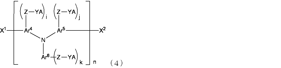
1価の基であるX1、X2としては例えば、ヒドロカルビル基、ヒドロカルビルオキシ基などが挙げられる。
該ヒドロカルビル基がアルキル基である場合、炭素原子数1~20であることが好ましく、メチル基、エチル基、n-プロピル基、iso-プロピル基、n-ブチル基、sec-ブチル基、iso-ブチル基、tert-ブチル基、n-ペンチル基、2,2-ジメチルプロピル基、n-ヘキシル基、シクロヘキシル基、n-ヘプチル基、n-オクチル基、n-ノニル基、n-デシル基、n-ウンデシル基、n-ドデシル基、n-トリデシル基、n-テトラデシル基、n-ペンタデシル基、n-ヘキサデシル基、n-ヘプタデシル基、n-オクタデシル基、n-ノナデシル基、n-イコシル基等の直鎖状、分岐鎖状もしくは環状のアルキル基が例示できる。また、ここに例示するアルキル基において、水素原子の一部が、アルキル基、アルコキシ基、アルキルアミノ基、アリール基、アリールオキシ基、アリールアミノ基、又はハロゲン原子に置換されていてもよく、その場合、当該ヒドロカルビル基の炭素原子数は20以下になるようにする。
また、該ヒドロカルビル基がアリール基である場合は、炭素原子数6~20であることが好ましく、フェニル基、1-ナフチル基、2-ナフチル基、3-フェナントリル基、2-アントリル基等が挙げられる。ここに例示するアリール基において、水素原子の一部が、アルキル基、アルコキシ基、アルキルアミノ基、アリール基又はハロゲン原子に置換されていてもよく、その場合、当該アリール基の炭素原子数は20以下になるようにする。
また、該ヒドロカルビル基がアリール基である場合は、炭素原子数6~20であることが好ましく、フェニル基、1-ナフチル基、2-ナフチル基、3-フェナントリル基、2-アントリル基等が挙げられる。ここに例示するアリール基において、水素原子の一部が、アルキル基、アルコキシ基、アルキルアミノ基、アリール基又はハロゲン原子に置換されていてもよく、その場合、当該アリール基の炭素原子数は20以下になるようにする。
該ヒドロカルビルオキシ基がアルコキシ基である場合、炭素原子数1~20であることが好ましく、メトキシ基、エトキシ基、n-プロピルオキシ基、iso-プロピルオキシ基、n-ブチルオキシ基、sec-ブチルオキシ基、iso-ブチルオキシ基、tert-ブチルオキシ基、n-ペンチルオキシ基、2,2-ジメチルプロピルオキシ基、n-ヘキシルオキシ基、シクロヘキシルオキシ基、n-ヘプチルオキシ基、n-オクチルオキシ基、n-ノニルオキシ基、n-デシルオキシ基、n-ウンデシルオキシ基、n-ドデシルオキシ基、n-トリデシルオキシ基、n-テトラデシルオキシ基、n-ペンタデシルオキシ基、n-ヘキサデシルオキシ基、n-ヘプタデシルオキシ基、n-オクタデシルオキシ基、n-ノナデシルオキシ基、n-イコシルオキシ基等の直鎖状、分岐鎖状もしくは環状のアルコキシ基が例示できる。また、ここに例示するアルコキシ基において、水素原子の一部が、アルキル基、アルコキシ基、アルキルアミノ基、アリール基又はハロゲン原子に置換されていてもよく、その場合、当該アルコキシ基の炭素原子数は20以下になるようにする。
また、該ヒドロカルビルオキシ基がアリールオキシ基である場合は、炭素原子数6~20であることが好ましく、フェニルオキシ基、1-ナフチルオキシ基、2-ナフチルオキシ基、3-フェナントリルオキシ基、2-アントリルオキシ基等が挙げられる。ここに例示するアリールオキシ基において、水素原子の一部が、アルキル基、アルコキシ基、アルキルアミノ基、アリール基、アリールオキシ基、アリールアミノ基、又はハロゲン原子に置換されていてもよく、その場合、当該ヒドロカルビルオキシ基の炭素原子数は20以下になるようにする。
また、該ヒドロカルビルオキシ基がアリールオキシ基である場合は、炭素原子数6~20であることが好ましく、フェニルオキシ基、1-ナフチルオキシ基、2-ナフチルオキシ基、3-フェナントリルオキシ基、2-アントリルオキシ基等が挙げられる。ここに例示するアリールオキシ基において、水素原子の一部が、アルキル基、アルコキシ基、アルキルアミノ基、アリール基、アリールオキシ基、アリールアミノ基、又はハロゲン原子に置換されていてもよく、その場合、当該ヒドロカルビルオキシ基の炭素原子数は20以下になるようにする。
1価の基であるX1、X2としてはさらに下記の基からなる群から選ばれる基が例示される。
-F、-Cl、-Br、-I、-OH、-CN、-CO2H、-CO2R7、-Si(CH3)3、-Si(CH3)2C(CH3)3、-B(OR5)(OR6)、-CO2R7、-COR7、-O-SO2-CH3、-O-SO2-CF3、-O-SO2-(p-C6H4)-CH3、-O-SO2-C6H5、-P(C6H5)2、-P(=O)(C6H5)2、-Ar8
(R5、R6及びR7はそれぞれ独立に1価の基を表し、該1価の基は、フッ素原子、置換基を有していてもよい炭素原子数1~20のアルキル基及び置換基を有していてもよい炭素原子数6~20のアリール基からなる群から選ばれる基で置換されていてもよい。また、R5及びR6は互いに結合して環を形成していてもよい。Ar8は1価の芳香族基を表し、フェニル基、1-ナフチル基、2-ナフチル基、3-フェナントリル基、2-アントリル基等が挙げられる。)
-F、-Cl、-Br、-I、-OH、-CN、-CO2H、-CO2R7、-Si(CH3)3、-Si(CH3)2C(CH3)3、-B(OR5)(OR6)、-CO2R7、-COR7、-O-SO2-CH3、-O-SO2-CF3、-O-SO2-(p-C6H4)-CH3、-O-SO2-C6H5、-P(C6H5)2、-P(=O)(C6H5)2、-Ar8
(R5、R6及びR7はそれぞれ独立に1価の基を表し、該1価の基は、フッ素原子、置換基を有していてもよい炭素原子数1~20のアルキル基及び置換基を有していてもよい炭素原子数6~20のアリール基からなる群から選ばれる基で置換されていてもよい。また、R5及びR6は互いに結合して環を形成していてもよい。Ar8は1価の芳香族基を表し、フェニル基、1-ナフチル基、2-ナフチル基、3-フェナントリル基、2-アントリル基等が挙げられる。)
X1、X2として特に好ましいものは水素原子及び下記の基からなる群から選ばれる基であり、互いに同一であっても異なっていてもよい。
-B(OR5)(OR6)、-Ar8
-B(OR5)(OR6)、-Ar8
nは1以上の整数を表す。nとしては1以上1000000以下が好ましく、1以上500000以下がより好ましく、1以上100000以下がさらに好ましく、1以上1000以下が特に好ましい。
本発明の芳香族化合物のポリスチレン換算の数平均分子量(Mn)は100以上1000000以下であることが好ましく、500以上500000以下であることがより好ましく、1000以上200000以下であることが更に好ましい。ここでのMn値はサイズ排除クロマトグラフィー(SEC)により求まる。
本発明の芳香族化合物のポリスチレン換算の数平均分子量(Mn)は100以上1000000以下であることが好ましく、500以上500000以下であることがより好ましく、1000以上200000以下であることが更に好ましい。ここでのMn値はサイズ排除クロマトグラフィー(SEC)により求まる。
上記式(4)で表される芳香族化合物の具体例としては下記式(2a)~(2c)、(2f)、(2g)及び(2i)~(2z)で表される芳香族化合物が挙げられる。

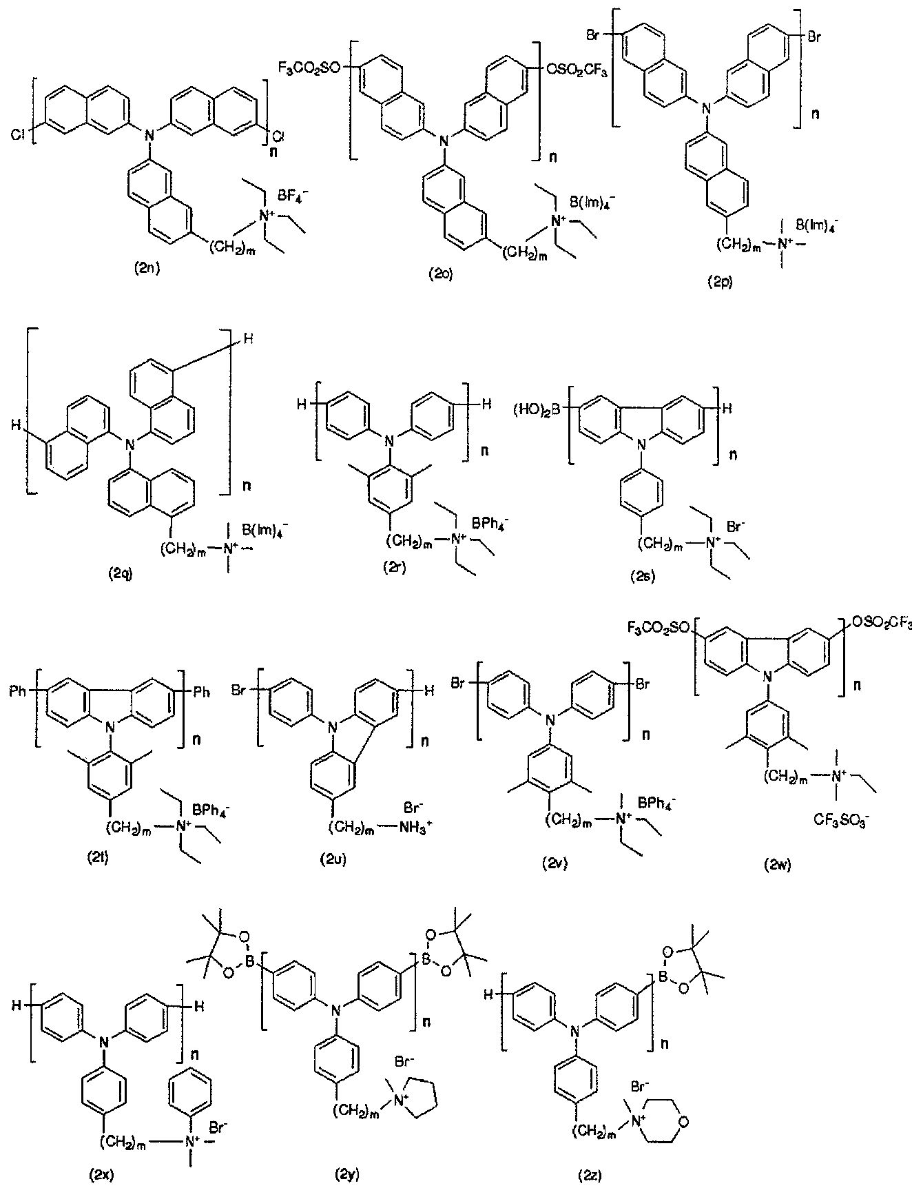
m及びnは前記と同じ意味を表す。
さらに上記式(4)で表される芳香族化合物の具体例としては下記式(2a2)~(2h2)で表される芳香族化合物が挙げられる。

m及びnは前記と同じ意味を表す。
さらに上記式(4)で表される芳香族化合物の具体例としては下記式(2a3)~(2h3)で表される芳香族化合物が挙げられる。
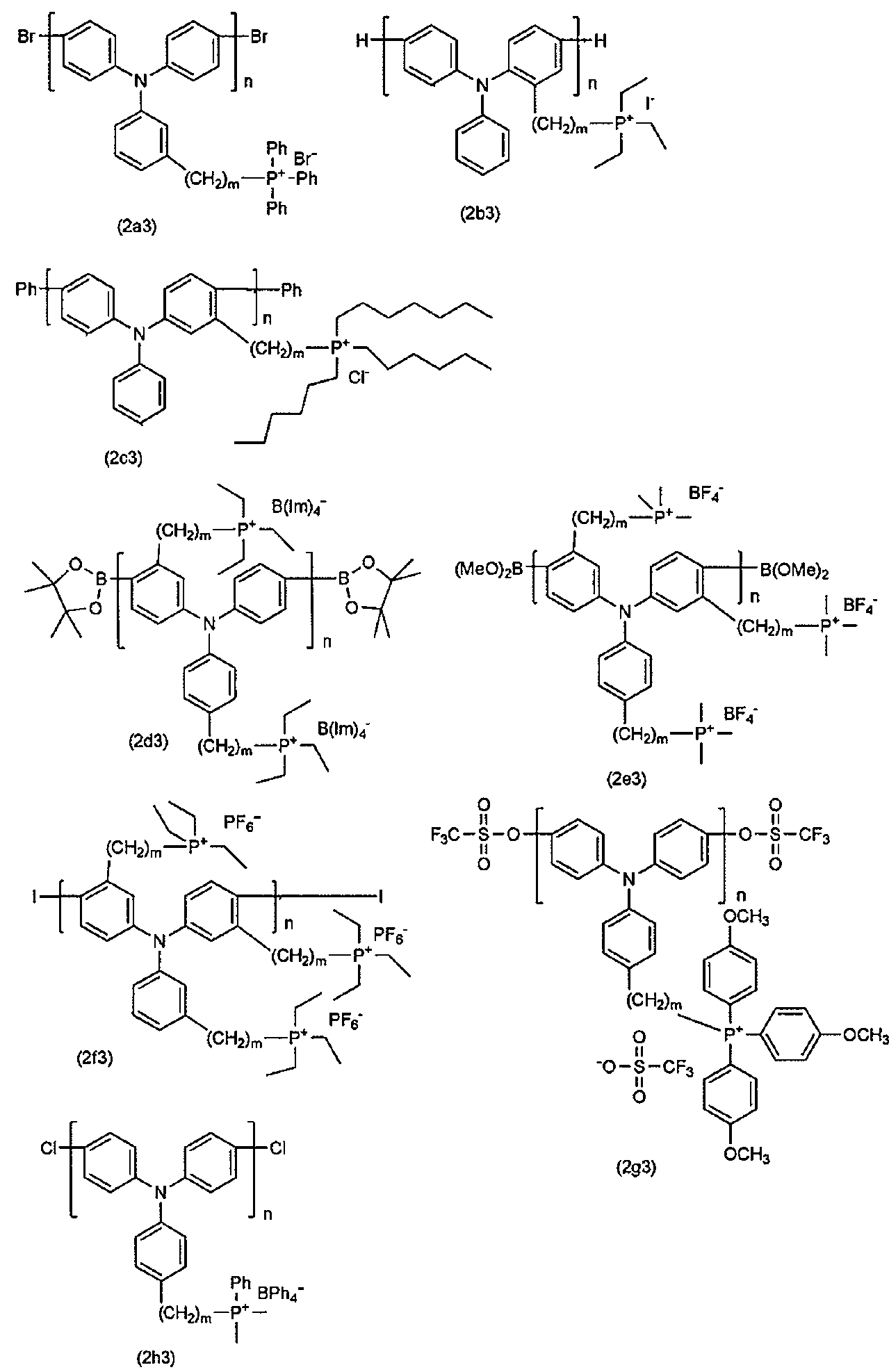
m及びnは前記と同じ意味を表す。
さらに上記式(4)で表される芳香族化合物の具体例としては下記式(2a4)~(2h4)で表される芳香族化合物が挙げられる。
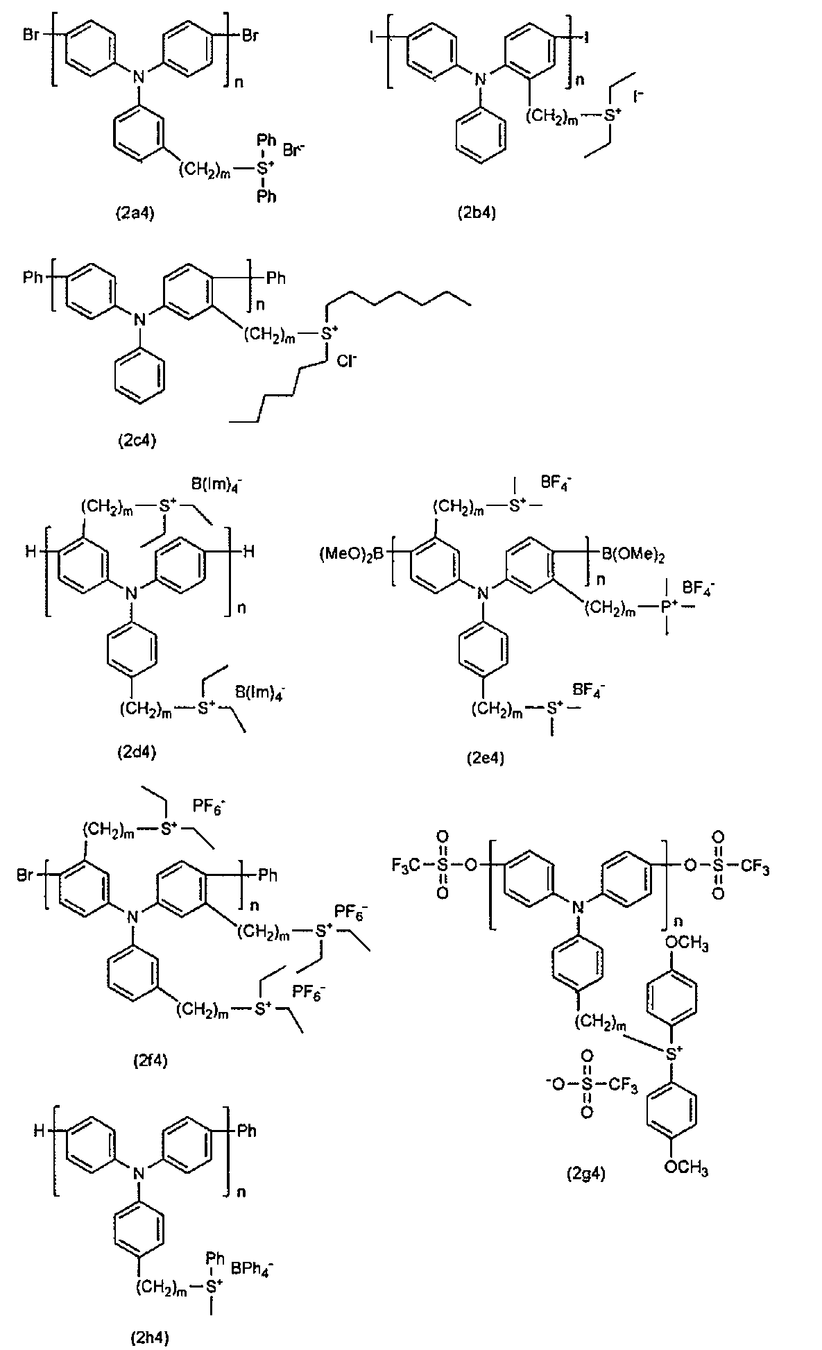
m及びnは前記と同じ意味を表す。
これらの(2a)~(2c)、(2f)、(2g)、(2i)~(2z)、(2a2)~(2h2)、(2a3)~(2h3)及び(2a4)~(2h4)のうち、極性が高くて高極性溶媒にも溶解しやすい点、及び熱による分解が起こりにくい点から、(2a)~(2c)、(2f)、(2g)及び(2i)~(2z)が好ましい。
これらの(2a)~(2c)、(2f)、(2g)及び(2i)~(2z)のうちでも、(2a)、(2b)、(2c)、(2l)、(2k)、(2m)、(2n)、(2p)、(2q)、(2r)、(2s)、(2t)、(2v)、(2y)、(2z)が好ましく、(2a)、(2c)、(2l)、(2p)、(2q)、(2r)、(2t)、(2y)、(2z)がより好ましく、(2a)、(2c)、(2r)、(2t)、(2y)がさらに好ましい。
これらの(2a)~(2c)、(2f)、(2g)及び(2i)~(2z)のうちでも、(2a)、(2b)、(2c)、(2l)、(2k)、(2m)、(2n)、(2p)、(2q)、(2r)、(2s)、(2t)、(2v)、(2y)、(2z)が好ましく、(2a)、(2c)、(2l)、(2p)、(2q)、(2r)、(2t)、(2y)、(2z)がより好ましく、(2a)、(2c)、(2r)、(2t)、(2y)がさらに好ましい。
本発明の一実施形態において、上記式(4)で表される芳香族化合物は、X6及びX7が下記の官能基群から選ばれる官能基であり、互いに同一であっても異なっていてもよく、Ar4、Ar5、Ar6、A、Y、Z、i、j、k及びnが前記と同じ意味を表す、下記式(4-1)で表される芳香族化合物である。
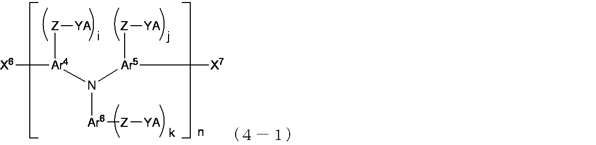
官能基群:-Cl、-Br、-I、-O-SO2-CH3、-O-SO2-CF3、-O-SO2-(p-C6H4)-CH3、-O-SO2-C6H5
上記式(4-1)の具体例としては、上記(2a)、(2c)、(2l)、(2f)、(2g)、(2k)、(2n)、(2o)、(2p)、(2u)、(2v)、(2w)、(2a2)、(2g2)、(2h2)、(2a3)、(2f3)、(2g3),(2h3),(2a4),(2b4),(2g4)が挙げられる。
本発明の別の一実施形態において、上記式(4)で表される芳香族化合物は、X8及びX9が下記の官能基群から選ばれる官能基であり、互いに同一であっても異なっていてもよく、Ar4、Ar5、Ar6、A、Y、Z、i、j、k及びnが前記と同じ意味を表す、下記式(4-2)で表される芳香族化合物である。
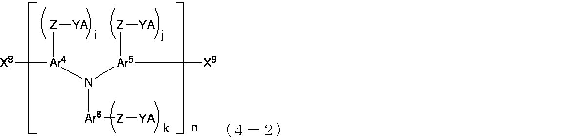
官能基群:-B(OR5)(OR6)(式中、R5及びR6は前記と同じ意味を表す。)
上記式(4-2)の具体例としては、上記(2b)、(2l)、(2y)、(2z)、(2e2),(2f2)、(2d3),(2e3)、(2e4),(2g4)が挙げられる。
さらに本発明は、上記式(4-1)及び/又は上記式(4-2)で表される芳香族化合物を用い、sp2炭素-sp2炭素結合形成反応を行い、上記式(3)で表される構造単位の数及び/又は上記式(4)中の前記nを増加せしめる製造方法を提供する。以下、好適な方法に関し説明する。
かかる製造方法としては、ゼロ価遷移金属錯体を触媒とするカップリング反応を単位反応とする重合が好適であり、ゼロ価遷移金属錯体と、当該ゼロ価遷移金属錯体の中心金属と配位できる二座以上の化合物(以下、「配位子化合物」ということがある)の存在下での重合がより好適である。
かかる製造方法としては、ゼロ価遷移金属錯体を触媒とするカップリング反応を単位反応とする重合が好適であり、ゼロ価遷移金属錯体と、当該ゼロ価遷移金属錯体の中心金属と配位できる二座以上の化合物(以下、「配位子化合物」ということがある)の存在下での重合がより好適である。
上記式(4-1)で表される芳香族化合物のみを用い、sp2炭素-sp2炭素結合形成反応を行う場合には、ゼロ価遷移金属錯体として、ニッケル(0)錯体を用いることが好ましい。
また上記式(4-1)で表される芳香族化合物とともに下記式(13)で表される芳香族化合物を用い、sp2炭素-sp2炭素結合形成反応を行う場合にも、ゼロ価遷移金属錯体として、ニッケル(0)錯体を用いることが好ましい。

ニッケル(0)錯体としては、例えば、ニッケル(0)ビス(シクロオクタジエン)、ニッケル(0)(エチレン)ビス(トリフェニルホスフィン)、ニッケル(0)テトラキス(トリフェニルホスフィン)等のゼロ価ニッケル錯体(ニッケル(0)錯体)でもよく、ハロゲン化ニッケル(例えば、フッ化ニッケル、塩化ニッケル、臭化ニッケル、ヨウ化ニッケル等)、ニッケルカルボン酸塩(例えば、ギ酸ニッケル、酢酸ニッケル等)、硫酸ニッケル、炭酸ニッケル、硝酸ニッケル、ニッケルアセチルアセトナート、(ジメトキシエタン)塩化ニッケル等の2価ニッケル化合物を反応系中で還元、錯体化してニッケル(0)錯体にしたものでもよい。これらの中でも、ニッケル(0)ビス(シクロオクタジエン)を使用するか、ハロゲン化ニッケルを反応系中でニッケル(0)錯体にしたものが、本発明の芳香族化合物を得るうえで好適である。
前記ゼロ価遷移金属錯体の使用量は、使用する芳香族化合物の種類及び得られるカップリング生成物の分子量により適宜最適化できる。脱離基(-X6、-X7)1モルに対して、ゼロ価遷移金属錯体0.4~5モルの使用量が好適である。
ゼロ価遷移金属錯体に加え、配位子化合物を共存させることは、反応中のゼロ価遷移金属錯体自身の安定性が良好になり、反応が円滑に進行するうえで特に好適である。ニッケル(0)錯体を触媒として使用する場合において、配位子化合物としては、2,2'-ビピリジン、1,10-フェナントロリン、メチレンビスオキサゾリン、N,N'-テトラメチルエチレンジアミンが好ましく、2,2'-ビピリジンが特に好ましい。このような配位子化合物を使用する場合、その使用量は、ゼロ価遷移金属錯体の中心金属(ニッケルなど)1モルに対して、通常0.2~2モルの範囲であり、好ましくは1~1.5モルの範囲である。
ゼロ価遷移金属錯体がニッケル(0)錯体の場合、ニッケル(0)錯体としては、2価ニッケル化合物を用い重合の反応系中でニッケル(0)錯体にしたものを用いることもできる。この場合、ニッケルを還元し得る還元剤が必要となる。該還元剤としては亜鉛が好ましく使用され、この亜鉛は通常粉末状のものが用いられる。亜鉛を使用する場合、その使用量は、使用するモノマー1モルに対して、通常等モル以上10モル倍以下、好ましくは等モル以上5モル倍以下から選択される。亜鉛の使用量の上限は、反応後の後処理が煩雑にならないように、また経済的にも不利にならないようにして選択される。なお、2価ニッケル化合物と亜鉛とを併用するのは、該2価ニッケル化合物の使用当量が、使用するモノマーの使用当量に対して下回る場合に特に有利である。
反応は、通常溶媒の存在下に実施される。溶媒としては、使用するモノマー及び生成する本発明の芳香族化合物が溶解し得る溶媒であればよい。かかる溶媒の具体例としては、トルエン、キシレン等の芳香族炭化水素溶媒;テトラヒドロフラン、1,4-ジオキサン等のエーテル溶媒;ジメチルスルホキシド(DMSO)、N-メチル-2-ピロリドン(NMP)、N,N-ジメチルホルムアミド(DMF)、N,N-ジメチルアセトアミド(DMAc)、ヘキサメチルホスホリックトリアミド等の非プロトン性極性溶媒;ジクロロメタン、ジクロロエタン等のハロゲン化炭化水素溶媒等が挙げられる。かかる溶媒は、単独で用いてもよいし、2種以上を混合して用いてもよい。なかでも、エーテル溶媒及び非プロトン性極性溶媒が好ましく、テトラヒドロフラン、ジメチルスルホキシド、N-メチル-2-ピロリドン、N,N-ジメチルアセトアミド又はこれらから選ばれる2種以上の混合溶媒がより好ましい。溶媒の使用量は、多すぎると反応が進行し難くなる傾向にあり、少なすぎると反応液が著しく高粘度化して後処理が煩雑になるという場合があるため、反応せしめる芳香族化合物の合計重量に対して、通常1~200重量倍、好ましくは5~100重量倍とするのがよい。
反応は、通常、窒素ガス等の不活性ガスの雰囲気下で実施される。
また反応温度は、通常0~250℃であり、好ましくは30~100℃である。
反応時間は、通常0.5~48時間から選ばれるが、例えば、反応途中の反応溶液を所定時間おきにサンプリングし、生成物の分子量測定等の分析を行って、所望の生成物が得られるようにして、反応時間を決定することが好ましい。
また反応温度は、通常0~250℃であり、好ましくは30~100℃である。
反応時間は、通常0.5~48時間から選ばれるが、例えば、反応途中の反応溶液を所定時間おきにサンプリングし、生成物の分子量測定等の分析を行って、所望の生成物が得られるようにして、反応時間を決定することが好ましい。
反応後の反応溶液から、生成物を取り出すには各種公知の手段を用いればよい。典型的には、生成物を溶解し難い貧溶媒を、反応溶液と混合してポリマーを析出させ、析出した生成物を濾過等により分離するといった手段を用いればよく、かかる手段は操作が簡便であるという利点がある。なお、かかる貧溶媒としては例えば、水、メタノール、エタノール、アセトニトリル等が挙げられ、水及びメタノールが好ましい。得られたポリマーの分子量や化学構造は、ゲル浸透クロマトグラフィ、高速液体クロマトグラフィ、核磁気共鳴スペクトル(NMR)等の通常の分析手段により求めることができる。
ボロン官能基を有する芳香族化合物を用いてsp2炭素-sp2炭素結合形成反応を行う場合は、塩基存在下、ゼロ価遷移金属錯体としてパラジウムを用いる、Suzukiカップリングを利用する。
上記式(4-1)で表される芳香族化合物と上記式(4-2)で表される芳香族化合物を用いる場合、上記式(4-1)で表される芳香族化合物と下記式(14)で表される芳香族化合物を用いる場合、上記式(4-1)で表される芳香族化合物、上記式(4-2)で表される芳香族化合物、及び下記式(14)で表される芳香族化合物を用いる場合、などが例として挙げられる。
上記式(4-1)で表される芳香族化合物と上記式(4-2)で表される芳香族化合物を用いる場合、上記式(4-1)で表される芳香族化合物と下記式(14)で表される芳香族化合物を用いる場合、上記式(4-1)で表される芳香族化合物、上記式(4-2)で表される芳香族化合物、及び下記式(14)で表される芳香族化合物を用いる場合、などが例として挙げられる。

上記カップリング反応における反応性を有する基のうち、約50モルパーセントはボロン官能基より選ばれることが好ましい。
本発明において用いるに適した有機溶媒は、モノマーを少なくとも1パーセント、より好ましくは少なくとも2パーセントの溶液濃度に溶解することのできるものを含む。好ましくは、この溶媒はC6-C20(即ち、炭素原子数6~20)の芳香族基含有化合物であり、より好ましくはベンゼン、トルエン、キシレン、エチルベンゼン、メシチレン、アニソール、又はこれらのフッ素化体である。これらのうち、トルエンが特に好ましい。反応中の溶媒の体積は、反応混合物はポリマーである芳香族化合物の分子量の増大により粘度が増加するために、還流において有効に混合できるようでなければならない。これは通常、芳香族化合物1gに対して5~20mLであり、好ましくは芳香族化合物1gに対してトルエン約10mLである。
本発明において有効な塩基の例は、アルカリ金属カーボネート及びバイカーボネートを含む。好ましくは、この塩基は水性アルカリ金属カーボネートの溶液、例えば1mol/L~2mol/Lの炭酸ナトリウムもしくはカリウムである。
Pd(II)塩又はPd(0)錯体としてパラジウムを加えてもよい。酢酸Pdが好ましいPd(II)塩であり、Pd(Ph3P)4が好ましいPd(0)錯体である。Pd(II)塩を用いる場合、反応混合物に、Pd塩1モルに対して2~4モル当量のトリフェニルホスフィン(Ph3P)を加えることが有利である。または、Pd(II)-Ph3P錯体、例えばPdCl2(Ph3P)2を用いる。ボロン官能基に対するPdの量は、好ましくはボロン官能基2モルに対して1×10⁻⁶モル~1モル、より好ましくは1×10⁻⁵モル~1×10⁻¹モル、特に好ましくは1×10⁻⁴モル~1×10⁻³モルである。
反応温度の好ましい上限は、水性塩基及び有機溶媒中のモノマーの溶液からなる不混和性液体混合物の沸点である。通常、反応温度を好ましくは150℃以下、より好ましくは130℃以下、特に好ましくは120℃以下に制限する。
反応は、通常、窒素ガス等の不活性ガスの雰囲気下で実施される。
反応時間は、通常0.5~48時間から選ばれるが、例えば、反応途中の反応溶液を所定時間おきにサンプリングし、生成物の分子量測定等の分析を行って、所望の生成物が得られるようにして、反応時間を決定することが好ましい。
反応時間は、通常0.5~48時間から選ばれるが、例えば、反応途中の反応溶液を所定時間おきにサンプリングし、生成物の分子量測定等の分析を行って、所望の生成物が得られるようにして、反応時間を決定することが好ましい。
反応後の反応溶液から、生成物を取り出すには各種公知の手段を用いればよい。典型的には、生成物を溶解し難い貧溶媒を、反応溶液と混合してポリマー(芳香族化合物)を析出させ、析出した生成物を濾過等により分離するといった手段を用いればよく、かかる手段は操作が簡便であるという利点がある。なお、かかる貧溶媒としては例えば、水、メタノール、エタノール、アセトニトリル等が挙げられ、水及びメタノールが好ましい。得られたポリマーの分子量や化学構造は、ゲル浸透クロマトグラフィ、高速液体クロマトグラフィ、核磁気共鳴スペクトル(NMR)等の通常の分析手段により求めることができる。
本発明は下記式(7)で表される構造単位を有する芳香族化合物、即ち、脱離基を炭化水素側鎖に有する芳香族化合物を提供する。
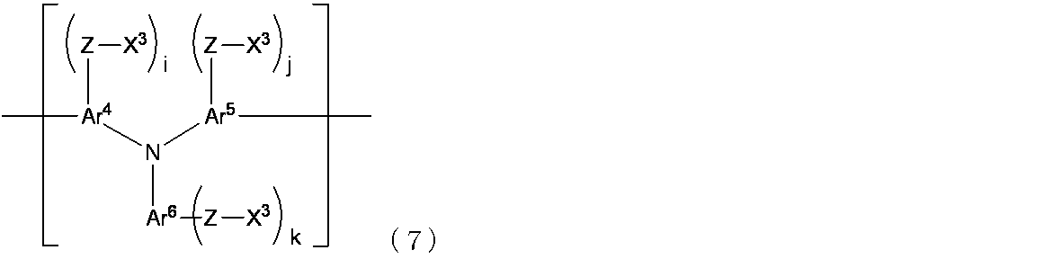
脱離基であるX3の例としては、下記の官能基群から選ばれる基が挙げられる。X3が2種類以上ある場合、それらは互いに同一であっても異なっていてもよい。
-Cl、-Br、-I、-O-SO2-CH3、-O-SO2-CF3、-O-SO2-
(p-C6H4)-CH3、-O-SO2-C6H5
-Cl、-Br、-I、-O-SO2-CH3、-O-SO2-CF3、-O-SO2-
(p-C6H4)-CH3、-O-SO2-C6H5
上記式(7)で表される構造単位の例としては下記(3a)~(3w)が挙げられる。


mは前記と同じ意味を表す。
さらに上記式(7)で表される構造単位の具体例としては下記(3a2)~(3h2)が挙げられる。mは前記と同じ意味を表す。
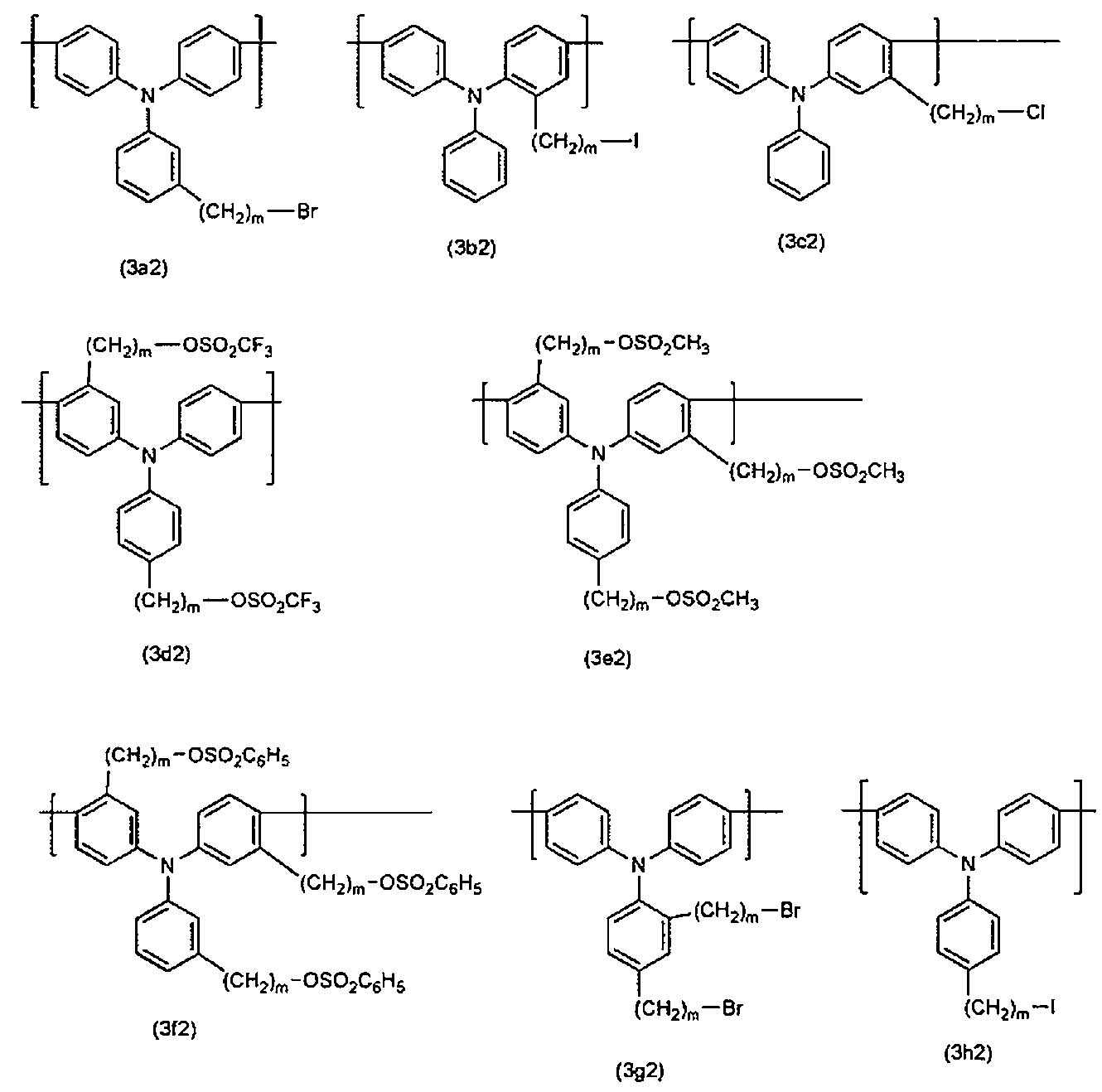
これらのうち、(3a)、(3b)、(3c)、(3d)、(3e)、(3f)、(3g)、(3i)、(3j)、(3l)、(3n)、(3o)、(3p)、(3q)、(3r)、(3s)、(3v)、(3w)が好ましく、(3a)、(3c)、(3d)、(3i)、(3l)、(3n)、(3p)、(3q)、(3r)、(3s)、(3v)、(3w)がより好ましく、(3a)、(3c)、(3d)、(3i)、(3l)、(3n)、(3r)、(3s)、(3v)がさらに好ましく、(3a)、(3c)、(3d)、(3i)、(3r)、(3s)がより一層好ましい。
本発明の、前記式(7)で表される構造単位を有する、芳香族化合物における構造単位の合計を100モル%としたとき、前記式(7)で表される構造単位の割合が1モル%以上100モル%以下の範囲であることが好ましく、1モル%以上99モル%以下の範囲であることがより好ましく、5モル%以上90モル%以下の範囲であることがさらに好ましく、10モル%以上80モル%以下の範囲であることが一層好ましく、20モル%以上70モル%以下の範囲であることが特に好ましい。
また本発明は下記式(8)で表される芳香族化合物、即ち、脱離基を炭化水素側鎖に有する芳香族化合物を提供する。
上記式(8)の例としては下記式(4a)~(4z)が挙げられる。
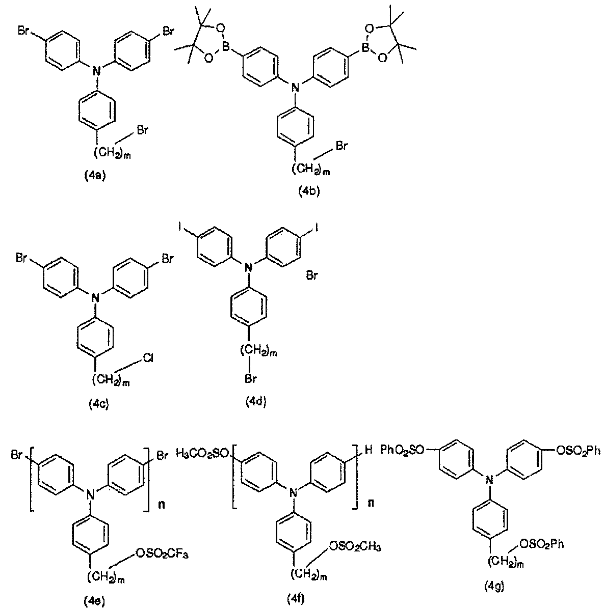

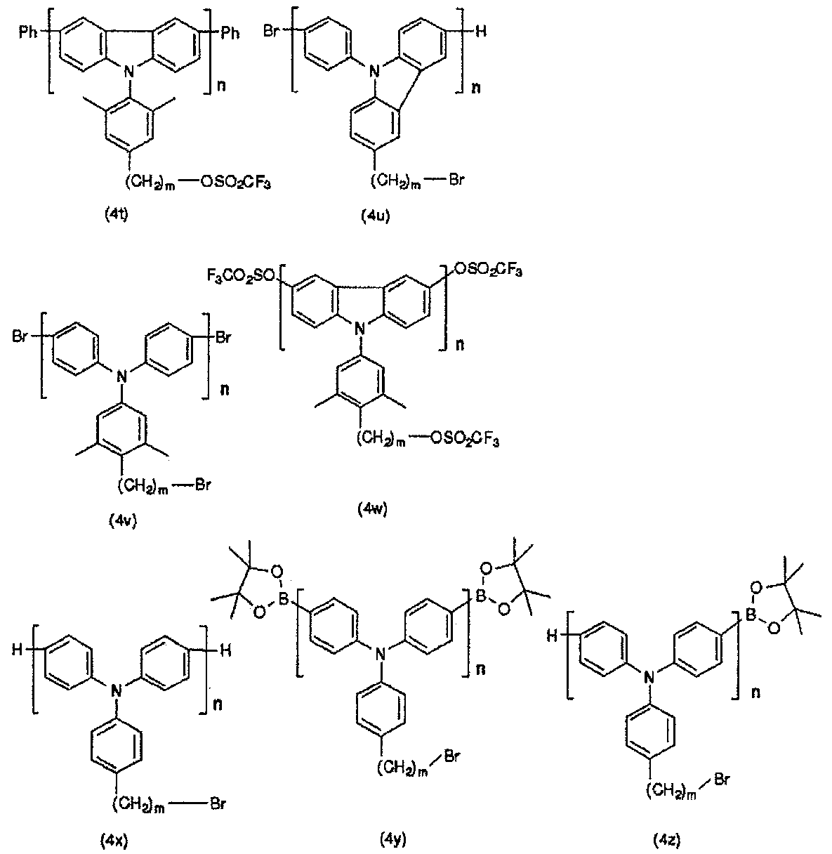
m及びnは前記と同じ意味を表す。
さらに上記式(8)の例としては下記式(4a2)~(4h2)が挙げられる。m及びnは前記と同じ意味を表す。
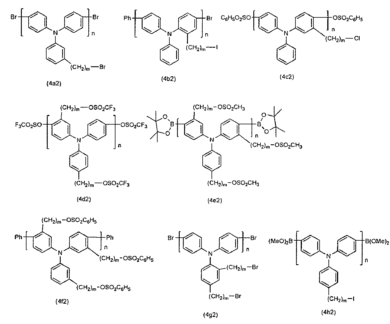
これらのうち、(4a)、(4b)、(4c)、(4d)、(4e)、(4f)、(4g)、(4i)、(4j)、(4l)、(4n)、(4o)、(4p)、(4q)、(4r)、(4s)、(4v)、(4w)、(4y)、(4z)が好ましく、(4a)、(4c)、(4d)、(4i)、(4l)、(4n)、(4p)、(4q)、(4r)、(4s)、(4v)、(4w)がより好ましく、(4a)、(4c)、(4d)、(4i)、(4l)、(4n)、(4r)、(4s)、(4v)がさらに好ましく、(4a)、(4c)、(4d)、(4i)、(4r)、(4s)がより一層好ましい。
本発明の一実施形態において、上記式(8)で表される芳香族化合物は、X6及びX7が前記と同様に下記の官能基群から選ばれる官能基であり、互いに同一であっても異なっていてもよく、Ar4、Ar5、Ar6、Z、X3、i、j、k及びnが前記と同じ意味を表す、下記式(8-1)で表される芳香族化合物を提供する。
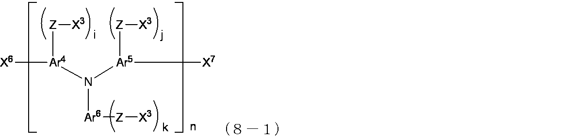
官能基群:-Cl、-Br、-I、-O-SO2-CH3、-O-SO2-CF3、-O-SO2-(p-C6H4)-CH3、-O-SO2-C6H5
上記式(8-1)の具体例としては、上記(4a)、(4c)、(4d)、(4e)、(4f)、(4g)、(4h)、(4k)、(4n)、(4o)、(4p)、(4v)、(4w)、(4a2)、(4c2)、(4d2)、(4g2)が挙げられる。
本発明の別の一実施形態において、上記式(8)で表される芳香族化合物は、X8、X9が前記と同様に下記の官能基群から選ばれる官能基であり、互いに同一であっても異なっていてもよく、Ar4、Ar5、Ar6、Z、X3、i、j、k及びnが前記と同じ意味を表す、下記式(8-2)で表される芳香族化合物を提供する。

官能基群:-B(OR5)(OR6)(式中、R5及びR6は前記と同じ意味を表す。)
上記式(8-2)の具体例としては、上記(4b)、(4h)、(4l)、(4y)、(4e2)、(4h2)が挙げられる。
本発明はまた、上記式(8)で表される化合物を用い、sp2炭素-sp2炭素結合形
成反応を行い、上記式(7)で表される構造単位の数及び/又は上記式(8)で表される芳香族化合物の上記nを増加させる、製造方法を提供する。この場合、先述の式(3)で表される構造単位を有する芳香族化合物及び/又は式(4)で表される芳香族化合物の製造方法を同様に適用できる。
成反応を行い、上記式(7)で表される構造単位の数及び/又は上記式(8)で表される芳香族化合物の上記nを増加させる、製造方法を提供する。この場合、先述の式(3)で表される構造単位を有する芳香族化合物及び/又は式(4)で表される芳香族化合物の製造方法を同様に適用できる。
特開2009-242724号公報記載の方法などの公知の方法で、上記式(8-1)又は(8-2)中のX3を、所望のアニオンAを有するYAに交換することができる。
更に本発明は、上記式(7)で表される構造単位を有する芳香族化合物を、下記式(11-1)で表される窒素化合物、下記式(11-2)で表されるリン化合物、下記式(11-3)で表される硫黄化合物又はそれら化合物の2種以上の組み合わせと反応させることにより、該芳香族化合物をそのオニウム塩に変換することを含む、上記式(3)で表される構造単位を有する芳香族化合物の製造方法を提供する。
NR1R2R3 (11-1)
PR1R2R3 (11-2)
SR1R2 (11-3)
(式(11-1)、(11-2)及び(11-3)の各々において、R1、R2及びR3は前記のとおりである。)
NR1R2R3 (11-1)
PR1R2R3 (11-2)
SR1R2 (11-3)
(式(11-1)、(11-2)及び(11-3)の各々において、R1、R2及びR3は前記のとおりである。)
式(11-1)で表される窒素化合物としては、第3級アミン化合物が好ましく用いられる。該窒素化合物の具体例としては、トリメチルアミン、トリエチルアミン、トリ-1-プロピルアミン、トリ-2-プロピルアミン、トリ-n-ブチルアミン、トリ-2-ブチルアミン、トリ-1-ペンチルアミン、トリ-2-ペンチルアミン、トリ-3-ペンチルアミン、トリネオペンチルアミン、トリシクロペンチルアミン、トリ-1-ヘキシルアミン、トリ-2-ヘキシルアミン、トリ-3-ヘキシルアミン、ピリジン、N-メチルイミダゾール、N-メチルピロリジン、N-メチルモルホリン等が挙げられる。
式(11-2)で表されるリン化合物としては、第3級ホスフィン化合物が好ましく用いられる。該ホスフィン化合物の具体例としては、トリメチルホスフィン、トリエチルホスフィン、トリ-1-プロピルホスフィン、トリ-2-プロピルホスフィン、トリ-n-ブチルホスフィン、トリ-2-ブチルホスフィン、トリ-1-ペンチルホスフィン、トリ-2-ペンチルホスフィン、トリ-3-ペンチルホスフィン、トリネオペンチルホスフィン、トリシクロペンチルホスフィン、トリ-1-ヘキシルホスフィン、トリ-2-ヘキシルホスフィン、トリ-3-ヘキシルホスフィン、トリフェニルホスフィン、トリ(4-メチルフェニル)ホスフィン、トリ(3-メチルフェニル)ホスフィン、トリ(2-メチルフェニル)ホスフィン、トリ(4-メトキシフェニル)ホスフィン、トリ(3-メトキシフェニル)ホスフィン、トリ(2-メトキシフェニル)ホスフィン等が挙げられる。
式(11-3)で表される硫黄化合物としては、スルフィド化合物が好ましく用いられる。該スルフィド化合物の具体例としては、ジメチルスルフィド、ジエチルスルフィド、ジ-1-プロピルスルフィド、ジ-2-プロピルスルフィド、ジ-n-ブチルスルフィド、ジ-2-ブチルスルフィド、ジ-1-ペンチルスルフィド、ジ-2-ペンチルスルフィド、ジ-3-ペンチルスルフィド、ジネオペンチルスルフィド、ジシクロペンチルスルフィド、ジ-1-ヘキシルスルフィド、ジ-2-ヘキシルスルフィド、ジ-3-ヘキシルスルフィド、ジフェニルスルフィド、ジ(4-メチルフェニル)スルフィド、ジ(3-メチルフェニル)スルフィド、ジ(2-メチルフェニル)スルフィド、ジ(4-メトキシフェニル)スルフィド、ジ(3-メトキシフェニル)スルフィド、ジ(2-メトキシフェニル)スルフィド等が挙げられる。
これらの式(11-1)、(11-2)及び(11-3)で表される化合物のうち、得られる芳香族化合物が高い極性を有し高極性溶媒にも溶解しやすい点、及び該芳香族化合物の熱による分解が起こりにくい点から、式(11-1)の窒素化合物を用いることが好ましい。
本発明は上記式(7)で表される芳香族化合物が上記式(8)で表される芳香族化合物であり、上記式(3)で表される芳香族化合物が上記式(4)で表される芳香族化合物である、上記製造方法を提供する。
本発明の製造方法においては、上記式(7)で表される芳香族化合物中のX3で表される脱離基に、前記窒素化合物、前記リン化合物、前記硫黄化合物又はそれら化合物の2種以上の組み合わせを反応させることが好ましい。
本発明は、下記式(5)で表される構造単位を有する芳香族化合物を提供する。

Ar1、Ar2及びAr3は、それぞれ独立に、置換基を有していてもよい、2価の芳香族基を表し、Ar1、Ar2及びAr3の少なくとも2個は互いに結合して環を形成していてもよい。該2価の芳香族基としては、1,3-フェニレン基、1,4-フェニレン基等の2価の単環性芳香族基;ナフタレン-1,3-ジイル基、ナフタレン-1,4-ジイル基、ナフタレン-1,5-ジイル基、ナフタレン-1,6-ジイル基、ナフタレン-1,7-ジイル基、ナフタレン-2,6-ジイル基、ナフタレン-2,7-ジイル基等の2価の縮合環系芳香族基;ピリジン-2,5-ジイル基、ピリジン-2,6-ジイル基、キノキサリン-2,6-ジイル基、チオフェン-2,5-ジイル基等の2価のヘテロ芳香族基等を挙げることができる。これらのなかでも、2価の単環性芳香族基及び2価の縮合環系芳香族基が好ましく、1,3-フェニレン基、1,4-フェニレン基、ナフタレン-1,4-ジイル基、ナフタレン-1,5-ジイル基、ナフタレン-2,6-ジイル基及びナフタレン-2,7-ジイル基からなる群から選ばれるものがより好ましく、1,3-フェニレン基又は1,4-フェニレン基がさらに好ましく、1,4-フェニレン基が特に好ましい。
本発明の、前記式(5)で表される構造単位を有する、芳香族化合物における構造単位の合計を100モル%としたとき、前記式(5)で表される構造単位の割合が1モル%以上100モル%以下の範囲であることが好ましく、1モル%以上99モル%以下の範囲であることがより好ましく、5モル%以上90モル%以下の範囲であることがさらに好ましく、10モル%以上80モル%以下の範囲であることが一層好ましく、20モル%以上70モル%以下の範囲であることが特に好ましい。
上記式(5)の具体例として、上記で例示した構造単位(1a)~(1c)、(1f)、(1g)及び(1i)~(1z)が挙げられる。
これらのうち、(1a)、(1b)、(1c)、(1l)、(1k)、(1m)、(1n)、(1p)、(1q)、(1r)、(1s)、(1t)、(1v)、(1y)、(1z)が好ましく、(1a)、(1c)、(1l)、(1p)、(1q)、(1r)、(1t)、(1y)、(1z)がより好ましく、(1a)、(1c)、(1r)、(1t)、(1y)がさらに好ましい。
これらのうち、(1a)、(1b)、(1c)、(1l)、(1k)、(1m)、(1n)、(1p)、(1q)、(1r)、(1s)、(1t)、(1v)、(1y)、(1z)が好ましく、(1a)、(1c)、(1l)、(1p)、(1q)、(1r)、(1t)、(1y)、(1z)がより好ましく、(1a)、(1c)、(1r)、(1t)、(1y)がさらに好ましい。
また、本発明の芳香族化合物には、繰り返し単位として上記式(5)で表される構造単位の他に、上記式(12)で表される構造単位を含んでいてもよい。式(12)で表される構造単位の具体例は上記のとおりである。このような構造単位を含むことにより、本発明の芳香族化合物の有する正孔注入性がさらに向上しうる。式(12)で表される構造単位の好ましい例及びより好ましい例も上記のとおりである。
本発明はまた、下記式(6)で表される芳香族化合物を提供する。

上記式(6)で表される芳香族化合物の具体例としては、上記式(2a)~(2c)、(2f)、(2g)及び(2i)~(2z)で表される芳香族化合物が挙げられる。
これらのうち、(2f)、(2i)、(2j)、(2m)、(2q)、(2r)、(2s)、(2t)、(2u)、(2x)、(2z)が好ましく、(2i)、(2j)、(2m)、(2q)、(2r)、(2t)、(2x)がより好ましい。
本発明の一実施形態において、上記式(6)で表される芳香族化合物は、X6及びX7が下記の官能基群から選ばれる官能基であり、互いに同一であっても異なっていてもよく、Ar1、Ar2、Ar3、A、Z、R1、R2、R3及びnが前記と同じ意味を表す、下記式(6-1)で表される芳香族化合物である。
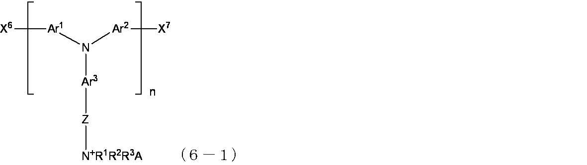
官能基群:-Cl、-Br、-I、-O-SO2-CH3、-O-SO2-CF3、-O-SO2-(p-C6H4)-CH3、-O-SO2-C6H5
上記式(6-1)の具体例としては、上記(2a)、(2c)、(2l)、(2f)、(2g)、(2k)、(2n)、(2o)、(2p)、(2u)、(2v)、(2w)が挙げられる。
本発明の別の一実施形態において、上記式(6)で表される芳香族化合物は、X8及びX9が下記の官能基群から選ばれる官能基であり、互いに同一であっても異なっていてもよく、Ar1、Ar2、Ar3、A、Z、R1、R2、R3及びnが前記と同じ意味を表す、下記式(6-2)で表される芳香族化合物である。
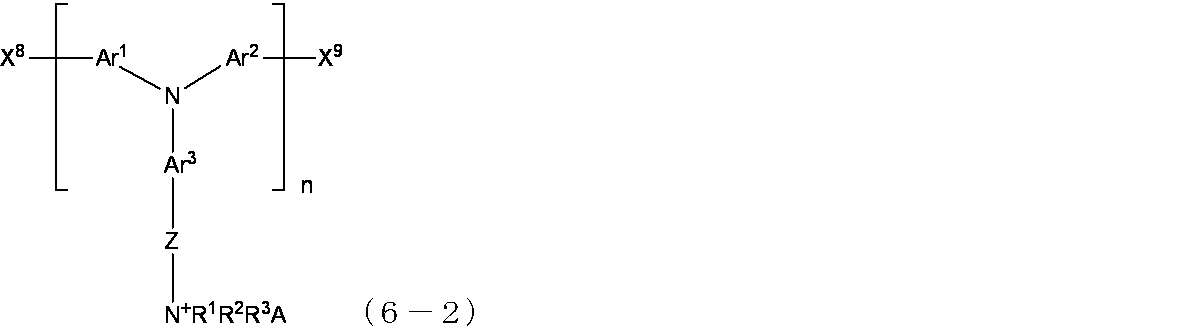
官能基群:-B(OR5)(OR6)(式中、R5及びR6は前記と同じ意味を表す。)
上記式(6-2)の具体例としては、上記(2b)、(2l)、(2y)、(2z)が挙げられる。
さらに本発明は、上記式(6-1)及び/又は上記式(6-2)で表される芳香族化合物を用い、sp2炭素-sp2炭素結合形成反応を行い、上記式(5)で表される構造単位の数及び/又は上記式(6)中の前記nを増加せしめる製造方法を提供する。この場合、先述の式(4-1)及び/又は(4-2)で表される芳香族化合物を用いて先述の式(3)で表される構造単位を有する芳香族化合物及び/又は式(4)で表される芳香族化合物を製造する方法と同様の方法を用いることができる。
本発明は下記式(9)で表される構造単位を有する、芳香族化合物を提供する。

上記式(9)で表される構造単位の例としては、上記で例示した構造単位(3a)~(3w)が挙げられる。
これらのうち、(3a)、(3b)、(3c)、(3d)、(3e)、(3f)、(3g)、(3i)、(3j)、(3l)、(3n)、(3o)、(3p)、(3q)、(3r)、(3s)、(3v)、(3w)が好ましく、(3a)、(3c)、(3d)、(3i)、(3l)、(3n)、(3p)、(3q)、(3r)、(3s)、(3v)、(3w)がより好ましく、(3a)、(3c)、(3d)、(3i)、(3l)、(3n)、(3r)、(3s)、(3v)がさらに好ましく、(3a)、(3c)、(3d)、(3i)、(3r)、(3s)がより一層好ましい。
これらのうち、(3a)、(3b)、(3c)、(3d)、(3e)、(3f)、(3g)、(3i)、(3j)、(3l)、(3n)、(3o)、(3p)、(3q)、(3r)、(3s)、(3v)、(3w)が好ましく、(3a)、(3c)、(3d)、(3i)、(3l)、(3n)、(3p)、(3q)、(3r)、(3s)、(3v)、(3w)がより好ましく、(3a)、(3c)、(3d)、(3i)、(3l)、(3n)、(3r)、(3s)、(3v)がさらに好ましく、(3a)、(3c)、(3d)、(3i)、(3r)、(3s)がより一層好ましい。
本発明の、前記式(9)で表される構造単位を有する、芳香族化合物における構造単位の合計を100モル%としたとき、前記式(9)で表される構造単位の割合が1モル%以上100モル%以下の範囲であることが好ましく、1モル%以上99モル%以下の範囲であることがより好ましく、5モル%以上90モル%以下の範囲であることがさらに好ましく、10モル%以上80モル%以下の範囲であることが一層好ましく、20モル%以上70モル%以下の範囲であることが特に好ましい。
本発明はまた、下記式(10)で表される、芳香族化合物を提供する。

上記式(10)の例としては上記式(4a)~(4z)が挙げられる。
これらのうち、(4a)、(4b)、(4c)、(4d)、(4e)、(4f)、(4g)、(4i)、(4j)、(4l)、(4n)、(4o)、(4p)、(4q)、(4r)、(4s)、(4v)、(4w)、(4y)、(4z)が好ましく、(4a)、(4c)、(4d)、(4i)、(4l)、(4n)、(4p)、(4q)、(4r)、(4s)、(4v)、(4w)がより好ましく、(4a)、(4c)、(4d)、(4i)、(4l)、(4n)、(4r)、(4s)、(4v)がさらに好ましく、(4a)、(4c)、(4d)、(4i)、(4r)、(4s)がより一層好ましい。
これらのうち、(4a)、(4b)、(4c)、(4d)、(4e)、(4f)、(4g)、(4i)、(4j)、(4l)、(4n)、(4o)、(4p)、(4q)、(4r)、(4s)、(4v)、(4w)、(4y)、(4z)が好ましく、(4a)、(4c)、(4d)、(4i)、(4l)、(4n)、(4p)、(4q)、(4r)、(4s)、(4v)、(4w)がより好ましく、(4a)、(4c)、(4d)、(4i)、(4l)、(4n)、(4r)、(4s)、(4v)がさらに好ましく、(4a)、(4c)、(4d)、(4i)、(4r)、(4s)がより一層好ましい。
本発明の一実施形態において、上記式(10)で表される芳香族化合物は、X6及びX7が前記と同様に下記の官能基群から選ばれる官能基であり、互いに同一であっても異なっていてもよく、Ar1、Ar2、Ar3、Z、X3及びnが前記と同じ意味を表す、下記式(10-1)で表される芳香族化合物を提供する。

官能基群:-Cl、-Br、-I、-O-SO2-CH3、-O-SO2-CF3、-O-SO2-(p-C6H4)-CH3、-O-SO2-C6H5
上記式(10-1)の具体例としては、上記(4a)、(4c)、(4d)、(4e)、(4g)、(4h)、(4k)、(4n)、(4o)、(4p)、(4v)、(4w)が挙げられる。
本発明の別の一実施形態において、上記式(10)で表される芳香族化合物は、X8及びX9が前記と同様に下記の官能基群から選ばれる官能基であり、互いに同一であっても異なっていてもよく、Ar1、Ar2、Ar3、Z、X3及びnが前記と同じ意味を表す、下記式(10-2)で表される芳香族化合物を提供する。
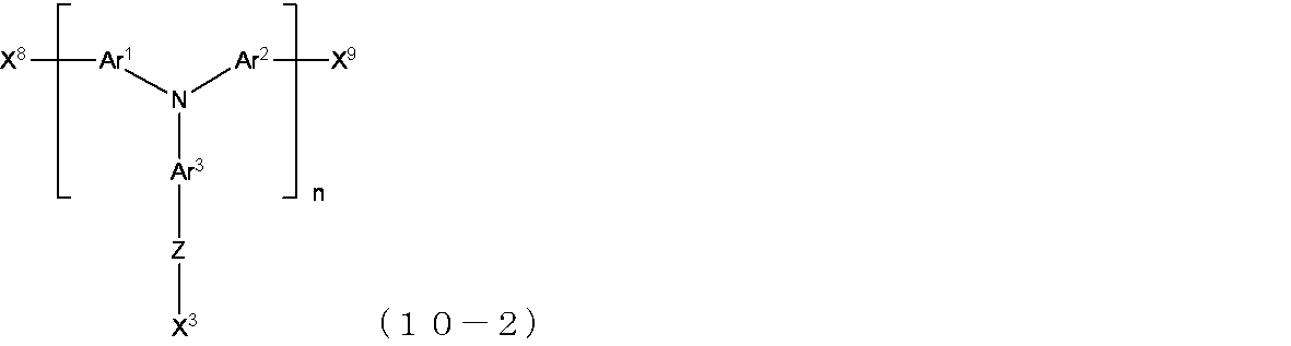
官能基群:-B(OR5)(OR6)(式中、R5及びR6は前記と同じ意味を表す。)
上記式(10-2)の具体例としては、上記(4b)、(4h)、(4l)、(4y)が挙げられる。
本発明はまた、上記式(9)で表される芳香族化合物中のX3で表される脱離基に、上記式(11-1)で表される窒素化合物を反応させることにより、該芳香族化合物をアンモニウム塩に変換することを含む、上記式(5)で表される構造単位を有する芳香族化合物の製造方法を提供する。
式(11-1)で表される窒素化合物としては、第3級アミン化合物が好ましく用いられる。該窒素化合物の具体例としては、トリメチルアミン、トリエチルアミン、トリ-1-プロピルアミン、トリ-2-プロピルアミン、トリ-n-ブチルアミン、トリ-2-ブチルアミン、トリ-1-ペンチルアミン、トリ-2-ペンチルアミン、トリ-3-ペンチルアミン、トリネオペンチルアミン、トリシクロペンチルアミン、トリ-1-ヘキシルアミン、トリ-2-ヘキシルアミン、トリ-3-ヘキシルアミン、ピリジン、N-メチルイミダゾール、N-メチルピロリジン、N-メチルモルホリン等が挙げられる。
本発明は上記式(9)で表される芳香族化合物が上記式(10)で表される芳香族化合物であり、上記式(5)で表される芳香族化合物が上記式(6)で表される芳香族化合物である、上記製造方法を提供する。
また、本発明は上記式(9)で表される芳香族化合物が上記式(10-1)で表される芳香族化合物であり、上記式(5)で表される芳香族化合物が上記式(6-1)で表される芳香族化合物である、上記製造方法を提供する。更に、本発明は上記式(9)で表される芳香族化合物が上記式(10-1)で表される芳香族化合物であり、上記式(5)で表される芳香族化合物が上記式(6-1)で表される芳香族化合物である、上記製造方法を提供する。
また、本発明は上記式(9)で表される芳香族化合物が上記式(10-1)で表される芳香族化合物であり、上記式(5)で表される芳香族化合物が上記式(6-1)で表される芳香族化合物である、上記製造方法を提供する。更に、本発明は上記式(9)で表される芳香族化合物が上記式(10-1)で表される芳香族化合物であり、上記式(5)で表される芳香族化合物が上記式(6-1)で表される芳香族化合物である、上記製造方法を提供する。
本発明はまた、上記式(10)で表される化合物を用い、sp2炭素-sp2炭素結合形成反応を行い、上記式(9)で表される構造単位の数及び/又は(10)で表される芳香族化合物の上記nを増加させる、製造方法を提供する。この場合、先述の式(3)で表される構造単位を有する芳香族化合物及び/又は式(4)で表される芳香族化合物の製造方法を同様に適用できる。
本発明の芳香族化合物は、本発明の芳香族化合物を含む組成物として使用することもできる。
本発明の芳香族化合物を用いて、本発明の芳香族化合物及び/又はそれを含む組成物からなる膜とすることもできる。
前記において、本発明の実施の形態について説明を行ったが、前記に開示された本発明
の実施の形態は、あくまで例示であって、本発明の範囲はこれらの実施の形態に限定され
ない。本発明の範囲は、特許請求の範囲によって示され、さらに特許請求の範囲の記載と
均等の意味及び範囲内でのすべての変更を含むものである。
の実施の形態は、あくまで例示であって、本発明の範囲はこれらの実施の形態に限定され
ない。本発明の範囲は、特許請求の範囲によって示され、さらに特許請求の範囲の記載と
均等の意味及び範囲内でのすべての変更を含むものである。
以下に実施例を挙げて本発明を説明するが、本発明はこれらの実施例により何ら限定さ
れるものではない。
れるものではない。
実施例1(化合物1の合成)

トリ(4-ブロモフェニル)アミン/THF溶液(0.2mol/L、トリ(4-ブロモフェニル)アミンの含有量は100g、0.21mol)を-60℃(内温、dry ice-acetone bath使用)に冷却し、温度が-55℃以上にならないようにtert-BuLi(1.6mol/Lペンタン溶液、トリ(4-ブロモフェニル)アミンに対して1.5当量)を15分かけて加え、別途-60℃(内温)で用意した1,6-ジブロモヘキサン(1.0mol/L THF溶液、トリ(4-ブロモフェニル)アミンに対して5.0当量)に、シリンジで内温が-55℃以上にならないように数回に分けて加えた。
この反応溶液を冷浴より出し、撹拌を続けながら30分かけて室温に戻した。内温15℃になったところで反応を停止した。溶媒を減圧留去して得られたオイル状物質を、さらに減圧蒸留して残存している1,6-ジブロモヘキサンを除去して粘ちょうな黄色のオイル状物質を得た。これを酢酸エチル500mLに溶解し、0.1mol/L塩酸500mL及び飽和食塩水500mLで洗浄し、無水硫酸ナトリウム上で乾燥した。溶媒を減圧留去して粗生成物115gを得た。
シリカゲルカラムクロマトグラフィー(展開溶媒:酢酸エチル/ヘキサン、体積比1/200から1/40までの直線的な濃度勾配を使用)による精製を行い、化合物1を含む混合物を無色粘稠オイル(26.9g)として得た。この無色粘稠オイルを下記の条件でHPLCに供したところ、化合物1を単離することができた。HPLC面積百分率から、前記混合物中の化合物1の含有量を24.1g(収率21%)と算出した。
この反応溶液を冷浴より出し、撹拌を続けながら30分かけて室温に戻した。内温15℃になったところで反応を停止した。溶媒を減圧留去して得られたオイル状物質を、さらに減圧蒸留して残存している1,6-ジブロモヘキサンを除去して粘ちょうな黄色のオイル状物質を得た。これを酢酸エチル500mLに溶解し、0.1mol/L塩酸500mL及び飽和食塩水500mLで洗浄し、無水硫酸ナトリウム上で乾燥した。溶媒を減圧留去して粗生成物115gを得た。
シリカゲルカラムクロマトグラフィー(展開溶媒:酢酸エチル/ヘキサン、体積比1/200から1/40までの直線的な濃度勾配を使用)による精製を行い、化合物1を含む混合物を無色粘稠オイル(26.9g)として得た。この無色粘稠オイルを下記の条件でHPLCに供したところ、化合物1を単離することができた。HPLC面積百分率から、前記混合物中の化合物1の含有量を24.1g(収率21%)と算出した。
HPLC条件
機種:SPD-10AV/LC-10AT/DGU-3A/SCL-10AVP/SIL-10A/C-R5A(Shimadzu)
カラム:Mightysil RP-18GP(5μm、6mm id、15cm、関東化学)
移動相:アセトニトリル/水=95/5(体積比)、流速1.0mL/min
検出波長:254nm
カラム温度:40℃
機種:SPD-10AV/LC-10AT/DGU-3A/SCL-10AVP/SIL-10A/C-R5A(Shimadzu)
カラム:Mightysil RP-18GP(5μm、6mm id、15cm、関東化学)
移動相:アセトニトリル/水=95/5(体積比)、流速1.0mL/min
検出波長:254nm
カラム温度:40℃
1H-NMR(400MHz、CDCl3、機種:BRUKER ADVANCE 400)
:δ1.3-2.6ppm(m、化合物1の-CH2-)、
3.4ppm(t、化合物1の-CH2Br)、
6.9-7.3ppm(m、化合物1の芳香環)
:δ1.3-2.6ppm(m、化合物1の-CH2-)、
3.4ppm(t、化合物1の-CH2Br)、
6.9-7.3ppm(m、化合物1の芳香環)
ポリマー分子量測定法
ポリスチレン換算の数平均分子量(Mn)及び重量平均分子量(Mw)はサイズ排除クロマトグラフィー(SEC)により次の条件で求めた。
装置:東ソー製HLC-8220GPC
カラム:下記4本のカラムを直列に繋げた。
TSKguardcolumn SuperMPHZ-M(東ソー製)1本
TSKgel SuperMultiporeHZ-M(東ソー製)3本
移動相:テトラヒドロフラン
検出器:示差屈折率検出器
ポリスチレン換算の数平均分子量(Mn)及び重量平均分子量(Mw)はサイズ排除クロマトグラフィー(SEC)により次の条件で求めた。
装置:東ソー製HLC-8220GPC
カラム:下記4本のカラムを直列に繋げた。
TSKguardcolumn SuperMPHZ-M(東ソー製)1本
TSKgel SuperMultiporeHZ-M(東ソー製)3本
移動相:テトラヒドロフラン
検出器:示差屈折率検出器
実施例2(化合物2の合成)
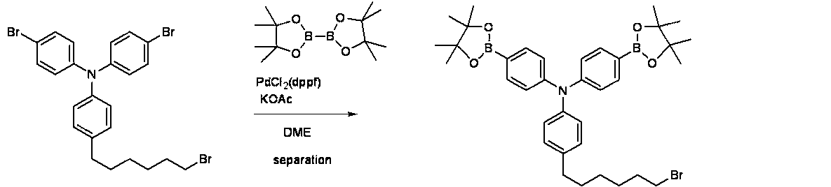
化合物1(実施例1記載の混合物を12.5g用いた。純分として11.3g=0.20mmol)の1,2-ジメトキシエタン溶液300mLを30分間窒素バブリングし、ビス(ピナコラート)ジボロン 27.7g(109mmol)、及び酢酸カリウム(48.3g、493mmol)を加えてよく攪拌し、ここへPdCl2(dppf)/CH2Cl2溶液(PdCl2(dppf)の含有量は1.0g、1.2mmol)を加え、80℃で2時間攪拌した。23℃に戻した反応液を水1500mLに投入し、酢酸エチル250mLで3回抽出した。酢酸エチル層を合一し飽和食塩水500mLで洗浄した後、無水硫酸ナトリウム上で乾燥した。溶媒を減圧留去して得られた混合物をシリカゲルカラムクロマトグラフィー(展開溶媒:酢酸エチル/ヘキサン、体積比1/100から1/10までの直線的な濃度勾配を使用)により精製し、化合物2を8.3g得た(白色固体、収率65%、HPLCから純度100%)。
なお、HPLC条件、NMR条件は化合物1と同一である。
なお、HPLC条件、NMR条件は化合物1と同一である。
1H-NMR(400MHz、CDCl3)
:δ1.3ppm(s、24H、-CH3)、
1.3-2.6ppm(m、10H、-CH2-)、
3.4ppm(t、2H、-CH2Br)、
7.0-7.7ppm(m、化合物2の12H、芳香環)
:δ1.3ppm(s、24H、-CH3)、
1.3-2.6ppm(m、10H、-CH2-)、
3.4ppm(t、2H、-CH2Br)、
7.0-7.7ppm(m、化合物2の12H、芳香環)
実施例3(第4級アンモニウム塩化)
実施例1において得られた、化合物1を含む混合物を、トリエチルアミンと反応させれば、化合物1を第4級アンモニウム塩化合物(化合物3)に変換することができる。
実施例1において得られた、化合物1を含む混合物を、トリエチルアミンと反応させれば、化合物1を第4級アンモニウム塩化合物(化合物3)に変換することができる。
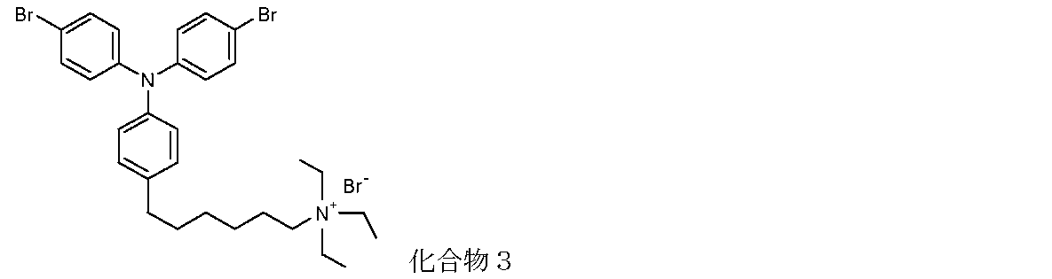
実施例4(化合物2の高分子化)
実施例2において得られた化合物2とほぼ等モル量のアリーレンジハライド化合物との間でSuzukiカップリングによる縮重合をPd(PPh3)4及びアルカリの存在下で行えば、ブロモアルキル基を有するポリマーが得られる。該ポリマーをトリエチルアミンと反応させれば、第4級アンモニウム塩を有するポリマーに変換できる。該ポリマーは正孔注入材料として用いることができる。
実施例2において得られた化合物2とほぼ等モル量のアリーレンジハライド化合物との間でSuzukiカップリングによる縮重合をPd(PPh3)4及びアルカリの存在下で行えば、ブロモアルキル基を有するポリマーが得られる。該ポリマーをトリエチルアミンと反応させれば、第4級アンモニウム塩を有するポリマーに変換できる。該ポリマーは正孔注入材料として用いることができる。
実施例5(化合物3の高分子化)
実施例3において得られる化合物3同士で、Ni(0)触媒によるカップリング反応にて縮重合を行えば、第4級アンモニウム塩を有するポリマーが得られる。該ポリマーは正孔注入材料として用いることができる。
実施例3において得られる化合物3同士で、Ni(0)触媒によるカップリング反応にて縮重合を行えば、第4級アンモニウム塩を有するポリマーが得られる。該ポリマーは正孔注入材料として用いることができる。
実施例6(化合物2の共重合による、ブロモアルキル基を有するポリマーの合成)
三口丸底フラスコを用い、窒素雰囲気中23℃にて、実施例2において得られた化合物2 0.98g(1.48mmol)と2,5-ジメトキシ-1,4-ジブロモベンゼン 0.46g(Aldrich製、1.50mmol)をTHF86mlに溶解し、得られた溶液を40分間窒素バブリングした。バブリング終了後、該溶液を80℃のオイルバスに浸漬し80℃まで昇温した。続いて該溶液にテトラキストリフェニルホスフィンパラジウムPd(PPh3)4 0.019g(Aldrich製、0.016mmol)を加えて反応混合物を得た。
炭酸カリウム1.02g(和光純薬製、7.4mmol)を純水12mlに溶解し、40分間窒素バブリングして得た溶液を、上記反応混合物に15分間かけて滴下した。その後、オイルバスの温度を80℃に保ち、7時間攪拌した。反応混合物には固形分の析出は認められず、各成分は完溶していた。
反応混合物を23℃まで冷却し、40分間窒素バブリングした後、該反応混合物にフェニルボロン酸0.018g(Aldrich製、0.15mmol)を添加した。得られた混合物を80℃のオイルバスに浸漬し、80℃まで昇温した。続いて該混合物にテトラキストリフェニルホスフィンパラジウムPd(PPh3)4 0.018g(Aldrich製、0.016mmol)を添加して9時間攪拌した。
得られた反応混合物を23℃まで冷却し、大過剰のメタノール:水=400ml:100ml混合液に滴下した。析出したポリマーを吸引ろ過で分離した後、メタノール:水=4:1(体積比)溶液で洗浄し、真空乾燥して、ポリマー0.62g(収率77%)を得た。
三口丸底フラスコを用い、窒素雰囲気中23℃にて、実施例2において得られた化合物2 0.98g(1.48mmol)と2,5-ジメトキシ-1,4-ジブロモベンゼン 0.46g(Aldrich製、1.50mmol)をTHF86mlに溶解し、得られた溶液を40分間窒素バブリングした。バブリング終了後、該溶液を80℃のオイルバスに浸漬し80℃まで昇温した。続いて該溶液にテトラキストリフェニルホスフィンパラジウムPd(PPh3)4 0.019g(Aldrich製、0.016mmol)を加えて反応混合物を得た。
炭酸カリウム1.02g(和光純薬製、7.4mmol)を純水12mlに溶解し、40分間窒素バブリングして得た溶液を、上記反応混合物に15分間かけて滴下した。その後、オイルバスの温度を80℃に保ち、7時間攪拌した。反応混合物には固形分の析出は認められず、各成分は完溶していた。
反応混合物を23℃まで冷却し、40分間窒素バブリングした後、該反応混合物にフェニルボロン酸0.018g(Aldrich製、0.15mmol)を添加した。得られた混合物を80℃のオイルバスに浸漬し、80℃まで昇温した。続いて該混合物にテトラキストリフェニルホスフィンパラジウムPd(PPh3)4 0.018g(Aldrich製、0.016mmol)を添加して9時間攪拌した。
得られた反応混合物を23℃まで冷却し、大過剰のメタノール:水=400ml:100ml混合液に滴下した。析出したポリマーを吸引ろ過で分離した後、メタノール:水=4:1(体積比)溶液で洗浄し、真空乾燥して、ポリマー0.62g(収率77%)を得た。
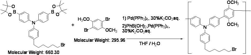
1H-NMR(300MHz、CDCl3)
:δ1.3-1.9ppm(m、8H、-CH2-)、
2.6ppm(t、2H、-CH2-Ar)、
3.4ppm(t、2H、-CH2Br)、
4.8ppm(s、6H、-OCH3)、
6.8-7.7ppm(m、14H、芳香環)
SEC
Mn=4.7×10³
Mw=6.3×10³
:δ1.3-1.9ppm(m、8H、-CH2-)、
2.6ppm(t、2H、-CH2-Ar)、
3.4ppm(t、2H、-CH2Br)、
4.8ppm(s、6H、-OCH3)、
6.8-7.7ppm(m、14H、芳香環)
SEC
Mn=4.7×10³
Mw=6.3×10³
実施例7(化合物2の共重合による、ブロモアルキル基を有するポリマーの合成)
三口丸底フラスコを用い、窒素雰囲気中23℃にて、実施例2において得られた化合物2 0.164g(0.247mmol)と1,3-ジブロモベンゼン 0.059g(東京化成工業製、0.250mmol)をTHF16mlに溶解し、得られた溶液を40分窒素バブリングした。バブリング終了後、該溶液を80℃のオイルバスに浸漬し80℃まで昇温した。続いて該溶液にテトラキストリフェニルホスフィンパラジウムPd(PPh3)4 0.0029g(Aldrich製、0.0025mmol)を加えて反応混合物を得た。
炭酸カリウム0.17g(和光純薬製、1.23mmol)を純水12mlに溶解し、40分間窒素バブリングして得た溶液を、上記反応混合物に15分間かけて滴下した。その後、オイルバスの温度を80℃に保ち、6時間攪拌した。反応混合物には固形分の析出は認められず、各成分は完溶していた。
反応混合物を23℃まで冷却し、40分間窒素バブリングした後、該反応混合物にフェニルボロン酸0.0030g(Aldrich製、0.025mmol)を添加した。得られた混合物を80℃のオイルバスに浸漬し、80℃まで昇温した。続いて該混合物にテトラキストリフェニルホスフィンパラジウムPd(PPh3)4 0.0029g(Aldrich製、0.0025mmol)を添加して9時間攪拌した。
得られた反応混合物を23℃まで冷却し、大過剰のメタノール:水=100ml:20ml混合液に滴下した。析出したポリマーを吸引ろ過で分離した後、メタノール:水=4:1(体積比)溶液で洗浄し、真空乾燥して、ポリマー0.077g(収率64%)を得た。
三口丸底フラスコを用い、窒素雰囲気中23℃にて、実施例2において得られた化合物2 0.164g(0.247mmol)と1,3-ジブロモベンゼン 0.059g(東京化成工業製、0.250mmol)をTHF16mlに溶解し、得られた溶液を40分窒素バブリングした。バブリング終了後、該溶液を80℃のオイルバスに浸漬し80℃まで昇温した。続いて該溶液にテトラキストリフェニルホスフィンパラジウムPd(PPh3)4 0.0029g(Aldrich製、0.0025mmol)を加えて反応混合物を得た。
炭酸カリウム0.17g(和光純薬製、1.23mmol)を純水12mlに溶解し、40分間窒素バブリングして得た溶液を、上記反応混合物に15分間かけて滴下した。その後、オイルバスの温度を80℃に保ち、6時間攪拌した。反応混合物には固形分の析出は認められず、各成分は完溶していた。
反応混合物を23℃まで冷却し、40分間窒素バブリングした後、該反応混合物にフェニルボロン酸0.0030g(Aldrich製、0.025mmol)を添加した。得られた混合物を80℃のオイルバスに浸漬し、80℃まで昇温した。続いて該混合物にテトラキストリフェニルホスフィンパラジウムPd(PPh3)4 0.0029g(Aldrich製、0.0025mmol)を添加して9時間攪拌した。
得られた反応混合物を23℃まで冷却し、大過剰のメタノール:水=100ml:20ml混合液に滴下した。析出したポリマーを吸引ろ過で分離した後、メタノール:水=4:1(体積比)溶液で洗浄し、真空乾燥して、ポリマー0.077g(収率64%)を得た。
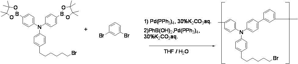
1H-NMR(300MHz、CDCl3)
:δ1.2-2.0ppm(m、8H、-CH2-)、
2.6ppm(t、2H、-CH2-Ar)、
3.4ppm(t、2H、-CH2Br)、、
6.8-7.9ppm(m、14H、芳香環)
:δ1.2-2.0ppm(m、8H、-CH2-)、
2.6ppm(t、2H、-CH2-Ar)、
3.4ppm(t、2H、-CH2Br)、、
6.8-7.9ppm(m、14H、芳香環)
実施例8(実施例6記載のポリマーの、第4級アンモニウム塩への変換)
実施例6記載の方法にて得たにて得られたポリマー0.70g(繰り返し構造単位基準で1.23mmol)をトリメチルアミンの4.2mol/Lエタノール溶液30ml(Aldrich製、126mmol)中に分散させ、23℃で3日間攪拌した。得られた反応混合物から溶媒を留去し、減圧乾燥して4級アンモニウム塩ポリマーを0.71g(収率96%)得た。得られたポリマーはメタノールに10重量%で溶解することを確認した。
実施例6記載の方法にて得たにて得られたポリマー0.70g(繰り返し構造単位基準で1.23mmol)をトリメチルアミンの4.2mol/Lエタノール溶液30ml(Aldrich製、126mmol)中に分散させ、23℃で3日間攪拌した。得られた反応混合物から溶媒を留去し、減圧乾燥して4級アンモニウム塩ポリマーを0.71g(収率96%)得た。得られたポリマーはメタノールに10重量%で溶解することを確認した。
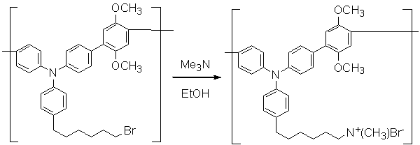
1H-NMR(300MHz、DMSO-d6)
:δ1.3-1.9ppm(m、8H、-CH2-)、
2.3ppm(t、2H、-CH2-Ar)、
3.1ppm(s、9H、-N+(CH3)3、
3.4ppm(s、2H、-CH2N+)、
3.7-4.0ppm(m、6H、-OCH3)、
6.8-7.7ppm(m、14H、芳香環)
元素分析(Nはフラスコ燃焼法で、Brはフラスコ燃焼‐イオンクロマトグラフ法で測定。以下同様)
N : 4.2重量% (計算値: 4.5重量%)
Br:13.8重量% (計算値:12.9重量%)
:δ1.3-1.9ppm(m、8H、-CH2-)、
2.3ppm(t、2H、-CH2-Ar)、
3.1ppm(s、9H、-N+(CH3)3、
3.4ppm(s、2H、-CH2N+)、
3.7-4.0ppm(m、6H、-OCH3)、
6.8-7.7ppm(m、14H、芳香環)
元素分析(Nはフラスコ燃焼法で、Brはフラスコ燃焼‐イオンクロマトグラフ法で測定。以下同様)
N : 4.2重量% (計算値: 4.5重量%)
Br:13.8重量% (計算値:12.9重量%)
実施例9(実施例8記載の第4級アンモニウム塩のカウンターアニオンの交換)
実施例8記載の方法にて合成したポリマー0.30g(繰り返し構造単位基準で486mmol)を窒素雰囲気下25℃でN,N-ジメチルホルムアミド(和光純薬製)3.0mlに溶解し、得られた溶液にトリフルオロメタンスルホン酸ナトリウム0.11g(631mmol、和光純薬製)を加え、10時間攪拌した。反応溶液をイオン交換水100mlに滴下し、析出したポリマーを吸引ろ過で取り出した。得られたポリマーを50mlのイオン交換水中に分散させて攪拌して洗浄し、吸引ろ過してポリマーを取り出した。これを2回繰り返した後、得られたポリマーを40℃で減圧乾燥して、トリフルオロメタンスルホン酸アニオンを導入した第4級アンモニウム塩ポリマー0.18gを得た。
元素分析の結果から、ブロモアニオンの70モル%がトリフルオロメタンスルホン酸アニオンに置換された、下記の組成式で表されるポリマーが得られたことが判明した。なおナトリウム分は検出されなかったことから、余剰のトリフルオロメタンスルホン酸ナトリウムは取り出し工程で除去されたことがわかった。
実施例8記載の方法にて合成したポリマー0.30g(繰り返し構造単位基準で486mmol)を窒素雰囲気下25℃でN,N-ジメチルホルムアミド(和光純薬製)3.0mlに溶解し、得られた溶液にトリフルオロメタンスルホン酸ナトリウム0.11g(631mmol、和光純薬製)を加え、10時間攪拌した。反応溶液をイオン交換水100mlに滴下し、析出したポリマーを吸引ろ過で取り出した。得られたポリマーを50mlのイオン交換水中に分散させて攪拌して洗浄し、吸引ろ過してポリマーを取り出した。これを2回繰り返した後、得られたポリマーを40℃で減圧乾燥して、トリフルオロメタンスルホン酸アニオンを導入した第4級アンモニウム塩ポリマー0.18gを得た。
元素分析の結果から、ブロモアニオンの70モル%がトリフルオロメタンスルホン酸アニオンに置換された、下記の組成式で表されるポリマーが得られたことが判明した。なおナトリウム分は検出されなかったことから、余剰のトリフルオロメタンスルホン酸ナトリウムは取り出し工程で除去されたことがわかった。

1H-NMR(300MHz、DMSO-d6)
:δ1.3-1.9ppm(m、8H、-CH2-)、
2.6ppm(t、2H、-CH2-Ar)、
3.1ppm(s、9H、-N+(CH3)3、
3.3ppm(t、2H、-CH2N+)、
3.7-4.0ppm(m、6H、-OCH3)、
7.0-7.6ppm(m、14H、芳香環)
19F-NMR(280MHz、DMSO-d6)
:δ-78ppm(s、3F、-CF3)
元素分析(Fはフラスコ燃焼‐イオンクロマトグラフ法で、Naは硫硝酸分解-塩酸溶解-ICP発光分析法で測定)
N :4.0重量% (計算値:4.2重量%)
Br:4.7重量% (計算値:3.6重量%)
F :5.8重量% (計算値:6.0重量%)
Na:0.0重量% (計算値:0.0重量%)
:δ1.3-1.9ppm(m、8H、-CH2-)、
2.6ppm(t、2H、-CH2-Ar)、
3.1ppm(s、9H、-N+(CH3)3、
3.3ppm(t、2H、-CH2N+)、
3.7-4.0ppm(m、6H、-OCH3)、
7.0-7.6ppm(m、14H、芳香環)
19F-NMR(280MHz、DMSO-d6)
:δ-78ppm(s、3F、-CF3)
元素分析(Fはフラスコ燃焼‐イオンクロマトグラフ法で、Naは硫硝酸分解-塩酸溶解-ICP発光分析法で測定)
N :4.0重量% (計算値:4.2重量%)
Br:4.7重量% (計算値:3.6重量%)
F :5.8重量% (計算値:6.0重量%)
Na:0.0重量% (計算値:0.0重量%)
実施例8及び9記載のポリマーのHOMO-LUMO測定を行った。ガラス基板上にポリマー溶液をスピンコートした。
測定方法:
重合体の最高占有分子軌道(HOMO)の軌道エネルギーは、重合体のイオン化ポテンシャルを測定し、得られたイオン化ポテンシャルを該軌道エネルギーとすることにより求めた。一方、重合体の最低非占有分子軌道(LUMO)の軌道エネルギーは、HOMOとLUMOとのエネルギー差を求め、その値と前記で測定したイオン化ポテンシャルとの和を該軌道エネルギーとすることにより求めた。イオン化ポテンシャルの測定には光電子分光装置(理研計器株式会社製:AC-2)を用いた。また、HOMOとLUMOのエネルギー差は紫外・可視・近赤外分光光度計(Varian社製:Cary5E)を用いて重合体の吸収スペクトルを測定し、その吸収末端より求めた。
実施例8のポリマー:HOMO -5.18eV、LUMO -2.31eV
実施例9のポリマー:HOMO -5.35eV、LUMO -2.47eV
測定方法:
重合体の最高占有分子軌道(HOMO)の軌道エネルギーは、重合体のイオン化ポテンシャルを測定し、得られたイオン化ポテンシャルを該軌道エネルギーとすることにより求めた。一方、重合体の最低非占有分子軌道(LUMO)の軌道エネルギーは、HOMOとLUMOとのエネルギー差を求め、その値と前記で測定したイオン化ポテンシャルとの和を該軌道エネルギーとすることにより求めた。イオン化ポテンシャルの測定には光電子分光装置(理研計器株式会社製:AC-2)を用いた。また、HOMOとLUMOのエネルギー差は紫外・可視・近赤外分光光度計(Varian社製:Cary5E)を用いて重合体の吸収スペクトルを測定し、その吸収末端より求めた。
実施例8のポリマー:HOMO -5.18eV、LUMO -2.31eV
実施例9のポリマー:HOMO -5.35eV、LUMO -2.47eV
実施例10又は11(実施例8又は9記載のポリマーの正孔注入性評価)
ホールオンリーデバイスを作製し実施例8又は9記載のポリマー正孔注入性を評価した。素子構造は以下の構成とした。
ITO/実施例8又は9記載のポリマーからなる正孔注入・輸送層(30~40nm)/正孔輸送層である中間層(100nm)/Au(100nm)
ホールオンリーデバイスを作製し実施例8又は9記載のポリマー正孔注入性を評価した。素子構造は以下の構成とした。
ITO/実施例8又は9記載のポリマーからなる正孔注入・輸送層(30~40nm)/正孔輸送層である中間層(100nm)/Au(100nm)
実施例10(ホールオンリーデバイス1の作製)
実施例8で合成したポリマー(以下、ポリマー1と呼称することもある)とメタノールを混合し、1.5重量%のポリマー1を含む正孔注入・輸送層形成用組成物を得た。
ガラス基板表面に成膜パターニングされたITO陽極(厚さ:45nm)上に、上記正孔注入・輸送層用組成物を塗布し、スピンコート法によって厚さが30nmになるように正孔注入・輸送層を成膜した。正孔注入・輸送層が成膜されたガラス基板を不活性雰囲気下(窒素雰囲気下)、180℃で10分加熱し、その後、基板を室温まで自然冷却させて、正孔注入・輸送層が形成された基板を得た。
次に、正孔輸送性高分子材料とキシレンとを混合し、0.7重量%の正孔輸送性高分子材料を含む正孔輸送層形成用組成物を得た。
ここで、正孔輸送性高分子材料は、以下の方法で合成した。
不活性ガス雰囲気下、2,7-ジブロモ-9,9-ジ(オクチル)フルオレン(1.4g)、2,7-ビス(4,4,5,5-テトラメチル-1,3,2-ジオキサボロラン-2-イル)-9,9-ジ(オクチル)フルオレン(6.4g)、N,N-ビス(4-ブロモフェニル)-N’,N'-ビス(4-ブチルフェニル)-1,4-フェニレンジアミン(4.1g)、ビス(4-ブロモフェニル)ベンゾシクロブテンアミン(0.6g)、テトラエチルアンモニウムヒドロキシド(1.7g)、酢酸パラジウム(4.5mg)、トリ(2-メトキシフェニル)ホスフィン(0.03g)、及びトルエン(100mL)を混合し、得られた混合物を100℃で2時間加熱攪拌した。次いで、フェニルボロン酸(0.06g)を添加し、得られた混合物を10時間撹拌した。放冷後、水層を除去し、ジエチルジチオカルバミン酸ナトリウム水溶液を添加し攪拌した。その後、水層を除去し、有機層を水、次いで3重量%酢酸水で洗浄した。有機層をメタノールに注いでポリマーを沈殿させた後、濾取したポリマーを再度トルエンに溶解させ、シリカゲル及びアルミナのカラムに通液した。ポリマーを含む溶出トルエン溶液を回収し、回収した前記トルエン溶液をメタノールに注いでポリマーを沈殿させた。沈殿したポリマーを濾取後50℃で真空乾燥し、正孔輸送性高分子材料を得た。正孔輸送性高分子材料のポリスチレン換算の重量平均分子量は3.0×105であった。
不活性ガス雰囲気下、2,7-ジブロモ-9,9-ジ(オクチル)フルオレン(1.4g)、2,7-ビス(4,4,5,5-テトラメチル-1,3,2-ジオキサボロラン-2-イル)-9,9-ジ(オクチル)フルオレン(6.4g)、N,N-ビス(4-ブロモフェニル)-N’,N'-ビス(4-ブチルフェニル)-1,4-フェニレンジアミン(4.1g)、ビス(4-ブロモフェニル)ベンゾシクロブテンアミン(0.6g)、テトラエチルアンモニウムヒドロキシド(1.7g)、酢酸パラジウム(4.5mg)、トリ(2-メトキシフェニル)ホスフィン(0.03g)、及びトルエン(100mL)を混合し、得られた混合物を100℃で2時間加熱攪拌した。次いで、フェニルボロン酸(0.06g)を添加し、得られた混合物を10時間撹拌した。放冷後、水層を除去し、ジエチルジチオカルバミン酸ナトリウム水溶液を添加し攪拌した。その後、水層を除去し、有機層を水、次いで3重量%酢酸水で洗浄した。有機層をメタノールに注いでポリマーを沈殿させた後、濾取したポリマーを再度トルエンに溶解させ、シリカゲル及びアルミナのカラムに通液した。ポリマーを含む溶出トルエン溶液を回収し、回収した前記トルエン溶液をメタノールに注いでポリマーを沈殿させた。沈殿したポリマーを濾取後50℃で真空乾燥し、正孔輸送性高分子材料を得た。正孔輸送性高分子材料のポリスチレン換算の重量平均分子量は3.0×105であった。
上記で得た正孔注入・輸送層が形成された基板の正孔注入・輸送層の上に、正孔輸送層形成用組成物をスピンコート法により塗布し、厚さ100nmの塗膜を得た。この塗膜を設けた基板を不活性雰囲気下(窒素雰囲気下)、180℃で10分間加熱し、塗膜を不溶化させた後、基板を室温まで自然冷却させ、正孔輸送層が形成された基板を得た。
上記で得た正孔輸送層が形成された基板を真空装置内に挿入し、真空蒸着法によって該層の上にAuを100nm成膜し、陰極を形成させて、積層構造体1を製造した。
上記で得た積層構造体1を真空装置より取り出し、不活性雰囲気下(窒素雰囲気下)で、封止ガラスと2液混合型エポキシ樹脂にて封止し、ホールオンリーデバイス1を得た。
実施例11(ホールオンリーデバイス2の作製)
実施例9で合成したポリマー(以下、ポリマー2と呼称することがある)とメタノールを混合し、1.5重量%のポリマー2を含む正孔注入・輸送層形成用組成物を得た。
ガラス基板表面に成膜パターニングされたITO陽極(厚さ:45nm)上に、上記正孔注入・輸送層用組成物を塗布し、スピンコート法によって厚さが40nmになるように正孔注入・輸送層を成膜した。正孔注入・輸送層が成膜されたガラス基板を不活性雰囲気下(窒素雰囲気下)、180℃で60分加熱し、その後、基板を室温まで自然冷却させて、正孔注入・輸送層が形成された基板を得た。
次に、正孔輸送性高分子材料とキシレンとを混合し、0.7重量%の正孔輸送性高分子材料を含む正孔輸送層形成用組成物を得た。ここで、正孔輸送性高分子材料は、実施例10記載の方法で合成したものであり、そのポリスチレン換算の重量平均分子量は3.0×10⁵であった。
上記で得た正孔注入・輸送層が形成された基板の正孔注入・輸送層の上に、正孔輸送層形成用組成物をスピンコート法により塗布し、厚さ100nmの塗膜を得た。この塗膜を設けた基板を不活性雰囲気下(窒素雰囲気下)、180℃で10分間加熱し、塗膜を不溶化させた後、基板を室温まで自然冷却させ、正孔輸送層が形成された基板を得た。
上記で得た正孔輸送層が形成された基板を真空装置内に挿入し、真空蒸着法によって該層の上にAuを100nm成膜し、陰極を形成させて、積層構造体2を製造した。
上記で得た積層構造体2を真空装置より取り出し、不活性雰囲気下(窒素雰囲気下)で、封止ガラスと2液混合型エポキシ樹脂にて封止し、ホールオンリーデバイス2を得た。
比較例1(ホールオンリーデバイスC1の作製)
実施例10において、正孔注入・輸送層を形成させない以外は、実施例10と同様に操作し、ホールオンリーデバイスC1を得た。
実施例10において、正孔注入・輸送層を形成させない以外は、実施例10と同様に操作し、ホールオンリーデバイスC1を得た。
[測定]
上記で得られたホールオンリ-デバイス1、2、及びC1に4.0Vの逆方向電圧を印加し、電流密度を測定した。結果を表1に示す。
上記で得られたホールオンリ-デバイス1、2、及びC1に4.0Vの逆方向電圧を印加し、電流密度を測定した。結果を表1に示す。

表1から明らかなように、本発明の芳香族化合物を含むホールオンリーデバイスは、前記芳香族化合物を含まないホールオンリーデバイスに比べ、電流密度が優れる。
以上より、オニウムイオン、特に第1級~第4級アンモニウムイオンの少なくとも1種、とりわけ第4級アンモニウムイオンを炭化水素側鎖、特にアルキル側鎖に有する本発明の芳香族化合物は、積層構造体及び電子デバイスに応用でき、とりわけ、同じ電圧でより高い電流密度を確保できる正孔注入材料として好適に利用でき、極めて有用である。
Claims (16)
- 基体と、下記式(1)で表される構造単位を有する芳香族化合物を含む正孔注入及び/又は正孔輸送層とを有する積層構造体。

-N+R1R2R3 (2-1)
-P+R1R2R3 (2-2)
-S+R1R2 (2-3)
(式(2-1)、(2-2)及び(2-3)の各々において、R1、R2及びR3はそれぞれ独立に、水素原子、又は置換基を有していてもよい1価の炭化水素基を表し、但し、R1、R2及びR3の少なくとも2個が互いに結合して少なくとも1個の環を形成していてもよい。) - 前記正孔注入及び/又は正孔輸送層が架橋構造を有する請求項1記載の積層構造体。
- 請求項1又は2記載の積層構造体を有する電子デバイス。
- 下記式(3)で表される構造単位を有する芳香族化合物。

-N+R1R2R3 (2-1)
-P+R1R2R3 (2-2)
-S+R1R2 (2-3)
(式(2-1)、(2-2)及び(2-3)の各々において、R1、R2及びR3はそれぞれ独立に、水素原子、又は置換基を有していてもよい1価の炭化水素基を表し、但し、R1、R2及びR3の少なくとも2個が互いに結合して少なくとも1個の環を形成していてもよい。) - 下記式(4)で表される請求項4記載の芳香族化合物。
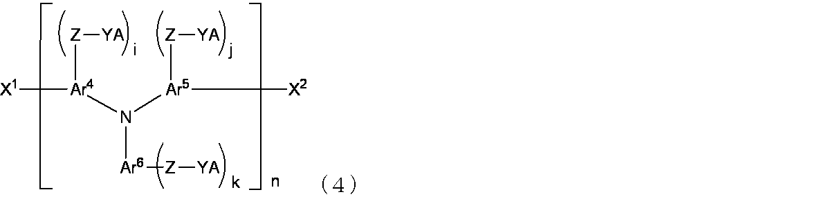
- 下記式(5)で表される構造単位を有する芳香族化合物である請求項4記載の芳香族化合物。
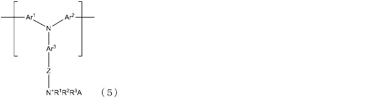
- 下記式(6)で表される請求項6記載の芳香族化合物。

- 下記式(7)で表される構造単位を有する芳香族化合物。
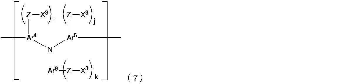
- 下記式(8)で表される請求項8記載の芳香族化合物。

- 下記式(9)で表される構造単位を有する芳香族化合物である請求項8記載の芳香族化合物。
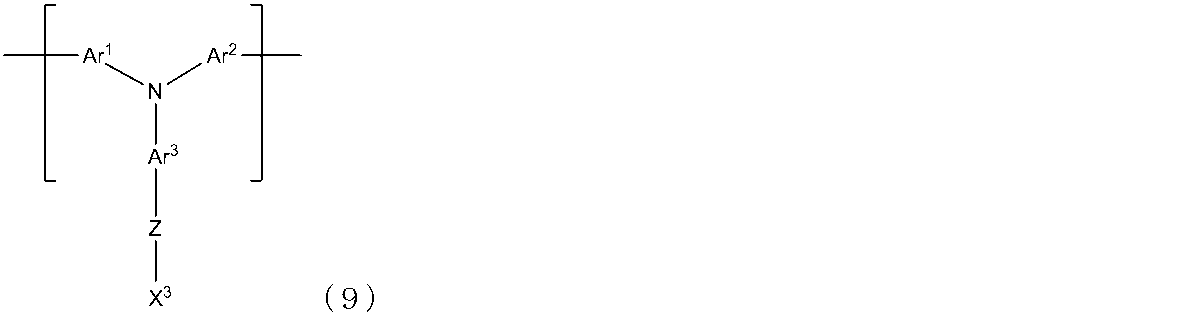
- 下記式(10)で表される請求項10記載の芳香族化合物。
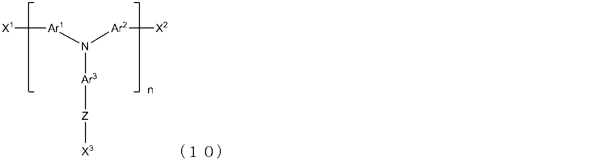
- 式(7)で表される構造単位を有する請求項8記載の芳香族化合物を、下記式(11-1)で表される窒素化合物、下記式(11-2)で表されるリン化合物、下記式(11-3)で表される硫黄化合物又はそれら化合物の2種以上の組み合わせと反応させることにより、該芳香族化合物をそのオニウム塩に変換することを含む式(3)で表される構造単位を有する請求項4記載の芳香族化合物の製造方法。
NR1R2R3 (11-1)
PR1R2R3 (11-2)
SR1R2 (11-3)
(式(11-1)、(11-2)及び(11-3)の各々において、R1、R2及びR3はそれぞれ独立に、水素原子、又は置換基を有していてもよい1価の炭化水素基を表し、但し、R1、R2及びR3の少なくとも2個が互いに結合して少なくとも1個の環を形成していてもよい。) - 式(7)で表される構造単位を有する請求項8記載の芳香族化合物が式(8)で表される請求項9記載の芳香族化合物であり、式(3)で表される構造単位を有する請求項4記載の芳香族化合物が式(4)で表される請求項5記載の芳香族化合物である請求項12記載の製造方法。
- 式(7)で表される構造単位を有する請求項8記載の芳香族化合物中のX3で表される脱離基に、前記窒素化合物、前記リン化合物、前記硫黄化合物又はそれら化合物の2種以上の組み合わせを反応させる請求項12記載の製造方法。
- 式(9)で表される構造単位を有する請求項10記載の芳香族化合物中のX3で表される脱離基に、上記式(11-1)で表される窒素化合物を反応させることにより、式(5)で表される構造単位を有する請求項6記載の芳香族化合物を製造する請求項14記載の製造方法。
- 式(9)で表される構造単位を有する請求項10記載の芳香族化合物が式(10)で表される請求項11記載の芳香族化合物であり、式(5)で表される構造単位を有する請求項6記載の芳香族化合物が式(6)で表される請求項7記載の芳香族化合物である請求項15記載の製造方法。
Priority Applications (1)
| Application Number | Priority Date | Filing Date | Title |
|---|---|---|---|
| US13/812,678 US9184388B2 (en) | 2010-07-29 | 2011-07-29 | Layered structure, electronic device using same, aromatic compound, and method for manufacturing said compound |
Applications Claiming Priority (2)
| Application Number | Priority Date | Filing Date | Title |
|---|---|---|---|
| JP2010170252 | 2010-07-29 | ||
| JP2010-170252 | 2010-07-29 |
Publications (1)
| Publication Number | Publication Date |
|---|---|
| WO2012015052A1 true WO2012015052A1 (ja) | 2012-02-02 |
Family
ID=45530250
Family Applications (1)
| Application Number | Title | Priority Date | Filing Date |
|---|---|---|---|
| PCT/JP2011/067550 Ceased WO2012015052A1 (ja) | 2010-07-29 | 2011-07-29 | 積層構造体、それを用いた電子デバイス、芳香族化合物及び該化合物の製造方法 |
Country Status (4)
| Country | Link |
|---|---|
| US (1) | US9184388B2 (ja) |
| JP (1) | JP5866157B2 (ja) |
| TW (1) | TW201211100A (ja) |
| WO (1) | WO2012015052A1 (ja) |
Cited By (2)
| Publication number | Priority date | Publication date | Assignee | Title |
|---|---|---|---|---|
| JP2017059745A (ja) * | 2015-09-18 | 2017-03-23 | 日立化成株式会社 | 有機エレクトロニクス材料、有機エレクトロニクス素子、及び有機エレクトロルミネセンス素子 |
| WO2018016413A1 (ja) * | 2016-07-21 | 2018-01-25 | 住友化学株式会社 | 高分子化合物の製造方法 |
Families Citing this family (2)
| Publication number | Priority date | Publication date | Assignee | Title |
|---|---|---|---|---|
| JP6155611B2 (ja) * | 2012-11-30 | 2017-07-05 | 日立化成株式会社 | 有機エレクトロニクス素子及びその製造方法 |
| CN107204401A (zh) * | 2017-06-05 | 2017-09-26 | 京东方科技集团股份有限公司 | 一种qled器件及其制作方法 |
Citations (4)
| Publication number | Priority date | Publication date | Assignee | Title |
|---|---|---|---|---|
| JPH08239655A (ja) * | 1995-03-06 | 1996-09-17 | Idemitsu Kosan Co Ltd | 有機エレクトロルミネッセンス素子 |
| WO2006137434A1 (ja) * | 2005-06-22 | 2006-12-28 | Sumitomo Chemical Company, Limited | 高分子材料及び高分子発光素子 |
| JP2007246801A (ja) * | 2006-03-17 | 2007-09-27 | Toyo Ink Mfg Co Ltd | 感エネルギー線酸発生剤、酸の発生方法、および感エネルギー線硬化性組成物 |
| WO2007126929A2 (en) * | 2006-04-17 | 2007-11-08 | The Regents Of The University Of California | Hybrid polymer light-emitting devices |
Family Cites Families (37)
| Publication number | Priority date | Publication date | Assignee | Title |
|---|---|---|---|---|
| US4356429A (en) | 1980-07-17 | 1982-10-26 | Eastman Kodak Company | Organic electroluminescent cell |
| JPS6370257A (ja) | 1986-09-12 | 1988-03-30 | Fuji Xerox Co Ltd | 電子写真用電荷輸送材料 |
| JPS63175860A (ja) | 1987-01-16 | 1988-07-20 | Fuji Xerox Co Ltd | 電子写真感光体 |
| JP2651237B2 (ja) | 1989-02-10 | 1997-09-10 | 出光興産株式会社 | 薄膜エレクトロルミネッセンス素子 |
| US5121029A (en) | 1987-12-11 | 1992-06-09 | Idemitsu Kosan Co., Ltd. | Electroluminescence device having an organic electroluminescent element |
| US5075487A (en) | 1988-11-16 | 1991-12-24 | Fuji Xerox Co., Ltd. | Fluorene derivative |
| JPH02135361A (ja) | 1988-11-16 | 1990-05-24 | Fuji Xerox Co Ltd | 電子写真感光体 |
| US5028505A (en) | 1988-11-16 | 1991-07-02 | Fuji Xerox Co., Ltd. | Electrophotographic photoreceptor |
| JPH02135359A (ja) | 1988-11-16 | 1990-05-24 | Fuji Xerox Co Ltd | 電子写真感光体 |
| US5011757A (en) | 1988-11-16 | 1991-04-30 | Fuji Xerox Co., Ltd. | Electrophotographic photoreceptor containing a fluorene derivative |
| JPH0337992A (ja) | 1989-07-04 | 1991-02-19 | Idemitsu Kosan Co Ltd | 有機エレクトロルミネッセンス素子の製造方法 |
| JPH03152184A (ja) | 1989-11-08 | 1991-06-28 | Nec Corp | 有機薄膜el素子 |
| EP0517542B1 (en) | 1991-06-05 | 1995-08-30 | Sumitomo Chemical Company Limited | Organic electroluminescence devices |
| JPH07110940B2 (ja) | 1991-06-05 | 1995-11-29 | 住友化学工業株式会社 | 有機エレクトロルミネッセンス素子 |
| JPH05263073A (ja) | 1992-03-17 | 1993-10-12 | Sumitomo Chem Co Ltd | 有機エレクトロルミネッセンス素子 |
| DE4436773A1 (de) | 1994-10-14 | 1996-04-18 | Hoechst Ag | Konjugierte Polymere mit Spirozentren und ihre Verwendung als Elektrolumineszenzmaterialien |
| DE4442052A1 (de) | 1994-11-25 | 1996-05-30 | Hoechst Ag | Konjugierte Polymere mit Hetero-Spiroatomen und ihre Verwendung als Elektrolumineszenzmaterialien |
| CN1125865C (zh) | 1995-09-04 | 2003-10-29 | 联邦德国赫彻斯特研究技术两合公司 | 作为电致发光材料的含有三芳基胺单元的聚合物 |
| JP3760491B2 (ja) | 1995-10-16 | 2006-03-29 | 住友化学株式会社 | 高分子蛍光体、その製造方法及び有機エレクトロルミネッセンス素子 |
| DE19652261A1 (de) | 1996-12-16 | 1998-06-18 | Hoechst Ag | Arylsubstituierte Poly(p-arylenvinylene), Verfahren zur Herstellung und deren Verwendung in Elektroluminszenzbauelementen |
| US6309763B1 (en) | 1997-05-21 | 2001-10-30 | The Dow Chemical Company | Fluorene-containing polymers and electroluminescent devices therefrom |
| JPH10324870A (ja) | 1997-05-23 | 1998-12-08 | Sumitomo Chem Co Ltd | 高分子蛍光体および有機エレクトロルミネッセンス素子 |
| TW558561B (en) | 1997-07-22 | 2003-10-21 | Sumitomo Chemical Co | Hole transporting polymer and organic electroluminescence device using the same |
| JP4366727B2 (ja) | 1997-07-22 | 2009-11-18 | 住友化学株式会社 | 正孔輸送性高分子とその製造方法および有機エレクトロルミネッセンス素子 |
| US5777070A (en) | 1997-10-23 | 1998-07-07 | The Dow Chemical Company | Process for preparing conjugated polymers |
| GB9805476D0 (en) | 1998-03-13 | 1998-05-13 | Cambridge Display Tech Ltd | Electroluminescent devices |
| GB2340304A (en) | 1998-08-21 | 2000-02-16 | Cambridge Display Tech Ltd | Organic light emitters |
| DE19846768A1 (de) | 1998-10-10 | 2000-04-20 | Aventis Res & Tech Gmbh & Co | Konjugierte Polymere enthaltend 2,7-Fluorenyleinheiten mit verbesserten Eigenschaften |
| GB2348316A (en) | 1999-03-26 | 2000-09-27 | Cambridge Display Tech Ltd | Organic opto-electronic device |
| TW484341B (en) | 1999-08-03 | 2002-04-21 | Sumitomo Chemical Co | Polymeric fluorescent substance and polymer light emitting device |
| AU7432400A (en) | 1999-09-16 | 2001-04-17 | Cambridge Display Technology Limited | Preparation of benzenediboronic acid via a disilylated aryl-intermediate |
| JP4461762B2 (ja) | 2002-10-30 | 2010-05-12 | 住友化学株式会社 | 高分子化合物およびそれを用いた高分子発光素子 |
| AU2003268752A1 (en) | 2002-10-30 | 2004-05-25 | Sumitomo Chemical Company, Limited | High-molecular compounds and polymerer light emitting devices made by using the same |
| TWI365218B (en) | 2003-11-17 | 2012-06-01 | Sumitomo Chemical Co | Conjugated oligomers or polymers based on crosslinkable arylamine compounds |
| ATE555506T1 (de) | 2004-12-24 | 2012-05-15 | Cdt Oxford Ltd | Licht emittierende einrichtung |
| JP5217153B2 (ja) | 2005-11-18 | 2013-06-19 | 住友化学株式会社 | 高分子化合物およびそれを用いた高分子発光素子 |
| US20100176377A1 (en) | 2005-11-18 | 2010-07-15 | Sumitomo Chemical Company, Limited | Polymeric compound and polymeric electroluminescence element using the same |
-
2011
- 2011-07-29 JP JP2011167786A patent/JP5866157B2/ja active Active
- 2011-07-29 US US13/812,678 patent/US9184388B2/en active Active
- 2011-07-29 WO PCT/JP2011/067550 patent/WO2012015052A1/ja not_active Ceased
- 2011-07-29 TW TW100127188A patent/TW201211100A/zh unknown
Patent Citations (4)
| Publication number | Priority date | Publication date | Assignee | Title |
|---|---|---|---|---|
| JPH08239655A (ja) * | 1995-03-06 | 1996-09-17 | Idemitsu Kosan Co Ltd | 有機エレクトロルミネッセンス素子 |
| WO2006137434A1 (ja) * | 2005-06-22 | 2006-12-28 | Sumitomo Chemical Company, Limited | 高分子材料及び高分子発光素子 |
| JP2007246801A (ja) * | 2006-03-17 | 2007-09-27 | Toyo Ink Mfg Co Ltd | 感エネルギー線酸発生剤、酸の発生方法、および感エネルギー線硬化性組成物 |
| WO2007126929A2 (en) * | 2006-04-17 | 2007-11-08 | The Regents Of The University Of California | Hybrid polymer light-emitting devices |
Cited By (6)
| Publication number | Priority date | Publication date | Assignee | Title |
|---|---|---|---|---|
| JP2017059745A (ja) * | 2015-09-18 | 2017-03-23 | 日立化成株式会社 | 有機エレクトロニクス材料、有機エレクトロニクス素子、及び有機エレクトロルミネセンス素子 |
| WO2018016413A1 (ja) * | 2016-07-21 | 2018-01-25 | 住友化学株式会社 | 高分子化合物の製造方法 |
| KR20190032426A (ko) * | 2016-07-21 | 2019-03-27 | 스미또모 가가꾸 가부시키가이샤 | 고분자 화합물의 제조 방법 |
| JPWO2018016413A1 (ja) * | 2016-07-21 | 2019-05-09 | 住友化学株式会社 | 高分子化合物の製造方法 |
| KR102259773B1 (ko) | 2016-07-21 | 2021-06-02 | 스미또모 가가꾸 가부시키가이샤 | 고분자 화합물의 제조 방법 |
| JP7067476B2 (ja) | 2016-07-21 | 2022-05-16 | 住友化学株式会社 | 高分子化合物の製造方法 |
Also Published As
| Publication number | Publication date |
|---|---|
| JP2012049524A (ja) | 2012-03-08 |
| TW201211100A (en) | 2012-03-16 |
| US9184388B2 (en) | 2015-11-10 |
| US20130119369A1 (en) | 2013-05-16 |
| JP5866157B2 (ja) | 2016-02-17 |
Similar Documents
| Publication | Publication Date | Title |
|---|---|---|
| CN107207959B (zh) | 在聚合物主链中包含发光重复单元的有机发光聚合物以及具有其的器件 | |
| EP2272894B1 (en) | Polymer compound, reticulated polymer compound produced by crosslinking the polymer compound, composition for organic electroluminescent element, organic electroluminescent element, organic el display, and organic el lighting | |
| KR101817808B1 (ko) | 전기활성 재료 | |
| TWI465478B (zh) | 新穎聚合物 | |
| KR101605213B1 (ko) | 평탄화제 및 소자 | |
| JP5750165B2 (ja) | 化合物 | |
| KR101616149B1 (ko) | 전기활성 재료 | |
| TWI535758B (zh) | 高分子發光元件 | |
| US8466256B2 (en) | Polymer, organic photoelectronic device, and display including the same | |
| CN101652402A (zh) | 含有二氟环戊二酮环与芳香环缩合而成的单元的聚合物以及使用其的有机薄膜及有机薄膜元件 | |
| CN114341144B (zh) | 有机薄膜及其制造方法、有机电致发光元件及其材料、光电转换元件及其材料 | |
| KR102233198B1 (ko) | 방법 및 화합물 | |
| JP6582786B2 (ja) | 組成物、電荷輸送材料、及びインク並びにそれらの利用 | |
| WO2010013725A1 (ja) | 積層構造体、その製造方法、及びそれを含む電子素子 | |
| JP5866157B2 (ja) | 積層構造体、それを用いた電子デバイス、芳香族化合物及び該化合物の製造方法 | |
| JP2012530158A (ja) | 有機発光ダイオード(oled)用のピレン系ポリマー | |
| CN104247073B (zh) | 有机电致发光元件及其制造方法 | |
| US20240279249A1 (en) | Compound, Coating Composition Comprising Same, Organic Light-Emitting Device Using Same, and Manufacturing Method Therefor | |
| JP6264919B2 (ja) | アリールアミンポリマー、その製造方法及びその用途 | |
| Huang et al. | Synthesis and electroluminescent properties of polyfluorene‐based conjugated polymers containing bipolar groups | |
| Yasuda et al. | New luminescent 1, 2, 4-triazole/thiophene alternating copolymers: Synthesis, characterization, and optical properties | |
| JP2008007762A (ja) | 高分子化合物および高分子発光素子 | |
| KR20200089674A (ko) | 유기 박막의 제조 방법, 유기 박막 및 그의 이용 | |
| EP3605633A1 (en) | Organic electronic material, ink composition, organic layer and organic electronic element | |
| KR20190136096A (ko) | 경화성 중합체, 중합액, 도전성 막 및 유기 발광 소자 |
Legal Events
| Date | Code | Title | Description |
|---|---|---|---|
| 121 | Ep: the epo has been informed by wipo that ep was designated in this application |
Ref document number: 11812641 Country of ref document: EP Kind code of ref document: A1 |
|
| WWE | Wipo information: entry into national phase |
Ref document number: 13812678 Country of ref document: US |
|
| NENP | Non-entry into the national phase |
Ref country code: DE |
|
| 122 | Ep: pct application non-entry in european phase |
Ref document number: 11812641 Country of ref document: EP Kind code of ref document: A1 |