WO2012014252A1 - 有機el表示パネルとその製造方法 - Google Patents
有機el表示パネルとその製造方法 Download PDFInfo
- Publication number
- WO2012014252A1 WO2012014252A1 PCT/JP2010/004760 JP2010004760W WO2012014252A1 WO 2012014252 A1 WO2012014252 A1 WO 2012014252A1 JP 2010004760 W JP2010004760 W JP 2010004760W WO 2012014252 A1 WO2012014252 A1 WO 2012014252A1
- Authority
- WO
- WIPO (PCT)
- Prior art keywords
- film
- organic
- layer
- display panel
- resist
- Prior art date
- Legal status (The legal status is an assumption and is not a legal conclusion. Google has not performed a legal analysis and makes no representation as to the accuracy of the status listed.)
- Ceased
Links
Images





Classifications
-
- H—ELECTRICITY
- H10—SEMICONDUCTOR DEVICES; ELECTRIC SOLID-STATE DEVICES NOT OTHERWISE PROVIDED FOR
- H10K—ORGANIC ELECTRIC SOLID-STATE DEVICES
- H10K59/00—Integrated devices, or assemblies of multiple devices, comprising at least one organic light-emitting element covered by group H10K50/00
- H10K59/10—OLED displays
- H10K59/12—Active-matrix OLED [AMOLED] displays
- H10K59/122—Pixel-defining structures or layers, e.g. banks
-
- H—ELECTRICITY
- H10—SEMICONDUCTOR DEVICES; ELECTRIC SOLID-STATE DEVICES NOT OTHERWISE PROVIDED FOR
- H10K—ORGANIC ELECTRIC SOLID-STATE DEVICES
- H10K10/00—Organic devices specially adapted for rectifying, amplifying, oscillating or switching; Organic capacitors or resistors having potential barriers
- H10K10/40—Organic transistors
- H10K10/46—Field-effect transistors, e.g. organic thin-film transistors [OTFT]
-
- H—ELECTRICITY
- H10—SEMICONDUCTOR DEVICES; ELECTRIC SOLID-STATE DEVICES NOT OTHERWISE PROVIDED FOR
- H10K—ORGANIC ELECTRIC SOLID-STATE DEVICES
- H10K50/00—Organic light-emitting devices
- H10K50/30—Organic light-emitting transistors
-
- H—ELECTRICITY
- H10—SEMICONDUCTOR DEVICES; ELECTRIC SOLID-STATE DEVICES NOT OTHERWISE PROVIDED FOR
- H10K—ORGANIC ELECTRIC SOLID-STATE DEVICES
- H10K50/00—Organic light-emitting devices
- H10K50/80—Constructional details
- H10K50/805—Electrodes
- H10K50/81—Anodes
- H10K50/813—Anodes characterised by their shape
-
- H—ELECTRICITY
- H10—SEMICONDUCTOR DEVICES; ELECTRIC SOLID-STATE DEVICES NOT OTHERWISE PROVIDED FOR
- H10K—ORGANIC ELECTRIC SOLID-STATE DEVICES
- H10K50/00—Organic light-emitting devices
- H10K50/80—Constructional details
- H10K50/805—Electrodes
- H10K50/81—Anodes
- H10K50/818—Reflective anodes, e.g. ITO combined with thick metallic layers
-
- H—ELECTRICITY
- H10—SEMICONDUCTOR DEVICES; ELECTRIC SOLID-STATE DEVICES NOT OTHERWISE PROVIDED FOR
- H10K—ORGANIC ELECTRIC SOLID-STATE DEVICES
- H10K59/00—Integrated devices, or assemblies of multiple devices, comprising at least one organic light-emitting element covered by group H10K50/00
- H10K59/10—OLED displays
- H10K59/12—Active-matrix OLED [AMOLED] displays
- H10K59/121—Active-matrix OLED [AMOLED] displays characterised by the geometry or disposition of pixel elements
- H10K59/1213—Active-matrix OLED [AMOLED] displays characterised by the geometry or disposition of pixel elements the pixel elements being TFTs
-
- H—ELECTRICITY
- H10—SEMICONDUCTOR DEVICES; ELECTRIC SOLID-STATE DEVICES NOT OTHERWISE PROVIDED FOR
- H10K—ORGANIC ELECTRIC SOLID-STATE DEVICES
- H10K59/00—Integrated devices, or assemblies of multiple devices, comprising at least one organic light-emitting element covered by group H10K50/00
- H10K59/10—OLED displays
- H10K59/12—Active-matrix OLED [AMOLED] displays
- H10K59/124—Insulating layers formed between TFT elements and OLED elements
-
- H—ELECTRICITY
- H10—SEMICONDUCTOR DEVICES; ELECTRIC SOLID-STATE DEVICES NOT OTHERWISE PROVIDED FOR
- H10K—ORGANIC ELECTRIC SOLID-STATE DEVICES
- H10K59/00—Integrated devices, or assemblies of multiple devices, comprising at least one organic light-emitting element covered by group H10K50/00
- H10K59/30—Devices specially adapted for multicolour light emission
- H10K59/35—Devices specially adapted for multicolour light emission comprising red-green-blue [RGB] subpixels
-
- H—ELECTRICITY
- H10—SEMICONDUCTOR DEVICES; ELECTRIC SOLID-STATE DEVICES NOT OTHERWISE PROVIDED FOR
- H10K—ORGANIC ELECTRIC SOLID-STATE DEVICES
- H10K59/00—Integrated devices, or assemblies of multiple devices, comprising at least one organic light-emitting element covered by group H10K50/00
- H10K59/80—Constructional details
- H10K59/805—Electrodes
- H10K59/8051—Anodes
- H10K59/80515—Anodes characterised by their shape
-
- H—ELECTRICITY
- H10—SEMICONDUCTOR DEVICES; ELECTRIC SOLID-STATE DEVICES NOT OTHERWISE PROVIDED FOR
- H10K—ORGANIC ELECTRIC SOLID-STATE DEVICES
- H10K59/00—Integrated devices, or assemblies of multiple devices, comprising at least one organic light-emitting element covered by group H10K50/00
- H10K59/80—Constructional details
- H10K59/805—Electrodes
- H10K59/8051—Anodes
- H10K59/80518—Reflective anodes, e.g. ITO combined with thick metallic layers
Definitions
- the present invention relates to an organic EL display panel using an organic electroluminescent element (hereinafter referred to as “organic EL element”) and a method for manufacturing the same, and more particularly to a technique for improving the configuration around the anode.
- organic EL element organic electroluminescent element
- the organic EL element is a current-driven light emitting element and has a basic structure in which a light emitting layer containing an organic light emitting material is disposed between an anode and a cathode. During driving, a voltage is applied between the electrodes, and holes injected from the anode and electrons injected from the cathode are recombined in the light emitting layer, and an electroluminescence phenomenon associated therewith is utilized.
- the organic EL element is self-luminous and has high visibility, and is a completely solid element and excellent in impact resistance.
- the organic EL element As a type of the organic EL element, there is a coating type in which an ink containing a high molecular material or a low molecule with good thin film formability is prepared and applied to a substrate by an inkjet method or the like to form a light emitting layer or a charge injection layer .
- an organic EL display panel in which a plurality of coating-type organic EL elements are arranged in a matrix on a substrate on which a TFT wiring portion is formed has been put into practical use as various displays and image display devices.
- each organic EL element is partitioned by a bank (partition) having a predetermined shape.
- a bank partition
- a line bank extends in the column direction of the substrate and is arranged in parallel in the row direction.
- Light emitting elements of the same color are arranged at regular intervals between adjacent banks.
- FIG. 10 shows a part of a manufacturing process of a conventional organic EL display panel.
- the anode (lower electrode) 6X is arranged for each element formation region along the longitudinal (X) direction of the bank 10. There is a gap 11 between adjacent element formation regions.
- an electrode composed of a laminate of a reflective metal film 60 and a transparent conductive film 61 is formed in a long shape.
- the reflective metal film 60 is electrically connected to the feeding electrode 3 of the TFT wiring section through an opening (contact hole 8) formed by dug down the planarizing film 4.
- the contact hole 8 is formed near one end in the X direction of the lower electrode 60 in the non-light emitting region (pixel restricting region), avoiding the light emitting region of the organic EL element.
- an (organic) light emitting layer 7, an upper electrode 9, a sealing layer (not shown) and the like are sequentially formed on the lower electrode 6.
- the film thickness tends to be thin. For this reason, there is a possibility that a short circuit will occur due to the disconnection of the light emitting layer 7, or an abnormal light emission may occur due to the concentration of the electric field in the thin part.
- the region is made of SiON or the like perpendicular to the longitudinal (X) direction of the bank 10 between the transparent conductive film 61 and the light emitting layer 7.
- a pixel regulating layer 66 made of an insulating material is covered. In the region where the pixel restricting layer 66 is provided, it is possible to prevent the light from flowing from the lower electrode 6 and the upper electrode 9 to the light emitting layer 7 during driving, and a certain effect can be expected in the occurrence of light emission unevenness and short circuit due to an electric field abnormality.
- the organic EL display panel having the conventional line bank structure has several problems.
- a process for forming the pixel regulation layer (a sputtering process when the pixel regulation layer is made of SiON) is separately required. For this reason, a dedicated device for performing the process is required, and the manufacturing process may be complicated, which may increase the production cost.
- the pixel restricting layer is composed of a SiON film formed by sputtering or CVD, but these film forming methods do not have sufficient step coverage. For this reason, as shown in the cross-sectional view of FIG. 8, when the transparent conductive film 61 on the reflective metal film 60 has a bowl shape as the edge processing shape of the lower electrode 6x, the gap between the organic EL elements adjacent in the X direction. 11 parts are not completely covered, and the pixel regulation layer may be disconnected.
- the reflective metal film 60 or the transparent conductive film 61 may be short-circuited with the cathode 9 by using the stepped portion as a current path.
- the present invention has been made in view of the above problems, and as a first object, it can be produced at a relatively low cost, prevents short circuit and abnormal light emission without using a pixel regulation layer, and appropriately An organic EL display panel that can be expected to achieve pixel separation and a manufacturing method thereof are provided.
- a second object is to provide an organic EL display panel that can be expected to have good image display performance by forming a light emitting layer with a more uniform film thickness than conventional ones, and a method for manufacturing the same.
- an organic EL display panel includes a substrate, a thin film transistor layer formed over the substrate, an interlayer insulating film disposed over the thin film transistor layer, and an interlayer insulating layer.
- a plurality of partition walls arranged in a line, a plurality of first electrodes disposed in a row between adjacent partition walls among the plurality of partition walls, and each first electrode disposed along the row A light emitting layer formed above the light emitting layer, and a second electrode formed above the light emitting layer, wherein each of the first electrodes is formed by laminating a reflective metal film and a transparent conductive film.
- a single-layer region of a reflective metal film on which the transparent conductive film is not laminated is present at the opposing end of each first electrode facing along the one row, and the reflective metal in the single-layer region.
- the reflective metal film is formed on the surface of the film.
- Metal oxide film derived from metallic material is configured to present.
- a metal oxide film is formed in a single-layer region made of a reflective metal film at the opposite end of each of the two first electrodes (lower electrodes) adjacent in line units. Yes.
- the metal oxide film is interposed between the first electrode and the second electrode (upper electrode). Therefore, when the organic EL display panel is driven, It can be controlled so that no current flows.
- the metal oxide film has the same function as when the pixel restricting layer is formed so as to partition each element formation region (position of the first electrode) along the same line unit. It can be demonstrated.
- FIG. 1 is a partial perspective view illustrating a configuration of an organic EL display panel 100 according to Embodiment 1.
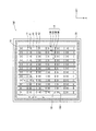
- FIG. 3 is a top view showing a configuration of an organic EL display panel 100.
- FIG. 3 is a partial cross-sectional view showing a configuration of an organic EL display panel 100.
- FIG. It is a fragmentary sectional view which shows the structure of 100 A of organic electroluminescent display panels which have arrange
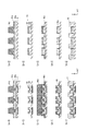
- FIG. It is a figure which shows the manufacturing process around the lower electrode (anode) of this invention. It is a figure which shows the manufacturing process around the lower electrode (anode) of this invention. It is sectional drawing which shows the conventional subject in the case of not providing a pixel control layer.
- FIG. 1 is a diagram illustrating a configuration of an image display device using an organic EL display panel 100.
- FIG. It is the figure which illustrated the utilization form of the image display apparatus.
- An organic EL display panel includes a substrate, a thin film transistor layer formed on the substrate, an interlayer insulating film disposed above the thin film transistor layer, and a plurality of lines arranged in parallel on the interlayer insulating layer.
- a plurality of partition walls a plurality of first electrodes arranged in a row between adjacent partition walls, and a plurality of first electrodes arranged along the row.
- each of the first electrodes including a two-layer region in which a reflective metal film and a transparent conductive film are laminated, There is a single-layer region of the reflective metal film on which the transparent conductive film is not laminated at the opposing end of each first electrode facing along a line, and the reflection metal film surface in the single-layer region has the reflection layer.
- the metal oxide film is formed on the surface of the reflective metal film at least on the end face and the upper surface of the first electrode facing each other in line units.
- the region can be controlled so that no current flows between the first electrode and the second electrode.
- it is possible to avoid the occurrence of abnormal light emission or short circuit due to electric field concentration in the light emitting layer without providing a pixel restricting layer as in the conventional case.
- By disposing such a metal oxide film it is possible to perform the same function as a pixel regulation layer that partitions each organic EL element formed along the same line unit.
- the metal oxide film is not a deposit, but is formed by partially oxidizing a metal material derived from the reflective metal film (so-called surface reaction is caused). Specifically, this metal oxide film can be formed at the same time as the first electrode forming step using an etching process and an ashing process. Therefore, the present invention is excellent in terms of production cost because it is not necessary to separately provide a new process for providing the metal oxide film. Further, according to the present invention, the use of the metal oxide film eliminates the step of forming the pixel restricting layer, so that the production cost can be reduced and the production efficiency can be expected to be improved.
- the pixel regulating layer is not provided between the set of partition walls, when ink of an organic light emitting material is applied, the ink moves over each element formation region between the set of partition walls (mutual flow). can do. Thereby, in the plurality of organic EL elements, the thickness of the light emitting layer can be made uniform.
- the applied ink flows until it dries, it is possible to expect a uniform thickness of the light emitting layer without setting the ink discharge amount so strictly. Thereby, in this invention, the effect which makes easy adjustment of the film thickness of a light emitting layer is acquired.
- the organic light emitting material can move (mutually flow) over a plurality of pixel formation regions. For this reason, in the plurality of organic EL elements, it is possible to make the film thickness of the light emitting layer uniform.
- the organic light emitting material can exhibit fluidity until it is dried, the amount of ink applied during printing does not have to be so strict in order to make the film thickness of each light emitting layer uniform. Therefore, according to the present invention, there is an advantage that the film thickness of the light emitting layer can be easily adjusted.
- the metal oxide film is present in the single layer region at least on the upper surface of the reflective metal film not covered with the partition walls and on the end faces facing each other between the pair of partition walls. It can also be set as the structure to do.
- the metal oxide film When the metal oxide film is formed in this way, the metal oxide film can be present on almost all the surface of the single-layer region of the first electrode that is not covered with the partition walls.
- the short-circuit preventing effect of the two electrodes and the preventing effect of abnormal light emission of the light emitting layer can be obtained satisfactorily.
- the interlayer insulating film is provided with a contact hole for conducting the thin film transistor layer and each of the first electrodes, and an end of each first electrode has a region overlapping with the contact hole.
- the metal oxide film may be in a region overlapping with the contact hole.
- a metal oxide film is formed in a region overlapping with a contact hole in this way, conventionally, the abnormal edge can be satisfactorily obtained by covering the peripheral edge of the contact hole, which is likely to generate abnormal light emission, with the metal oxide film. Generation of light emission can be prevented, which is effective.
- the light emitting layers formed over the first electrodes disposed between the pair of partition walls may have the same color.
- the organic EL display panel of the present invention can be adapted to color display.
- the light emitting layer disposed between each pair of partition walls has a color corresponding to any one of red, green, and blue, and each first electrode between each pair of partition walls.
- the arrangement position of can also be configured to be provided along a direction orthogonal to the longitudinal direction of the partition wall.
- the thickness of the light emitting layer increases from the end of the first electrode toward the central region along the longitudinal direction of the partition wall, and gradually approaches a constant value.
- the length of the single-layer region on the upper surface of the reflective metal film along the direction is at least the thickness of the light-emitting layer from the end portion of the first electrode toward the central region. It can also be set as the length set to reach 90%.
- the metal oxide film formed in the region can be formed at least in the region of the light emitting layer where the film thickness tends to be thin. Therefore, abnormal light emission of the light emitting layer that may occur due to electric field concentration can be effectively prevented by the metal oxide film.
- a configuration in which an adhesion layer exists between the interlayer insulating film and the plurality of first electrodes may be employed.
- the adhesion layer may be composed of any one of titanium, chromium, and conductive metal oxide.
- the reflective metal film can be made of aluminum or an aluminum alloy, and the metal oxide film can be made of aluminum oxide.
- the metal oxide film can be made of aluminum oxide.
- an organic EL display device including any one of the above-described organic EL display panels of the present invention is provided.
- the organic EL display panel manufacturing method includes a first step of forming an interlayer insulating film above a thin film transistor layer formed on a substrate and planarizing the upper portion of the thin film transistor layer.
- each of the plurality of first electrodes includes a two-layer region in which a reflective metal film and a transparent conductive film are laminated, and faces each other along the row.
- transparent conductive There can also be formed so as to present a single layer areas of the reflective metal film not laminated.
- each of the plurality of first electrodes is connected to the thin film transistor layer through each of the plurality of contact holes, and an end portion of each first electrode is overlapped with the contact hole.
- the metal oxide film may be present in a region overlapping with the contact hole.
- a stacking step of sequentially stacking a reflective metal film and a transparent conductive film on the interlayer insulating film, and a first resist in a partial region of the transparent conductive film surface A resist disposing step of disposing a second resist that is thicker than the first resist by an amount corresponding to the film thickness of the transparent conductive film in a region on the surface of the transparent conductive film other than the partial region; An etching step for etching the reflective metal film and the transparent conductive film not covered with the resist and the second resist, and a first common process for treating the first resist and the second resist until the first resist is removed.
- the oxidation treatment of the surface of the reflective metal film exposed by removing the can also second common processing steps and successively go through that the treatment with the second common process.
- the second resist in the resist placement step, can be placed on the transparent conductive film by a photoresist method using a halftone mask.
- the first common process can be performed by a half ashing process
- the second common process can be performed by an ashing process
- the transparent conductive layer remains on the reflective metal conductive layer in the region where the second resist is disposed, the first resist and the second resist can be subjected to the ashing process in a lump.
- the conductivity on the surface of the reflective metal conductive film layer can be maintained.
- only the surface (first resist placement region) of the reflective metal layer on which the metal oxide film is to be formed can be oxidized, which is efficient.
- the second step it is also possible to use aluminum or an aluminum alloy material as the material of the reflective metal film and form an aluminum oxide film as the metal oxide film.
- FIG. 1 is a partial perspective view showing a configuration of a top emission type organic EL display panel 100 (hereinafter simply referred to as “panel 100”) according to Embodiment 1 of the present invention.
- FIG. 2 is a front view of the panel 100.
- FIGS. 1 and 2 the configuration of the upper electrode, the sealing layer, and the like disposed above the light emitting layer 7 is omitted for the description of the lower electrode 6.
- FIG. 3 is a partial cross-sectional view (cross-sectional view taken along the line cc ′ of FIG. 2) schematically showing the configuration of the panel 100.
- organic EL elements 15 (15R, 15B, 15G) each having a light emitting layer 7 corresponding to one of RGB colors are repeatedly arranged in the row (Y) direction as subpixels. Has been established. A combination of adjacent subpixels of three colors functions as one pixel (pixel).
- the organic EL elements 15R, 15G, and 15B are arranged in a matrix over the column (X) direction and the row (Y) direction.
- the panel 100 employs a so-called line bank structure, and a plurality of banks 10 are formed so as to extend in a line shape in the column (X) direction and to be arranged in a stripe shape in the row (Y) direction. Between each set of adjacent banks 10, a plurality of organic EL elements 15R, 15B, and 15G of the same color are arranged in units of lines.
- the panel 100 is assumed to be a color display type, but is not limited to this.
- all the organic EL elements 15R, 15G, and 15B can emit light of the same color to be a single color display type.
- the panel 100 includes a TFT wiring portion (TFT layer) 2, a planarizing film 4, and a main surface on one side of a TFT substrate 1 (hereinafter simply referred to as “substrate 1”).
- TFT layer TFT wiring portion
- planarizing film 4 a main surface on one side of a TFT substrate 1 (hereinafter simply referred to as “substrate 1”).
- substrate 1 TFT substrate 1
- a lower electrode (anode) 6 is sequentially laminated.
- a bank 10 that partitions each organic EL element formation region (opening 13) is formed on the lower electrode 6, a bank 10 that partitions each organic EL element formation region (opening 13) is formed.
- a light emitting layer 7 and an upper electrode (cathode) 9 are sequentially stacked in the opening 13.
- the substrate 1 is a base portion of the panel 100, and includes alkali-free glass, soda glass, non-fluorescent glass, phosphoric acid glass, boric acid glass, quartz, acrylic resin, styrene resin, polycarbonate resin, epoxy resin, polyethylene, It can be formed using any known material such as polyester, silicone resin, or insulating material such as alumina.
- the TFT wiring part 2 (thin film transistor layer) is formed on the surface of the substrate 1 in order to drive each element 15R, 15G, 15B of the entire panel by an active matrix method.
- the planarizing film (interlayer insulating film) 4 is made of an organic material such as polyimide having excellent heat resistance and insulating properties, and covers a portion of the TFT wiring portion 2 excluding the feeding electrode (transparent electrode portion) 3 so as to cover the substrate surface. Is arranged to flatten the surface.
- a hole (contact hole 8) having a circular bottom surface is formed by digging a portion corresponding to the power supply electrode 3 along the thickness (Z) direction so that the power supply electrode 3 is exposed. Has been. Inside the contact hole 8, the TFT wiring portion 2 is electrically connected to the lower electrode 6 at the feeding electrode 3.
- the contact hole 8 is not essential, and two or more contact holes can be provided for each sub-pixel region.
- the shape is not limited to a shape having a circular bottom surface, and may be a shape having a polygonal bottom surface.
- the lower electrode 6 is an electrode body having a certain length configured to have a laminated region in which the transparent conductive film 61 is laminated on the surface of the reflective metal film 60. As shown in FIGS. X) is arranged in each element formation region with the direction as the longitudinal direction. The stacked region corresponds to a light emitting region in the organic EL elements 15R, 15B, and 15G.
- the reflective metal film (reflective anode) 60 supplies a power to the light emitting layer side and is made of a metal material (aluminum or aluminum alloy) having a good visible light reflectance so that light generated in the light emitting layer can be efficiently extracted from above. Constructed using.
- the “aluminum alloy” here refers to an alloy obtained by adding at least one of iron, copper, manganese, zinc, nickel, magnesium, palladium, cobalt, and neodymium to aluminum. Most of the lower surface of the reflective metal film 60 is in contact with the surface of the planarization film 4, but the concave cross section in the thickness (Z) direction of the panel 100 so as to contact the power supply electrode 3 inside the contact hole 8. It is formed so as to form a shape (see FIG. 3).
- the transparent conductive film 61 is made of a known transparent conductive material such as ITO or IZO, covers the reflective metal film 60, blocks the reflective metal film 60 from atmospheric oxygen, etc., and forms a reflective metal by forming an unnecessary film. It is provided to prevent the reflectance and conductivity of the film 60 from being lowered.
- the transparent conductive film 61 is generally formed so as to cover the entire surface of the reflective metal film 60, but in the panel 100, at least the end of the surface of the reflective metal film 60 of the lower electrode 6 including the contact hole 8.
- the transparent conductive film 61 is not provided in the part region and the end region on the other end side.
- the single layer regions 150 and 151 of the reflective metal film 60 are provided in the pixel restricting region other than the light emitting region of the lower electrode 6 along the column (X) direction.
- metal oxide films 62 and 63 derived from the metal derived from the reflective anode that is, aluminum or aluminum alloy
- the metal oxide films 62 and 63 have at least opposite end surface portions 620 and 630 and upper surface portions 624 and 634.
- the metal oxide films 62 and 63 are made of aluminum oxide (Al 2 O 3 ) and are insulative. For this reason, in the single-layer regions 150 and 151 of the reflective metal film 60 covered with the metal oxide films 62 and 63, carriers do not flow in the thickness (Z) direction. (A so-called pixel regulation region).
- the bank (partition wall) 10 is made of an insulating organic material (for example, acrylic resin, polyimide resin, novolac type phenol resin, etc.), and is formed so that at least the surface has water repellency.
- the bank 10 has a trapezoidal cross-sectional shape in the width (Y) direction and extends in a line shape in the X direction in order to have a line bank structure.
- a plurality of banks 10 are arranged in parallel at a constant pitch in the width (Y) direction.
- the light emitting layer 7 is configured using a predetermined organic light emitting material on the surface of the lower electrode 6 so as to correspond to any of RGB colors.
- the light emitting layer is formed across each element formation region between the pair of banks 10.
- a known material can be used as the organic light emitting material.
- the upper electrode 9 is a cathode and is made of, for example, ITO (indium tin oxide), IZO (indium zinc oxide), or the like. Since the panel 100 has a top emission type structure, it is necessary to use a light transmissive material for the material of the upper electrode 9.
- FIG. 11 is a diagram illustrating a configuration of a display device 200 using the panel 100.
- the display device 200 includes a panel 100 and a drive control unit 120 connected thereto.
- the drive control unit 120 includes four drive circuits 121 to 124 and a control circuit 125.
- FIG. 12 is an external shape showing an example of a television system using the display device 200.
- the single layer regions 150 and 151 of the reflective metal film 60 corresponding to the pixel restricting region.
- Insulating metal oxide films 62 and 63 are formed of a metal material derived from the reflective metal film 60. In the portion where the metal oxide films 62 and 63 are present, the conductivity of the reflective metal film 60 is not exhibited, so that carriers do not flow into the light emitting layer 7 when the panel 100 is driven.
- the metal oxide films 62 and 63 at least the opposing end surface portions 620 and 630 and the upper surface portions 624 and 634 are provided.
- the thickness of the light emitting layer 7 becomes excessively thin at these positions. Even in this case, it is possible to prevent the occurrence of abnormal light emission due to electric field concentration. Alternatively, even if the light emitting layer 7 is disconnected at these positions, an unnecessary short circuit (see FIGS. 7 and 8) that can occur between the lower electrode 6 and the upper electrode 9 can be prevented.
- the functions of the conventional pixel regulation layer are exhibited by the metal oxide films 62 and 63, and good light emission characteristics can be obtained almost as in the case where the pixel regulation layer is provided. it can.
- the metal oxide films 62 and 63 in the panel 100 are not separately provided (deposits) with respect to the reflective metal film 60, but a metal material derived from the reflective metal film 60 (specifically, the surface of the reflective metal film 60). (Part) is formed by partial oxidation. Specifically, as shown in the manufacturing method described later, the metal oxide films 62 and 63 are formed when the resist is removed by an ashing process when the lower electrode 6 is formed using a photoresist method. It is formed by exposing the reflective metal film 60 to an oxidizing atmosphere.
- the metal oxide films 62 and 63 do not cause step breakage unlike the pixel regulation layer provided in the coating process, and are efficiently uniform with respect to a predetermined surface of the reflective metal film 60 exposed to the oxidizing atmosphere. Formed. For this reason, compared with the conventional pixel control layer, it can be expected that the short-circuit is prevented and the abnormal light emission due to the electric field concentration is surely suppressed. In addition, since a separate process is not required for disposing the metal oxide films 62 and 63, the productivity is excellent, and good feasibility is provided. This advantage of productivity is very effective in combination with the effect of reducing the process by eliminating the pixel regulation layer.
- the ink including the organic light emitting material applied between the adjacent banks 10 moves (mutually flows) over the element formation region in the column (X) direction in the manufacturing process. it can.
- the light emitting layers 7 having a uniform film thickness are formed, respectively, so that the entire panel 100 can exhibit good image display performance with little light emission unevenness.
- an aluminum oxide film formed by natural oxidation or the like is formed on the opposing end face of the reflective metal film 60 facing the gap 11, as shown in FIGS. May be.
- this aluminum oxide film cannot prevent a short circuit due to a current path through a transparent conductive film disposed on the reflective metal film (FIG. 8).
- the panel 100 is provided with a metal oxide film at least on the opposite end surface and the upper surface to reliably prevent short circuit and abnormal light emission, and eliminate the need for a pixel regulation layer, which is greatly different from the conventional configuration.
- the light emitting layer 7 is based on an ink jet method, and scans an ink jet head (not shown) in the longitudinal (X) direction of the bank, and applies an ink containing an organic light emitting material to a set of banks 10 adjacent to the ink jet head. It is formed between the ink and solvent evaporation of the ink. Therefore, in general, as shown in FIG. 3, the thickness of the light emitting layer 7 increases from the end portion P2 (P3) toward the central region P1 (P4) and thereafter gradually becomes asymptotically, as shown in FIG. become. In the region where the thickness of the light emitting layer 7 is thin, abnormal light emission and short circuit due to electric field concentration are likely to occur, and it is necessary to appropriately prevent this.
- the single-layer region lengths L1 and L2 of the metal oxide films 624 and 634 to be provided on the upper surface of the reflective metal film 60 are determined from the positions P2 and P3 starting from the edge portions 621 and 631, respectively.
- the inner end portions 623 and 633 that are asymptotically constant are secured.
- the single-layer region lengths L1 and L2 are the average thickness of the light-emitting layer 7 from the positions P2 and P3 starting from the edge portions 621 and 631 toward the central region side of the element 15. It is preferable to set so as to include a portion that reaches 90% or more of the film thickness (the electric field change rate with respect to the electric field of the light emitting layer 7 having an average film thickness is 10% or more).
- the upper surface portions 624 and 634 of the metal oxide films 62 and 63 are arranged at least on the step portions of the reflective metal film 60 (edge portions 621 and 631 near the end portions P2 and P3 and the peripheral portion 622 of the contact hole 8). If provided, conventionally, these problems can be prevented at the portion of the lower electrode 6 that is most likely to cause abnormal light emission or short circuit due to electric field concentration. However, in order to obtain the best effect by the metal oxide films 62 and 63, the upper surface portions 624 and 634 should be continuously formed in a wide range over the entire length of the single layer region L1 and L2, as described above.
- (f-1) and (f-2) in FIG. 10 show a process of forming a metal oxide film on both side portions 625 in the Y direction as a metal oxide film of the reflective metal film 60.
- the configuration in which the reflective metal film 60 is disposed directly on the planarizing film 4 is shown, but the configuration of the panel is not limited to this.
- a conductive film can be separately formed between the planarizing film 4 and the reflective metal film 60.
- a metal such as Ti or Cr or a conductive metal oxide such as ITO or IZO is provided between the planarizing film 4 and the reflective metal film 60. It is also possible to provide a structure in which the adhesion layer 65 made of is provided so that the reflective metal film 60 is effectively adhered to the upper side of the planarizing film 4.
- the arrangement of the metal oxide films 62 and 63 prevents short circuit between the lower electrode 6 and the upper electrode 9 in the single layer regions 150 and 151.
- the effect which avoids the abnormal light emission of the light emitting layer 7 can be expected.
- the thickness of the light emitting layer 7 can be made uniform in each of the organic EL elements 15R, 15B, and 15G. Good image display performance can be expected.
- the manufacturing method of the organic electroluminescent display panel of this invention can be manufactured by obtaining the following manufacturing method.
- a known photoresist for example, siloxane copolymer type photosensitive polyimide
- a known photoresist having excellent insulating properties is spin-coated on the TFT wiring portion 2 and the feeding electrode 3.
- the coated resist is exposed to light through a pattern mask, and then the unnecessary resist is removed.
- the planarizing film 4 having a thickness of about 4 ⁇ m is formed (FIG. 4B).
- contact holes 8 for electrically connecting the lower electrode 6 and the feeding electrode 3 are formed on the planarizing film 4 at regular intervals along the column (X) direction using the pattern mask.
- the method of forming the contact hole 8 is not limited to this.
- the flattening film 4 at a predetermined position can be removed by etching to form the contact hole 8.
- Lower electrode represented as' cross-sectional view (Y-direction cross-sectional view across the contact hole), bb 'cross-sectional view (Y-direction cross-sectional view of the lower electrode central region), and cc' cross-section (X-direction cross-sectional view) It is a figure explaining the formation process.
- a reflective metal layer 60X made of aluminum or an aluminum alloy material having a thickness of about 50 nm is formed on the planarizing film 4 based on a vacuum deposition method or a sputtering method. At this time, the reflective metal layer 60X is electrically connected to the power supply electrode 3 of the TFT layer through the contact hole 8 formed in the planarizing film 4. Further, a transparent conductive layer 61X made of ITO or IZO material is laminated on the upper surface of the reflective metal layer 60X by the same formation method as the reflective metal layer 60X.
- the material of the adhesion layer (a metal such as Ti or Cr, or a conductive metal oxide such as ITO or IZO) is first based on a vacuum deposition method or a sputtering method. And disposed on the planarizing film 4. Thereafter, the reflective metal layer 60X is provided by the above method.
- Sub-step 2-2 Resist placement step
- a photosensitive resist is uniformly disposed on the transparent conductive layer 61X, a predetermined mask is overlaid, and the resist is patterned in accordance with the pattern of the lower electrode 6 to be formed based on a photolithography method.
- a predetermined film thickness is formed in a partial region of the surface of the transparent conductive film where the oxide film is to be formed.
- the first resist PR1 is disposed, and the film corresponding to the film thickness of the transparent conductive film is larger than that of the first resist PR1 with respect to the region on the surface of the transparent conductive film other than the partial region (that is, the light emitting region in the panel 100).
- a second resist PR2 having a large thickness is disposed.
- These resists PR1 and PR2 can be formed in a lump by, for example, arranging the same resist material at the same time and then using a known halftone mask. Further, after the first resist PR1 is arranged, the second resist PR2 can be formed by further depositing a resist on the first resist PR1 partially.
- Sub-step 2-3 Etching step
- the reflections not covered by the resists PR1 and PR2 are reflected.
- Each portion of the metal layer 60X and the transparent conductive layer 61X portion where the gap 11 is formed is removed by wet etching, and patterning is performed.
- the wet etching process can be performed under the following conditions, for example.
- an oxygen plasma ashing (ashing) process is performed on the first resist PR1 and the second resist PR2 until the first resist PR1 is removed.
- the setting conditions for this oxygen plasma ashing treatment can be set as follows.
- this setting example is merely an example, and the processing time can be adjusted by changing the gas flow rate, the high-frequency power source density, and the like.
- the resist is etched (removed) at a rate of about 400 nm / min.
- the first resist PR1 is removed, and the transparent conductive film 61 covered with the resist PR1 is removed.
- the reflective metal film 60 is exposed.
- the second resist PR2 is removed (half ashing) by the height of the first resist PR1 to become a processed second resist PR2 ′.
- FIGS. 5C-1 and 5C-2 show a state in which the side surface portion 625 in the width (Y) direction is formed.
- FIG. 6C-3 shows a state in which the opposite end face portions 620 and 630 are formed.
- the metal oxide films 62 and 63 having a stable form with a thickness of about 10 nm are formed on the surface of the reflective metal film 60 by performing the above-described ashing treatment for 60 seconds or more.
- Step 2-5 Transparent conductive film removal step
- steps (d-1), (d-2) in FIG. 5 and (d-3) in FIG. 6 the exposed portion of the transparent conductive film 61 is wet-etched. Remove this. As a result, single-layer regions 150 and 151 are formed.
- steps (d-1) and (d-3) of FIG. 5 the reflective metal film 60 covered with the transparent conductive film 61 is formed. The upper surface of is partially exposed.
- Substep 2-6 Second common processing step
- the oxygen plasma ashing process is performed under the same setting conditions as in the above step 2-4, and the remaining resist PR2 ′ after the remaining process is removed and the reflective metal film 60 exposed in the substep 2-5 is removed.
- a process of oxidizing the upper surface and forming the metal oxide films 62 and 63 (upper surface portions 624 and 634) on the portions is performed in common.
- the metal oxide film 62 to be formed in the single-layer regions 150 and 151 of the lower electrode 6 is formed.
- , 63 are all disposed.
- the metal oxide films 62 and 63 are formed by the oxygen plasma ashing process which is a dry gas treatment process, the metal oxide films 62 and 63 can be satisfactorily formed on the surface of the target reflective metal film 60 without a defect portion. Therefore, as shown in FIG. 8, since there is no disconnection unlike the conventional pixel regulation layer, a current path is formed between the upper electrode 6 and the lower electrode 9 in the pixel regulation region, causing a short circuit. It is possible to dramatically reduce the fear.
- a metal oxide film (Al 2 O 3 ) generated by natural oxidation is formed with a thickness of about 5 to 6 nm. Even if a metal oxide film generated by such natural oxidation is used, a certain effect similar to that of the conventional pixel regulation layer can be expected. However, in order to obtain a more reliable effect, a sufficient thickness (above 10 nm or more described above) can be obtained. It is desirable to form a metal oxide film having a thickness. Therefore, it is considered that the metal oxide films 62 and 63 are desirably formed using the above-described oxidation plasma ashing process.
- the thickness of the metal oxide films 62 and 63 about 10 nm is sufficient as described above. However, the thickness is not particularly limited to this value, and the thickness can be further increased. Considering a practical oxidation plasma ashing process, it is preferable to set the thickness to about 15 to 20 nm. In this way, by increasing the volume of the metal oxide films 62 and 63 in the single layer regions 150 and 151, unnecessary energization to the single layer regions 150 and 151 is reduced, and an improvement in the light emission efficiency of the panel 100 is expected. You can also. The adjustment of the film thickness of the metal oxide films 62 and 63 can be controlled relatively easily by adjusting the ashing processing time, for example.
- the transparent conductive film 61 that appears after the removal of the first resist PR1 is partially removed, and then the surface of the reflective metal film 60 exposed in the single-layer regions 150 and 151 is removed.
- the metal oxide films 62 and 63 are formed on the substrate, the present invention is not limited to this method.
- the transparent conductive film 61 can be provided without conducting to the upper surfaces of the upper surface portions 624 and 634 of the single layer regions 150 and 151. .
- the transparent conductive film 61 is once laminated on the upper surfaces of the upper surface portions 624 and 634 of the single layer regions 150 and 151, and then the transparent conductive film of the single layer regions 150 and 151 is provided.
- the film 61 can also be removed by etching.
- the first resist PR1 the second resist are directly formed on the reflective metal layer 60X without forming the transparent conductive layer 61X.
- a resist PR2 is formed.
- steps c-1 and c-2 in FIG. 5 and c-3 in FIG. 6 are performed, and the surface of the reflective metal layer 60X exposed from under the resist PR1 is oxidized in an oxygen plasma ashing process.
- the oxygen plasma ashing process can remove the resist PR1 and the surface of the reflective metal layer 60X exposed from below can be oxidized continuously in the same process, which is efficient. is there.
- the third resist PR3 is formed in the lower electrode formation region based on the photolithography method.
- wet etching processing and wet ashing processing are performed to perform patterning of the lower electrode ((a-1) to (b-1), (a-2) to (b-2) in FIG. (A-3) to (b-3) in FIG.
- the lower electrode 6X is formed.
- sputtering or CVD using SiON is performed on the substrate to uniformly form the insulating film 66X.
- only the insulating film 66X at the position corresponding to the lower electrode is formed on the fourth resist.
- the pixel regulation layer 66 is formed by patterning the insulating film 66X by a dry etching process. Thereafter, wet ashing is performed to remove the fourth resist PR4, and the substrate is cleaned, and then the bank 10 is disposed based on the photolithography method ((d-1) to (e-1 in FIG. 9). ), (D-2) to (e-2), (d-3) to (e-3) in Fig. 10. Note that the side surface of the lower electrode 6X is used in the wet ashing process for removing the fourth resist PR4.
- a thin metal oxide film 62X having a thickness of about 6 nm is formed.
- the film 62X cannot prevent a short circuit using the transparent conductive film 61 as a current path as described above, the metal oxide films 62 and 63 of the present invention It is clearly different.
- the resists PR1 and PR2 can be collectively disposed as described above, and the metal oxide films 62 and 63 are formed in common with the ashing process for forming the lower electrode 6. Yes. For this reason, in the present invention, the number of steps is relatively small, and the amount of waste liquid for etching is correspondingly small.
- the hole injection layer can be formed by a reactive sputtering method before the next third step. Specifically, a metal material such as molybdenum or tungsten is used as a sputtering source (target), and argon gas as a sputtering gas and oxygen gas as a reactive gas are introduced into the chamber. As a result, a hole injection layer made of molybdenum or tungsten oxide is formed.
- a metal material such as molybdenum or tungsten is used as a sputtering source (target)
- argon gas as a sputtering gas and oxygen gas as a reactive gas
- FIGS. 2 and 5 (f-1), (f-2), and FIG. 6 (f-3) a plurality of line-shaped banks 10 are arranged at a predetermined pitch on the substrate. Are arranged side by side in stripes. At this time, the pitch of the banks 10 is adjusted so that both side surfaces of the first electrodes in the row (Y) direction are covered with a pair of adjacent banks 10.
- a photosensitive resist material or a resist material containing a fluorine-based or acrylic-based material is prepared as a bank material. Then, based on the photoresist method, the bank material is uniformly applied on the lower electrode 6, and the photoresist is applied thereon in an overlapping manner. A mask matching the pattern of the bank 10 to be formed is overlaid thereon. Subsequently, the resist is exposed from above the mask to form a resist pattern. Thereafter, excess bank material and uncured photoresist are washed out with an aqueous or non-aqueous etching solution (peeling agent). Thereby, the patterning of the bank material is completed. Thereafter, the photoresist (resist residue) on the patterned bank material is removed by washing with pure water. Thus, the bank 10 having at least a water-repellent surface is completed.
- peeling agent aqueous or non-aqueous etching solution
- the surface of the bank 10 is subjected to a predetermined alkaline solution or water in order to adjust the contact angle of the bank 10 with respect to the ink containing the organic light emitting material or to impart water repellency to at least the surface.
- Surface treatment may be performed with an organic solvent or the like, or plasma treatment may be performed.
- a sealing layer is formed on the surface of the upper electrode 9 by depositing a material such as SiN (silicon nitride) or SiON (silicon oxynitride) by a vacuum deposition method.
- the ashing treatment applicable to the manufacturing method of the present invention may be any of various known methods, that is, plasma ashing, barrel ashing, single wafer ashing, downflow ashing, photoexcitation ashing, and ozone ashing.
- plasma ashing barrel ashing
- single wafer ashing single wafer ashing
- downflow ashing photoexcitation ashing
- ozone ashing it should be noted that when ashing is performed, it is necessary to adjust the oxygen atmosphere in which the aluminum or aluminum alloy forming the reflective metal film 60 can be oxidized.
- the present invention can be used as a display device for a mobile phone, a display device such as a television, an organic EL device used for various light sources, an organic EL display panel using the same, and a manufacturing method thereof.
Landscapes
- Physics & Mathematics (AREA)
- Engineering & Computer Science (AREA)
- Microelectronics & Electronic Packaging (AREA)
- Optics & Photonics (AREA)
- Geometry (AREA)
- Electroluminescent Light Sources (AREA)
Abstract
Description
本発明の一態様における有機EL表示パネルは、基板と、基板に形成された薄膜トランジスタ層と、薄膜トランジスタ層の上方に配された層間絶縁膜と、層間絶縁層上にライン状に並設された複数の隔壁と、前記複数の隔壁の中で隣接する隔壁間に一列に沿って配置された複数の第1電極と、前記一列に沿って配置された各第1電極の上方にまたがって形成された発光層と、前記発光層の上方に形成された第2電極と、を具備し、前記第1電極の各々は、反射金属膜と透明導電膜とが積層されてなる2層領域を含み、前記一列に沿って向かい合う各第1電極の対向端部には、透明導電膜が積層されていない反射金属膜の単層領域が存在し、当該単層領域における反射金属膜の表面には、当該反射金属膜を構成する金属材料に由来する金属酸化物膜が存在する構成とする。
(有機EL表示パネル100の構成)
図1は、本発明の実施の形態1に係るトップエミッション型の有機EL表示パネル100(以下、単に「パネル100」と称する。)の構成を示す部分斜視図である。図2はパネル100の正面図である。なお図1、2では下部電極6の説明のため、発光層7より上方に配置される上部電極、封止層等の構成を省略している。図3は、パネル100の構成を模式的に示す部分断面図(図2のc-c’断面図)である。
(表示装置の構成例)
図11は、パネル100を用いた表示装置200の構成を示す図である。
以上の構成を有するパネル100では、隣り合う一組のバンク10の間に形成された各有機EL素子15R、15G、15Bにおいて、画素規制領域に対応する反射金属膜60の単層領域150、151に反射金属膜60由来の金属材料で絶縁性の金属酸化物膜62、63を形成している。この金属酸化物膜62、63が存在する部分では、反射金属膜60の導電性が発揮されないため、パネル100の駆動時に発光層7にキャリアが流れない。
(金属酸化物膜を設ける領域について)
上記の通り、金属酸化物膜62、63を形成した単層領域150、151ではパネル100の厚み(Z)方向にキャリアが流れず、不発光領域となる。このため、金属酸化物膜62、63の形成領域が大き過ぎると、発光領域が縮小し、画像表示性能に影響が出る。また金属酸化物膜62、63の形成領域が小さ過ぎると、従来の画素規制層の機能(画素分離機能と異常発光防止機能、短絡防止機能)を発揮できなくなる。従って、パネル100では少なくとも反射金属膜60の上面において、適切な領域にわたり、金属酸化物膜62、63を形成することが重要である。
本発明の実施の形態2について、実施の形態1と差異を中心に説明する。
本発明の有機EL表示パネルは、以下の製造方法を得ることで製造できる。
まず、基板1を準備し、スパッタ成膜装置のチャンバー内に載置する。そしてチャンバー内に所定のスパッタガスを導入し、反応性スパッタリング法に基づき、基板1上にTFT配線部2及び給電電極3を形成する(図3参照)。
ここでは本発明の主たる特徴部分の一つである、下部電極形成工程を説明する。当該工程は、以下の6つのサブステップを順次経て行う。
平坦化膜4の上に、真空蒸着法またはスパッタリング法に基づき、厚み50nm程度のアルミニウムまたはアルミニウム合金材料からなる反射金属層60Xを形成する。このとき、平坦化膜4に形成されたコンタクトホール8を通じ、反射金属層60XをTFT層の給電電極3と電気的に接続させる。さらに、反射金属層60Xの上面に、ITO又はIZO材料からなる透明導電層61Xを、反射金属層60Xと同様の形成方法で積層する。
次に、透明導電層61Xの上に一様に感光性レジストを配置し、所定のマスクを重ね、フォトリソグラフィー法に基づいて、形成すべき下部電極6のパターンに合わせてレジストをパターニングする。
このようにレジストPR1、PR2を配設した後、図5(b-1)、(b-2)、図6(b-3)に示すように、当該レジストPR1、PR2に覆われていない反射金属層60X、透明導電層61Xの各部分(間隙11が形成される部分)をウェットエッチング処理により除去し、パターニングを行う。ここで、ウェットエッチング処理は、例えば以下の条件で実施することができる。
温度:30~40℃
時間:3分程度(エッチング速度:100nm/min)
方法:ディップ方式
この工程で、一列に沿って複数の素子形成領域を配置し、且つ、平行な複数の列にわたって前記素子形成領域を配置するように、反射金属層60X及び透明導電層61Xの積層パターンを形成する。
ここでは第1レジストPR1のアッシング処理と金属酸化物膜の形成処理とを共通の処理ステップで行う。
高周波電源密度:3W/cm2、周波数13.56MHz
レジストエッチング時の圧力:13Pa
O2ガス流量:1700sccm
この設定条件例によれば、レジストは400nm/min程度の速度でエッチング(除去)される。これにより、図5の(c-1)、(c-2)、図6の(c-3)に示すように、第1レジストPR1は除去され、当該レジストPR1が覆っていた透明導電膜61及び反射金属膜60が露出する。また、第2レジストPR2は第1レジストPR1の高さ分だけ除去(ハーフアッシング)され、処理後の第2レジストPR2‘となる。
次に、図5の(d-1)、(d-2)、図6の(d-3)の各ステップに示すように、前記露出した部分の透明導電膜61をウェットエッチング処理することで、これを除去する。これにより単層領域150、151が形成され、図5の(d-1)、図6の(d-3)の各ステップに示すように、透明導電膜61に覆われていた反射金属膜60の上面が部分的に露出する。
上記2-4のステップと同様の設定条件で酸素プラズマアッシング処理を実施し、残存する処理後の第2レジストPR2’を除去する処理とともに、2-5のサブステップで露出した反射金属膜60の上面を酸化させ、当該部分に金属酸化物膜62、63(上面部624、634)を形成する処理を共通して行う。これにより、図5の(e-1)、(e-2)、図6の(e-3)に示すように、下部電極6の単層領域150、151に形成すべき金属酸化物膜62、63がすべて配設される。ここでは、金属酸化物膜62、63をドライガス処理工程である酸素プラズマアッシング処理で形成するため、目的の反射金属膜60の表面において欠損部分なく良好に形成することができる。従って図8に示したように、従来の画素規制層のように段切れを生じることがないため、画素規制領域において、上部電極6及び下部電極9の間に電流パスが形成されて短絡を生じるおそれを飛躍的に低減することが可能である。
ここで、本発明の製造方法による効果を、従来の下部電極形成工程と比較して具体的に考察する。図9の(a-1)~(e-1)、(a-2)~(e-2)、図10の(a-3)~(e-3)は、それぞれ従来の下部電極の形成工程を順次示す図であり、本発明の工程を示す図5の(a-1)~(f-1)、(a-2)~(f-2)、図6の(a-3)~(f-3にそれぞれ対応する。
ここでは図2、図5の(f-1)、(f-2)、図6の(f-3)に示すように、基板上に対し、ライン状の複数のバンク10を所定のピッチをおいてストライプ状に並設する。このとき各第1電極の行(Y)方向両側面が、隣り合う一組のバンク10に覆われるように、バンク10のピッチを調整する。
次に、有機発光材料である有機材料と溶媒を所定比率で混合し、インクを調整する。このインクを、公知のインクジェット装置システムのインクジェットヘッドに供給し、インクジェット方式によるウェットプロセスに基づき、隣接する各組のバンク10間に塗布する。ここで本発明では、画素規制層を設けていないため、塗布されたインクは各素子形成領域にわたって移動(相互流動)することが可能である。従って、塗布されたインクは乾燥前であれば、平坦な膜厚になるように流動し、インク中の溶媒成分が揮発することで、発光領域において均一な膜厚を持つ発光層7が形成されることとなる(図3)。
次に、発光層7の表面に、ITO、IZO等の材料を用い、真空蒸着法で成膜する。これにより上部電極9が形成される(図3)。
本発明の製造方法に適用できるアッシング処理は、公知の各種方法、すなわち、プラズマアッシング、バレル型アッシング、枚葉式アッシング、ダウンフローアッシング、光励起アッシング、オゾンアッシングのいずれであってもよい。但し、アッシングを実施する際に、反射金属膜60をなすアルミニウムまたはアルミニウム合金を酸化できる酸素雰囲気に調整する必要があることに留意する。
PR1~PR4、PR2‘ レジスト
1 基板
2 TFT配線部(薄膜トランジスタ層)
3 給電電極
4 平坦化膜(層間絶縁膜)
6 下部電極(陽極)
7 発光層
8 コンタクトホール
9 上部電極(陰極)
10 バンク(ラインバンク)
11 間隙
15、15R、15G、15B 有機EL素子(サブピクセル)
60X 反射金属層
60 反射金属膜(反射陽極)
61X 透明導電層
61 透明導電膜
62、63 金属酸化物膜
66 画素規制層
66X 絶縁膜
100、100A 有機EL表示パネル
150 コンタクトホールを含む単層領域
151 単層領域
200 表示装置
620、630 対向端面部
621、631 エッジ部
622 コンタクトホール周縁部
623、633 内方端部
624、634 上面部
625 幅(Y)方向側面部
Claims (16)
- 基板と、
基板に形成された薄膜トランジスタ層と、
薄膜トランジスタ層の上方に配された層間絶縁膜と、
層間絶縁層上にライン状に並設された複数の隔壁と、
前記複数の隔壁の中で隣接する隔壁間に一列に沿って配置された複数の第1電極と、
前記一列に沿って配置された各第1電極の上方にまたがって形成された発光層と、
前記発光層の上方に形成された第2電極と、を具備し、
前記第1電極の各々は、反射金属膜と透明導電膜とが積層されてなる2層領域を含み、前記一列に沿って向かい合う各第1電極の対向端部には、透明導電膜が積層されていない反射金属膜の単層領域が存在し、
当該単層領域における反射金属膜の表面には、当該反射金属膜を構成する金属材料に由来する金属酸化物膜が存在する、
有機EL表示パネル。 - 前記金属酸化物膜は、前記単層領域において、少なくとも前記隔壁に覆われていない反射金属膜の上面、及び、前記一列に沿って向かい合う各反射金属膜の端面に存在する
請求項1に記載の有機EL表示パネル。 - 前記層間絶縁膜には、薄膜トランジスタ層と第1電極の各々とを導通させるコンタクトホールが設けられ、
各第1電極の端部は、前記コンタクトホール上に重なる領域を有するように配置されており、
前記金属酸化物膜は、前記コンタクトホール上に重なる領域に存在する、
請求項1に記載の有機EL表示パネル。 - 前記一列に配置された各第1電極の上方にまたがって形成された発光層は、同一色である
請求項1に記載の有機EL表示パネル。 - 前記一列毎に配される発光層は、赤色、緑色、青色のいずれかに対応する色であり、
前記一列に沿った各第1電極の配置位置は、前記隔壁の長手方向に直交する方向に沿って設けられている
請求項1に記載の有機EL表示パネル。 - 発光層の厚みは、前記一列に沿って、第1電極の端部から中央領域に向けて増大し、一定値に漸近しており、
前記一列に沿った前記反射金属膜の単層領域の長さは、少なくとも、前記第1電極の端部から中央領域に向けて、発光層の膜厚が平均膜厚の90%に達するまでの長さに設定されている
請求項1に記載の有機EL表示パネル。 - 層間絶縁膜と前記複数の第1電極との間に、密着層が存在する、
請求項1に記載の有機EL表示パネル。 - 前記密着層は、チタン、クロム、導電性金属酸化物のいずれかで構成されている
請求項7に記載の有機EL表示パネル。 - 反射金属膜はアルミニウムまたはアルミニウム合金で構成され、
前記金属酸化物膜は酸化アルミニウムで構成されている
請求項1に記載の有機EL表示パネル。 - 請求項1に記載の有機EL表示パネルを備える、有機EL表示装置。
- 基板に形成された薄膜トランジスタ層の上方に層間絶縁膜を形成して、前記薄膜トランジスタ層の上方を平坦化する第1工程と、
前記層間絶縁膜上に、複数の第1電極を一列に沿って、且つ、複数列にわたり配置する第2工程と、
前記一列に沿って配置された各第1電極の両側面に共通して、ライン状の隔壁を複数設ける第3工程と、
前記一列に沿って配置された第1電極の上方にまたがって発光層を形成する第4工程と、
前記発光層の上方に第2電極を形成する第5工程と、を具備し、
前記第2工程において、
複数の第1電極の各々を、反射金属膜と透明導電膜とが積層されてなる2層領域を含み、前記一列に沿って向かい合う各第1電極の対向端部には、透明導電膜が積層されていない反射金属膜の単層領域を存在させるように形成する
有機EL表示パネルの製造方法。 - 前記第1工程と前記第2工程との間において、
前記層間絶縁膜に、薄膜トランジスタ層と第1電極の各々とを導通させるコンタクトホールを形成する工程を実施し、
前記第2工程において、
前記複数のコンタクトホールの各々を介して前記複数の第1電極の各々を前記薄膜トランジスタ層に接続し、各第1電極の端部を前記コンタクトホール上に重なる領域を有するように形成し、且つ、前記金属酸化物膜を、前記コンタクトホール上に重なる領域に存在させる
請求項11に記載の有機EL表示パネルの製造方法。 - 前記第2工程では、
前記層間絶縁膜上に、反射金属膜と透明導電膜を順次積層する積層ステップと、
透明導電膜表面の一部領域に第1レジストを配置し、前記一部領域以外の透明導電膜表面の領域に、第1レジストよりも透明導電膜の膜厚に対応する分だけ膜厚が厚い第2レジストを配置するレジスト配置ステップと、
第1レジスト及び第2レジストに覆われていない反射金属膜及び透明導電膜をエッチングするエッチングステップと、
第1レジストが除去されるまで、第1レジスト及び第2レジストを第1の共通処理で処理する第1共通処理ステップと、
第1レジストが除去されて露出した前記一部領域の透明導電膜を除去する透明導電膜除去ステップと、
第2レジストの除去と、前記一部領域の透明導電膜を除去して露出した反射金属膜の表面の酸化処理を、第2の共通処理で処理する第2共通処理ステップとを順次経る
請求項11に記載の有機EL表示パネルの製造方法。 - レジスト配置ステップでは、ハーフトーンマスクを用いたフォトレジスト法により、透明導電膜上に第2レジストを配置する
請求項13に記載の有機EL表示パネルの製造方法。 - 前記第1の共通処理は、ハーフアッシング処理であり、
前記第2の共通処理は、アッシング処理である、
請求項13または14に記載の有機EL表示パネルの製造方法。 - 前記第2工程では、反射金属膜の材料としてアルミニウムまたはアルミニウム合金材料を用い、
金属酸化物膜として、酸化アルミニウム膜を形成する
請求項11に記載の有機EL表示パネルの製造方法。
Priority Applications (5)
| Application Number | Priority Date | Filing Date | Title |
|---|---|---|---|
| PCT/JP2010/004760 WO2012014252A1 (ja) | 2010-07-27 | 2010-07-27 | 有機el表示パネルとその製造方法 |
| CN201080003025.7A CN102960069B (zh) | 2010-07-27 | 2010-07-27 | 有机el显示面板及其制造方法 |
| JP2011512763A JP5677290B2 (ja) | 2010-07-27 | 2010-07-27 | 有機el表示パネルとその製造方法 |
| KR1020117016262A KR101699093B1 (ko) | 2010-07-27 | 2010-07-27 | 유기 el 표시 패널과 그 제조 방법 |
| US13/176,353 US8569774B2 (en) | 2010-07-27 | 2011-07-05 | Organic EL display panel and method of manufacturing the same |
Applications Claiming Priority (1)
| Application Number | Priority Date | Filing Date | Title |
|---|---|---|---|
| PCT/JP2010/004760 WO2012014252A1 (ja) | 2010-07-27 | 2010-07-27 | 有機el表示パネルとその製造方法 |
Related Child Applications (1)
| Application Number | Title | Priority Date | Filing Date |
|---|---|---|---|
| US13/176,353 Continuation US8569774B2 (en) | 2010-07-27 | 2011-07-05 | Organic EL display panel and method of manufacturing the same |
Publications (1)
| Publication Number | Publication Date |
|---|---|
| WO2012014252A1 true WO2012014252A1 (ja) | 2012-02-02 |
Family
ID=45525820
Family Applications (1)
| Application Number | Title | Priority Date | Filing Date |
|---|---|---|---|
| PCT/JP2010/004760 Ceased WO2012014252A1 (ja) | 2010-07-27 | 2010-07-27 | 有機el表示パネルとその製造方法 |
Country Status (5)
| Country | Link |
|---|---|
| US (1) | US8569774B2 (ja) |
| JP (1) | JP5677290B2 (ja) |
| KR (1) | KR101699093B1 (ja) |
| CN (1) | CN102960069B (ja) |
| WO (1) | WO2012014252A1 (ja) |
Cited By (2)
| Publication number | Priority date | Publication date | Assignee | Title |
|---|---|---|---|---|
| US10580834B2 (en) | 2017-08-04 | 2020-03-03 | Canon Kabushiki Kaisha | Display device having organic layer between first electrodes and second electrode and insulating film covering side face of first electrodes, method of manufacturing the same, and electronic apparatus |
| US11004916B2 (en) | 2017-04-28 | 2021-05-11 | Canon Kabushiki Kaisha | Organic light emitting device, image capturing device, and method for producing organic light emitting device |
Families Citing this family (21)
| Publication number | Priority date | Publication date | Assignee | Title |
|---|---|---|---|---|
| CN102474938B (zh) | 2009-09-29 | 2015-09-09 | 株式会社日本有机雷特显示器 | 发光元件以及使用该发光元件的显示装置 |
| JP5209123B2 (ja) | 2009-11-04 | 2013-06-12 | パナソニック株式会社 | 表示パネル装置及びその製造方法 |
| WO2011083515A1 (ja) | 2010-01-08 | 2011-07-14 | パナソニック株式会社 | 有機elパネル、それを用いた表示装置および有機elパネルの製造方法 |
| CN102742357A (zh) * | 2010-08-06 | 2012-10-17 | 松下电器产业株式会社 | 有机el显示面板、显示装置以及有机el显示面板的制造方法 |
| US8853716B2 (en) | 2010-11-24 | 2014-10-07 | Panasonic Corporation | Organic EL panel, display device using same, and method for producing organic EL panel |
| US8907329B2 (en) | 2010-11-24 | 2014-12-09 | Panasonic Corporation | Organic el panel, display device using same, and method for producing organic el panel |
| US8847217B2 (en) | 2010-11-24 | 2014-09-30 | Panasonic Corporation | Organic EL panel, display device using same, and method for producing organic EL panel |
| JP5753191B2 (ja) | 2010-11-24 | 2015-07-22 | 株式会社Joled | 有機elパネル、それを用いた表示装置および有機elパネルの製造方法 |
| CN103229301B (zh) | 2011-11-29 | 2017-02-08 | 株式会社日本有机雷特显示器 | 薄膜晶体管以及薄膜晶体管的制造方法 |
| KR102449804B1 (ko) * | 2015-03-02 | 2022-10-04 | 삼성디스플레이 주식회사 | 투명 유기 발광 표시 장치 및 이의 제조 방법 |
| CN107170790A (zh) * | 2017-06-19 | 2017-09-15 | 京东方科技集团股份有限公司 | 光色改善的显示器件 |
| CN107731854B (zh) * | 2017-09-28 | 2020-05-05 | 京东方科技集团股份有限公司 | 一种阵列基板的制备方法及阵列基板、显示装置 |
| CN110085569B (zh) * | 2018-01-25 | 2020-12-22 | 联华电子股份有限公司 | 半导体结构及其制作方法 |
| KR102832568B1 (ko) * | 2018-12-12 | 2025-07-09 | 엘지디스플레이 주식회사 | 도전막 및 이를 포함하는 표시 패널 |
| CN110165080B (zh) * | 2019-05-30 | 2021-12-03 | 京东方科技集团股份有限公司 | 发光器件、显示面板及其制备方法 |
| CN110277510B (zh) * | 2019-06-27 | 2021-03-23 | 京东方科技集团股份有限公司 | 一种显示面板及其制备方法、以及显示装置 |
| KR102704022B1 (ko) | 2019-09-23 | 2024-09-05 | 엘지디스플레이 주식회사 | 표시장치 및 이의 제조방법 |
| CN111180502A (zh) * | 2020-03-09 | 2020-05-19 | 深圳市华星光电半导体显示技术有限公司 | 像素排列结构及oled显示装置 |
| US12171119B2 (en) | 2020-09-01 | 2024-12-17 | Lg Display Co., Ltd. | Light emitting display apparatus |
| KR20220033650A (ko) * | 2020-09-09 | 2022-03-17 | 삼성디스플레이 주식회사 | 반사 전극 및 이를 포함하는 표시 장치 |
| KR20240038214A (ko) * | 2022-09-15 | 2024-03-25 | 삼성디스플레이 주식회사 | 표시 장치 및 그 제조 방법 |
Citations (4)
| Publication number | Priority date | Publication date | Assignee | Title |
|---|---|---|---|---|
| JP2006201453A (ja) * | 2005-01-20 | 2006-08-03 | Mitsubishi Electric Corp | 表示装置及びその製造方法 |
| JP2007095428A (ja) * | 2005-09-28 | 2007-04-12 | Casio Comput Co Ltd | 表示装置及びその製造方法 |
| JP2007273487A (ja) * | 2007-06-18 | 2007-10-18 | Matsushita Electric Works Ltd | 有機エレクトロルミネッセンス素子及びその製造方法 |
| JP2010503166A (ja) * | 2006-09-07 | 2010-01-28 | サン−ゴバン グラス フランス | 有機発光デバイス用基板、基板の使用法およびを製造プロセス、ならびに有機発光デバイス |
Family Cites Families (22)
| Publication number | Priority date | Publication date | Assignee | Title |
|---|---|---|---|---|
| US5443922A (en) | 1991-11-07 | 1995-08-22 | Konica Corporation | Organic thin film electroluminescence element |
| JPH05163488A (ja) | 1991-12-17 | 1993-06-29 | Konica Corp | 有機薄膜エレクトロルミネッセンス素子 |
| JP2003059660A (ja) | 2001-08-17 | 2003-02-28 | Toshiba Corp | 自己発光型表示装置の製造方法 |
| JP3995476B2 (ja) * | 2001-12-28 | 2007-10-24 | 三洋電機株式会社 | 表示装置及びその製造方法 |
| US7948171B2 (en) * | 2005-02-18 | 2011-05-24 | Semiconductor Energy Laboratory Co., Ltd. | Light emitting device |
| JP2006236839A (ja) * | 2005-02-25 | 2006-09-07 | Mitsubishi Electric Corp | 有機電界発光型表示装置 |
| JP2007026754A (ja) | 2005-07-13 | 2007-02-01 | Matsushita Electric Ind Co Ltd | 有機エレクトロルミネッセンス素子、露光装置および画像形成装置 |
| WO2007013692A1 (en) | 2005-07-29 | 2007-02-01 | Matsushita Electric Industrial Co., Ltd. | Organic electroluminescence element, exposure device and image forming apparatus |
| JP2007059383A (ja) | 2005-07-29 | 2007-03-08 | Matsushita Electric Ind Co Ltd | 有機エレクトロルミネッセンス素子、露光装置および画像形成装置 |
| EP2872804B1 (en) * | 2006-04-12 | 2017-11-29 | Waters Technologies Corporation | Active valve and methods of operation thereof |
| JP4862527B2 (ja) | 2006-07-18 | 2012-01-25 | 三菱電機株式会社 | 半導体装置 |
| JP5028900B2 (ja) * | 2006-08-01 | 2012-09-19 | カシオ計算機株式会社 | 発光素子を用いたディスプレイパネルの製造方法 |
| JP5261397B2 (ja) | 2006-11-17 | 2013-08-14 | サン−ゴバン グラス フランス | 有機発光素子用の電極、その酸エッチング、及び、それを組み込んだ有機発光素子 |
| KR100927296B1 (ko) | 2007-05-28 | 2009-11-18 | 파나소닉 주식회사 | 유기 el 디바이스 및 표시장치 |
| CN101682956B (zh) * | 2007-08-31 | 2011-07-20 | 夏普株式会社 | 有机el显示装置及其制造方法 |
| JP4439589B2 (ja) | 2007-12-28 | 2010-03-24 | パナソニック株式会社 | 有機elデバイスおよび有機elディスプレイパネル、ならびにそれらの製造方法 |
| EP2296442B1 (en) * | 2008-05-29 | 2016-08-31 | Panasonic Intellectual Property Management Co., Ltd. | Method of manufacturing an organic electroluminescent display |
| KR101600816B1 (ko) * | 2008-11-14 | 2016-03-09 | 삼성디스플레이 주식회사 | 유기 발광 표시 장치 및 그 제조 방법 |
| JP2010160946A (ja) | 2009-01-07 | 2010-07-22 | Sumitomo Chemical Co Ltd | 有機エレクトロルミネッセンス装置の製造方法 |
| KR101539479B1 (ko) | 2009-12-22 | 2015-07-24 | 가부시키가이샤 제이올레드 | 표시 장치와 그 제조 방법 |
| KR101643009B1 (ko) | 2009-12-22 | 2016-07-27 | 가부시키가이샤 제이올레드 | 표시 장치와 그 제조 방법 |
| JP5574113B2 (ja) | 2009-12-22 | 2014-08-20 | パナソニック株式会社 | 表示装置とその製造方法 |
-
2010
- 2010-07-27 KR KR1020117016262A patent/KR101699093B1/ko not_active Expired - Fee Related
- 2010-07-27 JP JP2011512763A patent/JP5677290B2/ja active Active
- 2010-07-27 CN CN201080003025.7A patent/CN102960069B/zh active Active
- 2010-07-27 WO PCT/JP2010/004760 patent/WO2012014252A1/ja not_active Ceased
-
2011
- 2011-07-05 US US13/176,353 patent/US8569774B2/en active Active
Patent Citations (4)
| Publication number | Priority date | Publication date | Assignee | Title |
|---|---|---|---|---|
| JP2006201453A (ja) * | 2005-01-20 | 2006-08-03 | Mitsubishi Electric Corp | 表示装置及びその製造方法 |
| JP2007095428A (ja) * | 2005-09-28 | 2007-04-12 | Casio Comput Co Ltd | 表示装置及びその製造方法 |
| JP2010503166A (ja) * | 2006-09-07 | 2010-01-28 | サン−ゴバン グラス フランス | 有機発光デバイス用基板、基板の使用法およびを製造プロセス、ならびに有機発光デバイス |
| JP2007273487A (ja) * | 2007-06-18 | 2007-10-18 | Matsushita Electric Works Ltd | 有機エレクトロルミネッセンス素子及びその製造方法 |
Cited By (5)
| Publication number | Priority date | Publication date | Assignee | Title |
|---|---|---|---|---|
| US11004916B2 (en) | 2017-04-28 | 2021-05-11 | Canon Kabushiki Kaisha | Organic light emitting device, image capturing device, and method for producing organic light emitting device |
| JP2021168295A (ja) * | 2017-04-28 | 2021-10-21 | キヤノン株式会社 | 有機発光装置、撮像装置、及び有機発光装置の製造方法 |
| JP7106719B2 (ja) | 2017-04-28 | 2022-07-26 | キヤノン株式会社 | 有機発光装置、撮像装置、及び有機発光装置の製造方法 |
| US10580834B2 (en) | 2017-08-04 | 2020-03-03 | Canon Kabushiki Kaisha | Display device having organic layer between first electrodes and second electrode and insulating film covering side face of first electrodes, method of manufacturing the same, and electronic apparatus |
| US10910445B2 (en) | 2017-08-04 | 2021-02-02 | Canon Kabushiki Kaisha | Display device, method of manufacturing the same, and electronic apparatus |
Also Published As
| Publication number | Publication date |
|---|---|
| JP5677290B2 (ja) | 2015-02-25 |
| KR101699093B1 (ko) | 2017-02-01 |
| CN102960069A (zh) | 2013-03-06 |
| US8569774B2 (en) | 2013-10-29 |
| CN102960069B (zh) | 2015-09-02 |
| US20120025224A1 (en) | 2012-02-02 |
| KR20130044120A (ko) | 2013-05-02 |
| JPWO2012014252A1 (ja) | 2013-09-09 |
Similar Documents
| Publication | Publication Date | Title |
|---|---|---|
| JP5677290B2 (ja) | 有機el表示パネルとその製造方法 | |
| US10854839B2 (en) | Organic el display panel and method of manufacturing organic el display panel | |
| US10720478B2 (en) | Organic EL display panel, organic EL display device, and organic EL display panel manufacturing method | |
| US10714549B2 (en) | Organic EL display panel manufacturing method and organic EL display panel | |
| US10680047B2 (en) | Organic EL display panel, organic EL display device, and method of manufacturing organic EL display panel | |
| US9153628B2 (en) | Display panel having an inter-layer insulation layer with planar and protruding regions | |
| JP6232655B2 (ja) | 有機el表示パネルおよびその製造方法 | |
| JP6233888B2 (ja) | 有機発光デバイスとその製造方法 | |
| US10804496B2 (en) | Display panel, display device, and display panel manufacturing method | |
| US10692946B2 (en) | Organic EL display panel and method for producing same | |
| WO2013093974A1 (ja) | 有機el表示パネル | |
| JP2020030933A (ja) | 有機el表示パネル、及び有機el表示パネルの製造方法 | |
| JP2019125501A (ja) | 有機el表示パネル及びその製造方法 | |
| US10644082B2 (en) | Organic EL element with inorganic insulation layer and method for production thereof | |
| JP5620495B2 (ja) | 発光素子、発光素子を備えた発光装置および発光素子の製造方法 | |
| JP2019021569A (ja) | 有機el表示パネル、有機el表示装置、および、製造方法 | |
| JP2018060677A6 (ja) | 有機el素子及びその製造方法 | |
| JP7014421B2 (ja) | 有機el表示パネル及び有機el表示パネルの製造方法 | |
| JP2019133835A (ja) | 有機el表示パネル及び有機el表示パネルの製造方法 | |
| JP5857333B2 (ja) | 有機el素子とその製造方法 | |
| JP6175676B2 (ja) | 電子デバイスおよびその製造方法 | |
| JP2018129264A (ja) | 有機el表示パネル、及び有機el表示パネルの製造方法 |
Legal Events
| Date | Code | Title | Description |
|---|---|---|---|
| WWE | Wipo information: entry into national phase |
Ref document number: 201080003025.7 Country of ref document: CN |
|
| WWE | Wipo information: entry into national phase |
Ref document number: 2011512763 Country of ref document: JP |
|
| ENP | Entry into the national phase |
Ref document number: 20117016262 Country of ref document: KR Kind code of ref document: A |
|
| 121 | Ep: the epo has been informed by wipo that ep was designated in this application |
Ref document number: 10855263 Country of ref document: EP Kind code of ref document: A1 |
|
| NENP | Non-entry into the national phase |
Ref country code: DE |
|
| 122 | Ep: pct application non-entry in european phase |
Ref document number: 10855263 Country of ref document: EP Kind code of ref document: A1 |