WO2012005142A1 - 研磨剤および研磨方法 - Google Patents
研磨剤および研磨方法 Download PDFInfo
- Publication number
- WO2012005142A1 WO2012005142A1 PCT/JP2011/064786 JP2011064786W WO2012005142A1 WO 2012005142 A1 WO2012005142 A1 WO 2012005142A1 JP 2011064786 W JP2011064786 W JP 2011064786W WO 2012005142 A1 WO2012005142 A1 WO 2012005142A1
- Authority
- WO
- WIPO (PCT)
- Prior art keywords
- polishing
- silicon oxide
- fine particles
- oxide fine
- abrasive
- Prior art date
- Legal status (The legal status is an assumption and is not a legal conclusion. Google has not performed a legal analysis and makes no representation as to the accuracy of the status listed.)
- Ceased
Links
Images
Classifications
-
- C—CHEMISTRY; METALLURGY
- C09—DYES; PAINTS; POLISHES; NATURAL RESINS; ADHESIVES; COMPOSITIONS NOT OTHERWISE PROVIDED FOR; APPLICATIONS OF MATERIALS NOT OTHERWISE PROVIDED FOR
- C09K—MATERIALS FOR MISCELLANEOUS APPLICATIONS, NOT PROVIDED FOR ELSEWHERE
- C09K3/00—Materials not provided for elsewhere
- C09K3/14—Anti-slip materials; Abrasives
-
- B—PERFORMING OPERATIONS; TRANSPORTING
- B24—GRINDING; POLISHING
- B24B—MACHINES, DEVICES, OR PROCESSES FOR GRINDING OR POLISHING; DRESSING OR CONDITIONING OF ABRADING SURFACES; FEEDING OF GRINDING, POLISHING, OR LAPPING AGENTS
- B24B37/00—Lapping machines or devices; Accessories
- B24B37/04—Lapping machines or devices; Accessories designed for working plane surfaces
- B24B37/042—Lapping machines or devices; Accessories designed for working plane surfaces operating processes therefor
- B24B37/044—Lapping machines or devices; Accessories designed for working plane surfaces operating processes therefor characterised by the composition of the lapping agent
-
- B—PERFORMING OPERATIONS; TRANSPORTING
- B24—GRINDING; POLISHING
- B24B—MACHINES, DEVICES, OR PROCESSES FOR GRINDING OR POLISHING; DRESSING OR CONDITIONING OF ABRADING SURFACES; FEEDING OF GRINDING, POLISHING, OR LAPPING AGENTS
- B24B37/00—Lapping machines or devices; Accessories
-
- C—CHEMISTRY; METALLURGY
- C09—DYES; PAINTS; POLISHES; NATURAL RESINS; ADHESIVES; COMPOSITIONS NOT OTHERWISE PROVIDED FOR; APPLICATIONS OF MATERIALS NOT OTHERWISE PROVIDED FOR
- C09K—MATERIALS FOR MISCELLANEOUS APPLICATIONS, NOT PROVIDED FOR ELSEWHERE
- C09K3/00—Materials not provided for elsewhere
- C09K3/14—Anti-slip materials; Abrasives
- C09K3/1409—Abrasive particles per se
-
- H—ELECTRICITY
- H10—SEMICONDUCTOR DEVICES; ELECTRIC SOLID-STATE DEVICES NOT OTHERWISE PROVIDED FOR
- H10P—GENERIC PROCESSES OR APPARATUS FOR THE MANUFACTURE OR TREATMENT OF DEVICES COVERED BY CLASS H10
- H10P52/00—Grinding, lapping or polishing of wafers, substrates or parts of devices
-
- H—ELECTRICITY
- H10—SEMICONDUCTOR DEVICES; ELECTRIC SOLID-STATE DEVICES NOT OTHERWISE PROVIDED FOR
- H10P—GENERIC PROCESSES OR APPARATUS FOR THE MANUFACTURE OR TREATMENT OF DEVICES COVERED BY CLASS H10
- H10P90/00—Preparation of wafers not covered by a single main group of this subclass, e.g. wafer reinforcement
- H10P90/12—Preparing bulk and homogeneous wafers
- H10P90/129—Preparing bulk and homogeneous wafers by polishing
-
- H—ELECTRICITY
- H10—SEMICONDUCTOR DEVICES; ELECTRIC SOLID-STATE DEVICES NOT OTHERWISE PROVIDED FOR
- H10H—INORGANIC LIGHT-EMITTING SEMICONDUCTOR DEVICES HAVING POTENTIAL BARRIERS
- H10H20/00—Individual inorganic light-emitting semiconductor devices having potential barriers, e.g. light-emitting diodes [LED]
- H10H20/01—Manufacture or treatment
- H10H20/011—Manufacture or treatment of bodies, e.g. forming semiconductor layers
- H10H20/013—Manufacture or treatment of bodies, e.g. forming semiconductor layers having light-emitting regions comprising only Group III-V materials
- H10H20/0133—Manufacture or treatment of bodies, e.g. forming semiconductor layers having light-emitting regions comprising only Group III-V materials with a substrate not being Group III-V materials
- H10H20/01335—Manufacture or treatment of bodies, e.g. forming semiconductor layers having light-emitting regions comprising only Group III-V materials with a substrate not being Group III-V materials the light-emitting regions comprising nitride materials
Definitions
- the present invention relates to an abrasive and a polishing method for polishing a surface to be polished of an object to be polished. More specifically, the present invention relates to a polishing agent capable of high-speed polishing and excellent in stability when used for a long time and a polishing method using the same.
- Non-Patent Document 1 In most cases, silicon oxide fine particles have been used for final polishing to determine the quality of these single crystal substrates.
- polishing efficiency polishing rate
- Patent Document 2 To increase the abrasive concentration (see Non-Patent Document 1), two or more types of abrasive grains having different particle sizes are used. Mixing at a specific ratio (see Patent Documents 1 and 2), increasing the polishing pressure / rotation speed, and the like have been proposed.
- the present invention has been made to solve the above problems, and provides a polishing agent and a polishing method that polish a surface to be polished of an object to be polished at a higher speed and have excellent stability when used for a long time.
- the purpose is to do.
- the present invention provides an abrasive for polishing a surface to be polished of an object to be polished having the following configuration.
- a polishing agent for polishing a surface to be polished of an object to be polished the first silicon oxide fine particles having an average primary particle diameter of 5 to 20 nm, and the second particles having an average primary particle diameter of 40 to 110 nm. Polishing containing silicon oxide fine particles and water, and the ratio of the first silicon oxide fine particles to the total amount of the first silicon oxide fine particles and the second silicon oxide fine particles being 0.7 to 30% by mass Agent.
- the present invention also provides a polishing method for polishing a surface to be polished of an object to be polished having the following configuration.
- the abrasive according to any one of [1] to [6] is supplied to the polishing pad, and the surface to be polished of the object to be polished and the polishing pad are brought into contact with each other by relative movement between the two.
- Polishing method for polishing [8] The above [7], wherein the polishing agent supplied to the polishing pad and used for polishing is recovered, and the polishing agent is circulated by repeating the operation of supplying the recovered polishing agent to the polishing pad again. Polishing method.
- the surface to be polished of the object to be polished can be polished at a high speed and can be used stably for a long time.
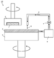
- FIG. 1 is a diagram showing an example of a polishing apparatus that can be used in the polishing method of the present invention.
- An abrasive according to the present invention is an abrasive for polishing a surface to be polished of an object to be polished, and includes first silicon oxide fine particles having an average primary particle diameter of 5 to 20 nm and an average primary particle diameter of 40 to The ratio of the first silicon oxide fine particles to the total amount of the first silicon oxide fine particles and the second silicon oxide fine particles is 0.7 to 30 and includes 110 nm second silicon oxide fine particles and water. % By mass.
- the first silicon oxide fine particles and the second silicon oxide fine particles are used as abrasive grains.
- the average primary particle diameter of the first silicon oxide fine particles and the average primary particle diameter of the second silicon oxide fine particles are set in the above ranges, respectively.
- the presence of a small amount of the first silicon oxide fine particles having a small particle size as well as the second silicon oxide fine particles having a large particle size as shown in the above blending ratio also improves the dispersion stability in a dispersion medium such as water. This contributes to the stability of long-term use.
- first silicon oxide fine particles and second silicon oxide fine particles are the same silicon oxide fine particles except that the average primary particle diameter is different.
- These can be used, and those produced by various known methods can be used.
- fumed silica obtained by vapor phase synthesis of silicon tetrachloride in an oxygen and hydrogen flame, colloidal silica obtained by ion exchange or neutralization of sodium silicate, or colloidal silica obtained by hydrolyzing silicon alkoxide in the liquid phase, etc.
- silicon oxide fine particles are examples of these, in the abrasive
- the average primary particle diameter of the first silicon oxide fine particles contained in the abrasive of the present invention is 5 to 20 nm, preferably 5 to 15 nm, and more preferably 7 to 13 nm.
- the first silicon oxide fine particles smaller than 5 nm cannot be present stably, and if the first silicon oxide fine particles exceeding 20 nm are used, there is a possibility that a preferable polishing rate cannot be obtained.
- the average primary particle diameter of the second silicon oxide fine particles contained in the abrasive of the present invention is 40 to 110 nm as described above, preferably 45 to 100 nm. If the second silicon oxide fine particles exceeding 100 nm are used, the surface accuracy of the surface to be polished may be deteriorated. If the second silicon oxide fine particles smaller than 40 nm are used, a preferable polishing rate may not be obtained. is there.
- the average primary particle diameter of the silicon oxide fine particles is a value obtained by converting a specific surface area measured by a nitrogen adsorption BET method into a diameter of a spherical particle.
- the blending ratio of the first silicon oxide fine particles and the second silicon oxide fine particles in the polishing agent of the present invention is the first occupying the total amount of the first silicon oxide fine particles and the second silicon oxide fine particles as described above.
- the blending ratio is such that the ratio of 1 silicon oxide fine particles is 0.7 to 30% by weight, and this blending ratio is preferably 1 to 10% by weight, and more preferably 3 to 10% by weight.
- the content of the first silicon oxide fine particles and the second silicon oxide fine particles in the abrasive of the present invention is the total amount of the first silicon oxide fine particles and the second silicon oxide fine particles, and is based on the total mass of the abrasive. It is preferable to appropriately set the polishing rate, uniformity, material selectivity, dispersion stability, etc. within the range of 10 to 50% by mass. When the total content of the first silicon oxide fine particles and the second silicon oxide fine particles is less than 10% by mass with respect to the total mass of the abrasive, a sufficient polishing rate may not be obtained. The improvement of the polishing rate commensurate with the increase in the abrasive grain concentration is not recognized, the viscosity of the abrasive is excessively increased, and the gelation of the abrasive may be promoted.
- the total content of the first silicon oxide fine particles and the second silicon oxide fine particles in the abrasive of the present invention is more preferably in the range of 15 to 30% by mass with respect to the total mass of the abrasive.
- the water contained in the abrasive of the present invention disperses the first silicon oxide fine particles and the second silicon oxide fine particles, which are abrasive grains, and other optional components added as necessary. It is a medium for dispersing and dissolving. Although there is no restriction
- water is preferably contained in the range of 40 to 90% by mass with respect to the total mass of the abrasive.
- the viscosity of the abrasive becomes high and the fluidity may be impaired.
- the concentration of the silicon oxide fine particles and the second silicon oxide fine particles become low, and a sufficient polishing rate cannot be obtained.
- the polishing agent of the present invention contains the first silicon oxide fine particles and the second silicon oxide fine particles of (1), which are contained as essential components, and water of (2), for example. It can be prepared by weighing and mixing so as to achieve the above blending amount.
- colloidal silica is used as both the first silicon oxide fine particles and the second silicon oxide fine particles, the colloidal silica is supplied in a state where the silicon oxide fine particles are dispersed in water in advance.
- Colloidal silica containing silicon oxide fine particles and colloidal silica containing the second silicon oxide fine particles are mixed at a desired ratio, and can be prepared as the abrasive of the present invention by simply diluting with water.
- polishing agent of this invention in the range which does not impair the effect of the said this invention, contains in addition to the essential component of said (1), (2). Such optional components may be included.
- the polishing agent of the present invention is a polishing agent for polishing the surface to be polished of the polishing object, and is not particularly limited as a polishing object. Specific examples include a glass substrate, a silicon wafer, a semiconductor device wiring substrate, and a compound single crystal substrate. Among these, the polishing agent of the present invention can increase the effect when polishing a compound single crystal substrate, and more particularly, when used for a single crystal substrate having a modified Mohs hardness of 10 or more, The effect of high-speed polishing and long-term stable use can be greatly expected.
- the single crystal substrate having the modified Mohs hardness of 10 or more include a sapphire ( ⁇ -Al 2 O 3 ) substrate (hardness: 12), a silicon carbide (SiC) substrate (hardness: 13), and gallium nitride (GaN). Examples thereof include a substrate (hardness: 13).
- polishing agent of this invention is preferably used especially for grinding
- polishing method As a method of polishing the surface to be polished of the object to be polished using the polishing agent of the present invention, the surface to be polished and the polishing pad of the object to be polished are brought into contact with each other while supplying the abrasive to the polishing pad.
- a polishing method in which polishing is performed by the relative motion is preferable.
- FIG. 1 shows an example of a polishing apparatus that circulates and uses an abrasive that can be used in an embodiment of the present invention, which will be described below.
- the polishing apparatus used in the embodiment of the present invention has such a structure. It is not limited to things.
- the polishing apparatus 10 includes a polishing head 2 that holds an object 1 to be polished, a polishing surface plate 3, a polishing pad 4 that is attached to the surface of the polishing surface plate 3, a tank 8 that stores an abrasive 5, A polishing agent supply pipe 7 for supplying the polishing agent 5 from the tank 8 to the polishing pad 4 using the polishing agent supply pump 7 is provided.
- the polishing apparatus 10 brings the polishing surface of the object 1 held by the polishing head 2 into contact with the polishing pad 4 while supplying the polishing agent 5 from the polishing agent supply pipe 6, and the polishing head 2 and the polishing surface plate 3. And are relatively rotated to perform polishing.
- the polishing apparatus 10 is a polishing apparatus that polishes one surface of an object to be polished as a surface to be polished.
- a double-sided simultaneous polishing apparatus in which polishing pads similar to the polishing apparatus 10 are disposed on the upper and lower surfaces of the object to be polished. It is also possible to polish the surface to be polished (both sides) of the object to be polished.
- the polishing head 2 may move linearly as well as rotationally. Further, the polishing surface plate 3 and the polishing pad 4 may be as large as or smaller than the polishing object 1. In that case, it is preferable that the entire surface of the object to be polished 1 can be polished by relatively moving the polishing head 2 and the polishing surface plate 3. Furthermore, the polishing surface plate 3 and the polishing pad 4 do not have to perform rotational movement, and may move in one direction, for example, by a belt type.
- the polishing conditions of the polishing apparatus 10 are not particularly limited, but by applying a load to the polishing head 2 and pressing it against the polishing pad 4, it is possible to increase the polishing pressure and improve the polishing rate.
- the polishing pressure is preferably about 10 to 50 kPa, and more preferably about 10 to 40 kPa from the viewpoint of the in-surface uniformity of the polishing object 1 at the polishing rate, flatness, and prevention of polishing defects such as scratches.
- the number of rotations of the polishing surface plate 3 and the polishing head 2 is preferably about 50 to 500 rpm, but is not limited thereto.
- the supply amount of the abrasive 5 is appropriately adjusted and selected depending on the material constituting the surface to be polished, the composition of the abrasive, the above polishing conditions, etc. For example, when polishing a wafer having a diameter of 50 mm, A supply amount of about 5 to 300 cm 3 / min is preferable.
- the polishing pad 4 may be made of a general nonwoven fabric, foamed polyurethane, porous resin, non-porous resin, or the like. Further, in order to promote the supply of the polishing agent 5 to the polishing pad 4 or to collect a certain amount of the polishing agent 5 on the polishing pad 4, the surface of the polishing pad 4 has a lattice shape, a concentric circle shape, a spiral shape, or the like. Groove processing may be performed.
- the pad conditioner may be brought into contact with the surface of the polishing pad 4 to perform polishing while conditioning the surface of the polishing pad 4.
- the polishing apparatus 10 shown in FIG. 1 has a recovery unit (not shown) for recovering the abrasive 5 used for polishing from the polishing pad 4, and the recovered abrasive 5 is transported to the tank 8. It has become.
- the abrasive 5 returned to the tank 8 is supplied to the polishing pad 4 through the abrasive supply pipe 6 again using the abrasive supply pump 7.
- the abrasive 5 is circulated and used in this way.
- the polishing agent supplied to the polishing pad is recovered in the same manner as described above after being used for polishing, but is discarded after each polishing use. Can also be used.
- a polishing method in which an abrasive is used in a circulating manner is preferable because the consumption of the abrasive can be reduced as compared with a polishing method in which the abrasive is discarded for each polishing use.
- the components to be polished are mixed into the polishing agent by polishing, so conventional polishing agents tend to cause aggregation and gelation of abrasive grains, and gradually cause clogging of the pad.
- the polishing rate decreased.
- the polishing agent of the present invention gelation and aggregation due to mixing of the abrasive component generated by the polishing are unlikely to occur, and a decrease in the polishing rate during circulation use is suppressed.
- the polishing agent of the present invention has the characteristics that the initial polishing rate is high and the decrease in the polishing rate when used in a circulation system is suppressed. This not only improves the efficiency of the polishing process, but also reduces the consumption of abrasives, shortens downtime by reducing the frequency of pad dressing and flushing, etc., and also reduces the pad consumption. Therefore, it can be said that it has great significance for improving the mass productivity of various device manufacturing.
- Examples 1 to 6 are examples, and examples 7 to 12 are comparative examples.
- Example 1 Colloidal silica having an average primary particle size of 10 nm as the first silicon oxide fine particles (an aqueous dispersion having a solid content concentration of 40% by mass of the first silicon oxide fine particles) and an average primary particle size of 80 nm as the second silicon oxide fine particles.
- the first silicon oxide fine particles occupying the total amount of the first silicon oxide fine particles and the second silicon oxide fine particles in the above colloidal silica (the aqueous dispersion of the second silicon oxide fine particles having a solid concentration of 40% by mass).
- the mixture was mixed at such a ratio that the ratio became 1% by mass and sufficiently stirred.
- the first mass with respect to the total mass of the abrasive finally obtained that is, the total mass of the total amount of the first silicon oxide fine particles and the second silicon oxide fine particles and the amount of water.
- a polishing agent was prepared by adding ion-exchanged water so that the total amount of the silicon oxide fine particles and the second silicon oxide fine particles was 20% by mass.
- the first silicon oxide fine particles and the second silicon oxide fine particles are abrasive components.
- Table 1 shows the average primary particle diameter and blending ratio of each silicon oxide fine particle with respect to the abrasive component composed of the first silicon oxide fine particle and the second silicon oxide fine particle in the abrasive obtained in Example 1 above.
- the abundance ratio of abrasive grains: water in the abrasive is 20:80 (mass ratio).
- the average primary particle diameter of the silicon oxide fine particles blended in the abrasive is a value obtained by measuring the specific surface area by the nitrogen adsorption BET method.
- the average primary particle diameters of the silicon oxide fine particles used in Examples 2 to 12 are all values obtained by measurement in the same manner.
- Example 2 to 12 In the same manner as in Example 1, the first silicon oxide fine particles and the second silicon oxide fine particles having an average primary particle size shown in Table 1 were blended as abrasive components so as to have the composition shown in Table 1, The polishing of Examples 2 to 12 was performed by adding water so that the total amount of the first silicon oxide fine particles and the second silicon oxide fine particles, that is, the blending amount of the abrasive component with respect to the total mass was 20% by mass. An agent was prepared. The silicon oxide fine particles used are all colloidal silica.
- polishing characteristics of the abrasives of Examples 1 to 12 obtained above were evaluated by the following methods. As the evaluation of the polishing characteristics, (1) evaluation of the polishing rate when the abrasive was poured and used, and (2) evaluation of the persistence of the polishing rate when the abrasive was used in circulation.
- a polishing apparatus As a polishing apparatus, a table polishing apparatus manufactured by SPEEDFAM was used. As the polishing pad, (1) K-groove (use of pouring) of single-layer IC1000 and (2) SUBA800-XY-groove (use of circulation) (both manufactured by Nita Haas) were used, and MEC100-PH3. Conditioning was performed using 5L (Mitsubishi Materials Co., Ltd.) and a brush.
- the supply rate of the abrasive is (1) 10 cm 3 / min (using flowing), (2) 100 cm 3 / min (using circulation), the rotation speed of the polishing platen is 100 rpm, and the polishing pressure is 5 psi, ie 34
- the polishing time was 0.5 kPa, and the polishing time was (1) 30 minutes (use of pouring) and (2) 60 minutes (use of circulation).
- the sapphire substrate was replaced every 60 minutes, and polishing was performed continuously without any pad conditioning.
- the polishing rate was evaluated by the amount of change in the thickness of the substrate per unit time ( ⁇ m / hr). Specifically, for the single crystal sapphire substrate used in the evaluations of (1) and (2) above, the mass of an unpolished substrate with a known thickness and the substrate mass after polishing each time are measured, and the difference The change in mass was determined, and the change per hour in the thickness of the substrate determined from the change in mass was calculated using the following formula.
- the polishing rate under flowing (non-circulating) polishing agent conditions was measured and calculated as the initial polishing rate in accordance with the polishing method (1).
- the initial polishing rate was determined by determining the ratio when the initial polishing rate of the polishing agent using only the second silicon oxide fine particles having an average primary particle diameter of 80 nm prepared in Example 7 as abrasive grains was set to 1.00. did. The results are shown in Table 1.
- the polishing method was a method according to the above (2).
- the durability of the abrasive during circulation is determined by polishing until the polishing rate measured and calculated every 60 minutes is 15% lower than the initial polishing rate (the polishing rate for 60 minutes from the start of polishing).
- the cumulative polishing amount of the sapphire substrate was evaluated.
- the cumulative polishing amount of the abrasive of Example 7 was set to 1.00, and the ratio was represented by the ratio. A numerical value greater than 1.00 indicates that the polishing rate is more maintainable than the abrasive of Example 7.
- a gel is a type of dispersion system, which is a colloid of a liquid dispersion medium such as a sol, but has a high viscosity due to the dispersoid network and loses fluidity. Unlike the sol, the entire system is in a solid state. The state that became.
- the abrasive containing the first silicon oxide fine particles and the second silicon oxide fine particles having the particle diameters of the present invention in the blending ratio of the present invention is larger than the abrasive of the comparative example.
- the polishing rate is large, and the polishing rate during use is good, that is, excellent in long-term use stability.
- an object to be polished particularly a single crystal substrate having a high hardness such as a sapphire ( ⁇ -Al 2 O 3 ) substrate, a silicon carbide (SiC) substrate, a gallium nitride (GaN) substrate, or the like.
- the polishing surface can be polished at a high speed, and the long-term use stability of the abrasive can be improved. Thereby, it can contribute to the improvement of the productivity of these board
Landscapes
- Engineering & Computer Science (AREA)
- Chemical & Material Sciences (AREA)
- Mechanical Engineering (AREA)
- Materials Engineering (AREA)
- Organic Chemistry (AREA)
- Mechanical Treatment Of Semiconductor (AREA)
- Finish Polishing, Edge Sharpening, And Grinding By Specific Grinding Devices (AREA)
- Grinding-Machine Dressing And Accessory Apparatuses (AREA)
Abstract
Description
[2]前記第1の酸化ケイ素微粒子および前記第2の酸化ケイ素微粒子が、ともにコロイダルシリカである前記[1]に記載の研磨剤。
[3]前記第1の酸化ケイ素微粒子と第2の酸化ケイ素微粒子の合計量に占める前記第1の酸化ケイ素微粒子の割合が1~10質量%である前記[1]または[2]に記載の研磨剤。
[4]前記第2の酸化ケイ素微粒子の平均一次粒子径が45~100nmである前記[1]~[3]のいずれか一項に記載の研磨剤。
[5]前記第1の酸化ケイ素微粒子の平均一次粒子径が5~15nmである前記[1]~[4]のいずれか一項に記載の研磨剤。
[6]前記研磨対象物が、修正モース硬度で表わされる硬度が10以上の単結晶基板である前記[1]~[5]のいずれか一項に記載の研磨剤。
[7][1]~[6]のいずれか一項に記載の研磨剤を研磨パッドに供給し、研磨対象物の被研磨面と前記研磨パッドとを接触させて、両者間の相対運動により研磨する研磨方法。
[8]前記研磨パッドに供給され研磨に使用された研磨剤を回収し、前記回収した研磨剤を再び研磨パッドに供給する操作を繰り返し行うことで前記研磨剤を循環使用する前記[7]記載の研磨方法。
本発明に係る研磨剤は、研磨対象物の被研磨面を研磨するための研磨剤であって、平均一次粒子径が5~20nmの第1の酸化ケイ素微粒子と、平均一次粒子径が40~110nmの第2の酸化ケイ素微粒子と、水とを含み、かつ前記第1の酸化ケイ素微粒子と第2の酸化ケイ素微粒子の合計量に占める前記第1の酸化ケイ素微粒子の割合が0.7~30質量%である。
本発明の研磨剤において、第1の酸化ケイ素微粒子および第2の酸化ケイ素微粒子は平均一次粒子径が異なる以外は同様の酸化ケイ素微粒子を用いることが可能であり、ともに種々の公知の方法で製造されるものを使用できる。例えば、四塩化ケイ素を酸素と水素の火炎中で気相合成したヒュームドシリカやケイ酸ナトリウムをイオン交換、もしくは中和後脱塩したコロイダルシリカまたはケイ素アルコキシドを液相で加水分解したコロイダルシリカ等の酸化ケイ素微粒子が挙げられる。これらのうちでも、本発明の研磨剤においては、品種の多様性の観点からケイ酸ナトリウムを出発原料とするコロイダルシリカがより好ましい。
5nmより小さい第1の酸化ケイ素微粒子は、安定に存在出来ないおそれがあり、また20nmを超える第1の酸化ケイ素微粒子を用いると好ましい研磨速度を得られない可能性がある。
本発明の研磨剤が含有する水は、研磨砥粒である上記第1の酸化ケイ素微粒子および第2の酸化ケイ素微粒子を分散させるとともに、その他必要に応じて添加される任意成分を分散・溶解するための媒体である。水については、特に制限はないが、他の配合成分に対する影響、不純物の混入、pH等への影響から、純水または脱イオン水が好ましい。水は研磨剤の流動性を制御する機能を有するので、その含有量は、研磨速度、平坦化特性等の目標とする研磨特性に合わせて適宜設定することができる。
本発明の研磨剤は、必須成分として含有する上記(1)の第1の酸化ケイ素微粒子および第2の酸化ケイ素微粒子と、(2)の水を、例えば、上記配合量となるように秤量し、混合することにより調製できる。
ここで、上記第1の酸化ケイ素微粒子および第2の酸化ケイ素微粒子として、ともにコロイダルシリカを用いた場合、コロイダルシリカはあらかじめ酸化ケイ素微粒子が水に分散した状態で供給されるため、上記第1の酸化ケイ素微粒子を含むコロイダルシリカと、上記第2の酸化ケイ素微粒子を含むコロイダルシリカを所望の割合で混合し、適宜水によって希釈するだけで本発明の研磨剤として調製できる。
本発明の研磨剤は、研磨対象物の被研磨面を研磨するための研磨剤であり、研磨対象物としては特に制限されない。具体的には、ガラス基板、シリコンウェハ、半導体デバイス配線基板、化合物単結晶基板等が挙げられる。これらのうちでも本発明の研磨剤は、化合物単結晶基板を研磨する際により大きな効果を上げることが可能であり、特に、修正モース硬度による硬度が10以上の単結晶基板に用いることで、より高速研磨、長時間安定使用の効果が大きく期待できる。
本発明の研磨剤を用いて、研磨対象物の被研磨面を研磨する方法としては、研磨剤を研磨パッドに供給しながら、研磨対象物の被研磨面と研磨パッドとを接触させ、両者間の相対運動により研磨を行う研磨方法が好ましい。
第1の酸化ケイ素微粒子として平均一次粒子径が10nmのコロイダルシリカ(第1の酸化ケイ素微粒子の固形分濃度40質量%の水分散液)と、第2の酸化ケイ素微粒子として平均一次粒子径が80nmのコロイダルシリカ(第2の酸化ケイ素微粒子の固形分濃度40質量%の水分散液)を、第1の酸化ケイ素微粒子と第2の酸化ケイ素微粒子の合計量に占める第1の酸化ケイ素微粒子の配合割合が1質量%となるような割合で混合し、充分に撹拌した。得られた混合液に、最終的に得られる研磨剤の全質量、すなわち、第1の酸化ケイ素微粒子と第2の酸化ケイ素微粒子の合計量と水の量との合計質量、に対する、第1の酸化ケイ素微粒子と第2の酸化ケイ素微粒子の合計量が、20質量%となるように、イオン交換水を添加して研磨剤を調製した。得られた研磨剤においては、第1の酸化ケイ素微粒子および第2の酸化ケイ素微粒子が砥粒成分である。
なお、研磨剤に配合した酸化ケイ素微粒子の平均一次粒子径は、窒素吸着BET法により比表面積を測定して得られた値である。以下、例2~12に用いた酸化ケイ素微粒子の平均一次粒子径は全て同様の方法で測定して得られた値である。
例1と同様にして表1に示す平均一次粒子径の第1の酸化ケイ素微粒子と第2の酸化ケイ素微粒子とを砥粒成分として表1に示す組成となるように配合し、さらに研磨剤の全質量に対する、第1の酸化ケイ素微粒子と第2の酸化ケイ素微粒子の合計量、すなわち砥粒成分の配合量が、20質量%となるように水を添加して、例2~例12の研磨剤を調製した。なお、用いた酸化ケイ素微粒子は全てコロイダルシリカである。
上記で得られた例1~例12の研磨剤の研磨特性を以下の方法により評価した。
研磨特性の評価としては、(1)研磨剤を掛け流し使用した際の研磨速度の評価、(2)研磨剤を循環使用した際の研磨速度の持続性の評価を行った。
(1)、(2)の評価ともに、被研磨物として、単結晶サファイア基板の2インチウェハ(信光社製、(0001)面、基板の厚み420μm)を使用した。
研磨装置としては、SPEEDFAM社製卓上研磨装置を使用した。研磨パッドとしては、(1)単層IC1000のK-groove(掛け流し使用)および(2)SUBA800-XY-groove(循環使用)(ともにニッタハース社製)を使用し、試験前にMEC100-PH3.5L(三菱マテリアル社製)および、ブラシを用いてコンディショニングを行った。
研磨速度は、単位時間当たりの基板の厚さの変化量(μm/hr)で評価した。具体的には、上記(1)、(2)の評価に用いた単結晶サファイア基板について、厚みが既知の未研磨基板の質量と各時間研磨した後の基板質量とを測定し、その差から質量変化を求め、更に質量変化から求めた基板の厚みの時間当たりの変化を下記の式を用いて算出した。
Δm=m0-m1
V=Δm/m0 × T0 × 60/t
(式中、Δm(g)は研磨前後の質量変化、m0(g)は未研磨基板の初期質量、m1(g)は研磨後基板の質量、Vは研磨速度(μm/hr)、T0は未研磨基板の基板厚み(μm)、tは研磨時間(min)を表す。)
まず、例1~例12の研磨剤について、前記研磨方法(1)に則り、掛け流し(非循環使用)研磨剤条件での研磨速度を初期研磨速度として測定・算出した。なお、初期研磨速度は、例7で調製した平均一次粒子径が80nmの第2の酸化ケイ素微粒子のみを砥粒とした研磨剤の初期研磨速度を1.00としたときの比率を求めて表した。結果を表1に示す。

次に研磨剤を循環して使用したときの研磨速度の持続性について以下の方法で評価した。研磨方法は前記(2)に則った方法であった。循環使用時の研磨剤の持続性は、60分間毎に測定・算出した研磨速度が、初期の研磨速度(研磨開始から60分間の研磨速度)に比べて15%低下するまで研磨を行った際のサファイア基板の累積研磨量で評価した。例7の研磨剤の累積研磨量を1.00として、その比率によって表した。数値が1.00より大きければ、例7の研磨剤より研磨速度の維持性がよいことを示している。
ここで、ゲルとは分散系の一種で、ゾルのような液体分散媒のコロイドであるが、分散質のネットワークにより高い粘性を持ち流動性を失い、ゾルとは異なり、系全体としては固体状になった状態をいう。

本出願は、2010年7月9日出願の日本特許出願2010-156536に基づくものであり、その内容はここに参照として取り込まれる。
Claims (8)
- 研磨対象物の被研磨面を研磨するための研磨剤であって、平均一次粒子径が5~20nmの第1の酸化ケイ素微粒子と、平均一次粒子径が40~110nmの第2の酸化ケイ素微粒子と、水とを含み、かつ前記第1の酸化ケイ素微粒子と第2の酸化ケイ素微粒子の合計量に占める前記第1の酸化ケイ素微粒子の割合が0.7~30質量%である研磨剤。
- 前記第1の酸化ケイ素微粒子および前記第2の酸化ケイ素微粒子が、ともにコロイダルシリカである請求項1に記載の研磨剤。
- 前記第1の酸化ケイ素微粒子と第2の酸化ケイ素微粒子の合計量に占める前記第1の酸化ケイ素微粒子の割合が1~10質量%である請求項1または2に記載の研磨剤。
- 前記第2の酸化ケイ素微粒子の平均一次粒子径が45~100nmである請求項1~3のいずれか一項に記載の研磨剤。
- 前記第1の酸化ケイ素微粒子の平均一次粒子径が5~15nmである請求項1~4のいずれか一項に記載の研磨剤。
- 前記研磨対象物が、修正モース硬度で表わされる硬度が10以上の単結晶基板である請求項1~5のいずれか一項に記載の研磨剤。
- 請求項1~6のいずれか一項に記載の研磨剤を研磨パッドに供給し、研磨対象物の被研磨面と前記研磨パッドとを接触させて、両者間の相対運動により研磨する研磨方法。
- 前記研磨パッドに供給され研磨に使用された研磨剤を回収し、前記回収した研磨剤を再び研磨パッドに供給する操作を繰り返し行うことで前記研磨剤を循環使用する請求項7記載の研磨方法。
Priority Applications (4)
| Application Number | Priority Date | Filing Date | Title |
|---|---|---|---|
| JP2012523826A JPWO2012005142A1 (ja) | 2010-07-09 | 2011-06-28 | 研磨剤および研磨方法 |
| KR1020137000480A KR20130114635A (ko) | 2010-07-09 | 2011-06-28 | 연마제 및 연마 방법 |
| CN201180033927XA CN102985508A (zh) | 2010-07-09 | 2011-06-28 | 研磨剂和研磨方法 |
| US13/737,210 US20130130595A1 (en) | 2010-07-09 | 2013-01-09 | Polishing agent and polishing method |
Applications Claiming Priority (2)
| Application Number | Priority Date | Filing Date | Title |
|---|---|---|---|
| JP2010-156536 | 2010-07-09 | ||
| JP2010156536 | 2010-07-09 |
Related Child Applications (1)
| Application Number | Title | Priority Date | Filing Date |
|---|---|---|---|
| US13/737,210 Continuation US20130130595A1 (en) | 2010-07-09 | 2013-01-09 | Polishing agent and polishing method |
Publications (1)
| Publication Number | Publication Date |
|---|---|
| WO2012005142A1 true WO2012005142A1 (ja) | 2012-01-12 |
Family
ID=45441125
Family Applications (1)
| Application Number | Title | Priority Date | Filing Date |
|---|---|---|---|
| PCT/JP2011/064786 Ceased WO2012005142A1 (ja) | 2010-07-09 | 2011-06-28 | 研磨剤および研磨方法 |
Country Status (6)
| Country | Link |
|---|---|
| US (1) | US20130130595A1 (ja) |
| JP (1) | JPWO2012005142A1 (ja) |
| KR (1) | KR20130114635A (ja) |
| CN (1) | CN102985508A (ja) |
| TW (1) | TW201213472A (ja) |
| WO (1) | WO2012005142A1 (ja) |
Cited By (4)
| Publication number | Priority date | Publication date | Assignee | Title |
|---|---|---|---|---|
| JP2013201176A (ja) * | 2012-03-23 | 2013-10-03 | Mitsubishi Chemicals Corp | ポリシングスラリー、及び第13族窒化物基板の製造方法 |
| KR20150065682A (ko) * | 2012-08-24 | 2015-06-15 | 에코랍 유에스에이 인코퍼레이티드 | 사파이어 표면 폴리싱 방법 |
| JP2016520436A (ja) * | 2013-03-15 | 2016-07-14 | エコラボ ユーエスエー インコーポレイティド | サファイアの表面を研磨する方法 |
| CN106737130A (zh) * | 2016-12-30 | 2017-05-31 | 苏州爱彼光电材料有限公司 | 蓝宝石基板研磨装置 |
Families Citing this family (9)
| Publication number | Priority date | Publication date | Assignee | Title |
|---|---|---|---|---|
| JP6156207B2 (ja) * | 2013-04-02 | 2017-07-05 | 信越化学工業株式会社 | 合成石英ガラス基板の製造方法 |
| JP2016155900A (ja) * | 2015-02-23 | 2016-09-01 | 株式会社フジミインコーポレーテッド | 研磨用組成物、研磨方法及び硬脆材料基板の製造方法 |
| CN104893587A (zh) * | 2015-03-09 | 2015-09-09 | 江苏中晶科技有限公司 | 高效c向蓝宝石抛光液及其制备方法 |
| CN104924195A (zh) * | 2015-06-12 | 2015-09-23 | 浙江工业大学 | 一种蓝宝石晶片高效超精密加工方法 |
| CN107052990A (zh) * | 2016-12-01 | 2017-08-18 | 苏州爱彼光电材料有限公司 | 蓝宝石基板研磨装置 |
| US10377014B2 (en) | 2017-02-28 | 2019-08-13 | Ecolab Usa Inc. | Increased wetting of colloidal silica as a polishing slurry |
| CN108081147A (zh) * | 2017-12-15 | 2018-05-29 | 德淮半导体有限公司 | 晶圆研磨装置及废液排放管路 |
| CN108789163A (zh) * | 2018-05-30 | 2018-11-13 | 郑州合晶硅材料有限公司 | 一种硅片背面抛光用装置及抛光方法 |
| US12285844B2 (en) | 2018-06-15 | 2025-04-29 | Mirka Ltd | Abrading with an abrading plate |
Citations (6)
| Publication number | Priority date | Publication date | Assignee | Title |
|---|---|---|---|---|
| JP2008131001A (ja) * | 2006-11-24 | 2008-06-05 | Nichia Chem Ind Ltd | 半導体発光素子及び半導体発光素子の製造方法 |
| JP2008163054A (ja) * | 2006-12-26 | 2008-07-17 | Kao Corp | 容器入り分散液 |
| JP2008192656A (ja) * | 2007-01-31 | 2008-08-21 | Nitta Haas Inc | 研磨組成物用添加剤 |
| JP4253141B2 (ja) * | 2000-08-21 | 2009-04-08 | 株式会社東芝 | 化学機械研磨用スラリおよび半導体装置の製造方法 |
| JP2009238891A (ja) * | 2008-03-26 | 2009-10-15 | Hitachi Metals Ltd | SiC単結晶基板の製造方法 |
| JP2010042509A (ja) * | 2000-05-12 | 2010-02-25 | Nissan Chem Ind Ltd | 研磨用組成物 |
Family Cites Families (4)
| Publication number | Priority date | Publication date | Assignee | Title |
|---|---|---|---|---|
| JPH04253141A (ja) * | 1991-01-28 | 1992-09-08 | Nec Kagoshima Ltd | 表示管 |
| JPH11256141A (ja) * | 1998-03-12 | 1999-09-21 | Sony Corp | 研磨スラリーおよび研磨方法 |
| US20020104269A1 (en) * | 2001-01-26 | 2002-08-08 | Applied Materials, Inc. | Photochemically enhanced chemical polish |
| JP4959763B2 (ja) * | 2009-08-28 | 2012-06-27 | 昭和電工株式会社 | SiCエピタキシャルウェハ及びその製造方法 |
-
2011
- 2011-06-28 CN CN201180033927XA patent/CN102985508A/zh active Pending
- 2011-06-28 KR KR1020137000480A patent/KR20130114635A/ko not_active Withdrawn
- 2011-06-28 WO PCT/JP2011/064786 patent/WO2012005142A1/ja not_active Ceased
- 2011-06-28 JP JP2012523826A patent/JPWO2012005142A1/ja not_active Withdrawn
- 2011-07-08 TW TW100124303A patent/TW201213472A/zh unknown
-
2013
- 2013-01-09 US US13/737,210 patent/US20130130595A1/en not_active Abandoned
Patent Citations (6)
| Publication number | Priority date | Publication date | Assignee | Title |
|---|---|---|---|---|
| JP2010042509A (ja) * | 2000-05-12 | 2010-02-25 | Nissan Chem Ind Ltd | 研磨用組成物 |
| JP4253141B2 (ja) * | 2000-08-21 | 2009-04-08 | 株式会社東芝 | 化学機械研磨用スラリおよび半導体装置の製造方法 |
| JP2008131001A (ja) * | 2006-11-24 | 2008-06-05 | Nichia Chem Ind Ltd | 半導体発光素子及び半導体発光素子の製造方法 |
| JP2008163054A (ja) * | 2006-12-26 | 2008-07-17 | Kao Corp | 容器入り分散液 |
| JP2008192656A (ja) * | 2007-01-31 | 2008-08-21 | Nitta Haas Inc | 研磨組成物用添加剤 |
| JP2009238891A (ja) * | 2008-03-26 | 2009-10-15 | Hitachi Metals Ltd | SiC単結晶基板の製造方法 |
Cited By (8)
| Publication number | Priority date | Publication date | Assignee | Title |
|---|---|---|---|---|
| JP2013201176A (ja) * | 2012-03-23 | 2013-10-03 | Mitsubishi Chemicals Corp | ポリシングスラリー、及び第13族窒化物基板の製造方法 |
| KR20150065682A (ko) * | 2012-08-24 | 2015-06-15 | 에코랍 유에스에이 인코퍼레이티드 | 사파이어 표면 폴리싱 방법 |
| JP2015533868A (ja) * | 2012-08-24 | 2015-11-26 | エコラブ ユーエスエイ インク | サファイア表面を研磨する方法 |
| EP2888077A4 (en) * | 2012-08-24 | 2016-06-08 | Ecolab Usa Inc | METHOD FOR POLISHING SURFACES FROM SAPHIR |
| KR102105844B1 (ko) | 2012-08-24 | 2020-04-29 | 에코랍 유에스에이 인코퍼레이티드 | 사파이어 표면 폴리싱 방법 |
| JP2016520436A (ja) * | 2013-03-15 | 2016-07-14 | エコラボ ユーエスエー インコーポレイティド | サファイアの表面を研磨する方法 |
| US9896604B2 (en) | 2013-03-15 | 2018-02-20 | Ecolab Usa Inc. | Methods of polishing sapphire surfaces |
| CN106737130A (zh) * | 2016-12-30 | 2017-05-31 | 苏州爱彼光电材料有限公司 | 蓝宝石基板研磨装置 |
Also Published As
| Publication number | Publication date |
|---|---|
| JPWO2012005142A1 (ja) | 2013-09-02 |
| CN102985508A (zh) | 2013-03-20 |
| TW201213472A (en) | 2012-04-01 |
| US20130130595A1 (en) | 2013-05-23 |
| KR20130114635A (ko) | 2013-10-18 |
Similar Documents
| Publication | Publication Date | Title |
|---|---|---|
| JPWO2012005142A1 (ja) | 研磨剤および研磨方法 | |
| CN101512732B (zh) | 利用水溶性氧化剂的碳化硅抛光方法 | |
| EP2365042B1 (en) | Polishing composition and polishing method using the same | |
| JP5614498B2 (ja) | 非酸化物単結晶基板の研磨方法 | |
| JP5418590B2 (ja) | 研磨剤、研磨剤セット及び基板の研磨方法 | |
| EP3470487B1 (en) | Mixed abrasive polishing compositions | |
| CN101535431B (zh) | 一种用于抛光多晶硅的化学机械抛光液 | |
| WO2012165376A1 (ja) | 研磨剤および研磨方法 | |
| WO2019181013A1 (ja) | 研磨液、研磨液セット及び研磨方法 | |
| CN1667026B (zh) | 抛光浆料及其制备方法和基板的抛光方法 | |
| CN102017093A (zh) | 使用水溶性氧化剂的碳化硅抛光方法 | |
| WO2013035539A1 (ja) | 研磨剤および研磨方法 | |
| CN104745092A (zh) | 一种应用于sti领域的化学机械抛光液及其使用方法 | |
| JP6581299B2 (ja) | Cmp用スラリー組成物及びこれを用いた研磨方法 | |
| JP2012248569A (ja) | 研磨剤および研磨方法 | |
| JP5516594B2 (ja) | Cmp研磨液、並びに、これを用いた研磨方法及び半導体基板の製造方法 | |
| JP2004165424A (ja) | 研磨剤組成物とそれによる研磨方法 | |
| JP2014216368A (ja) | 研磨剤および研磨方法 | |
| US20040127045A1 (en) | Chemical mechanical planarization of wafers or films using fixed polishing pads and a nanoparticle composition | |
| CN1944496B (zh) | 抛光浆料及其制备方法和基板的抛光方法 | |
| JP2011161570A (ja) | 研磨剤および研磨方法 | |
| JP2014216369A (ja) | 研磨剤および研磨方法 | |
| JP4396963B2 (ja) | 研磨用組成物、その調製方法及びそれを用いたウェーハの研磨方法 | |
| KR102533083B1 (ko) | 다결정실리콘을 함유하는 웨이퍼의 연마 슬러리 조성물 | |
| JP2014204064A (ja) | 研磨剤および研磨方法 |
Legal Events
| Date | Code | Title | Description |
|---|---|---|---|
| WWE | Wipo information: entry into national phase |
Ref document number: 201180033927.X Country of ref document: CN |
|
| 121 | Ep: the epo has been informed by wipo that ep was designated in this application |
Ref document number: 11803477 Country of ref document: EP Kind code of ref document: A1 |
|
| WWE | Wipo information: entry into national phase |
Ref document number: 2012523826 Country of ref document: JP |
|
| ENP | Entry into the national phase |
Ref document number: 20137000480 Country of ref document: KR Kind code of ref document: A |
|
| NENP | Non-entry into the national phase |
Ref country code: DE |
|
| 122 | Ep: pct application non-entry in european phase |
Ref document number: 11803477 Country of ref document: EP Kind code of ref document: A1 |