WO2011152091A1 - 電極箔および有機デバイス - Google Patents
電極箔および有機デバイス Download PDFInfo
- Publication number
- WO2011152091A1 WO2011152091A1 PCT/JP2011/054627 JP2011054627W WO2011152091A1 WO 2011152091 A1 WO2011152091 A1 WO 2011152091A1 JP 2011054627 W JP2011054627 W JP 2011054627W WO 2011152091 A1 WO2011152091 A1 WO 2011152091A1
- Authority
- WO
- WIPO (PCT)
- Prior art keywords
- organic
- layer
- electrode foil
- film
- electrode
- Prior art date
- Legal status (The legal status is an assumption and is not a legal conclusion. Google has not performed a legal analysis and makes no representation as to the accuracy of the status listed.)
- Ceased
Links
Images


Classifications
-
- H—ELECTRICITY
- H01—ELECTRIC ELEMENTS
- H01B—CABLES; CONDUCTORS; INSULATORS; SELECTION OF MATERIALS FOR THEIR CONDUCTIVE, INSULATING OR DIELECTRIC PROPERTIES
- H01B1/00—Conductors or conductive bodies characterised by the conductive materials; Selection of materials as conductors
- H01B1/02—Conductors or conductive bodies characterised by the conductive materials; Selection of materials as conductors mainly consisting of metals or alloys
- H01B1/026—Alloys based on copper
-
- H—ELECTRICITY
- H05—ELECTRIC TECHNIQUES NOT OTHERWISE PROVIDED FOR
- H05B—ELECTRIC HEATING; ELECTRIC LIGHT SOURCES NOT OTHERWISE PROVIDED FOR; CIRCUIT ARRANGEMENTS FOR ELECTRIC LIGHT SOURCES, IN GENERAL
- H05B33/00—Electroluminescent light sources
- H05B33/12—Light sources with substantially two-dimensional [2D] radiating surfaces
- H05B33/26—Light sources with substantially two-dimensional [2D] radiating surfaces characterised by the composition or arrangement of the conductive material used as an electrode
-
- H—ELECTRICITY
- H10—SEMICONDUCTOR DEVICES; ELECTRIC SOLID-STATE DEVICES NOT OTHERWISE PROVIDED FOR
- H10K—ORGANIC ELECTRIC SOLID-STATE DEVICES
- H10K30/00—Organic devices sensitive to infrared radiation, light, electromagnetic radiation of shorter wavelength or corpuscular radiation
- H10K30/80—Constructional details
- H10K30/81—Electrodes
-
- H—ELECTRICITY
- H10—SEMICONDUCTOR DEVICES; ELECTRIC SOLID-STATE DEVICES NOT OTHERWISE PROVIDED FOR
- H10K—ORGANIC ELECTRIC SOLID-STATE DEVICES
- H10K50/00—Organic light-emitting devices
- H10K50/80—Constructional details
- H10K50/805—Electrodes
- H10K50/81—Anodes
- H10K50/818—Reflective anodes, e.g. ITO combined with thick metallic layers
-
- H—ELECTRICITY
- H10—SEMICONDUCTOR DEVICES; ELECTRIC SOLID-STATE DEVICES NOT OTHERWISE PROVIDED FOR
- H10K—ORGANIC ELECTRIC SOLID-STATE DEVICES
- H10K50/00—Organic light-emitting devices
- H10K50/80—Constructional details
- H10K50/805—Electrodes
- H10K50/82—Cathodes
- H10K50/826—Multilayers, e.g. opaque multilayers
-
- H—ELECTRICITY
- H10—SEMICONDUCTOR DEVICES; ELECTRIC SOLID-STATE DEVICES NOT OTHERWISE PROVIDED FOR
- H10K—ORGANIC ELECTRIC SOLID-STATE DEVICES
- H10K50/00—Organic light-emitting devices
- H10K50/80—Constructional details
- H10K50/87—Arrangements for heating or cooling
-
- H—ELECTRICITY
- H10—SEMICONDUCTOR DEVICES; ELECTRIC SOLID-STATE DEVICES NOT OTHERWISE PROVIDED FOR
- H10K—ORGANIC ELECTRIC SOLID-STATE DEVICES
- H10K65/00—Integrated devices, or assemblies of multiple devices, comprising at least one organic light-emitting element and at least one organic radiation-sensitive element, e.g. organic opto-couplers
-
- H—ELECTRICITY
- H10—SEMICONDUCTOR DEVICES; ELECTRIC SOLID-STATE DEVICES NOT OTHERWISE PROVIDED FOR
- H10K—ORGANIC ELECTRIC SOLID-STATE DEVICES
- H10K39/00—Integrated devices, or assemblies of multiple devices, comprising at least one organic radiation-sensitive element covered by group H10K30/00
- H10K39/10—Organic photovoltaic [PV] modules; Arrays of single organic PV cells
-
- Y—GENERAL TAGGING OF NEW TECHNOLOGICAL DEVELOPMENTS; GENERAL TAGGING OF CROSS-SECTIONAL TECHNOLOGIES SPANNING OVER SEVERAL SECTIONS OF THE IPC; TECHNICAL SUBJECTS COVERED BY FORMER USPC CROSS-REFERENCE ART COLLECTIONS [XRACs] AND DIGESTS
- Y02—TECHNOLOGIES OR APPLICATIONS FOR MITIGATION OR ADAPTATION AGAINST CLIMATE CHANGE
- Y02E—REDUCTION OF GREENHOUSE GAS [GHG] EMISSIONS, RELATED TO ENERGY GENERATION, TRANSMISSION OR DISTRIBUTION
- Y02E10/00—Energy generation through renewable energy sources
- Y02E10/50—Photovoltaic [PV] energy
- Y02E10/549—Organic PV cells
-
- Y—GENERAL TAGGING OF NEW TECHNOLOGICAL DEVELOPMENTS; GENERAL TAGGING OF CROSS-SECTIONAL TECHNOLOGIES SPANNING OVER SEVERAL SECTIONS OF THE IPC; TECHNICAL SUBJECTS COVERED BY FORMER USPC CROSS-REFERENCE ART COLLECTIONS [XRACs] AND DIGESTS
- Y02—TECHNOLOGIES OR APPLICATIONS FOR MITIGATION OR ADAPTATION AGAINST CLIMATE CHANGE
- Y02P—CLIMATE CHANGE MITIGATION TECHNOLOGIES IN THE PRODUCTION OR PROCESSING OF GOODS
- Y02P70/00—Climate change mitigation technologies in the production process for final industrial or consumer products
- Y02P70/50—Manufacturing or production processes characterised by the final manufactured product
-
- Y—GENERAL TAGGING OF NEW TECHNOLOGICAL DEVELOPMENTS; GENERAL TAGGING OF CROSS-SECTIONAL TECHNOLOGIES SPANNING OVER SEVERAL SECTIONS OF THE IPC; TECHNICAL SUBJECTS COVERED BY FORMER USPC CROSS-REFERENCE ART COLLECTIONS [XRACs] AND DIGESTS
- Y10—TECHNICAL SUBJECTS COVERED BY FORMER USPC
- Y10T—TECHNICAL SUBJECTS COVERED BY FORMER US CLASSIFICATION
- Y10T428/00—Stock material or miscellaneous articles
- Y10T428/12—All metal or with adjacent metals
- Y10T428/12431—Foil or filament smaller than 6 mils
- Y10T428/12438—Composite
-
- Y—GENERAL TAGGING OF NEW TECHNOLOGICAL DEVELOPMENTS; GENERAL TAGGING OF CROSS-SECTIONAL TECHNOLOGIES SPANNING OVER SEVERAL SECTIONS OF THE IPC; TECHNICAL SUBJECTS COVERED BY FORMER USPC CROSS-REFERENCE ART COLLECTIONS [XRACs] AND DIGESTS
- Y10—TECHNICAL SUBJECTS COVERED BY FORMER USPC
- Y10T—TECHNICAL SUBJECTS COVERED BY FORMER US CLASSIFICATION
- Y10T428/00—Stock material or miscellaneous articles
- Y10T428/12—All metal or with adjacent metals
- Y10T428/12493—Composite; i.e., plural, adjacent, spatially distinct metal components [e.g., layers, joint, etc.]
- Y10T428/12986—Adjacent functionally defined components
Definitions
- the present invention relates to an electrode foil using a metal foil, and an organic device such as an organic EL element, an organic EL lighting, and an organic solar battery using the electrode foil.
- organic EL lighting has attracted attention as an environmentally friendly green device.
- Features of organic EL lighting include 1) low power consumption compared to incandescent lamps, 2) thin and lightweight, and 3) flexibility.
- organic EL lighting is being developed to realize the features 2) and 3). In this respect, it is impossible to realize the features 2) and 3) above with a glass substrate that has been conventionally used in a flat panel display (FPD) or the like.
- FPD flat panel display
- Ultra-thin glass is excellent in heat resistance, barrier properties, and light transmission properties, and also has good flexibility, but handling properties are slightly inferior, thermal conductivity is low, and material cost is high.
- the resin film is excellent in handling properties and flexibility, has a low material cost, and has good light transmittance, but has poor heat resistance and barrier properties, and has low thermal conductivity.
- the metal foil has excellent characteristics such as excellent heat resistance, barrier properties, handling properties, thermal conductivity, good flexibility, and low material cost, except that it has no light transmittance.
- the thermal conductivity of a typical flexible glass or film is as low as 1 W / m ° C. or less, whereas in the case of a copper foil, it is as high as about 280 W / m ° C.
- Patent Document 1 discloses an organic light-emitting device including a lower electrode layer, an organic layer, and an upper electrode layer on a flexible substrate.
- a metal foil that may be covered with an insulating layer is disclosed. It is described that it can be used.
- Patent Document 2 discloses a flexible insulating metal foil for an electronic device provided with a stainless steel foil having a surface roughness Ra of 30 nm to 500 nm. This metal foil is used as a support base material for forming an electronic device such as a thin film transistor (TFT) by covering the surface with an insulating film.
- TFT thin film transistor
- Patent Document 3 discloses a flexible metal foil laminate in which a thermocompression bonding polyimide coating is laminated on a metal foil surface having a surface roughness Ra of about 0.2 ⁇ m or less.
- Patent Document 4 discloses an electrolytic copper foil in which the surface roughness (Rzjis) on the deposition surface side is less than 1.0 ⁇ m in order to reduce the profile of the bonding surface with the insulating layer constituent material.
- the surface roughness (Rzjis) disclosed in the literature is at most 0.27 ⁇ m at the most flat.
- the present inventor has recently obtained an electrode foil useful for a flexible electronic device having a function as a supporting base material and a reflecting electrode and having excellent thermal conductivity by providing the reflecting layer directly on the metal foil. The knowledge that it will be.
- an object of the present invention is to provide an electrode foil useful for a flexible electronic device that has a function as a support base and a reflective electrode and is excellent in thermal conductivity.
- an electrode foil comprising a metal foil and a reflective layer provided directly on the metal foil.
- the electrode foil An organic semiconductor layer comprising an organic EL layer and / or an organic solar cell active layer directly provided on the outermost surface of the electrode foil on the reflective layer side; A transparent or translucent counter electrode provided on the organic semiconductor layer; An organic device that is an organic EL element and / or an organic solar cell is provided.
- organic EL illumination comprising the organic device as an organic EL element.
- FIG. 10 is a diagram illustrating voltage dependency characteristics of luminance measured in Example 5. It is a schematic cross section which shows another example of the electrode foil by this invention.
- 7 is a photomicrograph of a cross section of a reflective layer of an electrode foil produced in Example 6 observed with a TEM.
- 7 is a spectrum obtained by EDX analysis of an interface of a reflective layer of an electrode foil produced in Example 6.
- 7 is a photomicrograph of a cross-section of a reflective layer of an electrode foil produced in Example 7 observed with a TEM.
- 7 is a spectrum obtained by EDX analysis of an interface of a reflective layer of an electrode foil produced in Example 7.
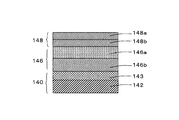
- 10 is a schematic cross-sectional view showing a layer configuration of an electrode foil produced in Example 8.
- FIG. 10 is a schematic cross-sectional view showing a layer configuration of an organic EL element produced in Example 9.
- FIG. 10 is a schematic cross-sectional view showing a layer configuration of an organic EL element produced in Example 9.
- FIG. 1 shows a schematic cross-sectional view of an example of an electrode foil according to the present invention.
- An electrode foil 10 shown in FIG. 1 includes a metal foil 12, a reflective layer 13 provided directly on the metal foil, and a buffer layer 14 provided directly on the reflective layer as required. That is, the electrode foil 10 has a three-layer configuration including the metal foil 12, the reflective layer 13, and the buffer layer 14, but the electrode foil of the present invention is not limited to this, and the two-layer configuration of the metal foil 12 and the reflective layer 13 It may be.
- a reflective layer is generally formed on a metal electrode layer, but it is believed that this metal electrode layer must be formed on a supporting substrate such as an insulating substrate. Has been.
- the metal foil 12 is used not only as a support base material but also as an electrode, and the reflective layer 13 is directly provided on the metal foil 12, thereby having the three functions of the support base material, the electrode, and the reflective layer. It is possible to provide an electrode foil that has never existed before. Therefore, according to the electrode foil of this invention, the support base material and reflection layer which were required by the conventional top emission type flexible light-emitting device can be made unnecessary. For this reason, the electrode foil of the present invention does not have an insulating layer at least on the reflective layer side, and preferably does not have an insulating layer in any part.
- the metal foil 12 is not particularly limited as long as it is a foil-like metal material having strength as a supporting substrate and electrical characteristics required as an electrode.
- a preferred metal foil is a nonmagnetic metal foil from the viewpoint of preventing adhesion of particulate matter generated during processing due to magnetism.
- the nonmagnetic metal include copper, aluminum, nonmagnetic stainless steel, titanium, tantalum, molybdenum, and the like, and copper, aluminum, and nonmagnetic stainless steel are more preferable.
- the most preferred metal foil is a copper foil. Copper foil is excellent in strength, flexibility, electrical characteristics and the like while being relatively inexpensive.
- At least one outermost surface of the electrode foil 10 is preferably an ultra flat surface having an arithmetic average roughness Ra of 10.0 nm or less, more preferably 7.0 nm or less, still more preferably 5.0 nm, and even more preferably. Is 3.0 nm or less, particularly preferably 2.8 nm or less, particularly preferably 2.5 nm or less, and most preferably 2.0 nm or less.
- the lower limit of the arithmetic average roughness Ra is not particularly limited and may be zero. However, in consideration of the efficiency of the flattening process, 0.5 nm is cited as a guideline for the lower limit value.
- This arithmetic average roughness Ra can be measured using a commercially available roughness measuring device in accordance with JIS B 0601-2001.
- At least one outermost surface of the electrode foil 10 means the surface 13a of the reflective layer 13 in the case of a two-layer structure, and the surface 14a of the buffer layer 14 in the case of a three-layer structure.
- the arithmetic average roughness Ra on the surface 13a of the reflective layer 13 is realized by setting the arithmetic average roughness Ra of the surface 12a of the metal foil 12 on which the reflective layer 13 is formed in the same manner as described above. In the range of 10.0 nm or less, preferably 6.0 nm or less, more preferably 3.0 nm or less, still more preferably 2.0 nm or less, and even more preferably 1.5 nm or less.
- arithmetic average roughness Ra on the surface 14a of the buffer layer 14 in the case of a three-layer structure is 10.0 nm or less, preferably 6.5 nm or less, more preferably 3.0 nm or less, and more preferably as described above.
- the surface 14a of the buffer layer 14 thus formed has a thickness of 10.0 nm or less, preferably 7.0 nm or less, more preferably 5.0 nm, even more preferably 3.0 nm or less, particularly preferably 2.8 nm or less, particularly more
- the arithmetic average roughness Ra is preferably 2.5 nm or less. As described above, it is preferable that an arithmetic average roughness Ra that is equal to or slightly smaller than the arithmetic average roughness Ra to be applied on the outermost surface is provided on the surface of the lower layer or foil.
- the arithmetic average roughness Ra of the surface of the metal foil that does not constitute the outermost surface due to the laminated state is evaluated by creating a cross section from the surface of the metal foil by FIB (Focused Ion Beam) processing, and using the transmission electron microscope (TEM), and the arithmetic average roughness Ra of the reflective layer surface that does not constitute the outermost surface due to the laminated state can be evaluated in the same manner.
- FIB Flucused Ion Beam
- metal foils especially copper foils having such an ultra-flat surface have not been industrially produced until now, and even attempts to apply them as electrodes of flexible electronic devices are not possible. It has never been done before.
- copper foil with a flattened surface is commercially available, the level of flattening of such a copper foil is insufficient as an electrode for an organic EL element, and short-circuits due to surface irregularities in the case of an organic EL element. There is a risk that light emission may not be obtained.
- Such an ultra-flat surface can be realized by polishing a metal foil by CMP (Chemical Mechanical Polishing).
- CMP Chemical Mechanical Polishing
- the CMP treatment can be performed according to known conditions using a known polishing liquid and a known polishing pad.
- a preferred polishing liquid contains about 0.5 to 2% by weight of one or more abrasive grains selected from ceria, silica, alumina, zirconia and the like, and an oxidizing agent such as benzotriazole (BTA).
- a preferable polishing pad includes a urethane pad.
- the polishing conditions are not particularly limited as long as the pad rotation speed, work load, polishing liquid application flow rate, etc. are adjusted appropriately, but the rotation speed is in the range of 20 to 1000 rpm, and the work load is in the range of 100 to 500 gf / cm 2 . In addition, it is preferable to adjust the polishing liquid application flow rate within the range of 20 to 200 cc / min.
- the ultra-flat surface 12a can also be realized by polishing the metal foil 12 using an electrolytic polishing method, a buff polishing method, a chemical polishing method, or a combination thereof.
- the chemical polishing method is not particularly limited as long as the chemical solution, the chemical solution temperature, the chemical solution immersion time, etc. are appropriately adjusted.
- the chemical polishing of copper foil uses a mixture of 2-aminoethanol and ammonium chloride. Can be performed.
- the temperature of the chemical solution is preferably room temperature, and it is preferable to use an immersion method (Dip method). Further, since the chemical solution immersion time tends to deteriorate the flatness as it becomes longer, it is preferably 10 to 120 seconds, and more preferably 30 to 90 seconds.
- the metal foil after chemical polishing is preferably washed with running water. According to such a planarization process, it is possible to planarize a surface having a Ra arithmetic average roughness Ra of about 12 nm to Ra 10.0 nm or less, for example, about 3.0 nm.
- the ultra-flat surface 12a may be realized by a method of polishing the surface of the metal foil 12 by blasting, a method of rapidly cooling the surface of the metal foil 12 by melting it by a technique such as laser, resistance heating, or lamp heating. it can.
- a metal foil that can be plated such as copper, nickel, or chrome
- an ultra-flat surface can be realized using a transfer method.
- the transfer method may be performed based on a known method and known conditions. For example, the surface of the electrode plate made of SUS, titanium, or the like is planarized using an electrolytic polishing method and a buff polishing method so that the arithmetic average roughness Ra is 10.0 nm or less, for example, 3.0 nm or less.
- the material of the metal foil 12 is plated on the surface of the flattened electrode plate, and when the desired thickness is reached, the material of the metal foil 12 is peeled off from the electrode plate.
- an ultra-flat surface can be realized.
- the thickness of the metal foil 12 is not particularly limited as long as it is a thickness that can be handled alone as a foil without impairing flexibility, but it is 1 to 250 ⁇ m, preferably 25 to 250 ⁇ m, more preferably 35 to 150 ⁇ m. is there. With such a thickness, it is possible to easily cut using a commercially available cutting machine.
- the metal foil 12 has no problems such as cracking and chipping, and has advantages such as less generation of particles during cutting.
- the metal foil 12 can have various shapes other than a quadrangle, for example, a circle, a triangle, a polygon, and can be cut and welded. It is also possible to produce a light emitter. In this case, it is preferable not to form a light emitting layer at the cut portion or welded portion of the metal foil 12.
- the ultra flat surface 12a is preferably washed with an alkaline solution.
- an alkaline solution a known alkaline solution such as a solution containing ammonia, a sodium hydroxide solution, or a potassium hydroxide solution can be used.
- a preferred alkaline solution is a solution containing ammonia, more preferably an organic alkaline solution containing ammonia, and even more preferably a tetramethylammonium hydroxide (TMAH) solution.
- TMAH tetramethylammonium hydroxide
- a preferable concentration of the TMAH solution is 0.1 to 3.0 wt%.
- cleaning is performed at 23 ° C. for 1 minute using a 0.4% TMAH solution.
- the same cleaning effect can be obtained by performing UV (Ultra Violet) treatment in combination with the cleaning with the alkaline solution or in place of the cleaning with the alkaline solution.
- UV Ultra Violet
- an acidic cleaning solution such as dilute sulfuric acid.
- the acid cleaning it is possible to perform cleaning for 30 seconds using dilute sulfuric acid.
- the dry ice blasting method is a method of removing particles by spraying carbon dioxide, which has been solidified at a low temperature, onto the ultra-flat surface 12a by spraying carbon dioxide gas compressed to a high pressure from a thin nozzle. Unlike the wet process, this dry ice blasting method has the advantages that the drying process can be omitted and organic substances can be removed.
- the dry ice blasting method can be performed using a commercially available apparatus such as a dry ice snow system (manufactured by Air Water).
- the reflective layer 13 is directly provided on the ultra flat surface of the metal foil 12.
- the reflective layer 13 is preferably composed of at least one selected from the group consisting of aluminum, aluminum-based alloys, silver, and silver-based alloys. These materials are suitable for the reflective layer because of their high light reflectivity, and also have excellent flatness when thinned.
- aluminum or an aluminum-based alloy is preferable because it is an inexpensive material.
- an aluminum alloy and a silver alloy those having a general alloy composition used as an anode or a cathode in a display device such as an organic EL element can be widely used.
- Examples of preferable aluminum-based alloy compositions include Al—Ni, Al—Cu, Al—Ag, Al—Ce, Al—Zn, Al—B, Al—Ta, Al—Nd, Al—Si, Al—La, Examples include Al—Co, Al—Ge, Al—Fe, Al—Li, Al—Mg, and Al—Mn alloys. Any element constituting these alloys can be arbitrarily combined according to the required characteristics.
- Examples of preferable silver alloy compositions include Ag—Pd, Ag—Cu, Ag—Al, Ag—Zn, Ag—Mg, Ag—Mn, Ag—Cr, Ag—Ti, Ag—Ta, and Ag—Co.
- the thickness of the reflective layer 13 is not particularly limited, but preferably has a thickness of 30 to 500 nm, more preferably 50 to 300 nm, and still more preferably 100 to 250 nm.
- the surface 13a of the reflective layer 13 is preferably 10.0 nm or less, more preferably 6.5 nm or less, still more preferably 3.0 nm or less, even more preferably 2.5 nm or less, particularly preferably 2.0 nm or less.
- Has Ra As described above, since the reflective layer is formed on the surface of the ultra-flat metal foil in the electrode foil of the present invention, high flatness can be realized by reducing the arithmetic average roughness Ra also on the surface of the reflective layer. Thereby, the risk of a short circuit between organic EL layers due to the occurrence of excessive unevenness can be reduced.
- these layers and organic EL layers containing them are conventionally provided. It can be made thinner. As a result, the production cost can be reduced by reducing the amount of extremely expensive organic raw materials used, and the light emission efficiency can be improved by reducing the thickness of the organic EL layer.
- the reflective layer 13 is composed of an aluminum film or an aluminum alloy film
- the reflective layer may be composed of a laminated structure composed of at least two layers as shown in FIG. That is, the electrode foil 50 shown in FIG. 9 has the metal foil 52, the reflective layer 53, and the desired buffer layer 54 as in the electrode foil 10 shown in FIG. 1, but the reflective layer 53 is partitioned by the interface 53c. It has a laminated structure of two layers 53a and 53b, and the lower layer 53a and the upper layer 53b have different crystal orientations with the interface 53c as a boundary. This effectively suppresses the thermal migration that can occur from the interface between the copper foil and the aluminum-containing reflective layer, even when the electrode foil is exposed to a considerably high temperature, resulting in surface flatness caused by thermal migration.
- the heat resistance of the electrode foil can be improved. Therefore, it can be said that this aspect is particularly effective in the heat treatment after coating the hole injection layer performed at a temperature of 200 ° C. or higher, preferably 230 ° C. or higher, more preferably 250 ° C. or higher.
- Such an improvement in heat resistance is considered to be realized by preventing thermal migration that proceeds with priority given to the crystal grain boundaries by the interface 53c where the crystal grain boundaries become discontinuous.
- the number of interfaces 53c in the reflective layer 53 may be two or more. In this case, the reflective layer has a laminated structure of three or more layers.
- the reflective layer 53 having a laminated structure can be produced by performing a film formation process such as sputtering a plurality of times at predetermined intervals.
- a film formation process such as sputtering a plurality of times at predetermined intervals.
- Preferred examples of such a method include the following. (1) The lower layer 53a is preferably formed by sputtering until the thickness reaches 10 nm or more, and the sputtering is temporarily stopped. In this state, the lower layer 53a is left in the chamber of the sputtering apparatus. This standing time is preferably 30 seconds or longer. Next, sputtering is resumed to form the upper layer 53b. (2) The lower layer 53a is preferably formed by sputtering until the thickness reaches 10 nm or more, and the sputtering is temporarily stopped.
- the lower layer 53a is brought into contact with the atmosphere.
- the metal foil on which the lower layer 53a is formed may be taken out from the chamber of the sputtering apparatus and exposed to the atmosphere, or the chamber may be released to the atmosphere without taking out the metal foil.
- sputtering is resumed to form the upper layer 53b.
- the time required to expose the lower layer 53a to the atmosphere is about several seconds, and the desired effect can be obtained at the humidity and temperature as in a normal clean room environment.
- the lower layer 53a is preferably formed by sputtering until the thickness becomes 10 nm or more, and the sputtering is temporarily stopped.
- the upper layer 53b is formed by evacuation again.
- the pressure in the chamber into which oxygen is introduced is preferably 0.01 Pa or more, more preferably 0.1 Pa or more, and further preferably 1 Pa or more.
- one interface 53c is sufficient. Even one interface exhibits sufficient heat resistance at a high temperature of about 250 ° C. However, the heat resistance may be further improved by increasing the number of film formation processes and providing two or more interfaces.
- the buffer layer 14 is directly provided on the reflective layer 13.
- the buffer layer 14 is not particularly limited as long as it is in contact with the organic EL layer in the organic EL element to improve the hole injection efficiency or the electron injection efficiency and provide a desired work function.
- the buffer layer in the present invention is preferably transparent or translucent from the viewpoint of allowing the metal foil to function as a reflective layer.
- the buffer layer 14 is preferably at least one selected from a conductive amorphous carbon film, a conductive oxide film, a magnesium-based alloy film, and a fluoride film, and is used and required as an anode or a cathode. What is necessary is just to select suitably according to a characteristic.
- the conductive amorphous carbon film various amorphous carbon films imparted with conductivity by controlling the hydrogen concentration or impurity concentration can be used.
- the formation of the conductive amorphous carbon film is preferably performed by a sputtering method.
- a carbon target used for sputtering it is desirable to use a purified product. It is also possible to use porous carbon impregnated with B, Si, Al, Cu.
- a conductive amorphous carbon film is used as a buffer layer, an aluminum film, an aluminum-based alloy film, a silver film, and a silver-based alloy film are all suitable as a reflective layer, but considering flatness and material cost Aluminum alloys are preferred.
- a preferable conductive amorphous carbon film is composed of conductive amorphous carbon having a hydrogen concentration of 15 at% or less.
- a more preferable hydrogen concentration is 12 at% or less, and further preferably 5 at% or less.
- the lower limit of the hydrogen concentration is not particularly limited and may be zero. However, considering the inevitable mixing of hydrogen due to the film formation environment during sputtering, 3 at% is an example of the lower limit.
- the hydrogen concentration in the buffer layer can be measured by various known methods, but is preferably performed by HFS (hydrogen forward scattering). In this specification, the hydrogen concentration in the conductive amorphous carbon film is defined as the hydrogen concentration when carbon and hydrogen are quantified with HFS or the like and the total number of these atoms is 100 at%.
- the conductive amorphous carbon is not substantially doped with impurities other than carbon and hydrogen.
- substantially undoped means that impurities are not intentionally doped in order to provide some function, and inevitably mixed due to the film forming environment during sputtering. Impurities are allowed.
- the conductive amorphous carbon in the present invention preferably has an oxygen concentration of 0 to 300 wtppm, a halogen element concentration of 0 to 1000 wtppm, and a nitrogen concentration of 0 to 500 wtppm.
- the thickness of the buffer layer 14 is not particularly limited, but is preferably 3 to 30 nm, more preferably 3 to 15 nm, and still more preferably 5 to 10 nm.
- Preferred InO x as the conductive oxide film SnO x, ZnO x, MoO x, GaO x, VO x, WO x, RuO x, AlO x, 1 kind selected from the group consisting of TiO x, and GeO x or
- a film composed of two or more kinds is exemplified, and typical examples include ITO (indium tin oxide) and IZO (indium zinc oxide).
- the conductive oxide film may be formed by a known method such as a sputtering method or a vacuum deposition method, and is preferably performed by a DC magnetron sputtering method.
- the target material used for the sputtering method can be manufactured by a hot press method or a cold press method, desired characteristics can be obtained by appropriately combining the above oxides.
- a conductive oxide film is used as the buffer layer, an Al—Ni alloy, Ag, or an Ag alloy is particularly suitable as the reflective layer.
- a preferable magnesium-based alloy film includes a film made of an alloy in which one or more selected from Ag, Al, Zn, Li, Y, and Ca are added to Mg.
- the magnesium-based alloy film may be formed by a known method such as a sputtering method or a vacuum deposition method, and is preferably performed by a vacuum deposition method.
- Preferable fluoride films include films composed of one or more selected from LiF, MgF 2 , CaF 2 , AlF 3 , Na 3 AlF 6 and NaF 6 .
- the fluoride film may be formed by a known method such as a sputtering method or a vacuum deposition method, and is preferably performed by a vacuum deposition method.
- the surface 14a of the buffer layer 14 is preferably 10.0 nm or less, more preferably 7.0 nm or less, still more preferably 5.0 nm, even more preferably 3.0 nm or less, particularly preferably 2.8 nm or less, and particularly preferably Arithmetic average roughness Ra of 2.5 nm or less.
- the buffer layer is formed on the surface of the ultra-flat reflective film caused by the ultra-flat metal foil. Therefore, the arithmetic average roughness Ra is reduced and increased also on the surface of the buffer layer. Flatness can be realized. Thereby, the risk of a short circuit between organic EL layers due to the occurrence of excessive unevenness can be reduced.
- these layers and the organic EL layer containing them are conventionally provided. It can be made thinner. As a result, the production cost can be reduced by reducing the amount of extremely expensive organic raw materials used, and the light emission efficiency can be improved by reducing the thickness of the organic EL layer.
- An oxide film (not shown) may exist between the reflective layer 13 and the buffer layer 14. This oxide film is typically formed by unavoidably oxidizing the anode layer with oxygen in the atmosphere. Such an oxide film is preferably as thin as possible, and a preferable thickness is 3.0 nm or less, and more preferably 1.5 nm or less. Such an oxide film may be removed by etching or the like.
- the electrode foil according to the present invention preferably has a thickness of 1 to 300 ⁇ m, more preferably 25 to 250 ⁇ m, still more preferably 35 to 150 ⁇ m, and most preferably 40 to 100 ⁇ m.
- the surface 12b of the metal foil 12 opposite to the reflective layer 13 has a 10-point average roughness of 1.0 ⁇ m or more, more preferably 2.0 ⁇ m or more, and even more preferably 5.0 ⁇ m or more.
- the ten-point average roughness Rz can be measured using a commercially available roughness measuring device in accordance with JIS B 0601-1994.
- This roughening process can be preferably performed by a known method such as dry ice blasting, sand blasting, wet etching, or dry etching.
- the heat dissipation characteristics can be improved by the unevenness formed on the surface of the roughened surface.
- the electrode foil according to the present invention is based on a metal foil, it can be efficiently produced by, for example, a roll-to-roll process without particularly requiring a supporting substrate.
- the electrode foil according to the present invention can be preferably used as an anode or a cathode for various flexible electronic devices (particularly flexible light-emitting or power-generating devices), thereby functioning as a reflective electrode.
- flexible electronic devices include organic EL elements, organic EL lighting, organic EL displays, electronic paper, thin film solar cells, liquid crystal displays, inorganic EL elements, inorganic EL displays, LED lighting, and LED displays.
- the organic EL element is preferably an organic EL element, an organic EL illumination, an organic EL display, an organic solar cell, or a dye-sensitized solar cell, and more preferably an organic EL illumination in that ultra-thin and high-luminance emission can be obtained.
- the electrode foil according to the present invention can be preferably used as an anode or a cathode of the organic solar cell.
- the organic device can be configured as either an organic EL element or an organic solar cell by appropriately selecting the type of the organic semiconductor layer to be laminated on the electrode foil according to the present invention in accordance with a known technique.
- a light emitting element and a power generating element can be formed on the same electrode at the same time, whereby a composite device having both the function of an organic EL element and the function of an organic solar cell can be manufactured.
- the electrode foil according to the present invention can be used not only for electrodes of organic EL elements but also for LED mounting substrates.
- the electrode foil according to the present invention can be preferably used as an anode or a cathode for LED illumination in that LED elements can be densely mounted.
- Organic EL Element and Organic EL Lighting Using the electrode foil according to the present invention as a reflective electrode, a top emission type organic EL element and organic EL lighting can be constructed.
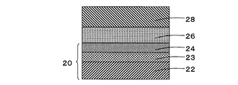
- FIG. 2 shows an example of a layer structure of a top emission type organic EL element using the electrode foil of the present invention as an anode.
- the organic EL element shown in FIG. 2 includes an anode electrode foil 20 including a metal foil 22, a reflective layer 23, and a buffer layer 24, an organic EL layer 26 provided directly on the buffer layer 24, and an organic EL layer 26. And a cathode 28 as a counter electrode provided directly.
- the buffer layer 24 is preferably composed of a conductive amorphous carbon film or a conductive oxide film so as to be suitable as an anode.
- organic EL layer 26 various known EL layer configurations used for organic EL elements can be used.
- the electron injection layer may be sequentially provided from the anode electrode foil 20 toward the cathode 26.
- layers having various known configurations and compositions can be used as appropriate, and are not particularly limited.
- an organic solar cell can be configured by replacing the organic EL layer 26 with a known organic solar cell active layer.
- a hole transport layer PEDOT: PSS (30 nm)
- a p-type organic semiconductor layer for example, BP (benzoporphyrin) are formed on a buffer layer (for example, a carbon buffer layer).
- An i-type mixing layer of an n-type organic semiconductor and a p-type organic semiconductor for example, BP: PCBNB (fullerene derivative)
- an n-type organic semiconductor layer for example, PCBM (fullerene derivative)
- a buffer layer having a low work function for example, a solar cell can be formed by sequentially laminating Mg—Ag) and a transparent electrode layer (for example, IZO).
- a known material can be appropriately used as a material constituting each of these layers, and is not particularly limited.
- the electrode used for the organic solar cell may have the same material and structure as the electrode used for the organic EL element.
- the electrode foil of the present invention is expected to improve the power generation efficiency due to light confinement due to the cavity effect by providing the reflective layer.
- FIG. 3 shows an example of a layer configuration of a top emission type organic EL lighting in which the organic EL element shown in FIG. 2 is incorporated.
- the organic EL element can be electrically connected to the power source 30 through the metal foil 22 of the anode electrode foil 20.
- a region on the buffer layer 24 that is not in contact with the organic EL layer 26 is covered with an interlayer insulating film 29.
- the interlayer insulating film 29 a Si-based insulating film formed by CVD is preferable because it has a high barrier property against moisture and oxygen that cause deterioration of the organic layer, and more preferably a SiN-based insulating film.
- a more preferred interlayer insulating film is a SiNO insulating film in that the internal stress of the film is small and the flexibility is excellent.
- a sealing material 32 is provided above the cathode 28 so as to face the organic EL element, and a sealing resin 34 is filled between the sealing material 32 and the organic EL element 20 to form a sealing film 34.
- the sealing material 32 glass or a film can be used. In the case of glass, it can be directly bonded onto the sealing film 34 using a hydrophobic adhesive tape. In the case of a film, both surfaces and end surfaces can be covered with a Si-based insulating film. When a film having a high barrier property is developed in the future, it is possible to perform sealing without performing a coating treatment, and it is expected that the film has excellent mass productivity.
- a film is desirable from the viewpoint of imparting flexibility, but a desired performance is obtained by using a sealing material in which a film is bonded to a very thin glass having a thickness of 20 to 100 ⁇ m. It is also possible.
- cathode 28 various known cathodes used for top emission type organic EL elements can be used, and since it is necessary to transmit light, it is not particularly limited as long as it is transparent or translucent. A low one is preferred.
- Preferred cathodes include conductive oxide films, magnesium-based alloy films, and fluoride films, and it is more preferable to combine these in two or more layers. These films can be the same as those described for the buffer layer of the electrode foil.
- a particularly preferable cathode has a two-layer structure in which a transparent oxide layer as a cathode layer made of a conductive oxide film is laminated with a semi-transmissive metal layer as a buffer layer made of a magnesium alloy film and / or a fluoride film.
- a semi-transmissive metal layer as a buffer layer made of a magnesium alloy film and / or a fluoride film.
- the most preferred example is a cathode structure in which a transparent oxide layer (cathode layer) made of IZO (indium zinc oxide) and a semi-transmissive metal layer (buffer layer) made of Mg—Ag are laminated. Further, the cathode structure may include two or more transparent oxide layers and / or two or more semi-transmissive metal layers.
- the light generated in the organic EL layer 26 passes through the cathode 28, the sealing film 34, and the sealing material 32 and is emitted to the outside.
- assistant base material suitably in the back surface of the electrode foil 20 according to a usage form. Since this portion does not affect the light emission characteristics, the degree of freedom in material selection is high. For example, if resin films such as polyethylene terephthalate (PET), polyimide (PI), polycarbonate (PC), polyethersulfone (PES), and polyethernitrile (PEN) are used, the flexibility will not be impaired, so it is optimal. I can say that.
- PET polyethylene terephthalate
- PI polyimide
- PC polycarbonate
- PES polyethersulfone
- PEN polyethernitrile
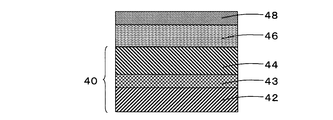
- FIG. 4 shows an example of a layer structure of a top emission type organic EL element using the electrode foil of the present invention as a cathode.
- the organic EL element shown in FIG. 4 includes a cathode electrode foil 40 including a metal foil 42, a reflective layer 43, and a buffer layer 44, an organic EL layer 46 provided directly on the buffer layer 44, and an organic EL layer 46. And an anode 48 as a counter electrode provided directly.
- the organic EL layer 46 can be configured in the same manner as the organic EL layer 26 shown in FIG. 2, and the buffer layer 44 can be configured in the same manner as the cathode 28 shown in FIG. It is preferably composed of a system alloy film, a fluoride film, or a combination of two or more layers thereof.
- a more preferable buffer layer 44 is a semi-transmissive metal layer made of a magnesium-based alloy film and / or a fluoride film.
- the organic EL element using the cathode electrode foil 40 shown in FIG. 4 is the same as the organic EL element using the anode electrode foil 20 shown in FIG. 26 corresponds to a configuration in which the stacking order from the anode side to the cathode side in the interior 26 is reversed.
- a magnesium alloy film or a fluoride film is formed as the buffer layer 44 of the cathode electrode foil 40 by sputtering or vapor deposition, while a conductive amorphous carbon, MoO 3 or V 2 O 5 film is vapor deposited as the anode 48. It is preferable to form by.
- a conductive amorphous carbon film is formed on the organic EL layer, it is preferable to use a vacuum deposition method in order to avoid plasma damage during sputtering.
- Example 1 Preparation of Cu / Al alloy / ITO electrode foil As a metal foil, a commercially available double-sided flat electrolytic copper foil having a thickness of 64 ⁇ m (DFF (Dual Flat Foil) manufactured by Mitsui Metal Mining Co., Ltd.) was prepared.
- DFF Double Flat Foil
- This copper foil was subjected to a CMP (Chemical Mechanical Polishing) process using a polishing machine manufactured by MTT.
- This CMP treatment was performed using a polishing pad with XY grooves and a colloidal silica-based polishing liquid under the conditions of pad rotation speed: 30 rpm, load: 200 gf / cm 2 , and liquid supply amount: 100 cc / min.
- the roughness of the copper foil surface thus treated with CMP was measured in accordance with JIS B 0601-2001 using a scanning probe microscope (Veeco, Nano Scope V). The arithmetic average roughness Ra was 0.7 nm. Met. This measurement was performed by Tapping Mode AFM for a range of 10 ⁇ m square.
- the thickness of the copper foil after the CMP treatment was 48 ⁇ m.
- a 150 nm-thick Al alloy reflective layer was formed on the surface of the CMP-treated copper foil by sputtering.
- This sputtering is performed using a magnetron sputtering apparatus (MSL-) in which an aluminum alloy target (diameter 203.2 mm ⁇ 8 mm thickness) having a composition of Al-0.2B-3.2Ni (at.%) Is connected to a cryo pump. 464, manufactured by Tokki Co., Ltd.), input power (DC): 1000 W (3.1 W / cm 2 ), ultimate vacuum: ⁇ 5 ⁇ 10 ⁇ 5 Pa, sputtering pressure: 0.5 Pa, Ar flow rate: The measurement was performed under the conditions of 100 sccm and substrate temperature: room temperature.
- MSL- magnetron sputtering apparatus
- An ITO buffer layer having a thickness of 10 nm was formed on the surface of the aluminum alloy reflective layer thus obtained by sputtering.
- an ITO (In 2 O 3 —SnO 2 ) target (diameter 203.2 mm ⁇ 6 mm thickness) containing 10% by weight of Sn is connected to a magnetron sputtering apparatus (MSL-464, Tokki) to which a Cryo pump is connected.
- Example 2 Preparation of Cu / Al alloy / C electrode foil An electrode foil was prepared in the same manner as in Example 1 except that a carbon buffer layer having a film thickness of 1.7 nm or 3.5 nm was formed by sputtering instead of the ITO buffer layer. Produced. As a carbon target for this sputtering, an untreated carbon target with a purity of 3N (99.9%) made from a carbon material (IGS743 material, manufactured by Tokai Carbon Co., Ltd.) and a purification treatment with halogen gas on this carbon material. Two types of carbon targets having a purity of 5N (99.999%) were prepared. A carbon buffer layer was formed by sputtering using each of these targets.
- a carbon buffer layer having a film thickness of 1.7 nm or 3.5 nm was formed by sputtering instead of the ITO buffer layer.
- each carbon target (diameter 203.2 mm ⁇ 8 mm thickness) was mounted on a magnetron sputtering apparatus (multi-chamber single-wafer type film forming apparatus MSL-464, manufactured by Tokki Co., Ltd.) connected to a cryo pump.
- ultimate vacuum ⁇ 5 ⁇ 10 ⁇ 5 Pa
- sputtering pressure 0.5 Pa
- Ar flow rate 100 sccm
- substrate temperature room temperature.
- the film thickness was controlled by controlling the discharge time.
- the roughness of the buffer layer surface thus obtained was measured in the same manner as in Example 1, the arithmetic average roughness Ra was 2.45 nm.
- the total thickness of the obtained electrode foil was 48 ⁇ m.
- Example 3 Preparation of Cu / Ag alloy / ITO electrode foil A buffer layer and a reflective layer were provided in the same manner as in Example 1 except that a 150 nm-thick Ag alloy reflective layer was formed by sputtering instead of the Al alloy reflective layer. An electrode foil is prepared.
- a magnetron sputtering apparatus MSL- in which a silver alloy target (diameter 101.6 mm ⁇ 5 mm thickness) having a composition of Ag-1.0Cu-1.0Pd (at.%) Is connected to a Cryo pump.
- Example 4 Production of Organic EL Element An organic EL element having a structure as shown in FIGS. 2 and 3 was produced using the electrode foil (Cu / Al alloy / ITO) produced in Example 1 as an anode.
- a glass substrate (3 cm square ⁇ 0.5 mm thickness) was placed on the electrode foil 20 (5 cm square) for masking, and an interlayer insulating film 29 made of silicon nitride was formed by a plasma CVD (Chemical Vapor Deposition) method.
- This plasma CVD uses a plasma CVD apparatus (PD2202L, manufactured by Samco) connected with a mechanical booster pump (MBP) and a rotary pump (RP).
- the surface of the electrode foil on which the interlayer insulating film was formed was washed as follows. First, in a tank filled with ultrapure water (> 18.0 M ⁇ ), ultrasonic cleaning for 3 minutes was performed twice by replacing ultrapure water. Subsequently, after moisture was removed using nitrogen gas, after-curing was performed at 100 ° C. for 3 hours. The surface thus treated was cleaned by UV irradiation.
- ultrapure water > 18.0 M ⁇
- the organic EL layer 26, the cathode 28, the sealing layer 34, and the sealing material 32 were laminated. Specifically, a 50-nm-thick hole injection layer made of copper phthalocyanine, 4,4′-bis (N, N ′-(3-tolyl) amino) -3,3 ′ is formed on the buffer layer surface of the electrode foil.
- a hole transport layer made of dimethylbiphenyl (HMTPD) with a thickness of 40 nm, a light emitting layer with a thickness of 30 nm formed by doping tris (2-phenylpyridine) iridium complex (Ir (ppy) 3 ) in a host material, Alq3 A 30 nm thick electron transport layer, a 10 nm thick Mg—Ag semi-transmissive film layer (Mg: Ag 9: 1), a 100 nm thick IZO (In—Zn—O) transparent oxide layer, a thickness A 300 nm silicon nitride passivation film (sealing layer), a 2000 nm thick adhesive layer, and a 200 ⁇ m thick sealing glass (sealing material) were laminated in this order.
- HMTPD dimethylbiphenyl
- the sealing glass layer is laminated with a double-sided tape, and this double-sided tape corresponds to the adhesive layer.
- an organic EL element sample having a size of 50 mm square x thickness of 300 ⁇ m and a light emitting area of 30 mm square as shown in FIG. 3 was obtained.
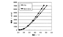
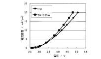
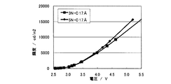
- a voltage of 5.0 V was applied, strong light emission as shown in FIG. 5 could be confirmed.
- the change in luminance (cd / m 2 ) and current density (mA / cm 2 ) was measured by changing the applied voltage, the results shown in FIG. 6 and FIG. 7 were obtained (“ITO” in the figure). ”).
- ITO in the figure.
- Example 5 Preparation of organic EL element 3
- the electrode foil (Cu / Al alloy / C) having the following three types of carbon buffer layers prepared in Example 2 was used.
- Various types of organic EL element samples were prepared.
- Sample “3N-C 17 ⁇ ” an organic EL element using a carbon buffer layer having a thickness of 1.7 nm formed using a carbon target having a purity of 3N
- Sample “5N-C 17 ⁇ ” carbon having a purity of 5N
- each of the samples was connected to a power supply 30 as shown in FIG.
- changes in luminance (cd / m 2 ) and / or current density (mA / cm 2 ) were measured by changing the applied voltage, the results shown in FIGS. 6 to 8 were obtained.
- the electrode foil of the present invention when used, light emission with extremely high luminance can be obtained at a low voltage.
- Example 6 Preparation of Cu / Al alloy / Al alloy / ITO electrode foil Example 1 except that an Al alloy reflective layer having a two-layer structure composed of an upper layer and a lower layer was formed by two-stage sputtering through standing in a vacuum. An electrode foil was produced basically in the same manner. In this two-stage sputtering, a lower layer having a thickness of 50 nm is formed on a metal foil under the same conditions as those of the Al alloy reflective layer of Example 1, and the sputtering is temporarily stopped, and the metal foil is vacuum-evacuated as it is in a chamber.
- the film was allowed to stand for about 30 seconds, and sputtering was resumed under the same conditions as described above to form an upper layer having a thickness of 100 nm on the lower layer.
- the overall thickness of the electrode foil thus obtained was 48 ⁇ m.
- the cross section of the electrode foil thus obtained was observed with a transmission electron microscope (TEM), the micrograph shown in FIG. 10 was obtained.
- the reflective layer has a laminated structure composed of two layers separated by an interface that appears to be amorphous with a thickness of about 1 nm, and the two layers have different crystal orientations ( It was observed that the lower layer has a generally horizontal direction and the upper layer has a generally vertical direction.
- Example 7 Preparation of Cu / Al alloy / Al alloy / ITO electrode foil Example 1 except that an Al alloy reflective layer having a two-layer structure consisting of an upper layer and a lower layer was formed by two-step sputtering through standing in the atmosphere. Similarly, an electrode foil was produced. In this two-stage sputtering, a lower layer having a thickness of 50 nm is formed on the metal foil under the same conditions as those of the Al alloy reflective layer of Example 1, and the sputtering is temporarily stopped, and the metal foil is taken out of the chamber into the atmosphere.
- the metal foil was returned to the chamber again for about 30 seconds, and sputtering was resumed under the same conditions as described above to form an upper layer having a thickness of 100 nm on the lower layer.
- the overall thickness of the electrode foil thus obtained was 48 ⁇ m.
- the cross section of the electrode foil thus obtained was observed with a TEM, the micrograph shown in FIG. 12 was obtained.
- the reflective layer had a laminated structure composed of two layers separated by an interface, and the two layers had different crystal orientations with the interface as a boundary.
- EDX analysis was performed on the interface of the obtained reflective layer, a spectrum having peaks derived from Al and O as shown in FIG. 13 was obtained.
- the oxygen component was detected from the interface, it is understood that the natural oxide film constitutes the interface.
- Example 8 Preparation of Cu / Al Alloy Electrode Foil
- an Al alloy reflective layer 143 with a film thickness of 150 nm was formed by sputtering on a copper foil 142 manufactured under the same conditions as in Example 1. .
- This sputtering is performed using a magnetron sputtering apparatus (MSL-464, manufactured by Tokki Co., Ltd.) in which an aluminum alloy target (diameter 203.2 nm ⁇ 8 mm thickness) having a composition of Al-4Mg (at.%) Is connected to a Cryo pump.
- MSL-464 magnetron sputtering apparatus
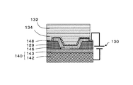
- Example 9 Production of Organic EL Device Using the electrode foil 140 (Cu / Al alloy) produced in Example 8 as a cathode, an organic EL device having a structure as shown in FIGS. 14 and 15 was produced. First, a glass substrate (3 cm square ⁇ 0.5 mm thickness) was placed on the electrode foil 140 (5 cm square) for masking, and an interlayer insulating film 29 made of silicon nitride was formed by a plasma CVD (Chemical Vapor Deposition) method. This plasma CVD uses a plasma CVD apparatus (PD2202L, manufactured by Samco) connected with a mechanical booster pump (MBP) and a rotary pump (RP).
- P2202L plasma CVD apparatus
- MBP mechanical booster pump
- RP rotary pump
- the organic EL layer 146, the anode 148, the sealing layer 134, and the sealing material 132 were laminated on the electrode foil thus cleaned.
- an ⁇ -NPD layer 146b with a thickness of 50 nm, an Alq3 layer 146a with a thickness of 50 nm, a MoO 3 layer 148b with a thickness of 20 nm, an IZO (In—Zn) with a thickness of 100 nm are formed on the surface of the reflective layer 143 of the electrode foil.
- a transparent oxide layer 148a, a 300 nm thick silicon nitride passivation film (sealing layer 134), a 2000 nm thick adhesive layer, and a 200 ⁇ m thick sealing glass (sealing material 132) were laminated in this order.
- the sealing glass layer is laminated with a double-sided tape, and this double-sided tape corresponds to the adhesive layer.
- an organic EL element sample having a size of 50 mm square x thickness of 300 ⁇ m and a light emitting area of 30 mm square as shown in FIG. 15 was obtained. When this sample was connected to the power supply 130 and a voltage of 10 V was applied, green light emission caused by Alq3 could be confirmed.
Landscapes
- Physics & Mathematics (AREA)
- Optics & Photonics (AREA)
- Electromagnetism (AREA)
- Electroluminescent Light Sources (AREA)
- Photovoltaic Devices (AREA)
- Physical Vapour Deposition (AREA)
Priority Applications (4)
| Application Number | Priority Date | Filing Date | Title |
|---|---|---|---|
| JP2011536655A JP5010758B2 (ja) | 2010-06-04 | 2011-03-01 | 電極箔および有機デバイス |
| US13/515,416 US8803135B2 (en) | 2010-06-04 | 2011-03-01 | Electrode foil and organic device |
| EP11789503.7A EP2579686B1 (en) | 2010-06-04 | 2011-03-01 | Electrode foil and organic device |
| US14/300,517 US9490440B2 (en) | 2010-06-04 | 2014-06-10 | Electrode foil and organic device |
Applications Claiming Priority (4)
| Application Number | Priority Date | Filing Date | Title |
|---|---|---|---|
| JP2010129064 | 2010-06-04 | ||
| JP2010-129064 | 2010-06-04 | ||
| JP2010175420 | 2010-08-04 | ||
| JP2010-175420 | 2010-08-04 |
Related Child Applications (2)
| Application Number | Title | Priority Date | Filing Date |
|---|---|---|---|
| US13/515,416 A-371-Of-International US8803135B2 (en) | 2010-06-04 | 2011-03-01 | Electrode foil and organic device |
| US14/300,517 Continuation US9490440B2 (en) | 2010-06-04 | 2014-06-10 | Electrode foil and organic device |
Publications (1)
| Publication Number | Publication Date |
|---|---|
| WO2011152091A1 true WO2011152091A1 (ja) | 2011-12-08 |
Family
ID=45066480
Family Applications (1)
| Application Number | Title | Priority Date | Filing Date |
|---|---|---|---|
| PCT/JP2011/054627 Ceased WO2011152091A1 (ja) | 2010-06-04 | 2011-03-01 | 電極箔および有機デバイス |
Country Status (5)
| Country | Link |
|---|---|
| US (2) | US8803135B2 (https=) |
| EP (1) | EP2579686B1 (https=) |
| JP (3) | JP5010758B2 (https=) |
| TW (1) | TWI466772B (https=) |
| WO (1) | WO2011152091A1 (https=) |
Cited By (9)
| Publication number | Priority date | Publication date | Assignee | Title |
|---|---|---|---|---|
| WO2013118325A1 (ja) | 2012-02-07 | 2013-08-15 | 三井金属鉱業株式会社 | 電極箔および電子デバイス |
| JP2013182853A (ja) * | 2012-03-05 | 2013-09-12 | Dainippon Printing Co Ltd | 薄膜素子用基板、薄膜素子、有機エレクトロルミネッセンス表示装置、および電子ペーパー |
| WO2013161129A1 (ja) | 2012-04-23 | 2013-10-31 | 三井金属鉱業株式会社 | 電極箔及び電子デバイス |
| WO2014017135A1 (ja) | 2012-07-27 | 2014-01-30 | 三井金属鉱業株式会社 | 金属箔及び電子デバイス |
| WO2014017183A1 (ja) | 2012-07-24 | 2014-01-30 | 三井金属鉱業株式会社 | 電極箔及び有機発光デバイス |
| WO2014109081A1 (ja) | 2013-01-09 | 2014-07-17 | 三井金属鉱業株式会社 | 電解銅箔及び電子デバイス |
| WO2015025530A1 (ja) * | 2013-08-23 | 2015-02-26 | 三井金属鉱業株式会社 | 有機半導体デバイス |
| KR20150028289A (ko) * | 2012-06-25 | 2015-03-13 | 더 리젠츠 오브 더 유니버시티 오브 미시간 | 대면적 유기 광전변환 소자 |
| KR20160098196A (ko) | 2013-12-13 | 2016-08-18 | 미쓰이금속광업주식회사 | 전해 동박 및 그 제조 방법 |
Families Citing this family (13)
| Publication number | Priority date | Publication date | Assignee | Title |
|---|---|---|---|---|
| JPH0936608A (ja) * | 1995-07-13 | 1997-02-07 | Tokin Corp | 同軸型誘電体共振器を用いた高周波電子部品 |
| JP5016712B2 (ja) * | 2010-09-21 | 2012-09-05 | 三井金属鉱業株式会社 | 電極箔および有機デバイス |
| CN102760841B (zh) * | 2012-07-11 | 2014-11-26 | 深圳市华星光电技术有限公司 | 有机发光二极管器件及相应的显示装置 |
| TWI511188B (zh) * | 2012-09-07 | 2015-12-01 | Iner Aec Executive Yuan | 一種可撓式薄膜元件形成指狀金屬電極佈線的方法及所製造之裝置 |
| TWI476284B (zh) * | 2012-12-14 | 2015-03-11 | Solar Applied Mat Tech Corp | 多元合金材料層及包含其之太陽能電池 |
| JP5840743B2 (ja) * | 2013-09-05 | 2016-01-06 | 旭化成ケミカルズ株式会社 | ポリエチレン樹脂組成物、微多孔性フィルム及びその製造方法、並びに、電池用セパレーター |
| WO2015190550A1 (ja) * | 2014-06-12 | 2015-12-17 | シャープ株式会社 | 有機素子 |
| KR20170046732A (ko) * | 2014-08-29 | 2017-05-02 | 스미또모 가가꾸 가부시키가이샤 | 유기 일렉트로루미네센스 소자 |
| US10763002B2 (en) * | 2015-04-28 | 2020-09-01 | Mitsui Mining & Smelting Co., Ltd. | Surface-treated copper foil, manufacturing method therefor, printed circuit board copper-clad laminate, and printed circuit board |
| JP6355288B1 (ja) * | 2017-04-26 | 2018-07-11 | 国立大学法人九州大学 | 電極、構造体およびその製造方法、接続構造体、並びに、その電極を用いた素子 |
| WO2019082795A1 (ja) * | 2017-10-26 | 2019-05-02 | 三井金属鉱業株式会社 | 極薄銅箔及びキャリア付極薄銅箔、並びにプリント配線板の製造方法 |
| CN110594699B (zh) * | 2019-10-18 | 2024-07-30 | 深圳市尚为照明有限公司 | 防水灯罩和防水灯具 |
| KR20220033650A (ko) * | 2020-09-09 | 2022-03-17 | 삼성디스플레이 주식회사 | 반사 전극 및 이를 포함하는 표시 장치 |
Citations (6)
| Publication number | Priority date | Publication date | Assignee | Title |
|---|---|---|---|---|
| JP2002015859A (ja) * | 2000-06-30 | 2002-01-18 | Sony Corp | 有機エレクトロルミネッセンス素子及び有機エレクトロルミネッセンス表示装置 |
| JP2004006221A (ja) * | 2002-03-27 | 2004-01-08 | Sumitomo Metal Mining Co Ltd | 透明導電性薄膜、その製造方法と製造用焼結体ターゲット、及び有機エレクトロルミネッセンス素子とその製造方法 |
| JP2004087451A (ja) * | 2002-07-05 | 2004-03-18 | Sumitomo Metal Mining Co Ltd | 透明導電性薄膜、その形成方法、それを用いた表示パネル用透明導電性基材及び有機エレクトロルミネッセンス素子 |
| JP2006269224A (ja) * | 2005-03-23 | 2006-10-05 | Fuji Electric Holdings Co Ltd | 有機発光素子及びその製造方法 |
| JP2006331694A (ja) * | 2005-05-23 | 2006-12-07 | Matsushita Electric Works Ltd | 有機発光素子及び有機発光素子用基板 |
| WO2009060916A1 (ja) * | 2007-11-09 | 2009-05-14 | Asahi Glass Co., Ltd. | 透光性基板、その製造方法、有機led素子およびその製造方法 |
Family Cites Families (18)
| Publication number | Priority date | Publication date | Assignee | Title |
|---|---|---|---|---|
| JP2001270036A (ja) | 2000-03-28 | 2001-10-02 | Ube Ind Ltd | フレキシブル金属箔積層体 |
| JP2001345460A (ja) * | 2000-03-29 | 2001-12-14 | Sanyo Electric Co Ltd | 太陽電池装置 |
| KR100505536B1 (ko) | 2002-03-27 | 2005-08-04 | 스미토모 긴조쿠 고잔 가부시키가이샤 | 투명한 도전성 박막, 그것의 제조방법, 그것의 제조를위한 소결 타겟, 디스플레이 패널용의 투명한 전기전도성기재, 및 유기 전기루미네선스 디바이스 |
| US20070222370A1 (en) | 2003-12-30 | 2007-09-27 | Agency For Science, Technology And Research | Flexible Electroluminescent Devices |
| DE102004022004B4 (de) * | 2004-05-03 | 2007-07-05 | Novaled Ag | Schichtanordnung für eine organische lichtemittierende Diode |
| KR100975491B1 (ko) | 2005-03-31 | 2010-08-11 | 미쓰이 긴조꾸 고교 가부시키가이샤 | 전해 동박 및 전해 동박의 제조 방법 |
| JP3910623B1 (ja) | 2005-03-31 | 2007-04-25 | 三井金属鉱業株式会社 | 電解銅箔の製造方法及びその製造方法で得られた電解銅箔、その電解銅箔を用いて得られた表面処理電解銅箔、その表面処理電解銅箔を用いた銅張積層板及びプリント配線板 |
| JP4770268B2 (ja) | 2005-05-23 | 2011-09-14 | トヨタ自動車株式会社 | 燃料電池システム |
| JP4860448B2 (ja) | 2006-12-07 | 2012-01-25 | 新日鉄マテリアルズ株式会社 | 電子デバイス作製用絶縁被覆金属箔 |
| JP2008243772A (ja) * | 2007-03-29 | 2008-10-09 | Seiko Epson Corp | 発光装置およびその製造方法 |
| JP2009129681A (ja) | 2007-11-22 | 2009-06-11 | Sumitomo Chemical Co Ltd | 有機エレクトロルミネッセンス装置およびその製造方法 |
| JP2011515815A (ja) * | 2008-03-26 | 2011-05-19 | コーニンクレッカ フィリップス エレクトロニクス エヌ ヴィ | 発光ダイオード装置 |
| DE102008031533B4 (de) * | 2008-07-03 | 2021-10-21 | Pictiva Displays International Limited | Organisches elektronisches Bauelement |
| DE102008053326A1 (de) * | 2008-07-25 | 2010-01-28 | Osram Opto Semiconductors Gmbh | Strahlungsemittierende Vorrichtung und Verfahren zur Herstellung einer strahlungsemittierenden Vorrichtung |
| JP5215098B2 (ja) | 2008-09-17 | 2013-06-19 | オリンパス株式会社 | 情報処理システム、プログラム及び情報記憶媒体 |
| JP5131128B2 (ja) * | 2008-09-30 | 2013-01-30 | 大日本印刷株式会社 | 可撓性基板、可撓性基板の製造方法、及び製品 |
| JP5660030B2 (ja) * | 2009-03-16 | 2015-01-28 | コニカミノルタ株式会社 | 有機エレクトロニクスパネルおよび有機エレクトロニクスパネルの製造方法 |
| US8581247B2 (en) * | 2009-03-31 | 2013-11-12 | Panasonic Corporation | Flexible semiconductor device having gate electrode disposed within an opening of a resin film |
-
2011
- 2011-03-01 EP EP11789503.7A patent/EP2579686B1/en not_active Not-in-force
- 2011-03-01 US US13/515,416 patent/US8803135B2/en not_active Expired - Fee Related
- 2011-03-01 WO PCT/JP2011/054627 patent/WO2011152091A1/ja not_active Ceased
- 2011-03-01 JP JP2011536655A patent/JP5010758B2/ja not_active Expired - Fee Related
- 2011-03-04 TW TW100107336A patent/TWI466772B/zh not_active IP Right Cessation
-
2012
- 2012-05-25 JP JP2012119754A patent/JP2012212675A/ja active Pending
-
2013
- 2013-02-26 JP JP2013035556A patent/JP5832034B2/ja not_active Expired - Fee Related
-
2014
- 2014-06-10 US US14/300,517 patent/US9490440B2/en not_active Expired - Fee Related
Patent Citations (6)
| Publication number | Priority date | Publication date | Assignee | Title |
|---|---|---|---|---|
| JP2002015859A (ja) * | 2000-06-30 | 2002-01-18 | Sony Corp | 有機エレクトロルミネッセンス素子及び有機エレクトロルミネッセンス表示装置 |
| JP2004006221A (ja) * | 2002-03-27 | 2004-01-08 | Sumitomo Metal Mining Co Ltd | 透明導電性薄膜、その製造方法と製造用焼結体ターゲット、及び有機エレクトロルミネッセンス素子とその製造方法 |
| JP2004087451A (ja) * | 2002-07-05 | 2004-03-18 | Sumitomo Metal Mining Co Ltd | 透明導電性薄膜、その形成方法、それを用いた表示パネル用透明導電性基材及び有機エレクトロルミネッセンス素子 |
| JP2006269224A (ja) * | 2005-03-23 | 2006-10-05 | Fuji Electric Holdings Co Ltd | 有機発光素子及びその製造方法 |
| JP2006331694A (ja) * | 2005-05-23 | 2006-12-07 | Matsushita Electric Works Ltd | 有機発光素子及び有機発光素子用基板 |
| WO2009060916A1 (ja) * | 2007-11-09 | 2009-05-14 | Asahi Glass Co., Ltd. | 透光性基板、その製造方法、有機led素子およびその製造方法 |
Non-Patent Citations (1)
| Title |
|---|
| See also references of EP2579686A4 * |
Cited By (31)
| Publication number | Priority date | Publication date | Assignee | Title |
|---|---|---|---|---|
| WO2013118325A1 (ja) | 2012-02-07 | 2013-08-15 | 三井金属鉱業株式会社 | 電極箔および電子デバイス |
| JP2013161698A (ja) * | 2012-02-07 | 2013-08-19 | Mitsui Mining & Smelting Co Ltd | 電極箔および電子デバイス |
| EP2814303A4 (en) * | 2012-02-07 | 2015-11-04 | Mitsui Mining & Smelting Co | ELECTRODE FILM AND ELECTRONIC DEVICE |
| JP2013182853A (ja) * | 2012-03-05 | 2013-09-12 | Dainippon Printing Co Ltd | 薄膜素子用基板、薄膜素子、有機エレクトロルミネッセンス表示装置、および電子ペーパー |
| WO2013161129A1 (ja) | 2012-04-23 | 2013-10-31 | 三井金属鉱業株式会社 | 電極箔及び電子デバイス |
| JP2013225447A (ja) * | 2012-04-23 | 2013-10-31 | Mitsui Mining & Smelting Co Ltd | 電極箔及び電子デバイス |
| US9029885B2 (en) | 2012-04-23 | 2015-05-12 | Mitsui Mining & Smelting Co., Ltd. | Electrode foil and electronic device |
| EP2844038A4 (en) * | 2012-04-23 | 2016-01-13 | Mitsui Mining & Smelting Co | ELECTRODE FILM AND ELECTRONIC DEVICE |
| KR102254362B1 (ko) * | 2012-06-25 | 2021-05-24 | 더 리젠츠 오브 더 유니버시티 오브 미시간 | 대면적 유기 광전변환 소자 |
| KR20150028289A (ko) * | 2012-06-25 | 2015-03-13 | 더 리젠츠 오브 더 유니버시티 오브 미시간 | 대면적 유기 광전변환 소자 |
| JP2018152590A (ja) * | 2012-06-25 | 2018-09-27 | ザ リージェンツ オブ ザ ユニヴァシティ オブ ミシガン | 大面積の有機太陽電池 |
| JP2020188263A (ja) * | 2012-06-25 | 2020-11-19 | ザ リージェンツ オブ ザ ユニヴァシティ オブ ミシガン | 大面積の有機太陽電池 |
| JP2015521806A (ja) * | 2012-06-25 | 2015-07-30 | ザ リージェンツ オブ ザ ユニヴァシティ オブ ミシガン | 大面積の有機太陽電池 |
| EP2865028B1 (en) * | 2012-06-25 | 2024-04-24 | The Regents Of The University Of Michigan | Large area organic photovoltaics |
| JPWO2014017183A1 (ja) * | 2012-07-24 | 2016-07-07 | 三井金属鉱業株式会社 | 電極箔及び有機発光デバイス |
| US9508951B2 (en) | 2012-07-24 | 2016-11-29 | Mitsui Mining & Smelting Co., Ltd. | Electrode foil and organic light-emitting device |
| CN104472012A (zh) * | 2012-07-24 | 2015-03-25 | 三井金属矿业株式会社 | 电极箔和有机发光器件 |
| WO2014017183A1 (ja) | 2012-07-24 | 2014-01-30 | 三井金属鉱業株式会社 | 電極箔及び有機発光デバイス |
| US20150207096A1 (en) * | 2012-07-24 | 2015-07-23 | Mitsui Mining & Smelting Co., Ltd. | Electrode Foil and Organic Light-Emitting Device |
| CN104472012B (zh) * | 2012-07-24 | 2016-06-29 | 三井金属矿业株式会社 | 电极箔和有机发光器件 |
| JPWO2014017135A1 (ja) * | 2012-07-27 | 2016-07-07 | 三井金属鉱業株式会社 | 金属箔及び電子デバイス |
| KR20150032291A (ko) | 2012-07-27 | 2015-03-25 | 미쓰이금속광업주식회사 | 금속박 및 전자 디바이스 |
| EP2879466A4 (en) * | 2012-07-27 | 2016-04-13 | Mitsui Mining & Smelting Co | METAL FOIL AND ELECTRONIC DEVICE |
| US9786404B2 (en) | 2012-07-27 | 2017-10-10 | Mitsui Mining & Smelting Co., Ltd. | Metal foil and electronic device |
| KR101597749B1 (ko) | 2012-07-27 | 2016-02-25 | 미쓰이금속광업주식회사 | 금속박 및 전자 디바이스 |
| WO2014017135A1 (ja) | 2012-07-27 | 2014-01-30 | 三井金属鉱業株式会社 | 金属箔及び電子デバイス |
| US9985238B2 (en) | 2013-01-09 | 2018-05-29 | Mitsui Mining & Smelting Co., Ltd. | Electrolytic copper foil and electronic device |
| WO2014109081A1 (ja) | 2013-01-09 | 2014-07-17 | 三井金属鉱業株式会社 | 電解銅箔及び電子デバイス |
| WO2015025530A1 (ja) * | 2013-08-23 | 2015-02-26 | 三井金属鉱業株式会社 | 有機半導体デバイス |
| KR20160098196A (ko) | 2013-12-13 | 2016-08-18 | 미쓰이금속광업주식회사 | 전해 동박 및 그 제조 방법 |
| US10283728B2 (en) | 2013-12-13 | 2019-05-07 | Mitsui Mining & Smelting Co., Ltd. | Electrolytic copper foil and manufacturing method therefor |
Also Published As
| Publication number | Publication date |
|---|---|
| JP2013157325A (ja) | 2013-08-15 |
| US20140284589A1 (en) | 2014-09-25 |
| EP2579686B1 (en) | 2018-07-25 |
| TWI466772B (zh) | 2015-01-01 |
| EP2579686A1 (en) | 2013-04-10 |
| EP2579686A4 (en) | 2014-12-31 |
| US8803135B2 (en) | 2014-08-12 |
| JP2012212675A (ja) | 2012-11-01 |
| JP5010758B2 (ja) | 2012-08-29 |
| JPWO2011152091A1 (ja) | 2013-07-25 |
| TW201144054A (en) | 2011-12-16 |
| US20130069042A1 (en) | 2013-03-21 |
| JP5832034B2 (ja) | 2015-12-16 |
| US9490440B2 (en) | 2016-11-08 |
Similar Documents
| Publication | Publication Date | Title |
|---|---|---|
| JP5010758B2 (ja) | 電極箔および有機デバイス | |
| JP5016712B2 (ja) | 電極箔および有機デバイス | |
| JPWO2011152092A1 (ja) | 電極箔および有機デバイス | |
| JP5297546B1 (ja) | 電極箔及び電子デバイス | |
| JP2013161698A (ja) | 電極箔および電子デバイス | |
| US20140008634A1 (en) | Electrode Sheet for Organic Device, Organic Device Module, and Method for Producing Same | |
| JP6134317B2 (ja) | 金属箔及び電子デバイス |
Legal Events
| Date | Code | Title | Description |
|---|---|---|---|
| WWE | Wipo information: entry into national phase |
Ref document number: 2011536655 Country of ref document: JP |
|
| 121 | Ep: the epo has been informed by wipo that ep was designated in this application |
Ref document number: 11789503 Country of ref document: EP Kind code of ref document: A1 |
|
| WWE | Wipo information: entry into national phase |
Ref document number: 2011789503 Country of ref document: EP |
|
| WWE | Wipo information: entry into national phase |
Ref document number: 13515416 Country of ref document: US |
|
| NENP | Non-entry into the national phase |
Ref country code: DE |