WO2011136016A1 - エピタキシャル膜形成方法、真空処理装置、半導体発光素子の製造方法、半導体発光素子、照明装置 - Google Patents
エピタキシャル膜形成方法、真空処理装置、半導体発光素子の製造方法、半導体発光素子、照明装置 Download PDFInfo
- Publication number
- WO2011136016A1 WO2011136016A1 PCT/JP2011/059070 JP2011059070W WO2011136016A1 WO 2011136016 A1 WO2011136016 A1 WO 2011136016A1 JP 2011059070 W JP2011059070 W JP 2011059070W WO 2011136016 A1 WO2011136016 A1 WO 2011136016A1
- Authority
- WO
- WIPO (PCT)
- Prior art keywords
- substrate
- heater
- group iii
- nitride semiconductor
- iii nitride
- Prior art date
- Legal status (The legal status is an assumption and is not a legal conclusion. Google has not performed a legal analysis and makes no representation as to the accuracy of the status listed.)
- Ceased
Links
Images











Classifications
-
- C—CHEMISTRY; METALLURGY
- C30—CRYSTAL GROWTH
- C30B—SINGLE-CRYSTAL GROWTH; UNIDIRECTIONAL SOLIDIFICATION OF EUTECTIC MATERIAL OR UNIDIRECTIONAL DEMIXING OF EUTECTOID MATERIAL; REFINING BY ZONE-MELTING OF MATERIAL; PRODUCTION OF A HOMOGENEOUS POLYCRYSTALLINE MATERIAL WITH DEFINED STRUCTURE; SINGLE CRYSTALS OR HOMOGENEOUS POLYCRYSTALLINE MATERIAL WITH DEFINED STRUCTURE; AFTER-TREATMENT OF SINGLE CRYSTALS OR A HOMOGENEOUS POLYCRYSTALLINE MATERIAL WITH DEFINED STRUCTURE; APPARATUS THEREFOR
- C30B29/00—Single crystals or homogeneous polycrystalline material with defined structure characterised by the material or by their shape
- C30B29/10—Inorganic compounds or compositions
- C30B29/38—Nitrides
-
- H—ELECTRICITY
- H10—SEMICONDUCTOR DEVICES; ELECTRIC SOLID-STATE DEVICES NOT OTHERWISE PROVIDED FOR
- H10H—INORGANIC LIGHT-EMITTING SEMICONDUCTOR DEVICES HAVING POTENTIAL BARRIERS
- H10H20/00—Individual inorganic light-emitting semiconductor devices having potential barriers, e.g. light-emitting diodes [LED]
- H10H20/01—Manufacture or treatment
- H10H20/011—Manufacture or treatment of bodies, e.g. forming semiconductor layers
- H10H20/013—Manufacture or treatment of bodies, e.g. forming semiconductor layers having light-emitting regions comprising only Group III-V materials
- H10H20/0133—Manufacture or treatment of bodies, e.g. forming semiconductor layers having light-emitting regions comprising only Group III-V materials with a substrate not being Group III-V materials
- H10H20/01335—Manufacture or treatment of bodies, e.g. forming semiconductor layers having light-emitting regions comprising only Group III-V materials with a substrate not being Group III-V materials the light-emitting regions comprising nitride materials
-
- C—CHEMISTRY; METALLURGY
- C23—COATING METALLIC MATERIAL; COATING MATERIAL WITH METALLIC MATERIAL; CHEMICAL SURFACE TREATMENT; DIFFUSION TREATMENT OF METALLIC MATERIAL; COATING BY VACUUM EVAPORATION, BY SPUTTERING, BY ION IMPLANTATION OR BY CHEMICAL VAPOUR DEPOSITION, IN GENERAL; INHIBITING CORROSION OF METALLIC MATERIAL OR INCRUSTATION IN GENERAL
- C23C—COATING METALLIC MATERIAL; COATING MATERIAL WITH METALLIC MATERIAL; SURFACE TREATMENT OF METALLIC MATERIAL BY DIFFUSION INTO THE SURFACE, BY CHEMICAL CONVERSION OR SUBSTITUTION; COATING BY VACUUM EVAPORATION, BY SPUTTERING, BY ION IMPLANTATION OR BY CHEMICAL VAPOUR DEPOSITION, IN GENERAL
- C23C14/00—Coating by vacuum evaporation, by sputtering or by ion implantation of the coating forming material
- C23C14/06—Coating by vacuum evaporation, by sputtering or by ion implantation of the coating forming material characterised by the coating material
- C23C14/0641—Nitrides
-
- C—CHEMISTRY; METALLURGY
- C23—COATING METALLIC MATERIAL; COATING MATERIAL WITH METALLIC MATERIAL; CHEMICAL SURFACE TREATMENT; DIFFUSION TREATMENT OF METALLIC MATERIAL; COATING BY VACUUM EVAPORATION, BY SPUTTERING, BY ION IMPLANTATION OR BY CHEMICAL VAPOUR DEPOSITION, IN GENERAL; INHIBITING CORROSION OF METALLIC MATERIAL OR INCRUSTATION IN GENERAL
- C23C—COATING METALLIC MATERIAL; COATING MATERIAL WITH METALLIC MATERIAL; SURFACE TREATMENT OF METALLIC MATERIAL BY DIFFUSION INTO THE SURFACE, BY CHEMICAL CONVERSION OR SUBSTITUTION; COATING BY VACUUM EVAPORATION, BY SPUTTERING, BY ION IMPLANTATION OR BY CHEMICAL VAPOUR DEPOSITION, IN GENERAL
- C23C14/00—Coating by vacuum evaporation, by sputtering or by ion implantation of the coating forming material
- C23C14/22—Coating by vacuum evaporation, by sputtering or by ion implantation of the coating forming material characterised by the process of coating
- C23C14/34—Sputtering
-
- C—CHEMISTRY; METALLURGY
- C23—COATING METALLIC MATERIAL; COATING MATERIAL WITH METALLIC MATERIAL; CHEMICAL SURFACE TREATMENT; DIFFUSION TREATMENT OF METALLIC MATERIAL; COATING BY VACUUM EVAPORATION, BY SPUTTERING, BY ION IMPLANTATION OR BY CHEMICAL VAPOUR DEPOSITION, IN GENERAL; INHIBITING CORROSION OF METALLIC MATERIAL OR INCRUSTATION IN GENERAL
- C23C—COATING METALLIC MATERIAL; COATING MATERIAL WITH METALLIC MATERIAL; SURFACE TREATMENT OF METALLIC MATERIAL BY DIFFUSION INTO THE SURFACE, BY CHEMICAL CONVERSION OR SUBSTITUTION; COATING BY VACUUM EVAPORATION, BY SPUTTERING, BY ION IMPLANTATION OR BY CHEMICAL VAPOUR DEPOSITION, IN GENERAL
- C23C16/00—Chemical coating by decomposition of gaseous compounds, without leaving reaction products of surface material in the coating, i.e. chemical vapour deposition [CVD] processes
- C23C16/44—Chemical coating by decomposition of gaseous compounds, without leaving reaction products of surface material in the coating, i.e. chemical vapour deposition [CVD] processes characterised by the method of coating
- C23C16/458—Chemical coating by decomposition of gaseous compounds, without leaving reaction products of surface material in the coating, i.e. chemical vapour deposition [CVD] processes characterised by the method of coating characterised by the method used for supporting substrates in the reaction chamber
- C23C16/4582—Rigid and flat substrates, e.g. plates or discs
- C23C16/4583—Rigid and flat substrates, e.g. plates or discs the substrate being supported substantially horizontally
- C23C16/4586—Elements in the interior of the support, e.g. electrodes, heating or cooling devices
-
- C—CHEMISTRY; METALLURGY
- C30—CRYSTAL GROWTH
- C30B—SINGLE-CRYSTAL GROWTH; UNIDIRECTIONAL SOLIDIFICATION OF EUTECTIC MATERIAL OR UNIDIRECTIONAL DEMIXING OF EUTECTOID MATERIAL; REFINING BY ZONE-MELTING OF MATERIAL; PRODUCTION OF A HOMOGENEOUS POLYCRYSTALLINE MATERIAL WITH DEFINED STRUCTURE; SINGLE CRYSTALS OR HOMOGENEOUS POLYCRYSTALLINE MATERIAL WITH DEFINED STRUCTURE; AFTER-TREATMENT OF SINGLE CRYSTALS OR A HOMOGENEOUS POLYCRYSTALLINE MATERIAL WITH DEFINED STRUCTURE; APPARATUS THEREFOR
- C30B23/00—Single-crystal growth by condensing evaporated or sublimed materials
- C30B23/02—Epitaxial-layer growth
-
- C—CHEMISTRY; METALLURGY
- C30—CRYSTAL GROWTH
- C30B—SINGLE-CRYSTAL GROWTH; UNIDIRECTIONAL SOLIDIFICATION OF EUTECTIC MATERIAL OR UNIDIRECTIONAL DEMIXING OF EUTECTOID MATERIAL; REFINING BY ZONE-MELTING OF MATERIAL; PRODUCTION OF A HOMOGENEOUS POLYCRYSTALLINE MATERIAL WITH DEFINED STRUCTURE; SINGLE CRYSTALS OR HOMOGENEOUS POLYCRYSTALLINE MATERIAL WITH DEFINED STRUCTURE; AFTER-TREATMENT OF SINGLE CRYSTALS OR A HOMOGENEOUS POLYCRYSTALLINE MATERIAL WITH DEFINED STRUCTURE; APPARATUS THEREFOR
- C30B29/00—Single crystals or homogeneous polycrystalline material with defined structure characterised by the material or by their shape
- C30B29/10—Inorganic compounds or compositions
- C30B29/40—AIIIBV compounds wherein A is B, Al, Ga, In or Tl and B is N, P, As, Sb or Bi
- C30B29/403—AIII-nitrides
-
- H—ELECTRICITY
- H10—SEMICONDUCTOR DEVICES; ELECTRIC SOLID-STATE DEVICES NOT OTHERWISE PROVIDED FOR
- H10H—INORGANIC LIGHT-EMITTING SEMICONDUCTOR DEVICES HAVING POTENTIAL BARRIERS
- H10H20/00—Individual inorganic light-emitting semiconductor devices having potential barriers, e.g. light-emitting diodes [LED]
- H10H20/80—Constructional details
- H10H20/81—Bodies
- H10H20/817—Bodies characterised by the crystal structures or orientations, e.g. polycrystalline, amorphous or porous
- H10H20/818—Bodies characterised by the crystal structures or orientations, e.g. polycrystalline, amorphous or porous within the light-emitting regions
-
- H—ELECTRICITY
- H10—SEMICONDUCTOR DEVICES; ELECTRIC SOLID-STATE DEVICES NOT OTHERWISE PROVIDED FOR
- H10P—GENERIC PROCESSES OR APPARATUS FOR THE MANUFACTURE OR TREATMENT OF DEVICES COVERED BY CLASS H10
- H10P14/00—Formation of materials, e.g. in the shape of layers or pillars
- H10P14/20—Formation of materials, e.g. in the shape of layers or pillars of semiconductor materials
-
- H—ELECTRICITY
- H10—SEMICONDUCTOR DEVICES; ELECTRIC SOLID-STATE DEVICES NOT OTHERWISE PROVIDED FOR
- H10P—GENERIC PROCESSES OR APPARATUS FOR THE MANUFACTURE OR TREATMENT OF DEVICES COVERED BY CLASS H10
- H10P14/00—Formation of materials, e.g. in the shape of layers or pillars
- H10P14/20—Formation of materials, e.g. in the shape of layers or pillars of semiconductor materials
- H10P14/22—Formation of materials, e.g. in the shape of layers or pillars of semiconductor materials using physical deposition, e.g. vacuum deposition or sputtering
-
- H—ELECTRICITY
- H10—SEMICONDUCTOR DEVICES; ELECTRIC SOLID-STATE DEVICES NOT OTHERWISE PROVIDED FOR
- H10P—GENERIC PROCESSES OR APPARATUS FOR THE MANUFACTURE OR TREATMENT OF DEVICES COVERED BY CLASS H10
- H10P14/00—Formation of materials, e.g. in the shape of layers or pillars
- H10P14/20—Formation of materials, e.g. in the shape of layers or pillars of semiconductor materials
- H10P14/29—Formation of materials, e.g. in the shape of layers or pillars of semiconductor materials characterised by the substrates
- H10P14/2901—Materials
- H10P14/2921—Materials being crystalline insulating materials
-
- H—ELECTRICITY
- H10—SEMICONDUCTOR DEVICES; ELECTRIC SOLID-STATE DEVICES NOT OTHERWISE PROVIDED FOR
- H10P—GENERIC PROCESSES OR APPARATUS FOR THE MANUFACTURE OR TREATMENT OF DEVICES COVERED BY CLASS H10
- H10P14/00—Formation of materials, e.g. in the shape of layers or pillars
- H10P14/20—Formation of materials, e.g. in the shape of layers or pillars of semiconductor materials
- H10P14/32—Formation of materials, e.g. in the shape of layers or pillars of semiconductor materials characterised by intermediate layers between substrates and deposited layers
- H10P14/3202—Materials thereof
- H10P14/3214—Materials thereof being Group IIIA-VA semiconductors
- H10P14/3216—Nitrides
-
- H—ELECTRICITY
- H10—SEMICONDUCTOR DEVICES; ELECTRIC SOLID-STATE DEVICES NOT OTHERWISE PROVIDED FOR
- H10P—GENERIC PROCESSES OR APPARATUS FOR THE MANUFACTURE OR TREATMENT OF DEVICES COVERED BY CLASS H10
- H10P14/00—Formation of materials, e.g. in the shape of layers or pillars
- H10P14/20—Formation of materials, e.g. in the shape of layers or pillars of semiconductor materials
- H10P14/34—Deposited materials, e.g. layers
- H10P14/3402—Deposited materials, e.g. layers characterised by the chemical composition
- H10P14/3414—Deposited materials, e.g. layers characterised by the chemical composition being group IIIA-VIA materials
- H10P14/3416—Nitrides
Definitions
- the present invention relates to an epitaxial film forming method, a vacuum processing apparatus, a method of manufacturing a semiconductor light emitting device, a semiconductor light emitting element, and a lighting apparatus, and in particular, an epitaxial film forming method capable of forming a high quality epitaxial film, and a vacuum processing apparatus
- the present invention also relates to a method of manufacturing a semiconductor light emitting device using such an epitaxial film, a semiconductor light emitting device, and a lighting apparatus.
- Group III nitride semiconductors are aluminum (Al) atoms, gallium (Ga) atoms, indium (In) atoms that are Group IIIB elements (hereinafter, simply III elements), and Group VB elements (hereinafter, simply V elements).
- Compound semiconductor materials obtained as compounds with certain nitrogen (N) atoms that is, aluminum nitride (AlN), gallium nitride (GaN), indium nitride (InN), and mixed crystals thereof (AlGaN, InGaN, InAlN, InGaAlN) It is.
- Such group III nitride semiconductors are light emitting diodes (LEDs), laser diodes (LDs: Laser Diodes), solar cells (PVSCs) that cover a wide wavelength range to far ultraviolet, visible, and near infrared regions.
- LEDs light emitting diodes
- LDs Laser Diodes
- PVSCs solar cells
- Photovoltaic Solar Cell Photovoltaic Solar Cell
- Photodiode Photodiode
- HEMT High Electron Mobility Transistor
- MOSFET Metal Oxide Semiconductor Field Effect Transistor
- single crystal substrates made of group III nitride semiconductors are extremely expensive and are not used except for some applications, mainly sapphire ( ⁇ -Al 2 O 3 ), silicon carbide (SiC), etc.
- a single crystal film is obtained by heteroepitaxial growth on a different type of substrate.
- an ⁇ -Al 2 O 3 substrate is inexpensive and, since it is adapted to that of high quality can be obtained in a large area, the LED using a group III nitride semiconductor thin film on the market Almost all use an ⁇ -Al 2 O 3 substrate.
- MOCVD organic metal compound chemical vapor deposition
- the sputtering method is characterized in that the production cost can be kept low and the generation probability of particles is also low. Therefore, if at least a part of the deposition process of the group III nitride semiconductor thin film can be replaced by the sputtering method, at least a part of the above problem may be solved.
- Non-Patent Document 1 discloses the crystallinity of a Group III nitride semiconductor thin film produced using a sputtering method.
- Non-Patent Document 1 a c-axis oriented GaN film is epitaxially grown on an ⁇ -Al 2 O 3 (0001) substrate using high frequency magnetron sputtering, and the x-ray rocking curve (XRC) of the GaN (0002) plane
- FWHM full width at half maximum
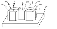
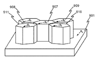
- FIGS. 10A to 10D are schematic views of a crystal made of a group III nitride semiconductor epitaxially grown in an c-axis orientation on an ⁇ -Al 2 O 3 (0001) substrate.
- reference numeral 901 denotes an ⁇ -Al 2 O 3 (0001) substrate
- reference numerals 902 to 911 denote a crystal made of a group III nitride semiconductor
- reference numeral cf denotes a c axis of a crystal made of a group III nitride semiconductor.
- c s is the orientation of the c-axis of the ⁇ -Al 2 O 3 (0001) substrate
- a f is the orientation of the a-axis of the crystal comprising a group III nitride semiconductor
- a s is ⁇ -Al 2 O 3 (0001 ) The orientation of the a-axis of the substrate.
- FIG. 10A is a bird's-eye view showing how a crystal made of a group III nitride semiconductor is formed with mosaic spread of a tilt
- FIG. 10B shows a cross-sectional structure of a part of the crystal. ing.
- the orientation c f of the c axis of the crystals 902, 903, and 904 made of a group III nitride semiconductor is substantially parallel to the orientation c s of the c axis of the substrate, and the substrate is dominant with respect to the whole.
- FIG. 10C is a bird's-eye view showing how a crystal made of a group III nitride semiconductor is formed with a mosaic spread of a twist
- FIG. 10D shows a top view thereof.
- the orientation a f of the a-axis of crystals 907, 908, 909 consisting of a group III nitride semiconductor forms an angle with the orientation a s of the a-axis of the ⁇ -Al 2 O 3 (0001) substrate. Is approximately 30 °, and the crystal orientation is dominant in the in-plane direction with respect to the whole, while the a-axis direction a f of the crystals 910 and 911 made of a group III nitride semiconductor is the above-mentioned It is formed slightly out of the crystal orientation in the in-plane direction.
- mosaic spread Such variation from the dominant crystal orientation to the whole is called mosaic spread, and in particular, variation in crystal orientation in the vertical direction of the substrate is mosaic spread in tilt, and variation in crystal orientation in the in-plane direction is twist mosaic.
- mosaic spread It is known that the mosaic spread of the tilt and twist is correlated with the density of defects such as screw dislocations and edge dislocations formed inside the group III nitride semiconductor thin film, and the mosaic of the tilt and twist is By reducing the spread, the density of the above defects is reduced, and a high quality group III nitride semiconductor thin film is easily obtained.
- the size of the mosaic spread of the tilt or twist is determined by XRC measurement on a specific lattice plane (symmetrical plane) formed parallel to the substrate surface or a specific lattice plane formed perpendicular to the substrate surface. It can be evaluated by examining the FWHM of the obtained diffraction peak.
- FIGS. 10A to 10D and the above description explain the mosaic spread of the tilt and the twist in an easy-to-understand manner conceptually and do not guarantee the strictness at all.
- the crystal orientation in the substrate vertical direction dominant to the whole or the crystal orientation in the in-plane direction dominant to the whole is not necessarily the c-axis or a of the ⁇ -Al 2 O 3 (0001) substrate. It may not completely match the orientation of the axis.
- the gap between crystals as shown in FIG. 10D may not necessarily be formed.
- the mosaic spread indicates the degree of variation from the dominant crystal orientation.
- group III nitride semiconductor thin films have growth modes of + c polarity and -c polarity as shown in FIG. 11, and epitaxial films with better quality of + c polarity growth than -c polarity growth It is known that it is easy to obtain. Therefore, in order to adopt the sputtering method as a film forming process of the group III nitride semiconductor thin film, it is desirable that an epitaxial film of + c polarity be obtained.
- + c polarity is a term which means Al polarity, Ga polarity, and In polarity regarding AlN, GaN, and InN, respectively.
- -c polarity is a term that means N polarity.
- Patent Document 1 plasma processing is performed on a substrate before forming a Group III nitride semiconductor thin film (AlN in Patent Document 1) on an ⁇ -Al 2 O 3 substrate using a sputtering method.
- a method of achieving high quality of a group III nitride semiconductor thin film, in particular, a method of obtaining a group III nitride semiconductor thin film with extremely small tilt mosaic spread is disclosed.
- a buffer layer (intermediate layer in Patent Document 2) formed of a Group III nitride semiconductor (in Patent Document 2, a Group III nitride compound) is formed on a substrate by sputtering.
- Group III nitride semiconductor in which an n-type semiconductor layer including an underlayer, a light emitting layer, and a p-type semiconductor layer are sequentially stacked on a buffer layer made of a group III nitride semiconductor (in Patent Document 2, a group III nitride compound semiconductor) A method of manufacturing a light emitting device is disclosed.
- Patent Document 2 as a procedure for forming a buffer layer composed of a group III nitride semiconductor, a pretreatment step of subjecting the substrate to plasma treatment, and a buffer composed of a group III nitride semiconductor by a sputtering method following the pretreatment step Forming a layer is described. Further, in Patent Document 2, an ⁇ -Al 2 O 3 substrate and AlN are used as a preferable form of the substrate and the buffer layer made of a group III nitride semiconductor, and an n-type semiconductor layer provided with a base film, a light emitting layer, The MOCVD method is preferably used as a method for forming the p-type semiconductor layer.
- Patent Document 1 can reduce the mosaic spread of the tilt and is a powerful technique, but to form a higher quality epitaxial film by using the sputtering method. There are still issues to be improved.
- the group III nitride semiconductor thin film obtained as a result of conducting the confirmation experiment of the technique disclosed in Patent Document 1 by the present inventors is obtained as an epitaxial film with less mosaic spread, but + c polarity and -c The polarity was mixed. Therefore, it is apparent that the technique disclosed in Patent Document 1 alone can not obtain a group III nitride semiconductor thin film of + c polarity.
- Patent Document 2 does not describe a method of controlling the polarity of a buffer layer made of a Group III nitride semiconductor film-formed using a sputtering method. Also in the result of the inventors of the present invention performing a confirmation experiment of the technology disclosed in Patent Document 2, the obtained light emitting element could not obtain good light emission characteristics.
- the buffer layer made of a Group III nitride semiconductor film-formed using a sputtering method has + c polarity and -c polarity. It was found that the epitaxial film was a mixture of More specifically, even if the n-type semiconductor layer, the light emitting layer, and the p-type semiconductor layer provided with the base film are sequentially stacked by the MOCVD method, the contralateral boundary caused by the mixture of polarities in the buffer layer made of group III nitride semiconductor Many defects are formed inside the device, which lowers the light emission characteristics. That is, it is apparent that the technique disclosed in Patent Document 2 alone can not obtain a group III nitride semiconductor thin film having + c polarity, and can not obtain a light emitting element having good light emission characteristics.
- the present inventors have found that when the Group III nitride semiconductor thin film fabricated using the sputtering method is an epitaxial film with mixed polarity, it is formed inside the device. It was concluded that the deterioration of the device characteristics due to defects such as the contralateral boundary was inevitable.
- an object of the present invention to provide an epitaxial film forming method capable of forming an + c-polar epitaxial film by sputtering, and a vacuum processing apparatus suitable for the epitaxial film forming method. It is an object of the present invention to provide a method of manufacturing a semiconductor light emitting device using this epitaxial film, and a semiconductor light emitting device and a lighting device manufactured by this manufacturing method.
- the present inventors completed the present invention as a result of earnest research, as described later, obtained new findings that the polarity of the epitaxial film depends on the method of placing the substrate on the substrate holder.
- the present invention provides an epitaxial film forming method for epitaxially growing a Group III nitride semiconductor thin film by sputtering on an ⁇ -Al 2 O 3 substrate heated to an arbitrary temperature using a heater a is, the ⁇ -Al 2 O 3 substrate, and the step of holding spaced by substrate-facing surface and a predetermined distance of the heater, in a state in which the predetermined distance is held apart, the alpha-Al 2 And forming an epitaxial film of a group III nitride semiconductor thin film on an O 3 substrate.
- the present invention includes a vacuum evacuable vacuum chamber, alpha-Al 2 and O 3 substrate holding means for supporting the substrate, said alpha-Al 2 O 3 substrate held by the substrate holding means any temperature using a vacuum processing apparatus provided with a heatable heater, an epitaxial film forming method of forming an epitaxial film of a group III nitride semiconductor thin film by sputtering on the ⁇ -Al 2 O 3 substrate, the substrate supporting the ⁇ -Al 2 O 3 substrate held by means, while holding spaced by substrate-facing surface and a predetermined distance of the heater, the ⁇ -Al 2 O 3 on a substrate a group III nitride semiconductor thin film An epitaxial film is formed.
- the present invention is a vacuum processing apparatus, comprising: a vacuum container capable of vacuum evacuation; substrate holding means for supporting a substrate; and a heater capable of heating the substrate held by the substrate holding means to an arbitrary temperature. And a target electrode provided in the vacuum vessel and to which a target can be attached, wherein the substrate holding means is provided on the lower side in the direction of gravity of the target electrode in the vacuum vessel, and the substrate is The heater may be separated from the substrate facing surface by a predetermined distance.
- the present invention it is possible to produce an epitaxial film of a group III nitride semiconductor of + c polarity with less mosaic spread of tilt and twist on an ⁇ -Al 2 O 3 substrate using a sputtering method.
- the group III nitride semiconductor epitaxial film manufactured by the sputtering method the light emission characteristics of the light emitting device such as the LED and the LD can be improved.
- the main features relating to the present invention are an ⁇ -Al 2 O 3 substrate heated by a heater when epitaxially growing a Group III nitride semiconductor thin film on an ⁇ -Al 2 O 3 substrate by a sputtering method such as a high frequency sputtering method. Forming a group III nitride semiconductor film while keeping a predetermined distance from the substrate facing surface of the heater.
- a sputtering method such as a high frequency sputtering method.
- FIGS. 1 to 9 are views of an LED structure manufactured using a vacuum processing apparatus (high frequency sputtering apparatus) or an epitaxial film formed as a film according to an embodiment of the present invention.
- 1 is a schematic cross-sectional view of a high frequency sputtering apparatus
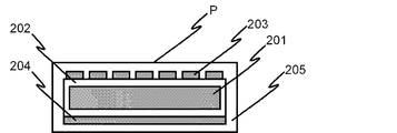
- FIG. 2 is a schematic cross-sectional view of a heater
- FIG. 3 is a schematic cross-sectional view of another heater
- FIGS. 4A and 4B are configuration examples of top views of heater electrodes
- FIG. 6 is a second structural example of the substrate holding apparatus
- FIG. 7 is a third structural example of the substrate holding apparatus
- FIG. 8 is an enlarged view of a supporting portion of the substrate holding apparatus
- FIG. 1 is an example of a cross-sectional view of an LED structure fabricated using a filmed epitaxial film.
- it has abbreviate
- FIG. 1 is a schematic block diagram of an example of a sputtering apparatus used for forming a group III nitride semiconductor thin film according to the present invention.
- numeral 101 is a vacuum vessel
- numeral 102 is a target electrode
- numeral 99 is a substrate holder
- numeral 103 is a heater
- numeral 503 is a substrate holding device
- numeral 105 is a target shield
- numeral 106 is a high frequency
- Reference numeral 107 is a substrate
- reference numeral 108 is a target
- reference numeral 109 is a gas introduction mechanism
- reference numeral 110 is an exhaust mechanism
- reference numeral 112 is a reflector
- reference numeral 113 is an insulating material
- reference numeral 114 is a chamber shield
- reference numeral 115 is a magnet unit
- reference numeral 116 Denotes a target shield holding mechanism
- reference numeral 203 denotes a heater electrode.
- reference numeral 550 denotes
- the vacuum vessel 101 is configured using a metal member such as stainless steel or an aluminum alloy and is electrically grounded. Further, the temperature rise of the wall surface of the vacuum vessel 101 is prevented or reduced by a cooling mechanism (not shown). Further, the vacuum vessel 101 is connected to the gas introduction mechanism 109 via a mass flow controller (not shown) and to the exhaust mechanism 110 via a variable conductance valve (not shown).
- the target shield 105 is attached to the vacuum vessel 101 via a target shield holding mechanism 116.
- the target shield holding mechanism 116 and the target shield 105 can be metal members such as stainless steel or aluminum alloy, and have the same potential as the vacuum vessel 101 in direct current.
- the target electrode 102 is attached to the vacuum vessel 101 via the insulating material 113.
- the target 108 is attached to the target electrode 102, and the target electrode 102 is connected to the high frequency power source 106 via a matching box (not shown).
- the target 108 may be attached directly to the target electrode 102 or may be attached to the target electrode 102 via a bonding plate (not shown) made of a metal member such as copper (Cu).
- the target 108 may be a metal target containing at least one of Al, Ga, or In, or a nitride target containing at least one of the group III elements.
- the target electrode 102 is provided with a cooling mechanism (not shown) for preventing the temperature rise of the target 108.
- a magnet unit 115 is incorporated in the target electrode 102.
- the high frequency power supply 106 13.56 MHz is industrially easy to use, but it is also possible to use other frequencies, superimpose a direct current on a high frequency, or use them in pulses.
- the chamber shield 114 is attached to the vacuum vessel 101 to prevent adhesion of a film to the vacuum vessel 101 at the time of film formation.
- the substrate holder 99 has a heater 103, a substrate holding device 503, and a reflector 112 as main components.
- the heater 103 incorporates a heater electrode 203.
- the substrate holding device 503 has at least a portion in contact with the substrate as an insulating member, and is fixed by the reflector 112 or a shaft (not shown). By holding the substrate 107 in the substrate holding device 503, it can be disposed with a predetermined gap from the substrate facing surface P of the heater 103. A detailed example of the substrate holding device 503 will be described later.
- the target electrode 102 capable of disposing a target above the gravity direction is disposed, and the substrate holder 99 is disposed below the target electrode 102 in the gravity direction. It is arranged. Therefore, since the substrate 107 can be held by the substrate holding device 503 using gravity, it is possible to mount the substrate 107 only by mounting the substrate 107 on a substrate support portion (such as reference numeral 503a described later) of the substrate holding device 503. The entire surface can be exposed to the side of the target 108, and an epitaxial film can be formed on the entire surface of the substrate 107.
- a substrate support portion such as reference numeral 503a described later
- the target electrode 102 is disposed above the vacuum chamber 101 in the direction of gravity, and the substrate holder 99 is disposed below the target electrode 102 in the direction of gravity.
- the substrate holder 99 may be disposed on the upper side in the direction, and the target electrode 102 may be disposed on the lower side in the gravity direction than the substrate holder 99.
- FIG. 2 or 3 shows an example of the structure of the heater 103.
- reference numeral 201 denotes a base
- reference numeral 202 denotes a base coat
- reference numeral 203 denotes a heater electrode
- reference numeral 204 denotes a back side coat
- reference numeral 205 denotes an overcoat.
- symbol P is an upper surface (board
- the base 201 is graphite
- the heater electrode 203 and the back side coat 204 are pyrolytic graphite (PG)
- the base coat 202 and the overcoat 205 are pyrolytic boron nitride (PBN).
- the base coat 202 and overcoat 205 made of PBN are high-resistance materials.
- the heater 103 can emit infrared light of a predetermined wavelength band, and can heat the substrate to an arbitrary temperature.
- FIG. 3 shows another example of the configuration of the heater.
- Reference numeral 301 denotes a base
- reference numeral 302 denotes a heater electrode
- reference numeral 303 denotes a back side coat
- reference numeral 304 denotes an overcoat.
- the base 301 is boron nitride (BN)
- the heater electrode 302 and the back side coat 303 are PG
- the overcoat 304 is PBN.
- the base 301 made of BN and the overcoat 304 made of PBN are high-resistance materials.
- the material constituting the heaters, the efficiency of heating the ⁇ -Al 2 O 3 substrate as compared to conventional infrared lamp is preferably used for high, ⁇ -Al 2 O 3 substrate a predetermined temperature It is not limited to this as long as it can be heated.
- the structural example (top view) of the heater electrode 203 (or 302) is shown to FIG. 4A and 4B.
- the heater electrode 203 (or 302) incorporated in the heater 103 has an electrode pattern as shown in FIGS. 4A and 4B.
- a power source (not shown) is connected to this electrode pattern, and a DC or AC voltage is applied, whereby a current flows through the heater electrode 203 (or 302), and the generated Joule heat heats the heater 103.
- the substrate is heated by infrared rays emitted from the heater 103.
- an electrode pattern is not limited to FIG. 4A and 4B.
- heat can be uniformly applied to the entire surface of the substrate 107. Therefore, it is desirable to use an electrode pattern such that the heat acts on the entire surface of the substrate as uniformly as possible.
- it is important to be able to form an epitaxial film of + c polarity even when using an electrode pattern that causes heat to uniformly act on the substrate. What shape is the electrode pattern itself? Is not the essence. Therefore, in the present embodiment, without being limited to the electrode patterns shown in FIGS. 4A and 4B, it goes without saying that any electrode pattern can be applied to the present embodiment.
- the heater 103 may have a structure in which the heater 103 shown in FIG. 2 or 3 is inverted, that is, a face opposite to the face indicated by reference symbol P in FIGS.
- the substrate is heated via the back side coat 204 or 303, the power efficiency of the substrate heating is lowered, but the back side coat 204 or 303 plays a role of soaking, and is uniform to the substrate. Has the effect of causing heat to
- FIG. 5 is a cross-sectional view of a heater and a substrate holding device (first configuration example).
- reference numeral 103 denotes a heater
- reference numeral 203 denotes a heater electrode
- reference numeral 503 denotes a substrate holding device
- reference numeral 504 denotes a substrate (the holder support portion 550 is not shown).
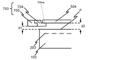
- the substrate holding device 503 is a substantially ring-shaped member having the same cross section, and is provided with a substrate supporting portion 503a made of an insulating member for supporting the outer edge portion of the substrate from below (the gravity direction lower side, ie, the heater 103 side). ing.
- the substrate supporting portion 503 a is disposed between the substrate facing surface P of the heater 103 and a gap d 1. Further, a gap d 2 is provided between the substrate 504 and the substrate facing surface P of the heater 103. Thus, when the substrate 504 is supported by the substrate support 503 a, the substrate support is arranged such that the substrate 504 is disposed with a predetermined gap (for example, d 2) from the substrate facing surface P of the heater 103. 503a is provided. As a clearance of d1, 0.4 mm or more is desirable, and 0.5 mm or more is preferably used as a clearance of d2.
- the gap d1 is less than 0.4 mm, a mixed group III nitride semiconductor thin film is easily formed on the outer peripheral portion, and if the gap d2 is less than 0.5 mm, a mixed group III nitride is mixed on the entire surface of the substrate It is not preferable because the semiconductor semiconductor thin film is easily formed.
- a gap d1 of 0.4 mm or more is provided between the lower side surface of the substrate holding device 503 and the substrate facing surface P of the heater 103.
- a gap d2 of 0.5 mm or more is provided between the substrate 504 and the substrate facing surface P of the heater 103.
- the heating efficiency of the substrate 504 by the heater 103 is lowered, so it is not preferable to make the d1 and d2 too wide. If d1 and d2, especially d2 are too wide, plasma may be generated in the space between the heater 103 and the substrate 504, and the effects of the present invention may be lost. Desirably, 2 mm or less is desirable.
- FIG. 6 shows a second configuration example of the substrate holding device.
- reference numeral 504 denotes a substrate
- reference numeral 603 denotes a substrate holding device (the holder support portion 550 is not shown).
- the substrate holding device 603 is a substantially ring-shaped member having the same cross section, and a substrate support portion 603a formed of an insulating member for holding the substrate 504 from below and a mounting integrally formed on the outer periphery of the substrate support portion 603a. And a holder 603b.
- a gap d 1 is provided between the back side of the substrate support portion 603 a (the side facing the heater 103) and the substrate facing surface P of the heater 103.
- a gap d2 is provided between the substrate 504 and the substrate facing surface P of the heater 103, respectively.
- the gap d1 is preferably 0.4 mm or more, and the gap d2 is preferably 0.5 mm or more.
- FIG. 7 shows a third configuration example of the substrate holding device.
- reference numeral 504 denotes a substrate
- reference numeral 703 denotes a substrate holding device.
- the substrate holding device 703 is a substantially ring-shaped member having the same cross section, and includes a first substrate holding device 704 and a second substrate holding device 705.
- the second substrate holding device 705 is formed of a conductive ring, and is connected to a high frequency power supply (not shown) via a matching box (not shown). Therefore, by supplying high frequency power to the second substrate holding device 705 in an atmosphere containing a gas such as N 2 or a rare gas, plasma can be generated in the vicinity of the substrate to perform surface treatment of the substrate. It is.
- a gas such as N 2 or a rare gas
- the first substrate holding device 704 is provided with a substrate support portion 704 a made of an insulating member for supporting the substrate 504 from the lower side.
- a gap d1 is provided between the back side of the substrate support portion 704a and the substrate facing surface P of the heater 103, and a gap d2 is provided between the substrate 504 and the substrate facing surface P of the heater 103.
- the holder support portion 750 has a structure for supporting the second substrate holding device 705, and includes a conductive material 751, an insulating material 753, and a stainless steel pipe 755 as main components.
- the conductive material 751 is electrically connected to a high frequency power supply 757 and a second substrate holding device 705 provided outside the vacuum vessel 101. Therefore, high frequency power is supplied to the second substrate holding device 705 from the high frequency power supply 757 through the conductive material 751.
- the conductive material 751 is covered with an insulating material 753 and a stainless steel pipe 755. Further, insulation between the conductive material 751 and the vacuum vessel 101 is also ensured by the insulating material 753.
- the holder support 750 is configured to support the second substrate holder 705 and to supply power to the second substrate holder 705.
- the holder support portion 750 shown in FIG. 8 is configured to have a conductive material 751 for supplying high frequency power to the second substrate holding device 705. However, the holder support for supporting the substrate holding devices 503 and 603 The conductive material 751 is not necessary in the portion 550 (see FIG. 1).
- the substrate supporting portions 503a, 603a and 704a are not ring-shaped. It is good.
- the substrate supporting portions 503a, 603a, and 704a may be plate-like insulating members in which the opening is not formed.
- the substrate support portion is disposed with a predetermined gap (for example, d1) from the heater 103.
- a predetermined gap for example, d1
- the substrate 107 is exposed to the heater 103 while disposing the substrate 107 and the substrate facing surface P of the heater 103 with a predetermined gap. be able to. Therefore, since the substrate 107 can be efficiently heated, it is preferable to make the substrate support in a ring shape.
- an insulating member used for the substrate support portions 503a, 603a, and 704a for example, quartz, sapphire, alumina, or the like can be used.
- the structure of the heater 103 may be any structure shown in FIG. 2 or FIG. 3 or may be an inverted structure, and in this embodiment, the heater structure is not essential, and the heater of other structure is used. May be used.
- the heater electrode may have a structure of a heater disposed so as to be exposed to the substrate facing surface P of the heater.
- the structures of the substrate holding devices 503, 603, and 703 may use any of the structures shown in FIGS. 5, 6, and 7 or substrate holding devices having other structures. What is important in the present embodiment is that, in the film formation of the group III nitride semiconductor thin film, the substrate is disposed at a predetermined distance from the substrate facing surface P of the heater.
- the space between the substrate facing surface P of the heater and the substrate is a gap, but it is considered that the same effect can be obtained even if the gap is filled with the insulating member. Therefore, as long as the substrate can be disposed apart from the substrate facing surface P of the heater by a predetermined distance, the substrate holding device is not limited to FIGS. 5 to 7, and any structure may be used. For example, in the case of an apparatus having a mechanism for transferring a substrate by raising and lowering a lift pin, the substrate may be held at a position having a predetermined gap from the substrate facing surface P of the heater 103 using the lift pin.
- the film wraps around the gap between the outer periphery of the substrate and the heater 103, and the film adheres to the substrate facing surface P of the heater 103, and the radiation from the heater 103 changes with time. Is the preferred form.
- plasma is generated in the vicinity of the substrate using a high frequency power supply 757 connected to the second substrate holding device 705 (third configuration example) shown in FIG. To remove components such as moisture and hydrocarbons adhering to the substrate surface.
- a high frequency power supply 757 connected to the second substrate holding device 705 (third configuration example) shown in FIG.
- the structure of the heater electrode either of the patterns shown in FIGS. 4A and 4B may be used, or patterns of other structures as described above may be used.
- the structure of FIG. 6 is preferably used because the gaps d1 and d2 between the heater 103 and the substrate facing surface P can be easily controlled more accurately than the structure of FIG. Further, by using the structure of FIG. 7, it is possible to remove components such as moisture and hydrocarbons adhering to the substrate surface, and reproducibility of the crystallinity of the Group III nitride semiconductor thin film is improved. .
- FIG. 9 is an example of a cross-sectional structure of a light emitting diode (LED) as a semiconductor light emitting device manufactured using the method for manufacturing a group III nitride semiconductor thin film according to the present invention.
- reference numeral 801 denotes an ⁇ -Al 2 O 3 substrate
- 802 denotes a buffer layer
- 803 denotes a III nitride semiconductor intermediate layer
- 804 denotes an n-type III nitride semiconductor layer
- 805 denotes III nitride
- reference numeral 806 is a p-type group III nitride semiconductor layer
- reference numeral 807 is an n-type electrode
- reference numeral 808 is a p-type bonding pad electrode
- reference numeral 809 is a protective layer
- reference numeral 810 is a light transmitting electrode.
- the buffer layer 802 As a material for forming the buffer layer 802, AlN, AlGaN, or GaN is preferably used.
- Materials constituting the group III nitride semiconductor intermediate layer 803, the n-type group III nitride semiconductor layer 804, the group III nitride semiconductor active layer 805, and the p-type group III nitride semiconductor layer 806 include AlGaN, GaN and InGaN. It is preferably used.
- the n-type Group III nitride semiconductor layer 804 contains silicon (Si) or germanium (Ge) in the above material, and the p-type III group nitride semiconductor layer 806 contains magnesium (Mg) or zinc (Zn) in the above material.
- a lighting device can be configured using the light emitting diode (LED) described above.
- the epitaxial film is formed on the ⁇ -Al 2 O 3 substrate by the method including the following first to fourth steps.
- the substrate 107 is introduced into the vacuum vessel 101 held at a predetermined pressure by the exhaust mechanism 110.
- the substrate ( ⁇ -Al 2 O 3 substrate) 107 is transported by the transport robot (not shown) to the top of the heater 103 and placed on the top of the lift pins (not shown) protruding from the heater 103.
- the lift pins holding the substrate 107 are lowered, and the substrate 107 is placed on the substrate holding device 503.
- the voltage applied to the heater electrode 203 incorporated in the heater 103 is controlled to keep the substrate 107 at a predetermined temperature.
- the temperature of the heater 103 is monitored by using a thermocouple (not shown) built in the heater 103, or the temperature of the heater 103 is monitored by using a pyrometer (not shown) installed in the vacuum vessel 101. Is controlled so as to be a predetermined temperature.
- one of N 2 gas, a rare gas, and a mixed gas of N 2 gas and a rare gas is introduced into the vacuum vessel 101 from the gas introduction mechanism 109, and a mass flow controller (not shown) and variable conductance
- the pressure of the vacuum vessel 101 is set to a predetermined pressure by a valve (not shown).
- high frequency power is applied from the high frequency power source 106 to generate high frequency plasma on the front surface of the target 108, and ions in the plasma strike out elements constituting the target 108, thereby obtaining a group III nitride semiconductor Deposit a thin film.
- a metal target is used as the target 108
- N 2 gas or a mixed gas of N 2 gas and a rare gas is preferably used as a process gas, and the surface of the target 108, the surface of the substrate 107, and the target 108 and the substrate 107.
- the group III element constituting the metal target is nitrided in at least one region of the space between them, and a group III nitride semiconductor thin film is formed on the substrate.
- any of N 2 gas, a rare gas, and a mixed gas of N 2 gas and a rare gas is preferably used, and sputtered particles in the form of atoms or nitride molecules from the surface of the target Is released.
- the Group III element released as atoms from the target surface is nitrided in at least one region of the surface of the target 108, the surface of the substrate 107, and the space between the target 108 and the substrate 107, and the Group III nitride on the substrate A semiconductor thin film is formed.
- most of the nitride molecules released from the target surface reach the substrate to form a group III nitride semiconductor thin film.
- the group III element generated by the dissociation is the substrate 107.
- the nitride film is again nitrided to form a group III nitride semiconductor thin film on any one of the surface of the substrate 108 and the space between the target 108 and the substrate 107.
- the predetermined pressure in the first step is desirably less than 5 ⁇ 10 -4 Pa, and above that, impurities such as oxygen are taken into the inside of the Group III nitride semiconductor thin film, and a good epitaxial film is obtained. It is hard to be Further, the temperature of the heater 103 in the first step is not particularly limited, but from the viewpoint of productivity, it is desirable to set the temperature for obtaining the substrate temperature at the time of film formation.
- the predetermined temperature in the second step is set to the film forming temperature in the fourth step
- the predetermined pressure in the third step is the pressure in the fourth step. It is desirable from the viewpoint of productivity to set to the membrane pressure.
- the second step and the third step may be performed at different timings, or may be performed simultaneously. Moreover, it is desirable from the viewpoint of productivity that the temperature set in the second step and the pressure set in the third step are maintained at least until the fourth step is started.
- the substrate temperature at the time of performing the fourth step is desirably set in the range of 100 to 1200 ° C., and more preferably in the range of 400 to 1000 ° C. If the temperature is less than 100 ° C., a film having a mixture of amorphous structures is easily formed, and if the temperature is higher than 1200 ° C., the film itself is not formed or an epitaxial film having many defects due to thermal stress is obtained even if formed. Cheap.
- the deposition pressure is preferably set in the range of 0.1 to 100 mTorr (1.33 ⁇ 10 -2 to 1.33 ⁇ 10 1 Pa), and further, 1.0 to 10 mTorr (1.33 ⁇ ). It is preferable to set in the range of 10 ⁇ 1 to 1.33 Pa).
- the fourth step it is also possible to temporarily increase the pressure of the vacuum vessel 101 above the film forming pressure to promote the generation of plasma.
- the film formation pressure may be increased by temporarily introducing a large amount of at least one kind of process gas flow rate temporarily, and the opening degree of the variable conductance valve (not shown) may be temporarily reduced.
- the deposition pressure may be increased.
- the substrate 107 may be transported to a pretreatment chamber (not shown), and the substrate may be subjected to heat treatment or plasma treatment at a temperature higher than the film formation temperature.
- a pretreatment chamber not shown
- the substrate may be subjected to heat treatment or plasma treatment at a temperature higher than the film formation temperature.
- the nitride semiconductor active layer 805 and the p-type group III nitride semiconductor layer 806 can be mentioned. All the layers described above may be manufactured using the sputtering apparatus (epitaxial film forming method) according to the present invention, or the sputtering apparatus (epitaxial film forming method) according to the present invention may be limited to any layer. It may be produced.
- the buffer layer 802 is manufactured using the sputtering apparatus (epitaxial film forming method) according to the present invention, and thereafter the group III nitride semiconductor is manufactured using the MOCVD method.
- the group III nitride semiconductor is manufactured using the MOCVD method.
- the buffer layer 802 and the group III nitride semiconductor intermediate layer 803 are manufactured using the sputtering apparatus (epitaxial film forming method) according to the present invention, and then the n-type III is manufactured using the MOCVD method.
- the sputtering apparatus epipitaxial film forming method
- MOCVD method MOCVD method
- the buffer layer 802, the group III nitride semiconductor intermediate layer 803, and the n-type group III nitride semiconductor layer 804 are manufactured using the sputtering apparatus (epitaxial film forming method) according to the present invention, and There is a method of manufacturing an epitaxial wafer by sequentially laminating the group III nitride semiconductor active layer 805 and the p-type group III nitride semiconductor layer 806 using the MOCVD method.
- a sputtering apparatus is used as a buffer layer 802, a group III nitride semiconductor intermediate layer 803, an n-type group III nitride semiconductor layer 804 and a group III nitride semiconductor active layer 805 (epitaxial film forming method).
- a method of fabricating an epitaxial wafer by fabricating the p-type Group III nitride semiconductor layer 806 by using the MOCVD method.
- a buffer layer 802, a group III nitride semiconductor intermediate layer 803, an n-type group III nitride semiconductor layer 804 and a group III nitride semiconductor active layer 805, and a p-type group III nitride semiconductor layer 806 are used.
- the epitaxial wafer thus obtained is subjected to lithography technology and RIE (reactive ion etching) technology, and as shown in FIG. 9, a translucent electrode 810, a p-type bonding pad electrode 808, an n-type electrode 807, protection By forming the film 809, an LED structure can be obtained.
- the materials of the light-transmissive electrode 810, the p-type bonding pad electrode 808, the n-type electrode 807, and the protective film 809 are not particularly limited, and materials well known in this technical field can be used without limitation.
- an example in which an AlN film is formed on an ⁇ -Al 2 O 3 (0001) substrate using the film forming method of a group III nitride semiconductor thin film according to the present invention more specifically, An example in which an AlN film is formed on an ⁇ -Al 2 O 3 (0001) substrate mounted with a gap from the substrate facing surface of a heater by a substrate holding device using a sputtering method will be described.
- the AlN film is formed using the same sputtering apparatus as that of FIG. 1, the structure of the heater is as shown in FIG. 2, the pattern of the heater electrode is as shown in FIG. 4A, and the substrate holding device is the same as FIG. Using.
- the gap d1 between the substrate supporting portion 503a and the substrate facing surface P of the heater 103 and the gap d2 between the substrate 504 and the substrate facing surface P of the heater 103 in FIG. 5 are 1 mm and 2 mm, respectively.
- the ⁇ -Al 2 O 3 (0001) substrate is transported to the vacuum vessel 101 held at 1 ⁇ 10 ⁇ 4 Pa or less in the first step and disposed in the substrate holding device 503,
- the substrate was maintained at 550 ° C., which is the film formation temperature in the fourth step.
- the heater 103 was controlled so that the monitor value of the built-in thermocouple became 750.degree.
- a mixed gas of N 2 and Ar is introduced such that N 2 / (N 2 + Ar): 25%, and the pressure of the vacuum vessel 101 is the film forming pressure in the fourth step. It was set to 3.75 mTorr (0.5 Pa).
- a high frequency power of 2000 W is applied from the high frequency power source 106 to the target 108 made of metal Al from the high frequency power source 106 in the fourth step, and an AlN film with a film thickness of 50 nm is formed on the substrate by sputtering.
- the deposition temperature in this embodiment is embedded thermocouple performed beforehand substrate temperature measured by ⁇ -Al 2 O 3 (0001 ) substrate, at that time, ⁇ -Al 2 O 3 (0001 ) and the temperature of the substrate
- the monitor value of the thermocouple built in the heater, that is, the relationship is set in relation to the temperature of the heater.
- the produced AlN film was subjected to X-ray diffraction (XRD) measurement of 2 ⁇ / ⁇ scan mode at the symmetrical reflection position, XRC measurement at ⁇ scan mode with respect to the symmetry plane, and ⁇ scan at In-plane arrangement. Evaluation was performed by XRC measurement of the mode and measurement of coaxial impact collision scattering (CAICISS).
- XRD X-ray diffraction
- CAICISS coaxial impact collision scattering
- XRC measurement in the ⁇ scan mode with respect to the plane of symmetry was performed on the AlN film manufactured in this example.
- the AlN (0002) plane was used for the measurement.
- the FWHM of the obtained XRC profile is 450 arcsec or less when the detector is in the open detector state, 100 arcsec or less when the analyzer crystal is inserted in the detector, and the mosaic spread of the tilt in the produced AlN film is very high. I confirmed that it was small.
- the XRC measurement when an analyzer crystal is inserted in the detector one having an FWHM of 20 arcsec or less is obtained.
- the original XRC measurement is performed when the detector is in the open detector state
- the FWHM of the XRC profile is broadened by the film thickness effect and lattice relaxation. It will be difficult to assess the mosaic spread correctly. Therefore, in recent years, as described above, when an analyzer crystal is inserted in the detector, it is also treated as a broad XRC measurement.
- the open detector state is used unless otherwise specified.
- the a-axis of the AlN film is 30 ° to the a-axis of the ⁇ -Al 2 O 3 (0001) substrate. I was able to confirm that it was rotating inside. This indicates that the AlN film is formed in a general epitaxial relationship when epitaxially growing the AlN film on the ⁇ -Al 2 O 3 (0001) substrate.
- FIG. 12 shows the results of CAICISS measurement on the AlN film produced in this example.
- the Al signal is detected by changing the incident angle from the AlN [11-20] orientation, and it can be seen that the peak at an incident angle of around 70 ° is obtained as a single shape. This indicates that the obtained AlN film has + c polarity (Al polarity).
- the AlN film produced in this example is a c-axis oriented epitaxial film having + c polarity (Al polarity) and an extremely small tilt mosaic spread. That is, according to the present invention, it has been clarified that a group III nitride semiconductor thin film of + c polarity can be obtained while reducing mosaic spread of tilt and twist.
- the target electrode 102 for holding the target is disposed on the upper side in the direction of gravity, and the substrate holder 99 is disposed on the lower side in the direction of gravity.
- a support member for example, a support claw
- the entire surface of the deposition surface of the substrate 107 can be exposed to the target 108. Therefore, according to the present embodiment, the mosaic spread of the tilt and the twist can be suppressed and the uniform group III nitride semiconductor thin film of + c polarity can be formed on the entire surface of the film formation surface of the substrate 107.
- an AlN film prepared using the film forming method of a group III nitride semiconductor thin film according to the present invention is used as a buffer layer, and undoped thereon using MOCVD.
- MOCVD Metal Organic Chemical Vapor Deposition
- An AlN film is formed on an ⁇ -Al 2 O 3 (0001) substrate under the same conditions as in the first embodiment by using a sputtering method, and then a wafer is introduced into a MOCVD apparatus to form a 5 ⁇ m thick undoped film. A GaN film was formed.
- the surface of the obtained undoped GaN film was a mirror surface, and the XRD measurement of 2 ⁇ / ⁇ scan mode at the symmetric reflection position showed that the undoped GaN film was c-axis oriented.
- each FWHM is It was confirmed that it was 250 arcsec or less and 500 arcsec or less. From this, it is understood that the obtained undoped GaN film is obtained as a high quality crystal with a small tilt and twist mosaic spread.
- the polarity of the obtained undoped GaN film was + c polarity (Ga polarity). This is because, as described in the first embodiment, the polarity of the AlN film used as the buffer layer can be controlled to the + c polarity, so it can be considered that the undoped GaN film formed thereon is also inherited its polarity. be able to.
- the AlN film controlled to + c polarity as the buffer layer manufactured by using the film forming method of the group III nitride semiconductor thin film according to the present invention, it is grown using the MOCVD method thereon.
- the obtained undoped GaN film can be obtained as a high quality epitaxial film controlled to + c polarity with less mosaic spread. That is, the group III nitride semiconductor thin film of + c polarity can be epitaxially grown on the ⁇ -Al 2 O 3 substrate.
- the undoped GaN film is formed by the MOCVD method in this embodiment, it is confirmed that the same result can be obtained by using the sputtering method.
- an AlN film prepared by using the method of forming a Group III nitride semiconductor thin film according to the present invention is used as a buffer layer, and on top of this, it is made of undoped GaN using MOCVD.
- III-nitride semiconductor intermediate layer n-type III-nitride semiconductor layer composed of Si-doped GaN, III-nitride semiconductor active layer having MQW structure of InGaN and GaN, p-type III-nitride semiconductor composed of Mg-doped GaN
- a layer is epitaxially grown in order, and further, an n-type electrode layer, a translucent electrode, a p-type electrode layer, and a protective film are formed, and then the wafer is separated by scribing to fabricate an LED element.
- An AlN film is formed on an ⁇ -Al 2 O 3 (0001) substrate under the same conditions as in the first embodiment by using a sputtering method, and then a wafer is introduced into a MOCVD apparatus to form a 5 ⁇ m thick undoped film.
- Group III nitride semiconductor intermediate layer consisting of GaN
- n-type group III nitride semiconductor layer consisting of Si-doped GaN with a film thickness of 2 ⁇ m
- stacked structure starting with GaN and ending with GaN, with 5 layers of 3 nm thickness
- a group III nitride semiconductor active layer having an MQW structure in which InGaN and six layers of GaN having a thickness of 16 nm are alternately stacked, and a p-type group III nitride semiconductor layer made of Mg doped GaN having a thickness of 200 nm .
- a light transmitting electrode 810, a p-type bonding pad electrode 808, an n-type electrode 807, and a protective film 809 were formed on the obtained epitaxial wafer using lithography and RIE as shown in FIG.
- ITO Indium-Tin-Oxide
- Ti titanium
- Al gold
- Au gold
- Ni nickel
- the wafer on which the LED structure thus obtained is formed is separated into 350 ⁇ m square LED chips by scribing, and the LED chips are mounted on a lead frame and connected to the lead frame with gold wires to connect with the LED elements did.
- an LED element having good light emission characteristics can be obtained by using an AlN film controlled to + c polarity as a buffer layer, which is manufactured using the film forming method of a group III nitride semiconductor thin film according to the present invention. I was able to get it.
- the p-type Group III nitride semiconductor layer made of doped GaN is formed by the MOCVD method, it has been confirmed that similar results can be obtained even if these layers are manufactured using the sputtering method.
- First comparative example As a first comparative example of the present invention, an AlN film was sputtered on an ⁇ -Al 2 O 3 (0001) substrate placed in contact with a heater without using the substrate holding device characteristic of the present invention. An example formed will be described.
- the AlN film is the same sputtering apparatus as the first embodiment except for the mounting method (arranging the ⁇ -Al 2 O 3 (0001) substrate with a gap from the heater), A film was formed using a heater and a heater electrode. Also, the film forming conditions for the AlN film were the same as in the first example.
- a buffer layer made of AlN is formed on an ⁇ -Al 2 O 3 (0001) substrate placed in contact with a heater using a sputtering method, and the buffer layer is formed thereon.
- An example in which the undoped GaN film is formed by using the MOCVD method will be described.
- the buffer layer made of AlN is deposited under the same sputtering apparatus, heater, heater electrode, and film forming conditions as in the first comparative example, and the undoped GaN film is the second embodiment and the second embodiment. Film formation was performed under the same conditions.
- a buffer layer made of AlN is formed on an ⁇ -Al 2 O 3 (0001) substrate by sputtering using the same sputtering apparatus, heater, heater electrode and film forming conditions as in the first comparative example. Thereafter, the wafer was introduced into the MOCVD apparatus to form an undoped GaN film having a thickness of 5 ⁇ m.
- the surface of the obtained undoped GaN film was cloudy, and the XRD measurement of 2 ⁇ / ⁇ scan mode at the symmetrical reflection position showed that the undoped GaN film was c-axis oriented.
- XRC measurement in ⁇ scan mode using GaN (0002) plane as the symmetry plane and XRC measurement in ⁇ scan mode for GaN ⁇ 10-10 ⁇ plane in In-plane configuration were performed. It was confirmed that the FWHM was about 360 arcsec and about 1000 arcsec. From this, it is obtained that the undoped GaN film obtained by the present comparative example is obtained as a low-quality crystal having a larger mosaic spread of tilt and twist as compared with the undoped GaN film obtained by the second embodiment. all right.
- the obtained undoped GaN film had a mixed film of + c polarity (Ga polarity) and -c polarity (N polarity).
- the buffer layer made of AlN is a film in which + c polarity and -c polarity are mixed, and therefore the undoped GaN film formed thereon is also mixed in polarity It can be considered as the result of taking over.
- the undoped GaN film grown thereon using the MOCVD method Is obtained as a low quality epitaxial film.
- the undoped GaN film is formed by the MOCVD method in the present comparative example, it is confirmed that the same result can be obtained by using the sputtering method.
- a buffer layer made of AlN is formed by a sputtering method in which an ⁇ -Al 2 O 3 (0001) substrate is placed in contact with a heater, and an MOCVD method is used thereon.
- Group III nitride semiconductor interlayer consisting of undoped GaN, n-type group III nitride semiconductor layer consisting of Si-doped GaN, Group III nitride semiconductor active layer having MQW structure of InGaN and GaN, p-type consisting of Mg-doped GaN
- a group III nitride semiconductor layer is epitaxially grown sequentially and further an n-type electrode layer, a light transmitting electrode, a p-type electrode layer and a protective film are formed, and then the wafer is separated by scribing .
- the method of forming the buffer layer made of AlN is the same as that of the first comparative example, and the group III nitride semiconductor intermediate layer made of undoped GaN and the n-type III made of Si-doped GaN are formed using MOCVD.
- the p-type electrode layer, the material of the protective film, the film formation method, and the subsequent steps of element formation are all the same as in the third embodiment.
- the p-type Group III nitride semiconductor layer made of doped GaN is formed by the MOCVD method, it is confirmed that the same result is obtained even if the sputtering method is used.
- a major feature of the present invention lies in the method of placing the substrate in order to form the epitaxial film of the group III nitride semiconductor of + c polarity on the ⁇ -Al 2 O 3 substrate.
- the substrate In order to obtain a uniform + c-polar epitaxial film, it is necessary to make specific relationship between the position of the substrate held by the substrate holder and the positional relationship between the heater provided in the substrate holder and the substrate holder. It is a technical thought that has not existed before.
- a substrate holding device for disposing the substrate at a predetermined distance from the substrate facing surface of the heater is provided on the substrate holder under the technical concept specific to the present invention.
- the substrate is separated from the substrate facing surface of the heater.
- the tray may be used to introduce the substrate, and the tray on which the substrate is placed under the concept of the present invention
- the substrate and the tray on which the substrate is placed may be placed apart from the heater by a predetermined distance.
- the substrate may be introduced using the substrate holding devices 503 and 603 or the substrate support unit 704 as a tray.
Landscapes
- Chemical & Material Sciences (AREA)
- Organic Chemistry (AREA)
- Engineering & Computer Science (AREA)
- Materials Engineering (AREA)
- Metallurgy (AREA)
- Crystallography & Structural Chemistry (AREA)
- Mechanical Engineering (AREA)
- Chemical Kinetics & Catalysis (AREA)
- Inorganic Chemistry (AREA)
- General Chemical & Material Sciences (AREA)
- Physical Deposition Of Substances That Are Components Of Semiconductor Devices (AREA)
- Led Devices (AREA)
- Physical Vapour Deposition (AREA)
- Crystals, And After-Treatments Of Crystals (AREA)
Abstract
Description
なお、チルトやツイストのモザイク広がりの大きさは、基板表面に平行に形成された特定の格子面(対称面)や、基板表面に垂直に形成された特定の格子面に対してXRC測定を行い、得られた回折ピークのFWHMを調べることで評価することができる。
すなわち、特許文献2には、スパッタリング法を用いて成膜したIII族窒化物半導体からなる緩衝層について、極性の制御方法が記載されていない。本発明者らが、特許文献2に開示された技術の確認実験を行なった結果においても、得られた発光素子では良好な発光特性を得ることができなかった。
本発明に関する主な特徴は、α-Al2O3基板上に、例えば高周波スパッタリング法といったスパッタリング法によりIII族窒化物半導体薄膜をエピタキシャル成長させる際に、ヒーターにより加熱されたα-Al2O3基板をヒーターの基板対向面から所定距離だけ離間して保持しながら、III族窒化物半導体の成膜を行うことにある。以下、図面を参照して本発明を説明する。なお、以下に説明する部材、配置等は発明を具体化した一例であって本発明を限定するものではなく、本発明の趣旨に沿って各種改変できることは勿論である。
ヒーター103に内蔵されたヒーター電極203(または302)は図4A、4Bのような電極パターンを有している。この電極パターンに電源(不図示)を接続し、直流または交流の電圧を印加することで、ヒーター電極203(または302)に電流が流れ、発生したジュール熱によりヒーター103が加熱される。基板はヒーター103から放射される赤外線により加熱される。
図6は、基板保持装置の第二の構成例を示している。図6において、符号504は基板、符号603は基板保持装置である(ホルダー支持部550は不図示)。基板保持装置603は、同一断面を有する略リング状の部材であり、下方から基板504を保持するための絶縁部材からなる基板支持部603aと、基板支持部603aの外周に一体に構成された載置部603bとを備えている。載置部603bがヒーター103の基板対向面Pに載置された状態では、基板支持部603aの裏側(ヒーター103と対向する側)とヒーター103の基板対向面Pとの間には隙間d1が、基板504とヒーター103の基板対向面Pとの間には隙間d2がそれぞれ設けられる。隙間d1としては、0.4mm以上が望ましく、隙間d2としては、0.5mm以上が望ましい。
図8は基板保持装置703の支持部(ホルダー支持部750)の拡大図である。ホルダー支持部750は、第二の基板保持装置705を支持する構造であり、導電材751、絶縁材753、およびステンレスパイプ755を主要な構成要素としている。導電材751は、真空容器101の外側に設けられた高周波電源757および第二の基板保持装置705に電気的に接続されている。よって、第二の基板保持装置705には導電材751を介して高周波電源757から高周波電力が供給される。導電材751は絶縁材753とステンレスパイプ755とで覆われている。また、導電材751と真空容器101との絶縁も絶縁材753によって確保している。このように、ホルダー支持部750は、第二の基板保持装置705を支持すると共に、該第二の基板保持装置705に電力を供給するように構成されている。
基板保持装置503、603、703の構造は、図5、図6、図7に示すいずれの構造を用いてもよいし、他の構造の基板保持装置を用いてもよい。本実施形態で重要なことは、III族窒化物半導体薄膜の成膜において、基板をヒーターの基板対向面Pから所定距離、離間して配置することである。本実施形態においては、ヒーターの基板対向面Pと基板との間の空間を隙間としているが、この隙間に絶縁部材を充填しても同様の効果が得られると考えられる。従って、基板をヒーターの基板対向面Pから所定距離、離間して配置できる構造であれば、図5~図7に限らずいずれの構造の基板保持装置を用いても良いのである。例えば、リフトピンの昇降により基板受け渡しを行う機構を有する装置の場合、リフトピンを用いて基板をヒーター103の基板対向面Pから所定の隙間を有する位置に保持してもよい。ただしこの場合、基板の外周のヒーター103との隙間から膜が回り込み、ヒーター103の基板対向面Pに膜が付着して、ヒーター103からの輻射が経時的に変化してしまうので、本実施形態が望ましい形態である。
本発明の第一の実施例として、本発明にかかるIII族窒化物半導体薄膜の成膜方法を用いてAlN膜をα-Al2O3(0001)基板上に成膜した例、より詳しくは、基板保持装置によりヒーターの基板対向面との隙間を有して載置したα-Al2O3(0001)基板上にスパッタリング法を用いてAlN膜を形成した例について説明する。なお、本実施例において、AlN膜は図1と同様のスパッタリング装置を用いて成膜し、ヒーターの構造は図2、ヒーター電極のパターンは図4A、基板保持装置は図5と同様のものを用いた。また、図5における基板支持部503aとヒーター103の基板対向面Pとの間の隙間d1と基板504とヒーター103の基板対向面Pとの間の隙間d2は、それぞれ、1mm、2mmとした。
なお、検出器をオープンディテクタ状態とした場合が本来のXRC測定であるが、本実施例のように膜厚が薄い試料の場合には、膜厚効果や格子緩和によってXRCプロファイルのFWHMが広がり、モザイク広がりを正しく評価することが困難となる。そのため、近年では上記のように、検出器にアナライザー結晶を挿入した場合も広義のXRC測定として扱われている。以下、特に断らない限り、XRC測定ではオープンディテクタ状態を用いていることとする。
次に、本発明の第二の実施例として、本発明に係るIII族窒化物半導体薄膜の成膜方法を用いて作製したAlN膜を緩衝層とし、その上に、MOCVD法を用いて、アンドープGaN膜を形成した例について説明する。
本発明の第三の実施例として、本発明に係るIII族窒化物半導体薄膜の成膜方法を用いて作製したAlN膜を緩衝層とし、その上に、MOCVD法を用いて、アンドープGaNからなるIII族窒化物半導体中間層、SiドープGaNからなるn型III族窒化物半導体層、InGaNとGaNのMQW構造を有するIII族窒化物半導体活性層、MgドープGaNからなるp型III族窒化物半導体層を順次エピタキシャル成長し、更に、n型電極層、透光性電極、p型電極層、保護膜まで形成した後、ウェハーをスクライブにより分離しLED素子を作製した例について説明する。
本発明の第一の比較例として、本発明に特徴的な基板保持装置を用いずヒーター上に接して載置したα-Al2O3(0001)基板上にスパッタリング法を用いてAlN膜を形成した例について説明する。なお、本比較例において、AlN膜は載置方法(α-Al2O3(0001)基板をヒーターから隙間を有して配置すること)を除いて第一の実施例と同一のスパッタリング装置、ヒーター、ヒーター電極を用いて成膜した。また、AlN膜の成膜条件も第一の実施例と同一の条件を用いた。
一方、本比較例において作製したAlN膜に対してCAICISS測定を行ったところ、+c極性(Al極性)と-c極性(N極性)が混在した膜であることが示された。
次に、本発明の第二の比較例として、ヒーター上に接して載置したα-Al2O3(0001)基板上にスパッタリング法を用いてAlNからなる緩衝層を形成し、その上に、MOCVD法を用いて、アンドープGaN膜を形成した例について説明する。なお、本比較例において、AlNからなる緩衝層は第一の比較例と同一のスパッタリング装置、ヒーター、ヒーター電極および成膜条件にて成膜を行い、アンドープGaN膜は、第二の実施例と同様の条件にて成膜を行なった。
本発明の第三の比較例として、α-Al2O3(0001)基板をヒーターに接して載置したスパッタリング法によりAlNからなる緩衝層を形成し、その上に、MOCVD法を用いて、アンドープGaNからなるIII族窒化物半導体中間層、SiドープGaNからなるn型III族窒化物半導体層、InGaNとGaNとのMQW構造を有するIII族窒化物半導体活性層、MgドープGaNからなるp型III族窒化物半導体層を順次エピタキシャル成長し、更に、n型電極層、透光性電極、p型電極層、保護膜まで形成した後、ウェハーをスクライブにより分離しLED素子を作製した例について説明する。なお、AlNからなる緩衝層の成膜方法は第一の比較例と同様であり、MOCVD法を用いて成膜したアンドープGaNからなるIII族窒化物半導体中間層、SiドープGaNからなるn型III族窒化物半導体層、InGaNとGaNとのMQW構造を有するIII族窒化物半導体活性層、MgドープGaNからなるp型III族窒化物半導体層と、その後形成したn型電極層、透光性電極、p型電極層、保護膜の材料や成膜方法、およびその後の、素子化の工程については全て第三の実施例と同様である。
Claims (14)
- ヒーターを用いて任意の温度に加熱されたα-Al2O3基板に対して、スパッタリング法によってIII族窒化物半導体薄膜をエピタキシャル成長させるエピタキシャル膜形成方法であって、
前記α-Al2O3基板を、前記ヒーターの基板対向面と所定距離だけ離間して保持する工程と、
前記所定距離だけ離間して保持された状態で、前記α-Al2O3基板上にIII族窒化物半導体薄膜のエピタキシャル膜を形成する工程と
を有することを特徴とするエピタキシャル膜形成方法。 - 真空排気可能な真空容器と、
α-Al2O3基板を支持する基板保持手段と、
前記基板保持手段に保持された前記α-Al2O3基板を任意の温度に加熱できるヒーターとを備えた真空処理装置を用いて、前記α-Al2O3基板上にスパッタリング法によりIII族窒化物半導体薄膜のエピタキシャル膜を形成するエピタキシャル膜形成方法であって、
前記基板保持手段に保持された前記α-Al2O3基板を、前記ヒーターの基板対向面と所定距離だけ離間して保持した状態で、前記α-Al2O3基板上にIII族窒化物半導体薄膜のエピタキシャル膜を形成することを特徴とするエピタキシャル膜形成方法。 - 前記α-Al2O3基板を搬送して、前記α-Al2O3基板を前記ヒーターの基板対向面と前記所定距離だけ離間して保持されるように前記基板保持手段に保持させる基板搬送工程と、
前記基板搬送工程によって前記基板保持手段に保持された前記α-Al2O3基板を、前記ヒーターにより任意の温度に加熱する基板加熱工程と、
前記基板加熱工程によって加熱された前記α-Al2O3基板上にIII族窒化物半導体薄膜のエピタキシャル膜を形成する成膜工程と
を有することを特徴とする請求項2に記載のエピタキシャル膜形成方法。 - 前記基板保持手段は、前記α-Al2O3基板の重力方向下側の面に当接した状態で、前記α-Al2O3基板を保持することを特徴とする請求項2に記載のエピタキシャル膜形成方法。
- 真空排気可能な真空容器と、
基板を支持するための基板保持手段と、
前記基板保持手段に保持された前記基板を任意の温度に加熱できるヒーターと、
前記真空容器内に設けられ、ターゲットを取り付けることが可能なターゲット電極とを備え、
前記基板保持手段は、前記真空容器内において、前記ターゲット電極の重力方向下側に設けられ、前記基板を前記ヒーターの基板対向面と所定距離だけ離間して保持することを特徴とする真空処理装置。 - 前記基板保持手段は、成膜時に、前記基板の外縁部分を重力方向下側から支持するように構成されている基板支持部と、該基板支持部と一体に形成され、前記ヒーターに接して配設される載置部とを有し、
前記載置部を前記ヒーターに接して配設した際に、前記基板支持部は前記ヒーターの基板対向面と第2の所定距離だけ離間して配置されていることを特徴とする請求項5に記載の真空処理装置。 - 前記基板支持部は、前記基板の外縁部分を支持するように構成されたリング状の絶縁部材であることを特徴とする請求項6に記載の真空処理装置。
- 前記リング状の絶縁部材の外周部分を支持するリング状の導電材をさらに備え、
前記リング状の導電材には高周波電力が印加されることを特徴とする請求項7に記載の真空処理装置。 - 請求項1に記載されたエピタキシャル膜形成方法を有することを特徴とする半導体発光素子の製造方法。
- 請求項1に記載されたエピタキシャル膜形成方法によって作製されたIII族窒化物半導体薄膜のエピタキシャル膜を有することを特徴とする半導体発光素子。
- 請求項10に記載の半導体発光素子を備えることを特徴とする照明装置。
- 請求項2に記載されたエピタキシャル膜形成方法を有することを特徴とする半導体発光素子の製造方法。
- 請求項2に記載されたエピタキシャル膜形成方法によって作製されたIII族窒化物半導体薄膜のエピタキシャル膜を有することを特徴とする半導体発光素子。
- 請求項13に記載の半導体発光素子を備えることを特徴とする照明装置。
Priority Applications (6)
| Application Number | Priority Date | Filing Date | Title |
|---|---|---|---|
| JP2012512761A JP5444460B2 (ja) | 2010-04-30 | 2011-04-12 | エピタキシャル膜形成方法、真空処理装置、半導体発光素子の製造方法、半導体発光素子、照明装置 |
| CN201180032579.4A CN102959140B (zh) | 2010-04-30 | 2011-04-12 | 外延膜形成方法、真空处理设备、半导体发光元件制造方法、半导体发光元件和照明装置 |
| DE112011101519.4T DE112011101519B4 (de) | 2010-04-30 | 2011-04-12 | Epitaxialfilmbildungsverfahren, epitaxialer Dünnfilm und dessen Verwendung zur Herstellung eines halbleitertechnischen Licht emittierenden Elements |
| KR1020127031165A KR101484658B1 (ko) | 2010-04-30 | 2011-04-12 | 에피텍셜 박막형성방법, 진공처리장치, 반도체 발광소자 제조방법, 반도체 발광소자, 및 조명장치 |
| TW100114299A TWI449215B (zh) | 2010-04-30 | 2011-04-25 | Epitaxial film forming method, vacuum processing apparatus, manufacturing method of semiconductor light emitting element, semiconductor light emitting element, lighting device |
| US13/661,948 US9252322B2 (en) | 2010-04-30 | 2012-10-26 | Epitaxial film forming method, vacuum processing apparatus, semiconductor light emitting element manufacturing method, semiconductor light emitting element, and illuminating device |
Applications Claiming Priority (2)
| Application Number | Priority Date | Filing Date | Title |
|---|---|---|---|
| JP2010105101 | 2010-04-30 | ||
| JP2010-105101 | 2010-04-30 |
Related Child Applications (1)
| Application Number | Title | Priority Date | Filing Date |
|---|---|---|---|
| US13/661,948 Continuation US9252322B2 (en) | 2010-04-30 | 2012-10-26 | Epitaxial film forming method, vacuum processing apparatus, semiconductor light emitting element manufacturing method, semiconductor light emitting element, and illuminating device |
Publications (1)
| Publication Number | Publication Date |
|---|---|
| WO2011136016A1 true WO2011136016A1 (ja) | 2011-11-03 |
Family
ID=44861328
Family Applications (1)
| Application Number | Title | Priority Date | Filing Date |
|---|---|---|---|
| PCT/JP2011/059070 Ceased WO2011136016A1 (ja) | 2010-04-30 | 2011-04-12 | エピタキシャル膜形成方法、真空処理装置、半導体発光素子の製造方法、半導体発光素子、照明装置 |
Country Status (7)
| Country | Link |
|---|---|
| US (1) | US9252322B2 (ja) |
| JP (1) | JP5444460B2 (ja) |
| KR (1) | KR101484658B1 (ja) |
| CN (1) | CN102959140B (ja) |
| DE (1) | DE112011101519B4 (ja) |
| TW (1) | TWI449215B (ja) |
| WO (1) | WO2011136016A1 (ja) |
Cited By (6)
| Publication number | Priority date | Publication date | Assignee | Title |
|---|---|---|---|---|
| JP2014022447A (ja) * | 2012-07-13 | 2014-02-03 | Ulvac Japan Ltd | GaN系デバイスの製造方法およびAlNの成膜方法 |
| JP2014067964A (ja) * | 2012-09-27 | 2014-04-17 | Toyoda Gosei Co Ltd | Iii族窒化物半導体の製造方法 |
| JP2015529009A (ja) * | 2012-07-02 | 2015-10-01 | アプライド マテリアルズ インコーポレイテッドApplied Materials,Incorporated | 物理的気相成長法による窒化アルミニウムの緩衝及び活性層 |
| WO2016009577A1 (ja) * | 2014-07-18 | 2016-01-21 | キヤノンアネルバ株式会社 | 窒化物半導体層の成膜方法及び半導体装置の製造方法 |
| WO2016017047A1 (ja) * | 2014-07-28 | 2016-02-04 | キヤノンアネルバ株式会社 | 成膜方法、真空処理装置、半導体発光素子の製造方法、半導体発光素子、半導体電子素子の製造方法、半導体電子素子、照明装置 |
| JP5886426B2 (ja) * | 2012-06-26 | 2016-03-16 | キヤノンアネルバ株式会社 | エピタキシャル膜形成方法、スパッタリング装置、半導体発光素子の製造方法、半導体発光素子、および照明装置 |
Families Citing this family (13)
| Publication number | Priority date | Publication date | Assignee | Title |
|---|---|---|---|---|
| JP5359698B2 (ja) * | 2009-08-31 | 2013-12-04 | 豊田合成株式会社 | 化合物半導体の製造装置、化合物半導体の製造方法及び化合物半導体 |
| KR101564251B1 (ko) | 2010-12-27 | 2015-10-29 | 캐논 아네르바 가부시키가이샤 | 에피텍셜 막 형성방법, 스퍼터링 장치, 반도체 발광소자 제조방법, 반도체 발광소자, 및 조명장치 |
| KR101590496B1 (ko) | 2011-10-28 | 2016-02-01 | 캐논 아네르바 가부시키가이샤 | 성막방법, 진공처리장치, 반도체 발광소자 제조방법, 반도체 발광소자, 및 조명장치 |
| US9929310B2 (en) | 2013-03-14 | 2018-03-27 | Applied Materials, Inc. | Oxygen controlled PVD aluminum nitride buffer for gallium nitride-based optoelectronic and electronic devices |
| CN103276443B (zh) * | 2013-03-14 | 2015-08-05 | 贵阳嘉瑜光电科技咨询中心 | 一种快速制备晶体外延薄膜的装置和方法 |
| WO2014141601A1 (ja) | 2013-03-14 | 2014-09-18 | キヤノンアネルバ株式会社 | 成膜方法、半導体発光素子の製造方法、半導体発光素子、照明装置 |
| CN103996785A (zh) * | 2014-06-04 | 2014-08-20 | 宁波亚茂照明电器有限公司 | 一种内置驱动全角度发光led光源与封装工艺 |
| JP5983684B2 (ja) * | 2014-07-02 | 2016-09-06 | ウシオ電機株式会社 | Led素子 |
| CN117524976A (zh) | 2017-05-13 | 2024-02-06 | 应用材料公司 | 用于高质量间隙填充方案的循环可流动沉积和高密度等离子体处理处理 |
| CN109326525A (zh) * | 2018-08-20 | 2019-02-12 | 西安电子科技大学 | 基于溅射AlN基板的混合极性AlGaN/GaN高电子迁移率晶体管及其制备方法 |
| CN109962129B (zh) * | 2019-01-28 | 2020-12-08 | 华灿光电(浙江)有限公司 | AlN模板及氮化镓基发光二极管外延片的制备方法 |
| CN112160030A (zh) * | 2020-09-25 | 2021-01-01 | 中国电子科技集团公司第十一研究所 | 分子束外延系统及分子束外延表面的温度控制方法 |
| US12094709B2 (en) | 2021-07-30 | 2024-09-17 | Applied Materials, Inc. | Plasma treatment process to densify oxide layers |
Citations (5)
| Publication number | Priority date | Publication date | Assignee | Title |
|---|---|---|---|---|
| JPH04350930A (ja) * | 1991-05-28 | 1992-12-04 | Tokyo Electron Ltd | 処理装置 |
| JPH07302793A (ja) * | 1994-05-10 | 1995-11-14 | Fujitsu Ltd | 半導体製造装置及び半導体装置の製造方法 |
| JP2001220672A (ja) * | 1999-11-30 | 2001-08-14 | Tadahiro Omi | 成膜装置および成膜方法 |
| WO2008047900A1 (fr) * | 2006-10-20 | 2008-04-24 | Showa Denko K.K. | Appareil de pulvérisation formant un film et plaque de support pour cet appareil |
| JP2009124100A (ja) * | 2007-10-25 | 2009-06-04 | Showa Denko Kk | Iii族窒化物半導体層の製造装置、iii族窒化物半導体層の製造方法、iii族窒化物半導体発光素子の製造方法、iii族窒化物半導体発光素子及びランプ |
Family Cites Families (14)
| Publication number | Priority date | Publication date | Assignee | Title |
|---|---|---|---|---|
| US5267607A (en) * | 1991-05-28 | 1993-12-07 | Tokyo Electron Limited | Substrate processing apparatus |
| JP3545123B2 (ja) * | 1996-01-26 | 2004-07-21 | アプライド マテリアルズ インコーポレイテッド | ウエハ加熱器用成膜防護具 |
| US7968362B2 (en) * | 2001-03-27 | 2011-06-28 | Ricoh Company, Ltd. | Semiconductor light-emitting device, surface-emission laser diode, and production apparatus thereof, production method, optical module and optical telecommunication system |
| CN2568672Y (zh) * | 2002-09-05 | 2003-08-27 | 西安电子科技大学 | 光化学气相沉积设备 |
| KR100714629B1 (ko) * | 2006-03-17 | 2007-05-07 | 삼성전기주식회사 | 질화물 반도체 단결정 기판, 그 제조방법 및 이를 이용한수직구조 질화물 발광소자 제조방법 |
| JP2008109084A (ja) | 2006-09-26 | 2008-05-08 | Showa Denko Kk | Iii族窒化物化合物半導体発光素子の製造方法、及びiii族窒化物化合物半導体発光素子、並びにランプ |
| JP4982259B2 (ja) * | 2007-06-14 | 2012-07-25 | 昭和電工株式会社 | Iii族窒化物化合物半導体発光素子の製造方法 |
| JP4714712B2 (ja) * | 2007-07-04 | 2011-06-29 | 昭和電工株式会社 | Iii族窒化物半導体発光素子及びその製造方法、並びにランプ |
| WO2009096270A1 (ja) * | 2008-01-31 | 2009-08-06 | Canon Anelva Corporation | AlNヘテロエピタキシャル結晶体とその製造方法、該結晶体を用いてなるIII族窒化物膜用下地基板、発光素子、表面弾性波デバイス、及びスパッタリング装置 |
| JP5200171B2 (ja) * | 2008-08-29 | 2013-05-15 | ビーコ・インストゥルメンツ・インコーポレイテッド | ウエハキャリア、化学蒸着装置、および、ウエハを処理する方法 |
| WO2010140564A1 (ja) * | 2009-06-01 | 2010-12-09 | 三菱化学株式会社 | 窒化物半導体結晶およびその製造方法 |
| KR101564251B1 (ko) * | 2010-12-27 | 2015-10-29 | 캐논 아네르바 가부시키가이샤 | 에피텍셜 막 형성방법, 스퍼터링 장치, 반도체 발광소자 제조방법, 반도체 발광소자, 및 조명장치 |
| KR101590496B1 (ko) * | 2011-10-28 | 2016-02-01 | 캐논 아네르바 가부시키가이샤 | 성막방법, 진공처리장치, 반도체 발광소자 제조방법, 반도체 발광소자, 및 조명장치 |
| WO2014002465A1 (ja) * | 2012-06-26 | 2014-01-03 | キヤノンアネルバ株式会社 | エピタキシャル膜形成方法、スパッタリング装置、半導体発光素子の製造方法、半導体発光素子、および照明装置 |
-
2011
- 2011-04-12 JP JP2012512761A patent/JP5444460B2/ja active Active
- 2011-04-12 WO PCT/JP2011/059070 patent/WO2011136016A1/ja not_active Ceased
- 2011-04-12 DE DE112011101519.4T patent/DE112011101519B4/de active Active
- 2011-04-12 CN CN201180032579.4A patent/CN102959140B/zh active Active
- 2011-04-12 KR KR1020127031165A patent/KR101484658B1/ko active Active
- 2011-04-25 TW TW100114299A patent/TWI449215B/zh active
-
2012
- 2012-10-26 US US13/661,948 patent/US9252322B2/en active Active
Patent Citations (5)
| Publication number | Priority date | Publication date | Assignee | Title |
|---|---|---|---|---|
| JPH04350930A (ja) * | 1991-05-28 | 1992-12-04 | Tokyo Electron Ltd | 処理装置 |
| JPH07302793A (ja) * | 1994-05-10 | 1995-11-14 | Fujitsu Ltd | 半導体製造装置及び半導体装置の製造方法 |
| JP2001220672A (ja) * | 1999-11-30 | 2001-08-14 | Tadahiro Omi | 成膜装置および成膜方法 |
| WO2008047900A1 (fr) * | 2006-10-20 | 2008-04-24 | Showa Denko K.K. | Appareil de pulvérisation formant un film et plaque de support pour cet appareil |
| JP2009124100A (ja) * | 2007-10-25 | 2009-06-04 | Showa Denko Kk | Iii族窒化物半導体層の製造装置、iii族窒化物半導体層の製造方法、iii族窒化物半導体発光素子の製造方法、iii族窒化物半導体発光素子及びランプ |
Cited By (12)
| Publication number | Priority date | Publication date | Assignee | Title |
|---|---|---|---|---|
| JP5886426B2 (ja) * | 2012-06-26 | 2016-03-16 | キヤノンアネルバ株式会社 | エピタキシャル膜形成方法、スパッタリング装置、半導体発光素子の製造方法、半導体発光素子、および照明装置 |
| US9379279B2 (en) | 2012-06-26 | 2016-06-28 | Canon Anelva Corporation | Epitaxial film forming method, sputtering apparatus, manufacturing method of semiconductor light-emitting element, semiconductor light-emitting element, and illumination device |
| JP2015529009A (ja) * | 2012-07-02 | 2015-10-01 | アプライド マテリアルズ インコーポレイテッドApplied Materials,Incorporated | 物理的気相成長法による窒化アルミニウムの緩衝及び活性層 |
| US10109481B2 (en) | 2012-07-02 | 2018-10-23 | Applied Materials, Inc. | Aluminum-nitride buffer and active layers by physical vapor deposition |
| JP2014022447A (ja) * | 2012-07-13 | 2014-02-03 | Ulvac Japan Ltd | GaN系デバイスの製造方法およびAlNの成膜方法 |
| JP2014067964A (ja) * | 2012-09-27 | 2014-04-17 | Toyoda Gosei Co Ltd | Iii族窒化物半導体の製造方法 |
| WO2016009577A1 (ja) * | 2014-07-18 | 2016-01-21 | キヤノンアネルバ株式会社 | 窒化物半導体層の成膜方法及び半導体装置の製造方法 |
| JP6001194B2 (ja) * | 2014-07-18 | 2016-10-05 | キヤノンアネルバ株式会社 | 窒化物半導体層の成膜方法及び半導体装置の製造方法 |
| WO2016017047A1 (ja) * | 2014-07-28 | 2016-02-04 | キヤノンアネルバ株式会社 | 成膜方法、真空処理装置、半導体発光素子の製造方法、半導体発光素子、半導体電子素子の製造方法、半導体電子素子、照明装置 |
| WO2016017078A1 (ja) * | 2014-07-28 | 2016-02-04 | キヤノンアネルバ株式会社 | 成膜方法、真空処理装置、半導体発光素子の製造方法、半導体発光素子、半導体電子素子の製造方法、半導体電子素子、照明装置 |
| JPWO2016017078A1 (ja) * | 2014-07-28 | 2017-05-25 | キヤノンアネルバ株式会社 | 成膜方法、真空処理装置、半導体発光素子の製造方法、半導体発光素子、半導体電子素子の製造方法、半導体電子素子、照明装置 |
| US11035034B2 (en) | 2014-07-28 | 2021-06-15 | Canon Anelva Corporation | Film formation method, vacuum processing apparatus, method of manufacturing semiconductor light emitting element, semiconductor light emitting element, method of manufacturing semiconductor electronic element, semiconductor electronic element, and illuminating apparatus |
Also Published As
| Publication number | Publication date |
|---|---|
| CN102959140B (zh) | 2016-01-20 |
| JP5444460B2 (ja) | 2014-03-19 |
| DE112011101519T5 (de) | 2013-05-29 |
| CN102959140A (zh) | 2013-03-06 |
| US20130049064A1 (en) | 2013-02-28 |
| KR20130023257A (ko) | 2013-03-07 |
| US9252322B2 (en) | 2016-02-02 |
| KR101484658B1 (ko) | 2015-01-21 |
| DE112011101519B4 (de) | 2015-06-25 |
| JPWO2011136016A1 (ja) | 2013-07-18 |
| TWI449215B (zh) | 2014-08-11 |
| TW201205872A (en) | 2012-02-01 |
Similar Documents
| Publication | Publication Date | Title |
|---|---|---|
| JP5444460B2 (ja) | エピタキシャル膜形成方法、真空処理装置、半導体発光素子の製造方法、半導体発光素子、照明装置 | |
| JP5819978B2 (ja) | 成膜方法、真空処理装置、半導体発光素子の製造方法、半導体発光素子、照明装置 | |
| JP5886426B2 (ja) | エピタキシャル膜形成方法、スパッタリング装置、半導体発光素子の製造方法、半導体発光素子、および照明装置 | |
| JP5576507B2 (ja) | エピタキシャル膜形成方法、スパッタリング装置、半導体発光素子の製造方法、半導体発光素子、および照明装置 | |
| TWI573291B (zh) | A method for manufacturing a nitride semiconductor device, a nitride semiconductor light emitting device, and a light emitting device | |
| CN107078031B (zh) | 成膜方法、真空处理装置、半导体发光元件的制造方法、半导体发光元件、半导体电子元件的制造方法、半导体电子元件、照明装置 |
Legal Events
| Date | Code | Title | Description |
|---|---|---|---|
| WWE | Wipo information: entry into national phase |
Ref document number: 201180032579.4 Country of ref document: CN |
|
| 121 | Ep: the epo has been informed by wipo that ep was designated in this application |
Ref document number: 11774800 Country of ref document: EP Kind code of ref document: A1 |
|
| WWE | Wipo information: entry into national phase |
Ref document number: 2012512761 Country of ref document: JP |
|
| WWE | Wipo information: entry into national phase |
Ref document number: 1120111015194 Country of ref document: DE Ref document number: 112011101519 Country of ref document: DE |
|
| ENP | Entry into the national phase |
Ref document number: 20127031165 Country of ref document: KR Kind code of ref document: A |
|
| 122 | Ep: pct application non-entry in european phase |
Ref document number: 11774800 Country of ref document: EP Kind code of ref document: A1 |