WO2011135945A1 - 半導体装置、表示装置、並びに半導体装置及び表示装置の製造方法 - Google Patents
半導体装置、表示装置、並びに半導体装置及び表示装置の製造方法 Download PDFInfo
- Publication number
- WO2011135945A1 WO2011135945A1 PCT/JP2011/056421 JP2011056421W WO2011135945A1 WO 2011135945 A1 WO2011135945 A1 WO 2011135945A1 JP 2011056421 W JP2011056421 W JP 2011056421W WO 2011135945 A1 WO2011135945 A1 WO 2011135945A1
- Authority
- WO
- WIPO (PCT)
- Prior art keywords
- region
- type tft
- tft
- amount
- type
- Prior art date
- Legal status (The legal status is an assumption and is not a legal conclusion. Google has not performed a legal analysis and makes no representation as to the accuracy of the status listed.)
- Ceased
Links
Images






Classifications
-
- H—ELECTRICITY
- H10—SEMICONDUCTOR DEVICES; ELECTRIC SOLID-STATE DEVICES NOT OTHERWISE PROVIDED FOR
- H10D—INORGANIC ELECTRIC SEMICONDUCTOR DEVICES
- H10D84/00—Integrated devices formed in or on semiconductor substrates that comprise only semiconducting layers, e.g. on Si wafers or on GaAs-on-Si wafers
- H10D84/80—Integrated devices formed in or on semiconductor substrates that comprise only semiconducting layers, e.g. on Si wafers or on GaAs-on-Si wafers characterised by the integration of at least one component covered by groups H10D12/00 or H10D30/00, e.g. integration of IGFETs
- H10D84/82—Integrated devices formed in or on semiconductor substrates that comprise only semiconducting layers, e.g. on Si wafers or on GaAs-on-Si wafers characterised by the integration of at least one component covered by groups H10D12/00 or H10D30/00, e.g. integration of IGFETs of only field-effect components
- H10D84/83—Integrated devices formed in or on semiconductor substrates that comprise only semiconducting layers, e.g. on Si wafers or on GaAs-on-Si wafers characterised by the integration of at least one component covered by groups H10D12/00 or H10D30/00, e.g. integration of IGFETs of only field-effect components of only insulated-gate FETs [IGFET]
- H10D84/85—Complementary IGFETs, e.g. CMOS
-
- H—ELECTRICITY
- H10—SEMICONDUCTOR DEVICES; ELECTRIC SOLID-STATE DEVICES NOT OTHERWISE PROVIDED FOR
- H10D—INORGANIC ELECTRIC SEMICONDUCTOR DEVICES
- H10D84/00—Integrated devices formed in or on semiconductor substrates that comprise only semiconducting layers, e.g. on Si wafers or on GaAs-on-Si wafers
- H10D84/01—Manufacture or treatment
- H10D84/0123—Integrating together multiple components covered by H10D12/00 or H10D30/00, e.g. integrating multiple IGBTs
- H10D84/0126—Integrating together multiple components covered by H10D12/00 or H10D30/00, e.g. integrating multiple IGBTs the components including insulated gates, e.g. IGFETs
- H10D84/0165—Integrating together multiple components covered by H10D12/00 or H10D30/00, e.g. integrating multiple IGBTs the components including insulated gates, e.g. IGFETs the components including complementary IGFETs, e.g. CMOS devices
-
- H—ELECTRICITY
- H10—SEMICONDUCTOR DEVICES; ELECTRIC SOLID-STATE DEVICES NOT OTHERWISE PROVIDED FOR
- H10D—INORGANIC ELECTRIC SEMICONDUCTOR DEVICES
- H10D84/00—Integrated devices formed in or on semiconductor substrates that comprise only semiconducting layers, e.g. on Si wafers or on GaAs-on-Si wafers
- H10D84/01—Manufacture or treatment
- H10D84/02—Manufacture or treatment characterised by using material-based technologies
- H10D84/03—Manufacture or treatment characterised by using material-based technologies using Group IV technology, e.g. silicon technology or silicon-carbide [SiC] technology
- H10D84/038—Manufacture or treatment characterised by using material-based technologies using Group IV technology, e.g. silicon technology or silicon-carbide [SiC] technology using silicon technology, e.g. SiGe
-
- H—ELECTRICITY
- H10—SEMICONDUCTOR DEVICES; ELECTRIC SOLID-STATE DEVICES NOT OTHERWISE PROVIDED FOR
- H10D—INORGANIC ELECTRIC SEMICONDUCTOR DEVICES
- H10D86/00—Integrated devices formed in or on insulating or conducting substrates, e.g. formed in silicon-on-insulator [SOI] substrates or on stainless steel or glass substrates
- H10D86/01—Manufacture or treatment
- H10D86/021—Manufacture or treatment of multiple TFTs
- H10D86/0221—Manufacture or treatment of multiple TFTs comprising manufacture, treatment or patterning of TFT semiconductor bodies
-
- H—ELECTRICITY
- H10—SEMICONDUCTOR DEVICES; ELECTRIC SOLID-STATE DEVICES NOT OTHERWISE PROVIDED FOR
- H10D—INORGANIC ELECTRIC SEMICONDUCTOR DEVICES
- H10D86/00—Integrated devices formed in or on insulating or conducting substrates, e.g. formed in silicon-on-insulator [SOI] substrates or on stainless steel or glass substrates
- H10D86/40—Integrated devices formed in or on insulating or conducting substrates, e.g. formed in silicon-on-insulator [SOI] substrates or on stainless steel or glass substrates characterised by multiple TFTs
-
- H—ELECTRICITY
- H10—SEMICONDUCTOR DEVICES; ELECTRIC SOLID-STATE DEVICES NOT OTHERWISE PROVIDED FOR
- H10D—INORGANIC ELECTRIC SEMICONDUCTOR DEVICES
- H10D86/00—Integrated devices formed in or on insulating or conducting substrates, e.g. formed in silicon-on-insulator [SOI] substrates or on stainless steel or glass substrates
- H10D86/40—Integrated devices formed in or on insulating or conducting substrates, e.g. formed in silicon-on-insulator [SOI] substrates or on stainless steel or glass substrates characterised by multiple TFTs
- H10D86/421—Integrated devices formed in or on insulating or conducting substrates, e.g. formed in silicon-on-insulator [SOI] substrates or on stainless steel or glass substrates characterised by multiple TFTs having a particular composition, shape or crystalline structure of the active layer
-
- H—ELECTRICITY
- H10—SEMICONDUCTOR DEVICES; ELECTRIC SOLID-STATE DEVICES NOT OTHERWISE PROVIDED FOR
- H10D—INORGANIC ELECTRIC SEMICONDUCTOR DEVICES
- H10D86/00—Integrated devices formed in or on insulating or conducting substrates, e.g. formed in silicon-on-insulator [SOI] substrates or on stainless steel or glass substrates
- H10D86/40—Integrated devices formed in or on insulating or conducting substrates, e.g. formed in silicon-on-insulator [SOI] substrates or on stainless steel or glass substrates characterised by multiple TFTs
- H10D86/60—Integrated devices formed in or on insulating or conducting substrates, e.g. formed in silicon-on-insulator [SOI] substrates or on stainless steel or glass substrates characterised by multiple TFTs wherein the TFTs are in active matrices
-
- H—ELECTRICITY
- H10—SEMICONDUCTOR DEVICES; ELECTRIC SOLID-STATE DEVICES NOT OTHERWISE PROVIDED FOR
- H10D—INORGANIC ELECTRIC SEMICONDUCTOR DEVICES
- H10D30/00—Field-effect transistors [FET]
- H10D30/60—Insulated-gate field-effect transistors [IGFET]
- H10D30/67—Thin-film transistors [TFT]
- H10D30/6757—Thin-film transistors [TFT] characterised by the structure of the channel, e.g. transverse or longitudinal shape or doping profile
Definitions
- the present invention relates to a semiconductor device including a plurality of thin film transistors (TFTs).
- TFTs thin film transistors
- the present invention also relates to a semiconductor device used for a display device such as a liquid crystal display device or an organic EL display device, and a display device including such a semiconductor device.
- liquid crystal display devices organic EL display devices, and the like have been used as display devices such as portable terminal devices, notebook computers, and TVs.
- These display devices include an active matrix substrate as a semiconductor device.
- TFTs for switching voltage application to the pixel electrodes are formed in each of a plurality of pixels arranged in a matrix.
- TFTs of driving circuits for controlling display voltages, gate voltages and the like for a plurality of pixels are arranged around the display area.
- amorphous (amorphous) silicon TFTs amorphous (amorphous) silicon TFTs, microcrystalline silicon TFTs, polycrystalline silicon (polysilicon) TFTs, and the like are used.
- the semiconductor device described in this document includes two types of n-channel TFTs and two types of p-channel TFTs. Each of these n-channel TFT and p-channel TFT has an active layer made of polycrystalline silicon.
- the two types of n-channel TFTs include two types of TFTs having different threshold voltages (Vt), and the two types of p-channel type TFTs also include two types of TFTs having different threshold voltages.
- a dopant is doped at the same concentration in one channel region of the two types of n-channel TFTs and one channel region of the two types of p-channel TFTs, and the other of the two types of n-channel TFTs.
- the channel region and the other channel region of the two types of p-channel TFTs are non-doped regions that are not doped with a dopant.
- a display unit composed of pixels arranged in a matrix and a drive circuit such as a gate driver and a data driver formed outside the display unit are formed.
- a drive circuit such as a gate driver and a data driver formed outside the display unit.
- a circuit for processing an analog voltage such as control of an applied voltage is formed, and a plurality of types of TFTs having different characteristics corresponding to these circuits are formed on the TFT substrate at the same time.
- a TFT used for a logic circuit or a switch only needs to have a current driving capability required for switching in an on state, and is required to suppress a leakage current by preventing current from flowing as much as possible in an off state.
- a TFT that controls an analog voltage takes a long time to be turned on, and it is important that the source / drain voltage in the on state can be accurately controlled over a wide voltage range.
- Patent Document 1 has a problem that it cannot sufficiently cope with such a problem because there are two types of impurity concentrations in the channel region in a plurality of TFTs. Also, since the impurity concentration of one of the two types of p-type TFTs and one of the two types of n-type TFTs are the same, it is not easy to lower the threshold voltages of both the p-type TFT and the n-type TFT to substantially the same value. .
- the present invention has been made to solve such problems, and provides a semiconductor device or a display device including a plurality of types of TFTs that can appropriately meet various applications with high production efficiency. Is one of the purposes. Another object of the present invention is to provide a multifunctional semiconductor device or display device with reduced power consumption with high manufacturing efficiency.
- a semiconductor device includes a first P-type TFT, a second P-type TFT, a first N-type TFT, and a second N-type TFT each having a channel region made of polycrystalline silicon, and the first P-type TFT and the second P-type TFT.
- concentration of the p-type impurity in the channel region of the type TFT, the first N-type TFT, and the second N-type TFT is d1, d2, d3, and d4, respectively, among the d1, d2, d3, and d4
- At least three values are different from each other, and d1, d2, d3, and d4 satisfy the relationship of d1 ⁇ d2 and d3 ⁇ d4.
- the first P-type TFT and the second N-type TFT are high-voltage driving TFTs, and the second P-type TFT and the first N-type TFT are lower in source than the high-voltage driving TFT.
- a low voltage driving TFT for controlling the drain voltage is provided.
- the four values d1, d2, d3, and d4 are different from each other.
- the d1, d2, d3, and d4 satisfy a relationship of d1 ⁇ d2 ⁇ d3 ⁇ d4 or a relationship of d1 ⁇ d3 ⁇ d2 ⁇ d4.
- three values of d1, d2, d3, and d4 are different from each other, and two values of d1, d2, d3, and d4 are equal to each other.
- the d1, d2, d3, and d4 are p-type impurities in channel regions of the first P-type TFT, the second P-type TFT, the first N-type TFT, and the second N-type TFT, respectively. It means a value obtained by subtracting the concentration of n-type impurities (including the case of concentration 0) from the concentration (including the case of concentration 0).
- a display device is a display device including the semiconductor device described above.
- Another semiconductor device includes a first P-type TFT, a second P-type TFT, a first N-type TFT, and a second N-type TFT each having a channel region made of polycrystalline silicon, and the first P-type TFT,
- the second N-type TFT is a high-voltage driving TFT
- the second P-type TFT and the first N-type TFT are for low-voltage driving for controlling a source-drain voltage lower than that of the high-voltage driving TFT.
- the d1, d2, d3, and d4 are p-type impurities in channel regions of the first P-type TFT, the second P-type TFT, the first N-type TFT, and the second N-type TFT, respectively. It means a value obtained by subtracting the concentration of n-type impurities (including the case of concentration 0) from the concentration (including the case of concentration 0).
- Another display device is a display device including the semiconductor device.
- a method for manufacturing a semiconductor device is a method for manufacturing a semiconductor device including a first P-type TFT, a second P-type TFT, a first N-type TFT, and a second N-type TFT each having a channel region made of polycrystalline silicon.
- a first region, a second region, a third region, and a fourth region that are channel regions of the first P-type TFT, the second P-type TFT, the first N-type TFT, and the second N-type TFT, respectively.
- a second step, and the concentration of the p-type impurity doped in the first region, the second region, the third region, and the fourth region is d1, d2, d3, and d4, respectively.
- D1, d2, d3, and d4 satisfy the relationship of d1 ⁇ d2 and d3 ⁇ d4.
- the first P-type TFT and the second N-type TFT are high-voltage driving TFTs, and the second P-type TFT and the first N-type TFT are lower in source than the high-voltage driving TFT.
- a low voltage driving TFT for controlling the drain voltage is provided.
- the first region, the second region, the third region, and the fourth region are simultaneously doped with the first amount of impurities.
- the second step is performed after the first step, and the second step includes impurities in the first step among the first region, the second region, the third region, and the fourth region.
- a second amount of impurities different from the first amount is simultaneously doped into one of the regions doped with and one region not doped with impurities in the first step.
- the four values d1, d2, d3, and d4 are different from each other.
- the d1, d2, d3, and d4 satisfy a relationship of d1 ⁇ d2 ⁇ d3 ⁇ d4 or a relationship of d1 ⁇ d3 ⁇ d2 ⁇ d4.
- the second region and the fourth region are simultaneously doped with the first amount of impurities, and in the second step, the third region and the fourth region are doped.
- the region is simultaneously doped with the second amount of impurities that is greater than the first amount.
- the third region and the fourth region are simultaneously doped with the first amount of impurities, and in the second step, the second region and the fourth region are doped.
- the region is simultaneously doped with the second amount of impurities that is greater than the first amount.
- An embodiment includes a third step of doping the first region, the second region, the third region, and the fourth region with a third amount of impurities.
- three values of d1, d2, d3, and d4 are different from each other, and two values of d1, d2, d3, and d4 are equal to each other.
- the first amount of impurities is simultaneously doped into the second region, the third region, and the fourth region, and in the second step, the first step The four regions are doped with the second amount of impurities greater than the first amount.
- the first region is doped with the first amount of impurities in the first step, and in the second step, the second region, the third region, and the fourth region are doped.
- the region is simultaneously doped with the second amount of impurities that is greater than the first amount.
- the first region, the third region, and the fourth region are simultaneously doped with the first amount of impurities
- the first step the first step The second region and the fourth region are simultaneously doped with the second amount of impurities greater than the first amount
- the first region and the fourth region are simultaneously doped with the first amount of impurities, and in the second step, the second region, the third region are doped. The region and the fourth region are simultaneously doped with the second amount of impurities greater than the first amount.
- An embodiment further includes a step of simultaneously doping the first region, the second region, the third region, and the fourth region with a third amount of impurities.
- the d1, d2, d3, and d4 are p-type impurities in channel regions of the first P-type TFT, the second P-type TFT, the first N-type TFT, and the second N-type TFT, respectively. It means a value obtained by subtracting the concentration of n-type impurities (including the case of concentration 0) from the concentration (including the case of concentration 0).
- a display device manufacturing method is a display device manufacturing method including the above-described manufacturing method.
- Another method of manufacturing a semiconductor device according to the present invention is to manufacture a semiconductor device including a first P-type TFT, a second P-type TFT, a first N-type TFT, and a second N-type TFT each having a channel region made of polycrystalline silicon.
- the first P-type TFT and the second N-type TFT are high-voltage driving TFTs, and the second P-type TFT and the first N-type TFT are lower in source than the high-voltage driving TFT.
- a low-voltage driving TFT for controlling the drain voltage and the first region serving as the channel region of the first P-type TFT and the third region serving as the channel region of the first N-type TFT at the same time
- a first step of doping an impurity of one amount, a second region that becomes a channel region of the second P-type TFT, and a fourth region that becomes a channel region of the second N-type TFT Simultaneously doping a second amount of impurities different from the first amount, wherein the first region, the second region, the third region, and the fourth region are doped.
- the first region, the second region, the third region, and the fourth region are simultaneously doped with the first amount of impurities.
- the d1, d2, d3, and d4 are p-type impurities in channel regions of the first P-type TFT, the second P-type TFT, the first N-type TFT, and the second N-type TFT, respectively. It means a value obtained by subtracting the concentration of n-type impurities (including the case of concentration 0) from the concentration (including the case of concentration 0).
- Another display device manufacturing method according to the present invention is a display device manufacturing method including the above manufacturing method.
- a semiconductor device or a display device in which a plurality of TFTs having characteristics corresponding to various uses are formed on one TFT substrate with high manufacturing efficiency.
- a semiconductor device or a display device with reduced power consumption having a TFT substrate on which a plurality of types of TFTs are formed can be provided with high manufacturing efficiency.
- FIG. 1 is a cross-sectional view schematically showing the configuration of a semiconductor device 100 according to a first embodiment of the present invention.
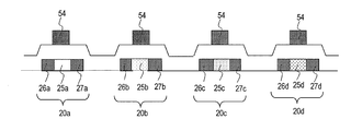
- 2 is a cross-sectional view schematically showing a configuration in the vicinity of semiconductor layers 20a to 20d of the semiconductor device 100.
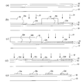
- FIG. FIGS. 4A to 4E are cross-sectional views schematically showing a method for manufacturing the semiconductor device 100.
- FIG. (A) And (b) is sectional drawing which represented the manufacturing method of the semiconductor device 100 typically.
- (A) to (c) are tables for explaining three types of processing methods for the semiconductor layers 20a to 20d.
- (A) And (b) is a graph for demonstrating the effect by the semiconductor device 100.
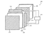
- FIG. It is the perspective view which represented typically the structure of the display apparatus 200 by embodiment of this invention.
- FIG. 4 is a plan view schematically showing a configuration of a TFT substrate 210 in a display region 260 of the display device 200.
- FIG. 4 is a plan view schematically showing the entire configuration of a TFT substrate 210 in the display device 200.
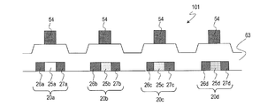
- FIG. FIG. 6 is a cross-sectional view schematically showing a configuration in the vicinity of semiconductor layers 20a to 20d of a semiconductor device 101 according to a second embodiment of the present invention.
- FIGS. 4A to 4E are cross-sectional views schematically showing a method for manufacturing the semiconductor device 101.
- FIG. (A) to (e) are tables for explaining five types of processing methods for the semiconductor layers 20a to 20d in the semiconductor device 101.
- FIG. 6 is a cross-sectional view schematically showing a configuration in the vicinity of semiconductor layers 20a to 20d of a semiconductor device 102 according to a third embodiment of the present invention.
- FIGS. 4A to 4E are cross-sectional views schematically showing a method for manufacturing the semiconductor device 102.
- FIG. (A) and (b) are tables for explaining two types of processing methods for the semiconductor layers 20a to 20d in the semiconductor device 102.
- FIG. 1 is a cross-sectional view schematically showing the configuration of the semiconductor device 100 according to the first embodiment of the present invention
- FIG. 2 schematically shows the configuration in the vicinity of the semiconductor layers 20a to 20d of the semiconductor device 100.
- the semiconductor device 100 includes staggered TFTs 10a, 10b, 10c, and 10d having a top gate structure.
- the TFTs 10a and 10b are P-type TFTs (p-channel TFTs), and the TFTs 10c and 10d are N-type TFTs (n-channel TFTs).
- the TFT 10a and the TFT 10d are used as a high voltage operation TFT in which a relatively high voltage is applied between the source and the drain, and the TFT 10b and the TFT 10c are lower than the high voltage operation TFT between the source and the drain. It is used as a TFT for low voltage operation to which a voltage is applied.
- TFTs 10a, 10b, 10c, and 10d (hereinafter may be abbreviated as 10a to 10d, and other reference numbers may be abbreviated in the same manner), respectively, a first P-type TFT, a second P-type TFT, Sometimes referred to as a first N-type TFT and a second N-type TFT.
- FIG. 2 illustrate only four TFTs included in the semiconductor device 100, the semiconductor device 100 includes at least four types of TFTs 10a to 10d, and other types of the same or other types.
- a TFT may be provided.
- the semiconductor device 100 includes a substrate (transparent substrate, insulating substrate, etc.) 61 made of glass, insulating resin, and the like, and an undercoat layer 62 formed on the substrate 61.
- the TFTs 10a to 10d are respectively
- the semiconductor layers 20a, 20b, 20c, and 20d made of polycrystalline silicon (polysilicon) are formed on the undercoat layer 62.
- the semiconductor layers 20a to 20d may be made of non-single crystal non-amorphous silicon such as microcrystalline silicon. There may be a configuration of the semiconductor device 100 that does not include the undercoat layer 62.
- a gate insulating layer (gate insulating film) 63 and an insulating layer (interlayer insulating film) 64 are stacked on the semiconductor layers 20a to 20d.
- the gate insulating layer 63 corresponds to each of the TFTs 10a to 10d.
- a plurality of gates 54 are formed on a gate electrode 55, a source electrode 56, and a drain electrode 57 on an insulating layer 64.
- the semiconductor layers 20a to 20d include source contact regions (first contact regions) 26a, 26b, 26c and 26d, drain contact regions (second contact regions) 27a, 27b, 27c and 27d, and both contact regions, respectively. Channel regions 25a, 25b, 25c and 25d located between the two.
- the source contact regions 26a to 26d are connected to the corresponding source electrodes 56 through the contact holes of the gate insulating layer 63 and the insulating layer 64, respectively.
- the drain contact regions 27a to 27d are connected to the gate insulating layer 63 and the insulating layer, respectively.
- Each is connected to a corresponding drain electrode 57 through 64 contact holes.
- Each gate 54 is connected to a corresponding gate electrode 55 through a contact hole in the insulating layer 64.
- the channel regions 25b, 25c, and 25d are doped with a p-type impurity such as B (boron).
- the channel region 25a is not doped with impurities.
- the concentrations of the impurities doped in the channel regions 25a to 25d are different from each other, and the p-type impurity concentrations (including the case where the concentration is 0) in the channel regions 25a to 25d are d1, d2, d3, and d4, respectively.
- d1, d2, d3, and d4 satisfy the relationship of d1 ⁇ d2 ⁇ d3 ⁇ d4.
- a layer of silicon oxide film (SiOx), silicon nitride film (SiNx) or the like is laminated on the substrate 61 to about 300 nm by PCVD (plasma CVD) method, LPCDV (low pressure CVD) method, sputtering method, or the like.
- a coat layer 62 is obtained.
- the undercoat layer 62 is provided to prevent impurities from diffusing from the substrate 61 into the semiconductor layers 20a to 20d. However, if the diffusion of impurities does not cause a problem, the undercoat layer 62 should not be formed. There is also a possibility.
- an amorphous silicon layer (a-Si layer) 22 is formed on the undercoat layer 62 by laminating amorphous silicon (a-Si) to a thickness of about 20 to 100 nm by PCVD, LPCDV, sputtering, or the like. As a result, the laminated structure shown in FIG. When the a-Si layer 22 is stacked using the PCVD method, dehydrogenation is performed after the stacking.
- a resist 30 is stacked on the a-Si layer 22, and openings of the resist 30 are provided on the regions 22b and 22d of the a-Si layer 22 by photolithography.
- the regions 22a (first region), 22b (second region), 22c (third region), and 22d (fourth region) of the a-Si layer 22 are the semiconductors shown in FIGS. This is the region where the layers 20a, 20b, 20d and 20d are formed.
- the p-type impurity (B in this embodiment) as the dopant 31 is selectively doped into the regions 22b and 22d by an ion implantation method or the like (first doping step (first step)).
- the resist 30 is laminated again on the a-Si layer 22, and the regions 22c and 22d of the a-Si layer 22 are formed by photolithography. An opening of the resist 30 is provided on the top.
- B as the dopant 31 is selectively doped into the regions 22c and 22d by an ion implantation method or the like (second doping step (second step)).
- a laser beam 32 such as an excimer laser
- the semiconductor layer 22 is made of a polysilicon layer.
- the laser beam 32 a pulse laser, a CW (continuous wave) laser, or the like can be used.
- the polysilicon layer 23 is partially removed by photolithography to obtain polysilicon regions 23a to 23d.
- a silicon oxide film is laminated to a thickness of about 30 to 200 nm by the PCVD method, the LPCDV method, the sputtering method or the like so as to cover the polysilicon regions 23a to 23d, thereby forming the gate insulating layer 63.
- aluminum (Al) is deposited on the gate insulating layer 63 to a thickness of about 100 to 500 nm by sputtering.
- aluminum is patterned by using a photolithography method and a wet etching method, and the photoresist is peeled off and the substrate is washed to form a plurality of gates 54 as shown in FIG.
- the metal constituting the gate 54 is not limited to aluminum.
- a simple metal such as molybdenum (Mo), or a material containing nitrogen, oxygen, or another metal in these metals may be used.
- a PCVD method or the like can be used instead of the sputtering method.
- a dry etching method may be used instead of the wet etching method.
- the upper portions of the polysilicon regions 23a and 23b are selectively covered with a resist, and the upper portions of the polysilicon regions 23c and 23d are respectively covered.
- P phosphorus
- the polysilicon regions 23c and 23d excluding the lower portion of the gate 54 are doped with P, so that the source contact regions 26c and 26d and the drain contact regions 27c and 27d of the TFTs 10c and 10d, which are N-type TFTs, are formed.
- the polysilicon regions 23c and 23d covered by the gate 54 are not doped with P, and these portions become the channel regions 25c and 25d of the TFTs 10c and 10d.
- the semiconductor layers 20c and 20d of the TFTs 10c and 10d are completed.
- the upper portions of the semiconductor layers 20c and 20d are selectively covered with a resist, and the upper portions of the polysilicon regions 23a and 23b are respectively covered.
- the dopant 54 is doped with B as a mask.
- the polysilicon regions 23a and 23b except for the lower portion of the gate 54 are doped with B to form the source contact regions 26a and 26b and the drain contact regions 27a and 27b of the TFTs 10a and 10b which are P-type TFTs.
- the polysilicon regions 23a and 23b covered by the gate 54 are not doped with B, and these portions become the channel regions 25a and 25b of the TFTs 10a and 10b.
- the semiconductor layers 20a and 20b of the TFTs 10a and 10b are completed.
- the gate insulating layer 63 on the source contact layers 26a to 26d and the drain contact layers 27a to 27d and Contact holes are formed in the insulating layer 64 and the insulating layer 64 on each gate 54.
- a metal material such as aluminum is laminated on the insulating layer 64 so as to fill the contact hole, and shaping by photolithography is performed, whereby an electrode gate electrode 55, a source electrode 56, and a drain electrode 57 are formed for each TFT.
- (A) of FIG. 5 represents the relationship of the amount (D) of B doped into the regions 22a to 22d in the two doping steps (first doping example).
- the regions 22b and 22d are doped with an amount of B
- the regions 22c and 22d are doped with an amount of B that is larger than the amount a.
- the final dose amounts for the regions 22a to 22d are 0, a, b (> a), and a + b, respectively.
- This dose amount is reflected in the impurity concentration of B in the channel regions 25a to 25d of the TFTs 10a to 10d shown in FIGS.
- the impurity concentrations d1, d2, d3, and d4 of the channel regions 25a to 25d satisfy the relationship of d1 ⁇ d2 ⁇ d3 ⁇ d4.
- FIG. 5 represents the relationship of the dose (D) of the regions 22a to 22d according to the second doping example of the present embodiment. As shown in this figure, the doping process is performed twice also in the second doping example.
- the regions 22c and 22d are doped with an amount B
- the regions 22b and 22d are doped with an amount b (> a).
- the final dose amounts for the regions 22a to 22d are 0, b (> a), a, and a + b, respectively.
- the impurity concentrations d1, d2, d3, and d4 of the channel regions 25a to 25d satisfy the relationship d1 ⁇ d3 ⁇ d2 ⁇ d4.
- the third doping step includes the second doping step shown in FIG. 3C, the further formation of the resist 30, and the opening of the resist 30, and then the annealing step shown in FIG. Implemented before.
- the regions 22a to 22d are doped with an amount c of B, and in the second doping, the regions 22b and 22d are doped with an amount B (> c) of the third doping. As a result, the regions 22c and 22d are doped with an amount b (> a) of B. As a result, the final dose amounts for the regions 22a to 22d are c, a + c, b + c (> a + c), and a + b + c, respectively. As a result, the impurity concentrations d1, d2, d3, and d4 of the channel regions 25a to 25d satisfy the relationship of d1 ⁇ d2 ⁇ d3 ⁇ d4.
- the first to third doping examples are merely examples, and the doping example of the first embodiment is not limited to the above examples.
- the value of a may be different from each other, and the value of b may be different from each other.
- d1, d2, d3, and d4 satisfy the relationship of d1 ⁇ d2 and d3 ⁇ d4.
- the introduction of impurities into the polysilicon regions 23a to 23d is performed before the formation of the gate insulating layer 63. It can also be done after forming.
- the dose amounts to the channel regions 25a to 25d are, for example, 5e11 to 2e12 (atoms / cm 2 ), 1e12 to 2.5e12 (atoms / cm 2 ), with acceleration energy (injection energy) of 25 keV. 5e12 to 3e12 (atoms / cm 2 ), and 2e12 to 4e12 (atoms / cm 2 ).
- conventional semiconductor devices employ a dose of 1e12 (atoms / cm 2 ), CD dope of 2e12 (atoms / cm 2 ), and a total of 3e12 (atoms / cm 2 ) over the entire substrate surface. ing.
- n-type impurities such as P (phosphorus) as well as p-type impurities such as B may be used as the dopant.
- P may be used as the dopant for the second doping in the first doping example.
- d1, d2, d3, and d4 are values obtained by subtracting the concentration of the n-type impurity (including the case of concentration 0) from the concentration of the p-type impurity (including the case of concentration 0) in the channel regions 25a to 25d. .
- the channel region 25a of the TFT 10a is not doped with impurities, the channel region 25a may be doped with the same amount of p-type impurity and n-type impurity so that d1 is zero. In any case, in the present embodiment, the relationship of d1 ⁇ d2 and d3 ⁇ d4 is satisfied.
- FIG. 6 is a graph for explaining the effect of the semiconductor device 100.
- FIG. 6A shows the voltage dependence (Id-Vg characteristic) of each mobility of the high voltage TFT and the low voltage TFT having the same impurity concentration in the channel region. Represents the characteristics of the high voltage TFT, and b1 represents the characteristics of the low voltage TFT.
- FIG. 6B shows the Id-Vg characteristics of the high voltage TFT having a high channel region impurity concentration and the low voltage TFT having a channel region impurity concentration lower than that of the high voltage TFT. Represents the characteristics of the high voltage TFT, and b2 represents the characteristics of the low voltage TFT.
- the threshold voltage of the low-voltage TFT becomes higher than the threshold voltage of the high-voltage TFT.
- the impurity concentration of the high voltage TFT is higher than the impurity concentration of the low voltage TFT, such as the high voltage TFT 10d and the low voltage TFT 10c of the present embodiment, the threshold voltage of the high voltage TFT is higher. It becomes possible to keep the threshold voltage of the low voltage TFT low. Therefore, when the TFT 10c is used, for example, as a TFT for switching a peripheral circuit in a display device, it is possible to reduce the leakage current and suppress the power consumption of the device.
- the example shown in FIG. 6 is one of the advantages of the semiconductor device according to the present embodiment. By appropriately changing the impurity concentration in the channel region of the TFTs 10a to 10d in accordance with each circuit, high performance and low performance are achieved. A semiconductor device with power consumption can be provided with high manufacturing efficiency.
- the threshold voltage of each TFT is set to, for example, a low voltage TFT
- the threshold voltage of the semiconductor device or the equipment including the semiconductor device can be set unnecessarily. It is possible to execute without increasing the power consumption.
- the display device 200 will be described as a liquid crystal display device.
- the display device 200 of the present invention is not limited to the liquid crystal display device, and an organic electroluminescence (EL) display device including an active matrix substrate having a plurality of TFTs, Other types of display devices such as inorganic electroluminescence display devices may be used.
- EL organic electroluminescence
- FIG. 7 is a perspective view schematically showing the configuration of the display device 200
- FIG. 8 is a plan view schematically showing the configuration of the TFT substrate 210 in the display region 260 of the display device 200
- FIG. 2 is a plan view schematically showing the overall configuration of a substrate 210.
- the display device 200 includes a TFT substrate 210 and a counter substrate (CF substrate) 220 that face each other with the liquid crystal layer 230 interposed therebetween, and polarizing plates disposed on the outer sides of the TFT substrate 210 and the counter substrate 220. 215 and 216, and a backlight unit 240 that emits display light toward the polarizing plate 215.
- CF substrate counter substrate
- the display area 260 of the display device 200 includes a plurality of pixels 250 arranged in a matrix.
- a plurality of scanning lines (gate bus lines) 254 and a plurality of signal lines (data bus lines) 256 extend on the TFT substrate 210 so as to be orthogonal to each other.
- the TFT 10 according to the present invention is arranged for each pixel 250 as an active element.
- one pixel is defined as a region delimited by two adjacent scanning lines 254 and two adjacent signal lines 256.
- An auxiliary capacitance line (also referred to as a storage capacitance line or Cs line) 258 may extend between two adjacent scanning lines 254 in parallel with the scanning line 254.
- the plurality of scanning lines 254 and the plurality of signal lines 256 are respectively connected to the gate driver (scanning line driving circuit) 212 and the data driver (signal line driving circuit) 213 shown in FIG.
- Signals from the gate driver 212 and the data driver 213 are controlled by the display controller 214, and in response to the control, a scanning signal for switching on / off of the TFT 10 is supplied from the gate driver 212 to the plurality of scanning lines 254. Further, in accordance with control by the display controller 214, a display signal (voltage applied to the pixel electrode 252) is supplied from the data driver 213 to the plurality of signal lines 256.
- the counter substrate 220 shown in FIG. 7 includes a color filter and a common electrode.
- each of the color filters is an R (red) filter and a G (green) arranged corresponding to each pixel. Filter, and B (blue) filter.
- the common electrode is formed so as to cover the plurality of pixel electrodes 252. In accordance with the potential difference applied between the common electrode and each pixel electrode 252, the liquid crystal molecules between both electrodes are aligned for each pixel 250, and display is performed.
- a power supply circuit 261, a memory 262, a common driver 264, and the like are formed in addition to the display area 260, the gate driver 212, the data driver 213, and the display controller 214.
- the TFTs 10a to 10d of this embodiment are used as TFTs for the display area 260, the gate driver 212, the data driver 213, the display controller 214, the power supply circuit 261, the memory 262, the common driver 264, and the like.
- the threshold voltage can be kept low, so that the operation of the peripheral circuit is speeded up and leakage current is increased. Alternatively, power consumption can be reduced. Therefore, it is possible to provide a high-quality and low-power consumption display device having high resolution with high manufacturing efficiency.
- the semiconductor device 101 includes four types of TFTs 10a to 10d as in the first embodiment, and the overall configuration is almost the same as that shown in FIG. Hereinafter, the description will be focused on the parts different from the first embodiment, but the configuration, functions, effects, and the like are the same as those of the first embodiment, except as specifically described.
- the semiconductor device 101 and the four types of TFTs 10a to 10d of the present embodiment can also be applied to the display device 200 described in the first embodiment.
- FIG. 10 is a cross-sectional view schematically showing the configuration of the semiconductor device 101 near the semiconductor layers 20a to 20d.
- the semiconductor layers 20a to 20d of the four types of TFTs 10a to 10d in the semiconductor device 101 are respectively composed of source contact regions 26a to 26d, drain contact regions 27a to 27d, and channel regions 25a to 25d.
- the channel regions 25b, 25c, and 25d are doped with p-type impurities such as B, and the channel region 25a is not doped with impurities.
- the undercoat layer 62 is formed on the substrate 61, and then the amorphous silicon layer 22 is stacked on the undercoat layer 62.
- a resist 30 is stacked on the a-Si layer 22, and openings of the resist 30 are formed on the regions 22b to 22d (second to fourth regions) by photolithography. And doping the regions 22b to 22d with B (first doping step (first step)).
- the resist 30 is again laminated on the a-Si layer 22, an opening is provided on the region 22d, and B is doped into the region 22d. (Second doping step (second step)).
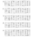
- FIG. 12 is a table for explaining five types of dope treatment methods in forming the semiconductor layers 20a to 20d of the semiconductor device 101.
- FIG. 12A shows the relationship of the amount (D) of B doped in the regions 22a to 22d in the two doping steps (first doping example) in the manufacturing method of the semiconductor device 101.
- the region 22b to 22d is doped with an amount of B
- the region 22d is doped with an amount of B greater than the amount a.
- the final dose amounts for the regions 22a to 22d are 0, a, a, and a + b, respectively.
- FIG. 12B shows the relationship of the dose (D) according to the second doping example of this embodiment.
- the region 22d in the first doping, the region 22d is doped with an amount B, and in the second doping, the regions 22b to 22d are doped with an amount b (> a).
- (C) in FIG. 12 represents the relationship of the dose (D) according to the third doping example of the present embodiment.
- the regions 22a, 22c, and 22d are doped with an amount B, and the second doping causes the regions 22b and 22d to have an amount b (> a) B.
- the doses of the regions 22a to 22d are a, b, a, and a + b, respectively, and the impurity concentrations d1, d2, d3, and d4 satisfy the relationship of d1 ⁇ d2 and d3 ⁇ d4.
- (D) of FIG. 12 represents the relationship of the dose (D) by the 4th doping example of this embodiment.
- the regions 22a and 22d are doped with an amount B
- the regions 22b to 22d are doped with an amount b (> a).
- (E) of FIG. 12 represents the relationship of the dose (D) by the 5th doping example of this embodiment. As shown in this figure, in the fifth doping example, doping is performed three times (third step).
- the region 22a to 22d is all doped with the amount c of B
- the region 22b to 22d is doped with the amount a B
- the region 22d is doped.
- the quantity b (> a) of B is doped.
- the dose amounts of the regions 22a to 22d are c, a + c, a + c, and a + b + c, respectively.
- the third doping step is performed after the second doping step shown in FIG. 11C, the formation of the resist 30 and the opening of the resist 30 and before the annealing step. .
- the third step may be performed before the first step or between the first step and the second step. Further, a process similar to the third process may be added to the first to fourth doping examples.
- first to fifth doping examples are merely examples, and the doping example of the second embodiment is not limited to the above examples.
- the value of a may be different from each other, and the value of b may be different from each other.
- d1, d2, d3, and d4 satisfy the relationship of d1 ⁇ d2 and d3 ⁇ d4.
- d1, d2, d3, and d4 are the concentrations of the p-type impurities in the channel regions 25a to 25d (when the concentration is 0).
- the impurity concentration in at least three of the channel regions of at least four types of TFTs formed on the same substrate can be made different, for example, the threshold value of the low voltage TFT
- the characteristics of the TFT can be appropriately set for each circuit in which the TFT is used, for example, by suppressing the voltage below the threshold voltage of the high-voltage TFT, a wide variety of controls in a semiconductor device or a device including the semiconductor device are not allowed. It becomes possible to execute without increasing the power consumption.
- only two photolithography processes and two or three doping processes are required, so that it is possible to improve the manufacturing efficiency of a semiconductor device including various TFTs.
- the semiconductor device 102 also includes four types of TFTs 10a to 10d. Since the overall configuration is substantially the same as that shown in FIG. 1, illustration thereof is omitted here. Hereinafter, the description will be focused on the parts different from the first embodiment, but the configuration, functions, effects, and the like are the same as those of the first embodiment, except as specifically described.
- the semiconductor device 102 and the four types of TFTs 10a to 10d of this embodiment can also be applied to the display device 200 described in the first embodiment.
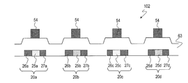
- FIG. 13 is a cross-sectional view schematically showing a configuration in the vicinity of the semiconductor layers 20a to 20d of the semiconductor device 102.
- the semiconductor layers 20a to 20d of the four types of TFTs 10a to 10d in the semiconductor device 101 are composed of source contact regions 26a to 26d, drain contact regions 27a to 27d, and channel regions 25a to 25d, respectively.
- the channel regions 25a to 25d are doped with a p-type impurity such as B.
- the channel regions 25a and 25c have the same dose, and the channel regions 25b and 25d have the same dose.
- d1, d2, d3, and d4 have a relationship of d1 ⁇ d2 and d3 ⁇ d4.
- the undercoat layer 62 is formed on the substrate 61, and then the amorphous silicon layer 22 is stacked on the undercoat layer 62.
- a resist 30 is stacked on the a-Si layer 22, and the resist 30 is formed on the regions 22a (first region) and 22c (third region) by photolithography. And the regions 22a and 22c are doped with B (first doping step (first step)).
- the resist 30 is again laminated on the a-Si layer 22 to form the regions 22b (second region) and 22d (fourth region). An opening is provided above, and the regions 22b and 22d are doped with B (second doping step (second step)).
- FIG. 15 is a table for explaining two types of dope treatment methods in forming the semiconductor layers 20a to 20d of the semiconductor device 102.
- FIG. 15A shows the relationship of the amount (D) of B doped in the regions 22a to 22d in the two doping steps (first doping example) in the manufacturing method of the semiconductor device 102.
- the regions 22a and 22c are doped with an amount of B
- the regions 22b and 22d are doped with an amount of B greater than the amount a.
- the final dose amounts for the regions 22a to 22d are a, b, a, and b, respectively.
- the impurity concentrations d1, d2, d3, and d4 of the channel regions 25a to 25d satisfy the relationship of d1 ⁇ d2 and d3 ⁇ d4.
- FIG. 15B shows the relationship of the dose (D) according to the second doping example of this embodiment.
- the region 22a to 22d is doped with the amount c of B
- the region 22b and 22d is doped with the amount a of B.
- the final dose amounts for the regions 22a to 22d are c, c + a, c, and c + a, respectively, and the impurity concentrations d1, d2, d3, and d4 satisfy the relationship of d1 ⁇ d2 and d3 ⁇ d4. .
- d1, d2, d3, and d4 are the concentrations of the p-type impurities in the channel regions 25a to 25d (when the concentration is 0).
- the channel region 25a to 25d (and the region 22a to 22d in the manufacturing process) is doped with the p-type impurity concentration (including the case where the concentration is 0) to the n-type impurity (including the case where the concentration is 0).
- a method for manufacturing the display device 200 according to the present invention includes the method for manufacturing the semiconductor device described above.
- the threshold voltage of the low-voltage TFT formed on the same substrate can be appropriately set for each circuit in which it is used, such as suppressing the threshold voltage of the high-voltage TFT below the threshold voltage.
- Various kinds of control in the semiconductor device or the device including the semiconductor device can be executed without unnecessarily increasing the power consumption.
- the present invention is suitably used for a display device such as a liquid crystal display device including an active matrix substrate having a thin film transistor, an organic electroluminescence (EL) display device, an inorganic electroluminescence display device, or various types of semiconductor devices.
- a display device such as a liquid crystal display device including an active matrix substrate having a thin film transistor, an organic electroluminescence (EL) display device, an inorganic electroluminescence display device, or various types of semiconductor devices.
Landscapes
- Thin Film Transistor (AREA)
- Chemical & Material Sciences (AREA)
- Crystallography & Structural Chemistry (AREA)
Abstract
本発明は、多種の用途に対応可能な複数のTFTが形成された半導体装置を製造効率よく提供することを目的とし、本発明による半導体装置(100)は、それぞれが多結晶シリコンからなるチャネル領域を有する第1P型TFT(10a)、第2P型TFT(10b)、第1N型TFT(10c)、及び第2N型TFT(10d)を備え、TFT(10a~10d)のチャネル領域におけるp型不純物の濃度をそれぞれd1、d2、d3、及びd4とした場合、d1、d2、d3、及びd4のうちの少なくとも3つの値が互いに異なり、d1、d2、d3、及びd4が、d1<d2、且つd3<d4の関係を満たす。
Description
本発明は、複数の薄膜トランジスタ(TFT)を備えた半導体装置に関する。また、本発明は、液晶表示装置、有機EL表示装置等の表示装置に用いる半導体装置、及びそのような半導体装置を備えた表示装置に関する。
近年、携帯端末機器、ノートパソコン、TV等の表示機器として、液晶表示装置や有機EL表示装置等が用いられている。これらの表示装置は、半導体装置としてのアクティブマトリクス基板を備えている。アクティブマトリクス基板には、マトリクス状に配置された複数の画素のそれぞれにおいて画素電極への電圧印加をスイッチングするTFTが形成されている。さらに、アクティブマトリクス基板には複数の画素への表示電圧、ゲート電圧等の制御を行なう駆動回路のTFTが、表示領域の周辺に配置されている。これらのTFTには、非結晶(アモルファス)シリコンTFT、微結晶シリコンTFT、多結晶シリコン(ポリシリコン)TFTなどが用いられている。
複数のTFTを備えた半導体装置の例が特許文献1に記載されている。この文献に記載された半導体装置は、2種類のnチャネル型TFT及び2種類のpチャネル型TFTを備えている。これらのnチャネル型TFT及びpチャネル型TFTはいずれも多結晶シリコンからなる活性層を有している。2種類のnチャネル型TFTは、互いに閾値電圧(Vt)の異なる2種類のTFTを含み、2種類のpチャネル型TFTも、互いに閾値電圧の異なる2種類のTFTを含んでいる。また、2種類のnチャネル型TFTの一方のチャネル領域と2種類のpチャネル型TFTの一方のチャネル領域には、ドーパントが同じ濃度でドープされており、2種類のnチャネル型TFTの他方のチャネル領域と2種類のpチャネル型TFTの他方のチャネル領域はドーパントがドープされないノンドープ領域であるとされている。
液晶表示装置などの表示装置の基板には、マトリクス状に配列された画素からなる表示部や、表示部の外に形成されたゲートドライバやデータドライバ等の駆動回路が形成されるが、近年の薄膜形成技術の向上に伴い、表示部におけるTFTと駆動回路等に用いられるTFTとを、同じ基板上に多結晶シリコンを用いて一括して形成することが可能となっている。
このような表示装置のTFT基板、または高機能を要求される装置におけるTFT基板上には、例えば、ローレベルとハイレベルの2値レベルを用いたデジタル処理を行うロジック回路や、画素電極等の印加電圧の制御などアナログ電圧の処理を行う回路が形成され、これらの回路に応じた特性の異なる複数種のTFTがTFT基板上に同時に形成される。
ロジック回路やスイッチに用いられるTFTでは、オン状態においてスイッチングに必要とされる電流駆動能力があればよく、オフ状態では電流を極力流さないようにしてリーク電流を抑えることが求められる。一方、アナログ電圧を制御するTFTは、オン状態とされる時間が長く、オン状態におけるソース・ドレイン電圧を広い電圧幅にわたって精度よく制御できることが重要である。
例えば、液晶表示装置の表示領域において液晶を駆動するためには、画素電極にはほぼ0Vから10Vを超えるような高い印加電圧加えることが要求されるが、このような広い幅のソース・ドレイン電圧を高精度で制御するためには、TFTの閾値電圧は低く抑えられることが望ましい。また、これと同時に、比較的低い電圧による精密かつ高速動作が要求される周辺回路においては、その消費電力を不必要に増加させないことが要求される。特に、近年、携帯機器の長時間駆動や環境問題等への対応のため、各機器に対する消費電力低減化の要求はますます高まっており、1つの機器の中に複数のTFTを多種用途に用いつつ、それらリーク電流を極力抑えることが重要となっている。
しかし、チャネル領域における不純物濃度が同じであるTFTを駆動電圧の異なる回路に用いた場合、高電圧動作が必要なTFTよりも低電圧動作用のTFTのほうが、閾値電圧が高くなり、リーク電流が大きくなるという問題が生じ得る。上記の特許文献1の半導体装置では、複数のTFTにおけるチャネル領域の不純物濃度が2種類であるため、このような問題に十分に対処することができないという問題がある。また、2種類のp型TFTの一方と2種類のn型TFTの一方の不純物濃度が同じであるため、p型TFTとn型TFT両方の閾値電圧をほぼ同じ値に下げることも容易ではない。
この問題を解決するためには、低電圧動作用のTFTにおいてはチャネル長を短くするなどの対応が考えられるが、それでも閾値電圧を必要な値まで低減させるには十分ではなかった。また、上記問題を解決するために、TFT形成工程においてTFT毎に異なるドープ処理を行って、チャネル領域の不純物濃度をTFT毎に変えることが考えられるが、これでは製造工程が複雑化し、製造コスト及び製造時間が増大するという問題が発生する。
本発明は、このような問題を解決するためになされたものであり、多種の用途に適切に応じることが可能な複数種のTFTを備えた半導体装置または表示装置を、製造効率よく提供することを目的の一つとする。また、本発明は、消費電力が低減された多機能な半導体装置または表示装置を、製造効率よく提供することを目的の一つとする。
本発明による半導体装置は、それぞれが多結晶シリコンからなるチャネル領域を有する第1P型TFT、第2P型TFT、第1N型TFT、及び第2N型TFTを備え、前記第1P型TFT、前記第2P型TFT、前記第1N型TFT、及び前記第2N型TFTのチャネル領域におけるp型不純物の濃度をそれぞれd1、d2、d3、及びd4とした場合、前記d1、d2、d3、及びd4のうちの少なくとも3つの値が互いに異なり、前記d1、d2、d3、及びd4が、d1<d2、且つd3<d4の関係を満たす。
ある実施形態では、前記第1P型TFT及び前記第2N型TFTが高電圧駆動用のTFTであり、前記第2P型TFT及び前記第1N型TFTが、前記高電圧駆動用のTFTよりも低いソース-ドレイン電圧を制御するための低電圧駆動用TFTである。
ある実施形態では、前記d1、d2、d3、及びd4の4つの値が互いに異なっている。
ある実施形態では、前記d1、d2、d3、及びd4が、d1<d2<d3<d4の関係、又はd1<d3<d2<d4の関係を満たす。
ある実施形態では、前記d1、d2、d3、及びd4のうちの3つの値が互いに異なっており、前記d1、d2、d3、及びd4のうちの2つの値が互いに等しい。
ある実施形態では、前記d1、d2、d3、及びd4が、d1<d2=d3<d4の関係、又はd1=d3<d2<d4の関係を満たす。
ある実施形態では、前記d1、d2、d3、及びd4が、それぞれ、前記第1P型TFT、前記第2P型TFT、前記第1N型TFT、及び前記第2N型TFTのチャネル領域におけるp型不純物の濃度(濃度0の場合を含む)からn型不純物(濃度0の場合を含む)の濃度を引いた値を意味する。
本発明による表示装置は、上記の半導体装置を含む表示装置である。
本発明による他の半導体装置は、それぞれが多結晶シリコンからなるチャネル領域を有する第1P型TFT、第2P型TFT、第1N型TFT、及び第2N型TFTを備え、前記第1P型TFT及び前記第2N型TFTが高電圧駆動用のTFTであり、前記第2P型TFT及び前記第1N型TFTが、前記高電圧駆動用のTFTよりも低いソース-ドレイン電圧を制御するための低電圧駆動用TFTであり、前記第1P型TFT、前記第2P型TFT、前記第1N型TFT、及び前記第2N型TFTのチャネル領域におけるp型不純物の濃度をそれぞれd1、d2、d3、及びd4とした場合、前記d1、d2、d3、及びd4が、d1=d3<d2、d1=d3<d4、d1<d2=d4、又はd3<d2=d4の関係を満たす。
ある実施形態では、前記d1、d2、d3、及びd4が、d1=d3<d2=d4の関係を満たす。
ある実施形態では、前記d1、d2、d3、及びd4が、それぞれ、前記第1P型TFT、前記第2P型TFT、前記第1N型TFT、及び前記第2N型TFTのチャネル領域におけるp型不純物の濃度(濃度0の場合を含む)からn型不純物(濃度0の場合を含む)の濃度を引いた値を意味する。
本発明による他の表示装置は、上記半導体装置を含む表示装置である。
本発明による半導体装置の製造方法は、それぞれが多結晶シリコンからなるチャネル領域を有する第1P型TFT、第2P型TFT、第1N型TFT、及び第2N型TFTを備えた半導体装置の製造方法であって、前記第1P型TFT、前記第2P型TFT、前記第1N型TFT、及び前記第2N型TFTのそれぞれのチャネル領域となる第1領域、第2領域、第3領域、及び第4領域のうちの少なくとも1つの領域に対して、第1の量の不純物を同時にドープする第1工程と、前記第1工程の前または後に、前記第1領域、前記第2領域、前記第3領域、及び前記第4領域のうち、前記第1工程において不純物がドープされる領域の少なくとも1つを含む複数の領域に対して、前記第1の量とは異なる第2の量の不純物を同時にドープする第2工程と、を含み、前記第1領域、前記第2領域、前記第3領域、及び前記第4領域にドープされるp型不純物の濃度をそれぞれd1、d2、d3、及びd4とした場合、前記d1、d2、d3、及びd4が、d1<d2、且つd3<d4の関係を満たす。
ある実施形態では、前記第1P型TFT及び前記第2N型TFTが高電圧駆動用のTFTであり、前記第2P型TFT及び前記第1N型TFTが、前記高電圧駆動用のTFTよりも低いソース-ドレイン電圧を制御するための低電圧駆動用TFTである。
ある実施形態では、前記第1工程において、前記第1領域、前記第2領域、前記第3領域、及び前記第4領域の2つの領域に対して、前記第1の量の不純物が同時にドープされ、前記第1工程の後に前記第2工程が実施され、前記第2工程では、前記第1領域、前記第2領域、前記第3領域、及び前記第4領域のうち、前記第1工程において不純物がドープされた領域の1つと、前記第1工程において不純物がドープされなかった領域の1つの領域に対して、前記第1の量とは異なる第2の量の不純物が同時にドープされる。
ある実施形態では、前記d1、d2、d3、及びd4の4つの値が互いに異なっている。
ある実施形態では、前記d1、d2、d3、及びd4が、d1<d2<d3<d4の関係、又はd1<d3<d2<d4の関係を満たす。
ある実施形態では、前記第1工程において、前記第2領域及び前記第4領域に対して、前記第1の量の不純物が同時にドープされ、前記第2工程では、前記第3領域及び前記第4領域に対して、前記第1の量よりも多い前記第2の量の不純物が同時にドープされる。
ある実施形態では、前記第1工程において、前記第3領域及び前記第4領域に対して、前記第1の量の不純物が同時にドープされ、前記第2工程では、前記第2領域及び前記第4領域に対して、前記第1の量よりも多い前記第2の量の不純物が同時にドープされる。
ある実施形態は、前記第1領域、前記第2領域、前記第3領域、及び前記第4領域に対して、第3の量の不純物をドープする第3の工程を含む。
ある実施形態では、前記d1、d2、d3、及びd4のうちの3つの値が互いに異なっており、前記d1、d2、d3、及びd4のうちの2つの値が互いに等しい。
ある実施形態では、前記d1、d2、d3、及びd4が、d1<d2=d3<d4の関係、又はd1=d3<d2<d4の関係を満たす。
ある実施形態では、前記第1工程において、前記第2領域、前記第3領域、及び前記第4領域に対して、前記第1の量の不純物が同時にドープされ、前記第2工程では、前記第4領域に対して、前記第1の量よりも多い前記第2の量の不純物がドープされる。
ある実施形態では、前記第1工程において、前記第4領域に対して、前記第1の量の不純物がドープされ、前記第2工程では、前記第2領域、前記第3領域、及び前記第4領域に対して、前記第1の量よりも多い前記第2の量の不純物が同時にドープされる。
ある実施形態では、前記第1工程において、前記第1領域、前記第3領域、及び前記第4領域に対して、前記第1の量の不純物が同時にドープされ、前記第2工程では、前記第2領域及び前記第4領域に対して、前記第1の量よりも多い前記第2の量の不純物が同時にドープされる。
ある実施形態では、前記第1工程において、前記第1領域及び前記第4領域に対して、前記第1の量の不純物が同時にドープされ、前記第2工程では、前記第2領域、前記第3領域、及び前記第4領域に対して、前記第1の量よりも多い前記第2の量の不純物が同時にドープされる。
ある実施形態は、さらに、前記第1領域、前記第2領域、前記第3領域、及び前記第4領域に対して、第3の量の不純物が同時にドープされる工程を含む。
ある実施形態では、前記d1、d2、d3、及びd4が、それぞれ、前記第1P型TFT、前記第2P型TFT、前記第1N型TFT、及び前記第2N型TFTのチャネル領域におけるp型不純物の濃度(濃度0の場合を含む)からn型不純物(濃度0の場合を含む)の濃度を引いた値を意味する。
本発明による表示装置の製造方法は、上記製造方法を含む表示装置の製造方法である。
本発明による他の半導体装置の製造方法は、それぞれが多結晶シリコンからなるチャネル領域を有する第1P型TFT、第2P型TFT、第1N型TFT、及び第2N型TFTを備えた半導体装置の製造方法であって、前記第1P型TFT及び前記第2N型TFTが高電圧駆動用のTFTであり、前記第2P型TFT及び前記第1N型TFTが、前記高電圧駆動用のTFTよりも低いソース-ドレイン電圧を制御するための低電圧駆動用TFTであり、前記第1P型TFTのチャネル領域となる第1領域、及び前記第1N型TFTのチャネル領域となる第3領域に対して、同時に第1の量の不純物をドープする第1工程と、前記第2P型TFTのチャネル領域となる第2領域、及び前記第2N型TFTのチャネル領域となる第4領域に対して、同時に前記第1の量とは異なる第2の量の不純物をドープする第2工程と、を含み、前記第1領域、前記第2領域、前記第3領域、及び前記第4領域にドープされるp型不純物の濃度をそれぞれd1、d2、d3、及びd4とした場合、前記d1、d2、d3、及びd4が、d1=d3<d2、d1=d3<d4、d1<d2=d4、又はd3<d2=d4の関係を満たす。
ある実施形態では、前記d1、d2、d3、及びd4が、d1=d3<d2=d4の関係を満たす。
ある実施形態では、前記第1工程において、前記第1領域、前記第2領域、前記第3領域、及び前記第4領域に対して、前記第1の量の不純物が同時にドープされる。
ある実施形態では、前記d1、d2、d3、及びd4が、それぞれ、前記第1P型TFT、前記第2P型TFT、前記第1N型TFT、及び前記第2N型TFTのチャネル領域におけるp型不純物の濃度(濃度0の場合を含む)からn型不純物(濃度0の場合を含む)の濃度を引いた値を意味する。
本発明による他の表示装置の製造方法は、上記製造方法を含む表示装置の製造方法である。
本発明によれば、1つのTFT基板上に多種の用途に応じた特性を有する複数のTFTが形成された半導体装置または表示装置を、製造効率よく提供することが可能となる。また、複数種類のTFTが形成されたTFT基板を有する、消費電力の低減された半導体装置または表示装置を、製造効率よく提供することが可能となる。
(実施形態1)
以下、図面を参照しながら本発明の第1の実施形態による半導体装置100を説明する。ただし、本発明の範囲は以下の実施形態に限られるものではない。
以下、図面を参照しながら本発明の第1の実施形態による半導体装置100を説明する。ただし、本発明の範囲は以下の実施形態に限られるものではない。
図1は、本発明の第1の実施形態による半導体装置100の構成を模式的に表した断面図であり、図2は、半導体装置100の半導体層20a~20d付近の構成を模式的に表した断面図である。
図1及び図2に示すように、半導体装置100は、トップゲート構造を有するスタガー型のTFT10a、10b、10c、及び10dを有している。TFT10a及び10bはP型TFT(pチャネル型TFT)であり、TFT10c及び10dはN型TFT(nチャネル型TFT)である。TFT10a及びTFT10dは、ソースとドレインとの間に比較的高い電圧が印加される高電圧動作用のTFTとして用いられ、TFT10b及びTFT10cは、ソースとドレインとの間に高電圧動作用TFTよりも低い電圧が印加される低電圧動作用のTFTとして用いられる。
TFT10a、10b、10c、及び10d(以下、10a~10dと略すことがある。また、他の参照番号についても同様に略すことがある。)を、それぞれ、第1P型TFT、第2P型TFT、第1N型TFT、及び第2N型TFTと呼ぶこともある。なお、図1及び図2には半導体装置100が備える4つのTFTのみを図示しているが、半導体装置100は、少なくとも4種類のTFT10a~10dを備えるものであり、他に同種または他種のTFTを備えるものであってもよい。
半導体装置100は、ガラス、絶縁性樹脂等からなる基板(透明基板、絶縁性基板等)61と、基板61の上に成膜されたアンダーコート層62を備えており、TFT10a~10dは、それぞれ、アンダーコート層62の上に形成された多結晶シリコン(ポリシリコン)からなる半導体層20a、20b、20c、及び20dを有している。半導体層20a~20dは、微結晶シリコンなどの非単結晶かつ非アモルファスのシリコンからなるものであってもよい。なお、アンダーコート層62を含まない半導体装置100の構成もあり得る。
半導体層20a~20dの上には、ゲート絶縁層(ゲート絶縁膜)63及び絶縁層(層間絶縁膜)64が積層されており、ゲート絶縁層63の上にはTFT10a~10dのそれぞれに対応する複数のゲート54が、絶縁層64の上にはゲート電極55、ソース電極56、及びドレイン電極57がそれぞれ形成されている。
半導体層20a~20dは、それぞれ、ソースコンタクト領域(第1コンタクト領域)26a、26b、26c、及び26d、ドレインコンタクト領域(第2コンタクト領域)27a、27b、27c、及び27d、並びに、両コンタクト領域の間に位置するチャネル領域25a、25b、25c、及び25dからなる。ソースコンタクト領域26a~26dは、ゲート絶縁層63及び絶縁層64のコンタクトホールを介して、それぞれ対応するソース電極56に接続されており、ドレインコンタクト領域27a~27dは、ゲート絶縁層63及び絶縁層64のコンタクトホールを介して、それぞれ対応するドレイン電極57に接続されている。各ゲート54は、絶縁層64のコンタクトホールを介して、対応するゲート電極55に接続されている。
チャネル領域25b、25c、及び25dには、B(ホウ素)等のp型不純物がドープされている。チャネル領域25aには不純物はドープされていない。チャネル領域25a~25dにドープされた不純物の濃度は互いに異なっており、チャネル領域25a~25dにおけるp型不純物の濃度(濃度0の場合を含む)をそれぞれd1、d2、d3、及びd4とすると、d1、d2、d3、及びd4はd1<d2<d3<d4の関係を満たす。
次に、図3、図4、及び図5を参照して、半導体装置100の製造方法を説明する。
まず、基板61の上に、シリコン酸化膜(SiOx)、シリコン窒化膜(SiNx)等の層をPCVD(プラズマCVD)法、LPCDV(減圧CVD)法、スパッタ法等によって300nm程度に積層し、アンダーコート層62を得る。アンダーコート層62は、基板61から半導体層20a~20dに不純物が拡散することを防止するために設けられるものであるが、不純物の拡散が問題とならない場合は、アンダーコート層62を形成しないこともあり得る。次に、アンダーコート層62の上に、アモルファスシリコン(a-Si)を、PCVD法、LPCDV法、スパッタ法等によって20~100nm程度に積層してアモルファスシリコン層(a-Si層)22を形成し、図3(a)に示す積層構造が得られる。なお、PCVD法を用いてa-Si層22を積層した場合には、積層後に脱水素処理がなされる。
次に、図3(b)に示すように、a-Si層22の上にレジスト30を積層し、フォトリソグラフィ法によってa-Si層22の領域22b及び22dの上にレジスト30の開口を設ける。なお、a-Si層22の領域22a(第1領域)、22b(第2領域)、22c(第3領域)、及び22d(第4領域)は、それぞれ、図1及び図2に示した半導体層20a、20b、20d、及び20dが形成される領域である。その後、領域22b及び22dに対して選択的に、イオン注入法等によってドーパント31であるp型不純物(本実施形態ではB)がドープされる(第1回目のドーピング工程(第1工程))。
次に、レジスト30を取り除いた後、図3(c)に示すように、a-Si層22の上に再度レジスト30を積層し、フォトリソグラフィ法によってa-Si層22の領域22c及び22dの上にレジスト30の開口を設ける。その後、領域22c及び22dに対して選択的にイオン注入法等によってドーパント31であるBがドープされる(第2回目のドーピング工程(第2工程))。
次に、レジスト30を取り除いた後、図3(d)に示すように、半導体層22の領域22a~22dの全てをエキシマレーザ等のレーザ光32によってアニールして、半導体層22をポリシリコン層23にする。レーザー光32には、パルスレーザー、CW(Continuous Wave)レーザー等を用いることができる。その後、フォトリソグラフィ法によりポリシリコン層23を部分的に除去して、ポリシリコン領域23a~23dを得る。
その後、ポリシリコン領域23a~23dを覆うように、PCVD法、LPCDV法、スパッタ法等によってシリコン酸化膜を30~200nm程度に積層してゲート絶縁層63を形成する。次に、ゲート絶縁層63の上にスパッタ法によってアルミニウム(Al)を100~500nm程度に積層する。その後、フォトリソグラフィ法及びウェットエッチング法を用いてアルミニウムをパターニングし、フォトレジストの剥離及び基板洗浄を行なって、図4(a)に示すように複数のゲート54が形成される。
ゲート54を構成する金属はアルミニウムに限定されることはなく、例えば、タンタル(Ta)、チタン(Ti)、インジウム錫酸化物(ITO)、タングステン(W)、銅(Cu)、クロム(Cr)、モリブデン(Mo)等の単体金属、またはこれらの金属に窒素、酸素、あるいは他の金属を含有させた材料を用いてもよい。ゲート54の形成には、スパッタ法の代わりにPCVD法等を用いることもできる。また、ウェットエッチング法の代わりにドライエッチング法を用いてもよい。
その後、図4(a)に示すように、ポリシリコン領域23a及び23bの上部(TFT10a及び10bに対応する領域)を選択的にレジストで覆い、ポリシリコン領域23c及び23dに対して、それぞれの上部のゲート54をマスクとしてドーパント31であるP(リン)をドーピングする。これにより、ゲート54の下部を除くポリシリコン領域23c及び23dにPがドープされ、N型TFTであるTFT10c及び10dのソースコンタクト領域26c及び26d、並びにドレインコンタクト領域27c及び27dが形成される。また、このときゲート54によって覆われたポリシリコン領域23c及び23dにはPがドープされることがなく、これらの部分がTFT10c及び10dのチャネル領域25c及び25dとなる。このようにして、TFT10c及び10dの半導体層20c及び20dが完成する。
次に、図4(b)に示すように、半導体層20c及び20dの上部(TFT10c及び10dに対応する領域)を選択的にレジストで覆い、ポリシリコン領域23a及び23bに対して、それぞれの上部のゲート54をマスクとしてドーパント31であるBをドーピングする。これにより、ゲート54の下部を除くポリシリコン領域23a及び23bにBがドープされ、P型TFTであるTFT10a及び10bのソースコンタクト領域26a及び26b、並びにドレインコンタクト領域27a及び27bが形成される。また、このときゲート54によって覆われたポリシリコン領域23a及び23bにはBがドープされることがなく、これらの部分がTFT10a及び10bのチャネル領域25a及び25bとなる。このようにして、TFT10a及び10bの半導体層20a及び20bが完成する。なお、上記半導体層20c及び20dの形成工程の前に半導体層20a及び20bの形成工程を実施してもよい。
次に、レジスト30を除去し、シリコン酸化物、シリコン窒化物等を積層して絶縁層64を形成した後、ソースコンタクト層26a~26d及びドレインコンタクト層27a~27dの上部のゲート絶縁層63及び絶縁層64、並びに各ゲート54の上の絶縁層64にコンタクトホールを形成する。その後、コンタクトホールを埋めるように絶縁層64上にアルミニウム等のメタル材料を積層し、フォトリソグラフィ法による整形を行なって、TFT毎に電極ゲート電極55、ソース電極56、及びドレイン電極57が形成される。以上の工程を経て、図1に示す半導体装置100が完成する。
ここで、図5を用いて、図3の(b)及び(c)を用いて説明した2回のドーピング工程におけるBのドープ量、及びそれに対応する他のドーピング工程例について説明する。
図5の(a)は、上記2回のドーピング工程(第1のドーピング例)において、領域22a~22dにドープされるBの量(D)の関係を表している。この図に示すように、第1回目のドーピングでは、領域22b及び22dに量aのBがドープされ、第2回目のドーピングでは領域22c及び22dに量aよりも多い量bのBがドープされる。その結果、領域22a~22dに対する最終的なドーズ量は、それぞれ、0、a、b(>a)、及びa+bとなる。このドーズ量は図1及び図2に示したTFT10a~10dのチャネル領域25a~25dにおけるBの不純物濃度に反映される。チャネル領域25a~25dの不純物濃度d1、d2、d3、及びd4は、d1<d2<d3<d4の関係を満たしている。
図5の(b)は、本実施形態の第2のドーピング例による、領域22a~22dのドーズ量(D)の関係を表している。この図に示すように、第2のドーピング例においても2回のドーピング工程が実施される。
第1回目のドーピングでは、領域22c及び22dに量aのBがドープされ、第2回目のドーピングでは領域22b及び22dに量b(>a)のBがドープされる。その結果、領域22a~22dに対する最終的なドーズ量は、それぞれ、0、b(>a)、a、及びa+bとなる。これにより、チャネル領域25a~25dの不純物濃度d1、d2、d3、及びd4は、d1<d3<d2<d4の関係を満たす。
図5の(c)は、本実施形態の第3のドーピング例による、領域22a~22dのドーズ量(D)の関係を表している。この図に示すように、第3のドーピング例においては3回のドーピング工程が実施される。第3回目のドーピング工程は、図3(c)に示す第2回目のドーピング工程、更なるレジスト30の形成、及びレジスト30の開口形成を行なった後、図3(d)に示すアニール工程の前に実施される。
第1回目のドーピングでは、領域22a~22dの全てに量cのBがドープされ、第2回目のドーピングによって領域22b及び22dに量a(>c)のBがドープされ、第3回目のドーピングによって領域22c及び22dに量b(>a)のBがドープされる。その結果、領域22a~22dに対する最終的なドーズ量は、それぞれ、c、a+c、b+c(>a+c)、及びa+b+cとなる。これにより、チャネル領域25a~25dの不純物濃度d1、d2、d3、及びd4は、d1<d2<d3<d4の関係を満たす。
上記第1~第3のドーピング例は、あくまで例示であり、実施形態1のドーピング例が上記の例に限定されるわけではない。また、上記第1~第3のドーピング例のそれぞれにおけるaの値は互いに異なっていてよく、bの値も互いに異なっていてよい。ただし、本実施形態においてd1、d2、d3、及びd4は、d1<d2且つd3<d4の関係を満たしている。
なお、本実施形態及び後述する他の実施形態においては、ポリシリコン領域23a~23dに対する不純物の導入は、ゲート絶縁層63の形成前に行われたが、この不純物の導入をゲート絶縁層63を形成した後に行なうこともできる。その場合、チャネル領域25a~25dへのドーズ量は、例えば、加速エネルギー(注入エネルギー)を25keVとして、5e11~2e12(atoms/cm2)、1e12~2.5e12(atoms/cm2)、1.5e12~3e12(atoms/cm2)、及び2e12~4e12(atoms/cm2)である。これに対し、従来の半導体装置においては、基板全面に対して1e12(atoms/cm2)、CDドープが2e12(atoms/cm2)、トータルで3e12(atoms/cm2)のドーズ量が採用されている。
また、ドーパントにはB等のp型不純物のみならずP(リン)等のn型不純物を用いてもよい。例えば、第1のドーピング例における第2回目のドーピングのドーパントにPを用いてもよい。この場合、d1、d2、d3、及びd4は、チャネル領域25a~25dにおけるp型不純物の濃度(濃度0の場合を含む)からn型不純物(濃度0の場合を含む)の濃度を引いた値を表すものとする。また、TFT10aのチャネル領域25aには不純物がドープされていないとしたが、チャネル領域25aは、同量のp型不純物及びn型不純物をドープしてd1を0としたものであってもよい。いずれにせよ、本実施形態では、d1<d2且つd3<d4の関係が満たされる。
図6は、半導体装置100による効果を説明するためのグラフである。図6の(a)は、チャネル領域の不純物濃度が互いに同じである高電圧用TFTと低電圧用TFTの各移動度の電圧依存性(Id-Vg特性)を表しており、この図におけるa1は高電圧用TFTの特性を、b1は低電圧用TFTの特性をそれぞれ表している。図6の(b)は、チャネル領域の不純物濃度が高い高電圧用TFT、及びチャネル領域の不純物濃度が高電圧用TFTよりも低い低電圧用TFTそれぞれのId-Vg特性を表しており、a2は高電圧用TFTの特性を、b2は低電圧用TFTの特性を表している。
図6の(a)及び(b)を比較してわかるように、不純物濃度が同じである場合、高電圧用TFTの閾値電圧よりも低電圧用TFTの閾値電圧が高くなってしまう。しかし、本実施形態の高電圧用TFT10d及び低電圧用TFT10cのように、高電圧用TFTの不純物濃度が低電圧用TFTの不純物濃度よりも高い場合には、高電圧用TFTの閾値電圧よりも低電圧用TFTの閾値電圧を低く抑えることが可能となる。したがって、TFT10cを、例えば表示装置における周辺回路のスイッチング用のTFTとして用いた場合に、リーク電流を減少させて装置の消費電力を抑えることが可能となる。
図6を用いて示した例は、本実施形態による半導体装置の利点の1つであり、TFT10a~10dのチャネル領域における不純物濃度をそれぞれの回路に応じて適切に変えることにより、高性能且つ低消費電力の半導体装置を製造効率よく提供することができる。
本実施形態によれば、同一の基板上に形成される少なくとも4種類のTFTのチャネル領域における不純物濃度をそれぞれ異ならせることが可能であるため、それぞれのTFTの閾値電圧を、例えば低電圧用TFTの閾値電圧を高電圧用TFTの閾値電圧以下に抑えるなど、それが用いられる回路毎に適切に設定することができるので、半導体装置または半導体装置を含む機器における多種多様な制御を、不必要に消費電力を増加させることなく実行することが可能となる。
また、4種類のTFTの不純物濃度をそれぞれ異ならせるために、イオンドープ装置によるドープ工程をTFT毎に別々の工程で実施した場合、少なくとも3回のフォトリソグラフ工程と4回のドープ工程が必要とされる。しかし、本実施形態によれば、2回のフォトリソグラフィ工程及び2回または3回のドープ工程しか必要とされないため、多種のTFTを備えた半導体装置の製造効率を向上させることができる。
次に、図7~図9を用いて、本発明の実施形態による表示装置200を説明する。ここでは表示装置200を液晶表示装置として説明するが、本発明の表示装置200は液晶表示装置に限られることなく、複数のTFTを有するアクティブマトリクス基板を備えた有機エレクトロルミネッセンス(EL)表示装置、無機エレクトロルミネッセンス表示装置など、他の種類の表示装置であってもよい。
図7は表示装置200の構成を模式的に表した斜視図、図8は表示装置200の表示領域260におけるTFT基板210の構成を模式的に表した平面図、図9は表示装置200におけるTFT基板210の全体構成を模式的に表した平面図である。
表示装置200は、図7に示すように、液晶層230を挟んで対向するTFT基板210及び対向基板(CF基板)220と、TFT基板210及び対向基板220のそれぞれの外側に配置された偏光板215及び216と、表示用の光を偏光板215に向けて出射するバックライトユニット240とを備えている。
図8に示すように、表示装置200の表示領域260は、マトリクス状に配置された複数の画素250を有する。TFT基板210には、複数の走査線(ゲートバスライン)254と複数の信号線(データバスライン)256とが、互いに直交するように延びている。複数の走査線254と複数の信号線256との交点それぞれの付近には、能動素子として本発明によるTFT10が画素250毎に配置されている。ここで1つの画素は、隣り合う2つの走査線254と隣り合う2つの信号線256とによって区切られた領域として定義される。各画素250には、TFT10のドレイン電極57に電気的に接続された、例えばITO(Indium Tin Oxide)からなる画素電極252が配置されている。隣り合う2つの走査線254の間に、走査線254と平行に補助容量線(蓄積容量線、Csラインとも呼ぶ)258が延びていてもよい。
複数の走査線254及び複数の信号線256は、それぞれ図7に示したゲートドライバ(走査線駆動回路)212及びデータドライバ(信号線駆動回路)213に接続されている。ゲートドライバ212及びデータドライバ213の信号は、表示コントローラ214によって制御され、その制御に応じて、ゲートドライバ212から複数の走査線254にTFT10のオン-オフを切り替える走査信号が供給される。また、表示コントローラ214による制御に応じて、データドライバ213から複数の信号線256に表示信号(画素電極252への印加電圧)が供給される。
図7に示した対向基板220は、カラーフィルタ及び共通電極を備えており、カラーフィルタは、3原色表示の場合、それぞれが画素に対応して配置されたR(赤)フィルタ、G(緑)フィルタ、及びB(青)フィルタを含む。共通電極は、複数の画素電極252を覆うように形成されている。共通電極と各画素電極252との間に与えられる電位差に応じて両電極の間の液晶分子が画素250毎に配向し、表示がなされる。
TFT基板210には、図9に示すように、上記の表示領域260、ゲートドライバ212、データドライバ213、表示コントローラ214の他、電源回路261、メモリ262、コモンドライバ264等が形成されている。本実施形態のTFT10a~10dは、表示領域260、ゲートドライバ212、データドライバ213、表示コントローラ214、電源回路261、メモリ262、コモンドライバ264等のTFTとして用いられる。
例えば、低電圧用のTFT10cをゲートドライバ212、データドライバ213、表示コントローラ214等の周辺回路に適用した場合、その閾値電圧を低く抑えることができるため、周辺回路の動作を高速化すると共にリーク電流または消費電力を低減させることが可能となる。したがって、高解像度を有する高品質且つ低消費電力の表示装置を、製造効率よく提供することが可能となる。
(実施形態2)
次に、図10~12を用いて、本発明の第2の実施形態による半導体装置101を説明する。
次に、図10~12を用いて、本発明の第2の実施形態による半導体装置101を説明する。
半導体装置101は、実施形態1と同様に4種類のTFT10a~10dを備えており、その全体構成は図1に示したものとほぼ同じであるので、ここでは図示することを省略する。以下、実施形態1と異なる部分を中心に説明を行なうが、特に説明するものを除き、構成、機能、効果等は実施形態1と同じである。本実施形態の半導体装置101及び4種類のTFT10a~10dも、実施形態1で説明した表示装置200に適用され得るものである。
図10は、半導体装置101の半導体層20a~20d付近の構成を模式的に表した断面図である。
図10に示すように、半導体装置101における4種類のTFT10a~10dの半導体層20a~20dは、それぞれソースコンタクト領域26a~26d、ドレインコンタクト領域27a~27d、及びチャネル領域25a~25dからなる。チャネル領域25b、25c、及び25dには、B等のp型不純物がドープされており、チャネル領域25aには不純物はドープされていない。チャネル領域25a~25dにおけるp型不純物の濃度(濃度0の場合を含む)をそれぞれd1、d2、d3、及びd4とすると、d1、d2、d3、及びd4はd1<d2=d3<d4の関係を満たしている。
次に、図11及び図12を参照して、半導体装置101の製造方法を説明する。なお、半導体装置101の製造方法における後半部分は、図4を用いて説明した実施形態1における半導体装置100の後半の製造工程と同じであるので、その説明を省略する。
まず、基板61の上に、図3(a)を用いて説明したように、アンダーコート層62を形成した後、アンダーコート層62の上にアモルファスシリコン層22を積層して、図11(a)に示す積層構造を得る。
次に、図11(b)に示すように、a-Si層22の上にレジスト30を積層し、フォトリソグラフィ法によって領域22b~22d(第2~第4領域)の上にレジスト30の開口を設け、領域22b~22dにBをドープする(第1回目のドーピング工程(第1工程))。
次に、レジスト30を取り除いた後、図11(c)に示すように、a-Si層22の上に再度レジスト30を積層し、領域22dの上に開口を設け、領域22dにBをドープする(第2回目のドーピング工程(第2工程))。
次に、レジスト30を除去した後、領域22a~22dにレーザアニールを施して、図11(d)に示すように、ポリシリコン層23を得る。その後、フォトリソグラフィ法によりポリシリコン層23を部分的に除去して、図11(e)に示すように、ポリシリコン領域23a~23dを得、図4(a)及び(b)を用いて説明した工程を経て、半導体装置101が完成する。
図12は、半導体装置101の半導体層20a~20dの形成における5種類のドープ処理方法を説明するための表である。
図12の(a)は、上記半導体装置101の製造方法における2回のドーピング工程(第1のドーピング例)において、領域22a~22dにドープされるBの量(D)の関係を表している。この図に示すように、第1回目のドーピングでは、領域22b~22dに量aのBがドープされ、第2回目のドーピングでは領域22dに量aよりも多い量bのBがドープされる。その結果、領域22a~22dに対する最終的なドーズ量は、それぞれ、0、a、a、及びa+bとなる。チャネル領域25a~25dの不純物濃度d1、d2、d3、及びd4は、d1<d2=d3<d4の関係を満たしている。
図12の(b)は、本実施形態の第2のドーピング例によるドーズ量(D)の関係を表している。この図に示すように、第1回目のドーピングでは、領域22dに量aのBがドープされ、第2回目のドーピングでは領域22b~22dに量b(>a)のBがドープされる。その結果、領域22a~22dに対する最終的なドーズ量は、それぞれ、0、b、b、及びa+bとなり、不純物濃度d1、d2、d3、及びd4は、d1<d2=d3<d4の関係を満たす。
図12の(c)は、本実施形態の第3のドーピング例によるドーズ量(D)の関係を表している。この図に示すように、第1回目のドーピングでは、領域22a、22c、及び22dに量aのBがドープされ、第2回目のドーピングによって領域22b及び22dに量b(>a)のBがドープされる。その結果、領域22a~22dのドーズ量は、それぞれ、a、b、a、及びa+bとなり不純物濃度d1、d2、d3、及びd4は、d1<d2且つd3<d4の関係を満たす。
図12の(d)は、本実施形態の第4のドーピング例によるドーズ量(D)の関係を表している。この図に示すように、第1回目のドーピングでは、領域22a及び22dに量aのBがドープされ、第2回目のドーピングでは領域22b~22dに量b(>a)のBがドープされる。その結果、領域22a~22dに対する最終的なドーズ量は、それぞれ、a、b、b、及びa+bとなり、不純物濃度d1、d2、d3、及びd4は、d1<d2=d3<d4の関係を満たす。
図12の(e)は、本実施形態の第5のドーピング例によるドーズ量(D)の関係を表している。この図に示すように、第5のドーピング例においては3回のドーピングが実施される(第3工程)。
第1回目のドーピングでは、領域22a~22dの全てに量cのBがドープされ、第2回目のドーピングでは領域22b~22dに量aのBがドープされ、第3回目のドーピングでは領域22dに量b(>a)のBがドープされる。その結果、領域22a~22dのドーズ量は、それぞれ、c、a+c、a+c、及びa+b+cとなる。これにより、チャネル領域25a~25dの不純物濃度d1、d2、d3、及びd4は、d1<d2=d3<d4の関係を満たす。
なお、第3回目のドーピング工程は、図11(c)に示す第2回目のドーピング工程、更なるレジスト30の形成、及びレジスト30の開口形成を行なった後、アニール工程の前に実施される。なお、第3回目の工程を、第1回目の工程の前、または第1回目の工程と第2回目の工程との間に実施してもよい。また、第3回目の工程と同様の工程を、上記第1~第4のドーピング例に追加してもよい。
上記第1~第5のドーピング例は、あくまで例示であり、実施形態2のドーピング例が上記の例に限定されるわけではない。また、上記第1~第5のドーピング例のそれぞれにおけるaの値は互いに異なっていてよく、bの値も互いに異なっていてよい。ただし、本実施形態においてd1、d2、d3、及びd4は、d1<d2且つd3<d4の関係を満たしている。
実施形態1と同様、ドーパントにはp型不純物のみならずn型不純物を用いてもよく、d1、d2、d3、及びd4は、チャネル領域25a~25dにおけるp型不純物の濃度(濃度0の場合を含む)からn型不純物(濃度0の場合を含む)の濃度を引いた値を表すものとする。
本実施形態によれば、同一の基板上に形成される少なくとも4種類のTFTのチャネル領域のうちの少なくとも3つにおける不純物濃度をそれぞれ異ならせることが可能であるため、例えば低電圧用TFTの閾値電圧を高電圧用TFTの閾値電圧以下に抑えるなど、TFTの特性をそれが用いられる回路毎に適切に設定することができるので、半導体装置または半導体装置を含む機器における多種多様な制御を、不必要に消費電力を増加させることなく実行することが可能となる。また、本実施形態によれば、2回のフォトリソグラフィ工程及び2回または3回のドープ工程しか必要とされないため、多種のTFTを備えた半導体装置の製造効率を向上させることができる。
(実施形態3)
次に、図13~15を用いて、本発明の第3の実施形態による半導体装置102を説明する。
次に、図13~15を用いて、本発明の第3の実施形態による半導体装置102を説明する。
半導体装置102も、実施形態1と同様、4種類のTFT10a~10dを備えている。その全体構成は図1に示したものとほぼ同じであるので、ここでは図示することを省略する。以下、実施形態1と異なる部分を中心に説明を行なうが、特に説明するものを除き、構成、機能、効果等は実施形態1と同じである。本実施形態の半導体装置102及び4種類のTFT10a~10dも、実施形態1で説明した表示装置200に適用され得るものである。
図13は、半導体装置102の半導体層20a~20d付近の構成を模式的に表した断面図である。
図13に示すように、半導体装置101における4種類のTFT10a~10dの半導体層20a~20dは、それぞれソースコンタクト領域26a~26d、ドレインコンタクト領域27a~27d、及びチャネル領域25a~25dからなる。チャネル領域25a~25dにはB等のp型不純物がドープされており、チャネル領域25aと25cのドーズ量は等しく、チャネル領域25bと25dのドーズ量は等しい。チャネル領域25a~25dにおけるp型不純物の濃度(濃度0の場合を含む)をそれぞれd1、d2、d3、及びd4とすると、d1、d2、d3、及びd4はd1<d2且つd3<d4の関係を満たしている。より詳しくは、d1、d2、d3、及びd4は、d1=d3<d2=d4の関係を満たしている。なお、d1、d2、d3、及びd4は、d1=d3<d2、d1=d3<d4、d1<d2=d4、又はd3<d2=d4を満たしていてもよい。
次に、図14及び図15を参照して、半導体装置102の製造方法を説明する。なお、半導体装置102の製造方法における後半部分は、図4を用いて説明した実施形態1における半導体装置100の後半の製造工程と同じであるので、その説明を省略する。
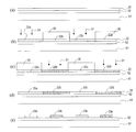
まず、基板61の上に、図3(a)を用いて説明したように、アンダーコート層62を形成した後、アンダーコート層62の上にアモルファスシリコン層22を積層して、図14(a)に示す積層構造を得る。
次に、図14(b)に示すように、a-Si層22の上にレジスト30を積層し、フォトリソグラフィ法によって領域22a(第1領域)及び22c(第3領域)の上にレジスト30の開口を設け、領域22a及び22cにBをドープする(第1回目のドーピング工程(第1工程))。
次に、レジスト30を取り除いた後、図14(c)に示すように、a-Si層22の上に再度レジスト30を積層し、領域22b(第2領域)及び22d(第4領域)の上に開口を設け、領域22b及び22dにBをドープする(第2回目のドーピング工程(第2工程))。
次に、レジスト30を除去した後、領域22a~22dにレーザアニールを施して、図14(d)に示すように、ポリシリコン層23を得る。その後、フォトリソグラフィ法によりポリシリコン層23を部分的に除去して、図14(e)に示すように、ポリシリコン領域23a~23dを得、図4(a)及び(b)を用いて説明した工程を経て、半導体装置102が完成する。
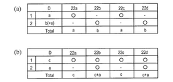
図15は、半導体装置102の半導体層20a~20dの形成における2種類のドープ処理方法を説明するための表である。
図15の(a)は、上記半導体装置102の製造方法における2回のドーピング工程(第1のドーピング例)において、領域22a~22dにドープされるBの量(D)の関係を表している。この図に示すように、第1回目のドーピングでは、領域22a及び22cに量aのBがドープされ、第2回目のドーピングでは領域22b及び22dに量aよりも多い量bのBがドープされる。その結果、領域22a~22dに対する最終的なドーズ量は、それぞれ、a、b、a、及びbとなる。チャネル領域25a~25dの不純物濃度d1、d2、d3、及びd4は、d1<d2且つd3<d4の関係を満たしている。
図15の(b)は、本実施形態の第2のドーピング例によるドーズ量(D)の関係を表している。この図に示すように、第1回目のドーピングでは、領域22a~22dに量cのBがドープされ、第2回目のドーピングでは領域22b及び22dに量aのBがドープされる。その結果、領域22a~22dに対する最終的なドーズ量は、それぞれ、c、c+a、c、及びc+aとなり、不純物濃度d1、d2、d3、及びd4は、d1<d2且つd3<d4の関係を満たす。
上記第1及び第2のドーピング例は、あくまで例示であり、実施形態3のドーピング例が上記の例に限定されるわけではない。また、上記第1及び第2のドーピング例のそれぞれにおけるaの値は互いに異なっていてよい。ただし、本実施形態においてd1、d2、d3、及びd4は、d1=d3<d2=d4の関係を満たしている。
実施形態1と同様、ドーパントにはp型不純物のみならずn型不純物を用いてもよく、d1、d2、d3、及びd4は、チャネル領域25a~25dにおけるp型不純物の濃度(濃度0の場合を含む)からn型不純物(濃度0の場合を含む)の濃度を引いた値を表すものとする。
いずれの方法にせよ、チャネル領域25a~25d(及び製造工程における領域22a~22d)にドープされるp型不純物の濃度(濃度0の場合を含む)からn型不純物(濃度0の場合を含む)の濃度を引いた値をそれぞれd1、d2、d3、及びd4とすると、d1、d2、d3、及びd4は、d1=d3<d2=d4を満たす。製造方法によっては、d1、d2、d3、及びd4が、d1=d3<d2、d1=d3<d4、d1<d2=d4、又はd3<d2=d4の関係を満たすものであってもよい。また、本発明による表示装置200の製造方法は、上記の半導体装置の製造方法を含んでいる。
本実施形態によれば、同一の基板上に形成される低電圧用TFTの閾値電圧を高電圧用TFTの閾値電圧以下に抑えるなど、それが用いられる回路毎に適切に設定することができるので、半導体装置または半導体装置を含む機器における多種多様な制御を、不必要に消費電力を増加させることなく実行することが可能となる。
本発明は、薄膜トランジスタを有するアクティブマトリクス基板を備えた液晶表示装置、有機エレクトロルミネッセンス(EL)表示装置、無機エレクトロルミネッセンス表示装置等の表示装置、あるいは様々な種類の半導体装置に好適に用いられる。
10、10a~10d TFT
20a~20d 半導体層
22 アモルファスシリコン層(a-Si層)
22a~22d 領域(シリコン層の領域)
23 ポリシリコン層
23a~23d ポリシリコン領域
25a~25d チャネル領域
26a~26d ソースコンタクト領域(第1コンタクト領域)
27a~27d ドレインコンタクト領域(第2コンタクト領域)
54 ゲート(ゲート電極)
30 レジスト
31 ドーパント
32 レーザ光
55 ゲート電極
56 ソース電極
57 ドレイン電極
61 基板(透明基板、絶縁性基板)
62 アンダーコート層
63 ゲート絶縁層(ゲート絶縁膜)
64 絶縁層(層間絶縁膜)
100、101、102 半導体装置
200 表示装置
210 TFT基板
212 ゲートドライバ(走査線駆動回路)
213 データドライバ(信号線駆動回路)
214 表示コントローラ
215、216 偏光板
220 対向基板(CF基板)
230 液晶層
240 バックライトユニット
250 画素
252 画素電極
254 走査線(ゲートバスライン)
256 信号線(データバスライン)
258 補助容量線
260 表示領域
261 電源回路
262 メモリ
264 コモンドライバ
20a~20d 半導体層
22 アモルファスシリコン層(a-Si層)
22a~22d 領域(シリコン層の領域)
23 ポリシリコン層
23a~23d ポリシリコン領域
25a~25d チャネル領域
26a~26d ソースコンタクト領域(第1コンタクト領域)
27a~27d ドレインコンタクト領域(第2コンタクト領域)
54 ゲート(ゲート電極)
30 レジスト
31 ドーパント
32 レーザ光
55 ゲート電極
56 ソース電極
57 ドレイン電極
61 基板(透明基板、絶縁性基板)
62 アンダーコート層
63 ゲート絶縁層(ゲート絶縁膜)
64 絶縁層(層間絶縁膜)
100、101、102 半導体装置
200 表示装置
210 TFT基板
212 ゲートドライバ(走査線駆動回路)
213 データドライバ(信号線駆動回路)
214 表示コントローラ
215、216 偏光板
220 対向基板(CF基板)
230 液晶層
240 バックライトユニット
250 画素
252 画素電極
254 走査線(ゲートバスライン)
256 信号線(データバスライン)
258 補助容量線
260 表示領域
261 電源回路
262 メモリ
264 コモンドライバ
Claims (34)
- それぞれが多結晶シリコンからなるチャネル領域を有する第1P型TFT、第2P型TFT、第1N型TFT、及び第2N型TFTを備え、
前記第1P型TFT、前記第2P型TFT、前記第1N型TFT、及び前記第2N型TFTのチャネル領域におけるp型不純物の濃度をそれぞれd1、d2、d3、及びd4とした場合、前記d1、d2、d3、及びd4のうちの少なくとも3つの値が互いに異なり、前記d1、d2、d3、及びd4が、
d1<d2、且つd3<d4
の関係を満たす半導体装置。 - 前記第1P型TFT及び前記第2N型TFTが高電圧駆動用のTFTであり、前記第2P型TFT及び前記第1N型TFTが、前記高電圧駆動用のTFTよりも低いソース-ドレイン電圧を制御するための低電圧駆動用TFTである、請求項1に記載の半導体装置。
- 前記d1、d2、d3、及びd4の4つの値が互いに異なっている、請求項2に記載の半導体装置。
- 前記d1、d2、d3、及びd4が、d1<d2<d3<d4の関係、又はd1<d3<d2<d4の関係を満たす、請求項3に記載の半導体装置。
- 前記d1、d2、d3、及びd4のうちの3つの値が互いに異なっており、前記d1、d2、d3、及びd4のうちの2つの値が互いに等しい、請求項2に記載の半導体装置。
- 前記d1、d2、d3、及びd4が、d1<d2=d3<d4の関係、又はd1=d3<d2<d4の関係を満たす、請求項5に記載の半導体装置。
- 前記d1、d2、d3、及びd4が、それぞれ、前記第1P型TFT、前記第2P型TFT、前記第1N型TFT、及び前記第2N型TFTのチャネル領域におけるp型不純物の濃度(濃度0の場合を含む)からn型不純物(濃度0の場合を含む)の濃度を引いた値を意味する、請求項1から6のいずれか1項に記載の半導体装置。
- 請求項1から7のいずれか1項に記載の半導体装置を含む表示装置。
- それぞれが多結晶シリコンからなるチャネル領域を有する第1P型TFT、第2P型TFT、第1N型TFT、及び第2N型TFTを備え、
前記第1P型TFT及び前記第2N型TFTが高電圧駆動用のTFTであり、前記第2P型TFT及び前記第1N型TFTが、前記高電圧駆動用のTFTよりも低いソース-ドレイン電圧を制御するための低電圧駆動用TFTであり、
前記第1P型TFT、前記第2P型TFT、前記第1N型TFT、及び前記第2N型TFTのチャネル領域におけるp型不純物の濃度をそれぞれd1、d2、d3、及びd4とした場合、前記d1、d2、d3、及びd4が、
d1=d3<d2、d1=d3<d4、d1<d2=d4、又はd3<d2=d4
の関係を満たす半導体装置。 - 前記d1、d2、d3、及びd4が、
d1=d3<d2=d4
の関係を満たす、請求項9に記載の半導体装置。 - 前記d1、d2、d3、及びd4が、それぞれ、前記第1P型TFT、前記第2P型TFT、前記第1N型TFT、及び前記第2N型TFTのチャネル領域におけるp型不純物の濃度(濃度0の場合を含む)からn型不純物(濃度0の場合を含む)の濃度を引いた値を意味する、請求項9または10に記載の半導体装置。
- 請求項9から11のいずれか1項に記載の半導体装置を含む表示装置。
- それぞれが多結晶シリコンからなるチャネル領域を有する第1P型TFT、第2P型TFT、第1N型TFT、及び第2N型TFTを備えた半導体装置の製造方法であって、
前記第1P型TFT、前記第2P型TFT、前記第1N型TFT、及び前記第2N型TFTのそれぞれのチャネル領域となる第1領域、第2領域、第3領域、及び第4領域のうちの少なくとも1つの領域に対して、第1の量の不純物を同時にドープする第1工程と、
前記第1工程の前または後に、前記第1領域、前記第2領域、前記第3領域、及び前記第4領域のうち、前記第1工程において不純物がドープされる領域の少なくとも1つを含む複数の領域に対して、前記第1の量とは異なる第2の量の不純物を同時にドープする第2工程と、を含み、
前記第1領域、前記第2領域、前記第3領域、及び前記第4領域にドープされるp型不純物の濃度をそれぞれd1、d2、d3、及びd4とした場合、前記d1、d2、d3、及びd4が、
d1<d2、且つd3<d4
の関係を満たす製造方法。 - 前記第1P型TFT及び前記第2N型TFTが高電圧駆動用のTFTであり、前記第2P型TFT及び前記第1N型TFTが、前記高電圧駆動用のTFTよりも低いソース-ドレイン電圧を制御するための低電圧駆動用TFTである、請求項13に記載の製造方法。
- 前記第1工程において、前記第1領域、前記第2領域、前記第3領域、及び前記第4領域の2つの領域に対して、前記第1の量の不純物が同時にドープされ、
前記第1工程の後に前記第2工程が実施され、
前記第2工程では、前記第1領域、前記第2領域、前記第3領域、及び前記第4領域のうち、前記第1工程において不純物がドープされた領域の1つと、前記第1工程において不純物がドープされなかった領域の1つの領域に対して、前記第1の量とは異なる第2の量の不純物が同時にドープされる、請求項14に記載の製造方法。 - 前記d1、d2、d3、及びd4の4つの値が互いに異なっている、請求項15に記載の製造方法。
- 前記d1、d2、d3、及びd4が、d1<d2<d3<d4の関係、又はd1<d3<d2<d4の関係を満たす、請求項16に記載の製造方法。
- 前記第1工程において、前記第2領域及び前記第4領域に対して、前記第1の量の不純物が同時にドープされ、
前記第2工程では、前記第3領域及び前記第4領域に対して、前記第1の量よりも多い前記第2の量の不純物が同時にドープされる、請求項17に記載の製造方法。 - 前記第1工程において、前記第3領域及び前記第4領域に対して、前記第1の量の不純物が同時にドープされ、
前記第2工程では、前記第2領域及び前記第4領域に対して、前記第1の量よりも多い前記第2の量の不純物が同時にドープされる、請求項17に記載の製造方法。 - 前記第1領域、前記第2領域、前記第3領域、及び前記第4領域に対して、第3の量の不純物をドープする第3の工程を含む、請求項18または19に記載の製造方法。
- 前記d1、d2、d3、及びd4のうちの3つの値が互いに異なっており、前記d1、d2、d3、及びd4のうちの2つの値が互いに等しい、請求項14に記載の製造方法。
- 前記d1、d2、d3、及びd4が、d1<d2=d3<d4の関係、又はd1=d3<d2<d4の関係を満たす、請求項21に記載の製造方法。
- 前記第1工程において、前記第2領域、前記第3領域、及び前記第4領域に対して、前記第1の量の不純物が同時にドープされ、
前記第2工程では、前記第4領域に対して、前記第1の量よりも多い前記第2の量の不純物がドープされる、請求項22に記載の製造方法。 - 前記第1工程において、前記第4領域に対して、前記第1の量の不純物がドープされ、
前記第2工程では、前記第2領域、前記第3領域、及び前記第4領域に対して、前記第1の量よりも多い前記第2の量の不純物が同時にドープされる、請求項22に記載の製造方法。 - 前記第1工程において、前記第1領域、前記第3領域、及び前記第4領域に対して、前記第1の量の不純物が同時にドープされ、
前記第2工程では、前記第2領域及び前記第4領域に対して、前記第1の量よりも多い前記第2の量の不純物が同時にドープされる、請求項22に記載の製造方法。 - 前記第1工程において、前記第1領域及び前記第4領域に対して、前記第1の量の不純物が同時にドープされ、
前記第2工程では、前記第2領域、前記第3領域、及び前記第4領域に対して、前記第1の量よりも多い前記第2の量の不純物が同時にドープされる、請求項22に記載の製造方法。 - さらに、前記第1領域、前記第2領域、前記第3領域、及び前記第4領域に対して、第3の量の不純物が同時にドープされる工程を含む、請求項23から26のいずれか1項に記載の製造方法。
- 前記d1、d2、d3、及びd4が、それぞれ、前記第1P型TFT、前記第2P型TFT、前記第1N型TFT、及び前記第2N型TFTのチャネル領域におけるp型不純物の濃度(濃度0の場合を含む)からn型不純物(濃度0の場合を含む)の濃度を引いた値を意味する、請求項13から27のいずれか1項に記載の製造方法。
- 請求項13から28のいずれか1項に記載の製造方法を含む表示装置の製造方法。
- それぞれが多結晶シリコンからなるチャネル領域を有する第1P型TFT、第2P型TFT、第1N型TFT、及び第2N型TFTを備えた半導体装置の製造方法であって、
前記第1P型TFT及び前記第2N型TFTが高電圧駆動用のTFTであり、前記第2P型TFT及び前記第1N型TFTが、前記高電圧駆動用のTFTよりも低いソース-ドレイン電圧を制御するための低電圧駆動用TFTであり、
前記第1P型TFTのチャネル領域となる第1領域、及び前記第1N型TFTのチャネル領域となる第3領域に対して、同時に第1の量の不純物をドープする第1工程と、
前記第2P型TFTのチャネル領域となる第2領域、及び前記第2N型TFTのチャネル領域となる第4領域に対して、同時に前記第1の量とは異なる第2の量の不純物をドープする第2工程と、を含み、
前記第1領域、前記第2領域、前記第3領域、及び前記第4領域にドープされるp型不純物の濃度をそれぞれd1、d2、d3、及びd4とした場合、前記d1、d2、d3、及びd4が、
d1=d3<d2、d1=d3<d4、d1<d2=d4、又はd3<d2=d4
の関係を満たす製造方法。 - 前記d1、d2、d3、及びd4が、d1=d3<d2=d4の関係を満たす、請求項30に記載の製造方法。
- 前記第1工程において、前記第1領域、前記第2領域、前記第3領域、及び前記第4領域に対して、前記第1の量の不純物が同時にドープされる、請求項31に記載の製造方法。
- 前記d1、d2、d3、及びd4が、それぞれ、前記第1P型TFT、前記第2P型TFT、前記第1N型TFT、及び前記第2N型TFTのチャネル領域におけるp型不純物の濃度(濃度0の場合を含む)からn型不純物(濃度0の場合を含む)の濃度を引いた値を意味する、請求項30から32のいずれか1項に記載の製造方法。
- 請求項30から33のいずれか1項に記載の製造方法を含む表示装置の製造方法。
Priority Applications (1)
| Application Number | Priority Date | Filing Date | Title |
|---|---|---|---|
| US13/643,923 US8853701B2 (en) | 2010-04-28 | 2011-03-17 | Semiconductor device, display device, and production method for semiconductor device and display device |
Applications Claiming Priority (2)
| Application Number | Priority Date | Filing Date | Title |
|---|---|---|---|
| JP2010-104459 | 2010-04-28 | ||
| JP2010104459 | 2010-04-28 |
Publications (1)
| Publication Number | Publication Date |
|---|---|
| WO2011135945A1 true WO2011135945A1 (ja) | 2011-11-03 |
Family
ID=44861266
Family Applications (1)
| Application Number | Title | Priority Date | Filing Date |
|---|---|---|---|
| PCT/JP2011/056421 Ceased WO2011135945A1 (ja) | 2010-04-28 | 2011-03-17 | 半導体装置、表示装置、並びに半導体装置及び表示装置の製造方法 |
Country Status (2)
| Country | Link |
|---|---|
| US (1) | US8853701B2 (ja) |
| WO (1) | WO2011135945A1 (ja) |
Cited By (2)
| Publication number | Priority date | Publication date | Assignee | Title |
|---|---|---|---|---|
| US20130175535A1 (en) * | 2010-04-28 | 2013-07-11 | Sharp Kabushiki Kaisha | Semiconductor device, display device, and production method for semiconductor device and display device |
| US20160020228A1 (en) * | 2013-12-26 | 2016-01-21 | Boe Technology Group Co., Ltd. | Cmos transistor and method for fabricating the same, display panel and display device |
Families Citing this family (1)
| Publication number | Priority date | Publication date | Assignee | Title |
|---|---|---|---|---|
| KR102456436B1 (ko) * | 2015-02-17 | 2022-10-20 | 삼성디스플레이 주식회사 | 유기 발광 표시 장치 |
Citations (5)
| Publication number | Priority date | Publication date | Assignee | Title |
|---|---|---|---|---|
| JPH0927553A (ja) * | 1995-07-12 | 1997-01-28 | Matsushita Electron Corp | 半導体装置の製造方法 |
| JPH114004A (ja) * | 1996-12-28 | 1999-01-06 | Hyundai Electron Ind Co Ltd | 半導体装置の製造方法 |
| JP2001284596A (ja) * | 2000-03-31 | 2001-10-12 | Toshiba Corp | 半導体装置及びその製造方法 |
| JP2004128487A (ja) * | 2002-09-10 | 2004-04-22 | Nec Corp | 薄膜半導体装置及びその製造方法 |
| JP2005340695A (ja) * | 2004-05-31 | 2005-12-08 | Hitachi Displays Ltd | 表示装置の製造方法 |
Family Cites Families (16)
| Publication number | Priority date | Publication date | Assignee | Title |
|---|---|---|---|---|
| JP3304803B2 (ja) * | 1997-02-07 | 2002-07-22 | ヤマハ株式会社 | 多電源半導体装置の製造方法 |
| JP3196714B2 (ja) * | 1998-03-05 | 2001-08-06 | 日本電気株式会社 | トリプルウェル構造の半導体集積回路の製造方法 |
| US7022556B1 (en) * | 1998-11-11 | 2006-04-04 | Semiconductor Energy Laboratory Co., Ltd. | Exposure device, exposure method and method of manufacturing semiconductor device |
| US6207510B1 (en) * | 1999-01-12 | 2001-03-27 | Lucent Technologies Inc. | Method for making an integrated circuit including high and low voltage transistors |
| JP3189819B2 (ja) * | 1999-01-27 | 2001-07-16 | 日本電気株式会社 | 半導体装置の製造方法 |
| US6693331B2 (en) * | 1999-11-18 | 2004-02-17 | Intel Corporation | Method of fabricating dual threshold voltage n-channel and p-channel MOSFETS with a single extra masked implant operation |
| JP4811895B2 (ja) * | 2001-05-02 | 2011-11-09 | ルネサスエレクトロニクス株式会社 | 半導体装置およびその製造方法 |
| US6562675B1 (en) * | 2001-08-17 | 2003-05-13 | Cypress Semiconductor Corp. | Adjustment of threshold voltages of selected NMOS and PMOS transistors using fewer masking steps |
| WO2003049188A1 (en) * | 2001-11-30 | 2003-06-12 | Renesas Technology Corp. | Semiconductor integrated circuit device and manufacturing method thereof |
| JP2006332400A (ja) * | 2005-05-27 | 2006-12-07 | Nec Corp | 薄膜半導体装置およびその製造方法 |
| US7619288B2 (en) * | 2005-05-27 | 2009-11-17 | Sharp Kabushiki Kaisha | Thin film transistor substrate, liquid crystal display device provided with such thin film transistor substrate and method for manufacturing thin film transistor substrate |
| JP5038633B2 (ja) * | 2006-02-14 | 2012-10-03 | 株式会社東芝 | 半導体装置及びその製造方法 |
| US7781768B2 (en) * | 2006-06-29 | 2010-08-24 | Semiconductor Energy Laboratory Co., Ltd. | Display device, method for manufacturing the same, and electronic device having the same |
| KR100840651B1 (ko) * | 2006-12-29 | 2008-06-24 | 동부일렉트로닉스 주식회사 | 고전압 소자의 이온주입 방법 |
| EP2518759B1 (en) * | 2009-12-25 | 2017-06-21 | Mitsubishi Gas Chemical Company, Inc. | Method for manufacturing semiconductor device using an etchant |
| US8853701B2 (en) * | 2010-04-28 | 2014-10-07 | Sharp Kabushiki Kaisha | Semiconductor device, display device, and production method for semiconductor device and display device |
-
2011
- 2011-03-17 US US13/643,923 patent/US8853701B2/en not_active Expired - Fee Related
- 2011-03-17 WO PCT/JP2011/056421 patent/WO2011135945A1/ja not_active Ceased
Patent Citations (5)
| Publication number | Priority date | Publication date | Assignee | Title |
|---|---|---|---|---|
| JPH0927553A (ja) * | 1995-07-12 | 1997-01-28 | Matsushita Electron Corp | 半導体装置の製造方法 |
| JPH114004A (ja) * | 1996-12-28 | 1999-01-06 | Hyundai Electron Ind Co Ltd | 半導体装置の製造方法 |
| JP2001284596A (ja) * | 2000-03-31 | 2001-10-12 | Toshiba Corp | 半導体装置及びその製造方法 |
| JP2004128487A (ja) * | 2002-09-10 | 2004-04-22 | Nec Corp | 薄膜半導体装置及びその製造方法 |
| JP2005340695A (ja) * | 2004-05-31 | 2005-12-08 | Hitachi Displays Ltd | 表示装置の製造方法 |
Cited By (4)
| Publication number | Priority date | Publication date | Assignee | Title |
|---|---|---|---|---|
| US20130175535A1 (en) * | 2010-04-28 | 2013-07-11 | Sharp Kabushiki Kaisha | Semiconductor device, display device, and production method for semiconductor device and display device |
| US8853701B2 (en) * | 2010-04-28 | 2014-10-07 | Sharp Kabushiki Kaisha | Semiconductor device, display device, and production method for semiconductor device and display device |
| US20160020228A1 (en) * | 2013-12-26 | 2016-01-21 | Boe Technology Group Co., Ltd. | Cmos transistor and method for fabricating the same, display panel and display device |
| US10991724B2 (en) | 2013-12-26 | 2021-04-27 | Boe Technology Group Co., Ltd. | CMOS transistor and method for fabricating the same, display panel and display device |
Also Published As
| Publication number | Publication date |
|---|---|
| US8853701B2 (en) | 2014-10-07 |
| US20130175535A1 (en) | 2013-07-11 |
Similar Documents
| Publication | Publication Date | Title |
|---|---|---|
| US10438973B2 (en) | Display device and method for manufacturing same | |
| US10895774B2 (en) | Array substrate, manufacturing method, display panel and display device | |
| US10564494B2 (en) | Array substrate circuit, array substrate, and display device | |
| KR101113394B1 (ko) | 액정표시장치의 어레이 기판 | |
| US11695016B2 (en) | Active matrix substrate and method for manufacturing same | |
| CN103081108B (zh) | 薄膜晶体管基板及其制造方法、显示装置 | |
| US11355519B2 (en) | Array substrate, manufacturing method thereof, and display device | |
| CN106920804B (zh) | 一种阵列基板、其驱动方法、显示面板及显示装置 | |
| US10361229B2 (en) | Display device | |
| WO2015194417A1 (ja) | 半導体装置 | |
| CN102881657B (zh) | 一种cmos晶体管及其制造方法 | |
| KR20150076405A (ko) | 디스플레이 장치의 정전기 방지 장치와 이의 제조 방법 | |
| CN205621414U (zh) | 静电放电电路、阵列基板和显示装置 | |
| CN108807547A (zh) | 薄膜晶体管及其制备方法、阵列基板及其制备方法 | |
| WO2011151955A1 (ja) | 半導体素子、薄膜トランジスタ基板及び表示装置 | |
| JPH1154761A (ja) | 半導体集積回路およびその作製方法 | |
| CN105161544A (zh) | 薄膜场效应晶体管及其制作方法、液晶显示器 | |
| WO2011135945A1 (ja) | 半導体装置、表示装置、並びに半導体装置及び表示装置の製造方法 | |
| US7750346B2 (en) | Semiconductor structure and method for manufacturing the same | |
| JP2006332400A (ja) | 薄膜半導体装置およびその製造方法 | |
| KR102449066B1 (ko) | 표시장치용 어레이기판 및 그 제조방법 | |
| US7180156B2 (en) | Thin-film devices and method for fabricating the same on same substrate | |
| WO2017099024A1 (ja) | アクティブマトリクス基板およびそれを備える液晶表示パネル | |
| US10802363B2 (en) | Array substrate and manufacturing method therefor, display device and driving method therefor | |
| KR101760946B1 (ko) | 박막트랜지스터 어레이기판 제조방법 |
Legal Events
| Date | Code | Title | Description |
|---|---|---|---|
| 121 | Ep: the epo has been informed by wipo that ep was designated in this application |
Ref document number: 11774729 Country of ref document: EP Kind code of ref document: A1 |
|
| NENP | Non-entry into the national phase |
Ref country code: DE |
|
| WWE | Wipo information: entry into national phase |
Ref document number: 13643923 Country of ref document: US |
|
| 122 | Ep: pct application non-entry in european phase |
Ref document number: 11774729 Country of ref document: EP Kind code of ref document: A1 |
|
| NENP | Non-entry into the national phase |
Ref country code: JP |