WO2011125677A1 - 固体撮像素子及び撮像装置 - Google Patents
固体撮像素子及び撮像装置 Download PDFInfo
- Publication number
- WO2011125677A1 WO2011125677A1 PCT/JP2011/057900 JP2011057900W WO2011125677A1 WO 2011125677 A1 WO2011125677 A1 WO 2011125677A1 JP 2011057900 W JP2011057900 W JP 2011057900W WO 2011125677 A1 WO2011125677 A1 WO 2011125677A1
- Authority
- WO
- WIPO (PCT)
- Prior art keywords
- solid
- imaging device
- state imaging
- photoelectric conversion
- readout circuit
- Prior art date
- Legal status (The legal status is an assumption and is not a legal conclusion. Google has not performed a legal analysis and makes no representation as to the accuracy of the status listed.)
- Ceased
Links
Images



Classifications
-
- H—ELECTRICITY
- H04—ELECTRIC COMMUNICATION TECHNIQUE
- H04N—PICTORIAL COMMUNICATION, e.g. TELEVISION
- H04N25/00—Circuitry of solid-state image sensors [SSIS]; Control thereof
- H04N25/60—Noise processing, e.g. detecting, correcting, reducing or removing noise
- H04N25/63—Noise processing, e.g. detecting, correcting, reducing or removing noise applied to dark current
- H04N25/633—Noise processing, e.g. detecting, correcting, reducing or removing noise applied to dark current by using optical black pixels
-
- H—ELECTRICITY
- H04—ELECTRIC COMMUNICATION TECHNIQUE
- H04N—PICTORIAL COMMUNICATION, e.g. TELEVISION
- H04N25/00—Circuitry of solid-state image sensors [SSIS]; Control thereof
- H04N25/70—SSIS architectures; Circuits associated therewith
- H04N25/76—Addressed sensors, e.g. MOS or CMOS sensors
- H04N25/77—Pixel circuitry, e.g. memories, A/D converters, pixel amplifiers, shared circuits or shared components
-
- H—ELECTRICITY
- H10—SEMICONDUCTOR DEVICES; ELECTRIC SOLID-STATE DEVICES NOT OTHERWISE PROVIDED FOR
- H10F—INORGANIC SEMICONDUCTOR DEVICES SENSITIVE TO INFRARED RADIATION, LIGHT, ELECTROMAGNETIC RADIATION OF SHORTER WAVELENGTH OR CORPUSCULAR RADIATION
- H10F39/00—Integrated devices, or assemblies of multiple devices, comprising at least one element covered by group H10F30/00, e.g. radiation detectors comprising photodiode arrays
- H10F39/10—Integrated devices
- H10F39/12—Image sensors
-
- H—ELECTRICITY
- H10—SEMICONDUCTOR DEVICES; ELECTRIC SOLID-STATE DEVICES NOT OTHERWISE PROVIDED FOR
- H10F—INORGANIC SEMICONDUCTOR DEVICES SENSITIVE TO INFRARED RADIATION, LIGHT, ELECTROMAGNETIC RADIATION OF SHORTER WAVELENGTH OR CORPUSCULAR RADIATION
- H10F39/00—Integrated devices, or assemblies of multiple devices, comprising at least one element covered by group H10F30/00, e.g. radiation detectors comprising photodiode arrays
- H10F39/80—Constructional details of image sensors
- H10F39/805—Coatings
- H10F39/8057—Optical shielding
-
- H—ELECTRICITY
- H10—SEMICONDUCTOR DEVICES; ELECTRIC SOLID-STATE DEVICES NOT OTHERWISE PROVIDED FOR
- H10F—INORGANIC SEMICONDUCTOR DEVICES SENSITIVE TO INFRARED RADIATION, LIGHT, ELECTROMAGNETIC RADIATION OF SHORTER WAVELENGTH OR CORPUSCULAR RADIATION
- H10F39/00—Integrated devices, or assemblies of multiple devices, comprising at least one element covered by group H10F30/00, e.g. radiation detectors comprising photodiode arrays
- H10F39/10—Integrated devices
- H10F39/12—Image sensors
- H10F39/18—Complementary metal-oxide-semiconductor [CMOS] image sensors; Photodiode array image sensors
-
- H—ELECTRICITY
- H10—SEMICONDUCTOR DEVICES; ELECTRIC SOLID-STATE DEVICES NOT OTHERWISE PROVIDED FOR
- H10F—INORGANIC SEMICONDUCTOR DEVICES SENSITIVE TO INFRARED RADIATION, LIGHT, ELECTROMAGNETIC RADIATION OF SHORTER WAVELENGTH OR CORPUSCULAR RADIATION
- H10F39/00—Integrated devices, or assemblies of multiple devices, comprising at least one element covered by group H10F30/00, e.g. radiation detectors comprising photodiode arrays
- H10F39/80—Constructional details of image sensors
- H10F39/803—Pixels having integrated switching, control, storage or amplification elements
- H10F39/8037—Pixels having integrated switching, control, storage or amplification elements the integrated elements comprising a transistor
Definitions
- the present invention relates to a solid-state imaging device and an imaging apparatus.
- a conventional CCD type or CMOS type image sensor (solid-state imaging device) generally used is a light receiving unit (consisting of a plurality of photoelectric conversion units arranged in a two-dimensional array on the surface of a semiconductor substrate ( An effective pixel region portion) is provided, and a subject image signal corresponding to a subject light image formed on the light receiving portion is output from each photoelectric conversion portion.
- An optical black (OB) portion covered with a light shielding film is provided around the light receiving portion, and a dark signal output from the OB portion is output as a reference signal from the light receiving portion. The offset component of the subject image signal is removed.
- the minute subject image signal from the light receiving unit can be obtained with high accuracy. It becomes possible to detect, and it is possible to achieve a high S / N ratio of the solid-state imaging device. Since the dark output changes depending on the environment such as temperature, an OB pixel equivalent to an effective pixel is created, and a difference between the outputs is used as a subject image signal, so that a high S / N subject image signal can be obtained in any environment. can get.
- the above-described conventional CCD or CMOS type solid-state imaging device has a photoelectric conversion unit (photodiode) on a semiconductor substrate and a signal readout circuit (CCD type) that reads an object image signal detected by the photoelectric conversion unit to the outside.
- a photoelectric conversion unit photodiode
- CCD type signal readout circuit
- a charge transfer path, an output amplifier, and a MOS transistor circuit in the case of a CMOS type must be formed on the same semiconductor substrate surface portion.
- the aperture ratio that the ratio which the photoelectric conversion part accounts to the chip area of a solid-state image sensor cannot be made into 100%. In recent years, this aperture ratio tends to decrease with the miniaturization of pixels, and has become a factor for reducing S / N.
- a solid-state solid-state imaging device having a structure in which only a signal readout circuit is provided on the semiconductor substrate without providing a photoelectric conversion portion on the surface of the semiconductor substrate and a photoelectric conversion layer is stacked above the semiconductor substrate is attracting attention. It is becoming.
- the solid-state imaging device described in Patent Document 1 is configured to detect X-rays and electron beams by performing photoelectric conversion with amorphous silicon or the like laminated above a semiconductor substrate.
- a photoelectric conversion layer is shielded by stacking a 2 ⁇ m thick light-shielding layer around the effective pixel region (light receiving portion) on the outermost surface of the solid-state image sensor, and the black level of the effective pixel is set.
- OB pixels are used for detection.
- the solid-state imaging device described in Patent Document 2 includes three photoelectric conversion layers, a red detection photoelectric conversion layer, a green detection photoelectric conversion layer, and a blue detection photoelectric conversion layer. An image is taken.
- this solid-state imaging device only a light shielding film is laminated between the semiconductor substrate surface and the lowermost photoelectric conversion film so that light does not enter the signal readout circuit, and the configuration of the OB portion is particularly considered. Not done.
- Patent Documents 3 and 4 there are some which are described in Patent Documents 3 and 4 as stacked solid-state imaging devices using a glass substrate or the like instead of a semiconductor substrate.
- Patent Document 3 has a configuration in which a photoelectric conversion film is stacked on a substrate on which a TFT circuit is formed, and wiring connected to the TFT circuit of the effective pixel is provided around the effective pixel. And a noise removing pixel for removing fluctuations of the signal line. Patent Document 3 only describes a pixel for noise removal that removes noise on wiring and signal lines, and does not consider the OB pixel.
- the solid-state imaging device described in Patent Document 4 has a configuration in which an OB pixel is provided for each effective pixel, and the OB pixel has a dummy capacitance having a capacity equivalent to that of a photoelectric conversion element included in the effective pixel;
- the TFT circuit includes the TFT circuit having the same capacity as the TFT circuit included in the effective pixel.
- a configuration of the OB pixel and the effective pixel a configuration in which the dummy capacitance of the OB pixel and the photoelectric conversion element of the effective pixel are formed in the same layer, and a dummy capacitance of the OB pixel are included in the photoelectric conversion element of the effective pixel.
- the structure formed below is described.
- a light-shielding film provided in the OB portion is stacked with a thickness of 2 ⁇ m, so that a step of 2 ⁇ m is generated between the OB portion and the light receiving portion. Therefore, if light enters the stepped portion and is irregularly reflected, the subject image may be degraded. Further, since the light shielding film is provided on the photoelectric conversion film, the number of processes and the cost are increased.
- the solid-state imaging device described in Patent Document 4 has a structure having an OB pixel for each pixel. In this case, after patterning the photoelectric conversion film for each pixel, it is necessary to stack a light shielding film or install a dummy pixel. For this reason, the number of processes and cost increase.
- a general solid-state imaging device has a structure in which an OB pixel is provided around an effective pixel, and it is necessary to develop an OB pixel suitable for this.
- An object of the present invention is to provide a stacked solid-state imaging device and an imaging apparatus capable of obtaining a high-quality, high S / N captured image signal.
- the solid-state imaging device of the present invention has a solid pixel having an effective pixel including a photoelectric conversion element and an OB pixel provided outside the region where the effective pixel is formed and for obtaining a dark output of the photoelectric conversion element.
- the photoelectric conversion element is configured to include a pair of electrodes provided above a semiconductor substrate, and a light receiving layer provided between the pair of electrodes, and the light receiving layer includes all of the light receiving layers.
- a first signal readout circuit that includes a MOS transistor that is shared by effective pixels, and that is formed on the semiconductor substrate and that reads out a signal corresponding to the charge generated by the photoelectric conversion element.
- the OB pixel is connected to a second signal readout circuit formed on the semiconductor substrate having the same configuration as the first signal readout circuit, and an input node of the first signal readout circuit
- the capacitor is provided closer to the semiconductor substrate than the photoelectric conversion element, and the first signal readout circuit, the second signal readout circuit, and the capacitor are more than the photoelectric conversion element.
- the light shielding layer formed on the semiconductor substrate side shields light, and the input node of the first signal readout circuit is electrically connected to one of the pair of electrodes of the photoelectric conversion element,
- the input node of the second signal readout circuit is connected to the capacitor, and the capacitance value of the capacitor is the capacitance at the input node of the first signal readout circuit and the input of the second signal readout circuit.
- the capacitance at the node is a value that is substantially equivalent.
- a signal equal to the dark output signal of the effective pixel can be obtained from the second signal readout circuit of the OB pixel, and a high-quality captured image signal from which the dark output noise of the effective pixel is removed can be obtained.
- an effective pixel can be formed because a signal equal to the dark output signal of the effective pixel can be obtained without forming a light shielding layer on the outermost surface of the region where the OB pixel is formed. It is possible to prevent image quality deterioration due to a step between the region and the region where the OB pixel is formed.
- the imaging device of the present invention includes the solid-state imaging device.
- the present invention it is possible to provide a stacked solid-state imaging device and an imaging apparatus capable of obtaining a high-quality, high S / N captured image signal.
- FIG. 1 is a schematic plan view showing a schematic configuration of a stacked solid-state imaging device for explaining an embodiment of the present invention.
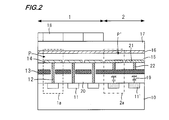
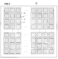
- 1 is a schematic cross-sectional view taken along line AA in the solid-state imaging device 100 shown in FIG. 2 is a schematic plan view showing the arrangement of effective pixels and OB pixels included in the solid-state imaging device 100 shown in FIG.
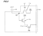
- FIG. 3 is a diagram showing an example of a circuit configuration of the signal readout circuit 11 shown in FIG.
- the figure which shows an example of the circuit structure of the signal read-out circuit 11 'shown in FIG. It is a figure which shows the 1st modification of the solid-state image sensor shown in FIG. 1, and is a figure corresponding to FIG.
- FIG. 1 is a schematic plan view showing a schematic configuration of a stacked solid-state imaging device 100 for explaining an embodiment of the present invention.
- the solid-state imaging device 100 is used as an imaging device for an imaging module mounted on an imaging device such as a digital camera or a digital video camera, an electronic endoscope, a mobile phone with a camera, or the like.
- 1 includes an effective pixel region 1, an OB pixel region 2 formed around the effective pixel region 1, and a control circuit 3.
- the effective pixel area 1 is an area in which effective pixels for obtaining a signal corresponding to the subject light are two-dimensionally arranged. As will be described in detail later, this effective pixel is composed of a photoelectric conversion element formed above the semiconductor substrate and a signal readout circuit provided corresponding to this photoelectric conversion element.
- the OB pixel area 2 is an area in which at least one OB pixel for obtaining a dark output signal output from the effective pixel in a state where light is not incident on the effective pixel is arranged.
- the OB pixel includes a dummy photoelectric conversion element that does not perform signal readout, and a signal readout circuit that is provided corresponding to the dummy photoelectric conversion element.
- the effective pixels in the effective pixel region 1 and the OB pixels in the OB pixel region 2 are arranged in a two-dimensional shape (for example, a square lattice shape) as a whole in plan view.
- the control circuit 3 performs driving for reading signals from the effective pixels and the OB pixels.
- the control circuit 3 also performs processing for correcting the black level by subtracting the signal read from the OB pixel from the signal read from the effective pixel.
- FIG. 2 is a schematic cross-sectional view taken along line AA in the solid-state imaging device 100 shown in FIG.
- FIG. 3 is a schematic plan view showing an arrangement of effective pixels and OB pixels included in the solid-state imaging device 100 shown in FIG.
- a plurality of effective pixels 1 a (only a part of the effective pixels 1 a are denoted by reference numerals in FIGS. 2 and 3) are formed in the effective pixel region 1, and a plurality of effective pixels 1 a are formed in the surrounding OB pixel region 2.
- the OB pixel 2a (only a part of the OB pixel 2a is attached in FIGS. 2 and 3) is formed.
- an insulating layer 20 is formed on the semiconductor substrate 10 in a region where the effective pixel region 1 and the OB pixel region 2 are combined.
- the pixel electrode 14 and the pixel electrode 21 are formed two-dimensionally arranged at a constant pitch in a plan view shown in FIG. .
- the pixel electrode 14 is disposed in the effective pixel region 1, and the pixel electrode 21 is disposed in the OB pixel region 2.
- the pixel electrode 14 and the pixel electrode 21 are formed by forming an electrode material on the insulating layer 20 and then patterning the electrode material, and are formed in the same layer.
- the light receiving layer 15 common to all the pixels is formed on the pixel electrode 14 and the pixel electrode 21 so as to cover them.
- a counter electrode 16 is formed on the light receiving layer 15, and a protective layer 17 is formed on the counter electrode 16.
- a color filter 18 is formed on the protective layer 17 in the effective pixel region 1 at a position facing each pixel electrode 14 in the effective pixel region 1.
- the color filter 18 is, for example, a primary color filter arranged in a Bayer array.
- the photoelectric conversion element P of the effective pixel 1a is formed by the pixel electrode 14 in the effective pixel region 1, the upper counter electrode 16, and the light receiving layer 15 therebetween.
- a dummy photoelectric conversion element P ′ of the OB pixel 2 a is formed by the pixel electrode 21 in the OB pixel region 2, the upper counter electrode 16, and the light receiving layer 15 therebetween.
- the light receiving layer 15 includes at least a photoelectric conversion layer configured to include an organic or inorganic photoelectric conversion material that generates an electric charge according to received light.
- the photoelectric conversion layer uses a photoelectric conversion material having sensitivity to visible light.
- the counter electrode 16 is an electrode for applying a bias voltage between the pixel electrodes 14 and 21 and the counter electrode 16, and a voltage is supplied from a power source (not shown). By applying a bias voltage between the pixel electrodes 14 and 21 and the counter electrode 16, charges generated in the light receiving layer 15 of the photoelectric conversion elements P and P ′ can be moved to the pixel electrodes 14 and 21.
- the counter electrode 16 is made of a material that is transparent to incident light in order to allow light to enter the light receiving layer 15.
- a transparent conductive oxide (TCO) having a high visible light transmittance and a low resistance value can be used.
- the pixel electrodes 14 and 21 are electrodes for collecting charges generated in the light receiving layer 15 of the photoelectric conversion elements P and P ′ including the pixel electrodes 14 and 21.
- the pixel electrodes 14 and 21 are made of a transparent or opaque conductive material.
- a metal such as Cr, In, Al, Ag, W, TiN (titanium nitride), or TCO can be used.
- the light receiving layer 15 may be provided with a charge blocking layer for preventing charges from being injected from the pixel electrodes 14 and 21 into the photoelectric conversion layer between the pixel electrodes 14 and 21 and the photoelectric conversion layer.
- a charge blocking layer for preventing charge from being injected from the counter electrode 16 into the photoelectric conversion layer may be provided between the counter electrode 16 and the photoelectric conversion layer.
- the light receiving layer 15 may be provided with other functional layers other than the charge blocking layer.
- a signal readout circuit 11 provided corresponding to each photoelectric conversion element P is formed on the semiconductor substrate 10 in the effective pixel region 1.
- the photoelectric conversion element P and the signal readout circuit 11 constitute an effective pixel 1a.
- the signal readout circuit 11 of the effective pixel 1a is electrically connected to the pixel electrode 14 of the effective pixel 1a via the conductive plug 12 formed in the insulating layer 20. That is, the signal readout circuit 11 of the effective pixel 1a is electrically connected to the light receiving layer 15 of the photoelectric conversion element P of the effective pixel 1a.
- the signal readout circuit 11 ′ has the same circuit configuration as the signal readout circuit 11, but its input node is not electrically connected to the photoelectric conversion elements P and P ′ and is connected to a capacitor (capacitance) 19. ing.
- the capacitor 19 is formed in the insulating layer 20 that is closer to the semiconductor substrate 10 than the photoelectric conversion element P.
- the input node of the signal readout circuit 11 ′ is electrically connected to one end of the capacitor 19.
- the OB pixel 2a is configured by the photoelectric conversion element P ', the signal readout circuit 11' corresponding to the photoelectric conversion element P ', and the capacitor 19 connected thereto.
- the capacitor 19 included in the OB pixel 2a is formed in the insulating layer 20 between the semiconductor substrate 10 and the light shielding layer 13 in the example of FIG.
- a light shielding layer 13 is formed in the insulating layer 20.
- the light shielding layer 13 is formed above the semiconductor substrate 10 and below the photoelectric conversion elements P and P ′, and shields the signal readout circuit 11, the signal readout circuit 11 ′, and the capacitor 19.
- the light shielding layer 13 is made of an opaque material (tungsten, aluminum, etc.) made of, for example, metal.
- the light shielding layer 13 is connected to a power supply terminal (not shown) to which a fixed power supply (for example, ground) is connected.
- the pixel electrode 21 of the OB pixel 2 a is electrically connected to the light shielding layer 13 through a conductive plug 22 formed in the insulating layer 20. For this reason, the charges generated in the light receiving layer 15 of the photoelectric conversion element P ′ and collected in the pixel electrode 21 are discharged from the light shielding layer 13 to the fixed power source.
- the light shielding film is not formed above the counter electrode 16 in the OB pixel region 2. For this reason, in the effective pixel region 1 and the OB pixel region 2, there is no step in the layer below the color filter 18.
- FIG. 4 is a diagram showing an example of the circuit configuration of the signal readout circuit 11 shown in FIG.
- the signal readout circuit 11 has a known three-transistor configuration including a floating diffusion FD that is an input node, a reset transistor 11a, an output transistor 11b, and a row selection transistor 11c.
- the floating diffusion FD is electrically connected to the pixel electrode 14 via the conductive plug 12, and its potential changes according to the potential of the pixel electrode 14.
- the reset transistor 11a is a MOS transistor that resets the potential of the floating diffusion FD.
- the reset transistor 11a is controlled by the control circuit 3.
- the output transistor 11b is a MOS transistor that outputs a signal corresponding to the potential of the floating diffusion FD.
- the row selection transistor 11c is a MOS transistor that outputs the signal converted by the output transistor 11b to the output signal line 11d when the row selection pulse RW is supplied from the control circuit 3 to the gate electrode.
- FIG. 5 is a diagram illustrating an example of a circuit configuration of the signal readout circuit 11 ′ illustrated in FIG. 2.
- the signal readout circuit 11 ′ is the same as the signal readout circuit 11 shown in FIG. 4 except that one end of the capacitor 19 instead of the pixel electrode 14 is electrically connected to the floating diffusion FD that is an input node. It is a configuration.
- the capacitance value of the capacitor 19 is the capacitance at the input node of the signal readout circuit 11 (total capacitance including the capacitance of the photoelectric conversion element P, the capacitance of the signal readout circuit 11 itself, and other parasitic capacitances).
- the capacitance at the input node of the signal readout circuit 11 ′ (capacitance of the capacitor 19, the capacitance of the signal readout circuit 11 ′ itself, and the total capacitance including other parasitic capacitances) is substantially the same. It is a capacity value.
- the signal readout circuit 11 ′ is a component formed in the semiconductor substrate 10 (for example, a transistor source, drain, floating diffusion FD, etc.) and a gate insulating film (not shown) on the semiconductor substrate. It is comprised with an element (for example, the gate electrode etc. of a transistor).
- the insulating layer 20 is a layer formed on the gate electrode, and wiring such as a signal output line and a power supply line connected to the signal readout circuit 11 ′ is formed in the insulating layer 20.
- the capacitor 19 is formed in the insulating layer 20. That is, the capacitor 19 is formed above the semiconductor substrate 10.
- the capacitor 19 Since the capacitor 19 is above the semiconductor substrate 10, the characteristics of the signal readout circuit 11 and the signal readout circuit 11 'can be easily matched. As a result, the capacitor 19 can be easily designed, leading to cost reduction.
- the signal read out from the signal readout circuit 11 ′ to the output signal line 11d is output in the dark state of the photoelectric conversion element P connected to the signal readout circuit 11 if the dark current generated in the light receiving layer 15 is negligibly small. This is equivalent to the signal (output signal in the dark). That is, a signal equal to the dark output signal of the effective pixel 1a can be read from the OB pixel 2a.
- the effective pixel 1a and the OB pixel 2a are only equivalent in circuit, it is difficult for the OB pixel 2a to detect a change in dark current generated in the photoelectric conversion element P. For this reason, it is preferable to use the light receiving layer 15 that is so small that the change in dark current due to temperature is negligible (the environmental dependence is negligibly small).
- the light receiving layer 15 includes an organic material so that the environmental dependency of the light receiving layer 15 can be ignored.
- the light receiving layer 15 has a multi-layer structure including a photoelectric conversion layer containing an organic material and a charge blocking layer containing an organic material because the dark current reduction effect is high.
- the capacitance value at the input node of the signal readout circuit 11 and the capacitance value at the input node of the signal readout circuit 11 ′ are substantially equal to each other. This means that the difference in capacitance value at the input node of the readout circuit 11 ′ is within 10% at room temperature (25 ° C.). Preferably, the difference is within 3%, more preferably the difference is within 1%.
- the error is within 10%, it is possible to remove main noise that greatly reduces the image quality. If the error is within 3%, almost all noise can be removed. If the error is within 1%, the noise can be completely removed.
- the capacitance value of the photoelectric conversion element P can be calculated in the same manner as a general dielectric material from the dielectric constant and thickness of the light receiving layer 15 and the size of the pixel electrode 14. Further, the capacitance value at the input node of the signal readout circuit 11, 11 'can be measured by the optical shot noise method.
- a capacitor 19 having a small environmental dependency it is preferable to use an MM (metal-metal) type capacitor having an insulating layer sandwiched between metals and a PIP (poly-poly) type capacitor having an insulating layer sandwiched between polysilicon. This is because if the environment dependency is large, a signal equal to the dark output of the effective pixel 1a may not always be read from the OB pixel 2a.
- signal readout is started from the effective pixel 1a and the OB pixel 2a.
- the control circuit 3 sequentially turns on the row selection transistor 11c of the signal readout circuit 11 to output a signal corresponding to the potential of the floating diffusion FD of the signal readout circuit 11 to the output signal line 11d.
- a signal (hereinafter referred to as an effective signal) output to the output signal line 11d is stored in a memory of an imaging device on which the solid-state imaging device 100 is mounted.
- the control circuit 3 sequentially turns on the row selection transistor 11c of the signal readout circuit 11 ′, so that a signal corresponding to the potential of the floating diffusion FD of the signal readout circuit 11 ′ (hereinafter referred to as an OB signal). ) To the output signal line 11d.
- the OB signal output to the output signal line 11d is stored in the memory of the image pickup apparatus on which the solid-state image pickup device 100 is mounted.
- the imaging apparatus obtains a subject image signal from which the influence of dark output is eliminated by performing black level correction processing in which the OB signal is subtracted from each valid signal stored in the memory.
- an OB signal equal to the dark output signal in a state where the photoelectric conversion element P is shielded from light can be read by the signal reading circuit 11 ′ of the OB pixel 2a.
- An S / N subject image signal can be obtained.
- an OB signal can be acquired without providing a light shielding film above the counter electrode 16 in the OB pixel region 2. For this reason, there is no step caused by the light-shielding film in the effective pixel region 1 and the OB pixel region 2, and there is no possibility that the subject image is deteriorated due to irregular reflection of light. In addition, since it is not necessary to form a light shielding film above the counter electrode 16, the cost required for the process of forming the light shielding film can be reduced.
- the signal readout circuit 11 ′ and the capacitor 19 can be shielded by using this light-shielding layer. An increase in the manufacturing process can be prevented.
- a dummy photoelectric conversion element P ′ is formed in the OB pixel region 2.
- the solid-state imaging device 100 can be easily manufactured by forming the photoelectric conversion element P ′ in the OB pixel region 2.
- the dummy photoelectric conversion element P ′ is an element that does not perform signal readout and is not used for imaging (element that is not electrically connected to the signal readout circuits 11 and 11 ′), and thus the pixel electrode 21 is omitted. May be. Since the pixel electrode 21 is formed simultaneously with the pixel electrode 14, the presence or absence of the pixel electrode 21 does not affect the manufacturing.
- the outermost pixel electrode 14 among the plurality of pixel electrodes 14 arranged in the effective pixel region 1 is the OB pixel region.
- the level of the signal from the outermost effective pixel 1a out of the plurality of effective pixels 1a increases, and the image quality may deteriorate. Therefore, when the pixel electrode 21 of the dummy photoelectric conversion element P ′ is omitted, image quality deterioration can be prevented by performing processing that does not use the signal read from the outermost effective pixel 1a.
- image data can be generated without performing processing that does not use a signal read from the outermost effective pixel 1a.
- the pixel electrode 14 and the pixel electrode 21 are made of a light-shielding material, so that the light-shielding properties of the signal readout circuits 11, 11 ′ and the capacitor 19 can be improved. .
- the color filter 18 is not formed in the OB pixel region 2, but the color filter 18 may be formed here. In this case, the amount of light incident on the light shielding layer 13 in the OB pixel region 2 can be reduced, and unnecessary light reflection in the insulating layer 20 can be reduced.
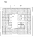
- FIG. 6 is a diagram illustrating a first modification of the solid-state imaging device illustrated in FIG. 1, and corresponds to FIG.
- the solid-state imaging device shown in FIG. 6 is shown in FIG. 3 except that the pixel electrode 21 in the OB pixel region 2 is integrally formed over all the OB pixels without partitioning the OB pixels 2a.
- the configuration is the same.
- the pixel electrode 21 may not be divided for each OB pixel 2 a. Therefore, no problem occurs even if the pixel electrode 21 of the OB pixel 2a is integrated in the entire OB pixel region 2 as shown in FIG.
- FIG. 7 is a diagram showing a modification of the signal readout circuit 11 in the solid-state imaging device shown in FIG.
- the signal readout circuit 11 shown in FIG. 7 has the same configuration as the circuit shown in FIG. 4 except that a transistor 11e, a charge storage unit 11f, a transistor 11g, and a connection unit 11h that is an input node are added. It is.
- the charge accumulating portion 11f is an impurity layer formed in the semiconductor substrate 10 and accumulates charges collected by the pixel electrode 14 of the photoelectric conversion element P.
- the transistor 11e is an impurity layer formed in the semiconductor substrate 10 at a slight distance from the charge storage unit 11f, and is electrically connected to the pixel electrode 14 via the conductive plug 12.
- a potential barrier portion made of an impurity layer forming a potential barrier is formed below the gate electrode of the transistor 11e.
- the charges collected by the pixel electrode 14 during the exposure reach the connection portion 11h via the conductive plug 12, and are accumulated in the charge accumulation portion 11f from here through the potential barrier portion.
- the transistor 11g is a transistor having a charge storage portion 11f, a floating diffusion FD, and a gate electrode above the semiconductor substrate 10 therebetween, and the charge stored in the charge storage portion 11f is controlled by controlling the voltage of the gate electrode. Is transferred to the floating diffusion FD.
- the signal readout circuit 11 may be configured to temporarily store the charge generated in the photoelectric conversion element P in the charge storage unit 11f in the semiconductor substrate 10 and then convert the charge into a signal.
- Such a circuit configuration is described in detail in Japanese Patent Application Laid-Open No. 2010-16417.
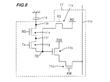
- FIG. 8 is a diagram showing a modified example of the signal readout circuit 11 ′ in the solid-state imaging device shown in FIG. 1.
- the signal readout circuit 11 'shown in FIG. 8 has the same configuration as the circuit shown in FIG. 7 except that the capacitor 19 is connected to the connection portion 11h of the transistor 11e.
- the signal readout circuit 11 and the signal readout circuit 11 ′ have the same configuration, and the capacitance values at the respective input nodes (connection portions 11h) are made substantially equal, so that the photoelectric conversion is performed from the signal readout circuit 11 ′.
- a signal equal to the signal obtained in the dark state of the element P can be obtained.
- the capacitor 19 is under the light shielding layer 13, but the capacitor 19 may be formed in the insulating layer 20 on the light shielding layer 13.
- a light shielding layer for shielding the capacitor 19 may be separately formed in the insulating layer 20. Even in this case, an OB signal can be acquired without forming a light-shielding film above the counter electrode 16, so that image quality can be improved.
- the disclosed solid-state imaging device has a solid pixel having an effective pixel including a photoelectric conversion element, and an OB pixel provided outside the region where the effective pixel is formed and for obtaining a dark output of the photoelectric conversion element.
- the photoelectric conversion element is configured to include a pair of electrodes provided above a semiconductor substrate, and a light receiving layer provided between the pair of electrodes, and the light receiving layer includes all of the light receiving layers.
- a first signal readout circuit that includes a MOS transistor that is shared by effective pixels, and that is formed on the semiconductor substrate and that reads out a signal corresponding to the charge generated by the photoelectric conversion element.
- the OB pixel includes a second signal readout circuit formed on the semiconductor substrate having the same configuration as the first signal readout circuit, and an input node of the first signal readout circuit.
- the capacitor is provided closer to the semiconductor substrate than the photoelectric conversion element, and the first signal readout circuit, the second signal readout circuit, and the capacitor are more than the photoelectric conversion element.
- the light shielding layer formed on the semiconductor substrate side shields light, and the input node of the first signal readout circuit is electrically connected to one of the pair of electrodes of the photoelectric conversion element,
- the input node of the second signal readout circuit is connected to the capacitor, and the capacitance value of the capacitor is the capacitance value of the input node of the first signal readout circuit and the second signal readout circuit.
- the capacitance value at the input node is substantially the same.
- the light receiving layer has a photoelectric conversion layer containing an organic material.
- the light-receiving layer has a charge blocking layer containing an organic material.
- the capacitor is formed above the semiconductor substrate.
- the electrode of the capacitor is made of metal or polysilicon.
- the disclosed solid-state imaging device has a dummy photoelectric conversion element in which the OB pixel is provided above the semiconductor substrate and is not electrically connected to the second signal readout circuit.
- the element includes at least an electrode formed in the same layer as the other of the pair of electrodes of the photoelectric conversion element and the light receiving layer.
- a light-shielding film is not formed above the electrode formed in the same layer as the other electrode of the dummy photoelectric conversion device.
- the disclosed solid-state imaging device includes a charge discharging unit that discharges charges generated in the light receiving layer of the dummy photoelectric conversion element.
- the dummy photoelectric conversion element includes the electrode formed in the same layer as the other electrode, the light receiving layer, and a dummy electrode formed in the same layer as the one electrode.
- a power supply terminal is connected to the light shielding layer, the dummy electrode is electrically connected to the light shielding layer, and the charge discharging unit is constituted by the dummy electrode, the light shielding layer, and the power supply terminal. is there.
- the disclosed solid-state imaging device has a plurality of the OB pixels, and the dummy electrodes are integrally formed over all the OB pixels.
- the first signal readout circuit accumulates charges collected by the one electrode in the semiconductor substrate and accumulated in the charge accumulation unit. It includes a floating diffusion to which charges are transferred and a transistor circuit that outputs a signal corresponding to the potential of the floating diffusion.
- the first signal readout circuit includes a floating diffusion connected to the one electrode and a transistor circuit that outputs a signal corresponding to the potential of the floating diffusion.
- the disclosed imaging device includes the solid-state imaging device.
- the present invention it is possible to provide a stacked solid-state imaging device and an imaging apparatus capable of obtaining a high-quality, high S / N captured image signal.
Landscapes
- Engineering & Computer Science (AREA)
- Multimedia (AREA)
- Signal Processing (AREA)
- Solid State Image Pick-Up Elements (AREA)
- Transforming Light Signals Into Electric Signals (AREA)
Abstract
Description
図6は、図1に示した固体撮像素子の第一の変形例を示す図であり、図3に対応する図である。図6に示した固体撮像素子は、OB画素領域2にある画素電極21をOB画素2a毎に区画せずに、全てのOB画素に渡って一体的に形成した点以外は、図3に示した構成と同じである。
図7は、図1に示した固体撮像素子における信号読み出し回路11の変形例を示す図である。
本出願は、2010年3月31日出願の日本出願(特願2010-084408)及び2010年10月29日出願の日本出願(特願2010-244819)に基づくものであり、その内容はここに参照として取り込まれる。
2 OB画素領域
1a 有効画素
2a OB画素
10 半導体基板
11,11’ 信号読み出し回路
13 遮光層
14 画素電極
15 光電変換層
16 対向電極
19 キャパシタ
20 絶縁層
21 ダミーの画素電極
P 光電変換素子
P’ ダミーの光電変換素子
Claims (13)
- 光電変換素子を含む有効画素と、前記有効画素が形成される領域の外側に設けられ、前記光電変換素子の暗時出力を取得するためのOB画素とを有する固体撮像素子であって、
前記光電変換素子は、半導体基板上方に設けられた一対の電極と、前記一対の電極の間に設けられた受光層とを含んで構成され、
前記受光層は全ての前記有効画素で共通化されており、
前記有効画素は、前記半導体基板に形成され、前記光電変換素子で発生した電荷に応じた信号を読み出す、MOSトランジスタを含んで構成された第一の信号読み出し回路を含み、
前記OB画素は、前記第一の信号読み出し回路と同じ構成の前記半導体基板に形成された第二の信号読み出し回路、及び、前記第一の信号読み出し回路の入力ノードに接続されたキャパシタを含み、
前記キャパシタは、前記光電変換素子よりも前記半導体基板側に設けられ、
前記第一の信号読み出し回路と前記第二の信号読み出し回路と前記キャパシタは、前記光電変換素子よりも前記半導体基板側に形成された遮光層で遮光されており、
前記第一の信号読み出し回路の入力ノードは、前記光電変換素子の前記一対の電極の一方と電気的に接続されており、
前記第二の信号読み出し回路の入力ノードは、前記キャパシタに接続されており、
前記キャパシタの容量値は、前記第一の信号読み出し回路の入力ノードにおける静電容量値と、前記第二の信号読み出し回路の入力ノードにおける静電容量値とが略同等になるような値になっている固体撮像素子。 - 請求項1記載の固体撮像素子であって、
前記受光層が、有機材料を含む光電変換層を有する固体撮像素子。 - 請求項2記載の固体撮像素子であって、
前記受光層が、有機材料を含む電荷ブロッキング層を有する固体撮像素子。 - 請求項1~3のいずれか1項記載の固体撮像素子であって、
前記キャパシタが、前記半導体基板上方に形成されている固体撮像素子。 - 請求項1~4のいずれか1項記載の固体撮像素子であって、
前記キャパシタの電極が、金属又はポリシリコンにより構成される固体撮像素子。 - 請求項1~5のいずれか1項記載の固体撮像素子であって、
前記OB画素が、前記半導体基板上方に設けられた、前記第二の信号読み出し回路と電気的に非接続のダミーの光電変換素子を有し、
前記ダミーの光電変換素子が、少なくとも、前記光電変換素子の前記一対の電極の他方と同じ層に形成された電極と前記受光層とを含む固体撮像素子。 - 請求項6記載の固体撮像素子であって、
前記ダミーの光電変換素子の前記他方の電極と同じ層に形成された電極の上方には遮光膜が形成されていない固体撮像素子。 - 請求項6又は7記載の固体撮像素子であって、
前記ダミーの光電変換素子の前記受光層で発生する電荷を排出する電荷排出部を備える固体撮像素子。 - 請求項8記載の固体撮像素子であって、
前記ダミーの光電変換素子が、前記他方の電極と同じ層に形成された前記電極、前記受光層、及び前記一方の電極と同じ層に形成されたダミー電極を含み、
前記遮光層には電源端子が接続され、
前記ダミー電極は前記遮光層に電気的に接続され、
前記電荷排出部は、前記ダミー電極と前記遮光層と前記電源端子によって構成されている固体撮像素子。 - 請求項9記載の固体撮像素子であって、
前記OB画素が複数あり、
前記ダミー電極が、全ての前記OB画素に渡って一体的に形成されている固体撮像素子。 - 請求項1~10のいずれか1項記載の固体撮像素子であって、
前記第一の信号読み出し回路が、前記一方の電極で捕集された電荷を蓄積する前記半導体基板内に形成された電荷蓄積部と、前記電荷蓄積部に蓄積した電荷が転送されるフローティングディフュージョンと、前記フローティングディフュージョンの電位に応じた信号を出力するトランジスタ回路とを含む固体撮像素子。 - 請求項1~10のいずれか1項記載の固体撮像素子であって、
前記第一の信号読み出し回路が、前記一方の電極に接続されたフローティングディフュージョンと、フローティングディフュージョンの電位に応じた信号を出力するトランジスタ回路とを含む固体撮像素子。 - 請求項1~12のいずれか1項記載の固体撮像素子を備える撮像装置。
Priority Applications (2)
| Application Number | Priority Date | Filing Date | Title |
|---|---|---|---|
| US13/637,435 US8816265B2 (en) | 2010-03-31 | 2011-03-29 | Solid-state image pickup device and image pickup apparatus |
| KR1020127025680A KR101588699B1 (ko) | 2010-03-31 | 2011-03-29 | 고체 촬상 소자 및 촬상 장치 |
Applications Claiming Priority (4)
| Application Number | Priority Date | Filing Date | Title |
|---|---|---|---|
| JP2010-084408 | 2010-03-31 | ||
| JP2010084408 | 2010-03-31 | ||
| JP2010-244819 | 2010-10-29 | ||
| JP2010244819A JP4779054B1 (ja) | 2010-03-31 | 2010-10-29 | 固体撮像素子及び撮像装置 |
Publications (1)
| Publication Number | Publication Date |
|---|---|
| WO2011125677A1 true WO2011125677A1 (ja) | 2011-10-13 |
Family
ID=44762623
Family Applications (1)
| Application Number | Title | Priority Date | Filing Date |
|---|---|---|---|
| PCT/JP2011/057900 Ceased WO2011125677A1 (ja) | 2010-03-31 | 2011-03-29 | 固体撮像素子及び撮像装置 |
Country Status (4)
| Country | Link |
|---|---|
| US (1) | US8816265B2 (ja) |
| JP (1) | JP4779054B1 (ja) |
| KR (1) | KR101588699B1 (ja) |
| WO (1) | WO2011125677A1 (ja) |
Cited By (7)
| Publication number | Priority date | Publication date | Assignee | Title |
|---|---|---|---|---|
| FR2984606A1 (fr) * | 2011-12-14 | 2013-06-21 | Soc Fr Detecteurs Infrarouges Sofradir | Matrice de detection avec suivi du comportement des photodetecteurs |
| US20140014818A1 (en) * | 2012-07-13 | 2014-01-16 | Young Sung CHO | Pixel array, image sensor including the same, and method of compensating for local dark current |
| US9917119B2 (en) | 2014-12-26 | 2018-03-13 | Panasonic Intellectual Property Management Co., Ltd. | Imaging device including unit pixel cell which includes capacitor circuit and feedback circuit |
| US10079988B2 (en) | 2015-07-07 | 2018-09-18 | Panasonic Intellectual Property Management Co., Ltd. | Imaging device including pixel |
| US10225500B2 (en) | 2016-01-22 | 2019-03-05 | Panasonic Intellectual Property Management Co., Ltd. | Imaging device including output signal lines for each column |
| US10306167B2 (en) | 2015-06-08 | 2019-05-28 | Panasonic Intellectual Property Management Co., Ltd. | Imaging device including photoelectric converter |
| US10868051B2 (en) | 2017-04-26 | 2020-12-15 | Panasonic Intellectual Property Management Co., Ltd. | Imaging device and camera system |
Families Citing this family (19)
| Publication number | Priority date | Publication date | Assignee | Title |
|---|---|---|---|---|
| JP5424371B1 (ja) | 2013-05-08 | 2014-02-26 | 誠 雫石 | 固体撮像素子及び撮像装置 |
| JP2015041677A (ja) | 2013-08-21 | 2015-03-02 | ルネサスエレクトロニクス株式会社 | 半導体装置およびその製造方法 |
| KR101334219B1 (ko) | 2013-08-22 | 2013-11-29 | (주)실리콘화일 | 3차원 적층구조의 이미지센서 |
| KR101334213B1 (ko) | 2013-09-02 | 2013-11-29 | (주)실리콘화일 | 칩 적층 이미지 센서 |
| JP6395482B2 (ja) * | 2014-07-11 | 2018-09-26 | キヤノン株式会社 | 光電変換装置、および、撮像システム |
| JP2016021445A (ja) | 2014-07-11 | 2016-02-04 | キヤノン株式会社 | 光電変換装置、および、撮像システム |
| JP6425448B2 (ja) | 2014-07-31 | 2018-11-21 | キヤノン株式会社 | 光電変換装置、および、撮像システム |
| JP6521586B2 (ja) * | 2014-07-31 | 2019-05-29 | キヤノン株式会社 | 固体撮像素子および撮像システム |
| JP6404661B2 (ja) * | 2014-09-29 | 2018-10-10 | 東芝電子管デバイス株式会社 | 放射線検出器用アレイ基板、および放射線検出器 |
| JP6213743B2 (ja) * | 2014-10-08 | 2017-10-18 | パナソニックIpマネジメント株式会社 | 撮像装置およびその駆動方法 |
| TWI692090B (zh) * | 2014-11-05 | 2020-04-21 | 日商索尼半導體解決方案公司 | 固體攝像元件及其製造方法 |
| CN108141552B (zh) * | 2015-09-30 | 2020-08-11 | 株式会社尼康 | 摄像元件及电子相机 |
| CN108702471B (zh) * | 2016-02-29 | 2021-10-22 | 索尼公司 | 固态摄像装置 |
| JP2019126013A (ja) * | 2018-01-19 | 2019-07-25 | ソニーセミコンダクタソリューションズ株式会社 | 固体撮像素子 |
| JP7134911B2 (ja) * | 2019-04-22 | 2022-09-12 | キヤノン株式会社 | 固体撮像素子および撮像システム |
| FR3104814A1 (fr) * | 2019-12-11 | 2021-06-18 | Isorg | Capteur d'images pour correction du bruit électronique d'un capteur |
| WO2022168545A1 (ja) * | 2021-02-08 | 2022-08-11 | パナソニックIpマネジメント株式会社 | 撮像装置および撮像装置の駆動方法 |
| JP2024018696A (ja) * | 2022-07-29 | 2024-02-08 | ラピスセミコンダクタ株式会社 | 半導体装置及び電子機器 |
| WO2026018431A1 (ja) * | 2024-07-19 | 2026-01-22 | ソニーセミコンダクタソリューションズ株式会社 | 撮像素子、及び撮像装置 |
Citations (3)
| Publication number | Priority date | Publication date | Assignee | Title |
|---|---|---|---|---|
| JP2005026510A (ja) * | 2003-07-03 | 2005-01-27 | Seiko Epson Corp | 半導体装置および半導体装置の製造方法 |
| JP2008235756A (ja) * | 2007-03-23 | 2008-10-02 | Sony Corp | 受光素子およびそれを備えた表示装置 |
| JP2009290089A (ja) * | 2008-05-30 | 2009-12-10 | Panasonic Corp | 固体撮像装置およびその製造方法 |
Family Cites Families (9)
| Publication number | Priority date | Publication date | Assignee | Title |
|---|---|---|---|---|
| JPS60245166A (ja) | 1984-05-18 | 1985-12-04 | Matsushita Electric Ind Co Ltd | 固体撮像装置 |
| JPH06310699A (ja) * | 1993-04-22 | 1994-11-04 | Olympus Optical Co Ltd | 積層型固体撮像装置 |
| JP2001056382A (ja) | 1999-06-07 | 2001-02-27 | Toshiba Corp | 放射線検出器及び放射線診断装置 |
| JP4280024B2 (ja) * | 2001-04-23 | 2009-06-17 | 株式会社東芝 | X線平面検出器 |
| JP2006120922A (ja) * | 2004-10-22 | 2006-05-11 | Fuji Film Microdevices Co Ltd | 光電変換膜積層型カラー固体撮像装置 |
| JP2006228938A (ja) * | 2005-02-17 | 2006-08-31 | Fuji Photo Film Co Ltd | 光電変換膜積層型固体撮像素子 |
| JP4687155B2 (ja) * | 2005-03-09 | 2011-05-25 | ソニー株式会社 | 固体撮像装置およびその駆動方法 |
| JP5406473B2 (ja) * | 2007-07-19 | 2014-02-05 | キヤノン株式会社 | 放射線検出装置 |
| JP4735643B2 (ja) * | 2007-12-28 | 2011-07-27 | ソニー株式会社 | 固体撮像装置、カメラ及び電子機器 |
-
2010
- 2010-10-29 JP JP2010244819A patent/JP4779054B1/ja active Active
-
2011
- 2011-03-29 US US13/637,435 patent/US8816265B2/en active Active
- 2011-03-29 KR KR1020127025680A patent/KR101588699B1/ko active Active
- 2011-03-29 WO PCT/JP2011/057900 patent/WO2011125677A1/ja not_active Ceased
Patent Citations (3)
| Publication number | Priority date | Publication date | Assignee | Title |
|---|---|---|---|---|
| JP2005026510A (ja) * | 2003-07-03 | 2005-01-27 | Seiko Epson Corp | 半導体装置および半導体装置の製造方法 |
| JP2008235756A (ja) * | 2007-03-23 | 2008-10-02 | Sony Corp | 受光素子およびそれを備えた表示装置 |
| JP2009290089A (ja) * | 2008-05-30 | 2009-12-10 | Panasonic Corp | 固体撮像装置およびその製造方法 |
Cited By (18)
| Publication number | Priority date | Publication date | Assignee | Title |
|---|---|---|---|---|
| FR2984606A1 (fr) * | 2011-12-14 | 2013-06-21 | Soc Fr Detecteurs Infrarouges Sofradir | Matrice de detection avec suivi du comportement des photodetecteurs |
| US20140014818A1 (en) * | 2012-07-13 | 2014-01-16 | Young Sung CHO | Pixel array, image sensor including the same, and method of compensating for local dark current |
| US9349762B2 (en) * | 2012-07-13 | 2016-05-24 | Samsung Electronics Co., Ltd. | Pixel array, image sensor including the same, and method of compensating for local dark current |
| US11329079B2 (en) | 2014-12-26 | 2022-05-10 | Panasonic Intellectual Property Management Co., Ltd. | Imaging device including photoelectric converter and circuitry including a first capacitance element, a second capacitance element and a transistor |
| US9917119B2 (en) | 2014-12-26 | 2018-03-13 | Panasonic Intellectual Property Management Co., Ltd. | Imaging device including unit pixel cell which includes capacitor circuit and feedback circuit |
| US12080732B2 (en) | 2014-12-26 | 2024-09-03 | Panasonic Intellectual Property Management Co., Ltd. | Imaging device including a photoelectric converter and a capacitive element having a dielectric film sandwiched between electrodes and a mode switching transistor |
| US11670652B2 (en) | 2014-12-26 | 2023-06-06 | Panasonic Intellectual Property Management Co., Ltd. | Imaging device including a photoelectric converter and a capacitive element having a dielectric film sandwiched between electrodes and a mode switching transistor |
| US10325945B2 (en) | 2014-12-26 | 2019-06-18 | Panasonic Intellectual Property Management Co., Ltd. | Imaging device including unit pixel cell which includes interconnection between photoelectric converter and signal detection circuit |
| US10770491B2 (en) | 2014-12-26 | 2020-09-08 | Panasonic Intellectual Property Management Co., Ltd. | Imaging device including photoelectric converter and capacitor with a capacitor and a switching element connected in series between a first electrode of a photoelectric converter and a voltage source or a ground |
| US10306167B2 (en) | 2015-06-08 | 2019-05-28 | Panasonic Intellectual Property Management Co., Ltd. | Imaging device including photoelectric converter |
| US10681291B2 (en) | 2015-06-08 | 2020-06-09 | Panasonic Intellectual Property Management Co., Ltd. | Imaging device including photoelectric converter |
| US10440302B2 (en) | 2015-07-07 | 2019-10-08 | Panasonic Intellectual Property Management Co., Ltd. | Imaging device including pixel |
| US10079988B2 (en) | 2015-07-07 | 2018-09-18 | Panasonic Intellectual Property Management Co., Ltd. | Imaging device including pixel |
| US10999542B2 (en) | 2016-01-22 | 2021-05-04 | Panasonic Intellectual Property Management Co., Ltd. | Imaging device including lines for each column |
| US11438536B2 (en) | 2016-01-22 | 2022-09-06 | Panasonic Intellectual Property Management Co., Ltd. | Imaging device including lines for each column |
| US10225500B2 (en) | 2016-01-22 | 2019-03-05 | Panasonic Intellectual Property Management Co., Ltd. | Imaging device including output signal lines for each column |
| US10868051B2 (en) | 2017-04-26 | 2020-12-15 | Panasonic Intellectual Property Management Co., Ltd. | Imaging device and camera system |
| US12074177B2 (en) | 2017-04-26 | 2024-08-27 | Panasonic Intellectual Property Management Co., Ltd. | Imaging device and camera system |
Also Published As
| Publication number | Publication date |
|---|---|
| US8816265B2 (en) | 2014-08-26 |
| KR101588699B1 (ko) | 2016-01-27 |
| JP4779054B1 (ja) | 2011-09-21 |
| US20130015328A1 (en) | 2013-01-17 |
| KR20130012952A (ko) | 2013-02-05 |
| JP2011228621A (ja) | 2011-11-10 |
Similar Documents
| Publication | Publication Date | Title |
|---|---|---|
| JP4779054B1 (ja) | 固体撮像素子及び撮像装置 | |
| JP7174925B2 (ja) | 撮像装置およびカメラシステム | |
| US9219090B2 (en) | Solid-state image capturing device and electronic device | |
| JP7241308B2 (ja) | 撮像装置およびその駆動方法 | |
| US10325947B2 (en) | Global shutter image sensors with light guide and light shield structures | |
| CN106068563B (zh) | 固态成像装置、固态成像装置的制造方法和电子设备 | |
| JP6108172B2 (ja) | 固体撮像素子およびその製造方法、並びに電子機器 | |
| US9748298B2 (en) | Image sensors with backside trench structures | |
| US8558335B2 (en) | Solid-state imaging device and manufacturing method thereof, and electronic apparatus | |
| US10165211B1 (en) | Image sensors with optically black pixels | |
| CN106463457B (zh) | 图像传感器和电子设备 | |
| CN112216709A (zh) | 用于在背照式高动态范围图像传感器像素中提高全局快门效率的方法和电路 | |
| JP5525878B2 (ja) | 光電変換膜積層型固体撮像素子及び撮像装置 | |
| CN103491284B (zh) | 摄像部、摄像单元及摄像显示系统 | |
| KR101989907B1 (ko) | 유기 이미지 센서 및 그 제조방법 | |
| CN113542639A (zh) | 固态成像器件、固态成像器件的制造方法和电子设备 | |
| TWI709235B (zh) | 固體攝像元件、其製造方法及電子機器 | |
| WO2017159362A1 (ja) | 固体撮像素子およびその製造方法、並びに電子機器 | |
| JP2009099817A (ja) | 固体撮像素子 | |
| CN116195267A (zh) | 摄像装置 | |
| US20220068987A1 (en) | Image sensing device | |
| US12348681B2 (en) | Imaging device and control method |
Legal Events
| Date | Code | Title | Description |
|---|---|---|---|
| 121 | Ep: the epo has been informed by wipo that ep was designated in this application |
Ref document number: 11765577 Country of ref document: EP Kind code of ref document: A1 |
|
| WWE | Wipo information: entry into national phase |
Ref document number: 13637435 Country of ref document: US |
|
| ENP | Entry into the national phase |
Ref document number: 20127025680 Country of ref document: KR Kind code of ref document: A |
|
| NENP | Non-entry into the national phase |
Ref country code: DE |
|
| 122 | Ep: pct application non-entry in european phase |
Ref document number: 11765577 Country of ref document: EP Kind code of ref document: A1 |