WO2011122417A1 - Dispositif électronique - Google Patents
Dispositif électronique Download PDFInfo
- Publication number
- WO2011122417A1 WO2011122417A1 PCT/JP2011/056995 JP2011056995W WO2011122417A1 WO 2011122417 A1 WO2011122417 A1 WO 2011122417A1 JP 2011056995 W JP2011056995 W JP 2011056995W WO 2011122417 A1 WO2011122417 A1 WO 2011122417A1
- Authority
- WO
- WIPO (PCT)
- Prior art keywords
- electrode layer
- electrode
- piezoelectric element
- piezoelectric
- layer
- Prior art date
Links
Images


Classifications
-
- H—ELECTRICITY
- H10—SEMICONDUCTOR DEVICES; ELECTRIC SOLID-STATE DEVICES NOT OTHERWISE PROVIDED FOR
- H10N—ELECTRIC SOLID-STATE DEVICES NOT OTHERWISE PROVIDED FOR
- H10N30/00—Piezoelectric or electrostrictive devices
- H10N30/50—Piezoelectric or electrostrictive devices having a stacked or multilayer structure
-
- H—ELECTRICITY
- H10—SEMICONDUCTOR DEVICES; ELECTRIC SOLID-STATE DEVICES NOT OTHERWISE PROVIDED FOR
- H10N—ELECTRIC SOLID-STATE DEVICES NOT OTHERWISE PROVIDED FOR
- H10N30/00—Piezoelectric or electrostrictive devices
- H10N30/80—Constructional details
- H10N30/88—Mounts; Supports; Enclosures; Casings
- H10N30/883—Further insulation means against electrical, physical or chemical damage, e.g. protective coatings
-
- H—ELECTRICITY
- H10—SEMICONDUCTOR DEVICES; ELECTRIC SOLID-STATE DEVICES NOT OTHERWISE PROVIDED FOR
- H10N—ELECTRIC SOLID-STATE DEVICES NOT OTHERWISE PROVIDED FOR
- H10N30/00—Piezoelectric or electrostrictive devices
- H10N30/01—Manufacture or treatment
- H10N30/07—Forming of piezoelectric or electrostrictive parts or bodies on an electrical element or another base
- H10N30/072—Forming of piezoelectric or electrostrictive parts or bodies on an electrical element or another base by laminating or bonding of piezoelectric or electrostrictive bodies
- H10N30/073—Forming of piezoelectric or electrostrictive parts or bodies on an electrical element or another base by laminating or bonding of piezoelectric or electrostrictive bodies by fusion of metals or by adhesives
Definitions
- the present invention relates to an electronic apparatus including an element (for example, an electric element such as a piezoelectric element and a semiconductor element) and a member bonded to the element using an epoxy resin adhesive.
- an element for example, an electric element such as a piezoelectric element and a semiconductor element
- a member bonded to the element using an epoxy resin adhesive.
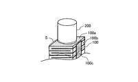
- one conventional electronic device includes a laminated piezoelectric element (element) 100 and a driven element (member other than the element 100) 200 driven by the element 100.
- the driven element 200 is bonded to the upper surface 100a of the element 100 using an adhesive S (see, for example, Patent Document 1).
- piezoelectric is used as a term representing a concept including “piezoelectric” and “electrostriction”. . Therefore, in this specification and the like, for example, a piezoelectric element includes both “an element having a piezoelectric effect (piezoelectric element) and an element having an electrostrictive effect (electrostrictive element)”.
- an epoxy resin adhesive is generally used as the adhesive S.
- the epoxy resin-based adhesive oozes out from a portion where a part of “resin and additive” is applied after coating. This phenomenon is called “epoxy bleed out”. Accordingly, as shown in FIG. 13, even when the epoxy resin adhesive S is applied only to the upper surface 100a, a part of the component of the adhesive S penetrates the side surface 100b of the element 100 by epoxy bleeding out. put out. At this time, if the electrode (outer surface electrode) 100c is provided on the side surface 100b of the element 100, a part of the component of the adhesive S that bleeds out from the adhesive S covers the electrode 100c.
- the electrode 100c is “an electrode for connecting the element 100 and an external circuit”
- the solderable area of the electrode 100c is reduced, and therefore the solder strength is reduced, or the external circuit
- the connection with is insufficient.
- the electrode 100c provided in the side surface 100b may react with a part of component of the adhesive S bleed out from the adhesive S, and may change in quality.
- One of the objects of the present invention is to provide an electronic device that can eliminate adverse effects of epoxy bleed-out on an electrode (outer surface electrode) disposed on the outer surface of the element.
- An electronic device according to the present invention (hereinafter also referred to as “this device”) is bonded to an element having an outer surface electrode disposed on a part of the outer surface, and an epoxy resin adhesive to the element. And a member.
- the element include a piezoelectric element and a semiconductor chip.
- the member to be bonded may be a driven element driven by an element or a substrate for fixing the element.
- the adhesive is disposed on a portion of the outer surface of the element other than the portion where the outer surface electrode is present. That is, the member is bonded to a place other than the portion where the outer surface electrode is present. Furthermore, this apparatus includes a weir portion made of a material that prevents epoxy bleed out of the adhesive between the adhesive and the outer surface electrode.
- the weir portion is disposed between the adhesive and the outer surface electrode. Therefore, even if epoxy bleed-out occurs, a part of the adhesive does not reach the outer surface electrode. As a result, the above-described problem is solved.
- the material constituting the weir is preferably a material mainly composed of a novolac type epoxy resin.
- the novolac type epoxy resin includes a phenol novolac type epoxy resin and a cresol novolac type epoxy resin.
- a novolac type epoxy resin is widely known as a semiconductor sealing resin.
- the present inventor has obtained knowledge that “a novolac type epoxy resin can effectively suppress epoxy bleed-out of an epoxy resin adhesive”. Furthermore, the present inventor has obtained the knowledge that “the novolac type epoxy resin itself hardly spreads by epoxy bleed out”. Therefore, the novolac type epoxy resin is suitable as a material constituting the dam portion.
- the element is an element provided with a piezoelectric body including a piezoelectric layer and a first electrode layer and a second electrode layer facing each other with the piezoelectric layer interposed therebetween,
- the outer surface electrode includes a first electrode that is “an electrode constituted by an end of the first electrode layer or an electrode layer connected to an end of the first electrode layer”, and “the second electrode An electrode constituted by an end portion of the layer, or a second electrode which is an “electrode layer connected to an end portion of the second electrode layer”.
- the piezoelectric element has a characteristic that an electric charge is generated on the surface when a sudden temperature change is applied. This phenomenon is also called the pyroelectric effect.
- the electric charge generated on the surface of the piezoelectric element generates an electric field in a direction opposite to the polarization direction of the piezoelectric element, thereby unpolarizing the piezoelectric element (this phenomenon is also referred to as “depolarization” or “depolarization”). ).
- depolarization this phenomenon is also referred to as “depolarization” or “depolarization”.
- the amount of mechanical displacement of the piezoelectric element with respect to the voltage applied to the piezoelectric element decreases. That is, the characteristic deterioration of the piezoelectric element occurs.
- the dam portion has a semiconductivity by adding a conductive material to the material constituting the dam portion, and straddles the first electrode and the second electrode (that is, the first electrode). And the second electrode).
- a conductive material carbon, Ag, Au, Cu, or an alloy thereof may be used. Alternatively, it is preferable to use carbon that can be easily adjusted to a desired resistivity for the conductive material.
- the first electrode and the second electrode are connected by the semiconductive weir portion, the first electrode layer and the second electrode layer are connected by a conductor having a relatively large resistance value. Is done.
- the generation of the pyroelectric effect can be suppressed. That is, only by providing the dam part, the problem caused by the epoxy bleed out of the adhesive and the problem caused by the pyroelectric effect (occurrence of depolarization) can be solved simultaneously.
- the element is a polyhedral laminated piezoelectric element formed by laminating a plurality of the piezoelectric bodies. Two or more ends of the plurality of first electrode layers included in the element are exposed on one side surface of the polyhedron. Two or more ends of the plurality of second electrode layers included in the element are exposed on the one side surface.
- the first electrode is an electrode layer that connects ends of the two or more first electrode layers exposed on the one side surface on the one side surface.
- the second electrode is an electrode layer that connects ends of the two or more second electrode layers exposed on the one side surface on the one side surface.
- FIG. 1 is a schematic perspective view of an electronic device (first device) according to the first embodiment of the present invention.
- 2A is a left side view of the multilayer piezoelectric element shown in FIG. 1
- FIG. 2B is a front view of the multilayer piezoelectric element shown in FIG. 1
- FIG. 3 is a right side view of the multilayer piezoelectric element shown in FIG.
- FIG. 3 is a schematic perspective view of an electronic device (second device) according to the second embodiment of the present invention.
- 4 is a front view of various internal electrode layers used in the second device shown in FIG.
- FIG. 5 is a right side view of the piezoelectric element shown in FIG. 6 is a rear view of the piezoelectric element shown in FIG. FIG.
- FIG. 7 is a right side view of the piezoelectric element shown in FIG. 8 is a left side view of the piezoelectric element shown in FIG.
- FIG. 9 is a back view of the piezoelectric element shown in FIG.
- FIG. 10 is a right side view of the piezoelectric element shown in FIG.
- FIG. 11 is a left side view of the piezoelectric element shown in FIG.
- FIG. 12 is a schematic view of a modification of the present invention.
- FIG. 13 is a schematic perspective view of an electronic device to which the present invention is not applied.
- an electronic device (hereinafter also referred to as “first device”) 10 according to the first embodiment of the present invention includes a laminated piezoelectric element (piezoelectric element) 20 and a driven element 30. And comprising.
- the driven element 30 is, for example, a rod or a weight that is slid or vibrated by expansion and contraction of the piezoelectric element 20.
- the piezoelectric element 20 includes a plurality of piezoelectric layers (layers made of a piezoelectric material) 21, a plurality of first internal electrode layers 22, a plurality of second internal electrode layers 23, and a first side surface.
- An electrode 24, a second side electrode 25, a first end piezoelectric layer 26, a second end piezoelectric layer 27, a dam (upper dam) 28 and a dam (lower dam) 29 are provided.
- the piezoelectric element 20 has a rectangular parallelepiped shape having sides along the X axis, the Y axis, and the Z axis that are orthogonal to each other.
- the length of the piezoelectric element 20 in the X-axis direction is 1 mm
- the length of the piezoelectric element 20 in the Y-axis direction is 1 mm
- the length (height) of the piezoelectric element 20 in the Z-axis direction is 2 mm.
- the main component of the piezoelectric layer 21 is a piezoelectric material (for example, lead zirconate titanate, PZT).
- the thickness (length in the Z-axis direction) of each piezoelectric layer 21 is, for example, 0.019 mm.
- the piezoelectric layer 21 is a fired body.
- the piezoelectric layer 21 is subjected to polarization processing along the Z-axis direction.
- the shape of the piezoelectric layer 21 in plan view is a square having a side length of 1 mm. That is, the planar shape of the piezoelectric layer 21 is a square having sides along the X axis and the Y axis.
- the material of the first internal electrode layer 22 is a conductive material (eg, Ag—Pd alloy, Ag, etc.).
- the thickness of the first internal electrode layer 22 is, for example, 0.001 mm.
- Both ends of the first internal electrode layer 22 in the Y-axis direction extend to both ends of the piezoelectric layer 21 in the Y-axis direction.
- the X-axis positive direction end of the first internal electrode layer 22 extends to the X-axis positive direction end of the piezoelectric layer 21.
- the X-axis negative direction end of the first internal electrode layer 22 extends to the vicinity of the X-axis negative direction end of the piezoelectric layer 21, but reaches the X-axis negative direction end of the piezoelectric layer 21. Absent.
- the material of the second internal electrode layer 23 is the same conductive material as that of the first internal electrode layer 22 (for example, Ag—Pd alloy and Ag).
- the thickness of the second internal electrode layer 23 is the same as the thickness of the first internal electrode layer 22.
- Both ends of the second internal electrode layer 23 in the Y-axis direction extend to both ends of the piezoelectric layer 21 in the Y-axis direction.
- the X-axis negative direction end of the second internal electrode layer 23 extends to the X-axis negative direction end of the piezoelectric layer 21.
- the X-axis positive direction end of the second internal electrode layer 23 extends to the vicinity of the X-axis positive direction end of the piezoelectric layer 21, but reaches the X-axis positive direction end of the piezoelectric layer 21. Absent.
- the second internal electrode layer 23 is disposed so as to face the first internal electrode layer 22 with the piezoelectric layer 21 interposed therebetween. That is, the first internal electrode layer 22 and the second internal electrode layer 23 are provided so as to face each other with the piezoelectric layer 21 interposed therebetween.
- the piezoelectric layer 21 sandwiched between the first internal electrode layer 22 and the second internal electrode layer 23 is stacked in the Z-axis direction (stacking direction, direction orthogonal to the layer surface of each layer).
- the first internal electrode layers 22 and the second internal electrode layers 23 are alternately stacked with the piezoelectric layers 21 interposed therebetween.
- the number of stacked piezoelectric layers 21 is not limited, but is 90 layers, for example. However, in FIGS. 1 to 3 and the like, twelve piezoelectric layers 21 are laminated in order to simplify the drawings.
- the first side surface electrode 24 is an electrode layer formed on the right side surface of the piezoelectric element 20 (the surface at the end in the positive direction of the X axis and parallel to the YZ plane).
- the material of the first side electrode 24 is the same conductive material as the first internal electrode layer 22 (for example, Ag—Pd alloy, Ag, etc.).
- the shape of the first side electrode 24 in a front view is a rectangle having a longitudinal direction in the height direction (Z-axis direction) of the piezoelectric element 20.
- the first side electrode 24 electrically connects all of the plurality of first internal electrode layers 22.
- a conductive wire (not shown) connected to an external drive circuit is soldered to the first side electrode 24.
- the second side electrode 25 is an electrode layer formed on the left side surface of the piezoelectric element 20 (the surface at the end in the negative direction of the X axis and parallel to the YZ plane).
- the material of the second side electrode 25 is the same conductive material as the first internal electrode layer 22 (for example, Ag—Pd alloy, Ag, etc.).
- the shape of the second side electrode 25 in a front view is a rectangle having a longitudinal direction in the height direction (Z-axis direction) of the piezoelectric element 20.
- the second side electrode 25 electrically connects all of the plurality of second internal electrode layers 23.
- a conductive wire (not shown) connected to an external drive circuit is soldered to the second side electrode 25.
- the first end piezoelectric layer 26 is laminated on the top of the piezoelectric layer 21 (and the first internal electrode layer 22 located on the top) of the plurality of piezoelectric layers 21.
- the first end piezoelectric layer 26 is also referred to as the upper end piezoelectric layer 26.
- the main component of the first end piezoelectric layer 26 is the same as the main component of the piezoelectric layer 21.
- the first end piezoelectric layer 26 is a fired body.
- the upper surface 20a of the first end piezoelectric layer 26 is exposed. As will be described later, an adhesive S is applied to the upper surface 20a, and the driven element 30 is bonded to a substantially central portion of the upper surface 20a.
- the second end piezoelectric layer 27 is laminated below the piezoelectric layer 21 located at the bottom of the plurality of piezoelectric layers 21 (and the first internal electrode layer 22 located at the bottom).
- the second end piezoelectric layer 27 is also referred to as a lower end piezoelectric layer 27.
- the main component of the second end piezoelectric layer 27 is the same as the main component of the piezoelectric layer 21.
- the second end piezoelectric layer 27 is a fired body.
- the lower surface 20b of the second end piezoelectric layer 27 is exposed.
- the lower surface 20b may be bonded to a member such as a substrate with an adhesive S. In this case, the adhesive S is applied only to the lower surface of the piezoelectric element 20.
- a portion sandwiched between “first internal electrode layer 22 and second internal electrode layer 23” adjacent to each other and facing each other is an active portion.
- the active portion is applied with an electric field that changes when a “changing voltage (potential difference)” is applied between the first internal electrode layer 22 and the second internal electrode layer 23, and is thereby displaced (particularly, Part extending and contracting in the Z-axis (height) direction.
- the weir part (upper weir part) 28 is made of a material mainly composed of a novolac type epoxy resin.
- the weir portion 28 is provided in a band shape at the upper end portion (Z-axis positive direction end portion) of the piezoelectric element 20. That is, the dam portion 28 is a right side surface, a front surface, a left side surface, and a back surface of the piezoelectric element 20 (which is a surface parallel to the Z axis, that is, a direction orthogonal to the stacking direction, and is hereinafter also referred to as “vertical wall surface”). Is formed so as to have a predetermined width (substantially constant width) W1 from the upper end side of the piezoelectric element 20 (side forming the boundary between the upper surface 20a and the vertical wall surface).
- the dam portion 28 is provided on the right side surface of the piezoelectric element 20 so as to have the predetermined width W1 between the upper end and the upper end side of the first side electrode 24 (FIG. 2). (See (C).)
- the dam portion 28 is provided on the front surface of the piezoelectric element 20 so as to have the predetermined width W1 from the upper end side (see FIG. 2B).
- the dam portion 28 is provided on the left side surface of the piezoelectric element 20 so as to have the predetermined width W1 between the upper end and the upper end side of the second side electrode 25 (see FIG. 2A).
- the dam portion 28 is provided on the back surface of the piezoelectric element 20 so as to have the predetermined width W1 from the upper end side.
- the dam portion (lower dam portion) 29 is provided in a band shape at the lower end portion (Z-axis negative direction end portion) of the piezoelectric element 20. That is, the dam portion 29 has a predetermined width (substantially constant width) W2 on the surface of the vertical wall surface of the piezoelectric element 20 from the lower end side (side that forms the boundary between the lower surface 20b and the vertical wall surface) of the piezoelectric element 20. So that it is formed.
- the dam portion 29 is provided on the right side surface of the piezoelectric element 20 so as to have the predetermined width W2 between the lower end and the lower end side of the first side electrode 24 (FIG. 2). (See (C).)
- the dam portion 28 is provided on the front surface of the piezoelectric element 20 so as to have the predetermined width W2 from the lower end side (see FIG. 2B).
- the dam portion 28 is provided on the left side surface of the piezoelectric element 20 so as to have the predetermined width W2 between the lower end and the lower end side of the second side electrode 25 (see FIG. 2A).
- the dam portion 28 is provided on the back surface of the piezoelectric element 20 so as to have the predetermined width W2 from the lower end side.
- the driven element 30 has a cylindrical shape. Therefore, the lower surface of the driven element 30 is flat.
- the driven element 30 is bonded to the piezoelectric element 20 by bonding the lower surface of the driven element 30 to the central portion of the upper surface 20 a of the piezoelectric element 20 with an adhesive S.
- the shape of the driven element 30 may be other than a cylindrical shape.
- the driven element 30 is made of, for example, a material mainly containing any one of “carbon, heavy metal, heavy metal carbide, heavy metal boride, and heavy metal nitride”.
- the heavy metal herein, tungsten and tantalum are particularly preferable, and tungsten carbide (WC), tungsten boride (WB), tantalum nitride (TaN), and the like are preferably used.
- the adhesive S is applied only to the upper surface 20a (and the lower surface 20b) in the manufacturing process.
- the adhesive S is an epoxy adhesive.
- an adhesive having a “tensile shear strength” of 15 N / mm 2 or more measured based on a method in accordance with “JIS K6850” is preferably used.
- the viscosity of the adhesive S before curing is preferably 50 to 200 Pa ⁇ s.
- the end portions of the plurality of first internal electrode layers 22, the end portions of the plurality of second internal electrode layers 23, the first side surface electrode 24, and the second side surface electrode 25 are included in the piezoelectric element 20. It is arranged on the surface (outer surface). That is, these electrodes and the end portions of the electrodes have outer surface electrodes arranged on a part of the outer surface of the piezoelectric element 20.
- the driven element 30 constitutes a member that is bonded to the piezoelectric element 20 using an epoxy resin adhesive S.
- the adhesive S is disposed on the outer surface of the piezoelectric element 20 other than the portion where the “outer surface electrode” exists (in this example, the upper surface 20a and the lower surface 20b).
- the electronic device 10 is manufactured by a known method. Hereinafter, a method for manufacturing the electronic device 10 will be briefly described.
- First step “piezoelectric tape molding) First, “a plurality of piezoelectric tapes (first piezoelectric tapes that are ceramic green sheets)” and “a first end piezoelectric layer and a second end piezoelectric layer” that form the piezoelectric layer 21 by the doctor blade method. “A plurality of piezoelectric tapes (second piezoelectric tapes which are ceramic green sheets)” are prepared.
- Second step (internal electrode layer printing) Next, a conductor layer having a predetermined pattern is formed on each of the first piezoelectric tapes by screen printing. This conductor layer is a layer that becomes the first internal electrode layer 22 and the second internal electrode layer 23 after firing.
- Third step (adhesive layer printing) An adhesive paste is printed on each piezoelectric tape by screen printing. 4).
- a material having a novolac epoxy resin as a main component is applied to the upper ends of the vertical wall surfaces (right side surface, left side surface, front surface, and back surface) of the piezoelectric element 20 by a certain width W1, and is cured by heating.
- a material mainly composed of a novolac type epoxy resin is applied to the lower end of the vertical wall surface of the piezoelectric element 20 by a certain width W2, and is cured by heating.
- the adhesive S is applied to the upper surface 20a of the piezoelectric element 20, and the piezoelectric element 20 and the driven element 30 are bonded. Further, if necessary, an adhesive S is applied to the lower surface 20b to bond the piezoelectric element 20 and another member such as a substrate. Thus, the electronic device 10 is manufactured.
- the piezoelectric element 20 includes the dam portion 28 (and the dam portion 29) mainly composed of a novolac type epoxy resin.
- the novolac type epoxy resin includes a phenol novolac type epoxy resin and a cresol novolac type epoxy resin.
- a novolac type epoxy resin is widely known as a semiconductor sealing resin. The present inventor has obtained knowledge that “a novolac type epoxy resin can effectively suppress epoxy bleed-out of an epoxy resin adhesive”. Furthermore, the present inventor has obtained the knowledge that “the novolac type epoxy resin itself hardly spreads by epoxy bleed out”.
- a part of the adhesive S is constituted by the outer surface electrodes (for example, the first side electrode 24, the second side electrode 25, and the end portion of the first internal electrode layer 22 exposed on the front surface or the back surface of the piezoelectric element 20).
- the electrode and the electrode constituted by the end portion of the second internal electrode layer 23 exposed on the front surface or the back surface of the piezoelectric element 20 do not reach.
- the piezoelectric element 20 having high connection reliability with an external circuit is provided. Furthermore, the material of the outer surface electrode can be selected without considering the reaction with “a part of the components of the adhesive S” that exudes from the adhesive S by epoxy bleeding out.
- the dam portion (lower dam portion) 29 may not be provided.
- the front surface and the back surface of the piezoelectric element 20 may be covered with a protective film (not shown).
- the weir portion 28 (and the weir portion 29) may not be provided on the front surface and the back surface.
- the dam portion 28 and the dam portion 29 do not have to have a constant width.
- the dam portion 28 and the dam portion 29 are preferably formed at least “so as to cross a straight line connecting the portion to which the adhesive S is applied and the outer surface electrode along the outer surface of the piezoelectric element 20”. .
- the electronic device (hereinafter also referred to as “second device”) 40 includes a piezoelectric element (laminated piezoelectric element) 50 and a driven element 30. And comprising.
- the driven element 30 is the same member as the driven element 30 included in the first device 10.
- the piezoelectric element 50 has a rectangular parallelepiped shape similar to that of the piezoelectric element 20.
- the relationship between each surface (outer surface) of the piezoelectric element 50 and the coordinate axis is as follows.
- Front A surface of the end of the piezoelectric element 50 in the negative direction of the X axis and parallel to the YZ plane.
- Back surface the surface of the piezoelectric element 50 at the end in the positive direction of the X axis and parallel to the YZ plane.
- Right side surface the surface of the Y-axis negative direction end portion of the piezoelectric element 50 and parallel to the XZ plane.
- Left side surface the surface of the piezoelectric element 50 at the end in the positive Y-axis direction and parallel to the XZ plane.
- Upper surface the surface of the piezoelectric element 50 at the end in the positive direction of the Z-axis and parallel to the XY plane.
- Lower surface the surface of the piezoelectric element 50 at the end in the negative Z-axis direction and parallel to the XY plane.
- the piezoelectric element 50 includes the following types of “layers (or films)”.
- Piezoelectric layer active piezoelectric layer 51a, upper inactive piezoelectric layer 51b, lower inactive piezoelectric layer 51c.
- First internal electrode layer type A1 electrode layer 52a1, type A2 electrode layer 52a2.
- Second internal electrode layer Type B1 electrode layer 53b1, Type B2 electrode layer 53b2.
- Right side electrode right side main electrode layer 54a, right side sub electrode layer 54b.
- Left side electrode left side main electrode layer 55a, left side sub electrode layer 55b.
- Protective film front protective film 56a, back protective film 56b.
- Right side dam part right side upper dam part 57a, right side lower dam part 57b.
- Left side dam part left side upper dam part 58a, left side lower dam part 58b.
- the piezoelectric layer includes an active piezoelectric layer 51a, an upper inactive piezoelectric layer 51b, and a lower inactive piezoelectric layer 51c.
- the active piezoelectric layer 51 a is a layer similar to the piezoelectric layer 21 of the piezoelectric element 20.
- the piezoelectric element 50 includes a plurality of active piezoelectric layers 51a.
- the upper inert piezoelectric layer 51 b is a layer similar to the first end piezoelectric layer 26 of the piezoelectric element 20.
- the lower inert piezoelectric layer 51 c is a layer similar to the second end piezoelectric layer 27 of the piezoelectric element 20.
- the material of the first internal electrode layer and the second internal electrode layer is the same as the material of the first internal electrode layer 22.
- the first internal electrode layer includes a plurality of “type A1 electrode layers 52a1” and a plurality of “type A2 electrode layers 52a2”. That is, the piezoelectric element 50 includes a plurality of “type A1 electrode layers 52a1” and a plurality of “type A2 electrode layers 52a2”.
- the second internal electrode layer includes a plurality of “type B1 electrode layers 53b1” and a plurality of “type B2 electrode layers 53b2”. That is, the piezoelectric element 50 includes a plurality of “type B1 electrode layers 53b1” and a plurality of “type B2 electrode layers 53b2”.
- the first internal electrode layer (any of type A1 electrode layer 52a1 and type A2 electrode layer 52a2) is composed of a second internal electrode layer (any of type B1 electrode layer 53b1 and type B2 electrode layer 53b2) and an active piezoelectric layer. It arrange
- FIG. 4 is a diagram showing the shapes of these electrode layers.
- the white portions are the active piezoelectric layers 51a existing below the respective electrode layers.
- the type A1 electrode layer 52a1 is an electrode layer having the planar shape shown in FIG.
- the end in the Y-axis negative direction of the type A1 electrode layer 52a1 reaches only the vicinity of the center in the X-axis direction of the end in the Y-axis negative direction of the active piezoelectric layer 51a.
- the Y-axis positive direction end of the type A1 electrode layer 52a1 reaches only the vicinity of both ends in the X-axis direction of the Y-axis positive direction end of the active piezoelectric layer 51a.
- Both end portions in the X-axis direction of the type A1 electrode layer 52a1 reach portions other than the vicinity of the Y-axis negative direction end portions at both ends in the X-axis direction of the active piezoelectric layer 51a.
- the type A2 electrode layer 52a2 is an electrode layer having the planar shape shown in FIG.
- the Y-axis negative direction end portion of the type A2 electrode layer 52a2 reaches only the vicinity of the central portion in the X-axis direction of the Y-axis negative direction end portion of the active piezoelectric layer 51a.
- the Y-axis positive direction end portion of the type A2 electrode layer 52a2 reaches a portion that is a predetermined distance away from the Y-axis positive direction end portion of the active piezoelectric layer 51a.
- Both ends of the type A2 electrode layer 52a2 in the X-axis direction reach portions other than the vicinity of both ends in the Y-axis direction of both ends of the active piezoelectric layer 51a in the X-axis direction.
- the type B1 electrode layer 53b1 is an electrode layer having a planar shape shown in FIG.
- the Y-axis positive direction end portion of the type B1 electrode layer 53b1 reaches only the vicinity of the central portion in the X-axis direction of the Y-axis positive direction end portion of the active piezoelectric layer 51a.
- the end in the Y-axis negative direction of the type B1 electrode layer 53b1 reaches only the vicinity of both ends in the X-axis direction of the end in the Y-axis negative direction of the active piezoelectric layer 51a.
- Both ends of the type B1 electrode layer 53b1 in the X-axis direction reach portions other than the vicinity of the ends in the Y-axis positive direction of both ends of the active piezoelectric layer 51a in the X-axis direction. That is, the type B1 electrode layer 53b1 has a shape obtained by rotating the type A1 electrode layer 52a1 by 180 degrees around the Z axis.
- the type B2 electrode layer 53b2 is an electrode layer having the planar shape shown in FIG.
- the Y-axis positive direction end portion of the type B2 electrode layer 53b2 reaches only the vicinity of the central portion in the X-axis direction of the Y-axis positive direction end portion of the active piezoelectric layer 51a.
- the Y-axis negative direction end portion of the type B2 electrode layer 53b2 reaches a portion that is a predetermined distance away from the Y-axis negative direction end portion of the active piezoelectric layer 51a.
- Both ends of the type B2 electrode layer 53b2 in the X-axis direction reach portions other than the vicinity of both ends in the Y-axis direction of both ends of the active piezoelectric layer 51a in the X-axis direction. That is, the type B2 electrode layer 53b2 has a shape obtained by rotating the type A2 electrode layer 52a2 by 180 degrees around the Z axis.
- the piezoelectric element 50 is formed by laminating a plurality of active piezoelectric layers 51a on a lower inactive piezoelectric layer 51c, and further on the uppermost active piezoelectric layer 51a of the laminated body.
- the upper inert piezoelectric layer 51b is laminated on the substrate.
- the piezoelectric element 50 is a stacked piezoelectric element in which an active piezoelectric layer sandwiched between a first internal electrode layer and a second internal electrode layer is stacked.
- the first internal electrode layer (type A1 electrode layer 52a1 and type A2 electrode layer 52a2) and the second internal electrode layer (type B1 electrode layer 53b1 and type B2 electrode layer 53b2) are arranged in the order shown in FIGS.
- A1 indicates that the type A1 electrode layer 52a1 is formed.
- A2 indicates that the type A2 electrode layer 52a2 is formed
- B1 indicates that the type B1 electrode layer 53b1 is formed
- B2 indicates that the type B2 electrode layer 53b2 is formed.
- the right side electrode includes one right side main electrode layer 54a and four right side sub electrode layers 54b.
- the right side main electrode layer 54 a and the right side sub electrode layer 54 b are formed on the right side of the piezoelectric element 50.
- the right side main electrode layer 54a has a cross shape when viewed from the front. More specifically, both end portions in the X-axis direction of the central portion in the Z-axis direction of the right side main electrode layer 54a reach both end portions in the X-axis direction of the piezoelectric element 50. Both ends in the Z-axis direction of the center portion in the X-axis direction of the right side main electrode layer 54a reach portions that are separated from the both ends in the Z-axis direction of the piezoelectric element 50 by a predetermined distance. The edge has not been reached.
- the right side main electrode layer 54a is formed so as to cover the end portion of the first internal electrode layer 52 (type A1 electrode layer 52a1 and type A2 electrode layer 52a2) exposed on the right side surface of the piezoelectric element 50. Thereby, the right side main electrode layer 54a connects the plurality of first internal electrode layers to each other on the “right side which is one side surface of the piezoelectric element 50”.
- the right side sub-electrode layer 54b has a rectangular shape when viewed from the front. More specifically, the right side sub-electrode layer 54 b is disposed at the four corners on the right side of the piezoelectric element 50. In other words, the right side sub-electrode layer 54b is disposed in a portion of the right side of the piezoelectric element 50 that is not covered by the right side main electrode layer 54a.
- the right side sub-electrode layer 54 b covers “the end portions of the plurality of second internal electrode layers (actually the type B1 electrode layer 53 b 1)” exposed on the right side surface of the piezoelectric element 50.
- the right side sub-electrode layer 54 b connects the plurality of second internal electrode layers exposed on the right side of the piezoelectric element 50.
- each right side sub-electrode layer 54b is separated from the right side main electrode layer 54a by a small distance and is not connected to the right side main electrode layer 54a.
- the left side electrode includes one left side main electrode layer 55a and four left side sub electrode layers 55b.
- the left side main electrode layer 55 a and the left side sub electrode layer 55 b are formed on the left side of the piezoelectric element 50.
- the left side main electrode layer 55a has a cross shape when viewed from the front. More specifically, both ends in the X-axis direction of the central portion in the Z-axis direction of the left side main electrode layer 55a reach both ends in the X-axis direction of the piezoelectric element 50. Both end portions in the Z-axis direction of the central portion in the X-axis direction of the left side main electrode layer 55a reach portions that are separated from the both end portions in the Z-axis direction of the piezoelectric element 50 by a predetermined distance. The edge has not been reached.
- the left side main electrode layer 55a is formed so as to cover the ends of the second internal electrode layers (type B1 electrode layer 53b1 and type B2 electrode layer 53b2) exposed on the right side surface of the piezoelectric element 50. Thereby, the left side main electrode layer 55a connects the plurality of second internal electrode layers at “the left side which is one side surface of the piezoelectric element 50”.
- the left side sub-electrode layer 55b has a rectangular shape when viewed from the front. More specifically, the left side sub-electrode layer 55 b is arranged at the four corners on the left side of the piezoelectric element 50. In other words, the left side sub-electrode layer 55b is disposed in a portion of the left side of the piezoelectric element 50 that is not covered by the left side main electrode layer 55a.
- the left side sub-electrode layer 55 b covers “the end portions of the plurality of first internal electrode layers (actually, the type A1 electrode layer 52 a 1)” exposed on the left side surface of the piezoelectric element 50.
- the left side sub-electrode layer 55 b connects the plurality of first internal electrode layers exposed on the left side of the piezoelectric element 50. However, each left side sub-electrode layer 55b is separated from the left side main electrode layer 55a by a small distance and is not connected to the left side main electrode layer 55a.
- the protective film is made of, for example, an epoxy resin.
- the protective film includes a front protective film 56a provided on the front surface of the piezoelectric element 50 and a back protective film 56b provided on the back surface of the piezoelectric element.
- the front protective film 56a and the back protective film 56b have the same shape.
- both ends in the Y-axis direction of the back surface protective film 56 b reach both ends in the Y-axis direction of the piezoelectric element 50.
- Each of both end portions in the Z-axis direction of the back surface protective film 56b reaches a portion separated from each of both end portions in the Z-axis direction of the piezoelectric element 50 by a predetermined distance. That is, the Z-axis positive direction end portion of the back surface protective film 56 b does not reach the upper end side of the piezoelectric element 50.
- the Z-axis negative direction end portion of the back surface protective film 56 b does not reach the lower end side of the piezoelectric element 50.
- the back surface protective film 56 b completely covers the ends of the “first internal electrode layer and second internal electrode layer” exposed on the back surface of the piezoelectric element 50.
- the front protective film 56 a completely covers the ends of the “first internal electrode layer and second internal electrode layer” exposed on the front surface of the piezoelectric element 50.
- the right side weir and the left side weir are made of a material mainly composed of a novolac type epoxy resin.
- a conductive material is added to the material (the material constituting the dam portion), whereby the right side dam portion and the left side dam portion are semiconductive.
- the conductive material to be added carbon, Ag, Au, Cu, or an alloy thereof is used. In particular, it is preferable to use carbon that can be easily adjusted to a desired resistivity.
- the resistance of the semiconductive film is much smaller than the resistance of the insulating film and much larger than the resistance of the conductor film.
- the right side weir part includes a right side upper weir part 57a and a right side lower weir part 57b.
- the right side upper dam part 57a and the right side lower dam part 57b are formed at the upper part and the lower part of the right side face of the piezoelectric element 50, respectively.
- the right side upper dam part 57a and the right side lower dam part 57b have substantially the same rectangular shape in plan view.
- both ends in the X-axis direction of the upper side weir portion 57a on the right side surface reach both ends in the X-axis direction of the piezoelectric element 50.
- the Z-axis positive direction end (upper end) of the right side upper surface weir portion 57a is “the upper electrode side of the piezoelectric element 50 and the internal electrode layer exposed at a position closest to the upper end side on the right side surface of the piezoelectric element 50. The position has reached “a position between the type B1 electrode layer 53b1”. However, the upper end of the upper right side weir portion 57 a does not reach the upper end side of the piezoelectric element 50.
- the upper right weir 57a on the right side surface covers the type B1 electrode layer 53b1 exposed at a position closest to the upper end side on the right side surface of the piezoelectric element 50.
- the Z-axis negative direction end portion (lower end) of the right side upper surface weir portion 57a reaches a portion slightly separated in the Z-axis positive direction from the Z-axis direction central portion of the piezoelectric element 50.
- the right side upper weir portion 57a connects the “right side main electrode layer 54a and the pair of right side sub electrode layers 54b” existing at the upper part of the right side.
- the right side upper dam portion 57a is formed so as to straddle the right side main electrode layer 54a and the pair of right side sub electrode layers 54b.
- the first internal electrode layer and the second internal electrode layer are connected through the semiconductive film (the right side upper surface weir portion 57a).
- the X axis direction both ends of the right side lower dam portion 57b reach the X axis direction both ends of the piezoelectric element 50.
- the Z-axis positive direction end (upper end) of the right side lower dam portion 57b reaches a portion slightly away from the Z-axis direction central portion of the piezoelectric element 50 in the Z-axis negative direction.
- the Z-axis negative direction end portion (lower end) of the right side lower weir portion 57b is “an internal electrode layer exposed at a position closest to the lower end side of the lower side of the piezoelectric element 50 and the right side surface of the piezoelectric element 50. The position has reached “a position between the type B1 electrode layer 53b1”.
- the lower end of the upper right side weir portion 57 a does not reach the lower end side of the piezoelectric element 50. That is, the lower right dam portion 57b on the right side surface covers the type B1 electrode layer 53b1 exposed at the position closest to the lower end side on the right side surface of the piezoelectric element 50.
- the right-side lower weir portion 57b connects the “right-side main electrode layer 54a and the pair of right-side sub-electrode layers 54b” existing at the lower part of the right-side surface.
- the right side lower dam portion 57b is formed so as to straddle the right side main electrode layer 54a and the pair of right side sub electrode layers 54b.
- the first internal electrode layer and the second internal electrode layer are connected through a semiconductive film (right side lower dam portion 57b).
- the right side upper dam part 57a and the right side lower dam part 57b are arranged so as to be separated from each other by a predetermined distance in the vicinity of the center part in the Z-axis direction of the right side surface of the piezoelectric element 50. Accordingly, the right side main electrode layer 54a is exposed in the vicinity of the central portion of the right side surface of the piezoelectric element 50 in the Z-axis direction. External wiring (not shown) is soldered to the exposed portion of the right side main electrode layer 54a.
- a right side upper weir portion 57a extends between the exposed portion of the right side main electrode layer 54a and the upper surface 50a of the piezoelectric element 50. Therefore, even when the epoxy resin adhesive S is applied to the upper surface 50a, the epoxy bleed-out of the adhesive S is blocked by the right upper surface weir portion 57a. As a result, it is avoided that a part of the component of the adhesive S reaches the exposed portion of the right side main electrode layer 54a, so that the external wiring is firmly soldered to the exposed portion of the right side main electrode layer 54a. It can be carried out.
- the left side dam portion includes a left side upper dam portion 58a and a left side lower dam portion 58b.
- the left side upper dam portion 58a and the left side lower dam portion 58b are formed at the upper and lower portions of the left side surface of the piezoelectric element 50, respectively.
- the left side upper dam part 58a and the left side lower dam part 58b have substantially the same rectangular shape in plan view.
- both end portions in the X-axis direction of the left side upper weir portion 58a reach both end portions in the X-axis direction of the piezoelectric element 50.
- the Z-axis positive direction end (upper end) of the left side upper weir 58a is “an internal electrode layer exposed at a position closest to the upper end on the upper end side of the piezoelectric element 50 and the left side surface of the piezoelectric element 50. The position has reached “a position between the type B1 electrode layer 53b1”. However, the upper end of the upper left side weir 58 a does not reach the upper end side of the piezoelectric element 50.
- the left side upper dam portion 58a covers the type B1 electrode layer 53b1 exposed at a position closest to the upper end side on the left side surface of the piezoelectric element 50.
- the Z-axis negative direction end (lower end) of the left side upper dam portion 58a reaches a portion slightly separated in the Z-axis positive direction from the Z-axis direction central portion of the piezoelectric element 50.
- the left side upper weir portion 58a connects the “left side main electrode layer 55a and the pair of left side sub electrode layers 55b” existing at the upper part of the left side.
- the left side upper dam portion 58a is formed so as to straddle the left side main electrode layer 55a and the pair of left side sub electrode layers 55b.
- the first internal electrode layer and the second internal electrode layer are connected through the semiconductive film (left side upper weir portion 58a).
- the X axis direction both ends of the left side lower dam portion 58b reach the X axis direction both ends of the piezoelectric element 50.
- the Z-axis positive direction end (upper end) of the left side lower dam portion 58b reaches a portion slightly away from the Z-axis direction central portion of the piezoelectric element 50 in the Z-axis negative direction.
- the Z-axis negative direction end (lower end) of the left side lower dam portion 58b is “an internal electrode layer exposed at a position closest to the lower end side on the left side surface of the piezoelectric element 50 and the left side surface of the piezoelectric element 50. The position has reached “a position between the type B1 electrode layer 53b1”.
- the lower end of the left side lower dam portion 58 b does not reach the lower end side of the piezoelectric element 50. That is, the left side lower dam portion 58b covers the type B1 electrode layer 53b1 exposed at a position closest to the lower end side on the left side surface of the piezoelectric element 50.
- the left side lower dam portion 58b connects the “left side main electrode layer 55a and the pair of left side sub electrode layers 55b” existing at the lower part of the left side surface, similarly to the right side lower dam portion 57b.
- the first internal electrode layer and the second internal electrode layer are connected through the semiconductive film (the left side lower dam portion 58b).
- the left side upper dam portion 58a and the left side lower dam portion 58b are arranged so as to be separated from each other by a predetermined distance in the vicinity of the central portion of the left side surface of the piezoelectric element 50 in the Z-axis direction. Accordingly, the left side main electrode layer 55a is exposed in the vicinity of the central portion of the left side surface of the piezoelectric element 50 in the Z-axis direction. External wiring (not shown) is soldered to the exposed portion of the left side main electrode layer 55a.
- a left side upper weir portion 58a extends between the exposed portion of the left side main electrode layer 55a and the upper surface 50a of the piezoelectric element 50. Therefore, even when the epoxy resin-based adhesive S is applied to the upper surface 50a, the epoxy bleed-out of the adhesive S is prevented by the left upper surface weir 58a. As a result, it is avoided that a part of the component of the adhesive S reaches the exposed portion of the left side main electrode layer 55a, so that the external wiring is firmly soldered to the exposed portion of the left side main electrode layer 55a. It can be carried out.
- first internal electrode layer 52 and the second internal electrode layer 53 include a plurality of semi-conductive weir portions (that is, a right side upper weir portion 57a, a right side lower weir portion 57b, and a left side upper weir portion 58a. And a left side lower dam portion 58b).
- a semi-conductive weir portion that is, a right side upper weir portion 57a, a right side lower weir portion 57b, and a left side upper weir portion 58a. And a left side lower dam portion 58b.
- Examples and Comparative Examples Next, an example (Examples 1 and 2) of the second device 40 and a comparative example in which no dam part (right side dam part and left side dam part) is provided in the second device are created, and a comparative experiment is performed. went. The experimental results are shown in Table 1.
- Example 2 of Table 1 the conductive material added to the novolac type epoxy resin constituting the weir is carbon.
- the insulation resistance is a direct current insulation resistance between the first internal electrode layer and the second internal electrode layer.
- the thermal impact resistance test refers to heating a sample from room temperature to 80 ° C. and then cooling the sample to ⁇ 40 ° C. as one cycle, and repeating this cycle a plurality of times.
- the rate of change in capacity is the value after the thermal shock resistance test when the capacitance between the first internal electrode layer and the second internal electrode layer before the thermal shock resistance test is 1 (100%). This is the amount of decrease in capacitance between the first internal electrode layer and the second internal electrode layer.
- the outer surface electrode (for example, the side electrode 24, the right side) is disposed on a part of the outer surface (for example, the right side surface and the left side surface of the piezoelectric element 10 or 50).
- the adhesive is a portion other than the portion where the outer surface electrode is present on the outer surface of the element (for example, the upper surface 20a of the piezoelectric element, 50a) and a weir portion (for example, a weir portion 28, a right side upper surface weir portion 57a and a left side portion made of a material that prevents epoxy bleed out of the adhesive between the adhesive and the outer surface electrode) Upper surface weir 58a) It is an electronic device provided. Therefore, since the weir portion prevents the progress of the epoxy bleed-out, the adverse effect of the epoxy bleed-out on the “electrode disposed on the outer surface of the element (outer surface electrode)” can be eliminated.
- the element may be “a piezoelectric film element (not laminated) having a piezoelectric body including a piezoelectric layer and a first electrode layer and a second electrode layer facing each other with the piezoelectric layer interposed therebetween. Piezoelectric element) ".
- the outer surface electrode of the piezoelectric element 50 connected by the semiconductive weir portion is the first electrode layer (type A1 electrode layer 52a1 which is the first internal electrode layer)
- the first electrode for example, the right side main electrode layer 54a
- the second electrode layer type B1 electrode layer 53b1 which is the second internal electrode layer
- the second electrode for example, the right side sub-electrode layer 54b
- the right side sub-electrode layer 54b which is an electrode layer connected to the end of the first electrode.
- the right side sub-electrode layer 54b may not be provided.
- the outer surface electrode of the piezoelectric element 50 connected by the weir portion having semiconductivity is an electrode layer connected to the end portion of the first electrode layer.
- the outer surface electrode of the piezoelectric element 50 connected by a semiconductive weir portion is a first electrode layer (type A1 electrode layer 52a1 which is a first internal electrode layer).
- a first electrode composed of an end portion of the type A2 electrode layer 52a2) exposed on the right side surface (outer surface) of the piezoelectric element 50, and the second electrode layer (second internal electrode layer).
- the second electrode may be an end portion of the type B1 electrode layer 53b1) and an end portion exposed on the right side surface (outer surface) of the piezoelectric element 50.
- the piezoelectric element 20 and the piezoelectric element 50 are polyhedrons having a rectangular parallelepiped shape, for example, a cross-sectional shape (a shape cut along the XY plane) is a polygon other than a square (for example, a hexagon and an octagon). It may be a polyhedron such as a square.
- the piezoelectric element 50 is “A polyhedral laminated piezoelectric element in which a plurality of the piezoelectric bodies (active piezoelectric layers) are laminated, Two or more ends of the plurality of first electrode layers (type A1 electrode layer 52a1, type A2 electrode layer 52a2) included in the element are exposed on one side surface (for example, the right side surface) of the polyhedron, Two or more ends of the plurality of second electrode layers (type B1 electrode layer 53b1 and type B2 electrode layer 53b2) included in the element are exposed on the one side surface (for example, the right side surface),
- the first electrode is an electrode layer (right side main electrode layer 54a) that connects the end portions of the two or more first electrode layers exposed on the one side surface (for example, the right side surface) on the one side surface.
- the second electrode is an electrode layer (right side sub-electrode layer 54b) that connects ends of the two or more second electrode layers (type B1 electrode layer 53b1) exposed on the one side surface on the
- this invention is not limited to the said embodiment, A various modification can be employ
- the present invention can be applied to an electronic device other than an electronic device including a piezoelectric element as an element (for example, a device including a semiconductor element, an IC chip, etc.).
- the present invention can be applied to the case shown in FIG.
- the IC chip 70 is bonded to the substrate 80 using an adhesive S.
- the substrate 80 is a member that is bonded to the IC chip 70 as an element using the epoxy resin adhesive S.
- the IC chip 70 includes an electrode (outer surface electrode) 71 on its outer surface (upper surface in the example shown in FIG. 12) 70a.
- the electrode 71 is connected to the electrode 81 on the substrate 80 by soldering with a wire AL.
- the dam portion 90 is disposed “between the adhesive S and the electrode 71”. Thereby, a part of the component of the adhesive S is prevented from covering the electrode 71 by bleed-out, so that the reliability of the joint portion between the wire AL and the electrode 71 can be increased.
- dam portion may be provided so as to surround the outer surface electrode.
Abstract
Priority Applications (3)
| Application Number | Priority Date | Filing Date | Title |
|---|---|---|---|
| CN2011800175119A CN102844899A (zh) | 2010-03-31 | 2011-03-23 | 电子装置 |
| JP2012508237A JP5628899B2 (ja) | 2010-03-31 | 2011-03-23 | 電子装置 |
| EP11762649.9A EP2555268A4 (fr) | 2010-03-31 | 2011-03-23 | Dispositif électronique |
Applications Claiming Priority (2)
| Application Number | Priority Date | Filing Date | Title |
|---|---|---|---|
| JP2010-081639 | 2010-03-31 | ||
| JP2010081639 | 2010-03-31 |
Publications (1)
| Publication Number | Publication Date |
|---|---|
| WO2011122417A1 true WO2011122417A1 (fr) | 2011-10-06 |
Family
ID=44712127
Family Applications (1)
| Application Number | Title | Priority Date | Filing Date |
|---|---|---|---|
| PCT/JP2011/056995 WO2011122417A1 (fr) | 2010-03-31 | 2011-03-23 | Dispositif électronique |
Country Status (5)
| Country | Link |
|---|---|
| US (1) | US8564175B2 (fr) |
| EP (1) | EP2555268A4 (fr) |
| JP (1) | JP5628899B2 (fr) |
| CN (1) | CN102844899A (fr) |
| WO (1) | WO2011122417A1 (fr) |
Cited By (5)
| Publication number | Priority date | Publication date | Assignee | Title |
|---|---|---|---|---|
| JP2013157406A (ja) * | 2012-01-27 | 2013-08-15 | Tdk Corp | 積層型圧電素子 |
| JP2013222713A (ja) * | 2012-04-12 | 2013-10-28 | Tdk Corp | 圧電素子ユニット |
| JP2014007253A (ja) * | 2012-06-22 | 2014-01-16 | Tdk Corp | 積層型圧電素子 |
| JP2015179808A (ja) * | 2014-02-27 | 2015-10-08 | Tdk株式会社 | 圧電素子ユニットおよび駆動装置 |
| JP2015233061A (ja) * | 2014-06-09 | 2015-12-24 | Necトーキン株式会社 | 積層型圧電アクチュエータおよびこれを用いた積層型圧電装置 |
Families Citing this family (7)
| Publication number | Priority date | Publication date | Assignee | Title |
|---|---|---|---|---|
| CN102668359A (zh) * | 2009-10-23 | 2012-09-12 | 株式会社村田制作所 | 机电转换元件及致动器 |
| KR101359243B1 (ko) * | 2009-12-21 | 2014-02-05 | 코니카 미놀타 어드밴스드 레이어즈 인코포레이티드 | 전기 기계 변환 소자 및 구동 장치 |
| JP5591292B2 (ja) * | 2012-09-14 | 2014-09-17 | Tdk株式会社 | 圧電素子ユニット |
| DE102013200242A1 (de) * | 2013-01-10 | 2014-07-10 | Robert Bosch Gmbh | Piezoelektrisches Bauteil und Verfahren zur Herstellung eines piezoelektrischen Bauteils |
| CN104038099B (zh) * | 2014-05-15 | 2016-05-18 | 南京航空航天大学 | 一种精密定位装置及其工作方法 |
| JP1564966S (fr) * | 2016-05-02 | 2016-12-12 | ||
| IT201600101227A1 (it) | 2016-10-10 | 2018-04-10 | Univ Bologna Alma Mater Studiorum | Pannello termofotovoltaico e procedimento di realizzazione di un pannello termofotovoltaico |
Citations (5)
| Publication number | Priority date | Publication date | Assignee | Title |
|---|---|---|---|---|
| JPH05316756A (ja) * | 1991-04-04 | 1993-11-26 | Olympus Optical Co Ltd | 超音波振動子およびこの振動子を有する駆動装置 |
| JPH0929966A (ja) * | 1995-07-19 | 1997-02-04 | Fujitsu Ltd | インクジェットヘッド |
| JP2002119074A (ja) | 2000-10-04 | 2002-04-19 | Minolta Co Ltd | 電気機械変換素子を使用した駆動装置 |
| JP2008205263A (ja) * | 2007-02-21 | 2008-09-04 | Funai Electric Co Ltd | 圧電薄膜デバイスおよび圧電薄膜デバイスの製造方法 |
| JP2009171591A (ja) * | 2009-03-04 | 2009-07-30 | Epson Toyocom Corp | 圧電振動子 |
Family Cites Families (10)
| Publication number | Priority date | Publication date | Assignee | Title |
|---|---|---|---|---|
| JPS5548943A (en) * | 1978-10-04 | 1980-04-08 | Hitachi Ltd | Composite integrated circuit |
| JPH0567940A (ja) * | 1991-09-09 | 1993-03-19 | Seiko Epson Corp | 弾性表面波素子 |
| KR100251859B1 (ko) * | 1997-01-28 | 2000-04-15 | 마이클 디. 오브라이언 | 가요성 회로 기판 스트립을 이용하여 제조되는 볼그리드 어레이반도체 패키지의 싱귤레이션 방법 |
| SG97938A1 (en) * | 2000-09-21 | 2003-08-20 | Micron Technology Inc | Method to prevent die attach adhesive contamination in stacked chips |
| JP2007104808A (ja) * | 2005-10-05 | 2007-04-19 | Konica Minolta Opto Inc | 駆動装置 |
| JP2007274777A (ja) * | 2006-03-30 | 2007-10-18 | Fujinon Corp | 圧電素子及び駆動装置 |
| JP5028905B2 (ja) * | 2006-08-11 | 2012-09-19 | コニカミノルタアドバンストレイヤー株式会社 | 駆動装置 |
| US7606143B2 (en) * | 2007-02-28 | 2009-10-20 | Embarq Corporation | System and method for advanced fail-over for packet label swapping |
| JP2010071436A (ja) * | 2008-09-22 | 2010-04-02 | Konica Minolta Opto Inc | 軸の接着方法および振動型駆動装置の製造方法 |
| KR101359243B1 (ko) * | 2009-12-21 | 2014-02-05 | 코니카 미놀타 어드밴스드 레이어즈 인코포레이티드 | 전기 기계 변환 소자 및 구동 장치 |
-
2011
- 2011-03-23 US US13/069,579 patent/US8564175B2/en not_active Expired - Fee Related
- 2011-03-23 CN CN2011800175119A patent/CN102844899A/zh active Pending
- 2011-03-23 WO PCT/JP2011/056995 patent/WO2011122417A1/fr active Application Filing
- 2011-03-23 EP EP11762649.9A patent/EP2555268A4/fr not_active Withdrawn
- 2011-03-23 JP JP2012508237A patent/JP5628899B2/ja active Active
Patent Citations (5)
| Publication number | Priority date | Publication date | Assignee | Title |
|---|---|---|---|---|
| JPH05316756A (ja) * | 1991-04-04 | 1993-11-26 | Olympus Optical Co Ltd | 超音波振動子およびこの振動子を有する駆動装置 |
| JPH0929966A (ja) * | 1995-07-19 | 1997-02-04 | Fujitsu Ltd | インクジェットヘッド |
| JP2002119074A (ja) | 2000-10-04 | 2002-04-19 | Minolta Co Ltd | 電気機械変換素子を使用した駆動装置 |
| JP2008205263A (ja) * | 2007-02-21 | 2008-09-04 | Funai Electric Co Ltd | 圧電薄膜デバイスおよび圧電薄膜デバイスの製造方法 |
| JP2009171591A (ja) * | 2009-03-04 | 2009-07-30 | Epson Toyocom Corp | 圧電振動子 |
Non-Patent Citations (1)
| Title |
|---|
| See also references of EP2555268A4 |
Cited By (5)
| Publication number | Priority date | Publication date | Assignee | Title |
|---|---|---|---|---|
| JP2013157406A (ja) * | 2012-01-27 | 2013-08-15 | Tdk Corp | 積層型圧電素子 |
| JP2013222713A (ja) * | 2012-04-12 | 2013-10-28 | Tdk Corp | 圧電素子ユニット |
| JP2014007253A (ja) * | 2012-06-22 | 2014-01-16 | Tdk Corp | 積層型圧電素子 |
| JP2015179808A (ja) * | 2014-02-27 | 2015-10-08 | Tdk株式会社 | 圧電素子ユニットおよび駆動装置 |
| JP2015233061A (ja) * | 2014-06-09 | 2015-12-24 | Necトーキン株式会社 | 積層型圧電アクチュエータおよびこれを用いた積層型圧電装置 |
Also Published As
| Publication number | Publication date |
|---|---|
| JP5628899B2 (ja) | 2014-11-19 |
| JPWO2011122417A1 (ja) | 2013-07-08 |
| US20110266922A1 (en) | 2011-11-03 |
| CN102844899A (zh) | 2012-12-26 |
| EP2555268A1 (fr) | 2013-02-06 |
| US8564175B2 (en) | 2013-10-22 |
| EP2555268A4 (fr) | 2014-06-18 |
Similar Documents
| Publication | Publication Date | Title |
|---|---|---|
| JP5628899B2 (ja) | 電子装置 | |
| US9053864B2 (en) | Multilayer capacitor and method for manufacturing the same | |
| US9947466B2 (en) | Electronic component | |
| US10566137B2 (en) | Multilayer electronic component and board having the same | |
| US10790092B2 (en) | Multilayer ceramic electronic component | |
| US9646767B2 (en) | Ceramic electronic component and ceramic electronic apparatus including a split inner electrode | |
| US20180268998A1 (en) | Electronic component | |
| US10297390B2 (en) | Electronic component | |
| JP6388809B2 (ja) | セラミック電子部品及びその製造方法 | |
| JP2018046228A (ja) | 電子部品 | |
| US20170092423A1 (en) | Electronic component | |
| JP6696121B2 (ja) | 複合電子部品および抵抗素子 | |
| KR20190121156A (ko) | 전자 부품 | |
| US20220208474A1 (en) | Electronic component | |
| US10607764B2 (en) | Electronic component and system-in-package | |
| US11837404B2 (en) | Electronic component | |
| KR20190060312A (ko) | 적층형 전자 부품 | |
| JP2018041904A (ja) | 電子部品装置 | |
| JP5791411B2 (ja) | コンデンサおよび回路基板 | |
| JP2023079986A (ja) | セラミック電子部品 | |
| JP5754879B2 (ja) | 振動体 | |
| KR20150042953A (ko) | 압전 소자 및 그 제조방법 | |
| JP7468341B2 (ja) | 電子部品 | |
| US20230095767A1 (en) | Electronic component | |
| JP6602925B2 (ja) | セラミック電子部品及びその製造方法 |
Legal Events
| Date | Code | Title | Description |
|---|---|---|---|
| WWE | Wipo information: entry into national phase |
Ref document number: 201180017511.9 Country of ref document: CN |
|
| 121 | Ep: the epo has been informed by wipo that ep was designated in this application |
Ref document number: 11762649 Country of ref document: EP Kind code of ref document: A1 |
|
| WWE | Wipo information: entry into national phase |
Ref document number: 2012508237 Country of ref document: JP |
|
| REEP | Request for entry into the european phase |
Ref document number: 2011762649 Country of ref document: EP |
|
| WWE | Wipo information: entry into national phase |
Ref document number: 2011762649 Country of ref document: EP |
|
| NENP | Non-entry into the national phase |
Ref country code: DE |