WO2011122246A1 - 配線板及びその製造方法 - Google Patents
配線板及びその製造方法 Download PDFInfo
- Publication number
- WO2011122246A1 WO2011122246A1 PCT/JP2011/055131 JP2011055131W WO2011122246A1 WO 2011122246 A1 WO2011122246 A1 WO 2011122246A1 JP 2011055131 W JP2011055131 W JP 2011055131W WO 2011122246 A1 WO2011122246 A1 WO 2011122246A1
- Authority
- WO
- WIPO (PCT)
- Prior art keywords
- insulating layer
- conductor
- core
- layer
- metal foil
- Prior art date
- Legal status (The legal status is an assumption and is not a legal conclusion. Google has not performed a legal analysis and makes no representation as to the accuracy of the status listed.)
- Ceased
Links
Images






















Classifications
-
- H—ELECTRICITY
- H05—ELECTRIC TECHNIQUES NOT OTHERWISE PROVIDED FOR
- H05K—PRINTED CIRCUITS; CASINGS OR CONSTRUCTIONAL DETAILS OF ELECTRIC APPARATUS; MANUFACTURE OF ASSEMBLAGES OF ELECTRICAL COMPONENTS
- H05K3/00—Apparatus or processes for manufacturing printed circuits
- H05K3/40—Forming printed elements for providing electric connections to or between printed circuits
-
- H—ELECTRICITY
- H05—ELECTRIC TECHNIQUES NOT OTHERWISE PROVIDED FOR
- H05K—PRINTED CIRCUITS; CASINGS OR CONSTRUCTIONAL DETAILS OF ELECTRIC APPARATUS; MANUFACTURE OF ASSEMBLAGES OF ELECTRICAL COMPONENTS
- H05K3/00—Apparatus or processes for manufacturing printed circuits
- H05K3/46—Manufacturing multilayer circuits
- H05K3/4644—Manufacturing multilayer circuits by building the multilayer layer by layer, i.e. build-up multilayer circuits
-
- H—ELECTRICITY
- H05—ELECTRIC TECHNIQUES NOT OTHERWISE PROVIDED FOR
- H05K—PRINTED CIRCUITS; CASINGS OR CONSTRUCTIONAL DETAILS OF ELECTRIC APPARATUS; MANUFACTURE OF ASSEMBLAGES OF ELECTRICAL COMPONENTS
- H05K3/00—Apparatus or processes for manufacturing printed circuits
- H05K3/46—Manufacturing multilayer circuits
-
- H—ELECTRICITY
- H05—ELECTRIC TECHNIQUES NOT OTHERWISE PROVIDED FOR
- H05K—PRINTED CIRCUITS; CASINGS OR CONSTRUCTIONAL DETAILS OF ELECTRIC APPARATUS; MANUFACTURE OF ASSEMBLAGES OF ELECTRICAL COMPONENTS
- H05K1/00—Printed circuits
- H05K1/18—Printed circuits structurally associated with non-printed electric components
- H05K1/182—Printed circuits structurally associated with non-printed electric components associated with components mounted in printed circuit boards [PCB], e.g. insert-mounted components [IMC]
- H05K1/185—Printed circuits structurally associated with non-printed electric components associated with components mounted in printed circuit boards [PCB], e.g. insert-mounted components [IMC] associated with components encapsulated in the insulating substrate of the PCBs; associated with components incorporated in internal layers of multilayer circuit boards
-
- H—ELECTRICITY
- H05—ELECTRIC TECHNIQUES NOT OTHERWISE PROVIDED FOR
- H05K—PRINTED CIRCUITS; CASINGS OR CONSTRUCTIONAL DETAILS OF ELECTRIC APPARATUS; MANUFACTURE OF ASSEMBLAGES OF ELECTRICAL COMPONENTS
- H05K2201/00—Indexing scheme relating to printed circuits covered by H05K1/00
- H05K2201/09—Shape and layout
- H05K2201/09209—Shape and layout details of conductors
- H05K2201/095—Conductive through-holes or vias
- H05K2201/09509—Blind vias, i.e. vias having one side closed
-
- H—ELECTRICITY
- H05—ELECTRIC TECHNIQUES NOT OTHERWISE PROVIDED FOR
- H05K—PRINTED CIRCUITS; CASINGS OR CONSTRUCTIONAL DETAILS OF ELECTRIC APPARATUS; MANUFACTURE OF ASSEMBLAGES OF ELECTRICAL COMPONENTS
- H05K2201/00—Indexing scheme relating to printed circuits covered by H05K1/00
- H05K2201/09—Shape and layout
- H05K2201/09209—Shape and layout details of conductors
- H05K2201/095—Conductive through-holes or vias
- H05K2201/096—Vertically aligned vias, holes or stacked vias
-
- H—ELECTRICITY
- H05—ELECTRIC TECHNIQUES NOT OTHERWISE PROVIDED FOR
- H05K—PRINTED CIRCUITS; CASINGS OR CONSTRUCTIONAL DETAILS OF ELECTRIC APPARATUS; MANUFACTURE OF ASSEMBLAGES OF ELECTRICAL COMPONENTS
- H05K2201/00—Indexing scheme relating to printed circuits covered by H05K1/00
- H05K2201/09—Shape and layout
- H05K2201/09209—Shape and layout details of conductors
- H05K2201/09654—Shape and layout details of conductors covering at least two types of conductors provided for in H05K2201/09218 - H05K2201/095
- H05K2201/09709—Staggered pads, lands or terminals; Parallel conductors in different planes
-
- H—ELECTRICITY
- H05—ELECTRIC TECHNIQUES NOT OTHERWISE PROVIDED FOR
- H05K—PRINTED CIRCUITS; CASINGS OR CONSTRUCTIONAL DETAILS OF ELECTRIC APPARATUS; MANUFACTURE OF ASSEMBLAGES OF ELECTRICAL COMPONENTS
- H05K2201/00—Indexing scheme relating to printed circuits covered by H05K1/00
- H05K2201/09—Shape and layout
- H05K2201/09818—Shape or layout details not covered by a single group of H05K2201/09009 - H05K2201/09809
- H05K2201/09854—Hole or via having special cross-section, e.g. elliptical
-
- Y—GENERAL TAGGING OF NEW TECHNOLOGICAL DEVELOPMENTS; GENERAL TAGGING OF CROSS-SECTIONAL TECHNOLOGIES SPANNING OVER SEVERAL SECTIONS OF THE IPC; TECHNICAL SUBJECTS COVERED BY FORMER USPC CROSS-REFERENCE ART COLLECTIONS [XRACs] AND DIGESTS
- Y10—TECHNICAL SUBJECTS COVERED BY FORMER USPC
- Y10T—TECHNICAL SUBJECTS COVERED BY FORMER US CLASSIFICATION
- Y10T29/00—Metal working
- Y10T29/49—Method of mechanical manufacture
- Y10T29/49002—Electrical device making
- Y10T29/49117—Conductor or circuit manufacturing
- Y10T29/49124—On flat or curved insulated base, e.g., printed circuit, etc.
- Y10T29/49147—Assembling terminal to base
-
- Y—GENERAL TAGGING OF NEW TECHNOLOGICAL DEVELOPMENTS; GENERAL TAGGING OF CROSS-SECTIONAL TECHNOLOGIES SPANNING OVER SEVERAL SECTIONS OF THE IPC; TECHNICAL SUBJECTS COVERED BY FORMER USPC CROSS-REFERENCE ART COLLECTIONS [XRACs] AND DIGESTS
- Y10—TECHNICAL SUBJECTS COVERED BY FORMER USPC
- Y10T—TECHNICAL SUBJECTS COVERED BY FORMER US CLASSIFICATION
- Y10T29/00—Metal working
- Y10T29/49—Method of mechanical manufacture
- Y10T29/49002—Electrical device making
- Y10T29/49117—Conductor or circuit manufacturing
- Y10T29/49124—On flat or curved insulated base, e.g., printed circuit, etc.
- Y10T29/49155—Manufacturing circuit on or in base
- Y10T29/49165—Manufacturing circuit on or in base by forming conductive walled aperture in base
Definitions
- the present invention relates to a wiring board in which conductor layers and interlayer insulating layers are alternately stacked on at least one side of a core insulating layer, and a method for manufacturing the same.
- Patent Document 1 discloses a wiring board having a through-hole conductor having a through hole filled with plating and a via conductor having a via hole filled with plating. These through-hole conductors and via conductors are stacked immediately above (Z direction).
- the present invention has been made in view of such circumstances, and an object thereof is to easily manufacture a wiring board having excellent electrical characteristics.
- a wiring board according to a first aspect of the present invention is a wiring board in which conductor layers and interlayer insulating layers are alternately stacked on at least one side of a core insulating layer, the core insulating layer and the interlayer insulating layer Each has a connection conductor having a hole filled with plating, and the connection conductor of the core insulation layer and the connection conductor of the interlayer insulation layer are stacked, and the core insulation layer and the interlayer insulation layer are stacked.
- a land of the connection conductor composed of a metal foil and a plating formed on the metal foil is formed, and the metal foil constituting the land on the core insulating layer is at least It is thicker than the metal foil constituting the land on the interlayer insulating layer on the core insulating layer.
- the method for manufacturing a wiring board according to the second aspect of the present invention includes forming a metal foil on a core insulating layer, forming a hole in the core insulating layer, and plating the hole in the core insulating layer. Forming an interlayer insulating layer on at least one side of the core insulating layer, and forming a metal foil thinner than the metal foil on the core insulating layer on the interlayer insulating layer. And forming a hole in the interlayer insulating layer so as to overlap the hole in the core insulating layer, and filling the hole in the interlayer insulating layer with plating.
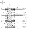
- the position of the connecting conductor on the outer layer on one side and the position of the connecting conductor on the outer layer on the other side are shifted in substantially the same direction from the position of the connecting conductor on the core substrate, and the connecting conductor on the inner layer is connected to the connecting conductor on the core substrate.
- the position of the connecting conductor on the outer layer on one side and the position of the connecting conductor on the outer layer on the other side are shifted in substantially the same direction from the position of the connecting conductor on the core substrate, and the connecting conductor on the inner layer is connected to the connecting conductor on the core substrate.
- FIG. 1 shows the example of the wiring board between the connection conductors of an outer layer. It is a figure which shows the 1st another example of the shape of the cross section of a via hole and a through hole. It is a figure which shows the 2nd another example of the shape of the cross section of a via hole and a through hole. It is a figure which shows the 3rd another example of the shape of the cross section of a via hole and a through hole. It is a figure which shows the example which combined the dissimilar figure about the via hole for forming a filled stack. It is a figure which shows another example of the dimensional relationship between the metal foil which comprises the land on a core insulating layer, and a via hole.
- FIG. 28A It is a figure which shows an example of the wiring board which incorporates an electronic component. It is a figure which shows an example of the wiring board by which the electronic component was mounted on the surface.
- arrows Z1 and Z2 indicate the stacking direction of the wiring boards corresponding to the normal direction (or the thickness direction of the core substrate) of the main surface (front and back surfaces) of the wiring boards, respectively.
- arrows X1, X2 and Y1, Y2 respectively indicate directions perpendicular to the stacking direction (directions parallel to the main surface of the wiring board).
- the main surface of the wiring board is an XY plane.
- the side surface of the wiring board is an XZ plane or a YZ plane.
- the cross section (XY plane) perpendicular to the Z direction is referred to as a transverse cross section.
- a cross section parallel to the Z direction (XZ plane or YZ plane) is referred to as a vertical cross section.
- the axis is a line parallel to the Z direction and passing through the center of the cross section (the center of gravity of each cross section other than the circle). That is, the Z direction generally corresponds to the axial direction.
- the two main surfaces facing the opposite normal directions are referred to as a first surface (Z1 side surface) and a second surface (Z2 side surface). That is, the main surface opposite to the first surface is the second surface, and the main surface opposite to the second surface is the first surface.
- the side closer to the core is referred to as the lower layer (or inner layer side), and the side far from the core is referred to as the upper layer (or outer layer side).
- a layer consisting only of a solid pattern is also called a conductor layer.
- a conductor formed in a hole penetrating the insulating layer is referred to as a connection conductor.
- the holes include via holes and through holes.
- a via hole is a hole that is formed, for example, by drilling in a state where there is a conductor layer (mainly a lower-layer conductor layer) on one side of the insulating layer, and reaches the conductor layer from the other side of the insulating layer.
- a conductor formed in a via hole (hereinafter referred to as a via conductor) is formed with a conductor layer on one side of the insulating layer, so that the via conductor and the conductor layer on at least one side of the insulating layer are not continuous. Thus, an interface is formed between the two.
- the through hole is a hole formed so as to penetrate the insulating layer including the conductor layer when the conductor layer is provided on one side or both sides of the insulating layer.
- the conductor formed in the through hole (hereinafter referred to as the through hole conductor) is usually formed together with the conductor layers on both sides of the insulating layer by plating or the like, so that the through hole conductor and the conductor layers on both sides of the insulating layer are formed. Is at least partially continuous.
- the conductor film formed on the walls (side and bottom surfaces) of the holes or notches is called conformal conductors and fills the holes or notches.
- the formed conductor is called a filled conductor.
- the conductor layer may include a land of a connection conductor.
- the plating refers to depositing a conductor (for example, metal) in a layered manner on the surface of metal or resin and the deposited conductor layer (for example, a metal layer).
- the plating includes dry plating such as PVD (Physical Vapor Deposition) and CVD (Chemical Vapor Deposition).
- the “width” of a hole or column (projection) means a diameter in the case of a circle, and 2 ⁇ (cross-sectional area / ⁇ ) otherwise.
- the most appropriate value is compared among the values, the average value, the maximum value, etc. of the corresponding portion in view of the action and effect. It is desirable to determine whether the “width” of the hole or protrusion matches or does not match (which is greater). However, this does not apply if the value to be compared is specified.
- the wiring board 100 of this embodiment is a printed wiring board.
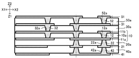
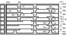
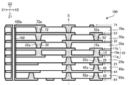
- the wiring board 100 includes a core substrate 10, insulating layers 20a, 30a, 40a, 50a, 60a, 70a, conductor layers 21, 31, 41, 51, 61, 71, And filled conductors 22, 32, 42, 52, 62, 72. That is, on the first surface side of the core substrate 10, the three insulating layers 20a, 40a, 60a and the three conductor layers 21, 41, 61 are alternately stacked. Further, on the second surface side of the core substrate 10, three insulating layers 30 a, 50 a, 70 a and three conductive layers 31, 51, 71 are alternately stacked.
- the core substrate 10 corresponds to a core portion.
- the insulating layers 20a to 70a and the like above the core portion correspond to a build-up portion.
- the core substrate 10 includes an insulating layer 10a (core insulating layer), conductor layers 11a and 11b, and a filled conductor 12.
- the thickness of the insulating layer 10a is, for example, 60 ⁇ m.
- the thickness of the conductor layers 11a and 11b will be described later.
- a via hole 12a penetrating the insulating layer 10a is formed in the insulating layer 10a.
- the filled conductor 12 is configured by filling the via hole 12a with plating.
- the filled conductor 12 corresponds to a connection conductor.
- the filled conductor 12 is a via conductor. Since the via conductor can be formed more easily than the through-hole conductor, such a structure is advantageous for cost reduction and the like.
- the present invention is not limited to this, and the filled conductor 12 may be a through-hole conductor (see FIGS. 23 and 24 described later).
- the insulating layer 10a is made of, for example, an epoxy resin.
- the epoxy resin preferably contains a reinforcing material such as glass fiber (for example, glass cloth or glass nonwoven fabric) or aramid fiber (for example, aramid nonwoven fabric) by, for example, resin impregnation treatment.
- the reinforcing material is a material having a smaller coefficient of thermal expansion than the main material (in the present embodiment, epoxy resin).
- the material of the insulating layer 10a is arbitrary.
- the conductor layers 11a and 11b are made of, for example, copper foil and copper plating.
- the filled conductor 12 is made of, for example, copper plating.
- the shape of the filled conductor 12 is, for example, a tapered cylinder (conical frustum) tapered so as to be reduced in diameter from the second surface side to the first surface side of the insulating layer 10a.
- the shape of the (Y plane) is, for example, a perfect circle.
- the present invention is not limited to this, and the shape of the filled conductor 12 is arbitrary (see FIGS. 18A to 21B described later).
- the conductor layers 11a and 11b have a three-layer structure of a metal foil, an electroless plating film, and an electrolytic plating film (see FIG. 22A described later).
- the structure of the conductor layers 11a and 11b is not limited to the above three-layer structure, and may be, for example, a two-layer structure of a metal foil and an electroless plating film or an electrolytic plating film (see FIG. 22B described later).
- the insulating layer 20 a is laminated on the first surface side of the core substrate 10, and the insulating layer 30 a is laminated on the second surface side of the core substrate 10.
- a conductor layer 21 is formed on the first surface of the insulating layer 20a, and a conductor layer 31 is formed on the second surface of the insulating layer 30a.
- An insulating layer 40a is stacked on the first surface side of the insulating layer 20a, and an insulating layer 50a is stacked on the second surface side of the insulating layer 30a.
- a conductor layer 41 is formed on the first surface of the insulating layer 40a, and a conductor layer 51 is formed on the second surface of the insulating layer 50a.
- an insulating layer 60a is stacked on the first surface side of the insulating layer 40a, and an insulating layer 70a is stacked on the second surface side of the insulating layer 50a.
- a conductor layer 61 is formed on the first surface of the insulating layer 60a, and a conductor layer 71 is formed on the second surface of the insulating layer 70a.
- the thickness of the insulating layers 20a, 30a, 40a, and 50a is, for example, 60 ⁇ m.
- the thickness of the insulating layers 60a and 70a is, for example, 50 ⁇ m.
- the thicknesses of the conductor layers 21, 31, 41, 51, 61, 71 will be described later.
- the conductor layers 21, 31, 41, 51, 61, 71 are made of, for example, copper foil and copper plating.
- the conductor layers 21, 31, 41, 51, 61, 71 have a three-layer structure of a metal foil, an electroless plating film, and an electrolytic plating film (see FIG. 22A described later).
- the structure of the conductor layers 21, 31, 41, 51, 61, 71 is not limited to the above three-layer structure, and may be, for example, a two-layer structure of a metal foil and an electroless plating film or an electrolytic plating film. (See FIG. 22B described later).
- the insulating layers 20a, 30a, 40a, 50a, 60a, and 70a correspond to interlayer insulating layers.
- the insulating layers 20a, 30a, 40a, 50a, 60a, and 70a are each formed by impregnating a core material with a resin.
- a core material for example, an inorganic material such as glass fiber or aramid fiber can be used.
- the resin for example, an epoxy resin, a polyester resin, a bismaleimide triazine resin (BT resin), an imide resin (polyimide), a phenol resin, or an allylated phenylene ether resin (A-PPE resin) can be used.
- the insulating layers 20a, 30a, 40a, 50a, 60a, and 70a are filled conductors 22, 32, 42, 52, 62, and 72 formed by filling the via holes 22a, 32a, 42a, 52a, 62a, and 72a with plating. Also have via conductors). Each of the filled conductors 22, 32, 42, 52, 62, 72 corresponds to a connection conductor.
- the filled conductors 22, 32, 42, 52, 62, 72 are made of, for example, copper plating.
- the shape of the filled conductors 22, 42, 62 is, for example, a tapered cylinder (conical frustum) tapered so as to be reduced in diameter from the first surface side to the second surface side of the insulating layer 10a.
- the shape of the cross section (XY plane) is, for example, a perfect circle.
- the filled conductors 32, 52, and 72 are, for example, tapered cylinders (conical frustums) tapered so as to be reduced in diameter from the second surface side to the first surface side of the insulating layer 10a. , 52, 72 have a cross-sectional shape (XY plane), for example, a perfect circle.
- the present invention is not limited to this, and the shape of the filled conductor 22 and the like is arbitrary (see FIGS. 18A to 21B described later).
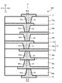
- the filled conductor 12 of the core portion (core substrate 10) and the filled conductors 22, 32, 42, 52, 62, and 72 of the buildup portion are stacked on, for example, the same axis (Z axis). .
- Z axis the same axis
- the filled stack S is extended along the Z direction by the filled conductors 12 and the like that are stacked. Adjacent filled conductors are in close contact (contact) and are electrically connected to each other.
- the filled stack S electrically connects the conductor layers on both sides of the wiring board 100, that is, the conductor layer 61 on the first surface and the conductor layer 71 on the second surface.
- the filled stack S has a so-called full stack structure in which filled conductors of all layers are stacked. For this reason, it becomes easy to secure the wiring space, and the degree of freedom in designing the wiring pattern is increased. Further, since the wiring in the X direction or the Y direction can be omitted, the wiring length in the interlayer connection can be shortened.
- the arrangement and number of filled stacks S are arbitrary. For example, there may be a plurality of filled stacks S (see FIGS. 28A and 28B described later).
- a through hole 102a penetrating all layers is formed, and a conformal conductor 102 (through hole conductor) made of, for example, plating is formed on the wall surface of the through hole 102a. That is, the through hole 102a penetrates the wiring board 100 in the Z direction (stacking direction).
- the conformal conductor 102 electrically connects the conductor layer 61 and the conductor layer 71.
- the conformal conductor 102 may be electrically connected to the ground line or the like of the wiring board 100, or may be electrically isolated from all other conductors.
- the structure of the conformal conductor 102 is, for example, a two-layer structure of an electroless plating film and an electrolytic plating film.
- the structure of the conformal conductor 102 is not limited to this and is arbitrary.
- the conformal conductor 102 made of only an electroless plating film or only an electroplating film may be used.
- the conformal conductor 102 has a conductor only on the wall surface of the through hole 102a. Therefore, a cavity is formed in the through hole 102a, and the distortion of the wiring board 100 is reduced. It becomes easy to be done.
- the present invention is not limited to this, and a filled conductor may be used instead of the conformal conductor 102.
- the shape of the through hole 102a is, for example, a cylinder, and the opening shape of the through hole 102a is, for example, an ellipse. It is considered that the strength of a wide region in the XY plane can be effectively improved by the oval shape of the through hole 102a.
- the through hole 102a is arranged at the peripheral edge of the wiring board 100, for example.
- the number of through holes 102a, the opening shape, the arrangement, and the like are arbitrary.
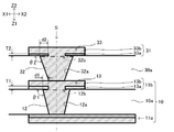
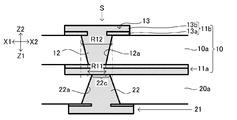
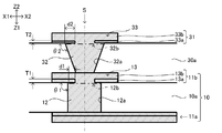
- FIG. 3 shows an enlarged view of a portion of FIG. 1, more specifically, the filled conductor 12 of the core substrate 10 and the filled conductor 32 stacked on the second surface thereof.
- FIG. 3 illustrates the relationship between the land 13 on the insulating layer 10a of the core substrate 10 and the land 33 on the insulating layer 30a (interlayer insulating layer). The relationship between the land on the layers 20a, 40a, 50a, 60a, and 70a and the land 13 is the same.
- the conductor layer 11b includes the land 13 of the filled conductor 12, and the conductor layer 31 includes the land 33 of the filled conductor 32.
- the thickness of the conductor layers 11a and 11b of the core substrate 10 is 18 ⁇ m, for example.
- the thickness of the conductor layers 21, 31, 41, 51 laminated on both surfaces of the core substrate 10 is, for example, 18 ⁇ m.
- the thickness of the outermost conductor layers 61 and 71 is, for example, 25 ⁇ m.
- the land 13 is formed on the insulating layer 10a (second surface side), and the land 33 is formed on the insulating layer 30a.
- the land 13 includes a metal foil 13a (for example, a copper foil) and, for example, a copper plating film 13b formed on the metal foil 13a.
- the land 33 includes a metal foil 33a (for example, a copper foil) and, for example, a copper plating film 33b formed on the metal foil 33a.
- the thickness of each said conductor layer corresponds to the sum total of the thickness of metal foil, and the thickness of a plating film.
- the metal foil 13a constituting the land 13 (land on the core insulating layer) is replaced with the metal foil 33a constituting the land 33 on the insulating layer 30a (interlayer insulating layer on the core insulating layer). Thicker than. According to such a structure, it is considered that the thermal stress around the core is relaxed by the metal foil 13a because the metal foil 13a of the core substrate 10 is thick (details will be described later).
- the thickness T1 of the metal foil 13a is preferably 5 ⁇ m or more, for example, 7.5 ⁇ m.
- the thickness T2 of the metal foil 33a is preferably 4.5 ⁇ m or less, for example, 4.5 ⁇ m.
- the metal foils 13a and 33a having such dimensions can be formed using a thin copper foil, but can also be formed by adjusting the thickness by etching using a thick copper foil. For example, if the thickness of the metal foils 1001 and 1002 of the double-sided copper-clad laminate 1000 (see FIG. 9A described later) as a starting material is 5 ⁇ m or more, a step of forming the filled conductor 12 (see FIGS. 9B and 9C described later). ) And the like, it is considered that the handling property of the double-sided copper-clad laminate 1000 is excellent (for details, see the description of the manufacturing process described later).
- the plating film 13b constituting the land 13 is thinner than the plating film 33b constituting the land 33 on the insulating layer 30a (interlayer insulating layer on the core insulating layer). According to such a structure, since the plating film 13b of the core substrate 10 is thin, the plating time for obtaining a necessary conductor thickness in the manufacture of the core substrate 10 is shortened. As a result, it is considered that the production efficiency of the core substrate 10 can be improved.
- the diameter of the opening 12b on the second surface side (expansion side) of the via hole 12a is, for example, 75 ⁇ m
- the diameter of the opening 32b on the second surface side (expansion side) of the via hole 32a is, for example, 75 ⁇ m.
- the diameter reduction angle ⁇ 2 of the insulating layer 30a (interlayer insulating layer on the core insulating layer) to the first surface side (reduced diameter side) in the opening 32b on the second surface side (expanded diameter side) of the via hole 32a is expressed by the insulating layer It is larger than the diameter reduction angle ⁇ 1 to the first surface side (reduction diameter side) in the opening 12b on the second surface side (expansion side) of the via hole 12a of 10a.
- the degree of taper of the via hole 12a of the core substrate 10 is gentler than the degree of taper of the via hole 32a of the build-up portion, so that heat cycle is performed around the core where stress is likely to concentrate (details will be described later). It is thought that the thermal stress due to is relaxed. As a result, it is considered that the connection reliability between the filled conductor 12 of the core substrate 10 and the filled conductor 32 of the insulating layer 30a can be improved.
- the diameter reduction angle ⁇ 1 is, for example, about 110 °, and the diameter reduction angle ⁇ 2 is, for example, about 95 °.
- the difference ( ⁇ 1 ⁇ 2) between the diameter reduction angle ⁇ 1 and the diameter reduction angle ⁇ 2 is, for example, about 15 °.
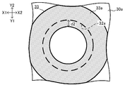
- the amount of protrusion (protrusion amount d1) of the metal foil 13a constituting the land 13 (land on the core insulating layer) inward from the edge of the via hole 12a is the insulating layer.
- the metal foil 33a constituting the land 33 on 30a (interlayer insulating layer on the core insulating layer) is smaller than the amount projecting inward from the edge of the via hole 32a (projecting amount d2).
- the protrusion amount d1 of the metal foil 13a on the core substrate 10 is smaller than the protrusion amount d2 of the metal foil 33a on the insulating layer 30a of the buildup portion, so that the stress around the core where stress tends to concentrate ( It is considered that corner cracks in details (to be described later) can be effectively reduced.
- the protrusion amount d1 is, for example, about 8.4 ⁇ m
- the protrusion amount d2 is, for example, about 13 ⁇ m.
- the difference (d2 ⁇ d1) between the protrusion amount d1 and the protrusion amount d2 is, for example, about 4.6 ⁇ m.
- the protruding amounts d1 and d2 are substantially constant in the circumferential direction of the via holes 12a and 32a, respectively.
- the present invention is not limited to this, and the protruding amounts d1 and d2 may not be substantially constant in the circumferential direction of the via holes 12a and 32a (see FIGS. 20A and 20B described later).
- the filled conductor 12 via conductor of the core insulating layer
- the filled conductor 32 via conductor of the interlayer insulating layer
- a land 13 composed of a metal foil 13a and a plating film 13b formed on the metal foil 13a is formed.
- the insulating layer 30a interlayer insulating layer on the core insulating layer
- a land 33 composed of a metal foil 33a and a plating film 33b formed on the metal foil 33a is formed.
- the metal foil 13a is thicker than the metal foil 33a.
- the metal foil (especially copper foil) is considered to be more easily stretched than the plating (particularly copper plating), and the thermal stress applied in a superimposed manner by the heat cycle is concentrated on the core (core substrate 10) (details). Is considered later).
- the metal foil 13a of the core substrate 10 is thick as described above, it is considered that the thermal stress around the core is relaxed by the metal foil 13a. As a result, it is presumed that the wiring board 100 becomes stronger against the thermal stress.
- the metal foil 13a constituting the land 13 on the second surface side of the insulating layer 10a is a metal foil on the insulating layer 30a on the upper layer (second surface side).
- the metal foil constituting the land on the first surface side of the insulating layer 10a may be thicker than the metal foil on the insulating layer 20a on the upper layer (first surface side) (described later).
- a conformal conductor 102 (through-hole conductor) is formed on the wall surface of the through-hole 102a that penetrates all layers of the wiring board 100. This conformal conductor 102 is considered to be strong against stress in the Z direction.
- the above structure is more useful as the number of wiring board layers (number of conductor layers) increases.
- three or more conductor layers and three or more insulating layers are alternately laminated on both sides of the core substrate. It is effective to apply to a wiring board having 8 layers (number of conductor layers) or more.
- this will be described with reference to FIGS.
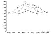
- FIG. 5 and FIG. 6 show the results of simulation of stress (especially thermal stress due to heat cycle) applied to the 6-layer, 8-layer, and 10-layer wiring boards (6-layer product, 8-layer product, 10-layer product) Show.
- the 6-layer product, the 8-layer product, and the 10-layer product all have a full stack structure.
- a line L1 is data related to a 6-layer product
- a line L2 is data related to an 8-layer product
- a line L3 is data related to a 10-layer product.
- the stress applied to the core is the largest, and the stress decreases as the distance from the core increases. Further, when the stress applied to each of the 6-layer product, the 8-layer product, and the 10-layer product is compared, the stress in the 10-layer product is the largest, the stress in the 8-layer product is the next largest, and the stress in the 6-layer product is the smallest. . From this, it is surmised that the stress in the wiring board increases as the number of layers increases.
- FIG. 7 shows the result of simulation of the crack occupancy in each layer of the 8-layer product and the 10-layer product.
- cracks also occur in the first stage (insulating layer on the core substrate). Therefore, if the via conductor of the core substrate is simply reinforced, there is a concern that the concentration of cracks may occur in the upper (first stage) via conductor. Further, as described above, it is considered that the stress in the wiring board increases as the number of layers increases. Therefore, the occurrence of cracks around the core is considered to become more serious as the number of layers of the wiring board increases.
- the metal foil 13a of the core substrate 10 is thick as described above, so that the thermal stress around the core is relaxed by the metal foil 13a, and It is thought that the occurrence of cracks is suppressed.
- the wiring board 100 of the present embodiment is an eight-layer wiring board (conductor layers 11a, 11b, 21, 31, 41, 51, 61, 71).
- the present invention is not limited to this, and a wiring board having nine or more layers (for example, a ten-layer wiring board) may be used.
- the wiring board 100 is manufactured, for example, according to the procedure shown in FIG.
- step S10 the core substrate 10 is prepared.
- 9A to 9D show a manufacturing method of the core substrate 10.
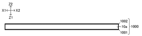
- a double-sided copper-clad laminate 1000 (starting material) is prepared.
- the double-sided copper-clad laminate 1000 includes an insulating layer 10a and metal foils 1001 and 1002 (for example, copper foil).
- a metal foil 1001 is formed on the first surface of the insulating layer 10a, and a metal foil 1002 is formed on the second surface of the insulating layer 10a.
- the material of the insulating layer 10a is, for example, an epoxy resin containing a reinforcing material.
- the metal foil 1002 becomes a metal foil 13a (FIGS. 3 and 4A) by patterning in a later process (FIG. 9D).
- a metal foil 1002 having a predetermined thickness for example, 7.5 ⁇ m
- the method is not limited to this, and the method for forming the metal foil 1002 is arbitrary.
- a metal foil 1002 having a predetermined thickness may be obtained by attaching a relatively thick (for example, 12 ⁇ m) metal foil to the insulating layer and then half-etching the metal foil.
- the thickness of the metal foils 1001 and 1002 of the double-sided copper-clad laminate 1000 as a starting material is 5 ⁇ m or more. By setting it as such a dimension, the intensity
- the thicknesses of the metal foils 1001 and 1002 are not limited to this range, and may be changed as appropriate.
- via holes 12a are formed in the insulating layer 10a by, for example, a laser.
- the via hole 12a penetrates the metal foil 1002 and the insulating layer 10a, but does not penetrate to the metal foil 1001. Thereby, a via hole 12a extending from the second surface side of the insulating layer 10a to the metal foil 1001 is formed. Then, desmear or soft etch is performed as necessary.
- plating 1003 is formed on the first surface of the metal foil 1001 by, for example, copper panel plating (plating on the via hole 12a and entire plating), and on the second surface of the metal foil 1002.
- plating 1004 is formed in the via hole 12a.
- the plating 1004 is filled in the via hole 12a.
- a filled conductor 12 is formed.
- the plating 1003 and 1004 are formed, for example, by first performing electroless plating and then performing electrolytic plating using the electroless plating film as a cathode (see FIG. 22A described later).
- a plating solution for electroless plating for example, a copper sulfate solution to which a reducing agent or the like is added can be used.
- a plating solution for electrolytic plating for example, a copper sulfate solution, a copper pyrophosphate solution, a blue (cyanide) copper solution, or a copper borofluoride solution can be used.
- the conductive layers on both sides of the insulating layer 10a are patterned by, for example, a lithography technique. Thereby, the conductor layer 11a is formed on the first surface of the insulating layer 10a, and the conductor layer 11b is formed on the second surface of the insulating layer 10a. As a result, the core substrate 10 is completed.
- step S ⁇ b> 11 of FIG. 8 an insulating layer and a metal foil are formed on both sides of the core substrate 10.
- a metal foil 1005 for example, copper foil
- an insulating layer 20a for example, a core substrate 10
- an insulating layer 30a for example, a metal foil 1006 (for example, copper foil) are formed from the first surface side. Arrange in order. Thereby, a laminated body is formed. In this laminated body, the core substrate 10 is sandwiched between the insulating layers 20a and 30a, and these are further sandwiched between the metal foil 1005 and the metal foil 1006.
- the insulating layers 20a and 30a are prepregs (semi-cured adhesive sheets). However, RCF (Resin Coated copper Foil) or the like can be used instead of the prepreg.
- the metal foils 1005 and 1006 are half-etched.
- the metal foil 1006 becomes the metal foil 33a (FIGS. 3 and 4B) by patterning in the subsequent process (FIG. 10D).
- the metal foil 1006 having a predetermined thickness (for example, 4.5 ⁇ m) is obtained by half-etching before pressing described later.
- a metal foil 1006 having a predetermined thickness may be attached from the beginning by laminating or the like, but it is difficult to attach a thin metal foil to the insulating layer.
- the metal foil after a relatively thick metal foil (for example, 7.5 ⁇ m having the same thickness as the metal foil 1002) is attached to the insulating layer, the metal foil has a predetermined thickness (for example, 4.5 ⁇ m).
- a high-quality metal foil 1006 can be easily obtained.
- the method for forming the metal foil 1006 is not limited to this, and any method can be used.
- a metal foil 1006 having a predetermined thickness for example, 4.5 ⁇ m
- the laminate is heated and pressed in the Z direction. That is, pressing and heat treatment are performed simultaneously.
- the prepreg (insulating layers 20a and 30a) is cured by pressing and heating, and the members adhere to each other. As a result, the laminate is integrated. Note that the pressing and heat treatment may be performed in a plurality of times.
- heat processing and a press may be performed separately, it is more efficient to perform it simultaneously. You may perform the heat processing for integration separately after a heat press.
- step S ⁇ b> 12 of FIG. 8 via holes are formed in the insulating layer on both sides of the core substrate 10.
- via holes 22a are formed in the insulating layer 20a and via holes 32a are formed in the insulating layer 30a by, for example, a laser.
- the via holes 22a and 32a for forming the filled stack S are formed on the same axis (Z axis) as the filled conductor 12 constituting the filled stack S.
- desmear or soft etch is performed as necessary.
- step S13 of FIG. 8 plating is performed.
- plating 1007 is formed on the first surface of the metal foil 1005 and in the via hole 22a by, for example, copper panel plating, and then on the second surface of the metal foil 1006 and in the via hole 32a.
- a plating 1008 is formed.
- the plating 1007 and 1008 are formed by performing electroless plating first, and subsequently performing electroplating using the electroless plating film as a cathode, as in the process of FIG. 9C (see FIG. 22A described later).
- the via holes 22a and 32a are filled with plating 1007 and 1008, respectively.
- filled conductors 22 and 32 are formed.
- the filled conductors 22 and 32 constituting the filled stack S are stacked on the same axis (Z axis) as the other filled conductors 12 constituting the filled stack S.
- step S14 of FIG. 8 the conductor layer is patterned.
- the conductive layers on both sides are patterned by lithography, for example.
- the conductor layer 21 is formed on the first surface of the insulating layer 20a
- the conductor layer 31 is formed on the second surface of the insulating layer 30a.
- step S15 of FIG. 8 by repeating steps S11 to S14, as shown in FIG. 11, insulating layers 40a and 50a, via holes 42a and 52a, filled conductors 42 and 52, and conductor layers 41 and 51 is formed.
- the filled conductors 42 and 52 constituting the filled stack S are stacked on the same axis (Z axis) as the other filled conductors 12 constituting the filled stack S and the like.
- step S ⁇ b> 16 of FIG. 8 an insulating layer and a metal foil are formed on both sides of the core substrate 10.
- an insulating layer 60 a and a metal foil 1009 are laminated on the first surface side of the core substrate 10, and insulation is performed on the second surface side of the core substrate 10.
- the layer 70a and the metal foil 1010 are laminated.
- metal foils 1009 and 1010 are half-etched as necessary.
- this laminate is heated and pressed in the Z direction.
- the prepreg (insulating layers 60a and 70a) is cured and the members adhere to each other.
- the laminate is integrated.
- the pressing and heat treatment may be performed in a plurality of times.
- heat processing and a press may be performed separately, it is more efficient to perform it simultaneously. You may perform the heat processing for integration separately after a heat press.
- step S17 in FIG. 8 via holes are formed in the insulating layer on both sides of the core substrate 10, and through holes penetrating all the layers are formed.
- a via hole 62a that penetrates the insulating layer 60a, a via hole 72a that penetrates the insulating layer 70a, and a through hole 102a that penetrates all layers are formed by, for example, a laser.
- the via holes 62a and 72a for forming the filled stack S are formed on the same axis (Z axis) as the filled conductor 12 and the like constituting the filled stack S.
- desmear or soft etch is performed as necessary.
- the entire surface of the irradiated object is irradiated with laser light in a state where a light-shielding mask is provided.
- the present invention is not limited to this, and the laser irradiation may be stopped in the non-irradiated portion without using the light shielding mask, and the laser beam may be irradiated only on the portion to be irradiated.
- the via holes 62a and 72a and the through hole 102a can be formed by one scan.
- the laser intensity is preferably adjusted by pulse control.
- the number of shots (number of irradiations) is changed without changing the laser intensity per shot (one irradiation). That is, when the desired laser intensity cannot be obtained with one shot, the same irradiation position is irradiated with laser light again.
- the via hole 12a (FIG. 9B) in the core part is formed by two shots, and the via holes 22a, 32a, 42a, 52a, 62a, 72a in the buildup part are formed by one shot. In the formation of the through hole 102a, the number of shots is further increased.
- the time for changing the irradiation condition can be omitted, and it is considered that the throughput is improved.
- the method is not limited to this, and the laser intensity adjustment method is arbitrary.
- the irradiation conditions may be determined for each irradiation position, and the number of irradiations may be constant (for example, one shot per irradiation position).
- the through hole 102a can be formed by irradiating laser light from only one side of the core substrate 10 or by irradiating laser light from both sides of the core substrate 10 simultaneously.
- a through hole 102a is formed by irradiating the laser beam from the other side to penetrate the bottom. May be.
- step S18 of FIG. 8 plating is performed.
- the plating 1011 is formed.
- the plating 1011 is formed, for example, by performing electroless plating first, and subsequently performing electroplating using the electroless plating film as a cathode, as in the process of FIG. 9C (see FIG. 22A described later).
- the via holes 62a and 72a are filled with the plating 1011, and the plating 1011 is also formed on the wall surface of the through hole 102a.
- filled conductors 62 and 72 and conformal conductor 102 are formed.
- the filled conductors 62 and 72 constituting the filled stack S are stacked on the same axis (Z axis) as other filled conductors 12 constituting the filled stack S and the like.
- the formation of the plating 1011 on the wall surface of the through hole 102a and the formation of the plating 1011 on the outermost via holes (via holes 62a and 72a) are performed simultaneously. For this reason, it is thought that reduction of the number of processes and by extension, cost reduction can be achieved.
- step S19 of FIG. 8 the conductive layers on both sides are patterned by lithography, for example.
- the conductor layer 61 is formed on the first surface of the insulating layer 60a
- the conductor layer 71 is formed on the second surface of the insulating layer 70a.
- the wiring board 100 is completed.
- the wiring board 100 can be connected to other wiring boards or electronic components can be mounted on the wiring board 100 through the external connection terminals. (See FIG. 30 described later).
- each conductor layer may be formed by a method of selectively plating only a pattern portion using a plating resist, that is, a so-called pattern plating method.
- the filled conductors 12 constituting the filled stack S are stacked on the same axis (Z axis).
- the filled conductors 12 and the like may be stacked while being shifted in the X direction or the Y direction.
- a range R11 is an opening range on the first surface side of the via hole 12a
- a range R12 is an opening range on the second surface side of the via hole 12a.
- the lower layer side (first surface side) of the filled conductor 32 is used.
- the other end (outer end) may be disposed within the range R12 outside the range R11.
- one end (inner end) of the end surface 32c may be disposed within the range R11, and the other end (outer end) may be disposed outside the range R12.
- FIG. 14B one end (inner end) of the end surface 32c may be disposed within the range R11, and the other end (outer end) may be disposed outside the range R12.
- one end (inner end) of the end surface 32c may be disposed outside the range R11 and within the range R12, and the other end (outer end) may be disposed outside the range R12. .
- the filled conductor 52 is stacked on the second surface side of the filled conductor 32, and when the filled conductor 72 is stacked on the second surface side of the filled conductor 52, the filled conductor 22 is formed on the first surface side of the filled conductor 12.
- the filled conductors 42 are stacked on the first surface side of the filled conductor 22 or the filled conductor 62 is stacked on the first surface side of the filled conductor 42.
- the filled conductors whose taper directions are reversed are stacked, for example, when the filled conductor 22 is stacked on the first surface side of the filled conductor 12, as shown in FIG.
- One end (inner end) of the end surface 22c on the second surface side may be disposed within the range R11, and the other end (outer end) may be disposed within the range R12 outside the range R11.
- one end (inner end) of the end face 22c may be arranged within the range R11, and the other end (outer end) may be arranged outside the range R12.
- one end (inner end) of the end face 22c may be disposed outside the range R11 and within the range R12, and the other end (outer end) may be disposed outside the range R12. .
- At least each filled conductor is stacked.
- being stacked means that at least one end (inner end) of the lower layer side end face of the filled conductor is within an opening range on at least one side of a hole formed in the lower layer.
- the positions of filled conductors 62 and 72 are shifted from the position of filled conductor 12 (connection conductor of core substrate 10) in substantially the same direction on both sides of core substrate 10. It is preferable.
- the position of the filled conductor 62 on the first surface side and the position of the filled conductor 72 on the second surface side are both shifted from the position of the filled conductor 12 to the X2 side. That is, the position of the filled conductor 62 and the position of the filled conductor 72 are shifted in the same direction.
- Such a structure can also be expected to have the effect of suppressing the occurrence of cracks around the core as described above.
- the inner layer connection conductors in the build-up portion are arranged between the connection conductors of the core substrate 10 and the outer layer connection conductors on both sides of the core substrate 10.
- the filled conductors 22 and 42 are connected to the filled conductor 12 (connection conductor of the core substrate 10) in the shift direction (X direction) of the filled conductor 62. It is arranged between the conductor 62 (outer layer connection conductor on the first surface side) (range R21).
- the filled conductors 32 and 52 are connected to the filled conductor 12 (connection conductor of the core substrate 10) and the filled conductor 72 (second conductor) in the shift direction (X direction) of the filled conductor 72. (Range R22).
- the filled conductors 42 and 52 are arranged outside the ranges R21 and R22 (see FIG. 16).
- such an arrangement is not an essential configuration.
- the shape of the via hole, through hole, or land cross section (XY plane) in each layer is arbitrary.
- the shape of these surfaces may be a regular circle as shown in FIG. 18A in addition to a perfect circle, or may be another regular polygon such as a regular hexagon or a regular octagon.
- the shape of the polygonal corner is arbitrary, and may be, for example, a right angle, an acute angle, an obtuse angle, or rounded. However, in order to prevent concentration of thermal stress, it is preferable that the corners are rounded.
- the shape of the cross section may be an ellipse, a rectangle, a triangle, or the like. Furthermore, as shown in FIG. 18B or FIG. 18C, a shape in which a straight line is drawn radially from the center, such as a cross shape or a regular polygonal star shape (a shape in which a plurality of blades are arranged radially) is also effective as the shape of the cross section. It is.
- the above shapes may be arbitrarily combined.
- non-similar figures may be combined.
- the cross-section of the connecting conductor and the cross-section of the land may be made into non-similar figures.
- the cross section of the via holes 12a and 32a may be a regular polygonal star
- the cross section of the lands 13 and 33 may be a perfect circle.
- the protruding amounts d1 and d2 are not substantially constant in the circumferential direction of the via holes 12a and 32a, respectively. Therefore, for example, if the average value of the protrusion amount d1 is made smaller than the average value of the protrusion amount d2, it is considered that corner cracks around the core can be effectively reduced as described above.
- the shape of the vertical cross-section of via holes and through holes in each layer is also arbitrary.
- the shape of the via hole 12a and the filled conductor 12 in the core may be a cylinder.
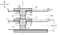
- the via holes 12a and 32a and the filled conductors 12 and 32 may have a drum shape.
- the width of the narrow portion N located between the openings on the first surface and the second surface is smaller than the width of the openings on both sides thereof, so that it is considered that the plating fillability is improved.
- the flatness of the surface is considered to increase.
- the side surfaces of the filled conductors 12 and 32 become inclined surfaces, it is considered that the adhesive strength between them is improved.
- the via holes 22a, 42a, 52a, 62a, 72a, and the through holes 102a may have a drum shape.
- the diameter reduction angle ⁇ 1 of the via hole 12a of the core substrate 10 is set to be smaller than that of the via hole 32a of the buildup portion.
- the shape of the via hole 12a in the core part and the shape of the via hole 22a in the build-up part may be a cylinder.
- the shape of the through hole 102a or the like may be the above cylinder or hourglass shape.
- the structure of the conductor layer in each layer is not limited to the above three-layer structure, and may be, for example, a two-layer structure of a metal foil and an electroless plating film or an electrolytic plating film.
- the structure of the filled conductor in each layer is not limited to the two-layer structure of the electroless plating film and the electrolytic plating film, and may be a structure including only the electroless plating film or the electrolytic plating film, for example.
- the structure of the conductor layer 11a and the like is formed on the insulating layer 2001 on the insulating layer 2001, such as the conductor layer 2004 shown in FIG. 22A, and the electroless plating film 2003a of copper, for example.
- the filled conductor 22 and the like have a two-layer structure of an electroless plating film 2003a and an electrolytic plating 2003b as in the filled conductor 2005 shown in FIG. 22A.
- the present invention is not limited to this, and the structure of the conductor layer 11a and the like may be a two-layer structure in which the electroless plating film 2003a is omitted, for example, a conductor layer 2004 shown in FIG. 22B.
- the structure of the filled conductor 22 and the like may be a structure including only electrolytic plating 2003b.
- the conformal conductor 102 (through-hole conductor) can also have the same structure. Note that omitting the electroless plating film 2003a and the like may cause a decrease in the adhesion of the conductor layer. Therefore, if necessary, a surface treatment for improving the adhesion may be performed on the insulating layer 2001 (insulating layer 10a). Etc.).
- the filled conductor 12 is not limited to a via conductor.
- the filled conductor 12 may be a through-hole conductor.
- the filled conductor 12 and the conductor layers 11a and 11b on both sides of the insulating layer 10a are continuous at least partially (for example, a plating portion).
- the filled conductor 12 is configured by filling a through hole 12c with plating.
- Such a filled conductor 12 (through-hole conductor) can be formed by, for example, performing immersion plating after forming the through-hole 12c in the insulating layer 10a.
- the drum-shaped through hole 12c is illustrated, but the shape of the through hole 12c is arbitrary.
- the through hole 12c can be formed by irradiating laser light from only one side of the core substrate 10 or by irradiating laser light from both sides of the core substrate 10 simultaneously. Further, after forming a bottomed hole (non-through hole) by irradiating a laser beam from one side of the core substrate 10, a through hole 12c is formed by irradiating the laser beam from the other side and penetrating the bottom. May be.
- the conductor layer 11a includes the land 14 of the filled conductor 12, and the conductor layer 21 includes the land 23 of the filled conductor 22.
- the land 14 is formed on the insulating layer 10a (first surface side), and the land 23 is formed on the insulating layer 20a.
- the land 14 includes a metal foil 14a (for example, a copper foil) and, for example, a copper plating film 14b formed on the metal foil 14a.
- the land 23 includes a metal foil 23a (for example, a copper foil) and, for example, a copper plating film 23b formed on the metal foil 23a.
- the thickness of each said conductor layer corresponds to the sum total of the thickness of metal foil, and the thickness of a plating film.
- the metal foil 14a constituting the land 14 on the first surface side of the insulating layer 10a is preferably thicker than the metal foil 23a constituting the land 23 on the insulating layer 20a on the upper layer (first surface side). . According to such a structure, since the metal foil 14a of the core substrate 10 is thick, it is considered that the thermal stress around the core is relieved by the metal foil 14a as in the above embodiment. Further, as in the above embodiment, if the metal foils 13a and 33a on the second surface side have the same relationship, a synergistic effect can be expected.
- the thickness T3 of the metal foil 14a is preferably 5 ⁇ m or more, for example, 7.5 ⁇ m.
- the thickness T4 of the metal foil 23a is preferably 4.5 ⁇ m or less, for example, 4.5 ⁇ m.
- the metal foils 14a and 23a having such dimensions can be formed using a thin copper foil, but can also be formed by adjusting the thickness by etching using a thick copper foil.
- the plating film 14b constituting the land 14 is thinner than the plating film 23b constituting the land 23 on the insulating layer 20a (interlayer insulating layer on the core insulating layer).
- the plating film 14b of the core substrate 10 is thin, in the manufacture of the core substrate 10, the plating time for obtaining a necessary conductor thickness is shortened. As a result, it is considered that the production efficiency of the core substrate 10 can be improved.
- the plating films 13b and 33b on the second surface side have the same relationship, a synergistic effect can be expected.
- the diameter of the through hole 12c of 10a is larger than the diameter reduction angle ⁇ 3 to the second surface side in the opening portion 12d on the first surface side.
- the degree of taper of the through hole 12c of the core substrate 10 is gentler than the degree of taper of the via hole 22a in the build-up portion. Is expected to be eased.
- the connection reliability between the filled conductor 12 of the core substrate 10 and the filled conductor 22 of the insulating layer 20a can be improved.
- the diameter-reduction angles ⁇ 1 and ⁇ 2 on the second surface side have the same relationship as in the above embodiment, a synergistic effect can be expected.
- the amount of protrusion (projection amount d3) of the metal foil 13a constituting the land 13 (land on the core insulating layer) inward from the edge of the through hole 12c is the insulating layer 20a (interlayer insulation on the core insulating layer).
- the metal foil 23a constituting the land 23 on the layer) is smaller than the amount projecting inward from the edge of the via hole 22a (projection amount d4).
- the amount of protrusion d3 of the metal foil 14a on the core substrate 10 is smaller than the amount of protrusion d4 of the metal foil 23a on the insulating layer 20a in the build-up portion, thereby effectively causing corner cracks around the core. Can be mitigated.
- the protrusion amounts d1 and d2 on the second surface side have the same relationship, a synergistic effect can be expected.
- FIG. 24 shows an example of dimensions for the example of FIG.
- the diameter of the opening 12d on the first surface side and the opening 12b on the second surface side of the via hole 12a is, for example, 75 ⁇ m
- the diameter of the opening 22b on the first surface side of the via hole 22a is, for example, 75 ⁇ m.
- the diameter of the opening 32b on the second surface side of 32a is, for example, 75 ⁇ m.
- the diameter reduction angles ⁇ 1 and ⁇ 3 are about 110 °, for example, and the diameter reduction angles ⁇ 2 and ⁇ 4 are about 120 °, for example.
- the protruding amounts d1 and d3 are, for example, about 6.5 ⁇ m
- the protruding amounts d2, d4 are, for example, about 22 ⁇ m.
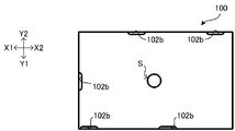
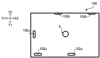
- a notch 102b penetrating the wiring board 100 in the Z direction (stacking direction) may be used instead of the through hole 102a.
- the notch 102 b is formed on the side surface of the wiring board 100.
- a conformal conductor 102 (see FIG. 1) is formed on the wall surface of the notch 102b.
- a through hole 102a and a notch 102b may be used in combination.
- the notch 102b can be formed by dividing (cutting) the through hole 102a along the line L10 after forming the through hole 102a.
- the method is not limited to this, and the method of forming the notch 102b is arbitrary.
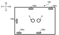
- the number of filled stacks S is not limited to one and is arbitrary.
- the wiring board 100 may have a plurality of (for example, two) filled stacks S.
- the wiring board 100 may have an electronic component and be an electronic device.
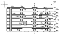
- an electronic component 3001 may be built in the wiring board 100.
- two electronic components 3001 are incorporated, but the number of electronic components is arbitrary.
- only one electronic component may be built in the wiring board 100.
- the wiring board 100 incorporating the electronic component it is possible to enhance the functionality of the electronic device.
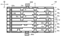
- an electronic component 3002 may be mounted on the surface of the wiring board 100.
- the electronic components 3002 are mounted on both sides of the wiring board 100, but the electronic components 3002 may be mounted only on one side of the wiring board 100.
- the number of electronic components is arbitrary. For example, only one electronic component may be mounted on the wiring board 100.
- the configuration of the wiring board 100 and the types, performances, dimensions, materials, shapes, number of layers, or arrangement of the components can be arbitrarily changed without departing from the spirit of the present invention. it can.
- the number of layers of the wiring board 100 is arbitrary. For example, in order to achieve high functionality, for example, after the structure shown in FIG. 1 is completed, further lamination may be continued to form a multilayer wiring board.
- each conductor layer is not limited to the above, and can be changed according to the application. For example, you may use metals other than copper as a material of a conductor layer.
- the material of each insulating layer is also arbitrary.
- the resin constituting the insulating layer is preferably a thermosetting resin or a thermoplastic resin.
- the thermosetting resin for example, imide resin (polyimide), BT resin, allylated phenylene ether resin (A-PPE resin), aramid resin and the like can be used in addition to the above-described epoxy resin.
- a thermoplastic resin liquid crystal polymer (LCP), PEEK resin, PTFE resin (fluorine resin) etc. can be used, for example.
- each conductor layer and each insulating layer may be composed of a plurality of layers made of different materials.
- the wiring board according to the present invention is suitable for a circuit board of an electronic device. Moreover, the method for manufacturing a wiring board according to the present invention is suitable for manufacturing a circuit board of an electronic device.
Landscapes
- Engineering & Computer Science (AREA)
- Manufacturing & Machinery (AREA)
- Microelectronics & Electronic Packaging (AREA)
- Production Of Multi-Layered Print Wiring Board (AREA)
- Printing Elements For Providing Electric Connections Between Printed Circuits (AREA)
Abstract
Description
10a 絶縁層
11a、11b 導体層
12 フィルド導体(接続導体)
12a ビアホール
12b 開口部
12c スルーホール
12d 開口部
13 ランド
13a 金属箔
13b めっき膜
14 ランド
14a 金属箔
14b めっき膜
20a、30a、40a、50a、60a、70a 絶縁層
21、31、41、51、61、71 導体層
22、32、42、52、62、72 フィルド導体(接続導体)
22a、32a、42a、52a、62a、72a ビアホール
22b、32b 開口部
22c、32c 端面
23、33 ランド
23a、33a 金属箔
23b、33b めっき膜
100 配線板
102 コンフォーマル導体
102a スルーホール
102b 切欠
1000 両面銅張積層板
1001、1002、1005、1006 金属箔
1003、1004、1007、1008、1011 めっき
1009、1010 金属箔
2001 絶縁層
2002 金属箔
2003a 無電解めっき膜
2003b 電解めっき
2004 導体層
2005 フィルド導体
3001、3002 電子部品
S フィルドスタック
Claims (10)
- コア絶縁層の少なくとも一側に、導体層と層間絶縁層とが交互に積層された配線板であって、
前記コア絶縁層及び前記層間絶縁層は、それぞれ孔にめっきが充填されてなる接続導体を有し、
前記コア絶縁層の前記接続導体及び前記層間絶縁層の前記接続導体は、積重され、
前記コア絶縁層上及び前記層間絶縁層上には、それぞれ金属箔と、前記金属箔上に形成されためっきと、から構成される前記接続導体のランドが形成され、
前記コア絶縁層上の前記ランドを構成する前記金属箔は、少なくとも前記コア絶縁層上の前記層間絶縁層上の前記ランドを構成する前記金属箔よりも厚い、
ことを特徴とする配線板。 - 前記コア絶縁層上の前記ランドを構成する前記金属箔の厚さは、5μm以上である、
ことを特徴とする請求項1に記載の配線板。 - 前記コア絶縁層の前記孔、及び、前記コア絶縁層上の前記層間絶縁層の前記孔は、前記コア絶縁層の前記一側から他側に向かって縮径され、
前記コア絶縁層上の前記層間絶縁層の前記孔の前記一側の開口部における縮径角度は、前記コア絶縁層の前記孔の前記一側の開口部における縮径角度よりも大きい、
ことを特徴とする請求項1又は2に記載の配線板。 - 前記コア絶縁層上の前記ランドを構成する前記金属箔が前記孔の縁から内側に向かって突出する量は、前記コア絶縁層上の前記層間絶縁層上の前記ランドを構成する前記金属箔が前記孔の縁から内側に向かって突出する量よりも小さい、
ことを特徴とする請求項1乃至3のいずれか一項に記載の配線板。 - 前記層間絶縁層は、芯材を樹脂含浸してなる、
ことを特徴とする請求項1乃至4のいずれか一項に記載の配線板。 - 前記コア絶縁層の両側に、それぞれ3層以上の前記導体層と3層以上の前記層間絶縁層とが交互に積層され、
それらの接続導体が積重されている、
ことを特徴とする請求項1乃至5のいずれか一項に記載の配線板。 - 前記積層された層間絶縁層における一側の外層の前記接続導体の位置と他側の外層の前記接続導体の位置とは、前記コア絶縁層の前記接続導体の位置から略同一の方向にシフトされている、
ことを特徴とする請求項1乃至6のいずれか一項に記載の配線板。 - 前記積層された層間絶縁層における内層の前記接続導体は、前記コア絶縁層の両側において、それぞれ前記コア絶縁層の前記接続導体と前記外層の前記接続導体との間に配置されている、
ことを特徴とする請求項7に記載の配線板。 - コア絶縁層上に金属箔を形成することと、
前記コア絶縁層に孔を形成することと、
前記コア絶縁層の前記孔にめっきを充填することと、
前記コア絶縁層の少なくとも一側に、層間絶縁層を形成することと、
前記層間絶縁層上に、前記コア絶縁層上の前記金属箔よりも薄い金属箔を形成することと、
前記コア絶縁層の前記孔と重なるように、前記層間絶縁層に孔を形成することと、
前記層間絶縁層の前記孔にめっきを充填することと、
を含む、配線板の製造方法。 - エッチングにより、前記層間絶縁層上の前記金属箔を前記コア絶縁層上の前記金属箔よりも薄くすること、を含む、
ことを特徴とする請求項9に記載の配線板の製造方法。
Priority Applications (3)
| Application Number | Priority Date | Filing Date | Title |
|---|---|---|---|
| JP2012508173A JP5352005B2 (ja) | 2010-03-31 | 2011-03-04 | 配線板及びその製造方法 |
| KR1020127028318A KR101412389B1 (ko) | 2010-03-31 | 2011-03-04 | 배선판 및 그 제조 방법 |
| CN201180027234.XA CN102918939B (zh) | 2010-03-31 | 2011-03-04 | 电路板及其制造方法 |
Applications Claiming Priority (4)
| Application Number | Priority Date | Filing Date | Title |
|---|---|---|---|
| US31957310P | 2010-03-31 | 2010-03-31 | |
| US61/319,573 | 2010-03-31 | ||
| US13/012,267 US8530755B2 (en) | 2010-03-31 | 2011-01-24 | Wiring board and method for manufacturing the same |
| US13/012,267 | 2011-01-24 |
Publications (1)
| Publication Number | Publication Date |
|---|---|
| WO2011122246A1 true WO2011122246A1 (ja) | 2011-10-06 |
Family
ID=44708296
Family Applications (1)
| Application Number | Title | Priority Date | Filing Date |
|---|---|---|---|
| PCT/JP2011/055131 Ceased WO2011122246A1 (ja) | 2010-03-31 | 2011-03-04 | 配線板及びその製造方法 |
Country Status (6)
| Country | Link |
|---|---|
| US (1) | US8530755B2 (ja) |
| JP (1) | JP5352005B2 (ja) |
| KR (1) | KR101412389B1 (ja) |
| CN (1) | CN102918939B (ja) |
| TW (1) | TWI406622B (ja) |
| WO (1) | WO2011122246A1 (ja) |
Cited By (9)
| Publication number | Priority date | Publication date | Assignee | Title |
|---|---|---|---|---|
| CN102969776A (zh) * | 2012-12-03 | 2013-03-13 | 中国科学院电工研究所 | 一种电动汽车无线充电装置 |
| JP2013089780A (ja) * | 2011-10-18 | 2013-05-13 | Ibiden Co Ltd | 配線板及びその製造方法 |
| JP2013541195A (ja) * | 2010-09-13 | 2013-11-07 | 巨擘科技股▲ふん▼有限公司 | 多層ビア積層構造 |
| JP2014127623A (ja) * | 2012-12-27 | 2014-07-07 | Shinko Electric Ind Co Ltd | 配線基板及び配線基板の製造方法 |
| JP2015038910A (ja) * | 2012-07-13 | 2015-02-26 | イビデン株式会社 | 配線板及びその製造方法 |
| JP2015038909A (ja) * | 2012-07-13 | 2015-02-26 | イビデン株式会社 | 配線板及びその製造方法 |
| US9711440B2 (en) | 2014-11-07 | 2017-07-18 | Ibiden Co., Ltd. | Wiring board and method for manufacturing the same |
| US9756735B2 (en) | 2014-10-17 | 2017-09-05 | Ibiden Co., Ltd. | Method for manufacturing printed wiring board |
| JP2018026392A (ja) * | 2016-08-08 | 2018-02-15 | イビデン株式会社 | 配線板及びその製造方法 |
Families Citing this family (19)
| Publication number | Priority date | Publication date | Assignee | Title |
|---|---|---|---|---|
| KR20120124319A (ko) * | 2011-05-03 | 2012-11-13 | 엘지이노텍 주식회사 | 인쇄회로기판 및 그의 제조 방법 |
| US9040837B2 (en) * | 2011-12-14 | 2015-05-26 | Ibiden Co., Ltd. | Wiring board and method for manufacturing the same |
| TWI557855B (zh) * | 2011-12-30 | 2016-11-11 | 旭德科技股份有限公司 | 封裝載板及其製作方法 |
| US20130215586A1 (en) * | 2012-02-16 | 2013-08-22 | Ibiden Co., Ltd. | Wiring substrate |
| KR20130139655A (ko) * | 2012-06-13 | 2013-12-23 | 삼성전기주식회사 | 인쇄회로기판 및 그 제조방법 |
| KR20140008923A (ko) * | 2012-07-13 | 2014-01-22 | 삼성전기주식회사 | 코어리스 인쇄회로기판 및 그 제조 방법 |
| JP2014027212A (ja) * | 2012-07-30 | 2014-02-06 | Ibiden Co Ltd | プリント配線板 |
| KR101412225B1 (ko) * | 2012-08-10 | 2014-06-25 | 이비덴 가부시키가이샤 | 배선판 및 그 제조 방법 |
| KR20140047967A (ko) * | 2012-10-15 | 2014-04-23 | 삼성전기주식회사 | 다층형 코어리스 인쇄회로기판 및 그 제조 방법 |
| US9275925B2 (en) * | 2013-03-12 | 2016-03-01 | Taiwan Semiconductor Manufacturing Company, Ltd. | System and method for an improved interconnect structure |
| WO2014157342A1 (ja) * | 2013-03-27 | 2014-10-02 | 京セラ株式会社 | 配線基板およびこれを用いた実装構造体 |
| KR20140134479A (ko) * | 2013-05-14 | 2014-11-24 | 삼성전기주식회사 | 인쇄회로기판 |
| US9153550B2 (en) * | 2013-11-14 | 2015-10-06 | Taiwan Semiconductor Manufacturing Company, Ltd. | Substrate design with balanced metal and solder resist density |
| JP2016219452A (ja) * | 2015-05-14 | 2016-12-22 | 富士通株式会社 | 多層基板及び多層基板の製造方法 |
| KR102538908B1 (ko) * | 2015-09-25 | 2023-06-01 | 삼성전기주식회사 | 인쇄회로기판 및 그 제조방법 |
| JP2017123459A (ja) | 2016-01-08 | 2017-07-13 | サムソン エレクトロ−メカニックス カンパニーリミテッド. | プリント回路基板 |
| US10257932B2 (en) * | 2016-02-16 | 2019-04-09 | Microsoft Technology Licensing, Llc. | Laser diode chip on printed circuit board |
| CN109673112B (zh) * | 2017-10-13 | 2021-08-20 | 鹏鼎控股(深圳)股份有限公司 | 柔性电路板以及柔性电路板的制作方法 |
| KR20230058883A (ko) | 2021-10-25 | 2023-05-03 | 삼성전자주식회사 | 배선 기판 및 반도체 패키지 |
Citations (2)
| Publication number | Priority date | Publication date | Assignee | Title |
|---|---|---|---|---|
| WO2006046510A1 (ja) * | 2004-10-27 | 2006-05-04 | Ibiden Co., Ltd. | 多層プリント配線板及び多層プリント配線板の製造方法 |
| JP2008251638A (ja) * | 2007-03-29 | 2008-10-16 | Tdk Corp | 電子素子およびその製造方法 |
Family Cites Families (6)
| Publication number | Priority date | Publication date | Assignee | Title |
|---|---|---|---|---|
| US6376049B1 (en) * | 1997-10-14 | 2002-04-23 | Ibiden Co., Ltd. | Multilayer printed wiring board and its manufacturing method, and resin composition for filling through-hole |
| JP3904361B2 (ja) | 2000-01-27 | 2007-04-11 | 日本特殊陶業株式会社 | 配線基板の製造方法 |
| WO2005122657A1 (ja) * | 2004-06-11 | 2005-12-22 | Ibiden Co., Ltd. | フレックスリジッド配線板とその製造方法 |
| JPWO2008053833A1 (ja) * | 2006-11-03 | 2010-02-25 | イビデン株式会社 | 多層プリント配線板 |
| JP2009231818A (ja) * | 2008-03-21 | 2009-10-08 | Ibiden Co Ltd | 多層プリント配線板及びその製造方法 |
| US8592691B2 (en) * | 2009-02-27 | 2013-11-26 | Ibiden Co., Ltd. | Printed wiring board |
-
2011
- 2011-01-24 US US13/012,267 patent/US8530755B2/en active Active
- 2011-03-04 JP JP2012508173A patent/JP5352005B2/ja active Active
- 2011-03-04 KR KR1020127028318A patent/KR101412389B1/ko active Active
- 2011-03-04 CN CN201180027234.XA patent/CN102918939B/zh active Active
- 2011-03-04 WO PCT/JP2011/055131 patent/WO2011122246A1/ja not_active Ceased
- 2011-03-28 TW TW100110645A patent/TWI406622B/zh active
Patent Citations (2)
| Publication number | Priority date | Publication date | Assignee | Title |
|---|---|---|---|---|
| WO2006046510A1 (ja) * | 2004-10-27 | 2006-05-04 | Ibiden Co., Ltd. | 多層プリント配線板及び多層プリント配線板の製造方法 |
| JP2008251638A (ja) * | 2007-03-29 | 2008-10-16 | Tdk Corp | 電子素子およびその製造方法 |
Cited By (10)
| Publication number | Priority date | Publication date | Assignee | Title |
|---|---|---|---|---|
| JP2013541195A (ja) * | 2010-09-13 | 2013-11-07 | 巨擘科技股▲ふん▼有限公司 | 多層ビア積層構造 |
| JP2013089780A (ja) * | 2011-10-18 | 2013-05-13 | Ibiden Co Ltd | 配線板及びその製造方法 |
| JP2015038910A (ja) * | 2012-07-13 | 2015-02-26 | イビデン株式会社 | 配線板及びその製造方法 |
| JP2015038909A (ja) * | 2012-07-13 | 2015-02-26 | イビデン株式会社 | 配線板及びその製造方法 |
| CN102969776A (zh) * | 2012-12-03 | 2013-03-13 | 中国科学院电工研究所 | 一种电动汽车无线充电装置 |
| JP2014127623A (ja) * | 2012-12-27 | 2014-07-07 | Shinko Electric Ind Co Ltd | 配線基板及び配線基板の製造方法 |
| US9538664B2 (en) | 2012-12-27 | 2017-01-03 | Shinko Electric Industries Co., Ltd. | Wiring substrate |
| US9756735B2 (en) | 2014-10-17 | 2017-09-05 | Ibiden Co., Ltd. | Method for manufacturing printed wiring board |
| US9711440B2 (en) | 2014-11-07 | 2017-07-18 | Ibiden Co., Ltd. | Wiring board and method for manufacturing the same |
| JP2018026392A (ja) * | 2016-08-08 | 2018-02-15 | イビデン株式会社 | 配線板及びその製造方法 |
Also Published As
| Publication number | Publication date |
|---|---|
| CN102918939B (zh) | 2015-04-08 |
| US20110240351A1 (en) | 2011-10-06 |
| TW201212767A (en) | 2012-03-16 |
| KR101412389B1 (ko) | 2014-06-25 |
| CN102918939A (zh) | 2013-02-06 |
| US8530755B2 (en) | 2013-09-10 |
| JPWO2011122246A1 (ja) | 2013-07-08 |
| KR20130027495A (ko) | 2013-03-15 |
| TWI406622B (zh) | 2013-08-21 |
| JP5352005B2 (ja) | 2013-11-27 |
Similar Documents
| Publication | Publication Date | Title |
|---|---|---|
| JP5352005B2 (ja) | 配線板及びその製造方法 | |
| WO2011122245A1 (ja) | 配線板及びその製造方法 | |
| CN103582295B (zh) | 电路板及其制造方法 | |
| US8404978B2 (en) | Flex-rigid wiring board and method for manufacturing the same | |
| US8569630B2 (en) | Flex-rigid wiring board and method for manufacturing the same | |
| US8735739B2 (en) | Wiring board and method for manufacturing the same | |
| JPWO2011089795A1 (ja) | 配線板及びその製造方法 | |
| US20080119041A1 (en) | Method for fabricating closed vias in a printed circuit board | |
| US10674615B2 (en) | Method for manufacturing wiring board | |
| KR100843368B1 (ko) | 다층 인쇄회로기판의 제조방법 | |
| JP6444651B2 (ja) | 多層プリント配線板 | |
| JP4857433B2 (ja) | 金属積層板、金属積層板の製造方法及び印刷回路基板の製造方法 | |
| JP5385967B2 (ja) | 配線板及びその製造方法 | |
| US7557304B2 (en) | Printed circuit board having closed vias | |
| JP2020188072A (ja) | 配線基板および配線基板の製造方法 | |
| JP2017157793A (ja) | 電子部品内蔵基板 | |
| JP2006344697A (ja) | 多層配線板及びその製造方法 | |
| JP2015038910A (ja) | 配線板及びその製造方法 | |
| WO2021199336A1 (ja) | Ivh多層基板及びその製造方法 | |
| KR101395904B1 (ko) | 다층연성회로기판 제조방법 | |
| JP2017228572A (ja) | 配線板の製造方法 | |
| JP2016225558A (ja) | プリント配線板の製造方法 |
Legal Events
| Date | Code | Title | Description |
|---|---|---|---|
| WWE | Wipo information: entry into national phase |
Ref document number: 201180027234.X Country of ref document: CN |
|
| 121 | Ep: the epo has been informed by wipo that ep was designated in this application |
Ref document number: 11762486 Country of ref document: EP Kind code of ref document: A1 |
|
| WWE | Wipo information: entry into national phase |
Ref document number: 2012508173 Country of ref document: JP |
|
| NENP | Non-entry into the national phase |
Ref country code: DE |
|
| ENP | Entry into the national phase |
Ref document number: 20127028318 Country of ref document: KR Kind code of ref document: A |
|
| 122 | Ep: pct application non-entry in european phase |
Ref document number: 11762486 Country of ref document: EP Kind code of ref document: A1 |