WO2011118149A1 - 半導体発光素子の製造方法 - Google Patents
半導体発光素子の製造方法 Download PDFInfo
- Publication number
- WO2011118149A1 WO2011118149A1 PCT/JP2011/001472 JP2011001472W WO2011118149A1 WO 2011118149 A1 WO2011118149 A1 WO 2011118149A1 JP 2011001472 W JP2011001472 W JP 2011001472W WO 2011118149 A1 WO2011118149 A1 WO 2011118149A1
- Authority
- WO
- WIPO (PCT)
- Prior art keywords
- photoresist
- layer
- semiconductor layer
- conductive film
- transparent conductive
- Prior art date
- Legal status (The legal status is an assumption and is not a legal conclusion. Google has not performed a legal analysis and makes no representation as to the accuracy of the status listed.)
- Ceased
Links
Images




Classifications
-
- H—ELECTRICITY
- H10—SEMICONDUCTOR DEVICES; ELECTRIC SOLID-STATE DEVICES NOT OTHERWISE PROVIDED FOR
- H10H—INORGANIC LIGHT-EMITTING SEMICONDUCTOR DEVICES HAVING POTENTIAL BARRIERS
- H10H20/00—Individual inorganic light-emitting semiconductor devices having potential barriers, e.g. light-emitting diodes [LED]
- H10H20/80—Constructional details
- H10H20/83—Electrodes
- H10H20/832—Electrodes characterised by their material
- H10H20/833—Transparent materials
-
- H—ELECTRICITY
- H10—SEMICONDUCTOR DEVICES; ELECTRIC SOLID-STATE DEVICES NOT OTHERWISE PROVIDED FOR
- H10H—INORGANIC LIGHT-EMITTING SEMICONDUCTOR DEVICES HAVING POTENTIAL BARRIERS
- H10H20/00—Individual inorganic light-emitting semiconductor devices having potential barriers, e.g. light-emitting diodes [LED]
- H10H20/01—Manufacture or treatment
-
- H—ELECTRICITY
- H10—SEMICONDUCTOR DEVICES; ELECTRIC SOLID-STATE DEVICES NOT OTHERWISE PROVIDED FOR
- H10H—INORGANIC LIGHT-EMITTING SEMICONDUCTOR DEVICES HAVING POTENTIAL BARRIERS
- H10H20/00—Individual inorganic light-emitting semiconductor devices having potential barriers, e.g. light-emitting diodes [LED]
- H10H20/80—Constructional details
- H10H20/84—Coatings, e.g. passivation layers or antireflective coatings
-
- H—ELECTRICITY
- H10—SEMICONDUCTOR DEVICES; ELECTRIC SOLID-STATE DEVICES NOT OTHERWISE PROVIDED FOR
- H10H—INORGANIC LIGHT-EMITTING SEMICONDUCTOR DEVICES HAVING POTENTIAL BARRIERS
- H10H20/00—Individual inorganic light-emitting semiconductor devices having potential barriers, e.g. light-emitting diodes [LED]
- H10H20/80—Constructional details
- H10H20/84—Coatings, e.g. passivation layers or antireflective coatings
- H10H20/841—Reflective coatings, e.g. dielectric Bragg reflectors
Definitions
- the present invention relates to a method for manufacturing a semiconductor light emitting device having an n electrode and a p electrode made of a transparent conductive film on the same surface side.
- the present invention relates to a group III nitride semiconductor light emitting device.
- the p-type layer has a higher resistivity than the n-type layer even when the resistance reduction treatment is performed, so that the current in the horizontal direction on the surface in the p-type layer is higher. Therefore, it is necessary to form an electrode layer over a wide area on the upper surface of the p-type layer. Further, since an insulator such as sapphire is used as the substrate, it is necessary to form an electrode for the lower n-type layer on the upper surface of the element.
- the p-type layer, the light emitting layer, etc. existing above the n-type layer are removed by etching. It was necessary to form an electrode on the exposed upper surface of the n-type layer and then form a translucent electrode on the upper surface of the p-type layer.
- the exposure of the n-type layer, the formation of the n-electrode on the n-type layer, the formation of the translucent electrode on the p-type layer, and a number of photolithography and etching steps were required.
- the translucent electrode is formed on the p-type layer after the n-type layer exposure step, the alignment between the exposed n-type layer and the p-type layer is accurately performed.
- a translucent electrode has to be formed on the p-type layer that has receded from the boundary portion (step edge) by about several ⁇ m. For this reason, since the p-type layer part in which the translucent electrode is not formed exists, the part which does not contribute to light emission exists, and the luminous efficiency is reduced.
- Patent Documents 1 and 2 In order to solve this problem, techniques disclosed in Patent Documents 1 and 2 below exist.
- a translucent electrode made of metal and an SiO 2 layer are formed on the entire surface of a p-type layer, and then a photoresist is applied to the entire surface of the SiO 2 layer, and photolithography is performed.
- the SiO 2 layer of the exposed portion to be of the n-type layer is wet-etched.
- a semiconductor layer such as a p-type layer is dry-etched to expose a part of the n-type layer, and the SiO 2 layer is removed by wet etching.
- the number of steps is reduced, and the translucent electrode is formed up to the exposed boundary between the n-type layer and the p-type layer, so that the light emission efficiency can be improved.
- conductive atoms such as metal adhere to the pn junction portion on the side surface of the step, so that the reliability of the element is lowered.
- the technique disclosed in Patent Document 2 uses ITO for the transparent electrode on the p-type layer.
- a photoresist is applied to the entire surface of the layer, and the ITO film to be exposed of the n-type layer is formed by photolithography. Wet etching. Then, using the remaining ITO film and photoresist as a mask, a semiconductor layer such as a p-type layer is dry etched to expose a part of the n-type layer. Further, when an electric field is applied to the edge portion of the p-type layer in the etched step, the electrostatic withstand voltage decreases.
- the ITO film is formed at a position recessed by about 3 ⁇ m from the edge portion so that an electric field is not applied to the edge portion of the p-type layer. For this reason, when the ITO film using the mask is wet-etched, the ITO film is undercut etched to a position retracted from the edge portion of the mask. As a result, the edge of the ITO film is positioned at a position retreated from the edge portion of the p-type layer so that an electric field is not applied to the edge portion of the stepped p-type layer.
- an object of the present invention is to simplify the manufacturing process, improve the light emission efficiency of the element, and improve the reliability of the element in a light emitting element using a transparent conductive film as an electrode.
- a substrate a first semiconductor layer of a first conductivity type formed on the substrate, a second semiconductor layer of a second conductivity type different from the first conductivity type, and a second semiconductor layer Second light emitting electrode made of transparent conductive film formed thereon and semiconductor light emitting by etching from the second semiconductor layer side to expose the electrode forming portion of the first semiconductor layer and forming the first electrode in this electrode forming portion
- a transparent conductive film is formed on the entire surface of the second semiconductor layer, a photoresist is applied on the formed transparent conductive film, and a photo on the electrode forming portion of the first semiconductor layer is formed.
- the photoresist When the resist is removed, the photoresist is removed so that the thickness of the remaining photoresist gradually decreases toward the portion to be removed at the contour portion of the removed portion, and the remaining photoresist is removed.
- Wet transparent conductive film as a mask Etching to expose a portion of the second semiconductor layer, and using the remaining photoresist and transparent conductive film as a mask, dry etching is performed to expose the electrode forming portion of the first semiconductor layer, and the remaining photoresist A method of manufacturing a semiconductor light emitting device, wherein a portion exposed by dry etching of a transparent conductive film is subjected to wet etching, and the remaining photoresist is removed.
- the light-emitting element can be used for a face-up wire-bonding type light-emitting element that outputs light to the outside through a transparent conductive film.
- the light emitting element is a flip chip that uses a translucent substrate and uses so-called face down in which the semiconductor layer side is bonded to the lead frame with the translucent substrate facing up, and outputs light from the translucent substrate side. It may be a type of semiconductor light emitting device.
- the present invention can be used for an element in which a reflective film is formed directly on a transparent conductive film or with an insulating film interposed.
- the material of the semiconductor is arbitrary, but the present invention is particularly effective when a III-group nitride semiconductor is used for each layer.
- the second semiconductor layer on which the transparent conductive film is formed may be either a p-type semiconductor or an n-type semiconductor.
- a transparent conductive film for a p-type semiconductor having a specific resistance higher than that of an n-type semiconductor.
- the first conductivity type is n-type
- the second conductivity type is p-type
- the first semiconductor layer is an n-type semiconductor layer
- the second semiconductor layer is a p-type semiconductor layer.
- the first conductivity type may be a p-type
- the second conductivity type may be an n-type
- the first semiconductor layer may be a p-type semiconductor layer
- the second semiconductor layer may be an n-type semiconductor layer.
- the uppermost layer which is farthest from the substrate, is a III-group nitride semiconductor, it is usually a p-type semiconductor because of the p-type treatment.
- the layer farthest from the support substrate is an n-type semiconductor layer. Therefore, the second semiconductor layer on which the transparent conductive film is formed has any conductivity type. The present invention is applicable.
- the thickness of the remaining photoresist is gradually reduced toward the removed portion in the removed contour portion.
- the formation of the photoresist can be realized by controlling the exposure dose distribution of the photoresist and controlling the thickness of the photoresist after development. For example, when the exposed portion of the photoresist is removed during development, it is realized by gradually decreasing the exposure amount toward the remaining side at the contour that is the boundary between the portion where the photoresist is removed and the remaining portion. can do.
- the thickness gradually decreases toward the removed region, and an inclined surface (hereinafter, this portion is referred to as an “inclined portion”) is formed in the contour portion.
- a transparent conductive film is formed on the entire surface of the second semiconductor layer, a photoresist is applied on the entire surface of the film, and then the photoresist corresponding to the electrode forming portion of the first semiconductor layer is removed by photolithography. Is done. Then, the transparent conductive film is wet etched using the remaining photoresist as a mask. Thereafter, dry etching for exposing the first semiconductor layer is performed using the transparent conductive film and the photoresist as a mask. Therefore, the step of exposing the first semiconductor layer and the step of forming the transparent conductive film on the second semiconductor layer can be performed by one photolithography, and the manufacturing process is simplified.
- the transparent conductive film is not formed after forming the electrode forming portion of the first semiconductor layer, there is no alignment at the time of mask formation, the manufacturing is simplified, and the entire surface of the second semiconductor layer is formed. Since a transparent conductive film can be formed, luminous efficiency can be improved. Moreover, since the transparent conductive film is formed on the entire surface of the second semiconductor layer, the cross-sectional area of the flowing current path is increased, so that the resistance is reduced and the driving voltage can also be reduced. Further, the photoresist has an inclined portion whose thickness decreases at the boundary with the portion to be removed. A predetermined thin portion of the inclined portion is etched and disappears in the dry etching process for exposing the first semiconductor layer. The transparent conductive film is exposed at the removed portion.
- the transparent conductive film Since the transparent conductive film has higher resistance than the semiconductor layer in dry etching, it remains difficult to be etched. Even if the etching is performed, the inclined portion of the photoresist is present on the upper portion, so that the start of etching of the transparent conductive film is delayed, so that the entire thickness of the transparent conductive film is not etched. As such, the thickness of the photoresist and the thickness of the transparent conductive film are determined. After the etching, the exposed transparent conductive film is wet-etched using the photoresist as a mask, so that a portion corresponding to a thin predetermined region in the inclined portion of the photoresist is etched.
- the edge of the transparent conductive film recedes from the contour portion of the electrode forming portion of the first semiconductor layer by the predetermined region portion of the inclined portion. Since the retracted position can be controlled by the width and angle of the inclined portion of the photoresist, the retracted position can be set to a very small amount very accurately. As a result, a transparent conductive film can be formed on almost the entire surface of the second semiconductor layer, so that the light emission efficiency of the light emitting element can be improved.
- the transparent conductive film is wet-etched after the dry etching that exposes the first semiconductor layer, conductive metal atoms adhere to the pn junction on the side surface of the step formed in the dry etching process. However, since it is removed in this wet etching step, the reliability of the element is improved.
- Sectional drawing of the light emitting element concerning the specific Example of this invention.
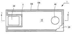
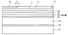
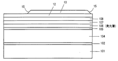
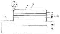
- the top view of the light emitting element of the Example Sectional drawing of the light emitting element which shows the manufacturing method of the light emitting element of the Example. Sectional drawing of the light emitting element which shows the manufacturing method of the light emitting element of the Example. Sectional drawing of the light emitting element which shows the manufacturing method of the light emitting element of the Example. Sectional drawing of the light emitting element which shows the manufacturing method of the light emitting element of the Example. Sectional drawing of the light emitting element which shows the manufacturing method of the light emitting element of the Example. Sectional drawing of the light emitting element concerning the other Example of this invention.
- an arbitrary substrate such as an insulating substrate, a conductive substrate, a non-translucent substrate, or a translucent substrate
- a substrate an arbitrary substrate such as an insulating substrate, a conductive substrate, a non-translucent substrate, or a translucent substrate
- sapphire Al 2 O 3
- silicon carbide SiC
- gallium nitride GaN
- gallium phosphide GaP
- zinc oxide ZnO
- magnesium oxide MgO
- manganese oxide MnO
- general formula Al x Ga y in 1-xy N with quaternary represented, ternary can be binary semiconductor, AlN, ceramics, or the like is used.
- the transparent conductive film examples include conductive oxide films such as metal oxides.
- conductive oxide films such as metal oxides.
- ITO indium tin oxide
- ZnO zinc oxide
- ZnO is a material (AZO, GZO) in which a few elements such as Al 2 O 3 and Ga 2 O 3 are added to ZnO, fluorine-doped zinc oxide (FTO), a composite of indium oxide and zinc oxide Niobium-doped titanium dioxide Ti 1-x Nb x O 2 (TNO), and other transparent conductive films such as zinc oxide, indium oxide, tin oxide, and cadmium (CTO) can be used.
- FTO fluorine-doped zinc oxide
- TNO titanium oxide
- CTO cadmium
- the material for the wet etching is arbitrary as long as the transparent conductive film can be etched. Also, the dry etching is optional as long as the group III nitride semiconductor can be etched, and plasma etching such as chlorine and fluorine can be used.
- the material of the first electrode and the second electrode is arbitrary, but gold, a multilayer film of gold and titanium, or an alloy of gold and titanium, a multilayer film of tungsten (W), titanium (Ti), gold (Au), etc. Nickel (Ni), titanium (Ti), gold (Au), or the like can be used.
- the method for forming the transparent conductive film can be sputtering, vacuum deposition, or the like, and is not particularly limited, but is preferably formed by vacuum deposition using an electron beam.
- the single quantum well structure and the multiple quantum well structure constituting the light emitting layer have a group III nitride compound semiconductor Al y Ga 1-yz In z N (0 ⁇ y ⁇ 1,0) containing at least indium (In). Those including a well layer of ⁇ z ⁇ 1) are desirable.
- the structure of the light emitting layer includes, for example, a well layer made of doped or undoped Ga 1-z In z N (0 ⁇ z ⁇ 1), and a group III nitride having an arbitrary composition having a larger band gap than the well layer.
- Examples thereof include a barrier layer made of a physical compound semiconductor AlGaInN.
- Preferable examples are a well layer of undoped Ga 1-z In z N (0 ⁇ z ⁇ 1) and a barrier layer made of undoped GaN.
- doping means that a dopant is intentionally included in the source gas and added to the target layer, and undoping does not intentionally add a dopant without including the dopant in the source gas. Means things. Therefore, undoped includes a case where it is naturally doped by diffusing from the adjacent layer.
- Effective methods for crystal growth of group III nitride semiconductor layers include molecular beam vapor deposition (MBE), metalorganic vapor phase epitaxy (MOVPE), hydride vapor phase epitaxy (HVPE), and liquid phase epitaxy. It is.
- the group III-V nitride semiconductor of each layer constituting the semiconductor light emitting device is at least a binary system represented by Al x Ga y InN (0 ⁇ x ⁇ 1, 0 ⁇ y ⁇ 1, 0 ⁇ x + y ⁇ 1). It can be formed of a III-V nitride compound semiconductor composed of a ternary or quaternary semiconductor.
- group III elements may be replaced by boron (B) and thallium (Tl), and part of nitrogen (N) may be phosphorus (P), arsenic (As), antimony (Sb), Bismuth (Bi) may be substituted.
- n-type impurities SiGe, Se, Te, C, etc.
- a p-type impurity is formed.
- Be, Ca, Sr, Ba, or the like can be added.
- FIG. 1 is a cross-sectional view showing a semiconductor light emitting device 1 of Example 1, and FIG. 2 is a plan view thereof.
- a buffer layer 102 made of aluminum nitride (AlN) and having a film thickness of about 20 nm is provided on a sapphire substrate 101 having a thickness of 100 ⁇ m, and a high film thickness of about 8.0 ⁇ m made of silicon (Si) -doped GaN.
- An n-type contact layer 104 (first semiconductor layer) that is a carrier concentration n + layer is formed.
- the n-type contact layer 104 has an electron concentration of 5 ⁇ 10 18 / cm 3 .
- a strain relaxation layer 105 made of In 0.03 Ga 0.97 N is formed on the n-type contact layer 104 to a thickness of 200 nm. Then, on the strain relaxation layer 105, a light emitting layer 106 having a multiple quantum well structure (MQW) formed by stacking three periods of non-doped GaN having a thickness of 20 nm and non-doped Ga 0.8 In 0.2 N having a thickness of 3 nm is formed.
- MQW multiple quantum well structure
- a p-type layer 107 corresponding to a clad layer having a film thickness of about 60 nm made of magnesium (Mg) -doped Al 0.15 Ga 0.85 N is formed on the light emitting layer 106. Further, on the p-type layer 107, a p-type contact layer 108 (second semiconductor layer) made of magnesium (Mg) -doped GaN and having a thickness of about 130 nm is formed.
- a transparent conductive film 10 made of ITO formed by MOCVD is formed on the p-type contact layer 108.
- An exposed portion 5 having a width of 3 ⁇ m is formed in the periphery of the p-type contact layer 108 on the plane.
- the width of the exposed portion 5 is preferably as narrow as possible in terms of light emission efficiency, but it is desirable to provide at least 1 ⁇ m in consideration of prevention of a short circuit of the pn junction on the side wall of the step. If it exceeds 6 ⁇ m, the luminous efficiency is lowered, so 6 ⁇ m or less is desirable.
- An insulating protective film 20 made of SiO 2 is formed on the transparent conductive film 10.
- the transparent conductive film 10 has a thickness of 0.5 ⁇ m, and the insulating protective film 20 has a thickness of 200 nm.
- the p-pad electrode 40 formed in the window opened in the insulating protective film 20 has a double structure of titanium (Ti) having a thickness of 0.01 ⁇ m and gold (Au) having a thickness of 0.5 ⁇ m. ing.
- the p electrode pad 40 may be made of an alloy of Ti and Au.
- an n-electrode 30 is formed on the n-type contact layer 104 exposed by etching from the p-type contact layer 108.
- the n electrode 30 has a double structure, and a vanadium (V) layer 31 having a thickness of about 18 nm and an aluminum (Al) layer 32 having a thickness of about 1.8 ⁇ m are partially exposed from the n-type contact layer 104. It is configured by sequentially laminating on the electrode forming portion 16 which is a part.
- the buffer layer 102 is formed on the sapphire substrate 101 by the low temperature growth of aluminum nitride (AlN) at 400 ° C. by MOCVD.
- AlN aluminum nitride
- an n-type contact layer 104 made of a group III nitride semiconductor, a strain relaxation layer 105, a light emitting layer 106, a p-type layer 107, while adjusting to the optimum temperature for epitaxial growth of each group III nitride semiconductor by MOCVD.
- the p-type contact layer 108 was laminated in order.
- Raw material gas used in the MOCVD method as the nitrogen source, ammonia (NH 3), as a Ga source, trimethyl gallium (Ga (CH 3) 3) , as an In source, trimethylindium (In (CH 3) 3) , Al source Trimethylaluminum (Al (CH 3 ) 3 ), silane (SiH 4 ) as an n-type doping gas, cyclopentadienylmagnesium (Mg (C 5 H 5 ) 2 ) as a p-type doping gas, and H as a carrier gas 2 or N 2 .
- a transparent conductive film 12 was formed by uniformly depositing ITO with a thickness of 0.5 ⁇ m on the entire surface of the p-type contact layer 108.
- a photoresist 13 was applied over the entire surface of the transparent conductive film 12 to a thickness of 4 ⁇ m. Thereafter, the photoresist 13 was exposed.
- the exposure is performed so as to incline in the direction in which the exposure intensity decreases toward the remaining region.
- the proximity exposure method changing the exposure intensity by changing the distance between the photomask and the wafer (proximity gap), or by changing the exposure intensity while keeping the proximity gap constant.
- the degree can be controlled.
- the photoresist 13 was developed, the exposed portion 80 was removed, and a photoresist 13 having an inclined portion 15 at the boundary portion 14 as shown in FIG. 4 was formed.
- the removed part corresponds to a part exposing the n-type contact layer 104.
- the transparent conductive film 12 under this portion 19 is not completely removed at the time when the etching is finished.
- the thicknesses of the photoresist 13 and the transparent conductive film 12 are designed to realize such a state.
- the exposed portion 17 of the transparent conductive film 12 was wet-etched using the remaining photoresist 13 as a mask.
- the remaining portion becomes the transparent conductive film 10 of the semiconductor light emitting device 1 shown in FIG.
- In, Sn, etc. which are constituent elements of ITO adhering to the pn junction on the side surface 18 of the step, were excluded.
- a photoresist is uniformly applied on the outermost surface, and a window is formed in the formation region of the p-pad electrode 40 on the transparent conductive film 10 by exposure and development.
- Au was deposited to a thickness of 0.5 ⁇ m, and the photoresist was lifted off to form the p-pad electrode 40.
- a photoresist is uniformly applied on the outermost surface, and a window is opened in a portion corresponding to the electrode forming portion 16 of the n-type contact layer 104 by exposure and development.
- Al was deposited to a thickness of 1.8 ⁇ m to form an n-electrode 30.
- SiO 2 is uniformly deposited on the outermost surface to a thickness of 200 nm, a photoresist is uniformly applied on the surface, and a window is opened in a predetermined region by exposure and development. Dry etching was performed with an etching gas, and then the resist was removed to form an insulating protective film 20.
- the present invention can also be used in the case of forming the flip-chip type semiconductor light emitting element 2 shown in FIG.
- the same components as those in the first embodiment are denoted by the same reference numerals.
- a first insulating protective film 20 made of SiO 2 is formed on the transparent conductive film 10, and a reflective film 50 made of Al is formed on the first insulating protective film 20.
- a second insulating protective film 21 made of SiO 2 is formed on the reflective film 50, the exposed first insulating protective film 20, and the upper surface of the element 2. That is, the 1st insulating protective film 20 and the 2nd insulating protective film 21 are united, and the reflective film 50 exists in the inside.
- a p bump electrode 70 is bonded to the p pad electrode 40, and an n bump electrode 60 is bonded to the n electrode 30.
- the electrode forming portion 16 of the n-type contact layer 104 is exposed, and the exposed portion 5 of the very small width of the p-type contact layer 108 is formed at a portion corresponding to the step edge of the electrode forming portion 16.
- the method of Example 1 can be used for etching when forming the transparent conductive film 10.
- the layer structure of the semiconductor light emitting element is arbitrary.
- a transparent conductive film is formed on a second semiconductor layer to form an electrode for the first semiconductor layer. Any method of manufacturing a light-emitting element can be applied as long as the step of etching is included.
- the present invention can be used to improve the light emission efficiency of a semiconductor light emitting device.
Landscapes
- Led Devices (AREA)
- Electrodes Of Semiconductors (AREA)
Abstract
Description
さらには、ITO膜とその上のフォトレジストをマスクとして、p型層などの半導体層を反応性ガスのプラズマを用いてドライエッチングしてn型層を露出させる場合に、ITOを構成するIn、Snなどの導電性金属原子が、pn接合の側面に付着して、リーク電流の原因となるという問題があった。
基板としては、絶縁性基板、導電性基板、不透光性基板、透光性基板など、任意の基板を用いることができる。たとえば、サファイア(Al2O3)、炭化硅素(SiC)、窒化ガリウム(GaN)、リン化ガリウム(GaP)、酸化亜鉛(ZnO)、酸化マグネシウム(MgO)、酸化マンガン(MnO)、一般式Alx Gay In1-x-y Nで表される4元、3元、2元の半導体、AlN、セラミックス、などを用いることができる。
5…露出部
10…透明導電膜
15…傾斜部
20…絶縁性保護膜
40…pパッド電極
101…サファイア基板
102…バッファ層
104…n型コンタクト層
105…歪み緩和層
106…発光層
107…p型クラッド層
108…p型コンタクト層
30…n電極
Claims (3)
- 基板と、この基板上に形成された第1伝導型の第1半導体層と、第1伝導型とは異なる第2伝導型の第2半導体層と、第2半導体層の上に形成された透明導電膜から成る第2電極と、前記第2半導体層側からエッチングして、前記第1半導体層の電極形成部を露出させ、この電極形成部に第1電極を形成する半導体発光素子の製造方法において、
前記第2半導体層上の全面に、前記透明導電膜を形成し、
形成された前記透明導電膜の上に、フォトレジストを塗布し、
前記第1半導体層の前記電極形成部の上部のフォトレジストが除去される際に、除去される部分の輪郭部において、残されたフォトレジストの厚さが除去される部分に向かって次第に薄くなるようにフォトレジストを除去し、
残されたフォトレジストをマスクとして、前記透明導電膜をウエットエッチングして、前記第2半導体層の一部を露出させ、
残された前記フォトレジスト及び前記透明導電膜をマスクとして、ドライエッチングして、前記第1半導体層の前記電極形成部を露出させ、
残された前記フォトレジストをマスクとして、前記透明導電膜の前記ドライエッチングで露出した部分をウエットエッチングし、
残されたフォトレジストを除去する
ことを特徴とする半導体発光素子の製造方法。 - 前記輪郭部におけるフォトレジストの厚さは、露光量分布を制御することにより、現像後のフォトレジストの厚さを、除去される部分に向かって次第に薄くなるように制御されることを特徴とする請求項1に記載の半導体発光素子の製造方法。
- 前記第1半導体層は、n型のIII 族窒化物半導体から成り、前記第2半導体層は、p型のIII 族窒化物半導体から成ることを特徴とする請求項1又は請求項2に記載の半導体発光素子の製造方法。
Priority Applications (2)
| Application Number | Priority Date | Filing Date | Title |
|---|---|---|---|
| US13/636,392 US8936950B2 (en) | 2010-03-23 | 2011-03-14 | Method for manufacturing semiconductor light-emitting device |
| CN201180014812.6A CN102812566B (zh) | 2010-03-23 | 2011-03-14 | 半导体发光元件制造方法 |
Applications Claiming Priority (2)
| Application Number | Priority Date | Filing Date | Title |
|---|---|---|---|
| JP2010-066087 | 2010-03-23 | ||
| JP2010066087A JP5195798B2 (ja) | 2010-03-23 | 2010-03-23 | 半導体発光素子の製造方法 |
Publications (1)
| Publication Number | Publication Date |
|---|---|
| WO2011118149A1 true WO2011118149A1 (ja) | 2011-09-29 |
Family
ID=44672730
Family Applications (1)
| Application Number | Title | Priority Date | Filing Date |
|---|---|---|---|
| PCT/JP2011/001472 Ceased WO2011118149A1 (ja) | 2010-03-23 | 2011-03-14 | 半導体発光素子の製造方法 |
Country Status (5)
| Country | Link |
|---|---|
| US (1) | US8936950B2 (ja) |
| JP (1) | JP5195798B2 (ja) |
| CN (1) | CN102812566B (ja) |
| TW (1) | TWI420698B (ja) |
| WO (1) | WO2011118149A1 (ja) |
Cited By (1)
| Publication number | Priority date | Publication date | Assignee | Title |
|---|---|---|---|---|
| EP2744931A4 (en) * | 2011-08-18 | 2015-01-21 | Affinity Biosciences Pty Ltd | SOLUBLE POLYPEPTIDE |
Families Citing this family (13)
| Publication number | Priority date | Publication date | Assignee | Title |
|---|---|---|---|---|
| KR101883842B1 (ko) | 2011-12-26 | 2018-08-01 | 엘지이노텍 주식회사 | 발광소자 및 이를 포함하는 조명시스템 |
| WO2014014298A1 (ko) | 2012-07-18 | 2014-01-23 | 주식회사 세미콘라이트 | 반도체 발광소자의 제조 방법 |
| EP2782148B1 (en) | 2012-07-18 | 2020-05-06 | Semicon Light Co. Ltd. | Semiconductor light-emitting device |
| CN108493308A (zh) | 2012-07-18 | 2018-09-04 | 世迈克琉明有限公司 | 半导体发光器件 |
| DE102013107971A1 (de) * | 2013-07-25 | 2015-01-29 | Osram Opto Semiconductors Gmbh | Optoelektronischer Halbleiterchip, Halbleiterbauelement und Verfahren zur Herstellung von optoelektronischen Halbleiterchips |
| TW201513397A (zh) * | 2013-09-26 | 2015-04-01 | Lextar Electronics Corp | 發光二極體之製造方法 |
| DE102014107555A1 (de) * | 2014-05-28 | 2015-12-03 | Osram Opto Semiconductors Gmbh | Elektrische Kontaktstruktur für ein Halbleiterbauelement und Halbleiterbauelement |
| CN104659169A (zh) * | 2015-02-15 | 2015-05-27 | 映瑞光电科技(上海)有限公司 | 一种简易倒装led及其制作方法 |
| CN106410007B (zh) * | 2016-09-22 | 2019-07-19 | 佛山市国星半导体技术有限公司 | 一种双层电极led芯片及其制作方法 |
| CN108511574A (zh) * | 2017-02-28 | 2018-09-07 | 山东浪潮华光光电子股份有限公司 | 一种GaN基发光二极管芯片的制备方法 |
| CN111063771A (zh) * | 2020-01-06 | 2020-04-24 | 江西圆融光电科技有限公司 | Led芯片的制备方法及led芯片 |
| CN116417546A (zh) * | 2021-12-31 | 2023-07-11 | 厦门市三安光电科技有限公司 | 微发光二极管及其制备方法、发光装置 |
| JP2024039386A (ja) | 2022-09-09 | 2024-03-22 | 日亜化学工業株式会社 | 発光素子の製造方法 |
Citations (5)
| Publication number | Priority date | Publication date | Assignee | Title |
|---|---|---|---|---|
| JPH07130701A (ja) * | 1993-11-05 | 1995-05-19 | Fuji Electric Co Ltd | 透明導電膜のパターニング方法 |
| JP2001185758A (ja) * | 2000-10-25 | 2001-07-06 | Toyoda Gosei Co Ltd | 3族窒化物化合物半導体発光素子 |
| JP2005268725A (ja) * | 2004-03-22 | 2005-09-29 | Sony Corp | 半導体素子およびその製造方法 |
| JP2006049829A (ja) * | 2004-06-29 | 2006-02-16 | Fuji Xerox Co Ltd | 表面発光型半導体レーザおよびその製造方法 |
| JP2006339384A (ja) * | 2005-06-01 | 2006-12-14 | Kyocera Corp | 発光素子およびその製造方法ならびにその発光素子を用いた照明装置 |
Family Cites Families (9)
| Publication number | Priority date | Publication date | Assignee | Title |
|---|---|---|---|---|
| JPH10173229A (ja) | 1996-12-09 | 1998-06-26 | Toyoda Gosei Co Ltd | 3族窒化物半導体発光素子の製造方法 |
| TW595014B (en) * | 2002-12-05 | 2004-06-21 | Inst Nuclear Energy Res Aec | Manufacturing method of LED |
| KR100593886B1 (ko) | 2003-06-24 | 2006-07-03 | 삼성전기주식회사 | 질화갈륨계 반도체 발광소자의 제조방법 |
| US7033949B2 (en) * | 2003-12-29 | 2006-04-25 | Formosa Epitaxy Incorporation | Structure and manufacturing method for nitride-based light-emitting diodes |
| US7352787B2 (en) * | 2004-06-29 | 2008-04-01 | Fuji Xerox Co., Ltd. | Vertical cavity surface emitting laser diode and process for producing the same |
| TWI250671B (en) * | 2005-03-01 | 2006-03-01 | Epitech Technology Corp | Method for manufacturing light-emitting diode |
| KR100652864B1 (ko) * | 2005-12-16 | 2006-12-04 | 서울옵토디바이스주식회사 | 개선된 투명전극 구조체를 갖는 교류용 발광 다이오드 |
| TWI355096B (en) * | 2006-12-29 | 2011-12-21 | Epistar Corp | Light-emitting diode structure and method for manu |
| KR100980649B1 (ko) * | 2008-05-20 | 2010-09-08 | 고려대학교 산학협력단 | 굴곡이 형성된 반사층을 포함하는 발광소자 및 그 제조방법 |
-
2010
- 2010-03-23 JP JP2010066087A patent/JP5195798B2/ja active Active
-
2011
- 2011-03-14 US US13/636,392 patent/US8936950B2/en active Active
- 2011-03-14 WO PCT/JP2011/001472 patent/WO2011118149A1/ja not_active Ceased
- 2011-03-14 CN CN201180014812.6A patent/CN102812566B/zh active Active
- 2011-03-18 TW TW100109399A patent/TWI420698B/zh active
Patent Citations (5)
| Publication number | Priority date | Publication date | Assignee | Title |
|---|---|---|---|---|
| JPH07130701A (ja) * | 1993-11-05 | 1995-05-19 | Fuji Electric Co Ltd | 透明導電膜のパターニング方法 |
| JP2001185758A (ja) * | 2000-10-25 | 2001-07-06 | Toyoda Gosei Co Ltd | 3族窒化物化合物半導体発光素子 |
| JP2005268725A (ja) * | 2004-03-22 | 2005-09-29 | Sony Corp | 半導体素子およびその製造方法 |
| JP2006049829A (ja) * | 2004-06-29 | 2006-02-16 | Fuji Xerox Co Ltd | 表面発光型半導体レーザおよびその製造方法 |
| JP2006339384A (ja) * | 2005-06-01 | 2006-12-14 | Kyocera Corp | 発光素子およびその製造方法ならびにその発光素子を用いた照明装置 |
Cited By (2)
| Publication number | Priority date | Publication date | Assignee | Title |
|---|---|---|---|---|
| EP2744931A4 (en) * | 2011-08-18 | 2015-01-21 | Affinity Biosciences Pty Ltd | SOLUBLE POLYPEPTIDE |
| US10087261B2 (en) | 2011-08-18 | 2018-10-02 | Affinity Biosciences Pty Ltd | Soluble polypeptides |
Also Published As
| Publication number | Publication date |
|---|---|
| US20130011953A1 (en) | 2013-01-10 |
| CN102812566A (zh) | 2012-12-05 |
| TWI420698B (zh) | 2013-12-21 |
| TW201205857A (en) | 2012-02-01 |
| JP2011199122A (ja) | 2011-10-06 |
| JP5195798B2 (ja) | 2013-05-15 |
| CN102812566B (zh) | 2015-05-06 |
| US8936950B2 (en) | 2015-01-20 |
Similar Documents
| Publication | Publication Date | Title |
|---|---|---|
| JP5195798B2 (ja) | 半導体発光素子の製造方法 | |
| JP4123828B2 (ja) | 半導体発光素子 | |
| CN102201515B (zh) | 半导体发光器件 | |
| CN113875030B (zh) | 包括钝化层的发光二极管前体 | |
| KR101537330B1 (ko) | 질화물 반도체 발광 소자 제조 방법 | |
| JP2005277374A (ja) | Iii族窒化物系化合物半導体発光素子及びその製造方法 | |
| KR100833313B1 (ko) | 질화갈륨계 발광다이오드 소자 및 그의 제조방법 | |
| JP2008294188A (ja) | 半導体発光素子及びその製造方法 | |
| JP4699258B2 (ja) | フリップチップ発光ダイオード及びその製造方法 | |
| KR100609118B1 (ko) | 플립 칩 발광다이오드 및 그 제조방법 | |
| CN111403565A (zh) | 发光二极管及其制作方法 | |
| JP5353809B2 (ja) | 半導体発光素子及び発光装置 | |
| JP4292925B2 (ja) | Iii族窒化物系化合物半導体発光素子の製造方法 | |
| JP4853198B2 (ja) | Iii族窒化物系化合物半導体発光素子 | |
| KR20110139909A (ko) | 질화물 반도체 발광소자의 제조방법 및 이에 의해 제조된 질화물 반도체 발광소자 | |
| WO2010038740A1 (ja) | 半導体発光素子の製造方法 | |
| JP5900400B2 (ja) | Iii族窒化物半導体発光素子の製造方法 | |
| KR100738399B1 (ko) | 질화물 반도체 발광소자 | |
| JP5434343B2 (ja) | Ito電極の形成方法、半導体素子のito電極及びito電極を備えた半導体素子 | |
| JP2011159801A (ja) | 半導体発光素子及びその製造方法、並びにランプ | |
| US8541772B2 (en) | Nitride semiconductor stacked structure and method for manufacturing same and nitride semiconductor device | |
| KR20090112854A (ko) | 그룹 3족 질화물계 반도체 발광다이오드 소자 및 이의 제조방법 | |
| JP2004356442A (ja) | Iii族窒化物系化合物半導体発光素子 | |
| CN107078189A (zh) | 半导体发光组件 | |
| KR20090115830A (ko) | 수직구조의 그룹 3족 질화물계 반도체 발광다이오드 소자및 제조방법 |
Legal Events
| Date | Code | Title | Description |
|---|---|---|---|
| WWE | Wipo information: entry into national phase |
Ref document number: 201180014812.6 Country of ref document: CN |
|
| 121 | Ep: the epo has been informed by wipo that ep was designated in this application |
Ref document number: 11758961 Country of ref document: EP Kind code of ref document: A1 |
|
| WWE | Wipo information: entry into national phase |
Ref document number: 13636392 Country of ref document: US |
|
| NENP | Non-entry into the national phase |
Ref country code: DE |
|
| 122 | Ep: pct application non-entry in european phase |
Ref document number: 11758961 Country of ref document: EP Kind code of ref document: A1 |