WO2011104969A1 - 窒化物半導体多重量子障壁を有する発光素子及びその製造方法 - Google Patents
窒化物半導体多重量子障壁を有する発光素子及びその製造方法 Download PDFInfo
- Publication number
- WO2011104969A1 WO2011104969A1 PCT/JP2010/071524 JP2010071524W WO2011104969A1 WO 2011104969 A1 WO2011104969 A1 WO 2011104969A1 JP 2010071524 W JP2010071524 W JP 2010071524W WO 2011104969 A1 WO2011104969 A1 WO 2011104969A1
- Authority
- WO
- WIPO (PCT)
- Prior art keywords
- layer
- barrier
- layers
- pair
- mqb
- Prior art date
- Legal status (The legal status is an assumption and is not a legal conclusion. Google has not performed a legal analysis and makes no representation as to the accuracy of the status listed.)
- Ceased
Links
Images


Classifications
-
- H—ELECTRICITY
- H10—SEMICONDUCTOR DEVICES; ELECTRIC SOLID-STATE DEVICES NOT OTHERWISE PROVIDED FOR
- H10H—INORGANIC LIGHT-EMITTING SEMICONDUCTOR DEVICES HAVING POTENTIAL BARRIERS
- H10H20/00—Individual inorganic light-emitting semiconductor devices having potential barriers, e.g. light-emitting diodes [LED]
- H10H20/80—Constructional details
- H10H20/81—Bodies
- H10H20/811—Bodies having quantum effect structures or superlattices, e.g. tunnel junctions
-
- H—ELECTRICITY
- H10—SEMICONDUCTOR DEVICES; ELECTRIC SOLID-STATE DEVICES NOT OTHERWISE PROVIDED FOR
- H10H—INORGANIC LIGHT-EMITTING SEMICONDUCTOR DEVICES HAVING POTENTIAL BARRIERS
- H10H20/00—Individual inorganic light-emitting semiconductor devices having potential barriers, e.g. light-emitting diodes [LED]
- H10H20/80—Constructional details
- H10H20/81—Bodies
-
- H—ELECTRICITY
- H10—SEMICONDUCTOR DEVICES; ELECTRIC SOLID-STATE DEVICES NOT OTHERWISE PROVIDED FOR
- H10H—INORGANIC LIGHT-EMITTING SEMICONDUCTOR DEVICES HAVING POTENTIAL BARRIERS
- H10H20/00—Individual inorganic light-emitting semiconductor devices having potential barriers, e.g. light-emitting diodes [LED]
- H10H20/80—Constructional details
- H10H20/81—Bodies
- H10H20/811—Bodies having quantum effect structures or superlattices, e.g. tunnel junctions
- H10H20/812—Bodies having quantum effect structures or superlattices, e.g. tunnel junctions within the light-emitting regions, e.g. having quantum confinement structures
-
- H—ELECTRICITY
- H10—SEMICONDUCTOR DEVICES; ELECTRIC SOLID-STATE DEVICES NOT OTHERWISE PROVIDED FOR
- H10H—INORGANIC LIGHT-EMITTING SEMICONDUCTOR DEVICES HAVING POTENTIAL BARRIERS
- H10H20/00—Individual inorganic light-emitting semiconductor devices having potential barriers, e.g. light-emitting diodes [LED]
- H10H20/80—Constructional details
- H10H20/81—Bodies
- H10H20/815—Bodies having stress relaxation structures, e.g. buffer layers
-
- H—ELECTRICITY
- H10—SEMICONDUCTOR DEVICES; ELECTRIC SOLID-STATE DEVICES NOT OTHERWISE PROVIDED FOR
- H10H—INORGANIC LIGHT-EMITTING SEMICONDUCTOR DEVICES HAVING POTENTIAL BARRIERS
- H10H20/00—Individual inorganic light-emitting semiconductor devices having potential barriers, e.g. light-emitting diodes [LED]
- H10H20/80—Constructional details
- H10H20/81—Bodies
- H10H20/822—Materials of the light-emitting regions
- H10H20/824—Materials of the light-emitting regions comprising only Group III-V materials, e.g. GaP
- H10H20/825—Materials of the light-emitting regions comprising only Group III-V materials, e.g. GaP containing nitrogen, e.g. GaN
Definitions
- the present invention relates to a nitride semiconductor light emitting device technology, and more particularly to a high efficiency technology such as an AlGaN deep ultraviolet light emitting device using a multiple quantum barrier (MQB).
- MQB multiple quantum barrier
- Nitride semiconductors such as AlN, GaN, and InN are direct transition type semiconductors.
- the composition is appropriately set and the band gap is changed to change the depth from the infrared. It has a feature that it can emit light up to ultraviolet. In particular, the ultraviolet region is an undeveloped region, and future research and development is expected.
- LEDs / LDs Semiconductor deep ultraviolet light sources having a wavelength of 220 to 350 nm are expected to be widely realized in the future for sterilization / water purification, medical field, biochemical industry, and the like.
- light source for high-density optical recording, white illumination, industrial application to UV curable resin, various sensing such as fluorescence analysis, environmental destruction substances (dioxin, environmental hormone, PCB, etc.) by combination with titanium oxide There is a wide range of applications due to high-speed decomposition processing. It is known that the bactericidal effect is most effective at a wavelength in the vicinity of 260 to 280 nm, which overlaps with the absorption wavelength of DNA.
- the band gap energy of the AlGaN-based material ranges from 3.4 eV of GaN to 6.2 eV of AlN, and covers the ultraviolet light emitting region of various gas lasers conventionally used.
- AlGaN-based ultraviolet light-emitting devices have progressed with 15 years of development so far, but at present, the efficiency is still about 1%, which is currently lower than that of blue LEDs (80% or more). .
- the reduction of threading dislocation density in the AlN underlayer was the key to realizing an ultraviolet LED.
- a reduction in dislocation density of about 1/100 compared to the conventional one has been realized, and as a result, in the conventional 220-320 nm band AlGaN, 0.5% is achieved.
- the internal quantum efficiency which was less than or equal to 50%, was enhanced to about 50%.
- the efficiency of electron injection into the light emitting layer is still as low as about 10-30%.
- the light extraction efficiency of the ultraviolet LED is as low as 6-8% due to ultraviolet light absorption in the vicinity of the contact layer / electrode.
- the external quantum efficiency of the ultraviolet LED determined by the combination of these is as low as about 1% and should be improved by future research.
- electron injection efficiency it has been considered impossible to realize high electron injection efficiency for a long time because of the physical limitations that the hole concentration of p-type AlGaN cannot be improved.
- the external quantum efficiency of 220-360 nm band AlGaN or InAlGaN-based deep ultraviolet LEDs is still lower than that of blue LEDs (80% or more).
- the external quantum efficiency is currently about 7% at 340-350 nm, about 1% at 260-280 nm, and about 0.1-0.5% at 230-250 nm.
- the external quantum efficiency (EQE: External Quantum Efficiency) of the ultraviolet LED is expressed by the following equation.
- the ultraviolet emission IQE of the AlGaN quantum well is dramatically improved to about 50%, and about 80% by adding about 0.3% In to AlGaN. IQE is obtained.
- EIE Electron Injection Efficiency
- LOE Light Extraction Efficiency
- the low light extraction efficiency is caused by the ultraviolet light absorption near the contact layer electrode and the low light reflectivity of the p-type electrode. In the future, the electrode reflectivity will be improved, the Al reflector, and the two-dimensional photonic crystal structure. It is thought that it will be improved by the introduction of.
- the low electron injection efficiency is caused by the low hole concentration of p-type AlGaN, and is determined by the physical property value that the Mg acceptor level of AlGaN is deep, so that improvement is difficult.
- the hole concentration in AlGaN is 10 16 cm ⁇ 3 or less when the Al composition is 50 to 70%, and 10 14 cm ⁇ 3 or less when the Al composition is 70 to 90%, and is 5 ⁇ 10 5 used in a normal pn junction element. Remarkably low compared to about 17 cm ⁇ 3 . For this reason, in the AlGaN ultraviolet LED, electrons are not injected into the light emitting region, but leak into the p-side layer, thereby reducing the electron injection efficiency. The electron injection efficiency was improved to some extent by using the electron blocking layer.
- An object of the present invention is to provide an elemental technique for further increasing the emission intensity of deep ultraviolet light while using an AlGaInN-based material, particularly an AlGaN-based material, as a material for a light-emitting layer.
- a method is proposed in which a multiple quantum barrier is used in the electron blocking layer to achieve an effect that exceeds the physical property limit, and the efficiency of the nitride ultraviolet light-emitting device is dramatically improved.
- a barrier height several times higher than the electron barrier height determined by the band gap in the bulk crystal can be realized. If this effect is used, the electron injection efficiency, which has been 10-30% until now, can be increased to 80-100%. Using this method, it is conventionally caused by the low hole concentration of the p-type semiconductor.
- the LD uses an injection current density of about 10 to 100 times that of the LED during operation, so that the electron injection efficiency (EIE) is expected to be further reduced to about 1/10. Therefore, it is considered extremely difficult to realize a 250-330 nm band ultraviolet LD with a low hole concentration and an insufficient electron barrier height.
- Wavelength 250-330 nm band ultraviolet LD has not been realized yet because of the above-mentioned difficulties.
- the electron injection efficiency of 10% or less predicted by the ultraviolet LD is improved to 50-100%, and the realization of a wavelength 250-330 nm band ultraviolet LD becomes possible for the first time. It is considered to be.
- the influence of nitride semiconductor multiple quantum barriers on improving the efficiency of ultraviolet light emitting devices is immense.
- the application fields of ultraviolet semiconductor light-emitting devices are expected to expand dramatically.
- x Al y Ga 1-xy N (0 ⁇ x ⁇ 0.1, 0 ⁇ y ⁇ 1) layer and In x 1Al y 1Ga 1-x1-y1 N (on the n-type InAlGaN layer) 0 ⁇ x1 ⁇ 0.5,0 ⁇ y1 ⁇ 1) quantum well layers and Inx2Al y 2Ga 1-x2-y2 N (0 ⁇ x2 ⁇ 0.3,0 ⁇ y2 ⁇ 1, x1> x2, y1 ⁇ y2) Quantum well light-emitting layer comprising a barrier layer, and p-type In x Al y Ga 1-xy N (0 ⁇ x ⁇ 0.1, 0 ⁇ y ⁇ 1) layer formed on the InAlGaN quantum well light-emitting layer And a multiple quantum barrier electron blocking layer formed on the p-type InAlGaN layer.
- Nitride semiconductor ultraviolet light-emitting device that emits light in ⁇ 390 nm.
- the multi-quantum barrier electron blocking layer formed on the p-type InAlGaN layer is composed of In x1 Al y1 Ga 1-x1-y1 N (0 ⁇ x1 ⁇ 0.1, 0 ⁇ y1 ⁇ 1) barrier layer and In x2.
- a plurality of pairs of Al y2 Ga 1-x2-y2 N (0 ⁇ x2 ⁇ 0.3, 0 ⁇ y2 ⁇ 1, x1 ⁇ x2, y1> y2) valley layers are formed, and the first pair of layers
- the two pairs of layers are separated from each other, and the layer thickness of the first pair of layers is greater than the layer thickness of the second pair of layers, or the layer thickness of the first pair of layers Is thinner than the second pair of layers, and from the quantum well light emitting layer side toward the opposite side of the substrate, the first pair of layers and the second pair It is preferred that the pairs of layers are provided in that order. The above description will be described with reference to FIG. 11, for example.
- “In x1 Al y1 Ga 1-x1-y1 N (0 ⁇ x1 ⁇ 0.1, 0 ⁇ y1 ⁇ 1) barrier layer and In x2 Al y2 Ga 1 ⁇ x2 ⁇ y2N (0 ⁇ x2 ⁇ 0.3, 0 ⁇ y2 ⁇ 1, x1 ⁇ x2, y1> y2) pair with the valley layer ” means, for example, 2ML and 2ML barrier layers and valleys in MQB.
- Each pair with a layer is meant. That is, in this case, it means that the pair is formed by 8 periods.
- the second pair of layers has a layer thickness different from that of the first pair of layers, for example, the first pair of layers is the one of 2ML / 2ML in FIG.
- 11 3ML / 3ML means that both are formed spatially separated.
- the thickness of the first pair is thinner than the thickness of the second pair of layers, and the side opposite to the substrate from the quantum well light emitting layer side.
- the first pair of layers and the second pair of layers are provided in that order toward the direction, whereas in FIG. 11B, the layer thickness of the first pair of layers. Is thicker than the layer thickness of the second pair of layers, and the first pair of layers and the second pair of layers from the quantum well light emitting layer side toward the opposite side of the substrate. It shows that the layers are provided in that order.
- the multi-quantum barrier electron blocking layer formed on the p-type InAlGaN layer is composed of In x 1Al y1 Ga 1-x1-y1 N (0 ⁇ x1 ⁇ 0.1, 0 ⁇ y1 ⁇ 1) barrier layer and In x2.
- a plurality of pairs with the valley layer are formed, the first pair of layers, The second pair of layers and the third pair of layers are separated from each other, and the layer thickness of the first pair of layers is greater than the layer thickness of the second pair of layers;
- the layer thickness of the pair is thicker than that of the third pair of layers, or the layer thickness of the first pair of layers is thinner than the layer thickness of the second pair of layers,
- the first, second, and second layers are thinner than the third pair of layers and from the quantum well light emitting layer side toward the opposite side of the substrate. It is preferable that the pair of layers is provided in that order.
- the above description basically means that, in addition to the first pair of layers and the second pair of layers, for example, a third pair of layers of 4ML / 4ML is provided.
- the 3ML / 3ML second pair and the 4ML / 4ML third pair may be adjacent to each other or may be separated from each other. “Separated” here refers to the case of being separated.
- the pairs of layers having different thicknesses describe the first to fourth examples, the first pair of layers, the second pair of layers, and the third pair of layers May not be said to be provided apart from each other. In practice, the case where more types of pairs of layers than the example shown in FIG.
- the barrier layer and the barrier layer in the pair of layers may have the same number of molecular layers. This description indicates that, as shown in FIG. 11, for example, two cycles of 2ML and 2ML may be provided, and the layers may have the same number of molecular layers.
- the nitride semiconductor ultraviolet light emitting element is preferably a light emitting diode.
- the multiple quantum barrier electron blocking layer In x 1Al y1 Ga 1-x1-y1 N (0 ⁇ x1 ⁇ 0.1,0 ⁇ y1 ⁇ 1) barrier layer and In x2 Al y2 Ga 1-x2-y2 N ( 0 ⁇ x2 ⁇ 0.3, 0 ⁇ y2 ⁇ 1, x1 ⁇ x2, y1> y2) Layers having the same period, or layers having a second period different from the first period and the first period And a multi-quantum barrier electron blocking layer stacked in multiple layers.
- the present invention also near ultraviolet with MQB, purple, blue, as a green light emitting element, a AlxGa1-xN (0 ⁇ x ⁇ 1) buffer layer formed on the substrate, the Al x Ga 1-x N buffer N-type In x Al y Ga 1-xy N (0 ⁇ x ⁇ 0.1, 0 ⁇ y ⁇ 1) layer formed on the layer and In x1 Al formed on the n-type InAlGaN layer y1 Ga 1-x1-y1 N (0 ⁇ x1 ⁇ 0.5,0 ⁇ y1 ⁇ 1) quantum well layers and the In x2 Al y2 Ga 1-x2 -y2 N (0 ⁇ x2 ⁇ 0.3,0 ⁇ y2 ⁇ 1, x1> x2, y1 ⁇ y2) Quantum well light-emitting layer including a barrier layer, and p-type In x Al y Ga 1-xy N (0 ⁇ x ⁇ ) formed on the InAlGaN quantum well light-emitting layer.
- a near-ultraviolet, violet, blue, and green nitride semiconductor light-emitting element that emits light at a wavelength of 390 to 550 nm and has an electron blocking layer may be used.
- the nitride semiconductor light emitting device is characterized in that the period increases or decreases sequentially from the active layer side toward the multiple quantum barrier electron blocking layer side.
- the multiple quantum barrier electron blocking layer is a nonpolar layer formed on the A plane or M plane, or a layer formed on a semipolar plane.
- the A plane and the M plane are well-known polar planes.
- the electron blocking effect is enhanced as compared with the case of a single barrier.
- the higher the barrier height and the longer the MQB period the better the electron blocking effect.
- MQB and changing its period in order electrons can be blocked over a wide energy range, and the electron blocking effect is more remarkable than MQB having the same period.
- FIG. 1A is a perspective view showing one configuration example of an AlGaN and InAlGaN ultraviolet LED (250 nm band) using a multiple quantum well barrier according to an embodiment of the present invention.
- FIG. 1B is a perspective view showing a configuration example of an AlGaN and InAlGaN ultraviolet LED (280 nm band) using a multiple quantum well barrier according to an embodiment of the present invention.
- FIG. 2 is a diagram illustrating an example of an LED structure having an AlGaN / AlN buffer layer structure.
- FIG. 3 is a diagram schematically showing an advantage of a multiple quantum barrier compared to a general single electron block layer.
- FIG. 4 is a diagram showing room temperature operation light emission characteristics of an AlGaN ultraviolet LED (wavelength 250 to 262 nm) using multiple quantum barriers.
- FIG. 5 shows the efficiency improvement of the AlGaN ultraviolet LED by the multiple quantum barrier at a wavelength of 250 nm.
- FIG. 6 is a diagram showing the operating characteristics of a 262 nm AlGaN ultraviolet LED using multiple quantum barriers.
- FIG. 7 is a diagram showing the effect (wavelength dependence) of improving the external quantum effect by the multiple quantum barrier.
- FIG. 8 is an energy band structure showing one configuration example of an MQW type LED using MQB according to an embodiment of the present invention, and is a diagram showing an end of a conduction band of a nonpolar LED grown on the A plane.
- FIG. 8 is an energy band structure showing one configuration example of an MQW type LED using MQB according to an embodiment of the present invention, and is a diagram showing an end of a conduction band of a nonpolar LED grown on the A plane.
- FIG. 10A shows the electrons in a non-polar LED grown on the A-plane of the higher barrier corresponding to FIG. 8 (a) for well thickness / barrier thickness from 2 ML to 15 ML and for a single barrier of 20 nm. It is a figure which shows the energy dependence of the transmittance
- FIG. 10B shows electrons for a non-polar LED grown on the A-plane of the higher barrier corresponding to FIG. 8 (a) for well / barrier thicknesses from 2 ML to 15 ML and for a single barrier of 20 nm. It is a figure which shows the energy dependence of the transmittance
- FIG. 10B shows the electrons for a non-polar LED grown on the A-plane of the higher barrier corresponding to FIG. 8 (a) for well / barrier thicknesses from 2 ML to 15 ML and for a single barrier of 20 nm. It is a figure which shows the energy dependence of the transmittance
- FIG. 11 is a diagram showing the energy dependency of the electron transmittance when a single barrier and MQB are used based on the result of FIG.
- FIG. 12 is a diagram showing the dependence on the total thickness of the MQB layer with different periods regarding the energy dependence of the electron transmittance in the case of MQB having no polarity grown on the A plane.
- FIG. 13A is a diagram showing the energy dependence of the electron transmittance in the case of MQB having no polarity grown on the A-plane of the lower barrier corresponding to FIG.
- FIG. 13B is a diagram showing the energy dependence of the electron transmittance in the case of MQB having no polarity grown on the A-plane of the lower barrier corresponding to FIG.
- FIG. 13A is a diagram showing the energy dependence of the electron transmittance in the case of MQB having no polarity grown on the A-plane of the lower barrier corresponding to FIG.
- FIG. 13B is a diagram showing the energy dependence of the electron transmittance in
- FIG. 14 is a diagram showing the dependence of the electron transmittance on the energy dependence of the MQB layer with a different period on the energy dependence of the electron transmittance in the case of a nonpolar MQB grown on the A-plane (FIG. 13). is there.
- FIG. 15 is a diagram showing the electron transmittance dependency of energy for each period when growing on the A-plane (no polarity) when the barrier is high and when the barrier is low.
- FIG. 16 is a diagram showing the relationship between the MQB period and the electron transmittance with the barrier height as a parameter according to the present embodiment.
- FIG. 17A is a diagram showing characteristics in the case of MQB grown on the C-plane instead of the A-plane, which is almost the same as the first embodiment.
- FIG. 17A is a diagram showing characteristics in the case of MQB grown on the C-plane instead of the A-plane, which is almost the same as the first embodiment.
- FIG. 17B is a diagram showing characteristics in the case of MQB grown on the C-plane instead of the A-plane, which is almost the same as the first embodiment.
- FIG. 18 is a diagram showing characteristics in the case of MQB grown on the C-plane instead of the A-plane, which is almost the same as the first embodiment.
- FIG. 19A is a diagram showing the characteristics in the case of MQB grown on the C-plane instead of the A-plane, although it is almost the same as the first embodiment.
- FIG. 19B is a diagram showing characteristics in the case of MQB grown on the C-plane instead of the A-plane, which is almost the same as the first embodiment.
- FIG. 20 is a diagram showing characteristics in the case of MQB grown on the C-plane instead of the A-plane, although it is almost the same as the first embodiment.
- Multi-quantum barrier electron blocking layer (MQB) comprising 5 layers each of Al 0.95 Ga 0.05 N (4 nm) / Al 0.77 Ga 0.23 N (2 nm), 17... P-Al 0.77 Ga 0.23 N layer, 21 ... Mg doped p-GaN contact layer, 23 ... Ni / Au n-type electrode, 25 ... Ni / Au p-type electrode, 27 ... UV output.
- FIG. 1A is a perspective view showing one configuration example of an AlGaN ultraviolet LED using a multiple quantum well barrier according to an embodiment of the present invention.
- a 250 nm ultraviolet LED (A) is formed on a sapphire substrate 1 and has a multiple AlN buffer layer 3 with reduced threading dislocations and an n-Al 0.77 Ga 0.23 N; Si buffer layer.
- MQW multiple quantum well light emitting layer 7
- MQW multiple quantum well light emitting layer 7
- MQW multiple quantum well light emitting layer 7
- Mg-doped Multiple layers composed of p-Al 0.77 Ga 0.23 N layer 11 (25 nm) and five layers of Al 0.95 Ga 0.05 N (4 nm) / Al 0.77 Ga 0.23 N (2 nm).
- FIG. 1B is a perspective view showing a configuration example of an InAlGaN ultraviolet LED using a multiple quantum well barrier according to an embodiment of the present invention. As shown in FIG.
- the 280 nm ultraviolet LED is formed on the sapphire substrate 1 and has an i-AlN regrowth layer (0.2 ⁇ m) 3a and a multiple Al 0.7 Ga 0.3 N buffer with reduced threading dislocations.
- FIG. 2 is a diagram illustrating an example of a buffer portion of an LED structure having an AlGaN / AlN buffer layer structure.
- the ultraviolet emission internal quantum efficiency (IQE) of the AlGaN quantum well is 0.5% or less. Therefore, in order to realize a nitride semiconductor ultraviolet light emitting element, it is particularly required to use an AlGaN buffer having a low threading dislocation density.
- the threading dislocation density is about 1 ⁇ 10 9 cm ⁇ 2
- the IQE of the AlGaN quantum well is about 30%.
- the resulting manufacturing method is essential.
- the method presented in FIG. 2 is a method for producing an AlN buffer on a sapphire substrate using the “ammonia pulse supply multi-stage growth method”, and was proposed as a method that satisfies all of the above 1) to 4).
- AlN nucleation 3a is performed on the sapphire substrate 1 by an ammonia pulse supply method (left figure), followed by nucleation embedding 3b (pulse supply) by lateral enhancement growth, followed by flattening by vertical high-speed growth. And crack prevention (continuous supply) 3c, and further flattening (pulse supply / continuous supply: right figure) growth 3d for preventing threading dislocations by repetition.
- an AlN high quality buffer layer can be realized by the NH 3 pulse supply multi-stage growth method, and threading dislocation can be reduced, and crack free and surface flattening can be achieved.
- the chart (a) in the upper left is a diagram showing an ammonia pulse flow of TMAl and NH 3 .
- an AlN-based material is grown by supplying TMAl and NH 3 by MOCVD (organic metal CVD).
- MOCVD organic metal CVD
- MOCVD organic metal CVD
- Table 1 shows an example of crystal growth conditions in MOCVD growth of each layer having a 250 nm band AlGaN structure having MQB.
- the growth layer AlN1 is a nucleation layer
- AlN2 is a buried layer
- AlN3 is a continuous growth layer
- AlGaN1 is a barrier layer
- AlGaN2 is an MQB barrier layer.
- Examples of the growth conditions of MOCVD used in Table 1 are the nucleation layer (3a) of the AMN buffer formed by “ammonia pulse supply multistage growth method” (ammonia pulse growth: growth condition AlN1), the pulse growth buried layer (3b) (ammonia Pulse growth: growth condition AlN2), continuous growth AlN (3c) (growth condition AlN3), and barrier layer (growth condition AlGaN1) and MQB barrier layer (growth condition AlGaN2) of a 250 nm band AlGaN quantum well LED are shown.
- the ultraviolet (deep ultraviolet) light emitting element will be described.
- Table 2 is a diagram showing the Al composition of each AlGaN layer, the external quantum efficiency (EQE ultraviolet) of the LED, and the value of the ultraviolet light output in the 249 nm band, 250 nm band, and 262 nm band.
- the maximum value of EQE is 1.50%, and the maximum output is 8.7 mW.
- the maximum value of EQE is 1.15% and the maximum output is 15.0 mW.
- the maximum value of EQE is 1.54% and the maximum output is 10.4 mW, and such a high value is obtained.
- Examples of the growth conditions of MOCVD used in Table 1 above are the “ammonia pulse supply multistage growth method” formation AlN buffer nucleation layer (3a) (ammonia pulse growth: growth condition AlN1), pulse growth buried layer (3b) (Ammonia pulse growth: growth condition AlN2), continuous growth AlN (3c) (growth condition AlN3), and barrier layer (growth condition AlGaN1) and MQB barrier layer (growth condition AlGaN2) of 250 nm band AlGaN quantum well LED .
- As conditions for growing the AlN buffer in order to improve the quality of the AlN crystal, a temperature (1200-1300 ° C.) higher than the growth temperature (1000-1120 ° C.) generally used for GaN or AlGaN is used.
- the V / III ratio (molar ratio between the supply amount of the group V element and the supply amount of the group III element) is also lower than the value generally used for GaN or AlGaN (2000 or more).
- the general growth conditions for AlGaN are used.
- FIG. 3 is a diagram schematically showing an advantage of a multiple quantum barrier compared to a general single electron block layer.
- the figure shows the profile of the Al composition of the 250 nm band AlGaN quantum well LED. At the same time, it is considered that the tendency is almost the same as the band profile during LED operation in the case of a nonpolar crystal. Therefore, it is a figure useful for generally explaining the effect of MQB.
- the band profile in a crystal having a strong polarity grown on the C-plane needs to consider the inclination of the band as shown in FIG. 9 described later, and is somewhat complicated to understand.
- FIG. 3B in the case of a single barrier with respect to electrons of Al 0.95 Ga 0.05 N: Mg (25 nm), electrons having energy below the height can be reflected almost completely. However, the electrons higher than the barrier can hardly be reflected. Therefore, the electron barrier height is limited by the band discontinuity value of the conduction band. As shown in FIG.
- the limit of the electron block height is determined by the material constituting the SQB, whereas in the MQB, in addition to the material limit, the barrier height is increased by a quantum mechanical multilayer reflection effect. It is possible to further increase the thickness. As will be described later, the effective barrier height can be improved up to about 3.5 times by optimizing the barrier height and thickness of each layer.
- the electron injection efficiency of the AlGaN ultraviolet LED is 10-30% (240-280 nm). This is a low hindrance to the band LED, and has been a major obstacle to increasing the efficiency of ultraviolet LEDs. In addition, this low electron injection efficiency is attributed to the low hole concentration of p-type AlGaN, and has not been solved. If MQB formed by the design guideline proposed by the present invention is used, the above problem is considered to be fundamentally solved, and the MQB effect is extremely important in realizing an AlGaN-based high-efficiency ultraviolet LED.
- the electron leakage to the p-side layer increases with a spur due to an increase in carrier density in the light emitting layer region that occurs with an increase in injection current density.
- the injection current density of the ultraviolet LD is about 10 to 100 times that of the ultraviolet LED, the electron injection efficiency is further reduced, and it is considered that the current density does not reach the oscillation threshold value and is destroyed by overheating. Even if it oscillates, it is impossible to obtain a high output.
- MQB is characterized by realizing a high electron block height, so it has a great effect on reflecting high energy electrons due to an increase in carrier density, and it makes ultraviolet LD oscillation and high efficiency.
- FIG. 4 is a diagram showing room-temperature operating light emission characteristics of an AlGaN quantum well ultraviolet LED (wavelength 250-262 nm) using multiple quantum barriers. As shown in FIG.
- FIG. 5 is an example showing the efficiency improvement of an AlGaN quantum well ultraviolet LED by an electron block layer using a multiple quantum barrier at a wavelength of 250 nm. For comparison, the characteristics of a single electron block layer (EBL) are shown.
- FIG. 5A shows the ultraviolet light output
- FIG. 5B shows the EQE (external quantum efficiency).
- FIG. 6 is a diagram showing the operating characteristics of a 262 nm AlGaN ultraviolet LED using multiple quantum barriers. As shown in FIG. 6, it was possible to obtain good characteristics of EQE of 1.54% and output power of 10.4 mW. Table 2 summarizes the EQE and output of the near-wavelength AlGaN quantum well ultraviolet LEDs obtained at this stage. The Al composition of each AlGaN layer is also shown. At a wavelength of 249 nm, the maximum EQE value is 1.5% and the maximum output is 8.7 mW.
- the maximum value of EQE is 1.54% and the maximum output is 10.4 mW.
- a continuous output of 15.0 mW at 250 nm is obtained.
- FIG. 7 is a diagram showing the effect (wavelength dependence) of improving the external quantum effect by using a multiple quantum barrier (MQB) electron block layer. It can be seen that a larger external quantum efficiency can be obtained when an electron blocking layer with multiple quantum barriers is used than when an electron blocking layer with a single barrier is used. Large values are obtained even at room temperature. Here, a remarkable effect is obtained in the 250 nm to 260 nm band.
- the highest EQE value (1.5% at 249 nm) of the AlGaN quantum well LED using MQB was found to be about a 4-fold improvement over 0.4% using conventional SQB.
- the maximum output (15.0 mW at 250 nm) was about 7 times that at 2.2 nm compared to 2.2 mW when the conventional SQB was used.
- the efficiency and output can be further improved.
- the same effect can be obtained in a wide ultraviolet region from 220 nm to 390 nm.
- ⁇ ext is the external quantum efficiency (EQE)
- ⁇ int is the internal quantum efficiency (IQE)
- ⁇ ext is the light extraction efficiency (LEE)
- ⁇ inj is the electron injection efficiency (EIE).
- IQE is estimated to be about 30% from the temperature dependence of photoluminescence (PL) emission of a sample having the same structure.
- the LEE is calculated from the element structure and is estimated to be about 6%.
- EIE electron injection efficiency
- the same LED having a single electron block layer has an EQE of 0.4%, and IQE and LEE are almost at the same level, so the EIE is estimated to be 22%. Therefore, the electron injection efficiency has increased from 22% to about 83% due to the introduction of MQB, and the effect is enormous. From this result, it can be seen that the problem of reduced electron injection efficiency due to the low hole concentration of p-type AlGaN can be almost solved by introducing MQB.
- FIG. 8 is an energy band structure showing one configuration example of an MQW type LED using MQB according to an embodiment of the present invention, and is a diagram showing an end of a conduction band of a nonpolar LED grown on the A plane.
- the Al composition is 50% / 70% / 95% for each of well / barrier / MQB (when the barrier height is high), as shown in FIG. 8B.
- the Al composition is 75% / 85% / 95% of well / barrier / MQB (when the barrier height is low), respectively.
- 8 and 9 show energy band diagrams in an operating state in which a voltage is applied between the electrodes. Electrons reflected by the MQB fall into the MQW and improve the light emission efficiency.
- the band profile during operation of the LED without polarity has a slight inclination to transport electrons and holes, it can be replaced with a substantially flat band structure as shown in FIG. This can be used to explain the general effect.
- FIG. 8A assumes a 270 nm band AlGaN quantum well LED, and assumes that the MQB barrier height is as large as about 0.6 eV.
- FIGS. 9C and 9D are LED layer structures similar to those shown in FIGS. 8A and 8B, but are examples in which crystals grow on the C plane and have a strong polarity.
- a crystal structure of a wurtzite structure (hexagonal crystal) is generally used, and growth on a C plane where high quality crystals are easily obtained in crystal growth is often used.
- FIG. 9D shows a band profile when a 230 nm band LED is identified and the difference between the barrier composition and the valley composition of AlGaN constituting the MQB is as small as 10%.
- the band inclination due to polarization is about half, but the influence on the MQB effect and quantum well confinement is still large.
- MQB is characterized by using a quantum mechanical electron multiple reflection effect. As shown in FIG. 10, it can be seen that the shorter the period between the barrier and the well, the more the electron reflection region is formed in the high energy band due to the quantum mechanical effect. When a thicker barrier (for example, 7 ML or more) is used, a plurality of reflection band bands are generated.
- the reflected energy band is 1.7-2.2 eV, 0.8-1.2 eV, 0.55-0 in the barrier / valley MQB of 2ML, 3ML, 4ML, 5ML, 7ML, 10ML, 15ML, for example. .9 eV, 0.35-0.75 eV, 0.65 eV or less, 0.8-1.0 eV, 0.75 eV or less, 0.7 eV or less.
- a transmission band with high transmittance is formed in an energy band lower than the reflection band.
- the transmission band band is 0.3-1.7 eV, 0.3-0.85 eV, 0.25-0.55 eV, 0.25-0 in 3ML, 4ML, 5ML, and 7ML barrier / valley MQB, for example. .35 eV, 0.65-0.8 eV. Therefore, it can be seen that this structure is difficult to use. In a structure actually used, it is important not to generate an electron transmission band, and it is necessary to configure a combination of a plurality of periods of barriers / wells.
- a major feature of the nitride semiconductor MQB is that the barrier thickness expected to be effective is very thin, such as 2 ML to 10 ML.
- FIG. 11A and 11B are diagrams showing the energy dependency of the electron transmittance when a single barrier and MQB are used based on the result of FIG. Several barrier periods are used in combination so that high electron reflection is obtained over as much energy as possible than the energy at the band edge of the barrier.
- FIG. 11A is a diagram showing an MQB showing an example of a structure in which the barrier period increases in order from the MQW side
- FIG. 11B shows an example in which the order of the periods is reversed.
- FIG. In any case, the energy dependency of the electron transmittance is low over a wide range as compared with the example shown in FIG. 10, and it is understood that the utility as an electron blocking layer is high.
- the effective barrier height is about 3.5 times higher than that of the single barrier.
- FIGS. 12 is a diagram showing the dependence on the total thickness of the MQB layer with different periods regarding the energy dependence of the electron transmittance in the case of MQB having no polarity grown on the A plane. It can be seen that the larger the total thickness, the more the electrons are reflected to a higher energy value. This shows that as the number of types of MQBs increases, the reflection of electrons occurs in a large energy range, so that the effect of reflection of electrons increases. From the figure, it can be seen that even when the total thickness of MQB is as small as 20 nm, the effective barrier height by MQB is about twice that of a single barrier, and a large reflection effect can be obtained even with a thin total thickness of MQB. . FIGS.
- FIG. 13A (a) to 13B (h) show the energy dependence of the electron transmittance in the case of MQB having no polarity grown on the A-plane of the lower barrier corresponding to FIG. 8 (a).
- FIG. 11 when a higher barrier (FIG. 11) is used, the relationship between the period and the reflected energy band is almost the same, but the reflected energy band becomes narrower. Moreover, the reflectance of electrons becomes low. Therefore, when MQB having a low barrier is used, a design such as increasing the number of periods of the barrier is required.
- FIG. 14 is a diagram showing the dependence of the electron transmittance on the energy dependence of the MQB layer with a different period on the energy dependence of the electron transmittance in the case of a nonpolar MQB grown on the A-plane (FIG. 13). is there. It can be seen that the larger the total thickness, the more the electrons are reflected to a higher energy value. However, compared to the case of FIG. 12, electrons can be reflected only to a lower energy. As shown in FIGS. 14B and 14C, the larger the total thickness of the layer, the more the electrons can be reflected up to a higher energy.
- the effective barrier height is In the case of 3 times and a total thickness of about 25 nm, about 2 times is obtained. Since a sufficient effective height can be obtained even with a total thickness of 25 nm, it has been found that a large MQB effect can be obtained even when a barrier height as low as about 10% is used with an Al composition difference.
- a design that realizes a high reflectance without forming a transmission band in a wide energy band is somewhat complicated. Therefore, it is necessary to show a guideline indicating how many layers of barriers should be combined.
- FIG. 15A and 15B are diagrams showing the electron transmittance dependency of energy for each period when growing on the A-plane (no polarity) when the barrier is high and when the barrier is low. .
- the higher the barrier the more the electrons can be reflected in a wide energy range.
- the shorter the period the higher the electron transmittance, that is, the longer the period, the more electrons can be blocked.
- FIG. 16 is a diagram showing the relationship between the MQB period and the electron transmittance with the barrier height as a parameter according to the present embodiment. As shown in FIG.
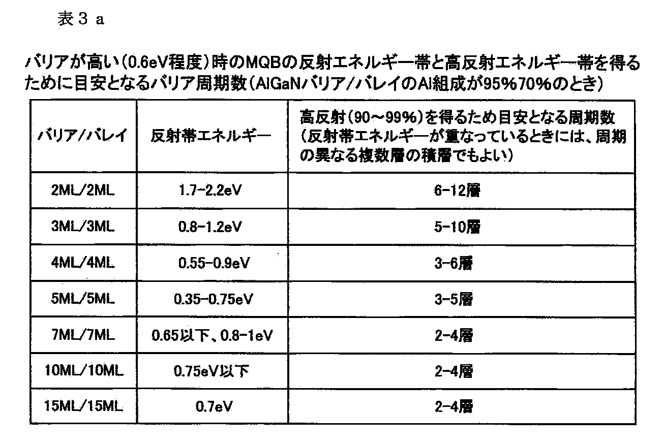
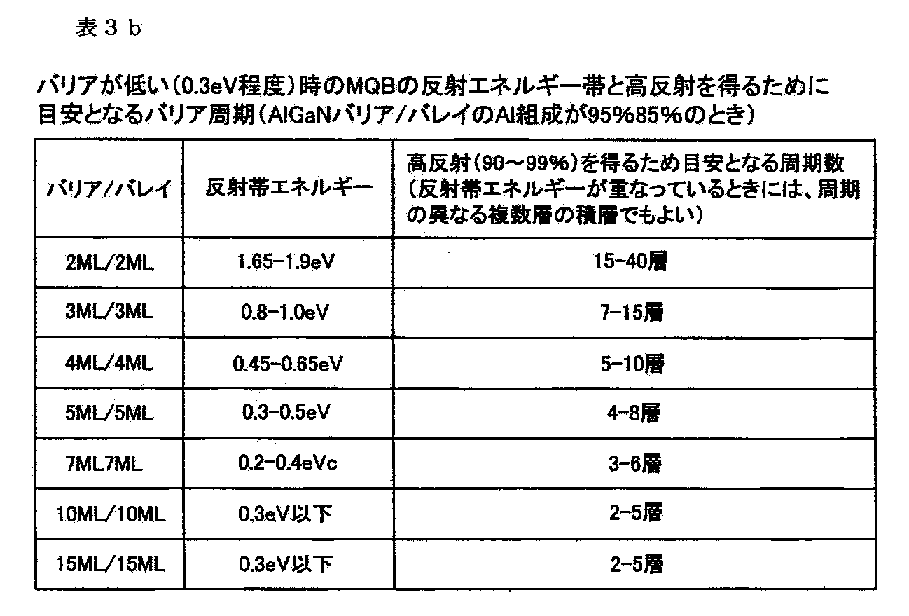
- Table 3 summarizes the values of the reflection energy band in which high reflection can be obtained and the number of barrier periods as a guide. As a measure of the period at which high reflection is obtained, the number of periods at which a reflectance of 90-99% is obtained is shown.
- Table 3 (a) shows a barrier height as high as about 0.6 eV (when the Al composition of the barrier / valley AlGaN is 95% / 70%), and Table 3 (b) shows a barrier height of 0. A low time of about 3 eV was assumed (when the Al composition of the barrier / valley AlGaN was 95% / 85%).
- FIGS. 17A to 20 are diagrams showing the characteristics in the case of MQB grown on the C-plane instead of the A-plane, which is almost the same as the first embodiment.
- the tendency of the MQB effect when there is polarity is basically the same as the effect when there is no polarity, but it is somewhat complicated such that the reflectance is blurred due to the influence of the band inclination.
- the barrier energy becomes a sawtooth shape even in the case of a single barrier, so that an electron barrier that is originally higher than when there is no polarity is formed. Therefore, the increase in effective barrier height due to MQB is smaller than when there is no polarity.
- FIG. 17 shows the MQB total thickness dependence of the MQB effect when the barrier is high.
- the effective barrier height is about twice that of a single barrier, and when the MQB total thickness is 30 nm, it is about 1.5 times, and a large effective barrier even when there is polarity on the normal C-plane. It can be seen that the height can be secured.
- FIG. 19 is an analysis example of the reflectance when the barrier is low similarly. The influence of polarization is reduced compared to the case where the Al composition ratio is large, but the reflectance broadening effect due to polarization cannot be ignored.
- FIG. 20 shows the MQB total thickness dependence of the MQB effect when the barrier is low.
- the effective barrier height is about 1.3 times that of a single barrier, and when the total MQB thickness is 55 nm, about 1.5 times is obtained, and when the overall MQB thickness is small.
- the electron blocking effect is better than in the case of a single barrier. From these results, it can be seen that even in the case of a polar crystal grown on the C-plane, a large increase in effective barrier height similar to that in the case of no polarity can be obtained.
- the ultraviolet light-emitting device has been described as an example.
- the multiple quantum barrier structure according to the present invention can also be used for nitride semiconductor light-emitting devices having other light emission wavelengths.
- the effect of MQB is considered to be very useful in the near-ultraviolet and green light-emitting elements, and is very important in improving the efficiency of nitride light-emitting elements in a wide wavelength range of wavelengths 220 to 550 nm.
- the use of MQB increases the electron blocking effect compared to the case of a single barrier. Further, it can be seen that the electron blocking effect is improved as the barrier height is higher and the period of MQB is longer in both the case of growing on the A plane and the case of the polar crystal grown on the C plane. .
- the electron injection efficiency of the AlGaN ultraviolet LED is 10-30% (240-280 nm). This is a low hindrance to the band LED, and has been a major obstacle to increasing the efficiency of ultraviolet LEDs. In addition, this low electron injection efficiency is attributed to the low hole concentration of p-type AlGaN, and has not been solved. If MQB formed by the design guideline proposed in this patent is used, the above problem is considered to be fundamentally solved, and the MQB effect is extremely important in realizing an AlGaN-based high-efficiency ultraviolet LED.
- the electron leakage to the p-side layer increases with a spur due to an increase in carrier density in the light emitting layer region that occurs with an increase in injection current density. Since the injection current density of the ultraviolet LD is about 10 to 100 times that of the ultraviolet LED, the electron injection efficiency is further reduced, and it is considered that the current density does not reach the oscillation threshold value and is destroyed by overheating. Even if it oscillates, it is impossible to obtain a high output. As mentioned above, MQB is characterized by realizing a high electron block height, so it has a great effect on reflecting high energy electrons due to an increase in carrier density, and it makes ultraviolet LD oscillation and high efficiency.
- MQB metal-oxide-semiconductor
- a barrier layer having a low Al composition of 10% or less an effective electron block height several times that of the barrier layer can be realized, and the maximum effect can be obtained with a low Al composition. I can do it. Therefore, it is possible to improve the droop while realizing low resistance p-type layer conduction and low distortion of each layer.
- the use of MQB improves the efficiency at the time of high current injection, enables stable high-power operation of the blue LED, and is highly important.
- the effect of MQB is considered to be very useful also in the near-ultraviolet and green light-emitting elements, and is very important in increasing the efficiency of nitride light-emitting elements in a wide wavelength range of wavelengths 220 to 550 nm.
- the present invention can be used for an ultraviolet LED / LD composed of a nitride semiconductor and a near ultraviolet, purple, blue, and green LED / LD. All publications, patents and patent applications cited herein are incorporated herein by reference in their entirety.
Landscapes
- Led Devices (AREA)
- Semiconductor Lasers (AREA)
Abstract
Description
波長220~350nmの半導体深紫外光源(LED・LD)は、今後、殺菌・浄水、医療分野・生化学産業などへの幅広い応用が考えられ、その実現が期待されている。さらにその他にも、高密度光記録用光源や白色照明、紫外硬化樹脂等への産業応用、蛍光分析などの各種センシング、酸化チタンとの組み合わせによる環境破壊物質(ダイオキシン、環境ホルモン、PCB等)の高速分解処理などがあり応用範囲は幅広い。殺菌効果では、DNAの吸収波長と重なる260−280nm付近の波長で最も効果が高いことが知られている。半導体紫外光源は、今後高効率化が進むにつれ市場規模は飛躍的に大きくなってくると考えられ、高効率・高出力の紫外LED・LDの開発は重要な課題である。
これまでの紫外光源としては、エキシマレーザやアルゴンイオンSHGレーザ、エキシマランプなどのガス固体紫外光源に限られており、それらは大型で寿命も短くまた高価であったため一般への応用は難しかったが、それらを置き換える半導体紫外LED、LDが実現すれば、ガス固体光源に比べ超小型、高効率、高出力、長寿命、低コスト紫外光源となり、幅広い応用分野が開けると考えられる。応用分野から要求が大きいことから、特に窒化物AlGaN系深紫外光源開発は今後の重要性が高い。
紫外発光素子を実現する材料の選択において、AlGaN系材料のバンドギャップエネルギーはGaNの3.4eVからAlNの6.2eVにわたり、従来用いられてきた各種ガスレーザーの紫外発光領域をカバーしている。それに加え、1)全組成領域において直接遷移型半導体である、2)量子井戸からの紫外高効率発光が可能である、3)p・n型半導体の形成が可能である、4)材料が堅く素子寿命が長い、5)砒素、水銀、鉛などの有害な材料を含まず環境に安全である、等の特徴を持つ。これらの理由により、実用可能な紫外発光素子を実現するための材料としてAlGaN系材料は最も有力である。
これまでの15年程度の開発により、AlGaN系紫外発光デバイスは進展してきたが、現在のところ、まだ効率は1%程度であり、青色LED(80%以上)等に比べ低いのが現状である。AlN下地層の貫通転位密度の低減が紫外LEDを実現する要であったが、近年、従来に比べ1/100程度の転位密度低減が実現され、それにより従来220−320nm帯AlGaNにおいて0.5%以下であった内部量子効率が50%程度に増強された。さらにInをAlGaNに混入することによりさらに80%程度まで改善されている(例えば、特許文献1参照)。
しかし、AlGaNのp型濃度が依然低いことに起因し、電子の発光層への注入効率は依然として10−30%程度と低い。また、紫外LEDの光取り出し効率はコンタクト層・電極付近の紫外光吸収などのため、6−8%と低い。これらのかけあわせで決まる紫外LEDの外部量子効率は1%程度と低く、今後の研究により改善されるべきものである。
特に、電子注入効率に関しては、p型AlGaNのホール濃度を改善できないという物性的な限界ゆえに、長い間、高い電子注入効率を実現することが不可能であると考えられてきた。今回、多重量子障壁電子ブロック層をAlGaN、もしくはInAlGaN系紫外LEDに導入し、電子の注入効率を10−30%から推定80%以上に向上させることに実験的に成功し、「p型AlGaNの不可能」に起因する電子注入の問題を根本から解決する方法を提案・実証した。本明細書の内容は、窒化物紫外発光素子の電子注入効率を向上させるための、多重量子障壁電子ブロック層の導入に関するもので、その設計指針と実際の導入の効果解析値、及び実際の深紫外LEDへの実施と世界最高出力値の実現について示すものである。
ηext=ηint(内部量子効率)×ηlee(光取り出し効率)×ηinj(電子注入効率)
これまでの研究開発によりAlGaN系量子井戸の紫外発光の内部量子効率(IQE:Internal Quantum Efficiency)は格段に向上し、最近80%以上のIQEが実現している。AlGaNは青色LEDで用いられるInGaN材料と異なり、貫通転位の存在により発光効率が著しく減少してしまうため、従来までの貫通転位密度の高いAlNバッファー層を用いた場合では、0.5%以下の低いIQEしか得られなかった。しかし、AlNバッファー層の貫通転位密度の低減によりAlGaN系量子井戸の紫外発光IQEは飛躍的に向上し50%程度が実現され、さらにAlGaNに0.3%程度のInを加えることにより80%程度のIQEが得られている。これらの開発により、AlGaN系紫外発光素子の内部量子効率の問題はすでに解決されてきた。
しかしながら、依然として、電子の発光層への注入効率(EIE:Electron Injection Efficiency)は10−30%、紫外LEDの光取り出し効率(LEE:Light Extraction Efficiency)は6−8%と低い。これらのかけあわせで決まる紫外LEDの外部量子効率は1%程度と低く、今後の研究により改善される必要がある。
低い光取り出し効率(LEE)は、コンタクト層電極付近の紫外光吸収およびp型電極の低い光反射率に起因しており、今後、電極反射率の向上、Al反射板、2次元フォトニック結晶構造の導入などにより改善されていくと考えられる。
一方、低い電子注入効率(EIE)はp型AlGaNの低いホール濃度に起因しており、AlGaNのMgアクセプターのレベルが深いという物性値によって決まっているため、改善は難しい。AlGaN中のホール濃度は、Al組成が50−70%では1016cm−3以下、Al組成が70−90%では1014cm−3以下であり、通常のpn接合素子で用いられる5×1017cm−3程度に比べ著しく低い。そのため、AlGaN紫外LEDでは、電子は発光領域注入されずに、p側層にリークしてしまい、電子注入効率を低下させる。電子ブロック層を用いることにより電子注入効率はある程度改善された。しかし、最も電子バリアを高くするため、バンドギャップの大きいAlNあるいはAl組成95%以上のAlGaNを電子ブロック層の材料に選択しているが、いまだ十分な電子注入効率は得られていない。電子注入効率(EIE)の値は、260−280nm帯AlGaN量子井戸LEDで推定30%程度、240−260nm帯LEDで推定10−30%、220−240nm帯LEDで10%以下と考えられる。
本発明は、発光層の材料としてAlGaInN系の材料、特に、AlGaN系の材料を用いつつ、深紫外光の発光強度をさらに高めるための要素技術を提供することを目的とする。
量子力学的な電子の多重反射効果を用いると、バルク結晶のときのバンドギャップで決まる電子バリア高さよりも、さらに、数倍高いバリア高さを実現することが出来る。この効果を使えば、これまで10−30%であった電子注入効率は、80−100%に向上させることが可能である、この方法を使い、従来、p型半導体の低ホール濃度に起因して解決が難しかった電子注入効率の問題を根本から解決することが出来る。
本方法をもちいれば、AlGaN、InAlGaN系紫外LEDの効率を飛躍的に向上させることが可能である。また、今後開発が予定されている、AlGaN系紫外LDの実現において大きな効果を発揮すると考えられる。上記の電子注入効率は注入電流密度が高くなるに従い、その低下が激しくなる。特にLDでは動作時に、LEDに比べて10−100倍程度の注入電流密度を用いるため、電子注入効率(EIE)はさらに1/10程度に低減されると予測される。したがって、ホール濃度が低く、また電子バリア高さが十分でない、250−330nm帯紫外LDの実現はきわめて困難であると考えられる。波長250−330nm帯紫外LDは上記の困難の故にまだ実現されていない。
しかし、本発明の窒化物半導体多重量子障壁を用いれば、紫外LDで予測される10%以下の電子注入効率は50−100%に向上され、波長250−330nm帯紫外LDの実現が初めて可能になると考えられる。
上記のように、窒化物半導体多重量子障壁の紫外発光素子効率改善への影響は計り知れなく大きい。また、窒化物半導体多重量子障壁を用いて高効率動作を実現した220−390nm帯紫外高効率LED、ならびに紫外LDの出現により、紫外半導体発光素子の応用分野は飛躍的に広がると考えられる。
同様のMQBの効果は、波長390−550nmの近紫外、紫、青、緑発光LD、LEDにも応用可能であり、大きな効果が期待できる。特に青色LEDなどで問題となっている高出力動作時の効率の低下(ドゥループ)を大きく改善する方法として重要性が高い。
本発明の一観点によれば、基板に形成されたAlxGa1−xN(0<x<1)バッファ層と、前記AlxGa1−xNバッファ層上に形成されたn型InxAlyGa1−x−yN(0<x<0.1,0<y<1)層と、前記n型InAlGaN層上に形成されたInx1Aly1Ga1−x1−y1N(0<x1<0.5,0<y1<1)量子井戸層とInx2Aly2Ga1−x2−y2N(0<x2<0.3,0<y2<1,x1>x2,y1<y2)バリア層からなる量子井戸発光層と、前記InAlGaN量子井戸発光層上に形成されたp型InxAlyGa1−x−yN(0<x<0.1,0<y<1)層と、前記p型InAlGaN層上に形成された多重量子障壁電子ブロック層と、を備えた波長220~390nmで発光する窒化物半導体紫外発光素子が提供される。
また、p型InAlGaN層上に形成された多重量子障壁電子ブロック層は、Inx1Aly1Ga1−x1−y1N(0<x1<0.1,0<y1<1)バリア層とInx2Aly2Ga1−x2−y2N(0<x2<0.3,0<y2<1,x1<x2,y1>y2)バレイ層との対が複数形成され、第1の対の層と第2の対の層はそれぞれ離れており、前記第1の対の層の層厚の方が前記第2の対の層の層厚より厚いか、或いは、前記第1の対の層の層厚の方が前記第2の対の層の層厚より薄く、かつ、前記量子井戸発光層側の側から前記基板と反対側の方に向かって、前記第1の対の層と前記第2の対の層がその順番で設けられていることが好ましい。
上記の記載を例えば図11を参照して説明すると、「Inx1Aly1Ga1−x1−y1N(0<x1<0.1,0<y1<1)バリア層とInx2Aly2Ga1−x2−y2N(0<x2<0.3,0<y2<1,x1<x2,y1>y2)バレイ層との対」とは、MQBにおいて、例えば、2MLと2MLのバリア層とバレイ層とのそれぞれの1対を意味している。すなわち、この場合は、対が8周期だけ形成されていることを意味している。
また、第2の対の層とは、第1の対の層とは層厚の異なる、例えば、第1の対の層を図11の2ML/2MLのもの、第2の対の層を図11の3ML/3MLのものとすると、その両者は空間的に離されて形成されていることを意味する。
このMQBでは、図11(a)では、第1の対の層厚の方が前記第2の対の層の層厚より薄く、かつ、前記量子井戸発光層側の側から前記基板と反対側の方に向かって、前記第1の対の層と前記第2の対の層とがその順番で設けられており、一方、図11(b)では、前記第1の対の層の層厚の方が前記第2の対の層の層厚より厚く、前記量子井戸発光層側の側から前記基板と反対側の方に向かって、前記第1の対の層と前記第2の対の層がその順番で設けられていることを示している。
また、p型InAlGaN層上に形成された多重量子障壁電子ブロック層は、Inx1Aly1Ga1−x1−y1N(0<x1<0.1,0<y1<1)バリア層とInx2Aly2Ga1−x2−y2N(0<x2<0.3,0<y2<1,x1<x2,y1>y2)バレイ層との対が複数形成され、第1の対の層、第2の対の層および第3の対の層はそれぞれ離れており、前記第1の対の層の層厚の方が前記第2の対の層の層厚より厚く、前記第2の層の対の層厚が前記第3の対の層より厚いか、或いは、前記第1の対の層の層厚の方が前記第2の対の層の層厚より薄く、前記第2の層の対の層厚が前記第3の対の層より薄く、かつ、前記量子井戸発光層側の側から前記基板と反対側の方に向かって、前記第1、第2および第3の層の対がその順番で設けられていることが好ましい。
上記の記載については、基本的に、上記第1の対の層と第2の対の層の他に、例えば4ML/4MLの第3の対の層が設けられていることを意味している。
ここで、3ML/3MLの第2の対と4ML/4MLの第3の対とは、隣接している場合もあるが、離れている場合もある。ここでいう「離れており」とは、このうちの離れている場合を述べている。
また、図11では、厚さの異なる対の層が第1から第4までの例を記載しているため、第1の対の層と第2の対の層と第3の対の層とがそれぞれ離れて設けられていると言えない場合もあり得る。実際には、図11で示す例よりもより多くの種類の対の層、例えば5種類以上の異なる厚さの対の層が設けられている場合も本発明の実施例の範疇に入る。そのような場合には、第1の対の層と第2の対の層と第3の対の層とをそれぞれ離れていると言うことができる。
前記対の層における前記バリア層と前記バレイ層とが同じ分子層数であっても良い。この記載は、図11に示すように、例えば、2MLと2MLの層が8周期設けられているというように、同じ分子層数の層であるようにしても良いことを示している。
また、上記窒化物半導体紫外発光素子は、発光ダイオードであることが好ましい。
前記多重量子障壁電子ブロック層として、Inx1Aly1Ga1−x1−y1N(0<x1<0.1,0<y1<1)バリア層とInx2Aly2Ga1−x2−y2N(0<x2<0.3,0<y2<1,x1<x2,y1>y2)バレイ層を、同一周期、または、第1の周期及び前記第1の周期とは異なる第2の周期の層で多層積層した多重量子障壁電子ブロック層を有することを特徴とする。
また、本発明は、MQBを用いた近紫外、紫、青、緑色発光素子として、基板に形成されたAlxGa1−xN(0<x<1)バッファ層と、前記AlxGa1−xNバッファ層上に形成されたn型InxAlyGa1−x−yN(0<x<0.1,0<y<1)層と、前記n型InAlGaN層上に形成されたInx1Aly1Ga1−x1−y1N(0<x1<0.5,0<y1<1)量子井戸層とInx2Aly2Ga1−x2−y2N(0<x2<0.3,0<y2<1,x1>x2,y1<y2)バリア層からなる量子井戸発光層と、前記InAlGaN量子井戸発光層上に形成されたp型InxAlyGa1−x−yN(0<x<0.1,0<y<1)層と、前記p型InAlGaN層上に形成された多重量子障壁電子ブロック層と、を備え、前記多重量子障壁電子ブロック層として、Inx1Aly1Ga1−x1−y1N(0<x1<0.1,0<y1<1)バリア層とInx2Aly2Ga1−x2−y2N(0<x2<0.3,0<y2<1,x1<x2,y1>y2)バレイ層を、同一周期、または、異なる周期で多層積層した多重量子障壁電子ブロック層を有することを特徴とする、波長390~550nmで発光する、近紫外、紫、青、緑色窒化物半導体発光素子であっても良い。
前記窒化物半導体発光素子は、前記活性層側から前記多重量子障壁電子ブロック層側に向けて、前記周期が、順次大きくなるか或いは順次小さくなることを特徴とする。
また、無極性の場合、すなわち、前記多重量子障壁電子ブロック層は、A面,M面上に形成された極性の無い層、あるいは半極性面に形成された層であることを特徴とする。窒化物半導体では、A面、M面はよく知られた極性面である。
本発明の他の観点によれば、III族窒化物単結晶上に形成する発光素子構造の成長方法において、基板上にAlxGa1−xN(0<x<1)バッファ層を成長するステップと、前記AlxGa1−xNバッファ層上にn型InxAlyGa1−x−yN(0<x<0.1,0<y<1)層を成長するステップと、前記n型InAlGaN層上にInx1Aly1Ga1−x1−y1N(0<x1<0.5,0<y1<1)量子井戸層とInx2Aly2Ga1−x2−y2N(0<x2<0.3,0<y2<1,x1>x2,y1<y2)バリア層からなる量子井戸発光層を成長するステップと、前記InAlGaN発光層上にp型InxAlyGa1−x−yN(0<x<0.1,0<y<1)層を成長するステップと、前記p型InAlGaN層上にInx1Aly1Ga1−x1−y1N(0<x1<0.1,0<y1<1)バリア層とInx2Aly2Ga1−x2−y2N(0<x2<0.1,0<y2<1,x1<x2,y1>y2)バレイ層を多層積層した多重量子障壁電子ブロック層を成長するステップと、を有することを特徴とする発光素子構造の成長方法が提供される。
本明細書は本願の優先権の基礎である日本国特許出願2010−038912号の明細書および/または図面に記載される内容を包含する。
さらに、MQBを用い、その周期を順番に変化させることにより、広いエネルギー範囲にわたって、電子をブロックすることができ、同じ周期のMQBに比べてより電子ブロック効果が顕著である。
図1Bは、本発明の実施の形態による多重量子井戸障壁を用いたAlGaN及びInAlGaN紫外LED(280nm帯)の一構成例を示す斜視図である。
図2は、AlGaN/AlNバッファー層の構造を備えたLED構造の一例を示す図である。
図3は、多重量子障壁について一般的な単一電子ブロック層と比べた利点を模式的に示した図面である。
図4は、多重量子障壁を用いたAlGaN紫外LED(波長250−262nm)の室温動作発光特性を示す図である。
図5は、多重量子障壁によるAlGaN紫外LEDの効率向上を波長250nmにおいて示したものである。
図6は、多重量子障壁を用いた262nmAlGaN紫外LEDの動作特性を示す図である。
図7は、多重量子障壁による外部量子効果向上の効果(波長依存性)を示す図である。
図8は、本発明の実施例によるMQBを利用したMQW型LEDの一構成例を示すエネルギーバンド構造であり、A面上に成長した極性のないLEDの伝導帯の端を示す図である。
図9は、C面上に成長させる(極性あり)場合の例である。
図10Aは、図8(a)に対応する高めのバリアのA面上に成長した極性のないLEDにおいて、2MLから15MLまでの井戸厚/バリア厚の場合と、20nmのシングルバリアの場合の電子の透過率のエネルギー依存性を示す図である。
図10Bは、図8(a)に対応する高めのバリアのA面上に成長した極性のないLEDにおいて、2MLから15MLまでの井戸厚/バリア厚の場合と、20nmのシングルバリアの場合の電子の透過率のエネルギー依存性を示す図である。
図11は、図10の結果に基づいて、単一バリアとMQBとを用いた場合の、電子の透過率のエネルギー依存性を示す図である。
図12は、A面上に成長した極性のないMQBの場合における、電子の透過率のエネルギー依存に関する、周期を異ならせたMQB層の総厚依存性を示す図である。
図13Aは、図8(a)に対応する低めのバリアのA面上に成長した極性のないMQBの場合における、電子の透過率のエネルギー依存性を示す図である。
図13Bは、図8(a)に対応する低めのバリアのA面上に成長した極性のないMQBの場合における、電子の透過率のエネルギー依存性を示す図である。
図14は、A面上に成長した極性のないMQB(低いバリア;図13)の場合における、電子の透過率のエネルギー依存に関する、周期を異ならせたMQB層の総厚依存性を示す図である。
図15は、バリアが高い時とバリアが低い時における、A面上に成長(極性なし)した場合における、周期別のエネルギーの電子透過率依存性を示す図である。
図16は、本実施例によるバリア高さをパラメータとしたMQBの周期と電子の透過率との関係を示す図である。
図17Aは、上記第1の実施の形態とほぼ同じであるが、A面ではなくC面に成長したMQBの場合の特性を示す図である。
図17Bは、上記第1の実施の形態とほぼ同じであるが、A面ではなくC面に成長したMQBの場合の特性を示す図である。
図18は、上記第1の実施の形態とほぼ同じであるが、A面ではなくC面に成長したMQBの場合の特性を示す図である。
図19Aは、上記第1の実施の形態とほぼ同じであるが、A面ではなくC面に成長したMQBの場合の特性を示す図である。
図19Bは、上記第1の実施の形態とほぼ同じであるが、A面ではなくC面に成長したMQBの場合の特性を示す図である。
図20は、上記第1の実施の形態とほぼ同じであるが、A面ではなくC面に成長したMQBの場合の特性を示す図である。
図1Bは、本発明の実施の形態による多重量子井戸障壁を用いたInAlGaN紫外LEDの一構成例を示す斜視図である。図1Bに示すように、280nm紫外LEDは、サファイア基板1上に形成され、i−AlN再成長層(0.2μm)3aと、貫通転位を低減した多重Al0.7Ga0.3Nバッファー層5aと、n−In0.002Al0.76Ga0.24N中間層5b(2nm)と、In0.002Ga0.76Ga0.24N(20nm)バッファー層5cと、i−In0.01Al0.61Ga0.38N(1.7nm)/In0.002Al0.76Ga0.24N;Siバリア層(7nm)7aの2層からなる多重量子井戸発光層7(MQW)と、Mgドープのp−In0.002Al0.76Ga0.24N層11a(2nm)と、In0.002Al0.95Ga0.05N;Mg(3nm)/In0.002Al0.76Ga0.24N(0.75nm)のそれぞれ5層からなる多重量子障壁電子ブロック層15a(MQB)と、p−In0.002Al0.76Ga0.24N層17a(20nm)と、Mgドープのp−In0.04Ga0.96N;Mgコンタクト層21aと、Ni/Auのn型電極23と、Ni/Auのp型電極25と、が設けられ、電極間に所定の電圧を印加すると、サファイア基板面側からUV出力27が得られる。
高効率紫外LEDを実現するうえでAlGaNへのInの若干の混入が非常に重要な効果をもたらす。AlGaN発光層へInを0.3%程度混入することにより、280nmで発光する量子井戸の内部量子効率(IQE)は増強され、In混入無しの場合30%程度であった内部量子効率は最大で80%以上が観測されている。これはAlGaN中のIn組成変調により、注入されたキャリアがローカライズし、キャリアが結晶欠陥領域にトラップされ非発光再結合する前に発光再結合するため、発光効率が向上する効果によると考えられる。このような効果は340nm発光量子井戸ではAlGaNへの2−5%程度のIn混入によって実現している。220−390nm帯AlGaN量子井戸では0.1−10%の領域でInを混入させればIn混入による高いIQEの実現が期待できる。また、p型AlGaNに比べp型InAlGaNのほうが高いホール濃度が得られており、その結果280−350nm帯紫外LEDの高効率動作が得られている。したがって、AlGaNのみで構成される紫外LEDに加え、InAlGaN系紫外LEDは高効率動作実現において重要性が高い。
図2は、AlGaN/AlNバッファー層の構造を備えたLED構造のバッファー部の一例を示す図である。従来までの高い貫通転位密度(刃状転位密度:2×1010cm−2程度)のAlGaN系バッファーを用いた場合、AlGaN系量子井戸の紫外発光内部量子効率(IQE)は0.5%以下と低くなるため、窒化物半導体紫外発光素子を実現するためには、特に、貫通転位密度が低いAlGaN系バッファーを用いることが要求される。貫通転位密度が1×109cm−2程度の場合AlGaN量子井戸のIQEは30%程度が得られる。AlGaN系紫外LEDの高効率動作のためには3×108cm−2以下の刃状転位密度を実現することが望ましい。サファイア基板上に低い貫通転位密度のAlN結晶を作製するのは、結晶格子間隔が大きく異なるため難しい。AlGaN系電子・光デバイスに有用なAlN/AlGaNバッファーを供給するためには、1)貫通転位の低減、2)クラックの防止、3)原子層平坦性、4)安定したIII族極性のすべてが得られる製造方法が必要不可欠である。図2に提示した方法は「アンモニアパルス供給多段成長法」を用いたサファイア基板上AlNバッファーの製造方法であり、上記の1)~4のすべてを満たす方法として発案された方法である。
まず、サファイア基板1に、アンモニアのパルス供給法によりAlN核形成3aを行い(左図)、次いで、横方向エンハンスメント成長による核の埋め込み3b(パルス供給)を行い、次いで、縦方向高速成長による平坦化とクラック防止(連続供給)3cを行い、さらに、繰り返しによる貫通転位防止のための平坦化(パルス供給/連続供給:右図)成長3dを行っている。このように、NH3パルス供給多段成長法によりAlN高品質バッファー層を実現することができ、貫通転位を低減し、クラックフリー・表面平坦化が可能である。左上のチャート図(a)は、TMAlとNH3とのアンモニアパルスフローを示す図である。例えばMOCVD法(有機金属CVD法)により、TMAlとNH3とを供給してAlN系の材料を成長する。TMAlを連続供給し、NH3をパルス的に供給することで、材料マイグレーションエンハンス成長のより高品質AlN成長が可能であると同時にIII族リッチな成長を行うことができ、安定したIII族極性を同時に得ることが出来る。
図2に示すように、AlN核形成層及び4段からなる多重AlNバッファー層を形成することにより、3×108cm−2の刃状転位密度を実現しており、その上にAlGaN量子井戸LEDを作製することにより、30%以上の紫外発光内部量子効率を実現している。

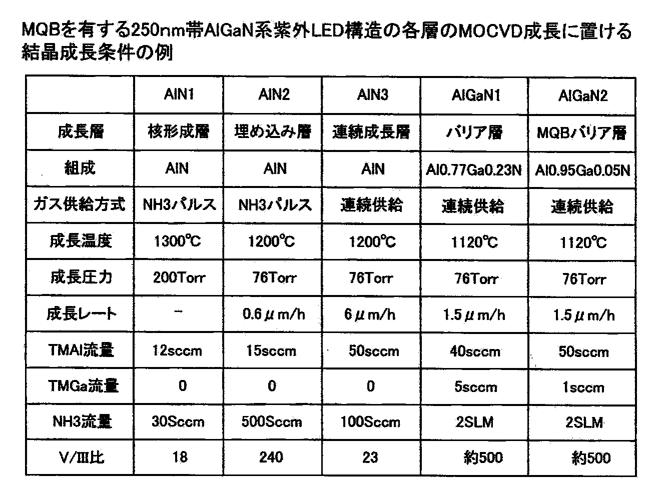
表1に用いたMOCVDの成長条件の例を、「アンモニアパルス供給多段成長法」形成AlNバッファの核形成層(3a)(アンモニアパルス成長:成長条件AlN1)、パルス成長埋め込み層(3b)(アンモニアパルス成長:成長条件AlN2)、連続成長AlN(3c)(成長条件AlN3)について、また250nm帯AlGaN量子井戸LEDの、バリア層(成長条件AlGaN1)、MQBバリア層(成長条件AlGaN2)について示す。
次に、紫外(深紫外)発光素子の特性について説明する。


波長249nmでは、EQEの最大値が1.50%、最高出力が8.7mWとなっている。また、波長250nmでは、EQEの最大値が1.15%、最高出力が15.0mWとなっている。波長262nmでは、EQEの最大値が1.54%、最高出力が10.4mWとなっており、このような高い値が得られている。
上記の表1に用いたMOCVDの成長条件の例を、「アンモニアパルス供給多段成長法」形成AlNバッファの核形成層(3a)(アンモニアパルス成長:成長条件AlN1)、パルス成長埋め込み層(3b)(アンモニアパルス成長:成長条件AlN2)、連続成長AlN(3c)(成長条件AlN3)について、また250nm帯AlGaN量子井戸LEDの、バリア層(成長条件AlGaN1)、MQBバリア層(成長条件AlGaN2)について示す。AlNバッファーを成長する条件としては、AlN結晶のクオリティを高めるため、一般的にGaNあるいはAlGaNで用いている成長温度(1000−1120℃)より高い温度(1200−1300℃)を用いており、また、V/III比(V族元素の供給量とIII族元素の供給量のモル比)も、一般的にGaNあるいはAlGaNで用いられる値(2000以上)に比べ低い値を用いている。また、MQBのバリア層の成長条件としては、一般的なAlGaNの成長条件を用いており、減圧横型MOCVD装置により、成長温度を1120℃、成長圧力を76Torr(133.32Pa=1Torr)とし、供給量を、TMGが1sccm、TMAが50sccm(1sccm=1.667x10−5 l/s)、NH3が2000sccmなどを用いて成長を行っている。
尚、用いたMOCVD装置の詳細に関しては、例えば発明者らの特許文献である、特開2004−228489号の図2、図7から9及びその記載を参照することにより実施可能であるため、ここでは説明を省略する。
図3は、多重量子障壁について一般的な単一電子ブロック層と比べた利点を模式的に示した図面である。図は250nm帯AlGaN量子井戸LEDのAl組成のプロファイルを示したものであるが、同時に、無極性結晶の場合のLED動作時のバンドプロファイルと傾向はほぼ一致すると考えられる。したがってMQBの効果を一般的に説明する上で有用な図である。C面上に成長した極性の強い結晶におけるバンドプロファイルは、後述図9のようにバンドの傾きを考慮する必要があり、やや理解が複雑である。図3(b)に示すようにAl0.95Ga0.05N:Mg(25nm)の電子に対するシングルバリアの場合は、その高さ以下のエネルギーを有する電子をほぼ完全に反射することが出来るが、バリア以上の高さの電子についてはほとんど反射することができない。したがって電子バリア高さは、伝導帯のバンド不連続値でリミットされてしまう。図3(a)に示すように、Al0.95Ga0.05N(4nm)/Al0.77Ga0.23N(2nm)を5層ずつ形成したMQBでは、量子力学的な電子の反射効果により、バリア高さ以上の高いエネルギーを有する電子も反射することができる。
従って、シングルバリア(SQB)の場合には、電子ブロック高さはSQBを構成する材料によってその限界が決定されるのに対し、MQBでは材料リミットに加え、量子力学的な多層反射効果でバリア高さをさらに増加させることが可能である。後述のように、実効的なバリア高さは、各層のバリア高さと厚みとを最適化することにより、最大で3.5倍程度に向上させることが可能である。
これまでの発明者らの研究で、電子ブロック層に最もバリア高さの高いAlNあるいはAl組成95%のAlGaNを用いた場合でも、AlGaN紫外LEDの電子注入効率は10−30%(240−280nm帯LEDに対して)と低く、紫外LED高効率化の大きな妨げとなっていた。また、この低い電子注入効率は、p型AlGaNの低いホール濃度に起因するものであるため、解決できないものとされてきた。本発明提案の設計指針により形成されたMQBを利用すれば、上記問題は根本的に解決されると考えられ、MQB効果は、AlGaN系高効率紫外LEDを実現する上できわめて重要である。
また、p側層への電子リークは、注入電流密度の増加に伴って起こる、発光層領域におけるキャリア密度の増大によって、拍車をかけて増加する。紫外LDの注入電流密度は紫外LEDの場合の10−100倍程度になるため、電子注入効率はさらに低くなり、電流密度が発振閾値に達しないうちに過熱により破壊すると考えられる。また発振したとしても、高出力を得るのが不可能である。MQBは上述のように、高い電子ブロック高さを実現することが特徴であるため、キャリア密度の増大による高いエネルギーの電子を反射することに大きな効果を発揮し、紫外LDの発振と高効率化に大きく寄与できると考えられる。また、高注入電流時に高い電子注入効率が得られることから、紫外LEDにおいてドゥループの少ない動作が可能であり、高出力時にも効率が減少しない安定した紫外LEDを提供できる。
また、近年商品化が進んでいる白色ランプ用の青色LEDでは、低電流動作時には非常に高い外部量子効率(EQE)が得られるもの、高出力動作時のEQEが低下するドゥループが大きな問題となっている。ドゥループの発生に関しては、紫外LEDの場合と同様、高電流注入時の電子のリークによる電子注入効率の低下がひとつの要因であると考えられる。ドゥループを改善するためには十分に電子バリア高さの高い電子ブロック層を導入することが重要である。したがって、高いAl組成(20−50%)のAlGaN電子ブロック層を挿入することが解決策として考えられる。しかし、低抵抗のp型層伝導と歪のマネージメントを考えると、そのような高いAl組成のAlGaN電子ブロック層を青色LEDに用いた場合、かえってデバイス効率を低下させ望ましくない。一方、MQBを用いれば、10%以下の低いAl組成のバリア層を用いてもその数倍の実効的電子ブロック高さを実現することができ、低Al組成で最大限の効果を引く出すことが出来る。したがって、低抵抗のp型層伝導と各層の低歪を実現しながらドゥループを改善することができる。このようにMQBの利用により、高電流注入時の効率を改善し、青色LEDの安定した高出力動作が可能になり、重要性が高い。MQBの効果は、同様に、近紫外、緑色発光素子においても大変有用であると考えられ、波長220−550nmの広い波長範囲の窒化物発光素子の高効率化において大変重要性が高い。
図4は、多重量子障壁を用いたAlGaN量子井戸紫外LED(波長250−262nm)の室温動作発光特性を示す図である。図4に示すように、250nmと262nmにおいて、いずれも、きれいなシングルピークが現れており、不純物などに起因するその他の発光は1/100程度に小さいことがわかる。このように、本実施の形態による深紫外発光素子では、発光素子としてすぐれた特性が得られることがわかる。
図5は、多重量子障壁を用いた電子ブロック層によるAlGaN量子井戸紫外LEDの効率向上を波長250nmにおいて示した例である。比較として、単一電子ブロック層(EBL)を用いたものの特性を示す。縦軸は、図5(a)が紫外光出力、図5(b)がEQE(外部量子効率)である。このように、この図では、250nmAlGaN型LEDで、約4倍の外部量子効率の向上を実現することができる。
図6は、多重量子障壁を用いた262nmAlGaN紫外LEDの動作特性を示す図である。図6に示すように、EQEとして1.54%、出力電力として10.4mWの良好な特性を得ることができた。
表2は現段階で得られている250−260nm付近波長AlGaN量子井戸紫外LEDのEQEと出力についてまとめたものである。AlGaN各層のAl組成も同時に示した。
波長249nmでは、EQEの最大値が1.5%、最高出力が8.7mWが得られている。また、波長262nmでは、EQEの最大値が1.54%、最高出力が10.4mWが得られている。また、250nmで15.0mW連続出力が得られている。これらの値は、すべて現時点でのトップデータである。
殺菌用途として紫外LEDを使った場合、連続10mW出力は、20cmはなれた距離から照射した場合、約1分でバクテリアを99%以上殺菌できる強度である。したがって、家庭用などの殺菌用途として用いる場合の実用化へのひとつの出力の目あすとなる出力である。MQBを用いたAlGaN系紫外LEDでは上記のようにそれを大きく上回り、実用レベル出力を達成している。
図7は、多重量子障壁(MQB)電子ブロック層を用いたことによる、外部量子効果向上の効果(波長依存性)を示す図である。単一障壁による電子ブロック層を用いた場合に比べて、多重量子障壁による電子ブロック層を用いると、大きな外部量子効率が得られることがわかる。室温においても大きな値が得られる。ここでは、250nmから260nm帯において顕著な効果が得られている。MQBを用いたAlGaN量子井戸LEDのEQEの最高値(249nmにおいて1.5%)は、従来のSQBを用いた0.4%に対し約4倍の改善が見られた。また最高出力(250nmで15.0mW)は、250nmでは従来のSQBを用いた場合の2.2mWに対し、約7倍の出力が得られた。MQB構造の最適化により、一層の効率・出力向上が可能である。また、220nmから390nmの広い紫外領域で同様の効果が得られる。
得られた紫外AlGaN量子井戸LEDの外部量子効率に関してその内訳を議論する。

MQBを有する250nm帯のAlGaN量子井戸LED(最高EQE:1.5%)についてその内訳を推測する。IQEは同構造のサンプルのフォトルミネッセンス(PL)発光の温度依存性から、30%程度と見積もられる。また、LEEは素子の構造から計算し6%程度と見積もられる。外部量子効率をIQE、LEEで割ることにより、電子注入効率(EIE)は83%と推測される。一方、シングル電子ブロック層を有する同LEDではEQEが0.4%であり、IQE,LEEはほぼ同レベルであるため、EIEは22%と推測される。したがって、MQB導入により電子注入効率は22%から83%程度に増加しており、その効果は絶大である。本結果から、p型AlGaNの低ホール濃度に起因する電子注入効率低下の問題は、MQB導入によりほぼ解決されることが分かる。
図8は、本発明の実施例によるMQBを利用したMQW型LEDの一構成例を示すエネルギーバンド構造であり、A面上に成長した極性のないLEDの伝導帯の端を示す図である。図8(a)に示す構造では、Al組成が、井戸/障壁/MQBでそれぞれ、50%/70%/95%の場合であり(バリア高さが高い場合)、図8(b)に示す構造では、Al組成が、井戸/障壁/MQBでそれぞれ、75%/85%/95%の(バリア高さが低い場合)場合の例である。図8、図9とも、電極間に電圧を印加した動作状態でのエネルギーバンド図を示すものである。MQBで反射された電子は、MQW中に落ちて発光効率を向上させる。
極性の無い場合のLEDの動作時のバンドプロファイルは、電子・ホールを輸送するため若干傾きはあるものの、図8(a)などに示すようにほぼ平らなバンド構造と置き換えて考えても、MQBの効果を一般的に説明する上で差し支えない。図8(a)は270nm帯AlGaN量子井戸LEDを想定したもので、MQBのバリア高さが0.6eV程度と大きい場合を仮定している。一方、図8(b)は230nm帯AlGaN量子井戸LEDを想定しており、MQBのバリア高さが0.3eV程度と比較的小さい場合を仮定している。
図9(c)及び(d)は、図8(a)及び(b)と同様のLED層構造であるが、C面上に結晶成長した強い極性のある場合の例である。窒化物半導体では、ウルツ鉱構造(六方晶)の結晶構造が一般的に用いられ、結晶成長において高品質結晶が得られやすいC面上への成長がよく用いられる。特にAlGaNの結晶成長において、非極性面(A面、あるいはM面)の成長は、平坦性を得るのが大変難しいため、非極性面では良質なAlGaN量子井戸はまだ実現されておらず、高効率紫外発光は得られていない。したがって、C面上に成長した場合の検討が重要である。尚、窒化物半導体では、A面、M面はよく知られた極性面である。
図9(c)、(d)に示すように、AlGaN系ヘテロ構造では非常に大きな自然分極、ピエゾ電極が自動的に印加され、バンド構造の解析は大変複雑である。図9(c)及び(d)の各層の傾きは、各層の結晶がn型AlGaNバッファ層に格子マッチングしていると仮定し、各層のAl組成における自然分極とピエゾ分極の大きさを、報告されている値から求め、さらに、LED動作時の電子、ホールのギフェルミ準位の傾きを考慮に入れて描いたものである。
図に示されるように、AlGaNバリアと井戸のAl組成の差が大きいほど、ピエゾ分極が大きく各層のバンド傾きが大きくなることが分かる。270nmAlGaN量子井戸LEDを想定した場合では、MQB電子ブロック層のバリア及びバレイ領域で大きなピエゾ分極が発生し、またそれにより各バリア層のエネルギー位置がずれて配置されるため、MQBの電子反射効果が予測しにくい。また、量子井戸のバンド傾きが特に大きく、電子閉じ込めが弱くなることによる電子のリーク、発光準位の電子・ホール波動関数の重なり積分値の低下による発光効率の低減なども予測される。このように、極性の影響がバンド構造に与える影響は大きいことがわかる。図9(d)は、230nm帯LEDを同定し、MQBを構成するAlGaNのバリア組成とバレイ組成差が10%と小さい場合のバンドプロファイルである。図9(c)に比べ分極によるバンド傾きが半分程度に小さいが、まだMQB効果や量子井戸閉じ込めに対する影響は大きい。
図10A(a)から(d)、図10B(e)から(h)までは、図8(a)に対応する高めのバリアのA面上に成長した極性のないLEDにおいて、2ML(モノレーヤー)から15MLまでの井戸厚/バリア厚の場合と、20nmのシングルバリアの場合の電子の透過率のエネルギー依存性を示す図である。
シングルバリアを示す図10B(h)をみると分かるように、シングルバリアの場合にはバンドエッジより高い領域にはほとんど反射エネルギー帯が形成されていない。シングルバリアの厚さをもっと厚くした場合(たとえば50nm)でも、その特定は変わらず、量子力学的な反射率は、バンドエッジ以上のエネルギーにおいて改善されない。現在用いられているシングル電子ブロック層の導入において、その厚さを増やすと電子ブロック効果が大きくなる現象は、電子の拡散とドリフトが厚い電子ブロック層で減少し、それによってp側層へのリークを抑える効果であり、量子力学的な効果ではない。MQBでは量子力学的な電子の多重反射効果を用いることを特徴としている。
図10に示されるように、障壁と井戸との周期が短くなればなるほど、量子力学的な効果により、高いエネルギー帯に電子の反射領域が形成されていることがわかる。また、厚めのバリア(たとえば7ML以上の場合)を用いた場合は、複数の反射バンド帯が発生する。その結果反射エネルギー帯は、たとえば、2ML,3ML,4ML,5ML,7ML,10ML,15MLのバリア/バレイMQBにおいて、1.7−2.2eV,0.8−1.2eV,0.55−0.9eV,0.35−0.75eV,0.65eV以下と0.8−1.0eV,0.75eV以下、0.7eV以下となる。障壁層と井戸の周期が短い場合は、反射バンドよりも低いエネルギー帯に透過率の高い透過バンド帯が形成される。透過バンド帯は、例えば、3ML、4ML、5ML、7MLのバリア/バレイMQBでは、0.3−1.7eV,0.3−0.85eV,0.25−0.55eV,0.25−0.35eV,0.65−0.8eVに形成される。したがってこのままの構造では使いにくいことがわかる。実際に用いる構造では、電子の透過帯を発生させないようにすることが重要であり、複数の周期の障壁/井戸を組み合わせて構成する必要がある。
窒化物半導体のMQBの大きな特徴は、効果が期待されるバリアの厚さが2ML~10MLなどと大変薄いことである。これはInP系やGaAs系など従来の半導体との大きな違いであり、その膜厚は5倍程度薄い。これは電子の有効質量がInP系半導体などに比べ1/5程度に小さいことに起因している(電子の有効質量:0.04(InP)、0.2(GaN))。
薄いバリア周期で高い反射効果が得られるため、媒質における電子のコヒーレンス長以内の領域でMQB効果を充分得ることが可能である。このことはAlN−GaN系材料を用いる一つの大きなメリットである。これは、コヒーレンスが得られない領域では量子力学的な電子の反射効果が半減してしまうため重要な事項である。
一方、窒化物半導体MQBでは数モノレーヤー周期の構造を作る必要があり、原子層1層の制度で行われる非常に緻密な結晶成長法が必要である。MOCVDを用いたAlGaN成長において、発明者らはすでに5ML(1.3nm膜厚)の多重量子井戸を用いており、TEM(透過電子顕微鏡)を用いた評価により、原子1層の精度でヘテロ界面の組成の切り替えができていることを確認している。また、3ML厚量子井戸での発光も観測している。したがって、2ML~10MLのMQBバリア層の膜厚の制御は、現状技術を用いて可能であると考えられる。
[実施例1]
図11(a)、(b)は、図10の結果に基づいて、単一バリアとMQBとを用いた場合の、電子の透過率のエネルギー依存性を示す図である。バリアのバンド端のエネルギーよりもできるだけ高いエネルギーにわたって高い電子反射が得られるように、いくつかのバリア周期を組み合わせて用いている。図11(a)は、MQW側から順番に、バリアの周期が順番に大きくなっていく構造例を示すMQBを示す図であり、図11(b)は周期の順番がその逆である例を示す図である。いずれの場合においても、図10に示す例に比べて電子の透過率のエネルギー依存は広い範囲にわたって低くなっており、電子ブロック層としての有用性が高いことがわかる。実効的なバリア高さは、シングルバリアのときに比べ約3.5倍高くなっている。
尚、図11(a)、(b)を比較すると、量子力学的解析において、周期の順番に関する依存性は無いことが分かる。しかし実際の動作においては、電子のコヒーレンス長以上の距離の構造では電子反射効果が減少し、効果に差が出てくる可能性がある。半導体中のコヒーレンス長を考えれると、MQB領域のトータル膜厚(総厚)が~40nm以下であることが望ましい。また、より低いエネルギー領域で電子濃度が高いため、低いエネルギーの電子をまずブロックし、その後高いエネルギーの電子をブロックする方式が理にかなっている。したがって、図(b)に示すように、量子井戸に隣接して周期の大きなものから小さなものへ変化させたMQBのほうが一般的には効果が得られやすいと考えられる。
図12は、A面上に成長した極性のないMQBの場合における、電子の透過率のエネルギー依存に関する、周期を異ならせたMQB層の総厚依存性を示す図である。総厚が大きいほど、電子は高いエネルギー値まで反射されることがわかる。これは、多くの種類のMQBを有するほど、電子の反射が多くのエネルギー範囲で生じることから、電子の反射の効果が高まることがわかる。図から、MQBの総厚を20nmと小さくした場合でも、MQBによる実効的バリア高さは、シングルバリアの2倍程度得られており、薄い総厚のMQBでも大きな反射効果が得られることが分かる。
図13A(a)から図13B(h)までは、図8(a)に対応する低めのバリアのA面上に成長した極性のないMQBの場合における、電子の透過率のエネルギー依存性を示す図である。この場合には、高めのバリア(図11)を用いた時、周期と反射エネルギー帯の関係はほぼ同様であるが、反射エネルギー帯が狭くなる。また、電子の反射率は低くなる。したがって、低いバリアのMQBを用いた場合、バリアの周期数を増やすなどの設計が必要となる。
図14は、A面上に成長した極性のないMQB(低いバリア;図13)の場合における、電子の透過率のエネルギー依存に関する、周期を異ならせたMQB層の総厚依存性を示す図である。総厚が大きいほど、電子は高いエネルギー値まで反射されることがわかる。但し、図12の場合に比べると、低いエネルギーまでしか電子を反射させることができない。図14(b)、図14(c)に示すように、層の総厚が大きいほど、高いエネルギーまで電子を反射させることができ、たとえば、総厚60nm程度の場合は実効的バリア高さは3倍、総厚25nm程度の場合は約2倍が得られている。25nmの総厚でも充分な実効的高さが得られることから、Al組成差で10%程度の低いバリア高さを用いた場合でも大きなMQB効果が得られることが分かった。
実際のMQB設計において、広いエネルギー帯で透過帯を形成せず、高い反射率を実現する設計はやや複雑である。したがって、どの周期のバリアを何層ずつ組み合わせればよいのか、その指針を示す必要がある。
図15(a)、(b)は、バリアが高い時とバリアが低い時における、A面上に成長(極性なし)した場合における、周期別のエネルギーの電子透過率依存性を示す図である。これらの図に示されるように、バリアが高いほど、広いエネルギー範囲で電子を反射することができることがわかる。さらに、周期が短いほど電子の透過率が高くなり、すなわち、周期が長いほど電子をブロックできることがわかる。カラー図面を参照すると、より良く特性が理解できる。
図16は、本実施例によるバリア高さをパラメータとしたMQBの周期と電子の透過率との関係を示す図である。図16に示すように、高いバリアと低いバリアとで、3ML/3MLの周期でMQBを作成した場合における、透過率のMQBの周期の依存性を示す図である。図に示すように、MQBの周期数が多いほど、電子の透過率が低くなる。また、バリア高さが高いほど、同じ周期数でも電子の透過率が低くなることがわかる。
以上のように、バリア高さが高いほど、MQBの周期が長いほど、電子のブロック効果が向上することがわかる。
実際のMQBでは周期の異なるバリア層を複数組み合わせて構成する。MQB全体の反射率は、各部分のバリアの反射率の足し合わせでほぼ決まることが解析から明らかである。したがって、各周期のバリアにおいて、高反射が得られる反射エネルギー帯と目安となる周期数が分かっていれば設計が簡略に行える。表3に高反射が得られる反射エネルギー帯と目安となるバリア周期数の数値をまとめる。
[実施例2]
以下においては、C面上に成長した極性のある結晶の場合の特性について説明する。図17Aから図20までは、上記第1の実施の形態とほぼ同じであるが、A面ではなくC面に成長したMQBの場合の特性を示す図である。極性がある場合のMQB効果の傾向は、極性が無い場合の効果と基本的に同様であるが、バンドの傾きの影響で反射率にボケが生じるなどやや複雑である。極性のある場合の特徴について以下記述する。
極性がある場合は、シングルバリアの場合でもバリアのエネルギーが鋸刃状になるため、極性の無い時に比べもともと高い電子バリアを形成している。したがって、MQBによる実効的バリア高さの増加分は、極性が無い時に比べれば小さくなる。
MQBバリアの形状を鋸刃状に盛り上げ、できるだけ高さのあるバリアとするために、バリア/バレイの膜厚の比を大きくとることが望ましい。すなわちバリア/バレイ厚さを同じにするのではなく、3/2ML,5/2ML,10/2ML、15/2MLなどとすることによって、バリアの頂点部を高く形成することができる。同様に、MQBバリアの形状を鋸刃状に盛り上げるためには、厚いバリアから順番に配列することが重要である。
図17に示すように、単一バリアの場合と比較して、MQBを用いた場合には、同じような高さ・厚さであっても、電子をブロックする効果が高いことがわかる。極性により各バリア層のエネルギー高さが異なるため、無極性の時に比べると、反射帯の得ネルビー分布がブロードで反射率もやや低い。
図18ではバリアが高い時に関してMQB効果のMQB総厚依存性を示した。MQB総厚45nmで実効的バリア高さは単一バリア比べて約2倍、MQB総厚30nmの時には約1.5倍が得られ、通常のC面上で極性ありの場合でも大きな実効的バリア高さが確保できることが分かる。
図19は同様にバリアが低い時の反射率の解析例である。分極の影響は、Al組成比が大きい場合に比べ減少しているが、分極による反射率のブロードニング効果は依然無視できない。図20ではバリアが低い時に関してMQB効果のMQB総厚依存性を示した。MQB総厚40nmのとき実効的バリア高さは単一バリア比べて約1.3倍、MQB総厚55nmの時には約1.5倍が得られ、MQBの全体の厚さが小さい時であっても、大きい時であっても、電子のブロック効果は単一バリアの場合に比べて良好であることがわかる。
これらの結果から、C面上に成長した極性のある結晶の場合でも、極性がない場合と同様の実効的バリア高さの大きな増加が得られることがわかる。
なお、上記では、紫外発光素子を例にして説明したが、本発明による多重量子障壁構造は、その他の発光波長を有する窒化物半導体発光素子にも利用可能である。
(近紫外、紫、青、緑のドゥループ改善、LD効率改善)
すなわち、近年商品化が進んでいる白色ランプ用の青色LEDでは、低電流動作時には非常に高い外部量子効率(EQE)が得られるもの、高出力動作時のEQEが低下するドゥループが大きな問題となっている。ドゥループの発生に関しては、紫外LEDの場合と同様、高電流注入時の電子のリークによる電子注入効率の低下がひとつの要因であると考えられる。ドゥループを改善するためには十分に電子バリア高さの高い電子ブロック層を導入することが重要である。したがって、高いAl組成(20−50%)のAlGaN電子ブロック層を挿入することが解決策として考えられる。しかし、低抵抗のp型層伝導と歪のマネージメントを考えると、そのような高いAl組成のAlGaN電子ブロック層を青色LEDに用いた場合、かえってデバイス効率を低下させ望ましくない。一方、MQBを用いれば、10%以下の低いAl組成のバリア層を用いてもその数倍の実効的電子ブロック高さを実現することができ、低Al組成で最大限の効果を引く出すことが出来る。したがって、低抵抗のp型層伝導と各層の低歪を実現しながらドゥループを改善することができる。このようにMQBの利用により、高電流注入時の効率を改善し、青色LEDの安定した高出力動作が可能になり、重要性が高い。MQBの効果は、同様に、近紫外、緑色発光素子においても大変有用であると考えられ、波長220−550nmの広い波長範囲の窒化物発光素子の高効率化において大変重要である。
(まとめ)
MQBを用いると、単一バリアの場合と比べて、電子のブロック効果が高まることがわかる。
また、A面に成長した場合においても、C面上に成長した極性のある結晶の場合においても、バリア高さが高いほど、MQBの周期が長いほど、電子のブロック効果が良くなることがわかる。
さらに、MQBを用い、その周期を順番に変化させることにより、広いエネルギー範囲にわたって、電子をブロックすることができ、同じ周期のMQBに比べてより電子ブロック効果が顕著であることがわかる。
(発明の効果)
本実施の形態においては、以下の効果が得られる。
1)紫外LEDの電子注入効率向上
2)紫外LEDのドゥループ改善
3)紫外LD発振
4)近紫外、紫、青、緑のドゥループ改善、LD効率改善
より詳細には、以下の通りである。
(紫外LEDの電子注入効率向上)
これまでの発明者らの研究で、電子ブロック層に最もバリア高さの高いAlNあるいはAl組成95%のAlGaNを用いた場合でも、AlGaN紫外LEDの電子注入効率は10−30%(240−280nm帯LEDに対して)と低く、紫外LED高効率化の大きな妨げとなっていた。また、この低い電子注入効率は、p型AlGaNの低いホール濃度に起因するものであるため、解決できないものとされてきた。本特許提案の設計指針により形成されたMQBを利用すれば、上記問題は根本的に解決されると考えられ、MQB効果は、AlGaN系高効率紫外LEDを実現する上できわめて重要である。
(紫外LD実現)
また、p側層への電子リークは、注入電流密度の増加に伴って起こる、発光層領域におけるキャリア密度の増大によって、拍車をかけて増加する。紫外LDの注入電流密度は紫外LEDの場合の10−100倍程度になるため、電子注入効率はさらに低くなり、電流密度が発振閾値に達しないうちに過熱により破壊すると考えられる。また発振したとしても、高出力を得るのが不可能である。MQBは上述のように、高い電子ブロック高さを実現することが特徴であるため、キャリア密度の増大による高いエネルギーの電子を反射することに大きな効果を発揮し、紫外LDの発振と高効率化に大きく寄与できると考えられる。
(紫外LEDのドゥループ改善)
また、高注入電流時に高い電子注入効率が得られることから、紫外LEDにおいてドゥループの少ない動作が可能であり、高出力時にも効率が減少しない安定した紫外LEDを提供できる。
(近紫外、紫、青、緑のドゥループ改善、LD効率改善)
また、近年商品化が進んでいる白色ランプ用の青色LEDでは、低電流動作時には非常に高い外部量子効率(EQE)が得られるもの、高出力動作時のEQEが低下するドゥループが大きな問題となっている。ドゥループの発生に関しては、紫外LEDの場合と同様、高電流注入時の電子のリークによる電子注入効率の低下がひとつの要因であると考えられる。ドゥループを改善するためには十分に電子バリア高さの高い電子ブロック層を導入することが重要である。したがって、高いAl組成(20−50%)のAlGaN電子ブロック層を挿入することが解決策として考えられる。しかし、低抵抗のp型層伝導と歪のマネージメントを考えると、そのような高いAl組成のAlGaN電子ブロック層を青色LEDに用いた場合、かえってデバイス効率を低下させ望ましくない。一方、MQBを用いれば、10%以下の低いAl組成のバリア層を用いてもその数倍の実効的電子ブロック高さを実現することができ、低Al組成で最大限の効果を引く出すことが出来る。したがって、低抵抗のp型層伝導と各層の低歪を実現しながらドゥループを改善することができる。このようにMQBの利用により、高電流注入時の効率を改善し、青色LEDの安定した高出力動作が可能になり、重要性が高い。MQBの効果は、同様に、近紫外、緑色発光素子においても大変有用であると考えられ、波長220−550nmの広い波長範囲の窒化物発光素子の高効率化において大変重要性が高い。
本明細書で引用した全ての刊行物、特許および特許出願をそのまま参考として本明細書にとり入れるものとする。
Claims (10)
- 基板に形成されたAlxGa1−xN(0<x<1)バッファ層と、
前記AlxGa1−xNバッファ層上に形成されたn型InxAlyGa1−x−yN(0<x<0.1,0<y<1)層と、
前記n型InAlGaN層上に形成されたInx1Aly1Ga1−x1−y1N(0<x1<0.5,0<y1<1)量子井戸層とInx2Aly2Ga1−x2−y2N(0<x2<0.3,0<y2<1,x1>x2,y1<y2)バリア層からなる量子井戸発光層と、
前記InAlGaN量子井戸発光層上に形成されたp型InxAlyGa1−x−yN(0<x<0.1,0<y<1)層と、
前記p型InAlGaN層上に形成された多重量子障壁電子ブロック層と、
を備えた波長220~390nmで発光する窒化物半導体発光素子。 - 前記多重量子障壁電子ブロック層として、
Inx1Aly1Ga1−x1−y1N(0<x1<0.1,0<y1<1)バリア層とInx2Aly2Ga1−x2−y2N(0<x2<0.3,0<y2<1,x1<x2,y1>y2)バレイ層を、同一周期、または、第1の周期及び前記第1の周期とは異なる第2の周期の層で多層積層した多重量子障壁電子ブロック層を有することを特徴とする、請求項1に記載の発光素子。 - 基板に形成されたAlxGa1−xN(0<x<1)バッファ層と、
前記AlxGa1−xNバッファ層上に形成されたn型InxAlyGa1−x−yN(0<x<0.1,0<y<1)層と、
前記n型InAlGaN層上に形成されたInx1Aly1Ga1−x1−y1N(0<x1<0.5,0<y1<1)量子井戸層とInx2Aly2Ga1−x2−y2N(0<x2<0.3,0<y2<1,x1>x2,y1<y2)バリア層からなる量子井戸発光層と、
前記InAlGaN量子井戸発光層上に形成されたp型InxAlyGa1−x−yN(0<x<0.1,0<y<1)層と、
前記p型InAlGaN層上に形成された多重量子障壁電子ブロック層と、
を備え、
前記多重量子障壁電子ブロック層として、
Inx1Aly1Ga1−x1−y1N(0<x1<0.1,0<y1<1)バリア層とInx2Aly2Ga1−x2−y2N(0<x2<0.3,0<y2<1,x1<x2,y1>y2)バレイ層を、同一周期、または、第1の周期及び前記第1の周期とは異なる第2の周期の層で多層積層した多重量子障壁電子ブロック層を有することを特徴とする、波長390~550nmで発光する、近紫外、紫、青、又は、緑色窒化物半導体発光素子。 - 前記活性層側から前記多重量子障壁電子ブロック層側に向けて、前記周期が、順次大きくなるか或いは順次小さくなることを特徴とする請求項1または3に記載の窒化物半導体発光素子。
- 前記多重量子障壁電子ブロック層は、A面,M面上に形成された極性の無い層、あるいは半極性面に形成された層であることを特徴とする請求項1から4までのいずれか1項に記載の窒化物発光素子。
- III族窒化物単結晶上に形成する発光素子構造の成長方法において、
基板上にAlxGa1−xN(0<x<1)バッファ層を成長するステップと、
前記AlxGa1−xNバッファ層上にn型InxAlyGa1−x−yN(0<x<0.1,0<y<1)層を成長するステップと、
前記n型InAlGaN層上にInx1Aly1Ga1−x1−y1N(0<x1<0.5,0<y1<1)量子井戸層とInx2Aly2Ga1−x2−y2N(0<x2<0.3,0<y2<1,x1>x2,y1<y2)バリア層からなる量子井戸発光層を成長するステップと、
前記InAlGaN発光層上にp型InxAlyGa1−x−yN(0<x<0.1,0<y<1)層を成長するステップと、
前記p型InAlGaN層上にInx1Aly1Ga1−x1−y1N(0<x1<0.1,0<y1<1)バリア層とInx2Aly2Ga1−x2−y2N(0<x2<0.1,0<y2<1,x1<x2,y1>y2)バレイ層を多層積層した多重量子障壁電子ブロック層を成長するステップと、を有することを特徴とする発光素子構造の成長方法。 - 前記p型InAlGaN層上に形成された多重量子障壁電子ブロック層は、Inx1Aly1Ga1−x1−y1N(0<x1<0.1,0<y1<1)バリア層とInx2Aly2Ga1−x2−y2N(0<x2<0.3,0<y2<1,x1<x2,y1>y2)バレイ層との対が複数形成され、
第1の対の層と第2の対の層はそれぞれ離れており、前記第1の対の層の層厚の方が前記第2の対の層の層厚より厚いか、或いは、前記第1の対の層の層厚の方が前記第2の対の層の層厚より薄く、かつ、
前記量子井戸発光層側の側から前記基板と反対側の方に向かって、前記第1の対の層と前記第2の対の層がその順番で設けられていることを特徴とする請求項1に記載の窒化物半導体紫外発光素子。 - 前記p型InAlGaN層上に形成された多重量子障壁電子ブロック層は、Inx1Aly1Ga1−x1−y1N(0<x1<0.1,0<y1<1)バリア層とInx2Aly2Ga1−x2−y2N(0<x2<0.3,0<y2<1,x1<x2,y1>y2)バレイ層との対が複数形成され、
第1の対の層、第2の対の層および第3の対の層はそれぞれ離れており、前記第1の対の層の層厚の方が前記第2の対の層の層厚より厚く、前記第2の層の対の層厚が前記第3の対の層より厚いか、或いは、前記第1の対の層の層厚の方が前記第2の対の層の層厚より薄く、前記第2の層の対の層厚が前記第3の対の層より薄く、かつ、
前記量子井戸発光層側の側から前記基板と反対側の方に向かって、前記第1、第2および第3の層の対がその順番で設けられていることを特徴とする請求項1に記載の窒化物半導体紫外発光素子。 - 前記対の層における前記バリア層と前記バレイ層とが同じ分子層数であることを特徴とする請求項7又は8に記載の窒化物半導体紫外発光素子。
- 発光ダイオードであることを特徴とする請求項7から9までのいずれか1項に記載の窒化物半導体紫外発光素子。
Priority Applications (5)
| Application Number | Priority Date | Filing Date | Title |
|---|---|---|---|
| KR1020127024827A KR101422979B1 (ko) | 2010-02-24 | 2010-11-25 | 질화물 반도체 다중 양자 장벽을 갖는 발광 소자 및 그 제조 방법 |
| JP2012501649A JP5843238B2 (ja) | 2010-02-24 | 2010-11-25 | 窒化物半導体多重量子障壁を有する発光素子及びその製造方法 |
| KR1020147010749A KR101636182B1 (ko) | 2010-02-24 | 2010-11-25 | 질화물 반도체 다중 양자 장벽을 갖는 발광 소자 및 그 제조 방법 |
| US13/580,868 US8759813B2 (en) | 2010-02-24 | 2010-11-25 | Light-emitting element having nitride semiconductor multiquantum barrier, and process for production thereof |
| US14/268,267 US9059354B2 (en) | 2010-02-24 | 2014-05-02 | Light-emitting element having nitride semiconductor multiquantum barrier, and process for production thereof |
Applications Claiming Priority (2)
| Application Number | Priority Date | Filing Date | Title |
|---|---|---|---|
| JP2010038912 | 2010-02-24 | ||
| JP2010-038912 | 2010-02-24 |
Related Child Applications (2)
| Application Number | Title | Priority Date | Filing Date |
|---|---|---|---|
| US13/580,868 A-371-Of-International US8759813B2 (en) | 2010-02-24 | 2010-11-25 | Light-emitting element having nitride semiconductor multiquantum barrier, and process for production thereof |
| US14/268,267 Continuation US9059354B2 (en) | 2010-02-24 | 2014-05-02 | Light-emitting element having nitride semiconductor multiquantum barrier, and process for production thereof |
Publications (1)
| Publication Number | Publication Date |
|---|---|
| WO2011104969A1 true WO2011104969A1 (ja) | 2011-09-01 |
Family
ID=44506405
Family Applications (1)
| Application Number | Title | Priority Date | Filing Date |
|---|---|---|---|
| PCT/JP2010/071524 Ceased WO2011104969A1 (ja) | 2010-02-24 | 2010-11-25 | 窒化物半導体多重量子障壁を有する発光素子及びその製造方法 |
Country Status (4)
| Country | Link |
|---|---|
| US (2) | US8759813B2 (ja) |
| JP (1) | JP5843238B2 (ja) |
| KR (2) | KR101636182B1 (ja) |
| WO (1) | WO2011104969A1 (ja) |
Cited By (23)
| Publication number | Priority date | Publication date | Assignee | Title |
|---|---|---|---|---|
| US20120187365A1 (en) * | 2011-01-26 | 2012-07-26 | Lg Innotek Co., Ltd. | Light emitting device |
| US20130082237A1 (en) * | 2011-10-04 | 2013-04-04 | Palo Alto Research Center Incorporated | Ultraviolet light emitting devices having enhanced light extraction |
| CN103296170A (zh) * | 2012-11-19 | 2013-09-11 | 浙江优纬光电科技有限公司 | 一种AlGaN基深紫外LED器件及其制造方法 |
| WO2014069235A1 (ja) * | 2012-11-02 | 2014-05-08 | 独立行政法人理化学研究所 | 紫外発光ダイオードおよびその製造方法 |
| JP2014096539A (ja) * | 2012-11-12 | 2014-05-22 | Tokuyama Corp | 紫外発光素子、および発光構造体 |
| JP2015119108A (ja) * | 2013-12-19 | 2015-06-25 | パナソニックIpマネジメント株式会社 | 紫外線発光素子 |
| KR20150123138A (ko) | 2014-04-24 | 2015-11-03 | 고쿠리쓰 겐큐 가이하쓰 호징 리가가쿠 겐큐소 | 자외선 발광 다이오드 및 그것을 구비한 전기 기기 |
| JP2015216352A (ja) * | 2014-04-24 | 2015-12-03 | 国立研究開発法人理化学研究所 | 紫外発光ダイオードおよびそれを備える電気機器 |
| US9337391B2 (en) | 2014-08-11 | 2016-05-10 | Samsung Electronics Co., Ltd. | Semiconductor light emitting device, light emitting device package comprising the same, and lighting device comprising the same |
| JP2017034036A (ja) * | 2015-07-30 | 2017-02-09 | Dowaエレクトロニクス株式会社 | Iii族窒化物半導体発光素子およびその製造方法 |
| JP6156898B1 (ja) * | 2016-03-30 | 2017-07-05 | 丸文株式会社 | 深紫外led及びその製造方法 |
| US9780254B1 (en) * | 2012-01-06 | 2017-10-03 | Trustees Of Boston University | Ultraviolet light emitting diode structures and methods of manufacturing the same |
| US9806229B2 (en) | 2014-03-06 | 2017-10-31 | Marubun Corporation | Deep ultraviolet LED and method for manufacturing the same |
| US9929317B2 (en) | 2015-01-16 | 2018-03-27 | Marubun Corporation | Deep ultraviolet LED and method for manufacturing the same |
| US9929311B2 (en) | 2013-07-17 | 2018-03-27 | Marubun Corporation | Semiconductor light emitting element and method for producing the same |
| DE112016004375T5 (de) | 2015-09-28 | 2018-06-21 | Nichia Corporation | Lichtemittierendes nitrid-halbleiter-element |
| JP2018101701A (ja) * | 2016-12-20 | 2018-06-28 | 住友電工デバイス・イノベーション株式会社 | 半導体基板およびその製造方法 |
| JP2019530228A (ja) * | 2016-09-13 | 2019-10-17 | エルジー イノテック カンパニー リミテッド | 半導体素子およびこれを含む半導体素子パッケージ |
| US10593828B2 (en) | 2015-10-30 | 2020-03-17 | Riken | Ultraviolet light-emitting diode and electric apparatus provided with the same |
| US10680134B2 (en) | 2015-09-03 | 2020-06-09 | Marubun Corporation | Deep ultraviolet LED and method for manufacturing the same |
| JP2022043283A (ja) * | 2016-04-15 | 2022-03-15 | スージョウ レキン セミコンダクター カンパニー リミテッド | 発光素子 |
| US11309454B2 (en) | 2018-01-26 | 2022-04-19 | Marubun Corporation | Deep ultraviolet LED and method for producing the same |
| WO2023162839A1 (ja) * | 2022-02-24 | 2023-08-31 | 国立研究開発法人理化学研究所 | 紫外発光素子およびそれを備える電気機器 |
Families Citing this family (23)
| Publication number | Priority date | Publication date | Assignee | Title |
|---|---|---|---|---|
| KR101479623B1 (ko) * | 2008-07-22 | 2015-01-08 | 삼성전자주식회사 | 질화물 반도체 발광소자 |
| DE112011101530B4 (de) | 2010-04-30 | 2021-03-25 | Trustees Of Boston University | Verfahren zur Herstellung einer optischen Vorrichtung |
| KR20130011374A (ko) * | 2011-07-21 | 2013-01-30 | 주식회사 칩테크놀러지 | 자외선 발광 다이오드용 다중 양자 우물 및 그의 제조 방법 |
| US20160005919A1 (en) * | 2013-02-05 | 2016-01-07 | Tokuyama Corporation | Nitride semiconductor light emitting device |
| US9577144B2 (en) * | 2013-04-12 | 2017-02-21 | Seoul Viosys Co., Ltd. | Ultraviolet light-emitting device |
| DE102013107969B4 (de) | 2013-07-25 | 2020-04-09 | Osram Opto Semiconductors Gmbh | Optoelektronischer Halbleiterchip |
| DE102013017275B4 (de) | 2013-10-17 | 2022-01-27 | OSRAM Opto Semiconductors Gesellschaft mit beschränkter Haftung | Optoelektronisches Halbleiterbauelement |
| JP6176224B2 (ja) * | 2013-12-25 | 2017-08-09 | 日亜化学工業株式会社 | 半導体素子及びそれを備える半導体装置、並びに半導体素子の製造方法 |
| KR102240023B1 (ko) | 2014-11-03 | 2021-04-15 | 삼성전자주식회사 | 자외선 발광장치 |
| KR102301513B1 (ko) | 2015-02-16 | 2021-09-15 | 쑤저우 레킨 세미컨덕터 컴퍼니 리미티드 | 발광소자, 이를 포함하는 발광소자 패키지, 및 이를 포함하는 조명시스템 |
| US9673352B2 (en) * | 2015-04-30 | 2017-06-06 | National Chiao Tung University | Semiconductor light emitting device |
| US10340416B2 (en) * | 2016-02-26 | 2019-07-02 | Riken | Crystal substrate, ultraviolet light-emitting device, and manufacturing methods therefor |
| CN109075530B (zh) * | 2016-05-13 | 2021-01-12 | 松下半导体解决方案株式会社 | 氮化物类发光元件 |
| US10719077B2 (en) * | 2016-10-13 | 2020-07-21 | Navico Holding As | Castable sonar devices and operations in a marine environment |
| US10971652B2 (en) * | 2017-01-26 | 2021-04-06 | Epistar Corporation | Semiconductor device comprising electron blocking layers |
| RU2719339C1 (ru) * | 2017-02-15 | 2020-04-17 | Соко Кагаку Ко., Лтд. | Способ изготовления нитридного полупроводникового излучающего ультрафиолетовое излучение элемента и нитридный полупроводниковый излучающий ультрафиолетовое излучение элемент |
| TWI900181B (zh) * | 2018-12-28 | 2025-10-01 | 晶元光電股份有限公司 | 半導體疊層、半導體元件及其製造方法 |
| CN110600591B (zh) * | 2019-08-21 | 2021-11-26 | 苏州紫灿科技有限公司 | 具有啁啾超晶格最终势垒结构的深紫外led及制备方法 |
| US20240339562A1 (en) * | 2021-08-03 | 2024-10-10 | Riken | Ultraviolet light emitting diode and electric device provided with same |
| CN113782403B (zh) * | 2021-09-23 | 2023-07-04 | 东华理工大学 | 一种AlGaN/GaN量子阱近红外-紫外双色探测光电阴极及其制备工艺 |
| CN118147757A (zh) | 2022-11-30 | 2024-06-07 | 中微半导体设备(上海)股份有限公司 | 生长高铝iii族氮化物的方法、mocvd设备及制备紫外led的应用 |
| CN116053372B (zh) * | 2023-04-03 | 2023-06-02 | 江西兆驰半导体有限公司 | 深紫外发光二极管外延片及其制备方法、led |
| CN116465844B (zh) * | 2023-04-21 | 2026-02-17 | 南昌大学 | 一种测量量子阱材料吸收系数的方法 |
Citations (5)
| Publication number | Priority date | Publication date | Assignee | Title |
|---|---|---|---|---|
| JP2001223441A (ja) * | 2000-02-08 | 2001-08-17 | Samsung Electronics Co Ltd | 窒化物半導体の発光素子 |
| JP2002540638A (ja) * | 1999-03-26 | 2002-11-26 | 松下電器産業株式会社 | 相分離の少ないiii族窒化物4元材料系を用いた半導体構造体および加工方法 |
| WO2005034301A1 (ja) * | 2003-09-25 | 2005-04-14 | Matsushita Electric Industrial Co., Ltd. | 窒化物半導体素子およびその製造方法 |
| JP2008300886A (ja) * | 2008-09-12 | 2008-12-11 | Rohm Co Ltd | 半導体発光装置 |
| JP2010028057A (ja) * | 2008-07-24 | 2010-02-04 | Panasonic Electric Works Co Ltd | 窒化物半導体発光素子およびその製造方法 |
Family Cites Families (7)
| Publication number | Priority date | Publication date | Assignee | Title |
|---|---|---|---|---|
| JPH06326406A (ja) | 1993-03-18 | 1994-11-25 | Fuji Xerox Co Ltd | 半導体レーザ装置 |
| JPH07147449A (ja) * | 1993-11-25 | 1995-06-06 | Mitsubishi Electric Corp | 多重量子障壁構造,及び可視光半導体レーザダイオード |
| JPH0964477A (ja) | 1995-08-25 | 1997-03-07 | Toshiba Corp | 半導体発光素子及びその製造方法 |
| JPH11243251A (ja) * | 1998-02-26 | 1999-09-07 | Toshiba Corp | 半導体レーザ装置 |
| JP4300004B2 (ja) * | 2002-08-30 | 2009-07-22 | 日本電信電話株式会社 | 半導体発光素子 |
| JP4538476B2 (ja) * | 2007-08-27 | 2010-09-08 | 独立行政法人理化学研究所 | 半導体構造の形成方法 |
| JP5083817B2 (ja) | 2007-11-22 | 2012-11-28 | シャープ株式会社 | Iii族窒化物半導体発光素子及びその製造方法 |
-
2010
- 2010-11-25 KR KR1020147010749A patent/KR101636182B1/ko active Active
- 2010-11-25 US US13/580,868 patent/US8759813B2/en active Active
- 2010-11-25 JP JP2012501649A patent/JP5843238B2/ja active Active
- 2010-11-25 KR KR1020127024827A patent/KR101422979B1/ko active Active
- 2010-11-25 WO PCT/JP2010/071524 patent/WO2011104969A1/ja not_active Ceased
-
2014
- 2014-05-02 US US14/268,267 patent/US9059354B2/en active Active
Patent Citations (5)
| Publication number | Priority date | Publication date | Assignee | Title |
|---|---|---|---|---|
| JP2002540638A (ja) * | 1999-03-26 | 2002-11-26 | 松下電器産業株式会社 | 相分離の少ないiii族窒化物4元材料系を用いた半導体構造体および加工方法 |
| JP2001223441A (ja) * | 2000-02-08 | 2001-08-17 | Samsung Electronics Co Ltd | 窒化物半導体の発光素子 |
| WO2005034301A1 (ja) * | 2003-09-25 | 2005-04-14 | Matsushita Electric Industrial Co., Ltd. | 窒化物半導体素子およびその製造方法 |
| JP2010028057A (ja) * | 2008-07-24 | 2010-02-04 | Panasonic Electric Works Co Ltd | 窒化物半導体発光素子およびその製造方法 |
| JP2008300886A (ja) * | 2008-09-12 | 2008-12-11 | Rohm Co Ltd | 半導体発光装置 |
Cited By (45)
| Publication number | Priority date | Publication date | Assignee | Title |
|---|---|---|---|---|
| US20120187365A1 (en) * | 2011-01-26 | 2012-07-26 | Lg Innotek Co., Ltd. | Light emitting device |
| US8748932B2 (en) * | 2011-01-26 | 2014-06-10 | Lg Innotek Co., Ltd. | Light emitting device having curved top surface with fine unevenness |
| US10008629B2 (en) | 2011-10-04 | 2018-06-26 | Palo Alto Research Center Incorporated | Ultraviolet light emitting devices having compressively strained light emitting layer for enhanced light extraction |
| US20130082237A1 (en) * | 2011-10-04 | 2013-04-04 | Palo Alto Research Center Incorporated | Ultraviolet light emitting devices having enhanced light extraction |
| JP2013080925A (ja) * | 2011-10-04 | 2013-05-02 | Palo Alto Research Center Inc | 向上した光抽出を有する紫外線発光素子 |
| US9252329B2 (en) * | 2011-10-04 | 2016-02-02 | Palo Alto Research Center Incorporated | Ultraviolet light emitting devices having compressively strained light emitting layer for enhanced light extraction |
| US9780254B1 (en) * | 2012-01-06 | 2017-10-03 | Trustees Of Boston University | Ultraviolet light emitting diode structures and methods of manufacturing the same |
| US11502220B1 (en) | 2012-01-06 | 2022-11-15 | Trustees Of Boston University | Ultraviolet light emitting diode structures and methods of manufacturing the same |
| US10593830B1 (en) | 2012-01-06 | 2020-03-17 | Trustees Of Boston University | Ultraviolet light emitting diode structures and methods of manufacturing the same |
| WO2014069235A1 (ja) * | 2012-11-02 | 2014-05-08 | 独立行政法人理化学研究所 | 紫外発光ダイオードおよびその製造方法 |
| KR102141815B1 (ko) * | 2012-11-02 | 2020-08-06 | 리켄 | 자외선 발광 다이오드 및 그 제조 방법 |
| KR20150082264A (ko) * | 2012-11-02 | 2015-07-15 | 리켄 | 자외선 발광 다이오드 및 그 제조 방법 |
| JPWO2014069235A1 (ja) * | 2012-11-02 | 2016-09-08 | 国立研究開発法人理化学研究所 | 紫外発光ダイオードおよびその製造方法 |
| JP2018085520A (ja) * | 2012-11-02 | 2018-05-31 | 国立研究開発法人理化学研究所 | 紫外発光ダイオードおよびその製造方法 |
| JP2014096539A (ja) * | 2012-11-12 | 2014-05-22 | Tokuyama Corp | 紫外発光素子、および発光構造体 |
| CN103296170A (zh) * | 2012-11-19 | 2013-09-11 | 浙江优纬光电科技有限公司 | 一种AlGaN基深紫外LED器件及其制造方法 |
| US9929311B2 (en) | 2013-07-17 | 2018-03-27 | Marubun Corporation | Semiconductor light emitting element and method for producing the same |
| JP2015119108A (ja) * | 2013-12-19 | 2015-06-25 | パナソニックIpマネジメント株式会社 | 紫外線発光素子 |
| US9806229B2 (en) | 2014-03-06 | 2017-10-31 | Marubun Corporation | Deep ultraviolet LED and method for manufacturing the same |
| JP7100903B2 (ja) | 2014-04-24 | 2022-07-14 | 国立研究開発法人理化学研究所 | 紫外発光ダイオードおよびそれを備える電気機器 |
| JP2015216352A (ja) * | 2014-04-24 | 2015-12-03 | 国立研究開発法人理化学研究所 | 紫外発光ダイオードおよびそれを備える電気機器 |
| KR102300718B1 (ko) * | 2014-04-24 | 2021-09-09 | 고쿠리쓰 겐큐 가이하쓰 호징 리가가쿠 겐큐소 | 자외선 발광 다이오드 및 그것을 구비한 전기 기기 |
| KR20150123138A (ko) | 2014-04-24 | 2015-11-03 | 고쿠리쓰 겐큐 가이하쓰 호징 리가가쿠 겐큐소 | 자외선 발광 다이오드 및 그것을 구비한 전기 기기 |
| JP2020061579A (ja) * | 2014-04-24 | 2020-04-16 | 国立研究開発法人理化学研究所 | 紫外発光ダイオードおよびそれを備える電気機器 |
| US9337391B2 (en) | 2014-08-11 | 2016-05-10 | Samsung Electronics Co., Ltd. | Semiconductor light emitting device, light emitting device package comprising the same, and lighting device comprising the same |
| US9929317B2 (en) | 2015-01-16 | 2018-03-27 | Marubun Corporation | Deep ultraviolet LED and method for manufacturing the same |
| JP2017034036A (ja) * | 2015-07-30 | 2017-02-09 | Dowaエレクトロニクス株式会社 | Iii族窒化物半導体発光素子およびその製造方法 |
| US10950751B2 (en) | 2015-09-03 | 2021-03-16 | Marubun Corporation | Deep ultraviolet LED and method for manufacturing the same |
| US10680134B2 (en) | 2015-09-03 | 2020-06-09 | Marubun Corporation | Deep ultraviolet LED and method for manufacturing the same |
| DE112016004375T5 (de) | 2015-09-28 | 2018-06-21 | Nichia Corporation | Lichtemittierendes nitrid-halbleiter-element |
| KR20180082424A (ko) | 2015-09-28 | 2018-07-18 | 니치아 카가쿠 고교 가부시키가이샤 | 질화물 반도체 발광소자 |
| US10505074B2 (en) | 2015-09-28 | 2019-12-10 | Nichia Corporation | Nitride semiconductor light emitting element including electron blocking structure layer |
| US10686098B2 (en) | 2015-09-28 | 2020-06-16 | Nichia Corporation | Nitride semiconductor light emitting element including electron blocking structure layer |
| US10593828B2 (en) | 2015-10-30 | 2020-03-17 | Riken | Ultraviolet light-emitting diode and electric apparatus provided with the same |
| WO2017168811A1 (ja) * | 2016-03-30 | 2017-10-05 | 丸文株式会社 | 深紫外led及びその製造方法 |
| US10056526B2 (en) | 2016-03-30 | 2018-08-21 | Marubun Corporation | Deep ultraviolet LED and method for manufacturing the same |
| JP6156898B1 (ja) * | 2016-03-30 | 2017-07-05 | 丸文株式会社 | 深紫外led及びその製造方法 |
| JP2022043283A (ja) * | 2016-04-15 | 2022-03-15 | スージョウ レキン セミコンダクター カンパニー リミテッド | 発光素子 |
| CN115881868A (zh) * | 2016-04-15 | 2023-03-31 | 苏州立琻半导体有限公司 | 发光器件 |
| JP7270300B2 (ja) | 2016-04-15 | 2023-05-10 | スージョウ レキン セミコンダクター カンパニー リミテッド | 発光素子 |
| JP2019530228A (ja) * | 2016-09-13 | 2019-10-17 | エルジー イノテック カンパニー リミテッド | 半導体素子およびこれを含む半導体素子パッケージ |
| JP7403797B2 (ja) | 2016-09-13 | 2023-12-25 | スージョウ レキン セミコンダクター カンパニー リミテッド | 半導体素子およびこれを含む半導体素子パッケージ |
| JP2018101701A (ja) * | 2016-12-20 | 2018-06-28 | 住友電工デバイス・イノベーション株式会社 | 半導体基板およびその製造方法 |
| US11309454B2 (en) | 2018-01-26 | 2022-04-19 | Marubun Corporation | Deep ultraviolet LED and method for producing the same |
| WO2023162839A1 (ja) * | 2022-02-24 | 2023-08-31 | 国立研究開発法人理化学研究所 | 紫外発光素子およびそれを備える電気機器 |
Also Published As
| Publication number | Publication date |
|---|---|
| US8759813B2 (en) | 2014-06-24 |
| US9059354B2 (en) | 2015-06-16 |
| JPWO2011104969A1 (ja) | 2013-06-17 |
| KR101422979B1 (ko) | 2014-07-23 |
| JP5843238B2 (ja) | 2016-01-13 |
| KR101636182B1 (ko) | 2016-07-04 |
| KR20140058693A (ko) | 2014-05-14 |
| US20130069034A1 (en) | 2013-03-21 |
| KR20120118076A (ko) | 2012-10-25 |
| US20140239252A1 (en) | 2014-08-28 |
Similar Documents
| Publication | Publication Date | Title |
|---|---|---|
| JP5843238B2 (ja) | 窒化物半導体多重量子障壁を有する発光素子及びその製造方法 | |
| Ren et al. | Band engineering of III-nitride-based deep-ultraviolet light-emitting diodes: a review | |
| JP5641173B2 (ja) | 光半導体素子及びその製造方法 | |
| US9048387B2 (en) | Light-emitting device with improved light extraction efficiency | |
| CN100359707C (zh) | 氮化镓系发光器件 | |
| TW498582B (en) | Light-emitting device | |
| CN102157648B (zh) | 半导体发光器件 | |
| CN205004348U (zh) | 紫外光发光二极管 | |
| US9263632B2 (en) | Semiconductor light emitting device | |
| US9318652B1 (en) | Ultraviolet light emitting diode structures and methods of manufacturing the same | |
| JP2013524535A (ja) | 半極性面iii族窒化物半導体系発光ダイオードおよびレーザダイオードのための窒化アルミニウムガリウム障壁および分離閉じ込めヘテロ構造(sch)層 | |
| CN102460739A (zh) | 长波长非极性及半极性(Al,Ga,In)N基激光二极管 | |
| TW200303105A (en) | Nitride semiconductor device | |
| CN105103309A (zh) | 紫外发光器件 | |
| CN102194942B (zh) | 半导体发光器件及其制造方法 | |
| US20200335663A1 (en) | Iii-nitride light emitting diodes with tunnel junctions wafer bonded to a conductive oxide and having optically pumped layers | |
| CN104916748A (zh) | 光半导体元件 | |
| EP4407699A1 (en) | Ultraviolet light emitting diode and electric device provided with same | |
| KR102005236B1 (ko) | 반사 전극 형성을 위한 콘택층을 포함하는 반도체 발광 소자 | |
| CN110383508A (zh) | 半导体发光元件及半导体发光元件的制造方法 | |
| Hirayama | Growth of high-quality AlN on sapphire and development of AlGaN-based deep-ultraviolet light-emitting diodes | |
| Hirayama et al. | 222-282 nm AlGaN and InAlGaN based deep-UV LEDs fabricated on high-quality AlN template | |
| Hirayama | Recent progress of 220-280 nm-band AlGaN based deep-UV LEDs | |
| Hirayama | Advances of AlGaN-based high-efficiency deep-UV LEDs | |
| JP2012060170A (ja) | 半導体発光素子及びその製造方法 |
Legal Events
| Date | Code | Title | Description |
|---|---|---|---|
| 121 | Ep: the epo has been informed by wipo that ep was designated in this application |
Ref document number: 10846632 Country of ref document: EP Kind code of ref document: A1 |
|
| WWE | Wipo information: entry into national phase |
Ref document number: 2012501649 Country of ref document: JP |
|
| NENP | Non-entry into the national phase |
Ref country code: DE |
|
| ENP | Entry into the national phase |
Ref document number: 20127024827 Country of ref document: KR Kind code of ref document: A |
|
| WWE | Wipo information: entry into national phase |
Ref document number: 13580868 Country of ref document: US |
|
| 122 | Ep: pct application non-entry in european phase |
Ref document number: 10846632 Country of ref document: EP Kind code of ref document: A1 |